US7799586B2 - Semiconductor light emitting devices including a luminescent conversion element and methods for packaging the same - Google Patents
Semiconductor light emitting devices including a luminescent conversion element and methods for packaging the sameDownload PDFInfo
- Publication number
- US7799586B2 US7799586B2US12/398,626US39862609AUS7799586B2US 7799586 B2US7799586 B2US 7799586B2US 39862609 AUS39862609 AUS 39862609AUS 7799586 B2US7799586 B2US 7799586B2
- Authority
- US
- United States
- Prior art keywords
- encapsulant material
- light emitting
- conversion element
- emitting device
- luminescent conversion
- Prior art date
- Legal status (The legal status is an assumption and is not a legal conclusion. Google has not performed a legal analysis and makes no representation as to the accuracy of the status listed.)
- Expired - Lifetime, expires
Links
Images


Classifications
- H—ELECTRICITY
- H10—SEMICONDUCTOR DEVICES; ELECTRIC SOLID-STATE DEVICES NOT OTHERWISE PROVIDED FOR
- H10H—INORGANIC LIGHT-EMITTING SEMICONDUCTOR DEVICES HAVING POTENTIAL BARRIERS
- H10H20/00—Individual inorganic light-emitting semiconductor devices having potential barriers, e.g. light-emitting diodes [LED]
- H10H20/80—Constructional details
- H10H20/85—Packages
- H10H20/851—Wavelength conversion means
- H10H20/8515—Wavelength conversion means not being in contact with the bodies
- H—ELECTRICITY
- H10—SEMICONDUCTOR DEVICES; ELECTRIC SOLID-STATE DEVICES NOT OTHERWISE PROVIDED FOR
- H10H—INORGANIC LIGHT-EMITTING SEMICONDUCTOR DEVICES HAVING POTENTIAL BARRIERS
- H10H20/00—Individual inorganic light-emitting semiconductor devices having potential barriers, e.g. light-emitting diodes [LED]
- H10H20/80—Constructional details
- H10H20/85—Packages
- H10H20/855—Optical field-shaping means, e.g. lenses
- H—ELECTRICITY
- H01—ELECTRIC ELEMENTS
- H01L—SEMICONDUCTOR DEVICES NOT COVERED BY CLASS H10
- H01L2924/00—Indexing scheme for arrangements or methods for connecting or disconnecting semiconductor or solid-state bodies as covered by H01L24/00
- H01L2924/15—Details of package parts other than the semiconductor or other solid state devices to be connected
- H01L2924/181—Encapsulation
- H—ELECTRICITY
- H10—SEMICONDUCTOR DEVICES; ELECTRIC SOLID-STATE DEVICES NOT OTHERWISE PROVIDED FOR
- H10H—INORGANIC LIGHT-EMITTING SEMICONDUCTOR DEVICES HAVING POTENTIAL BARRIERS
- H10H20/00—Individual inorganic light-emitting semiconductor devices having potential barriers, e.g. light-emitting diodes [LED]
- H10H20/01—Manufacture or treatment
- H10H20/036—Manufacture or treatment of packages
- H10H20/0361—Manufacture or treatment of packages of wavelength conversion means
- H—ELECTRICITY
- H10—SEMICONDUCTOR DEVICES; ELECTRIC SOLID-STATE DEVICES NOT OTHERWISE PROVIDED FOR
- H10H—INORGANIC LIGHT-EMITTING SEMICONDUCTOR DEVICES HAVING POTENTIAL BARRIERS
- H10H20/00—Individual inorganic light-emitting semiconductor devices having potential barriers, e.g. light-emitting diodes [LED]
- H10H20/80—Constructional details
- H10H20/85—Packages
- H10H20/852—Encapsulations
Definitions
- This inventionrelates to semiconductor light emitting devices and fabricating methods therefore, and more particularly to packaging and packaging methods for semiconductor light emitting devices.
- a power LED package 100generally includes a substrate member 102 on which a light emitting device 103 is mounted.
- the light emitting device 103may, for example, include an LED chip/submount assembly 103 b mounted to the substrate member 102 and an LED 103 a positioned on the LED chip/submount assembly 103 b .
- the substrate member 102may include traces or metal leads for connecting the package 100 to external circuitry.
- the substrate 102may also act as a heatsink to conduct heat away from the LED 103 during operation.
- a reflectorsuch as the reflector cup 104
- the reflector cup 104 illustrated in FIG. 1includes an angled or sloped lower sidewall 106 for reflecting light generated by the LED 103 upwardly and away from the LED package 100 .
- the illustrated reflector cup 104also includes upwardly-extending walls 105 that may act as a channel for holding a lens 120 in the LED package 100 and a horizontal shoulder portion 108 .
- an encapsulant material 112such as liquid silicone gel, is dispensed into an interior reflective cavity 115 of the reflector cup 104 .
- the interior reflective cavity 115 illustrated in FIG. 1has a bottom surface defined by the substrate 102 to provide a closed cavity capable of retaining a liquid encapsulant material 112 therein.
- the encapsulant material 112when the encapsulant material 112 is dispensed into the cavity 115 , it may wick up the interior side of the sidewall 105 of the reflector cup 104 , forming the illustrated concave meniscus.
- a lens 120may then be placed into the reflective cavity 115 in contact with the encapsulant material 112 .
- the liquid encapsulant material 112may be displaced and move through the gap 117 between the lens 120 and the sidewall 105 .
- the encapsulantmay, thus, be moved out onto the upper surface of the lens 120 and/or upper surfaces of the sidewall 105 of the reflector cup 104 .
- This movementwhich may be referred to as squeeze-out, is generally undesirable for a number of reasons.
- the lenswill sit on a lower shelf if the encapsulant is not cured in a domed meniscus shape prior to the lens attach step.
- the encapsulant material or gelis generally sticky and may interfere with automated processing tools used to manufacture the parts. Moreover, the gel may interfere with light output from the lens 120 , for example, by changing the light distribution pattern and/or by blocking portions of the lens 120 . The sticky gel may also attract dust, dirt and/or other contaminants that could block or reduce light output from the LED package 100 . The gel may also change the shape of the effective lens, which may modify the emitted light pattern/beam shape.
- the package 100is typically heat-cured, which causes the encapsulant material 112 to solidify and adhere to the lens 120 .
- the lens 120may, thus, be held in place by the cured encapsulant material 112 .
- encapsulant materials having a slight shrinkage factor with curingsuch as a silicone gel, generally tend to contract during the heat curing process.
- the coefficient of thermal expansion (CTE) effectgenerally causes higher floating of the lens at elevated temperatures. During cool-down, parts have a tendency to delaminate. As the illustrated volume of encapsulant beneath the lens 120 shown in FIG.
- this contractionmay cause the encapsulant material 112 to delaminate (pull away) from portions of the package 100 , including the light emitting device 103 , a surface of the substrate 102 , the sidewalls 105 of the reflector cup 104 and/or the lens 120 during the curing process.
- the delaminationmay significantly affect optical performance, particularly when the delamination is from the die, where it may cause total internal reflection.
- This contractionmay create gaps or voids 113 between the encapsulant material 112 and the light emitting device 103 , lens 120 , and/or reflector cup 104 . Tri-axial stresses in the encapsulant material 112 may also cause cohesive tears 113 ′ in the encapsulant material 112 .
- gaps 113 and/or tears 113 ′may substantially reduce the amount of light emitted by the light emitting device package 100 .
- the contractionmay also pull out air pockets from crevices (i.e, reflector) or from under devices (i.e., die/submount), which may then interfere with optical cavity performance.
- the lampDuring operation of the lamp, large amounts of heat may be generated by the light emitting device 103 . Much of the heat may be dissipated by the substrate 102 and the reflector cup 104 , each of which may act as a heatsink for the package 100 . However, the temperature of the package 100 may still increase significantly during operation. Encapsulant materials 112 , such as silicone gels, typically have high coefficients of thermal expansion. As a result, when the package 100 heats up, the encapsulant material 112 may expand. As the lens 120 is mounted within a channel defined by the sidewalls 105 of the reflector cup 104 , the lens 120 may travel up and down within the sidewalls 105 as the encapsulant material 112 expands and contracts.
- Encapsulant materials 112such as silicone gels
- Expansion of the encapsulant material 112may extrude the encapsulant into spaces or out of the cavity such that, when cooled, it may not move back into the cavity. This could cause delamination, voids, higher triaxial stresses and/or the like, which may result in less robust light emitting devices. Such lens movement is further described, for example, in U.S. Patent Application Pub. No. 2004/0041222.
- the sidewalls 105may also help protect the lens 120 from mechanical shock and stress.
- Embodiments of the present inventionprovide methods of packaging a semiconductor light emitting device.
- a first quantity of encapsulant materialis dispensed into a cavity including the light emitting device (which may be a plurality of light emitting devices, such as light emitting diodes), which may be a reflective cavity.
- the first quantity of encapsulant material in the reflective cavityis treated to form a hardened upper surface thereof having a selected shape.
- a luminescent conversion elementis provided on the upper surface of the treated first quantity of encapsulant material.
- the luminescent conversion elementincludes a wavelength conversion material, such as phosphor and/or nano-crystals, and has a thickness at a middle region of the reflective cavity greater than at a region proximate a sidewall of the reflective cavity.
- the thickness of the luminescent conversion elementmay continuously decrease as the luminescent conversion element extends radially outward from the middle region to the sidewall.
- the thickness of the luminescent conversion elementmay vary by more than ten percent of a maximum thickness of the luminescent conversion element.
- the luminescent conversion elementmay have a biconvex, plano-convex or concavo-convex shape.
- the methodsfurther include dispensing a second quantity of encapsulant material onto the luminescent conversion element to form a convex meniscus of encapsulant material in the reflective cavity providing a desired shape of a lens.
- the second quantity of encapsulant materialis cured to form the lens for the packaged light emitting device from the encapsulant material.
- the methodsinclude dispensing a second quantity of encapsulant material onto the luminescent conversion element and positioning a lens in the reflective cavity on the dispensed second quantity of encapsulant material. The dispensed second quantity of encapsulant material is cured to attach the lens in the reflective cavity.
- providing a luminescent conversion elementincludes dispensing a second quantity of encapsulant material onto the upper surface of the first quantity of encapsulant material.
- the second quantity of encapsulant materialhas the wavelength conversion material therein.
- the second quantity of encapsulant materialis cured to define the luminescent conversion element.
- the luminescent conversion elementhas a biconvex shape.
- the selected shapeis concave and dispensing and curing the second quantity of encapsulant material includes dispensing and curing the second quantity of encapsulant material to form a convex upper surface of the second quantity of encapsulant material.
- the luminescent conversion elementhas a plano-convex shape and the selected shape is concave.
- Dispensing and curing the second quantity of encapsulant materialincludes dispensing and curing the second quantity of encapsulant material to form a planar upper surface of the second quantity of encapsulant material.
- the selected shapeis planar and dispensing and curing the second quantity of encapsulant material includes dispensing and curing the second quantity of encapsulant material to form a convex upper surface of the second quantity of encapsulant material.
- the luminescent conversion elementhas a concavo-convex shape and the selected shape is convex.
- Dispensing and curing the second quantity of encapsulant materialincludes dispensing and curing the second quantity of encapsulant material to form a convex upper surface of the second quantity of encapsulant material.
- the selected shapeis concave and dispensing and curing the second quantity of encapsulant material includes dispensing and curing the second quantity of encapsulant material to form a concave upper surface of the second quantity of encapsulant material.
- treating the first quantity of encapsulant materialincludes curing the first quantity of encapsulant material.
- treating the first quantity of encapsulant materialincludes pre-curing the first quantity of encapsulant material to form a hardened skin on the upper surface thereof and the method further comprises curing the first quantity of encapsulant material after providing the luminescent conversion element.
- the wavelength conversion materialmay be phosphor and the first quantity of encapsulant material is substantially free of phosphor.
- the luminescent conversion elementis a pre-formed insert and the pre-formed insert is placed on the upper surface of the treated first quantity of encapsulant material.
- the pre-formed insertmay be a molded plastic phosphor-loaded piece part. Placing the pre-formed insert on the upper surface may be preceded by testing the pre-formed insert.
- packaged semiconductor light emitting devicesinclude a body, such as a reflector, having a lower sidewall portion defining a cavity, which may be a reflective cavity.
- a light emitting deviceis positioned in the cavity.
- a first quantity of cured encapsulant materialis provided in the cavity including the light emitting device.
- a luminescent conversion elementis on the upper surface of the first quantity of encapsulant material.
- the luminescent conversion elementincludes a wavelength conversion material and has a thickness at a middle region of the cavity greater than at a region proximate a sidewall of the cavity.
- the thickness of the luminescent conversion elementmay continuously decrease as the luminescent conversion element extends radially outward from the middle region to the sidewall.
- the thickness of the luminescent conversion elementmay vary by more than ten percent of a maximum thickness of the luminescent conversion element.
- the luminescent conversion elementhas a biconvex, plano-convex or concavo-convex shape.
- the light emitting devicemay be a light emitting diode (LED).
- the devicehas a minimum color temperature no more than 30 percent below a maximum color temperature thereof over a 180 (+/ ⁇ 90 from central axis)-degree range of emission angles.
- the devicemay have a primary emission pattern having a total correlated color temperature (CCT) variation of less than about 1000K over a 180 (+/ ⁇ 90 from central axis)-degree range of emission angles.
- the devicehas a primary emission pattern having a total CCT variation of about 500K over a 180 (+/ ⁇ 90 from central axis)-degree range of emission angles or over a 120 (+/ ⁇ 45 from central axis)-degree range of emission angles.
- the devicehas a primary emission pattern having a total correlated color temperature (CCT) variation of less than about 500K over a 90 (+/ ⁇ 45 from central axis)-degree range of emission angles.
- packaged semiconductor light emitting devicesinclude a body having a sidewall portion defining a cavity and a light emitting device positioned in the cavity.
- a first quantity of cured encapsulant materialis in the cavity including the light emitting device and a luminescent conversion element is on an upper surface of the first quantity of encapsulant material.
- the luminescent conversion elementincludes a wavelength conversion material.
- the packaged semiconductor light emitting deviceexhibits a variation of correlated color temperature (CCT)) across a 180 (+/ ⁇ 90 from central axis)-degree range of emission angles of less than 2000K.
- CCTcorrelated color temperature
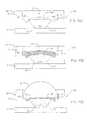
- FIGS. 1 and 2are cross-sectional side views illustrating a conventional light emitting device package
- FIGS. 3A to 3Care cross-sectional side views illustrating methods of packaging a light emitting device according to some embodiments of the present invention.
- FIG. 4Ais a top view illustrating a light emitting device package suitable for use with some embodiments of the present invention.
- FIG. 4Bis a cross-sectional side view illustrating the light emitting device package of FIG. 4A ;
- FIG. 5Ais a top view illustrating a light emitting device package according to some embodiments of the present invention.
- FIG. 5Bis a cross-sectional side view illustrating the light emitting device package of FIG. 5A ;
- FIG. 6is a cross-sectional side view illustrating a light emitting device package according to further embodiments of the present invention.
- FIG. 7is a cross-sectional side view illustrating a light emitting device package according to other embodiments of the present invention.
- FIGS. 8A to 8Care cross-sectional side views illustrating methods of packaging a light emitting device according to further embodiments of the present invention.
- FIGS. 9A to 9Care cross-sectional side views illustrating methods of packaging a light emitting device according to other embodiments of the present invention.
- FIGS. 10A to 10Care cross-sectional side views illustrating methods of packaging a light emitting device according to yet further embodiments of the present invention.
- FIG. 11is a flowchart illustrating operations for packaging a light emitting device according to some embodiments of the present invention.
- FIG. 12is a flowchart illustrating operations for packaging a light emitting device according to some other embodiments of the present invention.
- FIG. 13is a flowchart illustrating operations for packaging a light emitting device according to yet further embodiments of the present invention.
- FIG. 14is a schematic diagram illustrating path length for light traveling through a layer
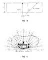
- FIG. 15is a polar plot of color-temperature for a light emitting diode (LED) emission pattern
- FIGS. 16A to 16Care cross-sectional side views illustrating methods of packaging a light emitting device including a luminescent conversion element according to further embodiments of the present invention.
- FIGS. 17A to 17Care cross-sectional side views illustrating methods of packaging a light emitting device including a luminescent conversion element according to other embodiments of the present invention.
- FIGS. 18A to 18Care cross-sectional side views illustrating methods of packaging a light emitting device including a luminescent conversion element according to some other embodiments of the present invention.
- FIG. 19is a flowchart illustrating operations for packaging a light emitting device according to some further embodiments of the present invention.
- FIG. 20Ais a polar plot of color-temperature for a light emitting diode (LED) emission pattern for a glob-top semiconductor light emitting device without a luminescence conversion element of the present invention
- FIG. 20Bis a polar plot of color-temperature for a light emitting diode (LED) emission pattern for a semiconductor light emitting device with a luminescence conversion element according to some embodiments of the present invention
- FIGS. 21A and 21Bare digitally analyzed plots of the near field emission pattern of packaged semiconductor light emitting device without a luminescence conversion element.
- FIGS. 22A and 22Bare digitally analyzed plots of the near field emission pattern of packaged semiconductor light emitting device including a luminescence conversion element according to some embodiments of the present invention.
- first, second, etc.may be used herein to describe various elements, components, regions, layers and/or sections, these elements, components, regions, layers and/or sections should not be limited by these terms. These terms are only used to distinguish one element, component, region, layer or section from another region, layer or section. Thus, a first element, component, region, layer or section discussed below could be termed a second element, component, region, layer or section without departing from the teachings of the present invention.
- semiconductor light emitting device 103may include a light emitting diode, laser diode and/or other semiconductor device which includes one or more semiconductor layers, which may include silicon, silicon carbide, gallium nitride and/or other semiconductor materials, a substrate which may include sapphire, silicon, silicon carbide and/or other microelectronic substrates, and one or more contact layers which may include metal and/or other conductive layers.
- semiconductor layerswhich may include silicon, silicon carbide, gallium nitride and/or other semiconductor materials
- a substratewhich may include sapphire, silicon, silicon carbide and/or other microelectronic substrates
- contact layerswhich may include metal and/or other conductive layers.
- ultraviolet, blue and/or green light emitting diodes (“LEDs”)may be provided. Red and/or amber LEDs may also be provided.
- LEDsultraviolet, blue and/or green light emitting diodes
- Red and/or amber LEDsmay also be provided.
- the semiconductor light emitting device 103may be gallium nitride-based LEDs or lasers fabricated on a silicon carbide substrate such as those devices manufactured and sold by Cree, Inc. of Durham, N.C.
- the present inventionmay be suitable for use with LEDs and/or lasers as described in U.S. Pat. Nos.
- the LEDs and/or lasersmay be configured to operate such that light emission occurs through the substrate.
- the substratemay be patterned so as to enhance light output of the devices as is described, for example, in the above-cited U.S. Patent Publication No. US 2002/0123164 A1.
- FIGS. 3A through 3Csome embodiments of a double-cure encapsulation process for use in packaging a light emitting device 103 are illustrated in FIGS. 3A through 3C .
- Such a double cure encapsulation processmay reduce problems associated with shrinkage of encapsulant material during curing.
- the double cure processmay include three dispense operations and two cure operations. However, it will be understood that more or less dispense operations and cure operations may also be used in packaging the light emitting device in other embodiments of the present invention.
- embodiments of the present inventionalso include a multi-dispense operation, leading to a first cure operation followed by another set of dispense and cure operations to attach a lens.
- a first predetermined amount (quantity) of an encapsulant materialis dispensed within the cavity 115 .
- the encapsulant material 112 , 114may be, for example, a liquid silicon gel, an epoxy or the like.
- the first portion 112may be dispensed to wet exposed surface portions of the light emitting device 103 , more particularly, the led chip/submount assembly 101 of the light emitting device 103 , and the substrate 102 . Portions of the reflector cup 104 may also be wet by the initial dispense.
- the quantity of encapsulant material dispensed as the first portion 112is sufficient to wet the light emitting device 103 without filling the reflective cavity to a level exceeding the height of the light emitting device 103 . In some other embodiments of the present invention, the quantity of encapsulant material dispensed as the first portion 112 is sufficient to substantially cover the light emitting device 103 without forming any air pockets in the encapsulant material 112 .
- the light emitting deviceis positioned at about a midpoint 115 m of the reflective cavity 115 .
- the encapsulant materialmay be dispensed from a dispenser 200 at a point 115 d displaced from the midpoint 115 m towards a sidewall 105 of the reflective cavity 115 so that the encapsulant material 112 is not dispensed directly onto the light emitting device 103 .
- Dispensing encapsulant material 112 directly on the light emitting device 103may cause trapping of bubbles as the encapsulant material 112 passes over the structure of the light emitting device 103 from above.
- the encapsulant material 112is dispensed on top of the light emitting device 103 die in addition to or instead of an offset dispense.
- Dispensing the encapsulant material 112may include forming a bead of the encapsulant material 112 on an end of a dispenser 200 and contacting the formed bead with the reflective cavity 115 and/or the light emitting device 103 to dispense the bead from the dispenser.
- the viscosity and/or other properties of the material used for a dispensemay be selected such that, for example, wetting occurs without bubble formation.
- coatingsmay be applied to surfaces contacted by the dispensed material to speed/retard the wetting rate. For example, using certain known cleaning procedures that leave microscopic residue, such as an oil film, selected surfaces may be treated and, thus, used to engineer the dynamics of the wetting action.
- the encapsulant material 112is expected to move or “wick” more rapidly around the inner surface of the reflector cup 104 and the sidewalls of the light emitting device 103 faster than over the top of the light emitting device 103 .
- the quantity of the first portion of dispensed encapsulant material 112may be selected to reduce or prevent the risk of forming such bubbles.
- substantially covering the light emitting device 103refers to covering enough of the structure of the light emitting device 103 so that such a bubble will not result when the remaining portion 114 of the first quantity of encapsulant material 112 , 114 is dispensed.
- the second portion 114 of the first predetermined quantity of encapsulant materialis dispensed into the reflective cavity 115 .
- the second portion 114 of the encapsulant materialin some particular embodiments of the present invention, is about twice the first portion 112 .
- the first quantity of the encapsulant material 112 , 114is cured, for example, by a heat treatment, to solidify the encapsulant material 112 , 114 .
- the level of the encapsulant material 112 , 114 within the reflective cavity 115may drop from the level 114 A to the level 114 B as a result of shrinkage of the encapsulant material 112 , 114 .
- the first portion 112is cured before the second portion 114 is dispensed into the reflective cavity 115 .
- a light converting materialsuch as a phosphor, nano-crystals, or the like
- a phosphoras a light converting material.
- other light converting materialsmay be used in place of phosphor.
- phosphormay be most beneficially utilized when positioned adjacent the emitter 103 b , in other words, directly on top of the light emitting device 103 .
- phosphormay settle from the second portion 114 into the first portion 112 , reducing the effectiveness of the phosphor addition in the second portion 114 .
- phosphorcan be added to the first portion 112 to limit such settling and/or the first portion 112 can be cured before dispensing the second portion 114 .
- multiple dispensesmay also allow the addition of a phosphor preform/wafer of a desired configuration for light conversion.
- multiple dispensesmay allow for the use of materials having different indexes of refraction to provide, for example, a buried lens (i.e., formed by the interface between two dispenses of materials with different refractive indexes).
- a second quantity of encapsulant material 116is dispensed in a predetermined amount onto the cured first quantity of encapsulant material 112 , 114 in the reflective cavity 115 .
- the second quantity 116is about equal to the first portion 112 of the first quantity of encapsulant material 112 , 114 .
- the second quantity 116may be substantially free of phosphor, however, in other embodiments of the present invention, phosphor may also be included in the second quantity 116 .
- a lens 120is positioned within the reflective cavity 115 and against the second quantity of encapsulant material 116 .
- the second quantity of encapsulant material 116is then cured, for example, by heating, to harden the encapsulant material 116 and to attach the lens 120 in the reflective cavity 115 .
- use of a double cure process as described above to encapsulate the light emitting device 103 in the package 100may reduce delamination of the cured encapsulant material 112 , 114 , 116 from the light emitting device 103 , the lens 120 and/or the reflector cup 104 .
- FIGS. 4A-4BThe reflector cup 104 shown in FIGS. 3A-3B is further illustrated in FIGS. 4A-4B .
- FIG. 4Ais a top plan view of the reflector cup 104 showing the top surfaces of the upper sidewall 105 , the lower sidewall 106 and a substantially horizontal shoulder sidewall portion 108 between the upper sidewall 105 and the lower sidewall 106 .
- FIG. 4Bis a cross-sectional view of the reflector cup 104 taken along line B-B of FIG. 4A .
- FIGS. 5A-5B , 6 and 7illustrate various alternative reflector configurations as will now be described.
- FIG. 5Ais a top plan view of a reflector cup 4 and
- FIG. 5Bis a cross-sectional view of the reflector cup 4 taken along line B-B of FIG. 5A .
- FIG. 6is a cross-sectional view of a reflector cup 4 A and FIG.
- FIG. 7is a cross-sectional view of a reflector cup 4 B.
- Each of the illustrated reflector cups 4 , 4 A, 4 Bincludes an upper sidewall 5 , an angled lower sidewall 6 and a horizontal shoulder portion 8 between the upper sidewall 5 and the lower sidewall 6 , together defining a reflective cavity 15 .
- “horizontal”refers to the general direction in which the shoulder portion 8 extends between the lower sidewall portion 6 and the upper sidewall portion 8 (i.e., as compared to the lower 6 and upper 5 sidewall portions), not to the particular angle of the shoulder portion 8 at any intermediate portion thereof (see, e.g., FIG.
- each of the reflector cups 4 , 4 A, 4 Bmay include at least one moat 18 surrounding the lower sidewall 6 , with the moat 18 being separated from the lower sidewall 6 by a lip (i.e., a projecting edge) 22 .
- the moat 18is illustrated as formed in the shoulder portion 8 .
- the moat 18could be formed by stamping, in which case the lip 22 between the moat 18 and the lower sidewall 6 may be provided with a sharp edge instead of a flat surface.
- the flat surface of the lip 22 schematically illustrated in FIG. 5Bmay actually have a more rounded profile. Too much of a rounded profile may be undesirable as will be further described with reference to FIGS. 8A-8C .
- a first moat 18is formed between the upper sidewall 5 and the lower sidewall 6 , with a first or inner lip 22 separating the lower sidewall 6 and the first moat 18 .
- a second moat 24is formed between the upper sidewall 5 and the first moat 18 .
- a second or outer lip 26separates the second moat 24 from the first moat 18 .
- a first moat 18is formed between the upper sidewall 5 and the lower sidewall 6 , with a first or inner lip 22 separating the lower sidewall 6 and the first moat 18 .
- a second moat 24is formed between the upper sidewall 5 and the first moat 18 .
- a second or outer lip 26 ′separates the second moat 24 from the first moat 18 .
- the second lip 26 ′is elevated with respect to the first lip 22 .
- the first lip 22has a peak having a radius of curvature of less than about 50 micrometers ( ⁇ m) and the second lip 26 , 26 ′ has a peak having a radius of curvature of less than about 50 ⁇ m.
- the first moat 18 and the second moat 24may be stamped features of the horizontal shoulder portion 8 .
- the second moat 24may have a width extending from the second lip 26 , 26 ′ to the upper sidewall portion 5 .
- the sloped lower sidewall portion 6may be substantially conical and may have a minimum diameter of from about 1.9 millimeters (mm) for a 500 ⁇ m light emitting device chip to about 3.2 mm for a 900 ⁇ m light emitting device chip and a maximum diameter of from about 2.6 mm for a 500 ⁇ m light emitting device chip to about 4.5 mm for a 900 ⁇ m light emitting device chip and a height of from about 0.8 mm to about 1.0 mm.
- the upper sidewall portionmay be substantially oval and have an inner diameter of from about 3.4 mm to about 5.2 mm and a height of from about 0.6 mm to about 0.7 mm.
- the horizontal shoulder portionmay have a width from the lower sidewall portion to the upper sidewall portion of from about 0.4 mm to about 0.7 mm. It will be understood that, as used herein, the terms “oval” and “conical” are intended to encompass circular, cylindrical and other shapes, including irregular shapes based on the fabrication technology used to form the reflector cup 4 , 4 A, 4 B that may, nonetheless, in combination with a substrate 2 or otherwise, operate to provide a reflector for the light emitting device 103 and retain and harden an encapsulant material 12 , 14 , 16 therein.
- the first moat 18has a width from about 0.3 mm to about 0.4 mm and the second moat 24 has a width of from about 0.3 mm to about 0.4 mm.
- the edge of the first moat 18may be a first lip 22 having a height relative to a bottom end (i.e., a top surface of the substrate 2 ) of the lower sidewall portion 6 of from about 0.79 mm to about 0.85 and the edge of the second moat 24 may be a second lip 26 having a height relative to bottom end of the lower sidewall portion 6 of from about 0.79 mm to about 0.85 mm.
- FIG. 6the edge of the first moat 18 may be a first lip 22 having a height relative to a bottom end (i.e., a top surface of the substrate 2 ) of the lower sidewall portion 6 of from about 0.79 mm to about 0.85 and the edge of the second moat 24 may be a second lip 26 having a height relative to bottom end of the lower sidewall portion 6 of from about 0.79 mm to
- the first lip 22has a height relative to a bottom end of the lower sidewall portion of from about 0.79 mm to about 0.85 mm and the second lip 26 ′ has a height relative to a bottom end of the lower sidewall portion of from about 0.9 mm to about 1.0 mm.
- the reflector cups 4 , 4 A, 4 Bmay, provide for meniscus control when packaging the light emitting device 103 in a reflector cup 4 , 4 A, 4 B.
- a distinct convex meniscusmay also be provided for different dispenses of encapsulant material and, as a result, the incidence of doming failure may be reduced.
- the provided meniscus controlmay reduce the difficulty of lens placement at a desired depth and/or angle, reduce lens wicking or squeeze-out of encapsulant material onto the top of the lens and/or allow for configuration of the optical characteristics of the packaged light emitting device.
- phosphormay be concentrated in the center (midpoint) of the package by doming (convex meniscus) of phosphor loaded encapsulant material over the midpoint of the package.
- Different optical patternsmay be provided by using multiple meniscus control techniques in combination with dispensing and/or curing variations in the process. For example, a high peaked dome of a phosphor loaded material may provide greater color spectrum uniformity of white temperature light emission with less shift to yellow towards the edges of the reflector cup by providing a more uniform length of the light path through the phosphor loaded material from the light emitting device. Similarly, where desired, a greater color spectrum variation from white at the midpoint to yellow at the edges may be provided by a flatter dome.
- meniscus controlmay allow for packaging a light emitting device without a lens by using the encapsulant material as the lens, with the meniscus being configured to provide the desired lens shape.
- FIGS. 8A-8Cillustrate methods of packaging a light emitting device, using the structural characteristics of a reflector cup for meniscus control, according to some embodiments of the present invention.
- the operations illustrated in FIGS. 8A-8Cutilize the reflector cup 4 illustrated in FIGS. 5A-5B and the double curing operations also previously described.
- a first quantity 14 of encapsulant materialis deposited in the reflective cavity 15 of the package 10 A.
- the first quantity 14may be dispensed using a separate (wetting) dispense and second dispense.
- the lip 22may be used to prevent the dispensed encapsulant material 14 from contacting and wicking up the upper sidewall 5 and forming a concave meniscus as shown in FIG. 1 .
- the dispensed encapsulant material 14is cured, for example, by heating, and may shrink down to a height indicated at 14 B. As shown in FIG. 8B , a second quantity 16 of encapsulant material is then dispensed into the cavity 15 on the cured first quantity 14 of encapsulant material.
- the second quantity 16 of encapsulant materialmay also cling to the same edge of the lip 22 to form a convex meniscus.
- the lip 22may have an inner and outer edge thereon and the second quantity 16 of encapsulant material may cling to the outer edge and the first quantity 14 may cling to the inner edge.
- the second quantity 16 of encapsulant materialmay also not contact or wick up the upper sidewall 5 to form a concave meniscus.
- the lens 20is inserted into reflective cavity 15 and brought into contact with the uncured liquid encapsulant material 16 .
- the encapsulant material 16may be squeezed out from underneath the lens 20 .
- the excess of the encapsulant material 16is squeezed into and received by the moat 18 , thus limiting wicking of the encapsulant material 16 up the sidewall 5 even after the lens 20 is inserted and the convex meniscus shown in FIG. 8B is displaced.
- the encapsulant material 16is then cured to attach the lens 20 in the package 10 A and to solidify the encapsulant material 16 .
- FIGS. 9A-9Cillustrate methods of packaging a light emitting device, using the structural characteristics of a reflector cup for meniscus control, according to some embodiments of the present invention.
- the operations illustrated in FIGS. 9A-9Cutilize the reflector cup 4 A illustrated in FIG. 6 and the double curing operations also previously described.
- a first quantity 14 of encapsulant materialis deposited in the reflective cavity 15 of the package 10 B.
- the first quantity 14may be dispensed using a distinct first (wetting) dispense and a second dispense after wetting of the light emitting device.
- the inner lip 22may be used to prevent the dispensed encapsulant material 14 from contacting and wicking up the upper sidewall 5 and forming a concave meniscus as shown in FIG. 1 .
- the dispensed encapsulant material 14is cured, for example, by heating, and may shrink down to a height indicated at 14 B. As shown in FIG. 9B , a second quantity 16 of encapsulant material is then dispensed into the reflective cavity 15 on the cured first quantity 14 of encapsulant material. In some embodiments, as illustrated in FIG. 9B , the second quantity 16 of encapsulant material clings to the outer lip 26 , forming a convex meniscus. Thus, the outer lip 26 may be used to prevent the dispensed second quantity 16 of encapsulant material from contacting and wicking up the upper sidewall 5 and forming a concave meniscus as shown in FIG. 1 .
- the lens 20is inserted into reflective cavity 15 and brought into contact with the uncured liquid encapsulant material 16 .
- the encapsulant material 16may be squeezed out from underneath the lens 20 .
- the excess of the encapsulant material 16is squeezed into and received by the second moat 24 , thus limiting wicking of the encapsulant material 16 up the sidewall 5 even after the lens 20 is inserted and the convex meniscus shown in FIG. 9B is displaced.
- the encapsulant material 16is then cured to attach the lens 20 in the package 10 B and to solidify the encapsulant material 16 .
- FIG. 9Cfurther illustrates that, in some embodiments of the present invention, the cured encapsulant 14 may be used as a stop to provide for level (depth of placement) control for the lens 20 . Such control over the positioning of the lens 20 may facilitate the production of parts with more consistent optical performance.
- the lens 20 in some embodiments of the presentis positioned without advancing into the cavity until it contacts the cured first quantity of encapsulant material 14 as a film of the encapsulant material 16 remains therebetween.
- the deviceis configured so that the lens 20 may be advanced to a position established by the first quantity of encapsulant material 14 , which position may be established with or without contact of the lens 20 to the cured encapsulant material 14 in various embodiments of the present invention.
- FIGS. 10A-10Cillustrate methods of packaging a light emitting device, using the structural characteristics of a reflector cup for meniscus control, according to some embodiments of the present invention.
- the operations illustrated in FIGS. 10A-10Cutilize the reflector cup 4 B illustrated in FIG. 7 and the double curing operations also previously described.
- a first quantity 14 of encapsulant materialis deposited in the reflective cavity 15 of the package 10 C.
- the first quantity 14may be dispensed using a separate (wetting) dispense and a second dispense.
- the inner lip 22may be used to prevent the dispensed encapsulant material 14 from contacting and wicking up the upper sidewall 5 and forming a concave meniscus as shown in FIG. 1 .
- the dispensed encapsulant material 14is cured, for example, by heating, and may shrink down to a height indicated at 14 B. As shown in FIG. 10B , a second quantity 16 of encapsulant material is then dispensed into the reflective cavity 15 on the cured first quantity 14 of encapsulant material. In some embodiments, as illustrated in FIG. 10B , the second quantity 16 of encapsulant material clings to the outer lip 26 ′, forming a convex meniscus. Thus, the outer lip 26 ′ may be used to prevent the dispensed second quantity 16 of encapsulant material from contacting and wicking up the upper sidewall 5 and forming a concave meniscus as shown in FIG. 1 .
- the lens 20is inserted into reflective cavity 15 and brought into contact with the uncured liquid encapsulant material 16 .
- the encapsulant material 16may be squeezed out from underneath the lens 20 .
- the excess of the encapsulant material 16is squeezed into and received by the second moat 24 , thus limiting wicking of the encapsulant material 16 up the sidewall 5 even after the lens 20 is inserted and the convex meniscus shown in FIG. 10B is displaced.
- the encapsulant material 16is then cured to attach the lens 20 in the package 10 C and to solidify the encapsulant material 16 .
- FIG. 10Cfurther illustrates that, in some embodiments of the present invention, the outer lip 26 ′ may be used as a stop to provide for level (depth of placement) control for the lens 20 .
- level (depth of placement) controlfor the lens 20 .
- the lens placementdoes not depend on the amount of shrinkage of the encapsulant during the first cure step.
- the placement of the lens 20need not be dependent on the amount of shrinkage of the first quantity 14 of encapsulant material as the placement depth is, instead, defined by the height of the outer lip 26 ′.
- the placementmay be more exact, which may result in improved optical performance of the package 10 C.
- FIG. 11operations may begin at Block 1100 by mounting the light emitting device on a bottom surface of a reflective cavity.
- the mounted light emitting devicehas an associated height relative to the bottom surface of the reflective cavity.
- a first quantity of encapsulant materialis dispensed into the reflective cavity including the light emitting device (Block 1120 ).
- the first quantitymay be sufficient to substantially cover the light emitting device without forming any air pockets in the encapsulant material. In some embodiments of the present invention, the first quantity may be sufficient to wet the light emitting device without filling the reflective cavity to a level exceeding the height of the light emitting device. In other embodiments of the present invention, the time/speed of dispense of the encapsulant material may be changed to reduce the formation of air pockets in the encapsulant material. In yet further embodiments, a single dispense may be used, for example, with a slow dispense rate, from a small dispense needle, low pressure, or the like, allowing an air pocket to potentially form and then cave/collapse before enough encapsulant material has been dispensed to prevent collapse of the air pocket.
- the first (wetting) dispense and second dispensemay be provided by a continuous dispense at a selected rate of a selected viscosity encapsulant material that allows cave/collapse of a formed air pocket during the dispense operation
- the first quantitymay be sufficient to wet the light emitting device without filling the reflective cavity to a level exceeding the height of the light emitting device.
- a second quantity of encapsulant materialis dispensed onto the first quantity of encapsulant material (Block 1130 ).
- the dispensed first and second quantity of encapsulant materialare then cured (Block 1140 ).
- the first dispensed wetting quantity of encapsulant materialmay be cured before the remainder of the encapsulant material is dispensed.
- the first quantity 12 , 14 and the second quantity 16 of the encapsulant materialmay be the same or different materials.
- the first 12 and second 14 portions of the first quantity of the encapsulant materialmay be the same or different materials. Examples of materials that may be used as an encapsulant material in various embodiments of the present invention include silicon.
- Operations related to packaging a semiconductor light emitting device according to some embodiments of the present invention using meniscus controlwill now be described with reference to the flowchart illustration of FIG. 12 .
- operationsmay begin at Block 1200 with mounting of the light emitting device 103 in a reflective cavity 15 of a reflector 5 .
- Encapsulant materialis dispensed into the reflective cavity 15 including the light emitting device 103 therein to cover the light emitting device 103 and to form a convex meniscus of encapsulant material in the reflective cavity extending from an edge of the moat without contacting the upper sidewall 5 of the reflector 4 , 4 A, 4 B (Block 1210 ).
- operations at Block 1210provide for formation of a convex meniscus extending from an outer edge of the meniscus that is at a height positioning the outer edge of the meniscus within the reflective cavity 15 .
- selection of materials used for the upper sidewall 5 and the encapsulant material 12 , 14 , 16may facilitate formation of a convex, rather than concave, meniscus extending into the reflective cavity 15 .
- the encapsulant material 12 , 14 , 16is in the reflective cavity 15 (Block 1220 ).
- insertion of the lens 20may include collapsing the convex meniscus and moving a portion of the encapsulant material 12 , 14 , 16 into the moat 18 , 24 with the lens 20 and then curing the encapsulant material 12 , 14 , 16 to attach the lens 20 in the reflective cavity 15 .
- the encapsulant material 12 , 14 , 16may be cured to form a lens for the packaged light emitting device 103 from the encapsulant material 12 , 14 , 16 and the encapsulant material 12 , 14 , 16 may be dispensed to form a convex meniscus providing a desired shape of the lens.
- Embodiments of methods of packaging a semiconductor light emitting device 103 in a reflector 4 , 4 A, 4 B having a moat 18 , 24 positioned between a lower 6 and an upper 5 sidewall thereof, the upper 5 and lower 6 sidewall defining a reflective cavity 15 , using a multiple dispense and/or cure operationwill now be further described with reference to FIG. 13 .
- operationsbegin at Block 1300 by dispensing a first quantity 14 of encapsulant material into the reflective cavity 15 to form a first convex meniscus.
- the first quantity 14 of encapsulant materialis cured (Block 1310 ).
- a second quantity 16 of encapsulant materialis dispensed onto the cured first quantity 14 of encapsulant material to form a second convex meniscus of encapsulant material in the reflective cavity 15 extending from an edge of the moat 18 , 24 without contacting the upper sidewall 5 of the reflector 4 , 4 A, 4 B (Block 1320 ).
- the second convex meniscus and the first convex meniscus of encapsulant materialmay both extend from the same edge of the moat 18 as illustrated in FIG. 8B .
- the moat 18 , 24may have an inner edge and an outer edge, such as the first lip 22 and the second lip 26 , 26 ′, and the second convex meniscus of encapsulant material extends from the outer edge (second lip 26 , 26 ′) of the moat 18 , 24 and the first convex meniscus of encapsulant material extends from the inner edge (first lip 22 ) of the moat 18 , 24 .
- the inner moat 18may be configured to limit wicking of encapsulant material 14 outwardly along the horizontal shoulder portion 8 to allow formation of a first convex meniscus of encapsulant material dispensed into the reflective cavity 15 .
- the outer moat 24may be configured to limit wicking of encapsulant material outwardly along the horizontal shoulder portion 8 to allow formation of a second convex meniscus of encapsulant material dispensed into the reflective cavity 15 .
- the lens 20is positioned in the reflective cavity 15 proximate the dispensed second quantity 16 of encapsulant material (Block 1330 ). Positioning the lens 20 may include collapsing the second convex meniscus and moving a portion of the second quantity 16 of encapsulant material into the outer moat 24 with the lens 20 as illustrated in FIGS. 9C and 10C .
- the second lip 26 ′may have a height greater than that of the first lip 22 . The height of the second lip 26 ′ may be selected to provide a desired position for the lens 20 and the lens 20 may be moved into the reflective cavity 15 until it contacts the second lip 26 ′.
- the lens 20is advanced into the reflective cavity 15 until it contacts the cured first quantity 14 of encapsulant material and the dispensed first quantity 14 of encapsulant material sufficient to establish a desired position for the lens 20 in the reflective cavity 15 .
- the dispensed second quantity 16 of encapsulant materialis cured to attach the lens 20 in the reflective cavity 15 (Block 1340 ).
- FIGS. 11-13 and the schematic illustrations of FIGS. 8A-8C , 9 A- 9 C and 10 A- 10 Cillustrate the functionality and operation of possible implementations of methods for packaging a light emitting device according to some embodiments of the present invention. It should be noted that, in some alternative implementations, the acts noted in describing the figures may occur out of the order noted in the figures. For example, two blocks/operations shown in succession may, in fact, be executed substantially concurrently, or may be executed in the reverse order, depending upon the functionality involved.
- different optical patternsmay be provided by using multiple meniscus control techniques in combination with dispensing and/or curing variations in the process.
- a high peaked dome of a phosphor loaded materialmay provide greater color spectrum uniformity of white temperature light emission with less shift to yellow towards the edges of the reflector cup by providing a more uniform length of the light path through the phosphor loaded material from the light emitting device.
- Embodiments of the present inventionprovide one or more light emitting devices (i.e. chips) mounted in an optical cavity with a phosphor-loaded luminescent conversion layer formed in proximity to the light emitting device (i.e. adjacent or in a spaced relationship thereto).
- a phosphor-loaded luminescent conversion layerformed in proximity to the light emitting device (i.e. adjacent or in a spaced relationship thereto).
- the luminescent conversion layershould have a thickness variation less than or equal to ten percent (10%) of the average thickness of the luminescent conversion layer.
- ten percent (10%)ten percent
- such a requirementmeans that light emission from the optical cavity may travel substantially different path lengths through the luminescent conversion layer depending on the angle of emission, resulting in non-uniform wavelength conversion (and therefore non-uniform correlated color temperature or CCT) as a function of viewing angle.
- FIG. 15is a polar plot of an emission pattern showing substantial sidelobes at off-axis angles of emission that may result from a conventional glob-top type semiconductor light emitting device including a light emitting diode (LED).
- LEDlight emitting diode
- the methods disclosed herein for meniscus controlmay be employed to form a shaped luminescent conversion region or element that may result in improved color uniformity.
- Improved color uniformitymay be quantified, for example, by improved angular uniformity of correlated color temperature or reduced variation in CCT across all viewing angles. Alternatively, the improved uniformity is evidenced by near field optical measurements as a reduced spatial CCT variation across the emission surface of the LED.
- a phosphor-loaded luminescent conversion region or elementis characterized by a non-uniform thickness that is greater in the middle of the optical cavity and smaller near the sidewalls of the optical cavity.
- a phosphor-loaded luminescent conversion region or elementis thickest at the center of the optical cavity and becomes thinner as it extends radially outward toward the edge of the luminescent conversion region.
- the thickness variation of the phosphor-loaded luminescent conversion regionis greater than 10% of the maximum thickness of the luminescent conversion region.
- the luminescent conversion region or elementis shaped in the form of a biconvex, plano-convex or concavo-convex region.
- the luminescent conversion elementcomprises a pre-formed structure, such as a molded plastic phosphor-loaded piece part, that is inserted into the reflective cavity of the package.
- FIGS. 16A-16Cillustrate methods of packaging a light emitting device and resulting devices using the structural characteristics of a reflector cup for meniscus control.
- the operations illustrated in FIGS. 16A-16Cutilize the reflector cup 4 illustrated in FIGS. 5A-5B and multiple curing operations similar to those previously described.
- a first quantity 14 of encapsulant materialis deposited in the reflective cavity 15 of the package 10 .
- the first quantity 14may be dispensed using a separate (wetting) pre-dispense followed by another dispense.
- encapsulant material 14With proper control of the amount of encapsulant material dispensed, surface tension will cause the liquid encapsulant material 14 to cling to the lip 22 , forming a meniscus as illustrated in FIG. 16A at a height indicated at 14 A.
- the initial meniscus formed by encapsulant material 14may be concave, convex or substantially flat as illustrated in FIG. 16A .
- the dispensed encapsulant material 14is cured, for example, by heating, and may shrink down to a lower height indicated at 14 B.
- the cured encapsulant material 14shrinks down to form a concave surface 14 C, which in three dimensions may be substantially bowl-shaped (i.e. lowest in the center and sloping radially upwards).
- the encapsulant material 14may be pre-cured, i.e. exposed to a lower temperature or for shorter cure times, such that the encapsulant material does not completely solidify but rather merely forms a solid “skin” over its surface.
- the purpose of forming the skinis to prevent subsequently dispensed encapsulant material from intermixing with the first encapsulant material 14 .
- Subsequent encapsulant dispensesmay contain wavelength conversion materials (such as phosphors) and, as discussed above, it may be desirable for the phosphor-loaded luminescent conversion region to retain a characteristic shape rather than becoming intermixed with the first encapsulant material 14 .
- Subjecting the first encapsulant layer 14 to a pre-cure instead of a full curemay speed the manufacturing process and may result in an improved interface between the first encapsulant material and subsequent encapsulant regions.
- a second quantity 16 of encapsulant materialis then dispensed into the cavity 15 onto bowl-shaped surface 14 C.
- the second encapsulant material 16includes a luminescent wavelength conversion material, such as a phosphor, in the illustrated embodiments.
- the first encapsulant material 14includes no luminescent wavelength conversion material.
- the first encapsulant material 14includes a lower concentration of luminescent wavelength conversion material than the second encapsulant material 16 .
- the second encapsulant material 16may also cling to the same edge of the lip 22 to form a convex meniscus.
- the second encapsulant material 16is then cured (along with the first encapsulant material 14 if the first encapsulant material 14 was only pre-cured before the second encapsulant material 16 was dispensed).
- the second encapsulant material 16may also be pre-cured, i.e. exposed to a lower temperature or for shorter cure times, in order to prevent or reduce the risk of subsequently dispensed encapsulant material from intermixing with the second encapsulant material 16 .
- the second encapsulant material 16may be more fully cured in order to solidify the material before the lens 20 is inserted into the cavity 15 . As discussed below, once solidified, the second encapsulant material 16 may act as a mechanical stop to assist with correct placement of the lens 20 .
- the resulting cured (or pre-cured) second encapsulant material 16defines a luminescent conversion element 19 characterized by a non-uniform thickness that is greatest near the center of the optical cavity and that decreases radially towards the outer edge of the luminescent conversion element 19 .
- the luminescent conversion element 19is a bi-convex structure including a convex upper surface 19 A and a convex lower surface 19 B.
- the luminescent conversion element 19may be a pre-formed phosphor-loaded insert that is placed within the reflective cavity 15 of the package 10 .
- Such a structuremay have some advantages for device performance and manufacturability.
- forming the luminescent conversion element 19 as a pre-formed insertmay result in improved quality control as the pre-formed inserts may be individually tested before insertion.
- liquid phosphor-loaded materialdoes not have to be used in the final assembly process. This can provide benefits, as phosphor-loaded material can be abrasive and can interfere with the operation of automated machinery.
- a cure stepmay be avoided by forming the phosphor-loaded luminescent conversion element 19 as a pre-formed insert.
- a transparent, convex hemispherical mold(not shown) may be placed over first encapsulant 14 before or after it is cured in order to receive the second encapsulant 16 .
- the second encapsulant 16Upon curing, the second encapsulant 16 will take the shape of the convex hemispherical mold, which may provide improved control over the final shape of the luminescent conversion element 19 .
- a quantity of a third encapsulant material 17is dispensed within the cavity 15 as further illustrated in FIG. 16B .
- the third encapsulant material 17may be an optically transparent material, such as silicone or epoxy, with no luminescent conversion material or a low concentration of luminescent conversion material. Because the third encapsulant material 17 is dispensed following a cure or pre-cure step, the phosphor conversion material embedded in luminescent conversion element 19 may not substantially intermix with the third encapsulant material 17 .
- the lip 22may have an inner and outer edge thereon and the third quantity 17 of encapsulant material may cling to the outer edge of the lip 22 , forming a convex meniscus above luminescent conversion element 19 .
- the third encapsulant material 17may also not contact or wick up the upper sidewall 5 to form a concave meniscus.
- the lens 20is inserted into reflective cavity 15 and brought into contact with the uncured liquid third encapsulant material 17 .
- the third encapsulant material 17may be squeezed out from underneath the lens 20 .
- the excess of the third encapsulant material 17is squeezed into and received by the moat 18 , thus limiting wicking of the encapsulant material 17 up the sidewall 5 even after the lens 20 is inserted and the convex meniscus of third encapsulant material 17 shown in FIG. 16B is displaced.
- the encapsulant material 17is then cured to attach the lens 20 in the package 10 and to solidify the encapsulant material 17 .
- the lens 20is advanced into the reflective cavity 15 until it contacts the luminescent conversion element 19 to establish a desired position for the lens 20 in the reflective cavity 15 .
- the luminescent conversion element 19may act as a mechanical stop to assure correct placement of the lens 20 .
- the lens 20is advanced into the reflective cavity 15 until it contacts a lip formed in the cavity sufficient to establish a desired position for the lens 20 in the reflective cavity 15 , as illustrated in FIG. 10C .
- the first encapsulant material 14may include a scattering material embedded therein for scattering light passing therethrough, which may better improve angular uniformity of light emission.
- the first encapsulant material 14may have a high index of refraction for better light extraction from the device 103 . If luminescent conversion element 19 has a different index of refraction from that of the first encapsulant material 14 , light rays passing through the interface between the two regions may be refracted, altering the light emission patterns of the device. If the index of refraction of the luminescent conversion element 19 is lower than that of first encapsulant material 14 , light rays will tend to be refracted away from the normal direction, which may result in a more pronounced path length difference. The shape of luminescent conversion element 19 may be chosen or altered to offset such effects. For example, as discussed above, the luminescent conversion element 19 may be bi-convex, piano-convex or concavo-convex.
- FIGS. 17A-17CAn example of forming a plano-convex luminescent conversion element using meniscus control techniques described herein is illustrated in FIGS. 17A-17C .
- a quantity of first encapsulant material 14is deposited in the reflective cavity 15 of the package 10 .
- surface tensionwill cause the liquid encapsulant material 14 to cling to the lip 22 , forming a convex meniscus as illustrated in FIG. 17A at a height indicated at 14 A.
- the first encapsulant material 14relaxes to a height indicated at 14 B, forming an approximately flat surface 14 C.
- Second encapsulant material 16is then dispensed, forming a convex meniscus that clings to an inner or outer edge of lip 22 . After curing, the second encapsulant material 16 forms a plano-convex luminescent conversion element 19 having a convex surface 19 A above a planar surface 19 B. The remaining manufacturing steps are generally the same as were described above in connection with FIGS. 16A-16C .
- the luminescent conversion element 19may be formed as a plano-convex region with a planar region above a convex surface ( FIG. 18A ), a concavo-convex region with a convex surface above a concave surface ( FIG. 18B ) or a concavo-convex region with a concave surface above a convex surface ( FIG. 18C ).
- the luminescent conversion element 19includes a wavelength conversion material, such as a phosphor material.
- the first encapsulant material 14 and the third encapsulant material 17may have no wavelength conversion material or a lower concentration of wavelength conversion material compared to the luminescent conversion element 19 .
- 16A-C , 17 A-C and 18 A-Care illustrated in connection with a reflector cup 4 as illustrated in FIGS. 5A-B , the techniques described above are applicable to other reflector cup designs, including reflector cups that include multiple moats and reflector cups that do not include a moat.
- Embodiments of methods of packaging a semiconductor light emitting device 103 in a reflector 4 having a lower 6 and an upper 5 sidewall defining a reflective cavity 15 and incorporating a phosphor-loaded luminescent conversion element 19 with a non-uniform thicknesswill now be further described with reference to FIG. 19 .
- operationsbegin at Block 1900 by dispensing a first quantity 14 of encapsulant material into the reflective cavity 15 to form a first meniscus.
- the meniscusmay have a convex, concave or substantially planar shape depending on the desired final shape of the luminescent conversion element 19 .
- the shape of the meniscusis determined by the physical dimensions of the reflector 4 and the quantity of encapsulant dispensed into the cavity.
- Branch A of the flowchart of FIG. 19may be followed if it is desired to form the luminescent conversion element 19 using meniscus control methods.
- Branch Bmay be followed if it is desired to form luminescent conversion element 19 using a pre-formed insert.
- a second quantity 16 of encapsulant material containing a concentration of wavelength conversion material that is greater than that of first encapsulant material 14is dispensed onto the cured first encapsulant material 14 (Block 1920 ).
- the second encapsulant material 16is then cured or pre-cured to form a luminescent conversion element 19 (Block 1930 ).
- a pre-formed luminescent conversion element 19is inserted into the cavity 15 in contact with first encapsulant material 14 (Block 1950 ).
- the step of curing the first quantity of encapsulant materialmay be performed after insertion of the pre-formed luminescent conversion element 19 .
- third encapsulant material 17is dispensed within cavity 15 (Block 1960 ).
- the lens 20is positioned in the reflective cavity 15 proximate the dispensed third quantity 17 of encapsulant material (Block 1970 ).
- Positioning the lens 20may include collapsing a meniscus of third encapsulant material 17 and moving a portion of the third quantity 17 of encapsulant material into a moat 18 , 24 with the lens 20 as illustrated in FIGS. 9C , 10 C, 16 C and 17 C.
- FIG. 9Ca meniscus of third encapsulant material
- the packagemay include a second lip 26 ′ having a height greater than that of the first lip 22 .
- the height of the second lip 26 ′may be selected to provide a desired position for the lens 20 and the lens 20 may be moved into the reflective cavity 15 until it contacts the second lip 26 ′.
- the lens 20is advanced into the reflective cavity 15 until it contacts the luminescent conversion element 19 sufficient to establish a desired position for the lens 20 in the reflective cavity 15 .
- the dispensed third quantity 17 of encapsulant materialis cured to attach the lens 20 in the reflective cavity 15 (Block 1980 ).
- FIG. 19illustrates the functionality and operation of possible implementations of methods for packaging a light emitting device according to some embodiments of the present invention. It should be noted that, in some alternative implementations, the acts noted in describing the figures may occur out of the order noted in the figures. For example, two blocks/operations shown in succession may, in fact, be executed substantially concurrently, or may be executed in the reverse order, depending upon the functionality involved.
- FIG. 20Ais a polar plot of color-temperature for a glob-top light emitting diode (LED) emission pattern without a luminescent conversion element of the present invention generated using a goniometer.
- FIG. 20Bis a polar plot of color-temperature for a light emitting diode (LED) emission pattern with a luminescent conversion element according to some embodiments of the present invention.
- a comparison of FIG. 20B to FIG. 20Ashows an improvement in uniformity provided by the luminescent conversion region (i.e., the radius of the emission pattern is more uniform in FIG. 20B ). As seen in FIG.
- the packaged semiconductor light emitting devicehas a minimum color temperature (5.3 kK at about ⁇ 85°) approximately 26 percent below a maximum color temperature (7.2 kK at about 0°) thereof over the measured 180 (+/ ⁇ 90 from normal or central axis)-degree range of emission angles.
- Various embodiments of the present inventionmay provide a minimum color temperature no more than 30 percent below a maximum color temperature for the semiconductor light emitting device package over a measured 180 (+/ ⁇ 90 from normal or central axis)-degree range of emission angles or over a measured 120 (+/ ⁇ 45 from normal or central axis)-degree range of emission angles.
- FIGS. 21A and 21B and 22 A and 22 Bfurther illustrate improvement in color uniformity obtained according to some embodiments of the present invention.
- FIGS. 21A and 21Bare digitally analyzed plots of the near field emission pattern of a first packaged device including a substrate/reflector assembly in which a Model C460XB900 light emitting diode manufactured by Cree, Inc. was mounted.
- 0.0030 cc Silicone(example: vendor e.g. Nye Synthetic Lubricants) mixed with 4% YAG doped with Ce Phosphor (example: from Philips)_was pre-dispensed over the light emitting device, followed by a dispense of 0.0070 cc of the same encapsulant.
- the dispensed encapsulantwas cured for 60 minutes at a temperature of 70 C.
- a second quantity of 0.0050 cc of clear encapsulant materialwas then dispensed into the optical cavity and a lens was positioned in the optical cavity in contact with the second quantity of encapsulant.
- the second quantity of encapsulantwas then cured for 60 minutes at a temperature of 70 C.
- the resulting structurewas then energized and the near field emission pattern was recorded and analyzed.
- the emission patternshows a total CCT variation of approximately 2000K over the measured 180 (+/ ⁇ 90 from normal or central axis)-degree range of emission angles.
- FIGS. 22A and 22Bare digitally analyzed plots of the near field emission pattern of a second packaged device including a substrate/reflector assembly in which a C460XB900 light emitting diode manufactured by Cree, Inc. was mounted.
- 0.0020 cc of clear silicone(example: vendor e.g. Nye Synthetic Lubricants) was pre-dispensed over the light emitting device, followed by a first dispense of 0.0035 cc of the same encapsulant.
- the first encapsulant(including the pre-dispensed encapsulant) contained no wavelength conversion material.
- the first encapsulantwas cured for 60 minutes at a temperature of 70 C to form a concave meniscus.
- a second quantity of 0.0045 cc encapsulant material containing a wavelength conversion phosphor, namely 7% by weight of YAG doped with Ce Phosphor (example: from Philips)was then dispensed into concave meniscus formed by the first encapsulant.
- the second encapsulantwas then cured for 60 minutes at a temperature of 70 C to form a luminescent conversion element having a thickness that was greatest at the center of the optical cavity and that decreased radially outward.
- a third quantity of 0.0050 cc encapsulant(which did not contain any wavelength conversion material) was then dispensed into the optical cavity and a lens was positioned in the optical cavity in contact with the third quantity of encapsulant.
- the third quantity of encapsulantwas then cured for 60 minutes at a temperature of 70 C.
- the resulting structurewas then energized and the near field emission pattern was recorded and analyzed.
- the emission patternshows a total CCT variation of approximately 500K over the same range of emission angles.
- a CCT variation of less than about 1000Kis provided over a measured 180, 120 or 90 (centered on normal or central axis)-degree range of emission angles.
- a CCT variation of less than about 2000Kis provided over a measured 180, 120 or 90 (centered on normal or central axis)-degree range of emission angles.
- a CCT variation of less than about 500Kis provided over a measured 120 or 90 (centered on normal or central axis)-degree range of emission angles.
- the CCT variation referred to hereinis based on a primary emission pattern of a device including primary optics processed with the device without the use of any additional secondary optics added to or used in combination with the packaged semiconductor light emitting device to improve color variation.
- Primary opticsrefers to the optics integral to the device, such as a luminescent conversion element in combination with a lens built into the device as described for various embodiments of the present invention herein.
Landscapes
- Led Device Packages (AREA)
Abstract
Description
Claims (32)
Priority Applications (3)
| Application Number | Priority Date | Filing Date | Title |
|---|---|---|---|
| US12/398,626US7799586B2 (en) | 2004-03-31 | 2009-03-05 | Semiconductor light emitting devices including a luminescent conversion element and methods for packaging the same |
| US12/886,001US8039859B2 (en) | 2004-03-31 | 2010-09-20 | Semiconductor light emitting devices including an optically transmissive element |
| US13/272,731US20120037931A1 (en) | 2004-03-31 | 2011-10-13 | Semiconductor light emitting devices including an optically transmissive element and methods for packaging the same |
Applications Claiming Priority (4)
| Application Number | Priority Date | Filing Date | Title |
|---|---|---|---|
| US55831404P | 2004-03-31 | 2004-03-31 | |
| US63770004P | 2004-12-21 | 2004-12-21 | |
| US11/055,194US7517728B2 (en) | 2004-03-31 | 2005-02-10 | Semiconductor light emitting devices including a luminescent conversion element |
| US12/398,626US7799586B2 (en) | 2004-03-31 | 2009-03-05 | Semiconductor light emitting devices including a luminescent conversion element and methods for packaging the same |
Related Parent Applications (1)
| Application Number | Title | Priority Date | Filing Date |
|---|---|---|---|
| US11/055,194ContinuationUS7517728B2 (en) | 2004-03-31 | 2005-02-10 | Semiconductor light emitting devices including a luminescent conversion element |
Related Child Applications (1)
| Application Number | Title | Priority Date | Filing Date |
|---|---|---|---|
| US12/886,001ContinuationUS8039859B2 (en) | 2004-03-31 | 2010-09-20 | Semiconductor light emitting devices including an optically transmissive element |
Publications (2)
| Publication Number | Publication Date |
|---|---|
| US20090224277A1 US20090224277A1 (en) | 2009-09-10 |
| US7799586B2true US7799586B2 (en) | 2010-09-21 |
Family
ID=35054898
Family Applications (4)
| Application Number | Title | Priority Date | Filing Date |
|---|---|---|---|
| US11/055,194Active2025-12-16US7517728B2 (en) | 2004-03-31 | 2005-02-10 | Semiconductor light emitting devices including a luminescent conversion element |
| US12/398,626Expired - LifetimeUS7799586B2 (en) | 2004-03-31 | 2009-03-05 | Semiconductor light emitting devices including a luminescent conversion element and methods for packaging the same |
| US12/886,001Expired - LifetimeUS8039859B2 (en) | 2004-03-31 | 2010-09-20 | Semiconductor light emitting devices including an optically transmissive element |
| US13/272,731AbandonedUS20120037931A1 (en) | 2004-03-31 | 2011-10-13 | Semiconductor light emitting devices including an optically transmissive element and methods for packaging the same |
Family Applications Before (1)
| Application Number | Title | Priority Date | Filing Date |
|---|---|---|---|
| US11/055,194Active2025-12-16US7517728B2 (en) | 2004-03-31 | 2005-02-10 | Semiconductor light emitting devices including a luminescent conversion element |
Family Applications After (2)
| Application Number | Title | Priority Date | Filing Date |
|---|---|---|---|
| US12/886,001Expired - LifetimeUS8039859B2 (en) | 2004-03-31 | 2010-09-20 | Semiconductor light emitting devices including an optically transmissive element |
| US13/272,731AbandonedUS20120037931A1 (en) | 2004-03-31 | 2011-10-13 | Semiconductor light emitting devices including an optically transmissive element and methods for packaging the same |
Country Status (6)
| Country | Link |
|---|---|
| US (4) | US7517728B2 (en) |
| EP (1) | EP1730793B1 (en) |
| JP (1) | JP5285271B2 (en) |
| KR (1) | KR20060135848A (en) |
| TW (2) | TWI452740B (en) |
| WO (1) | WO2005098976A2 (en) |
Cited By (14)
| Publication number | Priority date | Publication date | Assignee | Title |
|---|---|---|---|---|
| US20090244882A1 (en)* | 2006-06-14 | 2009-10-01 | Koninklijke Philips Electronics N.V. | Lighting device |
| USD640210S1 (en)* | 2009-06-15 | 2011-06-21 | Toyoda Gosei Co., Ltd. | Light emitting diode |
| US20120026747A1 (en)* | 2010-07-30 | 2012-02-02 | Ichikoh Industries, Ltd. | Light source unit of semiconductor-type light source of vehicle lighting device and vehicle lighting device |
| US8128249B2 (en) | 2007-08-28 | 2012-03-06 | Qd Vision, Inc. | Apparatus for selectively backlighting a material |
| US20120294025A1 (en)* | 2011-05-18 | 2012-11-22 | Samsung Electronics Co., Ltd. | Light emitting device assembly and headlamp including the same |
| US8405063B2 (en) | 2007-07-23 | 2013-03-26 | Qd Vision, Inc. | Quantum dot light enhancement substrate and lighting device including same |
| US8491140B2 (en) | 2010-11-05 | 2013-07-23 | Cree, Inc. | Lighting device with multiple emitters and remote lumiphor |
| US8791642B2 (en) | 2011-03-03 | 2014-07-29 | Cree, Inc. | Semiconductor light emitting devices having selectable and/or adjustable color points and related methods |
| US8796952B2 (en) | 2011-03-03 | 2014-08-05 | Cree, Inc. | Semiconductor light emitting devices having selectable and/or adjustable color points and related methods |
| US8876272B2 (en) | 2007-06-25 | 2014-11-04 | Qd Vision, Inc. | Compositions and methods including depositing nanomaterial |
| US8882298B2 (en) | 2012-12-14 | 2014-11-11 | Remphos Technologies Llc | LED module for light distribution |
| US9140429B2 (en) | 2010-10-14 | 2015-09-22 | Cree, Inc. | Optical element edge treatment for lighting device |
| US9182091B2 (en) | 2012-12-14 | 2015-11-10 | Remphos Technologies Llc | LED panel light fixture |
| US9587790B2 (en) | 2013-03-15 | 2017-03-07 | Cree, Inc. | Remote lumiphor solid state lighting devices with enhanced light extraction |
Families Citing this family (153)
| Publication number | Priority date | Publication date | Assignee | Title |
|---|---|---|---|---|
| CA2523544A1 (en) | 2003-04-30 | 2004-11-18 | Cree, Inc. | High powered light emitter packages with compact optics |
| US7005679B2 (en) | 2003-05-01 | 2006-02-28 | Cree, Inc. | Multiple component solid state white light |
| US7915085B2 (en) | 2003-09-18 | 2011-03-29 | Cree, Inc. | Molded chip fabrication method |
| US7517728B2 (en)* | 2004-03-31 | 2009-04-14 | Cree, Inc. | Semiconductor light emitting devices including a luminescent conversion element |
| US7837348B2 (en)* | 2004-05-05 | 2010-11-23 | Rensselaer Polytechnic Institute | Lighting system using multiple colored light emitting sources and diffuser element |
| US7791061B2 (en) | 2004-05-18 | 2010-09-07 | Cree, Inc. | External extraction light emitting diode based upon crystallographic faceted surfaces |
| US7456499B2 (en)* | 2004-06-04 | 2008-11-25 | Cree, Inc. | Power light emitting die package with reflecting lens and the method of making the same |
| US7534633B2 (en) | 2004-07-02 | 2009-05-19 | Cree, Inc. | LED with substrate modifications for enhanced light extraction and method of making same |
| US9929326B2 (en) | 2004-10-29 | 2018-03-27 | Ledengin, Inc. | LED package having mushroom-shaped lens with volume diffuser |
| US8134292B2 (en)* | 2004-10-29 | 2012-03-13 | Ledengin, Inc. | Light emitting device with a thermal insulating and refractive index matching material |
| US8816369B2 (en) | 2004-10-29 | 2014-08-26 | Led Engin, Inc. | LED packages with mushroom shaped lenses and methods of manufacturing LED light-emitting devices |
| US8324641B2 (en)* | 2007-06-29 | 2012-12-04 | Ledengin, Inc. | Matrix material including an embedded dispersion of beads for a light-emitting device |
| US7939842B2 (en) | 2005-01-27 | 2011-05-10 | Cree, Inc. | Light emitting device packages, light emitting diode (LED) packages and related methods |
| DE102005020908A1 (en)* | 2005-02-28 | 2006-08-31 | Osram Opto Semiconductors Gmbh | Lighting device for back lighting of liquid crystal display, has optical unit with radiation emission surface which has convex curved partial region that partially surrounds concave curved partial region in distance to optical axis |
| WO2006099741A1 (en)* | 2005-03-24 | 2006-09-28 | Tir Systems Ltd. | Solid-state lighting device package |
| WO2006105638A1 (en)* | 2005-04-05 | 2006-10-12 | Tir Systems Ltd. | Electronic device package with an integrated evaporator |
| US7365371B2 (en)* | 2005-08-04 | 2008-04-29 | Cree, Inc. | Packages for semiconductor light emitting devices utilizing dispensed encapsulants |
| CN101351891B (en) | 2005-12-22 | 2014-11-19 | 科锐公司 | lighting device |
| US7521728B2 (en)* | 2006-01-20 | 2009-04-21 | Cree, Inc. | Packages for semiconductor light emitting devices utilizing dispensed reflectors and methods of forming the same |
| EP1843400A1 (en)* | 2006-03-16 | 2007-10-10 | Centro Ricerche Plast-Optica S.r.l. | Light emission device and corresponding manufacturing process |
| KR100738933B1 (en)* | 2006-03-17 | 2007-07-12 | (주)대신엘이디 | LED module for lighting |
| DE102006014247B4 (en)* | 2006-03-28 | 2019-10-24 | Robert Bosch Gmbh | Image recording system and method for its production |
| US8469760B2 (en)* | 2006-03-31 | 2013-06-25 | Dowa Electronics Materials Co., Ltd. | Light emitting device and method for producing same |
| US8969908B2 (en) | 2006-04-04 | 2015-03-03 | Cree, Inc. | Uniform emission LED package |
| US9780268B2 (en)* | 2006-04-04 | 2017-10-03 | Cree, Inc. | Submount based surface mount device (SMD) light emitter components and methods |
| USD738832S1 (en) | 2006-04-04 | 2015-09-15 | Cree, Inc. | Light emitting diode (LED) package |
| EP3422425B1 (en)* | 2006-04-24 | 2022-02-23 | CreeLED, Inc. | Side-view surface mount white led |
| KR100764391B1 (en)* | 2006-04-25 | 2007-10-05 | 삼성전기주식회사 | Light emitting diode module |
| EP1850399A1 (en)* | 2006-04-25 | 2007-10-31 | ILED Photoelectronics Inc. | Sealing structure for a white light emitting diode |
| KR100731678B1 (en)* | 2006-05-08 | 2007-06-22 | 서울반도체 주식회사 | Chip type light emitting diode package and light emitting device having the same |
| US7655486B2 (en)* | 2006-05-17 | 2010-02-02 | 3M Innovative Properties Company | Method of making light emitting device with multilayer silicon-containing encapsulant |
| US7989823B2 (en)* | 2006-06-08 | 2011-08-02 | Hong-Yuan Technology Co., Ltd. | Light emitting system, light emitting apparatus and forming method thereof |
| US7906794B2 (en)* | 2006-07-05 | 2011-03-15 | Koninklijke Philips Electronics N.V. | Light emitting device package with frame and optically transmissive element |
| TWI321857B (en)* | 2006-07-21 | 2010-03-11 | Epistar Corp | A light emitting device |
| US7804147B2 (en)* | 2006-07-31 | 2010-09-28 | Cree, Inc. | Light emitting diode package element with internal meniscus for bubble free lens placement |
| US7943952B2 (en)* | 2006-07-31 | 2011-05-17 | Cree, Inc. | Method of uniform phosphor chip coating and LED package fabricated using method |
| JP5205724B2 (en)* | 2006-08-04 | 2013-06-05 | 日亜化学工業株式会社 | Light emitting device |
| US8425271B2 (en)* | 2006-09-01 | 2013-04-23 | Cree, Inc. | Phosphor position in light emitting diodes |
| US7910938B2 (en)* | 2006-09-01 | 2011-03-22 | Cree, Inc. | Encapsulant profile for light emitting diodes |
| US20080064131A1 (en)* | 2006-09-12 | 2008-03-13 | Mutual-Tek Industries Co., Ltd. | Light emitting apparatus and method for the same |
| KR100757826B1 (en)* | 2006-09-29 | 2007-09-11 | 서울반도체 주식회사 | Side Light Emitting Diode Package |
| BRPI0718086A2 (en)* | 2006-10-31 | 2013-11-05 | Tir Technology Lp | LIGHTING DEVICE PACKAGING |
| US10295147B2 (en) | 2006-11-09 | 2019-05-21 | Cree, Inc. | LED array and method for fabricating same |
| US7769066B2 (en) | 2006-11-15 | 2010-08-03 | Cree, Inc. | Laser diode and method for fabricating same |
| US7889421B2 (en) | 2006-11-17 | 2011-02-15 | Rensselaer Polytechnic Institute | High-power white LEDs and manufacturing method thereof |
| US20080121911A1 (en)* | 2006-11-28 | 2008-05-29 | Cree, Inc. | Optical preforms for solid state light emitting dice, and methods and systems for fabricating and assembling same |
| WO2008127460A2 (en)* | 2006-12-08 | 2008-10-23 | Evident Technologies | Light-emitting device having semiconductor nanocrystal complexes |
| US7902560B2 (en)* | 2006-12-15 | 2011-03-08 | Koninklijke Philips Electronics N.V. | Tunable white point light source using a wavelength converting element |
| US9178121B2 (en)* | 2006-12-15 | 2015-11-03 | Cree, Inc. | Reflective mounting substrates for light emitting diodes |
| DE102006062066A1 (en)* | 2006-12-29 | 2008-07-03 | Osram Opto Semiconductors Gmbh | Lens arrangement for light emitting diode display device, has lens with lens surface and optical axis, which penetrates lens surface of lens |
| US7834367B2 (en) | 2007-01-19 | 2010-11-16 | Cree, Inc. | Low voltage diode with reduced parasitic resistance and method for fabricating |
| US7968900B2 (en)* | 2007-01-19 | 2011-06-28 | Cree, Inc. | High performance LED package |
| US9024349B2 (en) | 2007-01-22 | 2015-05-05 | Cree, Inc. | Wafer level phosphor coating method and devices fabricated utilizing method |
| US9159888B2 (en) | 2007-01-22 | 2015-10-13 | Cree, Inc. | Wafer level phosphor coating method and devices fabricated utilizing method |
| DE102007006349A1 (en)* | 2007-01-25 | 2008-07-31 | Osram Opto Semiconductors Gmbh | Arrangement for generating mixed light and method for producing such an arrangement |
| US8212262B2 (en)* | 2007-02-09 | 2012-07-03 | Cree, Inc. | Transparent LED chip |
| US20080197369A1 (en)* | 2007-02-20 | 2008-08-21 | Cree, Inc. | Double flip semiconductor device and method for fabrication |
| DE102007021904A1 (en)* | 2007-02-28 | 2008-09-04 | Osram Opto Semiconductors Gmbh | Housing body for opto-electronic component, has main surface with surface area and another surface area, and both surface areas are adjoined together by outer edge |
| KR100890741B1 (en)* | 2007-03-13 | 2009-03-26 | 삼성전기주식회사 | High output LED package and manufacturing method |
| US20080258130A1 (en)* | 2007-04-23 | 2008-10-23 | Bergmann Michael J | Beveled LED Chip with Transparent Substrate |
| KR100900866B1 (en)* | 2007-05-09 | 2009-06-04 | 삼성전자주식회사 | Light Emitting Diode Device Using Nanocrystal-Metal Oxide Composite and Its Manufacturing Method |
| WO2008151009A1 (en)* | 2007-05-31 | 2008-12-11 | Lumination Llc | Environmentally robust lighting devices and methods of manufacturing same |
| US20090008662A1 (en)* | 2007-07-05 | 2009-01-08 | Ian Ashdown | Lighting device package |
| GB0713242D0 (en)* | 2007-07-09 | 2007-08-15 | Barco Nv | Led filling |
| US20090109539A1 (en)* | 2007-07-09 | 2009-04-30 | Bruno Devos | Display panel with improved reflectivity |
| US9401461B2 (en)* | 2007-07-11 | 2016-07-26 | Cree, Inc. | LED chip design for white conversion |
| US10505083B2 (en) | 2007-07-11 | 2019-12-10 | Cree, Inc. | Coating method utilizing phosphor containment structure and devices fabricated using same |
| JP5043554B2 (en)* | 2007-08-07 | 2012-10-10 | スタンレー電気株式会社 | Semiconductor light emitting device |
| US8866185B2 (en)* | 2007-09-06 | 2014-10-21 | SemiLEDs Optoelectronics Co., Ltd. | White light LED with multiple encapsulation layers |
| US20090065792A1 (en) | 2007-09-07 | 2009-03-12 | 3M Innovative Properties Company | Method of making an led device having a dome lens |
| US7652297B2 (en)* | 2007-09-11 | 2010-01-26 | Avago Technologies Ecbu Ip (Singapore) Pte. Ltd. | Light emitting device |
| US8783887B2 (en)* | 2007-10-01 | 2014-07-22 | Intematix Corporation | Color tunable light emitting device |
| US9012937B2 (en) | 2007-10-10 | 2015-04-21 | Cree, Inc. | Multiple conversion material light emitting diode package and method of fabricating same |
| US10256385B2 (en) | 2007-10-31 | 2019-04-09 | Cree, Inc. | Light emitting die (LED) packages and related methods |
| TW201442280A (en) | 2007-11-30 | 2014-11-01 | Univ California | Nitride-based light-emitting diode using high light extraction efficiency of surface roughness |
| US9431589B2 (en)* | 2007-12-14 | 2016-08-30 | Cree, Inc. | Textured encapsulant surface in LED packages |
| US9041285B2 (en) | 2007-12-14 | 2015-05-26 | Cree, Inc. | Phosphor distribution in LED lamps using centrifugal force |
| US8878219B2 (en)* | 2008-01-11 | 2014-11-04 | Cree, Inc. | Flip-chip phosphor coating method and devices fabricated utilizing method |
| CN101487581A (en)* | 2008-01-17 | 2009-07-22 | 富士迈半导体精密工业(上海)有限公司 | LED light source module |
| US8637883B2 (en) | 2008-03-19 | 2014-01-28 | Cree, Inc. | Low index spacer layer in LED devices |
| EP2274778B1 (en)* | 2008-04-08 | 2020-08-05 | Signify Holding B.V. | Illumination device with led and a transmissive support comprising a luminescent material |
| KR101431711B1 (en)* | 2008-05-07 | 2014-08-21 | 삼성전자 주식회사 | LIGHT EMITTING DEVICE AND METHOD OF MANUFACTURING LIGHT EMITTING SYSTEM |
| CN101577297A (en)* | 2008-05-09 | 2009-11-11 | 旭丽电子(广州)有限公司 | Luminous package structure and manufacturing method thereof |
| JP2009302339A (en)* | 2008-06-13 | 2009-12-24 | Sanken Electric Co Ltd | Semiconductor light emitting device |
| US20090321758A1 (en)* | 2008-06-25 | 2009-12-31 | Wen-Huang Liu | Led with improved external light extraction efficiency |
| US7728399B2 (en)* | 2008-07-22 | 2010-06-01 | National Semiconductor Corporation | Molded optical package with fiber coupling feature |
| US8188486B2 (en) | 2008-09-16 | 2012-05-29 | Osram Sylvania Inc. | Optical disk for lighting module |
| WO2010042217A1 (en)* | 2008-10-09 | 2010-04-15 | Sti Medical Systems, Llc | Process for preserving three dimensional orientation to allow registering histopathological diagnoses of tissue |
| US8075165B2 (en)* | 2008-10-14 | 2011-12-13 | Ledengin, Inc. | Total internal reflection lens and mechanical retention and locating device |
| DE102008052751A1 (en)* | 2008-10-22 | 2010-04-29 | Osram Opto Semiconductors Gmbh | Method for producing a luminescence conversion element, luminescence conversion element and optoelectronic component |
| KR101629654B1 (en)* | 2008-12-19 | 2016-06-13 | 삼성전자주식회사 | Light emitting device package, backlight unit, display device and illumination device |
| US8507300B2 (en)* | 2008-12-24 | 2013-08-13 | Ledengin, Inc. | Light-emitting diode with light-conversion layer |
| KR100981651B1 (en)* | 2008-12-26 | 2010-09-10 | 김민공 | Lens Protection Optical Device Package |
| DE102009012517A1 (en)* | 2009-03-10 | 2010-09-16 | Osram Opto Semiconductors Gmbh | Optoelectronic semiconductor component |
| KR100963743B1 (en)* | 2009-06-23 | 2010-06-14 | 한국광기술원 | Light emitting diode including wavelength conversion material layer and method for fabricating the same |
| JP2013513200A (en)* | 2009-12-04 | 2013-04-18 | オスラム ゲーエムベーハー | LED light emitting module having light sensor molded together |
| US9991427B2 (en) | 2010-03-08 | 2018-06-05 | Cree, Inc. | Photonic crystal phosphor light conversion structures for light emitting devices |
| US8525213B2 (en) | 2010-03-30 | 2013-09-03 | Lg Innotek Co., Ltd. | Light emitting device having multiple cavities and light unit having the same |
| US20130043502A1 (en)* | 2010-05-31 | 2013-02-21 | Panasonic Corporation | Light emitting device and method for manufacturing the same |
| KR101628690B1 (en)* | 2010-06-03 | 2016-06-21 | 엘지이노텍 주식회사 | Light-emitting element package |
| US10546846B2 (en) | 2010-07-23 | 2020-01-28 | Cree, Inc. | Light transmission control for masking appearance of solid state light sources |
| WO2012014360A1 (en)* | 2010-07-26 | 2012-02-02 | 株式会社小糸製作所 | Light-emitting module |
| TW201207324A (en)* | 2010-08-13 | 2012-02-16 | Foxsemicon Integrated Tech Inc | Lightening structure of LED light source |
| JP2012069589A (en)* | 2010-09-21 | 2012-04-05 | Toshiba Corp | Light-emitting device |
| DE102010055265A1 (en)* | 2010-12-20 | 2012-06-21 | Osram Opto Semiconductors Gmbh | Optoelectronic semiconductor device |
| TWI414714B (en) | 2011-04-15 | 2013-11-11 | Lextar Electronics Corp | Light emitting diode cup light |
| CN102588762A (en)* | 2011-01-06 | 2012-07-18 | 隆达电子股份有限公司 | LED Cup Light |
| US9166126B2 (en) | 2011-01-31 | 2015-10-20 | Cree, Inc. | Conformally coated light emitting devices and methods for providing the same |
| KR101210066B1 (en) | 2011-01-31 | 2012-12-07 | 엘지이노텍 주식회사 | Light conversion member and display device having the same |
| JP5732884B2 (en)* | 2011-02-09 | 2015-06-10 | 富士通株式会社 | Semiconductor device, manufacturing method thereof, and power supply device |
| CN102683542B (en)* | 2011-03-15 | 2014-12-10 | 展晶科技(深圳)有限公司 | Led packaging structure |
| US10147853B2 (en) | 2011-03-18 | 2018-12-04 | Cree, Inc. | Encapsulant with index matched thixotropic agent |
| GB201109065D0 (en)* | 2011-05-31 | 2011-07-13 | Nanoco Technologies Ltd | Semiconductor nanoparticle-containing materials and light emitting devices incorporating the same |
| KR101305696B1 (en) | 2011-07-14 | 2013-09-09 | 엘지이노텍 주식회사 | Display device and optical member |
| KR20130009020A (en) | 2011-07-14 | 2013-01-23 | 엘지이노텍 주식회사 | Optical member, display device having the same and method of fabricating the same |
| KR101262520B1 (en) | 2011-07-18 | 2013-05-08 | 엘지이노텍 주식회사 | Optical member and display device including same |
| KR101241549B1 (en) | 2011-07-18 | 2013-03-11 | 엘지이노텍 주식회사 | Optical member, display device having the same and method of fabricating the same |
| KR101893494B1 (en)* | 2011-07-18 | 2018-08-30 | 엘지이노텍 주식회사 | Optical member and display device having the same |
| WO2013011628A1 (en)* | 2011-07-19 | 2013-01-24 | パナソニック株式会社 | Light emitting device and method for manufacturing same |
| KR101294415B1 (en) | 2011-07-20 | 2013-08-08 | 엘지이노텍 주식회사 | Optical member and display device having the same |
| SG2014005805A (en)* | 2011-08-10 | 2014-06-27 | Heptagon Micro Optics Pte Ltd | Opto-electronic module and method for manufacturing the same |
| US8508126B1 (en)* | 2011-08-29 | 2013-08-13 | Lednovation, Inc. | High efficiency solid state directional lighting including luminescent nanocrystal particles |
| CN103000768A (en)* | 2011-09-09 | 2013-03-27 | 展晶科技(深圳)有限公司 | Method for manufacturing light emitting diode packaging structure |
| KR101311539B1 (en)* | 2011-10-20 | 2013-09-25 | 주식회사 케이이씨 | Diode Package |
| KR101251815B1 (en) | 2011-11-07 | 2013-04-09 | 엘지이노텍 주식회사 | Optical sheet and display device having the same |
| US9897284B2 (en) | 2012-03-28 | 2018-02-20 | Ledengin, Inc. | LED-based MR16 replacement lamp |
| US10134961B2 (en) | 2012-03-30 | 2018-11-20 | Cree, Inc. | Submount based surface mount device (SMD) light emitter components and methods |
| US9735198B2 (en) | 2012-03-30 | 2017-08-15 | Cree, Inc. | Substrate based light emitter devices, components, and related methods |
| US10222032B2 (en) | 2012-03-30 | 2019-03-05 | Cree, Inc. | Light emitter components and methods having improved electrical contacts |
| US9252338B2 (en)* | 2012-04-26 | 2016-02-02 | Intematix Corporation | Methods and apparatus for implementing color consistency in remote wavelength conversion |
| DE102012215514A1 (en)* | 2012-08-31 | 2014-03-06 | Osram Gmbh | Method for manufacturing an LED module and LED module |
| US20140209950A1 (en)* | 2013-01-31 | 2014-07-31 | Luxo-Led Co., Limited | Light emitting diode package module |
| TWI506822B (en)* | 2013-03-25 | 2015-11-01 | I Chiun Precision Ind Co Ltd | Supporting base with asymmetrical circle wall for light-emitting diode chip |
| US8896008B2 (en) | 2013-04-23 | 2014-11-25 | Cree, Inc. | Light emitting diodes having group III nitride surface features defined by a mask and crystal planes |
| CN104241262B (en) | 2013-06-14 | 2020-11-06 | 惠州科锐半导体照明有限公司 | Light emitting device and display device |
| JP6454698B2 (en)* | 2013-06-28 | 2019-01-16 | コーニンクレッカ フィリップス エヌ ヴェKoninklijke Philips N.V. | Light emitting diode device |
| EP3025379B1 (en)* | 2013-07-24 | 2020-11-11 | Epistar Corporation | Light-emitting dies incorporating wavelength-conversion materials and related methods |
| KR102264061B1 (en)* | 2013-09-13 | 2021-06-14 | 루미리즈 홀딩 비.브이. | Frame based package for flip-chip led |
| US10797204B2 (en) | 2014-05-30 | 2020-10-06 | Cree, Inc. | Submount based light emitter components and methods |
| CN105185890A (en)* | 2015-08-10 | 2015-12-23 | 深圳市华星光电技术有限公司 | LED light source structure and packaging method thereof |
| CN106527385B (en)* | 2016-06-13 | 2019-10-18 | 华南理工大学 | A kind of quality control method of mass production process of LED encapsulation |
| WO2019147589A1 (en) | 2018-01-24 | 2019-08-01 | Apple Inc. | Micro led based display panel |
| US12191427B2 (en)* | 2018-02-05 | 2025-01-07 | Lg Innotek Co., Ltd. | Semiconductor device package and light emitting device comprising same |
| JP6944660B2 (en)* | 2018-02-27 | 2021-10-06 | 東芝ライテック株式会社 | Vehicle lighting equipment and vehicle lighting equipment |
| JP7177330B2 (en)* | 2018-06-28 | 2022-11-24 | 日亜化学工業株式会社 | Method for manufacturing light emitting device |
| JP2020150229A (en)* | 2019-03-15 | 2020-09-17 | 日亜化学工業株式会社 | Light emitting device and its manufacturing method |
| US11083059B2 (en) | 2019-10-03 | 2021-08-03 | Creeled, Inc. | Lumiphoric arrangements for light emitting diode packages |
| DE102019134904A1 (en)* | 2019-12-18 | 2021-06-24 | OSRAM Opto Semiconductors Gesellschaft mit beschränkter Haftung | OPTOELECTRONIC SEMICONDUCTOR COMPONENT AND METHOD FOR OPERATING AN OPTOELECTRONIC SEMICONDUCTOR COMPONENT |
| CN215294804U (en)* | 2020-10-27 | 2021-12-24 | 东芝照明技术株式会社 | Vehicle lighting device and vehicle lamp |
| TWI818418B (en)* | 2022-01-20 | 2023-10-11 | 國立臺灣科技大學 | Light emitting device |
| US20240055570A1 (en)* | 2022-08-11 | 2024-02-15 | Creeled, Inc. | Light emitting device with light-altering material layer, and fabrication method utilizing sealing template |
| DE102023200393A1 (en) | 2023-01-19 | 2024-07-25 | Robert Bosch Gesellschaft mit beschränkter Haftung | Photodetector device and method for producing a photodetector device |
| US20250194307A1 (en)* | 2023-12-07 | 2025-06-12 | Creeled, Inc. | Lenses formed by additive manufacturing for light-emitting diode packages |
Citations (67)
| Publication number | Priority date | Publication date | Assignee | Title |
|---|---|---|---|---|
| US3875456A (en) | 1972-04-04 | 1975-04-01 | Hitachi Ltd | Multi-color semiconductor lamp |
| US3932881A (en) | 1972-09-05 | 1976-01-13 | Nippon Electric Co., Inc. | Electroluminescent device including dichroic and infrared reflecting components |
| US4918497A (en) | 1988-12-14 | 1990-04-17 | Cree Research, Inc. | Blue light emitting diode formed in silicon carbide |
| US4966862A (en) | 1989-08-28 | 1990-10-30 | Cree Research, Inc. | Method of production of light emitting diodes |
| US5027168A (en) | 1988-12-14 | 1991-06-25 | Cree Research, Inc. | Blue light emitting diode formed in silicon carbide |
| US5043716A (en) | 1988-07-14 | 1991-08-27 | Adaptive Micro Systems, Inc. | Electronic display with lens matrix |
| US5210051A (en) | 1990-03-27 | 1993-05-11 | Cree Research, Inc. | High efficiency light emitting diodes from bipolar gallium nitride |
| US5338944A (en) | 1993-09-22 | 1994-08-16 | Cree Research, Inc. | Blue light-emitting diode with degenerate junction structure |
| US5393993A (en) | 1993-12-13 | 1995-02-28 | Cree Research, Inc. | Buffer structure between silicon carbide and gallium nitride and resulting semiconductor devices |
| US5416342A (en) | 1993-06-23 | 1995-05-16 | Cree Research, Inc. | Blue light-emitting diode with high external quantum efficiency |
| JPH0832120A (en) | 1994-07-19 | 1996-02-02 | Rohm Co Ltd | Surface emission type display |
| US5523589A (en) | 1994-09-20 | 1996-06-04 | Cree Research, Inc. | Vertical geometry light emitting diode with group III nitride active layer and extended lifetime |
| JPH0927643A (en) | 1995-07-13 | 1997-01-28 | Stanley Electric Co Ltd | Light receiving / light emitting element |
| US5604135A (en) | 1994-08-12 | 1997-02-18 | Cree Research, Inc. | Method of forming green light emitting diode in silicon carbide |
| US5631190A (en) | 1994-10-07 | 1997-05-20 | Cree Research, Inc. | Method for producing high efficiency light-emitting diodes and resulting diode structures |
| JPH1065220A (en) | 1996-08-23 | 1998-03-06 | Sharp Corp | Semiconductor light emitting device and method of manufacturing the same |
| US5739554A (en) | 1995-05-08 | 1998-04-14 | Cree Research, Inc. | Double heterojunction light emitting diode with gallium nitride active layer |
| JPH10190065A (en) | 1996-12-27 | 1998-07-21 | Nichia Chem Ind Ltd | Light emitting device and LED display using the same |
| US5813753A (en) | 1997-05-27 | 1998-09-29 | Philips Electronics North America Corporation | UV/blue led-phosphor device with efficient conversion of UV/blues light to visible light |
| US5847507A (en) | 1997-07-14 | 1998-12-08 | Hewlett-Packard Company | Fluorescent dye added to epoxy of light emitting diode lens |
| US5959316A (en) | 1998-09-01 | 1999-09-28 | Hewlett-Packard Company | Multiple encapsulation of phosphor-LED devices |
| US5962971A (en) | 1997-08-29 | 1999-10-05 | Chen; Hsing | LED structure with ultraviolet-light emission chip and multilayered resins to generate various colored lights |
| US6066861A (en) | 1996-09-20 | 2000-05-23 | Siemens Aktiengesellschaft | Wavelength-converting casting composition and its use |
| US6155699A (en) | 1999-03-15 | 2000-12-05 | Agilent Technologies, Inc. | Efficient phosphor-conversion led structure |
| US6187606B1 (en) | 1997-10-07 | 2001-02-13 | Cree, Inc. | Group III nitride photonic devices on silicon carbide substrates with conductive buffer interlayer structure |
| WO2001015242A1 (en) | 1999-08-25 | 2001-03-01 | Osram Opto Semiconductors Gmbh & Co. Ohg | Method for the production of an optoelectronic component with a lens |
| US6274890B1 (en) | 1997-01-15 | 2001-08-14 | Kabushiki Kaisha Toshiba | Semiconductor light emitting device and its manufacturing method |
| US20010030326A1 (en) | 1996-06-26 | 2001-10-18 | Osram Opto Semiconductors Gmbh & Co. Ohg, A Germany Corporation | Light-radiating semiconductor component with a luminescence conversion element |
| EP1187226A1 (en) | 2000-09-01 | 2002-03-13 | Citizen Electronics Co., Ltd. | Surface-mount type light emitting diode and method of manufacturing same |
| US20020057056A1 (en) | 2000-08-09 | 2002-05-16 | Tadahiro Okazaki | Light-emitting diode |
| US20020079837A1 (en) | 2000-12-19 | 2002-06-27 | Jun Okazaki | Chip-type LED and process of manufacturing the same |
| US20020123164A1 (en) | 2001-02-01 | 2002-09-05 | Slater David B. | Light emitting diodes including modifications for light extraction and manufacturing methods therefor |
| DE10109349A1 (en) | 2001-02-27 | 2002-09-12 | Osram Opto Semiconductors Gmbh | Radiation-emitting semiconductor component comprises radiation-producing semiconductor body, radiation-permeable plastic element and radiation converter |
| US6472765B1 (en) | 1998-06-26 | 2002-10-29 | Sanken Electric Co., Ltd. | Plastic encapsulated semiconductor light emitting device with a cover of fluorescent particles |
| US20020163001A1 (en) | 2001-05-04 | 2002-11-07 | Shaddock David Mulford | Surface mount light emitting device package and fabrication method |
| US20030006418A1 (en) | 2001-05-30 | 2003-01-09 | Emerson David Todd | Group III nitride based light emitting diode structures with a quantum well and superlattice, group III nitride based quantum well structures and group III nitride based superlattice structures |
| US20030141563A1 (en) | 2002-01-28 | 2003-07-31 | Bily Wang | Light emitting diode package with fluorescent cover |
| US20030141510A1 (en) | 2000-04-26 | 2003-07-31 | Osram Opto Semiconductors Gmbh | Radiation emitting semiconductor component with luminescent conversion element |
| US6610563B1 (en) | 1997-12-15 | 2003-08-26 | Osram Opto Semiconductors Gmbh & Co. Ohg | Surface mounting optoelectronic component and method for producing same |
| US6613247B1 (en) | 1996-09-20 | 2003-09-02 | Osram Opto Semiconductors Gmbh | Wavelength-converting casting composition and white light-emitting semiconductor component |
| US6635363B1 (en) | 2000-08-21 | 2003-10-21 | General Electric Company | Phosphor coating with self-adjusting distance from LED chip |
| US20030201451A1 (en) | 2002-04-05 | 2003-10-30 | Toyoda Gosei Co., Ltd. | Light emitting diode |
| US6642652B2 (en) | 2001-06-11 | 2003-11-04 | Lumileds Lighting U.S., Llc | Phosphor-converted light emitting device |
| US20030211804A1 (en) | 1999-04-22 | 2003-11-13 | Osram Opto Semiconductors Gmbh & Co. Ohg | LED light source with lens and corresponding production method |
| US6670751B2 (en) | 2001-05-24 | 2003-12-30 | Samsung Electro-Mechanics Co., Ltd. | Light emitting diode, light emitting device using the same, and fabrication processes therefor |
| US20040041222A1 (en) | 2002-09-04 | 2004-03-04 | Loh Ban P. | Power surface mount light emitting die package |
| US20040056260A1 (en) | 2002-09-19 | 2004-03-25 | Slater David B. | Phosphor-coated light emitting diodes including tapered sidewalls, and fabrication methods therefor |
| US6733711B2 (en) | 2000-09-01 | 2004-05-11 | General Electric Company | Plastic packaging of LED arrays |
| US6744077B2 (en) | 2002-09-27 | 2004-06-01 | Lumileds Lighting U.S., Llc | Selective filtering of wavelength-converted semiconductor light emitting devices |
| US6747406B1 (en) | 2000-08-07 | 2004-06-08 | General Electric Company | LED cross-linkable phospor coating |
| US6765801B1 (en) | 2001-06-25 | 2004-07-20 | Amkor Technology, Inc. | Optical track drain package |
| US6766817B2 (en) | 2001-07-25 | 2004-07-27 | Tubarc Technologies, Llc | Fluid conduction utilizing a reversible unsaturated siphon with tubarc porosity action |
| WO2004068594A1 (en) | 2003-01-30 | 2004-08-12 | Osram Opto Semiconductors Gmbh | Semiconductor component emitting and/or receiving electromagnetic radiation, and housing base for such a component |
| US6791116B2 (en) | 2002-04-30 | 2004-09-14 | Toyoda Gosei Co., Ltd. | Light emitting diode |
| US6791259B1 (en) | 1998-11-30 | 2004-09-14 | General Electric Company | Solid state illumination system containing a light emitting diode, a light scattering material and a luminescent material |
| US6800996B2 (en) | 2000-07-21 | 2004-10-05 | Nichia Corporation | Light emitting device, display apparatus with an array of light emitting devices, and display apparatus method of manufacture |
| JP3604298B2 (en) | 1999-02-25 | 2004-12-22 | 日亜化学工業株式会社 | Method of forming light emitting diode |
| US6917057B2 (en) | 2002-12-31 | 2005-07-12 | Gelcore Llc | Layered phosphor coatings for LED devices |
| JP2005197369A (en) | 2004-01-05 | 2005-07-21 | Toshiba Corp | Optical semiconductor device |
| US6924514B2 (en) | 2002-02-19 | 2005-08-02 | Nichia Corporation | Light-emitting device and process for producing thereof |
| US6936852B2 (en) | 2000-07-31 | 2005-08-30 | Kabushiki Kaisha Toshiba | Semiconductor light emitting device and method for manufacturing same |
| US6953952B2 (en) | 2002-09-05 | 2005-10-11 | Nichia Corporation | Semiconductor device and an optical device using the semiconductor device |
| US7029935B2 (en) | 2003-09-09 | 2006-04-18 | Cree, Inc. | Transmissive optical elements including transparent plastic shell having a phosphor dispersed therein, and methods of fabricating same |
| US20060186423A1 (en) | 2003-05-05 | 2006-08-24 | Greg Blonder | Method of making optical light engines with elevated LEDs and resulting product |
| US7129638B2 (en) | 2000-08-09 | 2006-10-31 | Avago Technologies General Ip (Singapore) Pte. Ltd. | Light emitting devices with a phosphor coating having evenly dispersed phosphor particles and constant thickness |
| US7326583B2 (en) | 2004-03-31 | 2008-02-05 | Cree, Inc. | Methods for packaging of a semiconductor light emitting device |
| US7517728B2 (en) | 2004-03-31 | 2009-04-14 | Cree, Inc. | Semiconductor light emitting devices including a luminescent conversion element |
Family Cites Families (39)
| Publication number | Priority date | Publication date | Assignee | Title |
|---|---|---|---|---|
| US3760237A (en)* | 1972-06-21 | 1973-09-18 | Gen Electric | Solid state lamp assembly having conical light director |
| US4081764A (en) | 1972-10-12 | 1978-03-28 | Minnesota Mining And Manufacturing Company | Zinc oxide light emitting diode |
| US4501637A (en)* | 1981-06-12 | 1985-02-26 | Motorola, Inc. | LED having self-aligned lens |
| US5117279A (en)* | 1990-03-23 | 1992-05-26 | Motorola, Inc. | Semiconductor device having a low temperature uv-cured epoxy seal |
| JPH0629577A (en)* | 1992-07-10 | 1994-02-04 | Sumitomo Electric Ind Ltd | Method for manufacturing semiconductor light emitting device |
| JPH07150114A (en)* | 1993-11-26 | 1995-06-13 | Olympus Optical Co Ltd | Apparatus for cementing lens |
| JPH07176794A (en) | 1993-12-17 | 1995-07-14 | Nichia Chem Ind Ltd | Surface light source |
| JP3116727B2 (en) | 1994-06-17 | 2000-12-11 | 日亜化学工業株式会社 | Planar light source |
| US5585640A (en) | 1995-01-11 | 1996-12-17 | Huston; Alan L. | Glass matrix doped with activated luminescent nanocrystalline particles |
| US5572070A (en)* | 1995-02-06 | 1996-11-05 | Rjr Polymers, Inc. | Integrated circuit packages with heat dissipation for high current load |
| US5701451A (en)* | 1995-06-07 | 1997-12-23 | International Business Machines Corporation | Method for fulfilling requests of a web browser |
| JPH0983018A (en)* | 1995-09-11 | 1997-03-28 | Nippon Denyo Kk | Light emitting diode unit |
| US5933555A (en)* | 1997-05-01 | 1999-08-03 | Alliance Fiber Optics Products, Inc. | Optical recirculation depolarizer and method of depolarizing light |
| US6340824B1 (en)* | 1997-09-01 | 2002-01-22 | Kabushiki Kaisha Toshiba | Semiconductor light emitting device including a fluorescent material |
| JPH1187778A (en)* | 1997-09-02 | 1999-03-30 | Toshiba Corp | Semiconductor light emitting element, semiconductor light emitting device and method for manufacturing the same |
| TW542932B (en)* | 1998-02-09 | 2003-07-21 | Seiko Epson Corp | Liquid crystal panel and electronic appliances |
| JP2000156528A (en)* | 1998-11-19 | 2000-06-06 | Sharp Corp | Light emitting element |
| JP2000353826A (en)* | 1999-06-09 | 2000-12-19 | Sanyo Electric Co Ltd | Hybrid integrated circuit device and light irradiating device |
| US6504301B1 (en) | 1999-09-03 | 2003-01-07 | Lumileds Lighting, U.S., Llc | Non-incandescent lightbulb package using light emitting diodes |
| DE10023353A1 (en)* | 2000-05-12 | 2001-11-29 | Osram Opto Semiconductors Gmbh | Optoelectronic component and method for producing it |
| US6610263B2 (en)* | 2000-08-01 | 2003-08-26 | Enviroscrub Technologies Corporation | System and process for removal of pollutants from a gas stream |
| JP5110744B2 (en) | 2000-12-21 | 2012-12-26 | フィリップス ルミレッズ ライティング カンパニー リミテッド ライアビリティ カンパニー | Light emitting device and manufacturing method thereof |
| US6576488B2 (en) | 2001-06-11 | 2003-06-10 | Lumileds Lighting U.S., Llc | Using electrophoresis to produce a conformally coated phosphor-converted light emitting semiconductor |
| JP4122738B2 (en)* | 2001-07-26 | 2008-07-23 | 松下電工株式会社 | Method for manufacturing light emitting device |
| JP4061869B2 (en)* | 2001-07-26 | 2008-03-19 | 松下電工株式会社 | Method for manufacturing light emitting device |
| JP2003110146A (en)* | 2001-07-26 | 2003-04-11 | Matsushita Electric Works Ltd | Light emitting device |
| JP2003159718A (en)* | 2001-11-27 | 2003-06-03 | Fuji Photo Optical Co Ltd | Method for manufacturing compound aspheric lens |
| US7153015B2 (en) | 2001-12-31 | 2006-12-26 | Innovations In Optics, Inc. | Led white light optical system |
| JP2003234511A (en)* | 2002-02-06 | 2003-08-22 | Toshiba Corp | Semiconductor light emitting device and method of manufacturing the same |
| JP4269709B2 (en)* | 2002-02-19 | 2009-05-27 | 日亜化学工業株式会社 | Light emitting device and manufacturing method thereof |
| CN100468791C (en) | 2002-08-30 | 2009-03-11 | 吉尔科有限公司 | Light emitting diode with improved effience |
| JP4221649B2 (en)* | 2002-09-02 | 2009-02-12 | スタンレー電気株式会社 | Wavelength conversion element and manufacturing method thereof |
| US7244965B2 (en)* | 2002-09-04 | 2007-07-17 | Cree Inc, | Power surface mount light emitting die package |
| JP4390541B2 (en)* | 2003-02-03 | 2009-12-24 | Necエレクトロニクス株式会社 | Semiconductor device and manufacturing method thereof |
| JP4606000B2 (en)* | 2003-07-17 | 2011-01-05 | 三洋電機株式会社 | Light emitting diode and manufacturing method thereof |
| JP4020092B2 (en)* | 2004-03-16 | 2007-12-12 | 住友電気工業株式会社 | Semiconductor light emitting device |
| JP5092432B2 (en)* | 2007-02-02 | 2012-12-05 | 富士ゼロックス株式会社 | Surface emitting semiconductor laser, method for manufacturing surface emitting semiconductor laser, optical apparatus, light irradiation apparatus, information processing apparatus, optical transmission apparatus, optical space transmission apparatus, and optical transmission system |
| JP2008283028A (en)* | 2007-05-11 | 2008-11-20 | Fuji Xerox Co Ltd | Surface light emission type semiconductor laser, manufacturing method of the same, module, light source device, information processing apparatus, optical transmission apparatus, optical space transmission apparatus, and optical space transmission system |
| KR100984126B1 (en)* | 2009-03-30 | 2010-09-28 | 서울대학교산학협력단 | Method for coating light emitting device, light coupler and method for fabricating light coupler |
- 2005
- 2005-02-10USUS11/055,194patent/US7517728B2/enactiveActive
- 2005-03-24JPJP2007506264Apatent/JP5285271B2/ennot_activeExpired - Lifetime
- 2005-03-24WOPCT/US2005/009778patent/WO2005098976A2/ennot_activeApplication Discontinuation
- 2005-03-24KRKR1020067020239Apatent/KR20060135848A/ennot_activeWithdrawn
- 2005-03-24EPEP05730762.1Apatent/EP1730793B1/ennot_activeExpired - Lifetime
- 2005-03-30TWTW101115666Apatent/TWI452740B/ennot_activeIP Right Cessation
- 2005-03-30TWTW094110059Apatent/TWI413272B/ennot_activeIP Right Cessation
- 2009
- 2009-03-05USUS12/398,626patent/US7799586B2/ennot_activeExpired - Lifetime
- 2010
- 2010-09-20USUS12/886,001patent/US8039859B2/ennot_activeExpired - Lifetime
- 2011
- 2011-10-13USUS13/272,731patent/US20120037931A1/ennot_activeAbandoned
Patent Citations (79)
| Publication number | Priority date | Publication date | Assignee | Title |
|---|---|---|---|---|
| US3875456A (en) | 1972-04-04 | 1975-04-01 | Hitachi Ltd | Multi-color semiconductor lamp |
| US3932881A (en) | 1972-09-05 | 1976-01-13 | Nippon Electric Co., Inc. | Electroluminescent device including dichroic and infrared reflecting components |
| US5043716A (en) | 1988-07-14 | 1991-08-27 | Adaptive Micro Systems, Inc. | Electronic display with lens matrix |
| US4918497A (en) | 1988-12-14 | 1990-04-17 | Cree Research, Inc. | Blue light emitting diode formed in silicon carbide |
| US5027168A (en) | 1988-12-14 | 1991-06-25 | Cree Research, Inc. | Blue light emitting diode formed in silicon carbide |
| US4966862A (en) | 1989-08-28 | 1990-10-30 | Cree Research, Inc. | Method of production of light emitting diodes |
| US5210051A (en) | 1990-03-27 | 1993-05-11 | Cree Research, Inc. | High efficiency light emitting diodes from bipolar gallium nitride |
| US5416342A (en) | 1993-06-23 | 1995-05-16 | Cree Research, Inc. | Blue light-emitting diode with high external quantum efficiency |
| US5338944A (en) | 1993-09-22 | 1994-08-16 | Cree Research, Inc. | Blue light-emitting diode with degenerate junction structure |
| US5393993A (en) | 1993-12-13 | 1995-02-28 | Cree Research, Inc. | Buffer structure between silicon carbide and gallium nitride and resulting semiconductor devices |
| JPH0832120A (en) | 1994-07-19 | 1996-02-02 | Rohm Co Ltd | Surface emission type display |
| US5604135A (en) | 1994-08-12 | 1997-02-18 | Cree Research, Inc. | Method of forming green light emitting diode in silicon carbide |
| US5523589A (en) | 1994-09-20 | 1996-06-04 | Cree Research, Inc. | Vertical geometry light emitting diode with group III nitride active layer and extended lifetime |
| US5631190A (en) | 1994-10-07 | 1997-05-20 | Cree Research, Inc. | Method for producing high efficiency light-emitting diodes and resulting diode structures |
| US5912477A (en) | 1994-10-07 | 1999-06-15 | Cree Research, Inc. | High efficiency light emitting diodes |
| US5739554A (en) | 1995-05-08 | 1998-04-14 | Cree Research, Inc. | Double heterojunction light emitting diode with gallium nitride active layer |
| US6120600A (en) | 1995-05-08 | 2000-09-19 | Cree, Inc. | Double heterojunction light emitting diode with gallium nitride active layer |
| JPH0927643A (en) | 1995-07-13 | 1997-01-28 | Stanley Electric Co Ltd | Light receiving / light emitting element |
| US20010030326A1 (en) | 1996-06-26 | 2001-10-18 | Osram Opto Semiconductors Gmbh & Co. Ohg, A Germany Corporation | Light-radiating semiconductor component with a luminescence conversion element |
| US6576930B2 (en) | 1996-06-26 | 2003-06-10 | Osram Opto Semiconductors Gmbh | Light-radiating semiconductor component with a luminescence conversion element |
| JPH1065220A (en) | 1996-08-23 | 1998-03-06 | Sharp Corp | Semiconductor light emitting device and method of manufacturing the same |
| US6066861A (en) | 1996-09-20 | 2000-05-23 | Siemens Aktiengesellschaft | Wavelength-converting casting composition and its use |
| US6613247B1 (en) | 1996-09-20 | 2003-09-02 | Osram Opto Semiconductors Gmbh | Wavelength-converting casting composition and white light-emitting semiconductor component |
| JPH10190065A (en) | 1996-12-27 | 1998-07-21 | Nichia Chem Ind Ltd | Light emitting device and LED display using the same |
| US6274890B1 (en) | 1997-01-15 | 2001-08-14 | Kabushiki Kaisha Toshiba | Semiconductor light emitting device and its manufacturing method |
| US5813753A (en) | 1997-05-27 | 1998-09-29 | Philips Electronics North America Corporation | UV/blue led-phosphor device with efficient conversion of UV/blues light to visible light |
| US5847507A (en) | 1997-07-14 | 1998-12-08 | Hewlett-Packard Company | Fluorescent dye added to epoxy of light emitting diode lens |
| US5962971A (en) | 1997-08-29 | 1999-10-05 | Chen; Hsing | LED structure with ultraviolet-light emission chip and multilayered resins to generate various colored lights |
| US6201262B1 (en) | 1997-10-07 | 2001-03-13 | Cree, Inc. | Group III nitride photonic devices on silicon carbide substrates with conductive buffer interlay structure |
| US6187606B1 (en) | 1997-10-07 | 2001-02-13 | Cree, Inc. | Group III nitride photonic devices on silicon carbide substrates with conductive buffer interlayer structure |
| US6946714B2 (en) | 1997-12-15 | 2005-09-20 | Osram Gmbh | Surface mounting optoelectronic component and method for producing same |
| US6610563B1 (en) | 1997-12-15 | 2003-08-26 | Osram Opto Semiconductors Gmbh & Co. Ohg | Surface mounting optoelectronic component and method for producing same |
| US6472765B1 (en) | 1998-06-26 | 2002-10-29 | Sanken Electric Co., Ltd. | Plastic encapsulated semiconductor light emitting device with a cover of fluorescent particles |
| US5959316A (en) | 1998-09-01 | 1999-09-28 | Hewlett-Packard Company | Multiple encapsulation of phosphor-LED devices |
| US6791259B1 (en) | 1998-11-30 | 2004-09-14 | General Electric Company | Solid state illumination system containing a light emitting diode, a light scattering material and a luminescent material |
| JP3604298B2 (en) | 1999-02-25 | 2004-12-22 | 日亜化学工業株式会社 | Method of forming light emitting diode |
| US6155699A (en) | 1999-03-15 | 2000-12-05 | Agilent Technologies, Inc. | Efficient phosphor-conversion led structure |
| US6759803B2 (en) | 1999-04-22 | 2004-07-06 | Osram Opto Semiconductors Gmbh & Co. Ohg | LED light source with lens and corresponding production method |
| US20030211804A1 (en) | 1999-04-22 | 2003-11-13 | Osram Opto Semiconductors Gmbh & Co. Ohg | LED light source with lens and corresponding production method |
| WO2001015242A1 (en) | 1999-08-25 | 2001-03-01 | Osram Opto Semiconductors Gmbh & Co. Ohg | Method for the production of an optoelectronic component with a lens |
| US20030141510A1 (en) | 2000-04-26 | 2003-07-31 | Osram Opto Semiconductors Gmbh | Radiation emitting semiconductor component with luminescent conversion element |
| US6897490B2 (en) | 2000-04-26 | 2005-05-24 | Osram Opto Semiconductors Gmbh | Radiation emitting semiconductor component with luminescent conversion element |
| US6800996B2 (en) | 2000-07-21 | 2004-10-05 | Nichia Corporation | Light emitting device, display apparatus with an array of light emitting devices, and display apparatus method of manufacture |
| US6936852B2 (en) | 2000-07-31 | 2005-08-30 | Kabushiki Kaisha Toshiba | Semiconductor light emitting device and method for manufacturing same |
| US6747406B1 (en) | 2000-08-07 | 2004-06-08 | General Electric Company | LED cross-linkable phospor coating |
| US7129638B2 (en) | 2000-08-09 | 2006-10-31 | Avago Technologies General Ip (Singapore) Pte. Ltd. | Light emitting devices with a phosphor coating having evenly dispersed phosphor particles and constant thickness |
| US20020057056A1 (en) | 2000-08-09 | 2002-05-16 | Tadahiro Okazaki | Light-emitting diode |
| US6635363B1 (en) | 2000-08-21 | 2003-10-21 | General Electric Company | Phosphor coating with self-adjusting distance from LED chip |
| US6733711B2 (en) | 2000-09-01 | 2004-05-11 | General Electric Company | Plastic packaging of LED arrays |
| EP1187226A1 (en) | 2000-09-01 | 2002-03-13 | Citizen Electronics Co., Ltd. | Surface-mount type light emitting diode and method of manufacturing same |
| US6653661B2 (en) | 2000-12-19 | 2003-11-25 | Sharp Kabushiki Kaisha | Chip-type LED and process of manufacturing the same |
| US20020079837A1 (en) | 2000-12-19 | 2002-06-27 | Jun Okazaki | Chip-type LED and process of manufacturing the same |
| US20020123164A1 (en) | 2001-02-01 | 2002-09-05 | Slater David B. | Light emitting diodes including modifications for light extraction and manufacturing methods therefor |
| DE10109349A1 (en) | 2001-02-27 | 2002-09-12 | Osram Opto Semiconductors Gmbh | Radiation-emitting semiconductor component comprises radiation-producing semiconductor body, radiation-permeable plastic element and radiation converter |
| US20020163001A1 (en) | 2001-05-04 | 2002-11-07 | Shaddock David Mulford | Surface mount light emitting device package and fabrication method |
| US6670751B2 (en) | 2001-05-24 | 2003-12-30 | Samsung Electro-Mechanics Co., Ltd. | Light emitting diode, light emitting device using the same, and fabrication processes therefor |
| US20030006418A1 (en) | 2001-05-30 | 2003-01-09 | Emerson David Todd | Group III nitride based light emitting diode structures with a quantum well and superlattice, group III nitride based quantum well structures and group III nitride based superlattice structures |
| US6642652B2 (en) | 2001-06-11 | 2003-11-04 | Lumileds Lighting U.S., Llc | Phosphor-converted light emitting device |
| US6765801B1 (en) | 2001-06-25 | 2004-07-20 | Amkor Technology, Inc. | Optical track drain package |
| US6766817B2 (en) | 2001-07-25 | 2004-07-27 | Tubarc Technologies, Llc | Fluid conduction utilizing a reversible unsaturated siphon with tubarc porosity action |
| US7066586B2 (en) | 2001-07-25 | 2006-06-27 | Tubarc Technologies, Llc | Ink refill and recharging system |
| US6918404B2 (en) | 2001-07-25 | 2005-07-19 | Tubarc Technologies, Llc | Irrigation and drainage based on hydrodynamic unsaturated fluid flow |
| US20030141563A1 (en) | 2002-01-28 | 2003-07-31 | Bily Wang | Light emitting diode package with fluorescent cover |
| US6924514B2 (en) | 2002-02-19 | 2005-08-02 | Nichia Corporation | Light-emitting device and process for producing thereof |
| US20030201451A1 (en) | 2002-04-05 | 2003-10-30 | Toyoda Gosei Co., Ltd. | Light emitting diode |
| US6791116B2 (en) | 2002-04-30 | 2004-09-14 | Toyoda Gosei Co., Ltd. | Light emitting diode |
| US20040041222A1 (en) | 2002-09-04 | 2004-03-04 | Loh Ban P. | Power surface mount light emitting die package |
| US7264378B2 (en) | 2002-09-04 | 2007-09-04 | Cree, Inc. | Power surface mount light emitting die package |
| US6953952B2 (en) | 2002-09-05 | 2005-10-11 | Nichia Corporation | Semiconductor device and an optical device using the semiconductor device |
| US20040056260A1 (en) | 2002-09-19 | 2004-03-25 | Slater David B. | Phosphor-coated light emitting diodes including tapered sidewalls, and fabrication methods therefor |
| US6744077B2 (en) | 2002-09-27 | 2004-06-01 | Lumileds Lighting U.S., Llc | Selective filtering of wavelength-converted semiconductor light emitting devices |
| US6917057B2 (en) | 2002-12-31 | 2005-07-12 | Gelcore Llc | Layered phosphor coatings for LED devices |
| WO2004068594A1 (en) | 2003-01-30 | 2004-08-12 | Osram Opto Semiconductors Gmbh | Semiconductor component emitting and/or receiving electromagnetic radiation, and housing base for such a component |
| US20060186423A1 (en) | 2003-05-05 | 2006-08-24 | Greg Blonder | Method of making optical light engines with elevated LEDs and resulting product |
| US7029935B2 (en) | 2003-09-09 | 2006-04-18 | Cree, Inc. | Transmissive optical elements including transparent plastic shell having a phosphor dispersed therein, and methods of fabricating same |
| JP2005197369A (en) | 2004-01-05 | 2005-07-21 | Toshiba Corp | Optical semiconductor device |
| US7210807B2 (en) | 2004-01-05 | 2007-05-01 | Kabushiki Kaisha Toshiba | Optical semiconductor device and method of manufacturing optical semiconductor device |
| US7326583B2 (en) | 2004-03-31 | 2008-02-05 | Cree, Inc. | Methods for packaging of a semiconductor light emitting device |
| US7517728B2 (en) | 2004-03-31 | 2009-04-14 | Cree, Inc. | Semiconductor light emitting devices including a luminescent conversion element |
Non-Patent Citations (4)
| Title |
|---|
| Email from Elson Silva dated Apr. 18, 2008. |
| International Search Report and Written Opinion corresponding to International Application No. PCT/US2005/009778; Mailing Date: Mar. 8, 2006. |
| International Search Report and Written Opinion corresponding to International Application No. PCT/US2005/009779; Mailing Date: Feb. 28, 2006. |
| International Search Report and Written Opinion corresponding to International Application No. PCT/US2005/010034; Mailing Date: Feb. 22, 2006. |
Cited By (29)
| Publication number | Priority date | Publication date | Assignee | Title |
|---|---|---|---|---|
| US20090244882A1 (en)* | 2006-06-14 | 2009-10-01 | Koninklijke Philips Electronics N.V. | Lighting device |
| US8251538B2 (en)* | 2006-06-14 | 2012-08-28 | Koninklijke Philips Electronics N.V. | Lighting device |
| US9815996B2 (en) | 2007-06-25 | 2017-11-14 | Samsung Electronics Co., Ltd. | Compositions and methods including depositing nanomaterial |
| US8876272B2 (en) | 2007-06-25 | 2014-11-04 | Qd Vision, Inc. | Compositions and methods including depositing nanomaterial |
| US11214701B2 (en) | 2007-06-25 | 2022-01-04 | Samsung Electronics Co., Ltd. | Compositions and methods including depositing nanomaterial |
| US11866598B2 (en) | 2007-06-25 | 2024-01-09 | Samsung Electronics Co., Ltd. | Compositions and methods including depositing nanomaterial |
| US11472979B2 (en) | 2007-06-25 | 2022-10-18 | Samsung Electronics Co., Ltd. | Compositions and methods including depositing nanomaterial |
| US8759850B2 (en) | 2007-07-23 | 2014-06-24 | Qd Vision, Inc. | Quantum dot light enhancement substrate |
| US9276168B2 (en) | 2007-07-23 | 2016-03-01 | Qd Vision, Inc. | Quantum dot light enhancement substrate and lighting device including same |
| US8405063B2 (en) | 2007-07-23 | 2013-03-26 | Qd Vision, Inc. | Quantum dot light enhancement substrate and lighting device including same |
| US10096744B2 (en) | 2007-07-23 | 2018-10-09 | Samsung Electronics Co., Ltd. | Quantum dot light enhancement substrate and lighting device including same |
| US9680054B2 (en) | 2007-07-23 | 2017-06-13 | Samsung Electronics Co., Ltd. | Quantum dot light enhancement substrate and lighting device including same |
| US8128249B2 (en) | 2007-08-28 | 2012-03-06 | Qd Vision, Inc. | Apparatus for selectively backlighting a material |
| USD640210S1 (en)* | 2009-06-15 | 2011-06-21 | Toyoda Gosei Co., Ltd. | Light emitting diode |
| US20120026747A1 (en)* | 2010-07-30 | 2012-02-02 | Ichikoh Industries, Ltd. | Light source unit of semiconductor-type light source of vehicle lighting device and vehicle lighting device |
| US9512996B2 (en)* | 2010-07-30 | 2016-12-06 | Ichikoh Industries, Ltd. | Light source unit of semiconductor-type light source of vehicle lighting device and vehicle lighting device |
| US9140429B2 (en) | 2010-10-14 | 2015-09-22 | Cree, Inc. | Optical element edge treatment for lighting device |
| US9335029B2 (en) | 2010-10-14 | 2016-05-10 | Cree, Inc. | Lighting device with remote lumiphor and non-planar optical element |
| US8491140B2 (en) | 2010-11-05 | 2013-07-23 | Cree, Inc. | Lighting device with multiple emitters and remote lumiphor |
| US9006986B2 (en) | 2011-03-03 | 2015-04-14 | Cree, Inc. | Semiconductor light emitting devices having selectable and/or adjustable color points and related methods |
| US8796952B2 (en) | 2011-03-03 | 2014-08-05 | Cree, Inc. | Semiconductor light emitting devices having selectable and/or adjustable color points and related methods |
| US8791642B2 (en) | 2011-03-03 | 2014-07-29 | Cree, Inc. | Semiconductor light emitting devices having selectable and/or adjustable color points and related methods |
| US9188300B2 (en) | 2011-05-18 | 2015-11-17 | Samsung Electronics Co., Ltd. | Light emitting device assembly and headlamp including the same |
| US8921883B2 (en)* | 2011-05-18 | 2014-12-30 | Samsung Electronics Co., Ltd. | Light emitting device assembly and headlamp including the same |
| US8882319B2 (en)* | 2011-05-18 | 2014-11-11 | Samsung Electronics Co., Ltd. | Light emitting device assembly and headlamp including the same |
| US20120294025A1 (en)* | 2011-05-18 | 2012-11-22 | Samsung Electronics Co., Ltd. | Light emitting device assembly and headlamp including the same |
| US9182091B2 (en) | 2012-12-14 | 2015-11-10 | Remphos Technologies Llc | LED panel light fixture |
| US8882298B2 (en) | 2012-12-14 | 2014-11-11 | Remphos Technologies Llc | LED module for light distribution |
| US9587790B2 (en) | 2013-03-15 | 2017-03-07 | Cree, Inc. | Remote lumiphor solid state lighting devices with enhanced light extraction |
Also Published As
| Publication number | Publication date |
|---|---|
| KR20060135848A (en) | 2006-12-29 |
| WO2005098976A2 (en) | 2005-10-20 |
| WO2005098976A3 (en) | 2006-06-15 |
| US20050221519A1 (en) | 2005-10-06 |
| US7517728B2 (en) | 2009-04-14 |
| EP1730793B1 (en) | 2016-07-20 |
| US20090224277A1 (en) | 2009-09-10 |
| US8039859B2 (en) | 2011-10-18 |
| TW200603439A (en) | 2006-01-16 |
| US20110006330A1 (en) | 2011-01-13 |
| TWI452740B (en) | 2014-09-11 |
| JP5285271B2 (en) | 2013-09-11 |
| JP2007531317A (en) | 2007-11-01 |
| TWI413272B (en) | 2013-10-21 |
| TW201246629A (en) | 2012-11-16 |
| EP1730793A2 (en) | 2006-12-13 |
| US20120037931A1 (en) | 2012-02-16 |
Similar Documents
| Publication | Publication Date | Title |
|---|---|---|
| US7799586B2 (en) | Semiconductor light emitting devices including a luminescent conversion element and methods for packaging the same | |
| US7326583B2 (en) | Methods for packaging of a semiconductor light emitting device | |
| US7279346B2 (en) | Method for packaging a light emitting device by one dispense then cure step followed by another | |
| US8921884B2 (en) | Batwing LED with remote phosphor configuration | |
| US20100230791A1 (en) | Leadframe package for light emitting diode device | |
| CN1947266A (en) | Semiconductor light emitting devices including a luminescent conversion element and methods for packaging the same |
Legal Events
| Date | Code | Title | Description |
|---|---|---|---|
| STCF | Information on status: patent grant | Free format text:PATENTED CASE | |
| FPAY | Fee payment | Year of fee payment:4 | |
| MAFP | Maintenance fee payment | Free format text:PAYMENT OF MAINTENANCE FEE, 8TH YEAR, LARGE ENTITY (ORIGINAL EVENT CODE: M1552) Year of fee payment:8 | |
| AS | Assignment | Owner name:CREE, INC., NORTH CAROLINA Free format text:ASSIGNMENT OF ASSIGNORS INTEREST;ASSIGNORS:LEUNG, MICHAEL;COLEMAN, THOMAS G.;BECERRA, MARYANNE;SIGNING DATES FROM 20050207 TO 20050209;REEL/FRAME:055777/0900 | |
| AS | Assignment | Owner name:CREE LED, INC., CALIFORNIA Free format text:ASSIGNMENT OF ASSIGNORS INTEREST;ASSIGNOR:CREE, INC.;REEL/FRAME:056012/0200 Effective date:20210301 | |
| AS | Assignment | Owner name:CITIZENS BANK, N.A., MASSACHUSETTS Free format text:SECURITY INTEREST;ASSIGNORS:SMART MODULAR TECHNOLOGIES, INC.;SMART HIGH RELIABILITY SOLUTIONS, LLC;SMART EMBEDDED COMPUTING, INC.;AND OTHERS;REEL/FRAME:058983/0001 Effective date:20220207 | |
| MAFP | Maintenance fee payment | Free format text:PAYMENT OF MAINTENANCE FEE, 12TH YEAR, LARGE ENTITY (ORIGINAL EVENT CODE: M1553); ENTITY STATUS OF PATENT OWNER: LARGE ENTITY Year of fee payment:12 | |
| AS | Assignment | Owner name:SMART MODULAR TECHNOLOGIES, INC., CALIFORNIA Free format text:RELEASE OF PATENT SECURITY INTEREST RECORDED AT R/F 058983/0001;ASSIGNOR:CITIZENS BANK, N.A.;REEL/FRAME:071725/0207 Effective date:20250624 Owner name:SMART EMBEDDED COMPUTING, INC., ARIZONA Free format text:RELEASE OF PATENT SECURITY INTEREST RECORDED AT R/F 058983/0001;ASSIGNOR:CITIZENS BANK, N.A.;REEL/FRAME:071725/0207 Effective date:20250624 Owner name:SMART HIGH RELIABILITY SOLUTIONS LLC, CALIFORNIA Free format text:RELEASE OF PATENT SECURITY INTEREST RECORDED AT R/F 058983/0001;ASSIGNOR:CITIZENS BANK, N.A.;REEL/FRAME:071725/0207 Effective date:20250624 Owner name:CREELED, INC., CALIFORNIA Free format text:RELEASE OF PATENT SECURITY INTEREST RECORDED AT R/F 058983/0001;ASSIGNOR:CITIZENS BANK, N.A.;REEL/FRAME:071725/0207 Effective date:20250624 | |
| AS | Assignment | Owner name:JPMORGAN CHASE BANK, N.A., ILLINOIS Free format text:PATENT SECURITY AGREEMENT;ASSIGNORS:CREELED, INC.;PENGUIN SOLUTIONS CORPORATION (DE);SMART EMBEDDED COMPUTING, INC.;AND OTHERS;REEL/FRAME:071755/0001 Effective date:20250624 | |
| AS | Assignment | Owner name:CREELED, INC., CALIFORNIA Free format text:CORRECTIVE ASSIGNMENT TO CORRECT THE NAME OF THE ASSIGNEE PREVIOUSLY RECORDED ON REEL 56012 FRAME 200. ASSIGNOR(S) HEREBY CONFIRMS THE ASSIGNMENT;ASSIGNOR:CREE, INC.;REEL/FRAME:071874/0001 Effective date:20210301 |