US7799300B2 - Method and apparatus for removing substances from gases - Google Patents
Method and apparatus for removing substances from gasesDownload PDFInfo
- Publication number
- US7799300B2 US7799300B2US12/138,358US13835808AUS7799300B2US 7799300 B2US7799300 B2US 7799300B2US 13835808 AUS13835808 AUS 13835808AUS 7799300 B2US7799300 B2US 7799300B2
- Authority
- US
- United States
- Prior art keywords
- sacrificial material
- reactant
- reaction space
- substrate
- ald
- Prior art date
- Legal status (The legal status is an assumption and is not a legal conclusion. Google has not performed a legal analysis and makes no representation as to the accuracy of the status listed.)
- Expired - Fee Related
Links
Images


Classifications
- B—PERFORMING OPERATIONS; TRANSPORTING
- B01—PHYSICAL OR CHEMICAL PROCESSES OR APPARATUS IN GENERAL
- B01D—SEPARATION
- B01D53/00—Separation of gases or vapours; Recovering vapours of volatile solvents from gases; Chemical or biological purification of waste gases, e.g. engine exhaust gases, smoke, fumes, flue gases, aerosols
- B01D53/34—Chemical or biological purification of waste gases
Definitions
- the present inventionrelates to the removal of substances contained in gases, such as gases flowing at low pressure.
- the present inventionconcerns a method and an apparatus for removing unreacted reactants and vapor phase precursors present in gases removed from vapor phase reactors.
- the substrateIn the atomic layer deposition method (ALD), the substrate is typically located in a reaction space, wherein it is subjected to alternately repeated surface reactions of at least two different reactants.
- ASM Microchemistry Oy, Espoo Finlandunder the trademark ALCVDTM.
- the reactantsare admitted repetitively and alternately one reactant at a time from its own source in the form of vapor-phase pulses in the reaction space.
- the vapor-phase reactantsare allowed to react with the substrate surface for the purpose of forming a solid-state thin film on the substrate, particularly for use in the semiconductor arts.
- While the methodis most appropriately suited for producing so-called compound thin films, using as the reactants starting materials or precursors that contain component elements of the desired compound thin-film, it may also be applied to growing elemental thin films.
- compound films typically used in the artreference can be made to ZnS films employed in electroluminescent displays, whereby such films are grown on a glass substrate using zinc sulfide and hydrogen sulfide as the reactants in the growth process.
- elemental thin filmsreference can be made to silicon thin films.
- An ALD apparatuscomprises a reaction space into which the substrate can be placed, and at least two reactant sources from which the reactants used in the thin-film growth process can be fed in the form of vapor-phase pulses into the reaction space.
- the sourcesare connected to the reaction space via reactant inflow channels.
- Outflow channels(pumping lines) are attached to a pump and connected to the reaction space for removing the gaseous reaction products of the thin-film growth process, as well as the excess reactants in vapor phase.
- the wastei.e., the non-reacted reactants removed and discharged from the reaction space, is a serious problem for ALD processing.
- the wasteWhen it enters the pumping line and the pump, the waste gives rise to tedious cleaning and, in the worst case, the pump will rapidly be worn out.
- oxychloridesmight form in exhaust lines as a by-product of exemplary metal oxide deposition processes using metal chlorides as one of the ALD precursors. These by-products form a high volume powder. Typically this kind of reaction happens inside the pumping line between the reaction zone and the colder parts of the pumping line. Another problem occurs when precursors with a high vapor pressure at room temperature reach the pump sequentially at temperatures suitable for film growth. This might lead to a film material build-up on the surfaces of the pump. The material build-up can be very abrasive. This is a specific problem with heated pumping lines and hot dry pumps. This will cause the filling of tight tolerances and due to that the parts will contact each other and pump will crash. A third problem is the reactions between condensed portions of the previous reaction component and the vapor of the following pulse in the pumping line. This will cause CVD-type material growth and significant powder propagation.
- Finnish Patent No. 84980Plant International Oy discloses a system consisting of a condensation chamber, where the gas stream is slowed down and where a big part of the waste is condensed. Before entering the filter unit, extra water is injected into the filter housing to increase the by-products' particle size in order to prevent blockage of the filter mesh before the waste is removed by a rotating peeler system. Although this apparatus represents a clear improvement of the state of the art, it is still not completely satisfactory.
- the present inventionis based on the concept of processing all of the extra precursor material of the pulse dose, to form the end product, before the precursors are discharged from the reactor or the reaction zone. Thereby, the volume of the waste can be greatly reduced.
- the postprocessing of the precursor excess stemming from the ALD processis carried out by placing a sacrificial material with a high surface area (typically porous) in the reaction zone, which is swept by the precursors during their travel to the outlet of the reaction chamber.
- the material with high surface areacan be placed in a separate heated vessel, outside the reaction zone but upstream of the discharge pump.
- the material with a high surface areais, however, in both embodiments kept essentially the growth conditions (for example, same pressure and temperature) as the reaction zone to ensure growth of a reaction product on the surface thereof.
- the material with a high surface areatraps the remaining end product on its surface, thereby reducing the amount of reactant reaching the pump.
- the present apparatusincludes a reaction zone arranged downstream from (i.e., after) the reaction process, comprising a material with a high surface area and maintainable at essentially the same conditions as those prevailing during the gas phase reaction process.
- the reaction zonefurther includes gas flow channels for feeding gases discharged from the gas phase reaction process into the material with a high surface area and discharge gas channels for discharging gas from the material with a high surface area.
- the material with a high surface areawill trap on its surface the end product of the reaction of the excess gaseous reactants.
- the surface area of the trapis generally large, on an average about 10 m 2 /g to 1000 m 2 /g; for example it can have the surface area on the same order as that of a soccer stadium.
- the trapcan be in use for several runs before it is cleaned or replaced with a new one.
- the pump connected to the reaction spacehas only to cope with materials in gaseous form because mostly non-reactive gaseous by-products from the process reach the pump.
- “Non-reactive,” as used herein,refers to species other than the intended ALD reactants.
- the solid thin film productis substantially captured in the reactant trap; this will considerably reduce wear of the equipment.
- the present inventionis generally applicable to any gaseous reactants. It is particularly advantageous for reactions that form corrosive or otherwise harmful side products during the reaction of the gaseous reactants.
- a preferred embodimentis for dealing with the waste generated in a vapor phase reaction using chloride-containing reactants such as aluminum chloride, which are reacted with water to produce a metal oxide.
- the present inventionis preferably used for ALD, but it can also be used for treating exhaust from conventional CVD processing or electron beam sputtering and any other gas phase processes in which the discharged gaseous reactants may react with each other downstream of the actual reaction zone housing the substrate. In the following description, the invention will, however, be described with particular reference to an ALD embodiment.
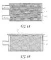
- FIGS. 1 a and 1 bare schematic top plan ( FIG. 1 a ) and side elevational ( FIG. 1 b ) views of a reactant trap comprising porous plates inside a suction box of an ALD reactor, constructed in accordance with a first preferred embodiment.
- FIGS. 2 a and 2 bare schematic top plan ( FIG. 2 a ) and side elevational ( FIG. 2 b ) views of a reactant trap, constructed in accordance with a second preferred embodiment of the present invention, having an arrangement of plates inside a separate postreactor connected to the suction box of an ALD reactor.
- FIGS. 3 a and 3 bare views corresponding to FIGS. 2 a and 2 b , with the plates replaced by glass wool cartridges, in accordance with a third embodiment.
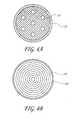
- FIGS. 4 a and 4 bare schematic cross-sections of a cartridge filled with glass wool ( FIG. 4 a ) and a cartridge filled with graphite foil ( FIG. 4 b ).
- the present inventionis based on the idea of placing—between the substrates of an ALD reactor and the pump—a material with a high surface area, which forms a postreaction substrate for the discharged superfluous gas phase reactants leaving the actual reaction zone. It is preferred that the surface of the porous material is so large that all of the superfluous material can adsorb upon surfaces of the reactant trap and then be converted into the corresponding final compound when the next reactant pulse enters, according to the principle of ALD (Atomic Layer Deposition).
- ALDAtomic Layer Deposition
- the postreaction reactant trapcan be placed inside the vacuum vessel, within the hot reaction zone, or it can be formed as a separate chamber between the process chamber (or primary reaction zone) and the pump; even the space of the suction box can be used as a holder for the trapping receptacles.
- the following examplerelates to growing an aluminum oxide layer with the ALD technique.
- 100 g of AlCl 3 and 100 g of H 2 Ois consumed.
- Roughly one-third (60 g) of the reactantsends up as Al 2 O 3 , of which aluminum represents 30 g and oxygen represents 30 g.
- Two-thirds of the consumed reactant masswill form HCl in an amount of 140 g.
- One-third, equaling 20 g of the precursors,is used in the thin film product grown on the substrates; the remaining two-thirds (40 g) of Al 2 O 3 is preferably captured by the trap. This means roughly 40 g of solids in the trap per run.
- the deposited Al 2 O 3 in each runhas a thickness of 150 nm, which corresponds to a film growth of 15 ⁇ m on the trap surface after 100 runs.
- the sacrificial trapping block(s) or platescan be made of any suitable material with a high surface area, preferably porous (e.g., graphite, such as porous graphite foils, alumina (Al2O3) or silica).
- porouse.g., graphite, such as porous graphite foils, alumina (Al2O3) or silica.
- ceramic materialse.g., honeycomb ceramics, and other mineral materials such as glass wool, can also be used.
- Reticulated Vitreous Carbonis another example of a suitable material.
- the materialshould withstand the physical and chemical conditions of the reaction zone (reaction temperature and pressure; it should be chemically inert to the reactants but able to adsorb the ALD reactants).
- the surface area of the trap materialis 10 m 2 /g to 2000 m 2 /g, in particular about 100 m 2 /g to 1500 m 2 /g.
- One alternativeis to have a porous ceramic material with a roughened surface which will allow for penetration of the gaseous reactants into the material, leaving by-products such as hydrochloric acid, on the surface so that it can be more easily purged away.
- the pores of the porous materialshould not be too narrow and deep so that the (non-reacted) residues of the previous pulse cannot be purged away before the next pulse is introduced. Material having an average pore size on the order of about 10 to 1000 m is preferred.
- the surface of the reactant trapis large enough that the same trap material can be used for the growth of several batches of thin-film elements.
- the excess of reactantis generally 4 to 5 times the amount needed for covering the surface of the substrates with a thin film of desired thickness. Therefore, the surface area of the material is preferably at least 4 to 5 times larger than the total surface of the substrates. More preferably, the surface should be much larger, e.g., so as to allow for uninterrupted operation for a whole day, depending on the production capacity of the reactor.
- the material with a high surface areais preferably provided with flow paths which allow for free flow of the gases while offering the gas phase components enough surface for surface reactions.
- flow pathswhich allow for free flow of the gases while offering the gas phase components enough surface for surface reactions.
- the reactant trap 1(which can also be called an “afterburner”, a “downstream reaction space” or a “secondary reaction space”) is preferably placed below the actual reaction space 2 (or “primary reaction space”) of the ALD reactor.
- the reactant trapcomprises a plurality of trapping plates 3 , which are placed in parallel relationship inside the suction box 4 of the reactor. Between the trapping plates 3 there are flow channels formed to allow for the continued flow of the gases to the pump (not shown).
- the trapping platesare made of a suitable material with a high surface area, the reactant gases will diffuse inside the plates and deposit the reactants due to surface reactions similar to those reactions taking place in the reaction space above, e.g., between glass substrates and the reactant vapors.
- the reaction spaceis generally purged with an inert or inactive gas, such as nitrogen. Then a subsequent gas phase pulse is fed into the reaction space (and thence into the reactant trap).
- an aluminum chloride pulseis usually followed by a water vapor pulse in the reaction space to convert the aluminum chloride into aluminum oxide.
- the same reactiontakes place on the surface of the substrates placed in the ALD reactor and in the reactant trap.
- the reactant trapBy placing the reactant trap inside the same reaction space or reaction box as the substrates, the necessary temperature and pressure levels for achieving an ALD (Atomic Layer Deposition) reaction on the surface of the trapping material are automatically obtained.
- the reactantswill form the same end product, e.g., ATO or Al 2 O 3 , on the surface of the trap as on the substrates.
- FIGS. 2 a and 2 bThe embodiment of FIGS. 2 a and 2 b is similar to that of FIGS. 1 a and 1 b , with the exception that the reactant trap 11 is placed in a separate vessel 13 kept at the same reaction conditions as the reactor.
- the trapping plates 12are arranged in a similar fashion as the plates in FIGS. 1 a and 1 b , but the flow channel is arranged to provide a serpentine path. In this way, a sufficient contact time with the trapping plates can be provided.
- the reactant trap vesselis attached to the suction box of an ALD reactor with a conduit.
- FIGS. 3 a and 3 bcorresponds to a combination of the embodiment of FIGS. 1 and 2 , in the sense that the trapping plates 22 are placed in a separate vessel 23 , but the plates are fixed in parallel relationship with flow paths between them.
- the plates 22 of the illustrated embodimentare made of glass wool.
- FIGS. 4 a and 4 bshow replaceable cartridges 32 made of material with a high surface area, such as glass wool ( FIG. 4 a ) with flow paths 33 formed in said material. Similar flow paths 35 are arranged between adjacent layers of a graphite foil 34 wound in a spiral fashion in FIG. 4 b .
- the layersare preferably arranged at a distance of about 0.1 mm to 10 mm, preferably about 0.5 mm to 5 mm from each other.
- the traps of FIGS. 4 a and 4 bare preferably made of an inexpensive material, such that they can be thrown away after an effective period of use.
- the operation of the precursor trapis quite similar to that described in connection with the embodiment of FIGS. 1 a and 1 b .
- the material with a high surface areais maintained at a temperature similar to that of the actual reaction zone (i.e., depending on the precursors and the substrate, preferably about a 50° C. to 600° C., more preferably about 200° C. to 500° C.).
- the pressurecan be atmospheric, but it is generally preferred to work at reduced pressure of about 1 mbar to 100 mbar (i.e., “low pressure”).
- the inactive gas used for purgingpreferably comprises nitrogen or a noble gas such as argon.
Landscapes
- Engineering & Computer Science (AREA)
- Chemical & Material Sciences (AREA)
- Health & Medical Sciences (AREA)
- Biomedical Technology (AREA)
- Environmental & Geological Engineering (AREA)
- Analytical Chemistry (AREA)
- General Chemical & Material Sciences (AREA)
- Oil, Petroleum & Natural Gas (AREA)
- Chemical Kinetics & Catalysis (AREA)
- Chemical Vapour Deposition (AREA)
- Treating Waste Gases (AREA)
- Physical Or Chemical Processes And Apparatus (AREA)
Abstract
Description
This application is a continuation of application Ser. No. 10/205,296, filed Jul. 24, 2002, which is a continuation of U.S. patent application Ser. No. 09/619,820, filed Jul. 20, 2000, which claims the priority benefit under 35 U.S.C. §119 of prior Finnish Application No. 991628, filed Jul. 20, 1999.
1. Field of the Invention
The present invention relates to the removal of substances contained in gases, such as gases flowing at low pressure. In particular, the present invention concerns a method and an apparatus for removing unreacted reactants and vapor phase precursors present in gases removed from vapor phase reactors.
2. Description of the Related Art
In the atomic layer deposition method (ALD), the substrate is typically located in a reaction space, wherein it is subjected to alternately repeated surface reactions of at least two different reactants. Commercially available technology is supplied by ASM Microchemistry Oy, Espoo Finland under the trademark ALCVD™. According to the method, the reactants are admitted repetitively and alternately one reactant at a time from its own source in the form of vapor-phase pulses in the reaction space. Here, the vapor-phase reactants are allowed to react with the substrate surface for the purpose of forming a solid-state thin film on the substrate, particularly for use in the semiconductor arts.
While the method is most appropriately suited for producing so-called compound thin films, using as the reactants starting materials or precursors that contain component elements of the desired compound thin-film, it may also be applied to growing elemental thin films. Of compound films typically used in the art, reference can be made to ZnS films employed in electroluminescent displays, whereby such films are grown on a glass substrate using zinc sulfide and hydrogen sulfide as the reactants in the growth process. Of elemental thin films, reference can be made to silicon thin films.
An ALD apparatus comprises a reaction space into which the substrate can be placed, and at least two reactant sources from which the reactants used in the thin-film growth process can be fed in the form of vapor-phase pulses into the reaction space. The sources are connected to the reaction space via reactant inflow channels. Outflow channels (pumping lines) are attached to a pump and connected to the reaction space for removing the gaseous reaction products of the thin-film growth process, as well as the excess reactants in vapor phase.
The waste, i.e., the non-reacted reactants removed and discharged from the reaction space, is a serious problem for ALD processing. When it enters the pumping line and the pump, the waste gives rise to tedious cleaning and, in the worst case, the pump will rapidly be worn out.
Filtering of the gases and/or contacting of the gases with absorbents gives some help but both methods have been shown to be unsatisfactory in the long run. Building expensive heated pumping lines in order to move the waste though the pump does not help, because the problematic waste does not comprise superfluous amounts of separate precursors, such as water, titanium chloride or aluminum chloride, that can easily be pumped as separate materials. The problem arises when the materials are reacting, forming by-products having a lower vapor pressure, inside the pumping line. The problem is especially relevant when the reactants react with each other at temperatures lower than the intended process temperature, causing improper reactions. At those temperatures, oxychlorides might form in exhaust lines as a by-product of exemplary metal oxide deposition processes using metal chlorides as one of the ALD precursors. These by-products form a high volume powder. Typically this kind of reaction happens inside the pumping line between the reaction zone and the colder parts of the pumping line. Another problem occurs when precursors with a high vapor pressure at room temperature reach the pump sequentially at temperatures suitable for film growth. This might lead to a film material build-up on the surfaces of the pump. The material build-up can be very abrasive. This is a specific problem with heated pumping lines and hot dry pumps. This will cause the filling of tight tolerances and due to that the parts will contact each other and pump will crash. A third problem is the reactions between condensed portions of the previous reaction component and the vapor of the following pulse in the pumping line. This will cause CVD-type material growth and significant powder propagation.
As mentioned above, different solutions based on filtering and/or chemical treatment of the reaction waste have been tried for decades in process fore-lines, with more or less poor results. Formed by-products and powder tend to block the filters and due to the low process pressure the gas flow is too weak to keep the mesh of the filter open. The blocked filter will cause an additional pressure drop and therefore cause changes in the material flow from the source. Also, the process pressure and the speed of the gases will change. Attempts have been made to use cyclones and rotating peelers to remove the by-products from the mesh. By these means, some of the solid waste can be removed, but still the precursors with high vapor pressure will reach the pump and form by-products there.
Finnish Patent No. 84980 (Planar International Oy) discloses a system consisting of a condensation chamber, where the gas stream is slowed down and where a big part of the waste is condensed. Before entering the filter unit, extra water is injected into the filter housing to increase the by-products' particle size in order to prevent blockage of the filter mesh before the waste is removed by a rotating peeler system. Although this apparatus represents a clear improvement of the state of the art, it is still not completely satisfactory.
It is an aim of the present invention to eliminate the problem of the prior art and to provide a simple and reliable technical solution for removing waste from the reaction zone of an ALD reactor.
The present invention is based on the concept of processing all of the extra precursor material of the pulse dose, to form the end product, before the precursors are discharged from the reactor or the reaction zone. Thereby, the volume of the waste can be greatly reduced. The postprocessing of the precursor excess stemming from the ALD process is carried out by placing a sacrificial material with a high surface area (typically porous) in the reaction zone, which is swept by the precursors during their travel to the outlet of the reaction chamber. Alternatively, the material with high surface area can be placed in a separate heated vessel, outside the reaction zone but upstream of the discharge pump. The material with a high surface area is, however, in both embodiments kept essentially the growth conditions (for example, same pressure and temperature) as the reaction zone to ensure growth of a reaction product on the surface thereof. As a result, the material with a high surface area traps the remaining end product on its surface, thereby reducing the amount of reactant reaching the pump.
The present apparatus includes a reaction zone arranged downstream from (i.e., after) the reaction process, comprising a material with a high surface area and maintainable at essentially the same conditions as those prevailing during the gas phase reaction process. The reaction zone further includes gas flow channels for feeding gases discharged from the gas phase reaction process into the material with a high surface area and discharge gas channels for discharging gas from the material with a high surface area.
Considerable advantages are obtained with the present invention. Thus, the material with a high surface area will trap on its surface the end product of the reaction of the excess gaseous reactants. The surface area of the trap is generally large, on an average about 10 m2/g to 1000 m2/g; for example it can have the surface area on the same order as that of a soccer stadium. The trap can be in use for several runs before it is cleaned or replaced with a new one. The pump connected to the reaction space has only to cope with materials in gaseous form because mostly non-reactive gaseous by-products from the process reach the pump. “Non-reactive,” as used herein, refers to species other than the intended ALD reactants. The solid thin film product is substantially captured in the reactant trap; this will considerably reduce wear of the equipment.
The present invention is generally applicable to any gaseous reactants. It is particularly advantageous for reactions that form corrosive or otherwise harmful side products during the reaction of the gaseous reactants. Thus, a preferred embodiment is for dealing with the waste generated in a vapor phase reaction using chloride-containing reactants such as aluminum chloride, which are reacted with water to produce a metal oxide. The present invention is preferably used for ALD, but it can also be used for treating exhaust from conventional CVD processing or electron beam sputtering and any other gas phase processes in which the discharged gaseous reactants may react with each other downstream of the actual reaction zone housing the substrate. In the following description, the invention will, however, be described with particular reference to an ALD embodiment.
Next the invention will be examined in more detail with reference to the attached drawings depicting a number of preferred embodiments.
Generally, the present invention is based on the idea of placing—between the substrates of an ALD reactor and the pump—a material with a high surface area, which forms a postreaction substrate for the discharged superfluous gas phase reactants leaving the actual reaction zone. It is preferred that the surface of the porous material is so large that all of the superfluous material can adsorb upon surfaces of the reactant trap and then be converted into the corresponding final compound when the next reactant pulse enters, according to the principle of ALD (Atomic Layer Deposition).
The postreaction reactant trap can be placed inside the vacuum vessel, within the hot reaction zone, or it can be formed as a separate chamber between the process chamber (or primary reaction zone) and the pump; even the space of the suction box can be used as a holder for the trapping receptacles.
The following example relates to growing an aluminum oxide layer with the ALD technique. In a 3,000 cycle Al2O3process, 100 g of AlCl3and 100 g of H2O is consumed. Roughly one-third (60 g) of the reactants ends up as Al2O3, of which aluminum represents 30 g and oxygen represents 30 g. Two-thirds of the consumed reactant mass will form HCl in an amount of 140 g. One-third, equaling 20 g of the precursors, is used in the thin film product grown on the substrates; the remaining two-thirds (40 g) of Al2O3is preferably captured by the trap. This means roughly 40 g of solids in the trap per run. The deposited Al2O3in each run has a thickness of 150 nm, which corresponds to a film growth of 15 μm on the trap surface after 100 runs. By selecting the pore size and path length so that there is essentially no pressure drop over the trap and that any reaction products can be purged away before the next pulse enters the trap, the thin film grown in the trap will not restrict the gas flow.
It is particularly desirable to avoid formation of large molecules, such as oxychlorides, that would occupy a large volume and block the flow paths of the material with a high surface area.
According to the preferred embodiment, the sacrificial trapping block(s) or plates can be made of any suitable material with a high surface area, preferably porous (e.g., graphite, such as porous graphite foils, alumina (Al2O3) or silica). Various ceramic materials, e.g., honeycomb ceramics, and other mineral materials such as glass wool, can also be used. Reticulated Vitreous Carbon is another example of a suitable material. The material should withstand the physical and chemical conditions of the reaction zone (reaction temperature and pressure; it should be chemically inert to the reactants but able to adsorb the ALD reactants). Further it should have a large surface so as to allow for a reaction of the gaseous reactants on the surface thereof in order to form the reaction product (such as aluminum oxide). Generally, the surface area of the trap material is 10 m2/g to 2000 m2/g, in particular about 100 m2/g to 1500 m2/g. One alternative is to have a porous ceramic material with a roughened surface which will allow for penetration of the gaseous reactants into the material, leaving by-products such as hydrochloric acid, on the surface so that it can be more easily purged away. The pores of the porous material should not be too narrow and deep so that the (non-reacted) residues of the previous pulse cannot be purged away before the next pulse is introduced. Material having an average pore size on the order of about 10 to 1000 m is preferred.
It is also preferred that the surface of the reactant trap is large enough that the same trap material can be used for the growth of several batches of thin-film elements. As discussed above, the excess of reactant is generally 4 to 5 times the amount needed for covering the surface of the substrates with a thin film of desired thickness. Therefore, the surface area of the material is preferably at least 4 to 5 times larger than the total surface of the substrates. More preferably, the surface should be much larger, e.g., so as to allow for uninterrupted operation for a whole day, depending on the production capacity of the reactor.
There should be no substantial pressure difference over the high surface area of the reactant trap. For this reason, the material with a high surface area is preferably provided with flow paths which allow for free flow of the gases while offering the gas phase components enough surface for surface reactions. Various ways of achieving free flow paths to achieve minimal pressure drops are depicted in the embodiments of the drawings.
Turning now to the attached drawings, it will be noted that inFIGS. 1 aand1b, the reactant trap1 (which can also be called an “afterburner”, a “downstream reaction space” or a “secondary reaction space”) is preferably placed below the actual reaction space2 (or “primary reaction space”) of the ALD reactor. The reactant trap comprises a plurality of trappingplates 3, which are placed in parallel relationship inside the suction box4 of the reactor. Between thetrapping plates 3 there are flow channels formed to allow for the continued flow of the gases to the pump (not shown). When the trapping plates are made of a suitable material with a high surface area, the reactant gases will diffuse inside the plates and deposit the reactants due to surface reactions similar to those reactions taking place in the reaction space above, e.g., between glass substrates and the reactant vapors.
By arranging the reactant trap immediately after or under the reaction zone, a free flow path or channel for the excess reactants can easily be arranged. Likewise, it is simple to carry out the discharge of the gas from the reactant trap because it is subject to the same reduced pressure, produced by the discharge pump, as the rest of the reactor.
After each reactant pulse fed in to the reaction space and, consequently, into the reactant trap1, the reaction space is generally purged with an inert or inactive gas, such as nitrogen. Then a subsequent gas phase pulse is fed into the reaction space (and thence into the reactant trap). Thus, in the example of an ALD Al2O3process, an aluminum chloride pulse is usually followed by a water vapor pulse in the reaction space to convert the aluminum chloride into aluminum oxide. The same reaction takes place on the surface of the substrates placed in the ALD reactor and in the reactant trap. By placing the reactant trap inside the same reaction space or reaction box as the substrates, the necessary temperature and pressure levels for achieving an ALD (Atomic Layer Deposition) reaction on the surface of the trapping material are automatically obtained. The reactants will form the same end product, e.g., ATO or Al2O3, on the surface of the trap as on the substrates.
The embodiment ofFIGS. 2 aand2bis similar to that ofFIGS. 1 aand1b, with the exception that thereactant trap 11 is placed in aseparate vessel 13 kept at the same reaction conditions as the reactor. The trappingplates 12 are arranged in a similar fashion as the plates inFIGS. 1 aand1b, but the flow channel is arranged to provide a serpentine path. In this way, a sufficient contact time with the trapping plates can be provided. The reactant trap vessel is attached to the suction box of an ALD reactor with a conduit.
The embodiment ofFIGS. 3 aand3bcorresponds to a combination of the embodiment ofFIGS. 1 and 2 , in the sense that the trappingplates 22 are placed in aseparate vessel 23, but the plates are fixed in parallel relationship with flow paths between them. Theplates 22 of the illustrated embodiment are made of glass wool.
The traps ofFIGS. 4 aand4bare preferably made of an inexpensive material, such that they can be thrown away after an effective period of use.
In the embodiments of all of theFIGS. 2 to 4 , the operation of the precursor trap is quite similar to that described in connection with the embodiment ofFIGS. 1 aand1b. The material with a high surface area is maintained at a temperature similar to that of the actual reaction zone (i.e., depending on the precursors and the substrate, preferably about a 50° C. to 600° C., more preferably about 200° C. to 500° C.). The pressure can be atmospheric, but it is generally preferred to work at reduced pressure of about 1 mbar to 100 mbar (i.e., “low pressure”). The inactive gas used for purging preferably comprises nitrogen or a noble gas such as argon.
Although the above embodiments have particular utility in the preparation of thin-film structures on all kinds of surfaces for semiconductor and flat panel devices, it should be noted that it can be applied to any chemical gas vapor deposition reactor (e.g., CVD or ALD), including the preparation of catalysts using thin film coatings.
Claims (14)
1. A method for removing substances contained in exhaust gases discharged from gas phase reaction processes, comprising:
carrying excess reactant from gas phase pulses of an atomic layer deposition (ALD) process conducted upon a deposition substrate under a first set of reaction conditions; and
directing the excess reactant to contact a sacrificial material downstream of the substrate and maintained at substantially the first set of reaction conditions.
2. The method ofclaim 1 , wherein the sacrificial material comprises a porous substrate.
3. The method ofclaim 2 , wherein directing comprises conducting the ALD process on the sacrificial material to leave a sacrificial layer having a composition that is substantially the same as a layer formed by the ALD process upon the deposition substrate.
4. The method ofclaim 2 , wherein the porous material comprises a material selected from the group consisting of porous graphite materials, porous ceramics, alumina, silica and glass wool.
5. The method ofclaim 1 , wherein the excess reactant includes a halide-containing gas.
6. The method ofclaim 5 , wherein the halide-containing gas comprises a chloride-containing gas.
7. The method ofclaim 1 , wherein the substrate and the sacrificial material are maintained within a single reaction space.
8. The method ofclaim 1 , wherein the sacrificial material is placed in a downstream reaction space housing that is connected to an upstream reaction space housing the substrate.
9. The method ofclaim 1 , wherein the sacrificial material has a surface area between about 10 m2/g and 2000 m2/g.
10. The method ofclaim 1 , wherein at the first set of conditions the deposition substrate and sacrificial material are at a temperature between about 200° C. and 500° C.
11. The method ofclaim 10 , wherein at the first set of conditions the deposition substrate and the sacrificial material are subjected to a pressure between about 1 mbar and 100 mbar.
12. The method ofclaim 1 , wherein the sacrificial material has a surface area sufficient to react substantially all of the excess reactant.
13. The method ofclaim 1 , wherein the sacrificial material comprises a porous material having an average pore size of about 10 μm to 100 μm.
14. A method of depleting excess reactant from an exhaust flow, comprising:
reacting a first part of a gaseous reactant with at least one substrate within a primary reaction space, wherein said reacting comprises an atomic layer deposition (ALD) process;
exhausting an excess part of the gaseous reactant that not reacted with said at least one substrate to a secondary reaction space downstream of the primary reaction space, said secondary reaction space being maintained at a set of conditions substantially the same as those prevailing in the primary reaction space during said reacting of the first part of the gaseous reactant;
further reacting the excess part of the gaseous reactant with a sacrificial material having a high surface area, wherein said further reacting comprises an ALD process; and
exhausting by-product from the secondary reaction space, said by-product comprising by-product from said first reacting of the first past of the gaseous material and by-product from said further reacting of the excess part of the gaseous material.
Priority Applications (1)
| Application Number | Priority Date | Filing Date | Title |
|---|---|---|---|
| US12/138,358US7799300B2 (en) | 1999-07-20 | 2008-06-12 | Method and apparatus for removing substances from gases |
Applications Claiming Priority (5)
| Application Number | Priority Date | Filing Date | Title |
|---|---|---|---|
| FI991628AFI110311B (en) | 1999-07-20 | 1999-07-20 | Method and apparatus for eliminating substances from gases |
| FI991628 | 1999-07-20 | ||
| US09/619,820US6506352B1 (en) | 1999-07-20 | 2000-07-20 | Method for removing substances from gases |
| US10/205,296US20020187084A1 (en) | 1999-07-20 | 2002-07-24 | Method and apparatus for removing substances from gases |
| US12/138,358US7799300B2 (en) | 1999-07-20 | 2008-06-12 | Method and apparatus for removing substances from gases |
Related Parent Applications (1)
| Application Number | Title | Priority Date | Filing Date |
|---|---|---|---|
| US10/205,296ContinuationUS20020187084A1 (en) | 1999-07-20 | 2002-07-24 | Method and apparatus for removing substances from gases |
Publications (2)
| Publication Number | Publication Date |
|---|---|
| US20090074964A1 US20090074964A1 (en) | 2009-03-19 |
| US7799300B2true US7799300B2 (en) | 2010-09-21 |
Family
ID=8555096
Family Applications (3)
| Application Number | Title | Priority Date | Filing Date |
|---|---|---|---|
| US09/619,820Expired - LifetimeUS6506352B1 (en) | 1999-07-20 | 2000-07-20 | Method for removing substances from gases |
| US10/205,296AbandonedUS20020187084A1 (en) | 1999-07-20 | 2002-07-24 | Method and apparatus for removing substances from gases |
| US12/138,358Expired - Fee RelatedUS7799300B2 (en) | 1999-07-20 | 2008-06-12 | Method and apparatus for removing substances from gases |
Family Applications Before (2)
| Application Number | Title | Priority Date | Filing Date |
|---|---|---|---|
| US09/619,820Expired - LifetimeUS6506352B1 (en) | 1999-07-20 | 2000-07-20 | Method for removing substances from gases |
| US10/205,296AbandonedUS20020187084A1 (en) | 1999-07-20 | 2002-07-24 | Method and apparatus for removing substances from gases |
Country Status (4)
| Country | Link |
|---|---|
| US (3) | US6506352B1 (en) |
| JP (1) | JP2001062244A (en) |
| FI (1) | FI110311B (en) |
| TW (1) | TW555585B (en) |
Cited By (298)
| Publication number | Priority date | Publication date | Assignee | Title |
|---|---|---|---|---|
| US10720331B2 (en) | 2016-11-01 | 2020-07-21 | ASM IP Holdings, B.V. | Methods for forming a transition metal nitride film on a substrate by atomic layer deposition and related semiconductor device structures |
| US10767789B2 (en) | 2018-07-16 | 2020-09-08 | Asm Ip Holding B.V. | Diaphragm valves, valve components, and methods for forming valve components |
| US10784102B2 (en) | 2016-12-22 | 2020-09-22 | Asm Ip Holding B.V. | Method of forming a structure on a substrate |
| US10787741B2 (en) | 2014-08-21 | 2020-09-29 | Asm Ip Holding B.V. | Method and system for in situ formation of gas-phase compounds |
| US10797133B2 (en) | 2018-06-21 | 2020-10-06 | Asm Ip Holding B.V. | Method for depositing a phosphorus doped silicon arsenide film and related semiconductor device structures |
| US10804098B2 (en) | 2009-08-14 | 2020-10-13 | Asm Ip Holding B.V. | Systems and methods for thin-film deposition of metal oxides using excited nitrogen-oxygen species |
| US10818758B2 (en) | 2018-11-16 | 2020-10-27 | Asm Ip Holding B.V. | Methods for forming a metal silicate film on a substrate in a reaction chamber and related semiconductor device structures |
| US10829852B2 (en) | 2018-08-16 | 2020-11-10 | Asm Ip Holding B.V. | Gas distribution device for a wafer processing apparatus |
| US10832903B2 (en) | 2011-10-28 | 2020-11-10 | Asm Ip Holding B.V. | Process feed management for semiconductor substrate processing |
| US10847366B2 (en) | 2018-11-16 | 2020-11-24 | Asm Ip Holding B.V. | Methods for depositing a transition metal chalcogenide film on a substrate by a cyclical deposition process |
| US10844486B2 (en) | 2009-04-06 | 2020-11-24 | Asm Ip Holding B.V. | Semiconductor processing reactor and components thereof |
| US10847371B2 (en) | 2018-03-27 | 2020-11-24 | Asm Ip Holding B.V. | Method of forming an electrode on a substrate and a semiconductor device structure including an electrode |
| US10844484B2 (en) | 2017-09-22 | 2020-11-24 | Asm Ip Holding B.V. | Apparatus for dispensing a vapor phase reactant to a reaction chamber and related methods |
| US10851456B2 (en) | 2016-04-21 | 2020-12-01 | Asm Ip Holding B.V. | Deposition of metal borides |
| US10858737B2 (en) | 2014-07-28 | 2020-12-08 | Asm Ip Holding B.V. | Showerhead assembly and components thereof |
| US10865475B2 (en) | 2016-04-21 | 2020-12-15 | Asm Ip Holding B.V. | Deposition of metal borides and silicides |
| US10867786B2 (en) | 2018-03-30 | 2020-12-15 | Asm Ip Holding B.V. | Substrate processing method |
| US10867788B2 (en) | 2016-12-28 | 2020-12-15 | Asm Ip Holding B.V. | Method of forming a structure on a substrate |
| US10872771B2 (en) | 2018-01-16 | 2020-12-22 | Asm Ip Holding B. V. | Method for depositing a material film on a substrate within a reaction chamber by a cyclical deposition process and related device structures |
| US10886123B2 (en) | 2017-06-02 | 2021-01-05 | Asm Ip Holding B.V. | Methods for forming low temperature semiconductor layers and related semiconductor device structures |
| US10883175B2 (en) | 2018-08-09 | 2021-01-05 | Asm Ip Holding B.V. | Vertical furnace for processing substrates and a liner for use therein |
| US10892156B2 (en) | 2017-05-08 | 2021-01-12 | Asm Ip Holding B.V. | Methods for forming a silicon nitride film on a substrate and related semiconductor device structures |
| US10896820B2 (en) | 2018-02-14 | 2021-01-19 | Asm Ip Holding B.V. | Method for depositing a ruthenium-containing film on a substrate by a cyclical deposition process |
| US10910262B2 (en) | 2017-11-16 | 2021-02-02 | Asm Ip Holding B.V. | Method of selectively depositing a capping layer structure on a semiconductor device structure |
| US10914004B2 (en) | 2018-06-29 | 2021-02-09 | Asm Ip Holding B.V. | Thin-film deposition method and manufacturing method of semiconductor device |
| US10923344B2 (en) | 2017-10-30 | 2021-02-16 | Asm Ip Holding B.V. | Methods for forming a semiconductor structure and related semiconductor structures |
| US10928731B2 (en) | 2017-09-21 | 2021-02-23 | Asm Ip Holding B.V. | Method of sequential infiltration synthesis treatment of infiltrateable material and structures and devices formed using same |
| US10934619B2 (en) | 2016-11-15 | 2021-03-02 | Asm Ip Holding B.V. | Gas supply unit and substrate processing apparatus including the gas supply unit |
| US10941490B2 (en) | 2014-10-07 | 2021-03-09 | Asm Ip Holding B.V. | Multiple temperature range susceptor, assembly, reactor and system including the susceptor, and methods of using the same |
| US10943771B2 (en) | 2016-10-26 | 2021-03-09 | Asm Ip Holding B.V. | Methods for thermally calibrating reaction chambers |
| US10950432B2 (en) | 2017-04-25 | 2021-03-16 | Asm Ip Holding B.V. | Method of depositing thin film and method of manufacturing semiconductor device |
| USD913980S1 (en) | 2018-02-01 | 2021-03-23 | Asm Ip Holding B.V. | Gas supply plate for semiconductor manufacturing apparatus |
| US10975470B2 (en) | 2018-02-23 | 2021-04-13 | Asm Ip Holding B.V. | Apparatus for detecting or monitoring for a chemical precursor in a high temperature environment |
| US11001925B2 (en) | 2016-12-19 | 2021-05-11 | Asm Ip Holding B.V. | Substrate processing apparatus |
| US11004977B2 (en) | 2017-07-19 | 2021-05-11 | Asm Ip Holding B.V. | Method for depositing a group IV semiconductor and related semiconductor device structures |
| US11018047B2 (en) | 2018-01-25 | 2021-05-25 | Asm Ip Holding B.V. | Hybrid lift pin |
| US11015245B2 (en) | 2014-03-19 | 2021-05-25 | Asm Ip Holding B.V. | Gas-phase reactor and system having exhaust plenum and components thereof |
| US11018002B2 (en) | 2017-07-19 | 2021-05-25 | Asm Ip Holding B.V. | Method for selectively depositing a Group IV semiconductor and related semiconductor device structures |
| US11022879B2 (en) | 2017-11-24 | 2021-06-01 | Asm Ip Holding B.V. | Method of forming an enhanced unexposed photoresist layer |
| US11024523B2 (en) | 2018-09-11 | 2021-06-01 | Asm Ip Holding B.V. | Substrate processing apparatus and method |
| US11031242B2 (en) | 2018-11-07 | 2021-06-08 | Asm Ip Holding B.V. | Methods for depositing a boron doped silicon germanium film |
| USD922229S1 (en) | 2019-06-05 | 2021-06-15 | Asm Ip Holding B.V. | Device for controlling a temperature of a gas supply unit |
| US11049751B2 (en) | 2018-09-14 | 2021-06-29 | Asm Ip Holding B.V. | Cassette supply system to store and handle cassettes and processing apparatus equipped therewith |
| US11056344B2 (en) | 2017-08-30 | 2021-07-06 | Asm Ip Holding B.V. | Layer forming method |
| US11053591B2 (en) | 2018-08-06 | 2021-07-06 | Asm Ip Holding B.V. | Multi-port gas injection system and reactor system including same |
| US11056567B2 (en) | 2018-05-11 | 2021-07-06 | Asm Ip Holding B.V. | Method of forming a doped metal carbide film on a substrate and related semiconductor device structures |
| US11069510B2 (en) | 2017-08-30 | 2021-07-20 | Asm Ip Holding B.V. | Substrate processing apparatus |
| US11081345B2 (en) | 2018-02-06 | 2021-08-03 | Asm Ip Holding B.V. | Method of post-deposition treatment for silicon oxide film |
| US11088002B2 (en) | 2018-03-29 | 2021-08-10 | Asm Ip Holding B.V. | Substrate rack and a substrate processing system and method |
| US11087997B2 (en) | 2018-10-31 | 2021-08-10 | Asm Ip Holding B.V. | Substrate processing apparatus for processing substrates |
| US11094546B2 (en) | 2017-10-05 | 2021-08-17 | Asm Ip Holding B.V. | Method for selectively depositing a metallic film on a substrate |
| US11094582B2 (en) | 2016-07-08 | 2021-08-17 | Asm Ip Holding B.V. | Selective deposition method to form air gaps |
| US11101370B2 (en) | 2016-05-02 | 2021-08-24 | Asm Ip Holding B.V. | Method of forming a germanium oxynitride film |
| US11107676B2 (en) | 2016-07-28 | 2021-08-31 | Asm Ip Holding B.V. | Method and apparatus for filling a gap |
| US11114294B2 (en) | 2019-03-08 | 2021-09-07 | Asm Ip Holding B.V. | Structure including SiOC layer and method of forming same |
| US11114283B2 (en) | 2018-03-16 | 2021-09-07 | Asm Ip Holding B.V. | Reactor, system including the reactor, and methods of manufacturing and using same |
| USD930782S1 (en) | 2019-08-22 | 2021-09-14 | Asm Ip Holding B.V. | Gas distributor |
| US11127617B2 (en) | 2017-11-27 | 2021-09-21 | Asm Ip Holding B.V. | Storage device for storing wafer cassettes for use with a batch furnace |
| US11127589B2 (en) | 2019-02-01 | 2021-09-21 | Asm Ip Holding B.V. | Method of topology-selective film formation of silicon oxide |
| USD931978S1 (en) | 2019-06-27 | 2021-09-28 | Asm Ip Holding B.V. | Showerhead vacuum transport |
| US11139191B2 (en) | 2017-08-09 | 2021-10-05 | Asm Ip Holding B.V. | Storage apparatus for storing cassettes for substrates and processing apparatus equipped therewith |
| US11139308B2 (en) | 2015-12-29 | 2021-10-05 | Asm Ip Holding B.V. | Atomic layer deposition of III-V compounds to form V-NAND devices |
| US11158513B2 (en) | 2018-12-13 | 2021-10-26 | Asm Ip Holding B.V. | Methods for forming a rhenium-containing film on a substrate by a cyclical deposition process and related semiconductor device structures |
| US11164955B2 (en) | 2017-07-18 | 2021-11-02 | Asm Ip Holding B.V. | Methods for forming a semiconductor device structure and related semiconductor device structures |
| US11171025B2 (en) | 2019-01-22 | 2021-11-09 | Asm Ip Holding B.V. | Substrate processing device |
| USD935572S1 (en) | 2019-05-24 | 2021-11-09 | Asm Ip Holding B.V. | Gas channel plate |
| US11168395B2 (en) | 2018-06-29 | 2021-11-09 | Asm Ip Holding B.V. | Temperature-controlled flange and reactor system including same |
| US11205585B2 (en) | 2016-07-28 | 2021-12-21 | Asm Ip Holding B.V. | Substrate processing apparatus and method of operating the same |
| US11217444B2 (en) | 2018-11-30 | 2022-01-04 | Asm Ip Holding B.V. | Method for forming an ultraviolet radiation responsive metal oxide-containing film |
| USD940837S1 (en) | 2019-08-22 | 2022-01-11 | Asm Ip Holding B.V. | Electrode |
| US11222772B2 (en) | 2016-12-14 | 2022-01-11 | Asm Ip Holding B.V. | Substrate processing apparatus |
| US11227789B2 (en) | 2019-02-20 | 2022-01-18 | Asm Ip Holding B.V. | Method and apparatus for filling a recess formed within a substrate surface |
| US11227782B2 (en) | 2019-07-31 | 2022-01-18 | Asm Ip Holding B.V. | Vertical batch furnace assembly |
| US11233133B2 (en) | 2015-10-21 | 2022-01-25 | Asm Ip Holding B.V. | NbMC layers |
| US11232963B2 (en) | 2018-10-03 | 2022-01-25 | Asm Ip Holding B.V. | Substrate processing apparatus and method |
| US11230766B2 (en) | 2018-03-29 | 2022-01-25 | Asm Ip Holding B.V. | Substrate processing apparatus and method |
| US11242598B2 (en) | 2015-06-26 | 2022-02-08 | Asm Ip Holding B.V. | Structures including metal carbide material, devices including the structures, and methods of forming same |
| US11251040B2 (en) | 2019-02-20 | 2022-02-15 | Asm Ip Holding B.V. | Cyclical deposition method including treatment step and apparatus for same |
| US11251068B2 (en) | 2018-10-19 | 2022-02-15 | Asm Ip Holding B.V. | Substrate processing apparatus and substrate processing method |
| USD944946S1 (en) | 2019-06-14 | 2022-03-01 | Asm Ip Holding B.V. | Shower plate |
| US11270899B2 (en) | 2018-06-04 | 2022-03-08 | Asm Ip Holding B.V. | Wafer handling chamber with moisture reduction |
| US11274369B2 (en) | 2018-09-11 | 2022-03-15 | Asm Ip Holding B.V. | Thin film deposition method |
| US11282698B2 (en) | 2019-07-19 | 2022-03-22 | Asm Ip Holding B.V. | Method of forming topology-controlled amorphous carbon polymer film |
| US11286562B2 (en) | 2018-06-08 | 2022-03-29 | Asm Ip Holding B.V. | Gas-phase chemical reactor and method of using same |
| US11286558B2 (en) | 2019-08-23 | 2022-03-29 | Asm Ip Holding B.V. | Methods for depositing a molybdenum nitride film on a surface of a substrate by a cyclical deposition process and related semiconductor device structures including a molybdenum nitride film |
| US11289326B2 (en) | 2019-05-07 | 2022-03-29 | Asm Ip Holding B.V. | Method for reforming amorphous carbon polymer film |
| USD947913S1 (en) | 2019-05-17 | 2022-04-05 | Asm Ip Holding B.V. | Susceptor shaft |
| US11295980B2 (en) | 2017-08-30 | 2022-04-05 | Asm Ip Holding B.V. | Methods for depositing a molybdenum metal film over a dielectric surface of a substrate by a cyclical deposition process and related semiconductor device structures |
| USD948463S1 (en) | 2018-10-24 | 2022-04-12 | Asm Ip Holding B.V. | Susceptor for semiconductor substrate supporting apparatus |
| USD949319S1 (en) | 2019-08-22 | 2022-04-19 | Asm Ip Holding B.V. | Exhaust duct |
| US11306395B2 (en) | 2017-06-28 | 2022-04-19 | Asm Ip Holding B.V. | Methods for depositing a transition metal nitride film on a substrate by atomic layer deposition and related deposition apparatus |
| US11315794B2 (en) | 2019-10-21 | 2022-04-26 | Asm Ip Holding B.V. | Apparatus and methods for selectively etching films |
| US11342216B2 (en) | 2019-02-20 | 2022-05-24 | Asm Ip Holding B.V. | Cyclical deposition method and apparatus for filling a recess formed within a substrate surface |
| US11339476B2 (en) | 2019-10-08 | 2022-05-24 | Asm Ip Holding B.V. | Substrate processing device having connection plates, substrate processing method |
| US11345999B2 (en) | 2019-06-06 | 2022-05-31 | Asm Ip Holding B.V. | Method of using a gas-phase reactor system including analyzing exhausted gas |
| US11355338B2 (en) | 2019-05-10 | 2022-06-07 | Asm Ip Holding B.V. | Method of depositing material onto a surface and structure formed according to the method |
| US11361990B2 (en) | 2018-05-28 | 2022-06-14 | Asm Ip Holding B.V. | Substrate processing method and device manufactured by using the same |
| US11374112B2 (en) | 2017-07-19 | 2022-06-28 | Asm Ip Holding B.V. | Method for depositing a group IV semiconductor and related semiconductor device structures |
| US11378337B2 (en) | 2019-03-28 | 2022-07-05 | Asm Ip Holding B.V. | Door opener and substrate processing apparatus provided therewith |
| US11387120B2 (en) | 2017-09-28 | 2022-07-12 | Asm Ip Holding B.V. | Chemical dispensing apparatus and methods for dispensing a chemical to a reaction chamber |
| US11390945B2 (en) | 2019-07-03 | 2022-07-19 | Asm Ip Holding B.V. | Temperature control assembly for substrate processing apparatus and method of using same |
| US11390950B2 (en) | 2017-01-10 | 2022-07-19 | Asm Ip Holding B.V. | Reactor system and method to reduce residue buildup during a film deposition process |
| US11390946B2 (en) | 2019-01-17 | 2022-07-19 | Asm Ip Holding B.V. | Methods of forming a transition metal containing film on a substrate by a cyclical deposition process |
| US11393690B2 (en) | 2018-01-19 | 2022-07-19 | Asm Ip Holding B.V. | Deposition method |
| US11401605B2 (en) | 2019-11-26 | 2022-08-02 | Asm Ip Holding B.V. | Substrate processing apparatus |
| US11410851B2 (en) | 2017-02-15 | 2022-08-09 | Asm Ip Holding B.V. | Methods for forming a metallic film on a substrate by cyclical deposition and related semiconductor device structures |
| US11417545B2 (en) | 2017-08-08 | 2022-08-16 | Asm Ip Holding B.V. | Radiation shield |
| US11414760B2 (en) | 2018-10-08 | 2022-08-16 | Asm Ip Holding B.V. | Substrate support unit, thin film deposition apparatus including the same, and substrate processing apparatus including the same |
| US11424119B2 (en) | 2019-03-08 | 2022-08-23 | Asm Ip Holding B.V. | Method for selective deposition of silicon nitride layer and structure including selectively-deposited silicon nitride layer |
| US11430640B2 (en) | 2019-07-30 | 2022-08-30 | Asm Ip Holding B.V. | Substrate processing apparatus |
| US11430674B2 (en) | 2018-08-22 | 2022-08-30 | Asm Ip Holding B.V. | Sensor array, apparatus for dispensing a vapor phase reactant to a reaction chamber and related methods |
| US11437241B2 (en) | 2020-04-08 | 2022-09-06 | Asm Ip Holding B.V. | Apparatus and methods for selectively etching silicon oxide films |
| US11443926B2 (en) | 2019-07-30 | 2022-09-13 | Asm Ip Holding B.V. | Substrate processing apparatus |
| US11447861B2 (en) | 2016-12-15 | 2022-09-20 | Asm Ip Holding B.V. | Sequential infiltration synthesis apparatus and a method of forming a patterned structure |
| US11447864B2 (en) | 2019-04-19 | 2022-09-20 | Asm Ip Holding B.V. | Layer forming method and apparatus |
| US11453943B2 (en) | 2016-05-25 | 2022-09-27 | Asm Ip Holding B.V. | Method for forming carbon-containing silicon/metal oxide or nitride film by ALD using silicon precursor and hydrocarbon precursor |
| USD965044S1 (en) | 2019-08-19 | 2022-09-27 | Asm Ip Holding B.V. | Susceptor shaft |
| USD965524S1 (en) | 2019-08-19 | 2022-10-04 | Asm Ip Holding B.V. | Susceptor support |
| US11469098B2 (en) | 2018-05-08 | 2022-10-11 | Asm Ip Holding B.V. | Methods for depositing an oxide film on a substrate by a cyclical deposition process and related device structures |
| US11473195B2 (en) | 2018-03-01 | 2022-10-18 | Asm Ip Holding B.V. | Semiconductor processing apparatus and a method for processing a substrate |
| US11476109B2 (en) | 2019-06-11 | 2022-10-18 | Asm Ip Holding B.V. | Method of forming an electronic structure using reforming gas, system for performing the method, and structure formed using the method |
| US11482533B2 (en) | 2019-02-20 | 2022-10-25 | Asm Ip Holding B.V. | Apparatus and methods for plug fill deposition in 3-D NAND applications |
| US11482412B2 (en) | 2018-01-19 | 2022-10-25 | Asm Ip Holding B.V. | Method for depositing a gap-fill layer by plasma-assisted deposition |
| US11482418B2 (en) | 2018-02-20 | 2022-10-25 | Asm Ip Holding B.V. | Substrate processing method and apparatus |
| US11488819B2 (en) | 2018-12-04 | 2022-11-01 | Asm Ip Holding B.V. | Method of cleaning substrate processing apparatus |
| US11488854B2 (en) | 2020-03-11 | 2022-11-01 | Asm Ip Holding B.V. | Substrate handling device with adjustable joints |
| US11495459B2 (en) | 2019-09-04 | 2022-11-08 | Asm Ip Holding B.V. | Methods for selective deposition using a sacrificial capping layer |
| US11492703B2 (en) | 2018-06-27 | 2022-11-08 | Asm Ip Holding B.V. | Cyclic deposition methods for forming metal-containing material and films and structures including the metal-containing material |
| US11499222B2 (en) | 2018-06-27 | 2022-11-15 | Asm Ip Holding B.V. | Cyclic deposition methods for forming metal-containing material and films and structures including the metal-containing material |
| US11499226B2 (en) | 2018-11-02 | 2022-11-15 | Asm Ip Holding B.V. | Substrate supporting unit and a substrate processing device including the same |
| US11501956B2 (en) | 2012-10-12 | 2022-11-15 | Asm Ip Holding B.V. | Semiconductor reaction chamber showerhead |
| US11501968B2 (en) | 2019-11-15 | 2022-11-15 | Asm Ip Holding B.V. | Method for providing a semiconductor device with silicon filled gaps |
| US11515187B2 (en) | 2020-05-01 | 2022-11-29 | Asm Ip Holding B.V. | Fast FOUP swapping with a FOUP handler |
| US11515188B2 (en) | 2019-05-16 | 2022-11-29 | Asm Ip Holding B.V. | Wafer boat handling device, vertical batch furnace and method |
| US11521851B2 (en) | 2020-02-03 | 2022-12-06 | Asm Ip Holding B.V. | Method of forming structures including a vanadium or indium layer |
| US11527400B2 (en) | 2019-08-23 | 2022-12-13 | Asm Ip Holding B.V. | Method for depositing silicon oxide film having improved quality by peald using bis(diethylamino)silane |
| US11527403B2 (en) | 2019-12-19 | 2022-12-13 | Asm Ip Holding B.V. | Methods for filling a gap feature on a substrate surface and related semiconductor structures |
| US11530483B2 (en) | 2018-06-21 | 2022-12-20 | Asm Ip Holding B.V. | Substrate processing system |
| US11530876B2 (en) | 2020-04-24 | 2022-12-20 | Asm Ip Holding B.V. | Vertical batch furnace assembly comprising a cooling gas supply |
| US11532757B2 (en) | 2016-10-27 | 2022-12-20 | Asm Ip Holding B.V. | Deposition of charge trapping layers |
| US11551925B2 (en) | 2019-04-01 | 2023-01-10 | Asm Ip Holding B.V. | Method for manufacturing a semiconductor device |
| US11551912B2 (en) | 2020-01-20 | 2023-01-10 | Asm Ip Holding B.V. | Method of forming thin film and method of modifying surface of thin film |
| US11557474B2 (en) | 2019-07-29 | 2023-01-17 | Asm Ip Holding B.V. | Methods for selective deposition utilizing n-type dopants and/or alternative dopants to achieve high dopant incorporation |
| USD975665S1 (en) | 2019-05-17 | 2023-01-17 | Asm Ip Holding B.V. | Susceptor shaft |
| US11562901B2 (en) | 2019-09-25 | 2023-01-24 | Asm Ip Holding B.V. | Substrate processing method |
| US11572620B2 (en) | 2018-11-06 | 2023-02-07 | Asm Ip Holding B.V. | Methods for selectively depositing an amorphous silicon film on a substrate |
| US11581186B2 (en) | 2016-12-15 | 2023-02-14 | Asm Ip Holding B.V. | Sequential infiltration synthesis apparatus |
| US11587815B2 (en) | 2019-07-31 | 2023-02-21 | Asm Ip Holding B.V. | Vertical batch furnace assembly |
| US11587814B2 (en) | 2019-07-31 | 2023-02-21 | Asm Ip Holding B.V. | Vertical batch furnace assembly |
| US11587821B2 (en) | 2017-08-08 | 2023-02-21 | Asm Ip Holding B.V. | Substrate lift mechanism and reactor including same |
| US11594450B2 (en) | 2019-08-22 | 2023-02-28 | Asm Ip Holding B.V. | Method for forming a structure with a hole |
| USD979506S1 (en) | 2019-08-22 | 2023-02-28 | Asm Ip Holding B.V. | Insulator |
| US11594600B2 (en) | 2019-11-05 | 2023-02-28 | Asm Ip Holding B.V. | Structures with doped semiconductor layers and methods and systems for forming same |
| US11605528B2 (en) | 2019-07-09 | 2023-03-14 | Asm Ip Holding B.V. | Plasma device using coaxial waveguide, and substrate treatment method |
| USD980814S1 (en) | 2021-05-11 | 2023-03-14 | Asm Ip Holding B.V. | Gas distributor for substrate processing apparatus |
| USD980813S1 (en) | 2021-05-11 | 2023-03-14 | Asm Ip Holding B.V. | Gas flow control plate for substrate processing apparatus |
| US11610775B2 (en) | 2016-07-28 | 2023-03-21 | Asm Ip Holding B.V. | Method and apparatus for filling a gap |
| US11610774B2 (en) | 2019-10-02 | 2023-03-21 | Asm Ip Holding B.V. | Methods for forming a topographically selective silicon oxide film by a cyclical plasma-enhanced deposition process |
| US11615970B2 (en) | 2019-07-17 | 2023-03-28 | Asm Ip Holding B.V. | Radical assist ignition plasma system and method |
| USD981973S1 (en) | 2021-05-11 | 2023-03-28 | Asm Ip Holding B.V. | Reactor wall for substrate processing apparatus |
| US11626308B2 (en) | 2020-05-13 | 2023-04-11 | Asm Ip Holding B.V. | Laser alignment fixture for a reactor system |
| US11626316B2 (en) | 2019-11-20 | 2023-04-11 | Asm Ip Holding B.V. | Method of depositing carbon-containing material on a surface of a substrate, structure formed using the method, and system for forming the structure |
| US11629407B2 (en) | 2019-02-22 | 2023-04-18 | Asm Ip Holding B.V. | Substrate processing apparatus and method for processing substrates |
| US11629406B2 (en) | 2018-03-09 | 2023-04-18 | Asm Ip Holding B.V. | Semiconductor processing apparatus comprising one or more pyrometers for measuring a temperature of a substrate during transfer of the substrate |
| US11637011B2 (en) | 2019-10-16 | 2023-04-25 | Asm Ip Holding B.V. | Method of topology-selective film formation of silicon oxide |
| US11637014B2 (en) | 2019-10-17 | 2023-04-25 | Asm Ip Holding B.V. | Methods for selective deposition of doped semiconductor material |
| US11639548B2 (en) | 2019-08-21 | 2023-05-02 | Asm Ip Holding B.V. | Film-forming material mixed-gas forming device and film forming device |
| US11639811B2 (en) | 2017-11-27 | 2023-05-02 | Asm Ip Holding B.V. | Apparatus including a clean mini environment |
| US11644758B2 (en) | 2020-07-17 | 2023-05-09 | Asm Ip Holding B.V. | Structures and methods for use in photolithography |
| US11646197B2 (en) | 2018-07-03 | 2023-05-09 | Asm Ip Holding B.V. | Method for depositing silicon-free carbon-containing film as gap-fill layer by pulse plasma-assisted deposition |
| US11646184B2 (en) | 2019-11-29 | 2023-05-09 | Asm Ip Holding B.V. | Substrate processing apparatus |
| US11646205B2 (en) | 2019-10-29 | 2023-05-09 | Asm Ip Holding B.V. | Methods of selectively forming n-type doped material on a surface, systems for selectively forming n-type doped material, and structures formed using same |
| US11646204B2 (en) | 2020-06-24 | 2023-05-09 | Asm Ip Holding B.V. | Method for forming a layer provided with silicon |
| US11643724B2 (en) | 2019-07-18 | 2023-05-09 | Asm Ip Holding B.V. | Method of forming structures using a neutral beam |
| US11649546B2 (en) | 2016-07-08 | 2023-05-16 | Asm Ip Holding B.V. | Organic reactants for atomic layer deposition |
| US11658030B2 (en) | 2017-03-29 | 2023-05-23 | Asm Ip Holding B.V. | Method for forming doped metal oxide films on a substrate by cyclical deposition and related semiconductor device structures |
| US11658029B2 (en) | 2018-12-14 | 2023-05-23 | Asm Ip Holding B.V. | Method of forming a device structure using selective deposition of gallium nitride and system for same |
| US11658035B2 (en) | 2020-06-30 | 2023-05-23 | Asm Ip Holding B.V. | Substrate processing method |
| US11664267B2 (en) | 2019-07-10 | 2023-05-30 | Asm Ip Holding B.V. | Substrate support assembly and substrate processing device including the same |
| US11664245B2 (en) | 2019-07-16 | 2023-05-30 | Asm Ip Holding B.V. | Substrate processing device |
| US11664199B2 (en) | 2018-10-19 | 2023-05-30 | Asm Ip Holding B.V. | Substrate processing apparatus and substrate processing method |
| US11674220B2 (en) | 2020-07-20 | 2023-06-13 | Asm Ip Holding B.V. | Method for depositing molybdenum layers using an underlayer |
| US11676812B2 (en) | 2016-02-19 | 2023-06-13 | Asm Ip Holding B.V. | Method for forming silicon nitride film selectively on top/bottom portions |
| US11680839B2 (en) | 2019-08-05 | 2023-06-20 | Asm Ip Holding B.V. | Liquid level sensor for a chemical source vessel |
| US11685991B2 (en) | 2018-02-14 | 2023-06-27 | Asm Ip Holding B.V. | Method for depositing a ruthenium-containing film on a substrate by a cyclical deposition process |
| USD990534S1 (en) | 2020-09-11 | 2023-06-27 | Asm Ip Holding B.V. | Weighted lift pin |
| US11688603B2 (en) | 2019-07-17 | 2023-06-27 | Asm Ip Holding B.V. | Methods of forming silicon germanium structures |
| USD990441S1 (en) | 2021-09-07 | 2023-06-27 | Asm Ip Holding B.V. | Gas flow control plate |
| US11705333B2 (en) | 2020-05-21 | 2023-07-18 | Asm Ip Holding B.V. | Structures including multiple carbon layers and methods of forming and using same |
| US11718913B2 (en) | 2018-06-04 | 2023-08-08 | Asm Ip Holding B.V. | Gas distribution system and reactor system including same |
| US11725280B2 (en) | 2020-08-26 | 2023-08-15 | Asm Ip Holding B.V. | Method for forming metal silicon oxide and metal silicon oxynitride layers |
| US11725277B2 (en) | 2011-07-20 | 2023-08-15 | Asm Ip Holding B.V. | Pressure transmitter for a semiconductor processing environment |
| US11735422B2 (en) | 2019-10-10 | 2023-08-22 | Asm Ip Holding B.V. | Method of forming a photoresist underlayer and structure including same |
| US11742189B2 (en) | 2015-03-12 | 2023-08-29 | Asm Ip Holding B.V. | Multi-zone reactor, system including the reactor, and method of using the same |
| US11742198B2 (en) | 2019-03-08 | 2023-08-29 | Asm Ip Holding B.V. | Structure including SiOCN layer and method of forming same |
| US11767589B2 (en) | 2020-05-29 | 2023-09-26 | Asm Ip Holding B.V. | Substrate processing device |
| US11769682B2 (en) | 2017-08-09 | 2023-09-26 | Asm Ip Holding B.V. | Storage apparatus for storing cassettes for substrates and processing apparatus equipped therewith |
| US11776846B2 (en) | 2020-02-07 | 2023-10-03 | Asm Ip Holding B.V. | Methods for depositing gap filling fluids and related systems and devices |
| US11781221B2 (en) | 2019-05-07 | 2023-10-10 | Asm Ip Holding B.V. | Chemical source vessel with dip tube |
| US11781243B2 (en) | 2020-02-17 | 2023-10-10 | Asm Ip Holding B.V. | Method for depositing low temperature phosphorous-doped silicon |
| US11804364B2 (en) | 2020-05-19 | 2023-10-31 | Asm Ip Holding B.V. | Substrate processing apparatus |
| US11802338B2 (en) | 2017-07-26 | 2023-10-31 | Asm Ip Holding B.V. | Chemical treatment, deposition and/or infiltration apparatus and method for using the same |
| US11810788B2 (en) | 2016-11-01 | 2023-11-07 | Asm Ip Holding B.V. | Methods for forming a transition metal niobium nitride film on a substrate by atomic layer deposition and related semiconductor device structures |
| US11814747B2 (en) | 2019-04-24 | 2023-11-14 | Asm Ip Holding B.V. | Gas-phase reactor system-with a reaction chamber, a solid precursor source vessel, a gas distribution system, and a flange assembly |
| US11821078B2 (en) | 2020-04-15 | 2023-11-21 | Asm Ip Holding B.V. | Method for forming precoat film and method for forming silicon-containing film |
| US11823876B2 (en) | 2019-09-05 | 2023-11-21 | Asm Ip Holding B.V. | Substrate processing apparatus |
| US11823866B2 (en) | 2020-04-02 | 2023-11-21 | Asm Ip Holding B.V. | Thin film forming method |
| US11828707B2 (en) | 2020-02-04 | 2023-11-28 | Asm Ip Holding B.V. | Method and apparatus for transmittance measurements of large articles |
| US11830730B2 (en) | 2017-08-29 | 2023-11-28 | Asm Ip Holding B.V. | Layer forming method and apparatus |
| US11827981B2 (en) | 2020-10-14 | 2023-11-28 | Asm Ip Holding B.V. | Method of depositing material on stepped structure |
| US11830738B2 (en) | 2020-04-03 | 2023-11-28 | Asm Ip Holding B.V. | Method for forming barrier layer and method for manufacturing semiconductor device |
| US11840761B2 (en) | 2019-12-04 | 2023-12-12 | Asm Ip Holding B.V. | Substrate processing apparatus |
| US11848200B2 (en) | 2017-05-08 | 2023-12-19 | Asm Ip Holding B.V. | Methods for selectively forming a silicon nitride film on a substrate and related semiconductor device structures |
| US11876356B2 (en) | 2020-03-11 | 2024-01-16 | Asm Ip Holding B.V. | Lockout tagout assembly and system and method of using same |
| US11873557B2 (en) | 2020-10-22 | 2024-01-16 | Asm Ip Holding B.V. | Method of depositing vanadium metal |
| US11885020B2 (en) | 2020-12-22 | 2024-01-30 | Asm Ip Holding B.V. | Transition metal deposition method |
| USD1012873S1 (en) | 2020-09-24 | 2024-01-30 | Asm Ip Holding B.V. | Electrode for semiconductor processing apparatus |
| US11885013B2 (en) | 2019-12-17 | 2024-01-30 | Asm Ip Holding B.V. | Method of forming vanadium nitride layer and structure including the vanadium nitride layer |
| US11887857B2 (en) | 2020-04-24 | 2024-01-30 | Asm Ip Holding B.V. | Methods and systems for depositing a layer comprising vanadium, nitrogen, and a further element |
| US11885023B2 (en) | 2018-10-01 | 2024-01-30 | Asm Ip Holding B.V. | Substrate retaining apparatus, system including the apparatus, and method of using same |
| US11891696B2 (en) | 2020-11-30 | 2024-02-06 | Asm Ip Holding B.V. | Injector configured for arrangement within a reaction chamber of a substrate processing apparatus |
| US11901179B2 (en) | 2020-10-28 | 2024-02-13 | Asm Ip Holding B.V. | Method and device for depositing silicon onto substrates |
| US11898243B2 (en) | 2020-04-24 | 2024-02-13 | Asm Ip Holding B.V. | Method of forming vanadium nitride-containing layer |
| US11915929B2 (en) | 2019-11-26 | 2024-02-27 | Asm Ip Holding B.V. | Methods for selectively forming a target film on a substrate comprising a first dielectric surface and a second metallic surface |
| US11923181B2 (en) | 2019-11-29 | 2024-03-05 | Asm Ip Holding B.V. | Substrate processing apparatus for minimizing the effect of a filling gas during substrate processing |
| US11923190B2 (en) | 2018-07-03 | 2024-03-05 | Asm Ip Holding B.V. | Method for depositing silicon-free carbon-containing film as gap-fill layer by pulse plasma-assisted deposition |
| US11929251B2 (en) | 2019-12-02 | 2024-03-12 | Asm Ip Holding B.V. | Substrate processing apparatus having electrostatic chuck and substrate processing method |
| US11946137B2 (en) | 2020-12-16 | 2024-04-02 | Asm Ip Holding B.V. | Runout and wobble measurement fixtures |
| US11961741B2 (en) | 2020-03-12 | 2024-04-16 | Asm Ip Holding B.V. | Method for fabricating layer structure having target topological profile |
| US11959168B2 (en) | 2020-04-29 | 2024-04-16 | Asm Ip Holding B.V. | Solid source precursor vessel |
| US11967488B2 (en) | 2013-02-01 | 2024-04-23 | Asm Ip Holding B.V. | Method for treatment of deposition reactor |
| USD1023959S1 (en) | 2021-05-11 | 2024-04-23 | Asm Ip Holding B.V. | Electrode for substrate processing apparatus |
| US11976359B2 (en) | 2020-01-06 | 2024-05-07 | Asm Ip Holding B.V. | Gas supply assembly, components thereof, and reactor system including same |
| US11986868B2 (en) | 2020-02-28 | 2024-05-21 | Asm Ip Holding B.V. | System dedicated for parts cleaning |
| US11987881B2 (en) | 2020-05-22 | 2024-05-21 | Asm Ip Holding B.V. | Apparatus for depositing thin films using hydrogen peroxide |
| US11996289B2 (en) | 2020-04-16 | 2024-05-28 | Asm Ip Holding B.V. | Methods of forming structures including silicon germanium and silicon layers, devices formed using the methods, and systems for performing the methods |
| US11996309B2 (en) | 2019-05-16 | 2024-05-28 | Asm Ip Holding B.V. | Wafer boat handling device, vertical batch furnace and method |
| US11993847B2 (en) | 2020-01-08 | 2024-05-28 | Asm Ip Holding B.V. | Injector |
| US11996292B2 (en) | 2019-10-25 | 2024-05-28 | Asm Ip Holding B.V. | Methods for filling a gap feature on a substrate surface and related semiconductor structures |
| US11993843B2 (en) | 2017-08-31 | 2024-05-28 | Asm Ip Holding B.V. | Substrate processing apparatus |
| US12009224B2 (en) | 2020-09-29 | 2024-06-11 | Asm Ip Holding B.V. | Apparatus and method for etching metal nitrides |
| US12009241B2 (en) | 2019-10-14 | 2024-06-11 | Asm Ip Holding B.V. | Vertical batch furnace assembly with detector to detect cassette |
| US12006572B2 (en) | 2019-10-08 | 2024-06-11 | Asm Ip Holding B.V. | Reactor system including a gas distribution assembly for use with activated species and method of using same |
| US12020934B2 (en) | 2020-07-08 | 2024-06-25 | Asm Ip Holding B.V. | Substrate processing method |
| US12025484B2 (en) | 2018-05-08 | 2024-07-02 | Asm Ip Holding B.V. | Thin film forming method |
| US12027365B2 (en) | 2020-11-24 | 2024-07-02 | Asm Ip Holding B.V. | Methods for filling a gap and related systems and devices |
| US12033885B2 (en) | 2020-01-06 | 2024-07-09 | Asm Ip Holding B.V. | Channeled lift pin |
| US12040177B2 (en) | 2020-08-18 | 2024-07-16 | Asm Ip Holding B.V. | Methods for forming a laminate film by cyclical plasma-enhanced deposition processes |
| US12040199B2 (en) | 2018-11-28 | 2024-07-16 | Asm Ip Holding B.V. | Substrate processing apparatus for processing substrates |
| US12040200B2 (en) | 2017-06-20 | 2024-07-16 | Asm Ip Holding B.V. | Semiconductor processing apparatus and methods for calibrating a semiconductor processing apparatus |
| US12051602B2 (en) | 2020-05-04 | 2024-07-30 | Asm Ip Holding B.V. | Substrate processing system for processing substrates with an electronics module located behind a door in a front wall of the substrate processing system |
| US12051567B2 (en) | 2020-10-07 | 2024-07-30 | Asm Ip Holding B.V. | Gas supply unit and substrate processing apparatus including gas supply unit |
| US12057314B2 (en) | 2020-05-15 | 2024-08-06 | Asm Ip Holding B.V. | Methods for silicon germanium uniformity control using multiple precursors |
| US12074022B2 (en) | 2020-08-27 | 2024-08-27 | Asm Ip Holding B.V. | Method and system for forming patterned structures using multiple patterning process |
| US12087586B2 (en) | 2020-04-15 | 2024-09-10 | Asm Ip Holding B.V. | Method of forming chromium nitride layer and structure including the chromium nitride layer |
| US12107005B2 (en) | 2020-10-06 | 2024-10-01 | Asm Ip Holding B.V. | Deposition method and an apparatus for depositing a silicon-containing material |
| US12106944B2 (en) | 2020-06-02 | 2024-10-01 | Asm Ip Holding B.V. | Rotating substrate support |
| US12112940B2 (en) | 2019-07-19 | 2024-10-08 | Asm Ip Holding B.V. | Method of forming topology-controlled amorphous carbon polymer film |
| US12125700B2 (en) | 2020-01-16 | 2024-10-22 | Asm Ip Holding B.V. | Method of forming high aspect ratio features |
| US12129545B2 (en) | 2020-12-22 | 2024-10-29 | Asm Ip Holding B.V. | Precursor capsule, a vessel and a method |
| US12131885B2 (en) | 2020-12-22 | 2024-10-29 | Asm Ip Holding B.V. | Plasma treatment device having matching box |
| US12148609B2 (en) | 2020-09-16 | 2024-11-19 | Asm Ip Holding B.V. | Silicon oxide deposition method |
| US12154824B2 (en) | 2020-08-14 | 2024-11-26 | Asm Ip Holding B.V. | Substrate processing method |
| US12159788B2 (en) | 2020-12-14 | 2024-12-03 | Asm Ip Holding B.V. | Method of forming structures for threshold voltage control |
| US12169361B2 (en) | 2019-07-30 | 2024-12-17 | Asm Ip Holding B.V. | Substrate processing apparatus and method |
| US12173404B2 (en) | 2020-03-17 | 2024-12-24 | Asm Ip Holding B.V. | Method of depositing epitaxial material, structure formed using the method, and system for performing the method |
| US12173402B2 (en) | 2018-02-15 | 2024-12-24 | Asm Ip Holding B.V. | Method of forming a transition metal containing film on a substrate by a cyclical deposition process, a method for supplying a transition metal halide compound to a reaction chamber, and related vapor deposition apparatus |
| US12195852B2 (en) | 2020-11-23 | 2025-01-14 | Asm Ip Holding B.V. | Substrate processing apparatus with an injector |
| US12211742B2 (en) | 2020-09-10 | 2025-01-28 | Asm Ip Holding B.V. | Methods for depositing gap filling fluid |
| US12209308B2 (en) | 2020-11-12 | 2025-01-28 | Asm Ip Holding B.V. | Reactor and related methods |
| US12217946B2 (en) | 2020-10-15 | 2025-02-04 | Asm Ip Holding B.V. | Method of manufacturing semiconductor device, and substrate treatment apparatus using ether-CAT |
| USD1060598S1 (en) | 2021-12-03 | 2025-02-04 | Asm Ip Holding B.V. | Split showerhead cover |
| US12218269B2 (en) | 2020-02-13 | 2025-02-04 | Asm Ip Holding B.V. | Substrate processing apparatus including light receiving device and calibration method of light receiving device |
| US12217954B2 (en) | 2020-08-25 | 2025-02-04 | Asm Ip Holding B.V. | Method of cleaning a surface |
| US12218000B2 (en) | 2020-09-25 | 2025-02-04 | Asm Ip Holding B.V. | Semiconductor processing method |
| US12221357B2 (en) | 2020-04-24 | 2025-02-11 | Asm Ip Holding B.V. | Methods and apparatus for stabilizing vanadium compounds |
| US12230531B2 (en) | 2018-04-09 | 2025-02-18 | Asm Ip Holding B.V. | Substrate supporting apparatus, substrate processing apparatus including the same, and substrate processing method |
| US12241158B2 (en) | 2020-07-20 | 2025-03-04 | Asm Ip Holding B.V. | Method for forming structures including transition metal layers |
| US12243742B2 (en) | 2020-04-21 | 2025-03-04 | Asm Ip Holding B.V. | Method for processing a substrate |
| US12240760B2 (en) | 2016-03-18 | 2025-03-04 | Asm Ip Holding B.V. | Aligned carbon nanotubes |
| US12243747B2 (en) | 2020-04-24 | 2025-03-04 | Asm Ip Holding B.V. | Methods of forming structures including vanadium boride and vanadium phosphide layers |
| US12243757B2 (en) | 2020-05-21 | 2025-03-04 | Asm Ip Holding B.V. | Flange and apparatus for processing substrates |
| US12247286B2 (en) | 2019-08-09 | 2025-03-11 | Asm Ip Holding B.V. | Heater assembly including cooling apparatus and method of using same |
| US12255053B2 (en) | 2020-12-10 | 2025-03-18 | Asm Ip Holding B.V. | Methods and systems for depositing a layer |
| US12252785B2 (en) | 2019-06-10 | 2025-03-18 | Asm Ip Holding B.V. | Method for cleaning quartz epitaxial chambers |
| US12266524B2 (en) | 2020-06-16 | 2025-04-01 | Asm Ip Holding B.V. | Method for depositing boron containing silicon germanium layers |
| US12272527B2 (en) | 2018-05-09 | 2025-04-08 | Asm Ip Holding B.V. | Apparatus for use with hydrogen radicals and method of using same |
| US12278129B2 (en) | 2020-03-04 | 2025-04-15 | Asm Ip Holding B.V. | Alignment fixture for a reactor system |
| US12276023B2 (en) | 2017-08-04 | 2025-04-15 | Asm Ip Holding B.V. | Showerhead assembly for distributing a gas within a reaction chamber |
| US12288710B2 (en) | 2020-12-18 | 2025-04-29 | Asm Ip Holding B.V. | Wafer processing apparatus with a rotatable table |
| US12322591B2 (en) | 2020-07-27 | 2025-06-03 | Asm Ip Holding B.V. | Thin film deposition process |
| US12378665B2 (en) | 2018-10-26 | 2025-08-05 | Asm Ip Holding B.V. | High temperature coatings for a preclean and etch apparatus and related methods |
| US12406846B2 (en) | 2020-05-26 | 2025-09-02 | Asm Ip Holding B.V. | Method for depositing boron and gallium containing silicon germanium layers |
| US12410515B2 (en) | 2020-01-29 | 2025-09-09 | Asm Ip Holding B.V. | Contaminant trap system for a reactor system |
| US12431354B2 (en) | 2020-07-01 | 2025-09-30 | Asm Ip Holding B.V. | Silicon nitride and silicon oxide deposition methods using fluorine inhibitor |
| US12428726B2 (en) | 2019-10-08 | 2025-09-30 | Asm Ip Holding B.V. | Gas injection system and reactor system including same |
| US12431334B2 (en) | 2020-02-13 | 2025-09-30 | Asm Ip Holding B.V. | Gas distribution assembly |
| US12444599B2 (en) | 2021-12-08 | 2025-10-14 | Asm Ip Holding B.V. | Method for forming an ultraviolet radiation responsive metal oxide-containing film |
Families Citing this family (48)
| Publication number | Priority date | Publication date | Assignee | Title |
|---|---|---|---|---|
| FI110311B (en) | 1999-07-20 | 2002-12-31 | Asm Microchemistry Oy | Method and apparatus for eliminating substances from gases |
| US7060132B2 (en)* | 2000-04-14 | 2006-06-13 | Asm International N.V. | Method and apparatus of growing a thin film |
| FI117978B (en)* | 2000-04-14 | 2007-05-15 | Asm Int | Method and apparatus for constructing a thin film on a substrate |
| US6620723B1 (en) | 2000-06-27 | 2003-09-16 | Applied Materials, Inc. | Formation of boride barrier layers using chemisorption techniques |
| US7101795B1 (en) | 2000-06-28 | 2006-09-05 | Applied Materials, Inc. | Method and apparatus for depositing refractory metal layers employing sequential deposition techniques to form a nucleation layer |
| US7405158B2 (en) | 2000-06-28 | 2008-07-29 | Applied Materials, Inc. | Methods for depositing tungsten layers employing atomic layer deposition techniques |
| US6551929B1 (en) | 2000-06-28 | 2003-04-22 | Applied Materials, Inc. | Bifurcated deposition process for depositing refractory metal layers employing atomic layer deposition and chemical vapor deposition techniques |
| US7964505B2 (en) | 2005-01-19 | 2011-06-21 | Applied Materials, Inc. | Atomic layer deposition of tungsten materials |
| US7732327B2 (en) | 2000-06-28 | 2010-06-08 | Applied Materials, Inc. | Vapor deposition of tungsten materials |
| US6770145B2 (en)* | 2000-12-11 | 2004-08-03 | Tanaka Kikinzoku Kogyo K.K. | Low-pressure CVD apparatus and method of manufacturing a thin film |
| US6765178B2 (en) | 2000-12-29 | 2004-07-20 | Applied Materials, Inc. | Chamber for uniform substrate heating |
| US6998579B2 (en) | 2000-12-29 | 2006-02-14 | Applied Materials, Inc. | Chamber for uniform substrate heating |
| US6811814B2 (en) | 2001-01-16 | 2004-11-02 | Applied Materials, Inc. | Method for growing thin films by catalytic enhancement |
| US6951804B2 (en) | 2001-02-02 | 2005-10-04 | Applied Materials, Inc. | Formation of a tantalum-nitride layer |
| US6878206B2 (en) | 2001-07-16 | 2005-04-12 | Applied Materials, Inc. | Lid assembly for a processing system to facilitate sequential deposition techniques |
| US6734020B2 (en) | 2001-03-07 | 2004-05-11 | Applied Materials, Inc. | Valve control system for atomic layer deposition chamber |
| US7037574B2 (en) | 2001-05-23 | 2006-05-02 | Veeco Instruments, Inc. | Atomic layer deposition for fabricating thin films |
| US7211144B2 (en) | 2001-07-13 | 2007-05-01 | Applied Materials, Inc. | Pulsed nucleation deposition of tungsten layers |
| US7085616B2 (en) | 2001-07-27 | 2006-08-01 | Applied Materials, Inc. | Atomic layer deposition apparatus |
| US7049226B2 (en) | 2001-09-26 | 2006-05-23 | Applied Materials, Inc. | Integration of ALD tantalum nitride for copper metallization |
| US6936906B2 (en) | 2001-09-26 | 2005-08-30 | Applied Materials, Inc. | Integration of barrier layer and seed layer |
| US6916398B2 (en) | 2001-10-26 | 2005-07-12 | Applied Materials, Inc. | Gas delivery apparatus and method for atomic layer deposition |
| WO2003062490A2 (en)* | 2002-01-17 | 2003-07-31 | Sundew Technologies, Llc | Ald apparatus and method |
| US6911391B2 (en) | 2002-01-26 | 2005-06-28 | Applied Materials, Inc. | Integration of titanium and titanium nitride layers |
| US6998014B2 (en) | 2002-01-26 | 2006-02-14 | Applied Materials, Inc. | Apparatus and method for plasma assisted deposition |
| US6833161B2 (en) | 2002-02-26 | 2004-12-21 | Applied Materials, Inc. | Cyclical deposition of tungsten nitride for metal oxide gate electrode |
| US7439191B2 (en) | 2002-04-05 | 2008-10-21 | Applied Materials, Inc. | Deposition of silicon layers for active matrix liquid crystal display (AMLCD) applications |
| US6720027B2 (en) | 2002-04-08 | 2004-04-13 | Applied Materials, Inc. | Cyclical deposition of a variable content titanium silicon nitride layer |
| US6846516B2 (en) | 2002-04-08 | 2005-01-25 | Applied Materials, Inc. | Multiple precursor cyclical deposition system |
| US6875271B2 (en) | 2002-04-09 | 2005-04-05 | Applied Materials, Inc. | Simultaneous cyclical deposition in different processing regions |
| US7279432B2 (en) | 2002-04-16 | 2007-10-09 | Applied Materials, Inc. | System and method for forming an integrated barrier layer |
| US7262133B2 (en) | 2003-01-07 | 2007-08-28 | Applied Materials, Inc. | Enhancement of copper line reliability using thin ALD tan film to cap the copper line |
| US6844260B2 (en)* | 2003-01-30 | 2005-01-18 | Micron Technology, Inc. | Insitu post atomic layer deposition destruction of active species |
| US7211508B2 (en) | 2003-06-18 | 2007-05-01 | Applied Materials, Inc. | Atomic layer deposition of tantalum based barrier materials |
| US6893484B2 (en) | 2003-10-06 | 2005-05-17 | Desert Energy Ltd | Low operating pressure gas scrubber |
| US7071118B2 (en)* | 2003-11-12 | 2006-07-04 | Veeco Instruments, Inc. | Method and apparatus for fabricating a conformal thin film on a substrate |
| US20050148199A1 (en)* | 2003-12-31 | 2005-07-07 | Frank Jansen | Apparatus for atomic layer deposition |
| EP1771598B1 (en)* | 2004-06-28 | 2009-09-30 | Cambridge Nanotech Inc. | Atomic layer deposition (ald) system and method |
| US7455720B2 (en)* | 2005-02-16 | 2008-11-25 | Mks Instruments, Inc. | Method and apparatus for preventing products of TiCL4 and NH3 or other feed gas reactions from damaging vacuum pumps in TiN or other deposition systems |
| US20060216548A1 (en)* | 2005-03-22 | 2006-09-28 | Ming Mao | Nanolaminate thin films and method for forming the same using atomic layer deposition |
| US8679287B2 (en)* | 2005-05-23 | 2014-03-25 | Mks Instruments, Inc. | Method and apparatus for preventing ALD reactants from damaging vacuum pumps |
| US20060272577A1 (en)* | 2005-06-03 | 2006-12-07 | Ming Mao | Method and apparatus for decreasing deposition time of a thin film |
| US8268078B2 (en)* | 2006-03-16 | 2012-09-18 | Tokyo Electron Limited | Method and apparatus for reducing particle contamination in a deposition system |
| US7833358B2 (en)* | 2006-04-07 | 2010-11-16 | Applied Materials, Inc. | Method of recovering valuable material from exhaust gas stream of a reaction chamber |
| US20100212591A1 (en)* | 2008-05-30 | 2010-08-26 | Alta Devices, Inc. | Reactor lid assembly for vapor deposition |
| US9175388B2 (en)* | 2008-11-01 | 2015-11-03 | Ultratech, Inc. | Reaction chamber with removable liner |
| US9328417B2 (en) | 2008-11-01 | 2016-05-03 | Ultratech, Inc. | System and method for thin film deposition |
| JP5921168B2 (en)* | 2011-11-29 | 2016-05-24 | 株式会社日立国際電気 | Substrate processing equipment |
Citations (38)
| Publication number | Priority date | Publication date | Assignee | Title |
|---|---|---|---|---|
| US4058430A (en) | 1974-11-29 | 1977-11-15 | Tuomo Suntola | Method for producing compound thin films |
| US4389973A (en) | 1980-03-18 | 1983-06-28 | Oy Lohja Ab | Apparatus for performing growth of compound thin films |
| US4413022A (en) | 1979-02-28 | 1983-11-01 | Canon Kabushiki Kaisha | Method for performing growth of compound thin films |
| US4840921A (en) | 1987-07-01 | 1989-06-20 | Nec Corporation | Process for the growth of III-V group compound semiconductor crystal on a Si substrate |
| US4940213A (en) | 1987-08-24 | 1990-07-10 | Kabushiki Kaisha Toshiba | Exhaust processing apparatus |
| FI84980B (en) | 1990-08-29 | 1991-11-15 | Planar Int Oy | FOERFARANDE OCH ANORDNING FOER AVLAEGSNANDE AV AEMNEN FRAON GAS SOM FLOEDAR UNDER LAOGT TRYCK. |
| US5102637A (en)* | 1990-10-12 | 1992-04-07 | Westinghouse Electric Corp. | Method of purifying zirconium tetrachloride and hafnium tetrachloride in a vapor stream |
| US5114683A (en) | 1989-02-13 | 1992-05-19 | L'air Liquide, Societe Anonyme Pour L'etude Et L'exploitation Des Procedes Georges Claude | Thermal decomposition trap |
| US5300186A (en) | 1988-04-27 | 1994-04-05 | Fujitsu Limited | Hetero-epitaxially grown compound semiconductor substrate and a method of growing the same |
| US5316793A (en) | 1992-07-27 | 1994-05-31 | Texas Instruments Incorporated | Directed effusive beam atomic layer epitaxy system and method |
| US5417934A (en) | 1988-06-04 | 1995-05-23 | Boc Limited | Dry exhaust gas conditioning |
| US5462905A (en) | 1992-08-21 | 1995-10-31 | Toyota Jidosha Kabushiki Kaisha | Exhaust gas purifying catalyst |
| US5569455A (en) | 1992-06-10 | 1996-10-29 | Shimadzu Corporation | Exhaust gas catalytic purifier construction |
| US5601651A (en) | 1992-09-17 | 1997-02-11 | Fujitsu Limited | Flow control valve for use in fabrication of semiconductor devices |
| US5688479A (en) | 1994-12-22 | 1997-11-18 | Uop | Process for removing HCl from hydrocarbon streams |
| EP0823279A2 (en) | 1996-08-08 | 1998-02-11 | Novellus Systems, Inc. | Method and apparatus for treating exhaust gases from CVD, PECVD or plasma etch reactors |
| US5819683A (en) | 1995-05-02 | 1998-10-13 | Tokyo Electron Limited | Trap apparatus |
| US5855675A (en) | 1997-03-03 | 1999-01-05 | Genus, Inc. | Multipurpose processing chamber for chemical vapor deposition processes |
| US5855680A (en) | 1994-11-28 | 1999-01-05 | Neste Oy | Apparatus for growing thin films |
| WO1999023686A1 (en) | 1997-10-31 | 1999-05-14 | Mds Inc. | A method of operating a mass spectrometer including a low level resolving dc input to improve signal to noise ratio |
| US6015590A (en) | 1994-11-28 | 2000-01-18 | Neste Oy | Method for growing thin films |
| US6063197A (en) | 1997-09-29 | 2000-05-16 | Advanced Micro Devices, Inc. | Trap for capturing waste by-product generated by a chemical vapor deposition system |
| US6099649A (en) | 1997-12-23 | 2000-08-08 | Applied Materials, Inc. | Chemical vapor deposition hot-trap for unreacted precursor conversion and effluent removal |
| US6165428A (en) | 1998-07-08 | 2000-12-26 | Shell Oil Comapny | Process for the removal of metal carbonyl from a gaseous stream |
| US6193802B1 (en) | 1995-09-25 | 2001-02-27 | Applied Materials, Inc. | Parallel plate apparatus for in-situ vacuum line cleaning for substrate processing equipment |
| US6197119B1 (en) | 1999-02-18 | 2001-03-06 | Mks Instruments, Inc. | Method and apparatus for controlling polymerized teos build-up in vacuum pump lines |
| US6200893B1 (en) | 1999-03-11 | 2001-03-13 | Genus, Inc | Radical-assisted sequential CVD |
| US6223684B1 (en) | 1997-07-07 | 2001-05-01 | Canon Kabushiki Kaisha | Film deposition apparatus |
| US20010000866A1 (en) | 1999-03-11 | 2001-05-10 | Ofer Sneh | Apparatus and concept for minimizing parasitic chemical vapor deposition during atomic layer deposition |
| US6238514B1 (en) | 1999-02-18 | 2001-05-29 | Mks Instruments, Inc. | Apparatus and method for removing condensable aluminum vapor from aluminum etch effluent |
| US6306216B1 (en) | 1999-07-15 | 2001-10-23 | Moohan Co., Ltd. | Apparatus for deposition of thin films on wafers through atomic layer epitaxial process |
| US20010048902A1 (en) | 2000-05-01 | 2001-12-06 | Christopher Hertzler | Treatment system for removing hazardous substances from a semiconductor process waste gas stream |
| US6332925B1 (en) | 1996-05-23 | 2001-12-25 | Ebara Corporation | Evacuation system |
| US6334304B1 (en) | 1999-04-16 | 2002-01-01 | Honda Giken Kogyo Kabushiki Kaisha | Degradation discrimination system of internal combustion engine exhaust gas purification system |
| US6398837B1 (en) | 2000-06-05 | 2002-06-04 | Siemens Westinghouse Power Corporation | Metal-ceramic composite candle filters |
| US20020187084A1 (en) | 1999-07-20 | 2002-12-12 | Sven Lindfors | Method and apparatus for removing substances from gases |
| US6514905B1 (en) | 1999-07-09 | 2003-02-04 | Nissan Motor Co., Ltd. | Exhaust gas purifying catalyst and method of producing same |
| US6770145B2 (en) | 2000-12-11 | 2004-08-03 | Tanaka Kikinzoku Kogyo K.K. | Low-pressure CVD apparatus and method of manufacturing a thin film |
- 1999
- 1999-07-20FIFI991628Apatent/FI110311B/ennot_activeIP Right Cessation
- 2000
- 2000-07-14TWTW089114140Apatent/TW555585B/enactive
- 2000-07-20USUS09/619,820patent/US6506352B1/ennot_activeExpired - Lifetime
- 2000-07-21JPJP2000220782Apatent/JP2001062244A/enactivePending
- 2002
- 2002-07-24USUS10/205,296patent/US20020187084A1/ennot_activeAbandoned
- 2008
- 2008-06-12USUS12/138,358patent/US7799300B2/ennot_activeExpired - Fee Related
Patent Citations (41)
| Publication number | Priority date | Publication date | Assignee | Title |
|---|---|---|---|---|
| US4058430A (en) | 1974-11-29 | 1977-11-15 | Tuomo Suntola | Method for producing compound thin films |
| US4413022A (en) | 1979-02-28 | 1983-11-01 | Canon Kabushiki Kaisha | Method for performing growth of compound thin films |
| US4389973A (en) | 1980-03-18 | 1983-06-28 | Oy Lohja Ab | Apparatus for performing growth of compound thin films |
| US4840921A (en) | 1987-07-01 | 1989-06-20 | Nec Corporation | Process for the growth of III-V group compound semiconductor crystal on a Si substrate |
| US4940213A (en) | 1987-08-24 | 1990-07-10 | Kabushiki Kaisha Toshiba | Exhaust processing apparatus |
| US5300186A (en) | 1988-04-27 | 1994-04-05 | Fujitsu Limited | Hetero-epitaxially grown compound semiconductor substrate and a method of growing the same |
| US5417934A (en) | 1988-06-04 | 1995-05-23 | Boc Limited | Dry exhaust gas conditioning |
| US5114683A (en) | 1989-02-13 | 1992-05-19 | L'air Liquide, Societe Anonyme Pour L'etude Et L'exploitation Des Procedes Georges Claude | Thermal decomposition trap |
| FI84980B (en) | 1990-08-29 | 1991-11-15 | Planar Int Oy | FOERFARANDE OCH ANORDNING FOER AVLAEGSNANDE AV AEMNEN FRAON GAS SOM FLOEDAR UNDER LAOGT TRYCK. |
| US5102637A (en)* | 1990-10-12 | 1992-04-07 | Westinghouse Electric Corp. | Method of purifying zirconium tetrachloride and hafnium tetrachloride in a vapor stream |
| US5569455A (en) | 1992-06-10 | 1996-10-29 | Shimadzu Corporation | Exhaust gas catalytic purifier construction |
| US5316793A (en) | 1992-07-27 | 1994-05-31 | Texas Instruments Incorporated | Directed effusive beam atomic layer epitaxy system and method |
| US5462905A (en) | 1992-08-21 | 1995-10-31 | Toyota Jidosha Kabushiki Kaisha | Exhaust gas purifying catalyst |
| US5601651A (en) | 1992-09-17 | 1997-02-11 | Fujitsu Limited | Flow control valve for use in fabrication of semiconductor devices |
| US5855680A (en) | 1994-11-28 | 1999-01-05 | Neste Oy | Apparatus for growing thin films |
| US6015590A (en) | 1994-11-28 | 2000-01-18 | Neste Oy | Method for growing thin films |
| US5688479A (en) | 1994-12-22 | 1997-11-18 | Uop | Process for removing HCl from hydrocarbon streams |
| US5819683A (en) | 1995-05-02 | 1998-10-13 | Tokyo Electron Limited | Trap apparatus |
| US6193802B1 (en) | 1995-09-25 | 2001-02-27 | Applied Materials, Inc. | Parallel plate apparatus for in-situ vacuum line cleaning for substrate processing equipment |
| US6332925B1 (en) | 1996-05-23 | 2001-12-25 | Ebara Corporation | Evacuation system |
| US5928426A (en) | 1996-08-08 | 1999-07-27 | Novellus Systems, Inc. | Method and apparatus for treating exhaust gases from CVD, PECVD or plasma etch reactors |
| EP0823279A2 (en) | 1996-08-08 | 1998-02-11 | Novellus Systems, Inc. | Method and apparatus for treating exhaust gases from CVD, PECVD or plasma etch reactors |
| US5855675A (en) | 1997-03-03 | 1999-01-05 | Genus, Inc. | Multipurpose processing chamber for chemical vapor deposition processes |
| US6223684B1 (en) | 1997-07-07 | 2001-05-01 | Canon Kabushiki Kaisha | Film deposition apparatus |
| US6063197A (en) | 1997-09-29 | 2000-05-16 | Advanced Micro Devices, Inc. | Trap for capturing waste by-product generated by a chemical vapor deposition system |
| WO1999023686A1 (en) | 1997-10-31 | 1999-05-14 | Mds Inc. | A method of operating a mass spectrometer including a low level resolving dc input to improve signal to noise ratio |
| US6099649A (en) | 1997-12-23 | 2000-08-08 | Applied Materials, Inc. | Chemical vapor deposition hot-trap for unreacted precursor conversion and effluent removal |
| US6165428A (en) | 1998-07-08 | 2000-12-26 | Shell Oil Comapny | Process for the removal of metal carbonyl from a gaseous stream |
| US6238514B1 (en) | 1999-02-18 | 2001-05-29 | Mks Instruments, Inc. | Apparatus and method for removing condensable aluminum vapor from aluminum etch effluent |
| US6197119B1 (en) | 1999-02-18 | 2001-03-06 | Mks Instruments, Inc. | Method and apparatus for controlling polymerized teos build-up in vacuum pump lines |
| US20010000866A1 (en) | 1999-03-11 | 2001-05-10 | Ofer Sneh | Apparatus and concept for minimizing parasitic chemical vapor deposition during atomic layer deposition |
| US6200893B1 (en) | 1999-03-11 | 2001-03-13 | Genus, Inc | Radical-assisted sequential CVD |
| US6305314B1 (en) | 1999-03-11 | 2001-10-23 | Genvs, Inc. | Apparatus and concept for minimizing parasitic chemical vapor deposition during atomic layer deposition |
| US6334304B1 (en) | 1999-04-16 | 2002-01-01 | Honda Giken Kogyo Kabushiki Kaisha | Degradation discrimination system of internal combustion engine exhaust gas purification system |
| US6514905B1 (en) | 1999-07-09 | 2003-02-04 | Nissan Motor Co., Ltd. | Exhaust gas purifying catalyst and method of producing same |
| US6306216B1 (en) | 1999-07-15 | 2001-10-23 | Moohan Co., Ltd. | Apparatus for deposition of thin films on wafers through atomic layer epitaxial process |
| US20020187084A1 (en) | 1999-07-20 | 2002-12-12 | Sven Lindfors | Method and apparatus for removing substances from gases |
| US6506352B1 (en) | 1999-07-20 | 2003-01-14 | Asm Microchemistry Oy | Method for removing substances from gases |
| US20010048902A1 (en) | 2000-05-01 | 2001-12-06 | Christopher Hertzler | Treatment system for removing hazardous substances from a semiconductor process waste gas stream |
| US6398837B1 (en) | 2000-06-05 | 2002-06-04 | Siemens Westinghouse Power Corporation | Metal-ceramic composite candle filters |
| US6770145B2 (en) | 2000-12-11 | 2004-08-03 | Tanaka Kikinzoku Kogyo K.K. | Low-pressure CVD apparatus and method of manufacturing a thin film |
Cited By (362)
| Publication number | Priority date | Publication date | Assignee | Title |
|---|---|---|---|---|
| US10844486B2 (en) | 2009-04-06 | 2020-11-24 | Asm Ip Holding B.V. | Semiconductor processing reactor and components thereof |
| US10804098B2 (en) | 2009-08-14 | 2020-10-13 | Asm Ip Holding B.V. | Systems and methods for thin-film deposition of metal oxides using excited nitrogen-oxygen species |
| US11725277B2 (en) | 2011-07-20 | 2023-08-15 | Asm Ip Holding B.V. | Pressure transmitter for a semiconductor processing environment |
| US10832903B2 (en) | 2011-10-28 | 2020-11-10 | Asm Ip Holding B.V. | Process feed management for semiconductor substrate processing |
| US11501956B2 (en) | 2012-10-12 | 2022-11-15 | Asm Ip Holding B.V. | Semiconductor reaction chamber showerhead |
| US11967488B2 (en) | 2013-02-01 | 2024-04-23 | Asm Ip Holding B.V. | Method for treatment of deposition reactor |
| US11015245B2 (en) | 2014-03-19 | 2021-05-25 | Asm Ip Holding B.V. | Gas-phase reactor and system having exhaust plenum and components thereof |
| US10858737B2 (en) | 2014-07-28 | 2020-12-08 | Asm Ip Holding B.V. | Showerhead assembly and components thereof |
| US10787741B2 (en) | 2014-08-21 | 2020-09-29 | Asm Ip Holding B.V. | Method and system for in situ formation of gas-phase compounds |
| US11795545B2 (en) | 2014-10-07 | 2023-10-24 | Asm Ip Holding B.V. | Multiple temperature range susceptor, assembly, reactor and system including the susceptor, and methods of using the same |
| US10941490B2 (en) | 2014-10-07 | 2021-03-09 | Asm Ip Holding B.V. | Multiple temperature range susceptor, assembly, reactor and system including the susceptor, and methods of using the same |
| US11742189B2 (en) | 2015-03-12 | 2023-08-29 | Asm Ip Holding B.V. | Multi-zone reactor, system including the reactor, and method of using the same |
| US11242598B2 (en) | 2015-06-26 | 2022-02-08 | Asm Ip Holding B.V. | Structures including metal carbide material, devices including the structures, and methods of forming same |
| US11233133B2 (en) | 2015-10-21 | 2022-01-25 | Asm Ip Holding B.V. | NbMC layers |
| US11956977B2 (en) | 2015-12-29 | 2024-04-09 | Asm Ip Holding B.V. | Atomic layer deposition of III-V compounds to form V-NAND devices |
| US11139308B2 (en) | 2015-12-29 | 2021-10-05 | Asm Ip Holding B.V. | Atomic layer deposition of III-V compounds to form V-NAND devices |
| US11676812B2 (en) | 2016-02-19 | 2023-06-13 | Asm Ip Holding B.V. | Method for forming silicon nitride film selectively on top/bottom portions |
| US12240760B2 (en) | 2016-03-18 | 2025-03-04 | Asm Ip Holding B.V. | Aligned carbon nanotubes |
| US10865475B2 (en) | 2016-04-21 | 2020-12-15 | Asm Ip Holding B.V. | Deposition of metal borides and silicides |
| US10851456B2 (en) | 2016-04-21 | 2020-12-01 | Asm Ip Holding B.V. | Deposition of metal borides |
| US11101370B2 (en) | 2016-05-02 | 2021-08-24 | Asm Ip Holding B.V. | Method of forming a germanium oxynitride film |
| US11453943B2 (en) | 2016-05-25 | 2022-09-27 | Asm Ip Holding B.V. | Method for forming carbon-containing silicon/metal oxide or nitride film by ALD using silicon precursor and hydrocarbon precursor |
| US11749562B2 (en) | 2016-07-08 | 2023-09-05 | Asm Ip Holding B.V. | Selective deposition method to form air gaps |
| US11094582B2 (en) | 2016-07-08 | 2021-08-17 | Asm Ip Holding B.V. | Selective deposition method to form air gaps |
| US11649546B2 (en) | 2016-07-08 | 2023-05-16 | Asm Ip Holding B.V. | Organic reactants for atomic layer deposition |
| US11107676B2 (en) | 2016-07-28 | 2021-08-31 | Asm Ip Holding B.V. | Method and apparatus for filling a gap |
| US11694892B2 (en) | 2016-07-28 | 2023-07-04 | Asm Ip Holding B.V. | Method and apparatus for filling a gap |
| US11205585B2 (en) | 2016-07-28 | 2021-12-21 | Asm Ip Holding B.V. | Substrate processing apparatus and method of operating the same |
| US11610775B2 (en) | 2016-07-28 | 2023-03-21 | Asm Ip Holding B.V. | Method and apparatus for filling a gap |
| US10943771B2 (en) | 2016-10-26 | 2021-03-09 | Asm Ip Holding B.V. | Methods for thermally calibrating reaction chambers |
| US11532757B2 (en) | 2016-10-27 | 2022-12-20 | Asm Ip Holding B.V. | Deposition of charge trapping layers |
| US10720331B2 (en) | 2016-11-01 | 2020-07-21 | ASM IP Holdings, B.V. | Methods for forming a transition metal nitride film on a substrate by atomic layer deposition and related semiconductor device structures |
| US11810788B2 (en) | 2016-11-01 | 2023-11-07 | Asm Ip Holding B.V. | Methods for forming a transition metal niobium nitride film on a substrate by atomic layer deposition and related semiconductor device structures |
| US10934619B2 (en) | 2016-11-15 | 2021-03-02 | Asm Ip Holding B.V. | Gas supply unit and substrate processing apparatus including the gas supply unit |
| US11396702B2 (en) | 2016-11-15 | 2022-07-26 | Asm Ip Holding B.V. | Gas supply unit and substrate processing apparatus including the gas supply unit |
| US11222772B2 (en) | 2016-12-14 | 2022-01-11 | Asm Ip Holding B.V. | Substrate processing apparatus |
| US11851755B2 (en) | 2016-12-15 | 2023-12-26 | Asm Ip Holding B.V. | Sequential infiltration synthesis apparatus and a method of forming a patterned structure |
| US12000042B2 (en) | 2016-12-15 | 2024-06-04 | Asm Ip Holding B.V. | Sequential infiltration synthesis apparatus and a method of forming a patterned structure |
| US11970766B2 (en) | 2016-12-15 | 2024-04-30 | Asm Ip Holding B.V. | Sequential infiltration synthesis apparatus |
| US11447861B2 (en) | 2016-12-15 | 2022-09-20 | Asm Ip Holding B.V. | Sequential infiltration synthesis apparatus and a method of forming a patterned structure |
| US11581186B2 (en) | 2016-12-15 | 2023-02-14 | Asm Ip Holding B.V. | Sequential infiltration synthesis apparatus |
| US11001925B2 (en) | 2016-12-19 | 2021-05-11 | Asm Ip Holding B.V. | Substrate processing apparatus |
| US11251035B2 (en) | 2016-12-22 | 2022-02-15 | Asm Ip Holding B.V. | Method of forming a structure on a substrate |
| US10784102B2 (en) | 2016-12-22 | 2020-09-22 | Asm Ip Holding B.V. | Method of forming a structure on a substrate |
| US10867788B2 (en) | 2016-12-28 | 2020-12-15 | Asm Ip Holding B.V. | Method of forming a structure on a substrate |
| US11390950B2 (en) | 2017-01-10 | 2022-07-19 | Asm Ip Holding B.V. | Reactor system and method to reduce residue buildup during a film deposition process |
| US12043899B2 (en) | 2017-01-10 | 2024-07-23 | Asm Ip Holding B.V. | Reactor system and method to reduce residue buildup during a film deposition process |
| US11410851B2 (en) | 2017-02-15 | 2022-08-09 | Asm Ip Holding B.V. | Methods for forming a metallic film on a substrate by cyclical deposition and related semiconductor device structures |
| US12106965B2 (en) | 2017-02-15 | 2024-10-01 | Asm Ip Holding B.V. | Methods for forming a metallic film on a substrate by cyclical deposition and related semiconductor device structures |
| US11658030B2 (en) | 2017-03-29 | 2023-05-23 | Asm Ip Holding B.V. | Method for forming doped metal oxide films on a substrate by cyclical deposition and related semiconductor device structures |
| US10950432B2 (en) | 2017-04-25 | 2021-03-16 | Asm Ip Holding B.V. | Method of depositing thin film and method of manufacturing semiconductor device |
| US10892156B2 (en) | 2017-05-08 | 2021-01-12 | Asm Ip Holding B.V. | Methods for forming a silicon nitride film on a substrate and related semiconductor device structures |
| US11848200B2 (en) | 2017-05-08 | 2023-12-19 | Asm Ip Holding B.V. | Methods for selectively forming a silicon nitride film on a substrate and related semiconductor device structures |
| US10886123B2 (en) | 2017-06-02 | 2021-01-05 | Asm Ip Holding B.V. | Methods for forming low temperature semiconductor layers and related semiconductor device structures |
| US12040200B2 (en) | 2017-06-20 | 2024-07-16 | Asm Ip Holding B.V. | Semiconductor processing apparatus and methods for calibrating a semiconductor processing apparatus |
| US11306395B2 (en) | 2017-06-28 | 2022-04-19 | Asm Ip Holding B.V. | Methods for depositing a transition metal nitride film on a substrate by atomic layer deposition and related deposition apparatus |
| US11976361B2 (en) | 2017-06-28 | 2024-05-07 | Asm Ip Holding B.V. | Methods for depositing a transition metal nitride film on a substrate by atomic layer deposition and related deposition apparatus |
| US11164955B2 (en) | 2017-07-18 | 2021-11-02 | Asm Ip Holding B.V. | Methods for forming a semiconductor device structure and related semiconductor device structures |
| US11695054B2 (en) | 2017-07-18 | 2023-07-04 | Asm Ip Holding B.V. | Methods for forming a semiconductor device structure and related semiconductor device structures |
| US12363960B2 (en) | 2017-07-19 | 2025-07-15 | Asm Ip Holding B.V. | Method for depositing a Group IV semiconductor and related semiconductor device structures |
| US11018002B2 (en) | 2017-07-19 | 2021-05-25 | Asm Ip Holding B.V. | Method for selectively depositing a Group IV semiconductor and related semiconductor device structures |
| US11374112B2 (en) | 2017-07-19 | 2022-06-28 | Asm Ip Holding B.V. | Method for depositing a group IV semiconductor and related semiconductor device structures |
| US11004977B2 (en) | 2017-07-19 | 2021-05-11 | Asm Ip Holding B.V. | Method for depositing a group IV semiconductor and related semiconductor device structures |
| US11802338B2 (en) | 2017-07-26 | 2023-10-31 | Asm Ip Holding B.V. | Chemical treatment, deposition and/or infiltration apparatus and method for using the same |
| US12276023B2 (en) | 2017-08-04 | 2025-04-15 | Asm Ip Holding B.V. | Showerhead assembly for distributing a gas within a reaction chamber |
| US11417545B2 (en) | 2017-08-08 | 2022-08-16 | Asm Ip Holding B.V. | Radiation shield |
| US11587821B2 (en) | 2017-08-08 | 2023-02-21 | Asm Ip Holding B.V. | Substrate lift mechanism and reactor including same |
| US11769682B2 (en) | 2017-08-09 | 2023-09-26 | Asm Ip Holding B.V. | Storage apparatus for storing cassettes for substrates and processing apparatus equipped therewith |
| US11139191B2 (en) | 2017-08-09 | 2021-10-05 | Asm Ip Holding B.V. | Storage apparatus for storing cassettes for substrates and processing apparatus equipped therewith |
| US11830730B2 (en) | 2017-08-29 | 2023-11-28 | Asm Ip Holding B.V. | Layer forming method and apparatus |
| US11581220B2 (en) | 2017-08-30 | 2023-02-14 | Asm Ip Holding B.V. | Methods for depositing a molybdenum metal film over a dielectric surface of a substrate by a cyclical deposition process and related semiconductor device structures |
| US11069510B2 (en) | 2017-08-30 | 2021-07-20 | Asm Ip Holding B.V. | Substrate processing apparatus |
| US11295980B2 (en) | 2017-08-30 | 2022-04-05 | Asm Ip Holding B.V. | Methods for depositing a molybdenum metal film over a dielectric surface of a substrate by a cyclical deposition process and related semiconductor device structures |
| US11056344B2 (en) | 2017-08-30 | 2021-07-06 | Asm Ip Holding B.V. | Layer forming method |
| US11993843B2 (en) | 2017-08-31 | 2024-05-28 | Asm Ip Holding B.V. | Substrate processing apparatus |
| US10928731B2 (en) | 2017-09-21 | 2021-02-23 | Asm Ip Holding B.V. | Method of sequential infiltration synthesis treatment of infiltrateable material and structures and devices formed using same |
| US10844484B2 (en) | 2017-09-22 | 2020-11-24 | Asm Ip Holding B.V. | Apparatus for dispensing a vapor phase reactant to a reaction chamber and related methods |
| US11387120B2 (en) | 2017-09-28 | 2022-07-12 | Asm Ip Holding B.V. | Chemical dispensing apparatus and methods for dispensing a chemical to a reaction chamber |
| US12033861B2 (en) | 2017-10-05 | 2024-07-09 | Asm Ip Holding B.V. | Method for selectively depositing a metallic film on a substrate |
| US11094546B2 (en) | 2017-10-05 | 2021-08-17 | Asm Ip Holding B.V. | Method for selectively depositing a metallic film on a substrate |
| US10923344B2 (en) | 2017-10-30 | 2021-02-16 | Asm Ip Holding B.V. | Methods for forming a semiconductor structure and related semiconductor structures |
| US12040184B2 (en) | 2017-10-30 | 2024-07-16 | Asm Ip Holding B.V. | Methods for forming a semiconductor structure and related semiconductor structures |
| US10910262B2 (en) | 2017-11-16 | 2021-02-02 | Asm Ip Holding B.V. | Method of selectively depositing a capping layer structure on a semiconductor device structure |
| US11022879B2 (en) | 2017-11-24 | 2021-06-01 | Asm Ip Holding B.V. | Method of forming an enhanced unexposed photoresist layer |
| US11639811B2 (en) | 2017-11-27 | 2023-05-02 | Asm Ip Holding B.V. | Apparatus including a clean mini environment |
| US11127617B2 (en) | 2017-11-27 | 2021-09-21 | Asm Ip Holding B.V. | Storage device for storing wafer cassettes for use with a batch furnace |
| US11682572B2 (en) | 2017-11-27 | 2023-06-20 | Asm Ip Holdings B.V. | Storage device for storing wafer cassettes for use with a batch furnace |
| US11501973B2 (en) | 2018-01-16 | 2022-11-15 | Asm Ip Holding B.V. | Method for depositing a material film on a substrate within a reaction chamber by a cyclical deposition process and related device structures |
| US10872771B2 (en) | 2018-01-16 | 2020-12-22 | Asm Ip Holding B. V. | Method for depositing a material film on a substrate within a reaction chamber by a cyclical deposition process and related device structures |
| US11393690B2 (en) | 2018-01-19 | 2022-07-19 | Asm Ip Holding B.V. | Deposition method |
| US12119228B2 (en) | 2018-01-19 | 2024-10-15 | Asm Ip Holding B.V. | Deposition method |
| US11482412B2 (en) | 2018-01-19 | 2022-10-25 | Asm Ip Holding B.V. | Method for depositing a gap-fill layer by plasma-assisted deposition |
| US11972944B2 (en) | 2018-01-19 | 2024-04-30 | Asm Ip Holding B.V. | Method for depositing a gap-fill layer by plasma-assisted deposition |
| US11018047B2 (en) | 2018-01-25 | 2021-05-25 | Asm Ip Holding B.V. | Hybrid lift pin |
| USD913980S1 (en) | 2018-02-01 | 2021-03-23 | Asm Ip Holding B.V. | Gas supply plate for semiconductor manufacturing apparatus |
| US11081345B2 (en) | 2018-02-06 | 2021-08-03 | Asm Ip Holding B.V. | Method of post-deposition treatment for silicon oxide film |
| US11735414B2 (en) | 2018-02-06 | 2023-08-22 | Asm Ip Holding B.V. | Method of post-deposition treatment for silicon oxide film |
| US11685991B2 (en) | 2018-02-14 | 2023-06-27 | Asm Ip Holding B.V. | Method for depositing a ruthenium-containing film on a substrate by a cyclical deposition process |
| US11387106B2 (en) | 2018-02-14 | 2022-07-12 | Asm Ip Holding B.V. | Method for depositing a ruthenium-containing film on a substrate by a cyclical deposition process |
| US10896820B2 (en) | 2018-02-14 | 2021-01-19 | Asm Ip Holding B.V. | Method for depositing a ruthenium-containing film on a substrate by a cyclical deposition process |
| US12173402B2 (en) | 2018-02-15 | 2024-12-24 | Asm Ip Holding B.V. | Method of forming a transition metal containing film on a substrate by a cyclical deposition process, a method for supplying a transition metal halide compound to a reaction chamber, and related vapor deposition apparatus |
| US11482418B2 (en) | 2018-02-20 | 2022-10-25 | Asm Ip Holding B.V. | Substrate processing method and apparatus |
| US11939673B2 (en) | 2018-02-23 | 2024-03-26 | Asm Ip Holding B.V. | Apparatus for detecting or monitoring for a chemical precursor in a high temperature environment |
| US10975470B2 (en) | 2018-02-23 | 2021-04-13 | Asm Ip Holding B.V. | Apparatus for detecting or monitoring for a chemical precursor in a high temperature environment |
| US11473195B2 (en) | 2018-03-01 | 2022-10-18 | Asm Ip Holding B.V. | Semiconductor processing apparatus and a method for processing a substrate |
| US11629406B2 (en) | 2018-03-09 | 2023-04-18 | Asm Ip Holding B.V. | Semiconductor processing apparatus comprising one or more pyrometers for measuring a temperature of a substrate during transfer of the substrate |
| US11114283B2 (en) | 2018-03-16 | 2021-09-07 | Asm Ip Holding B.V. | Reactor, system including the reactor, and methods of manufacturing and using same |
| US12020938B2 (en) | 2018-03-27 | 2024-06-25 | Asm Ip Holding B.V. | Method of forming an electrode on a substrate and a semiconductor device structure including an electrode |
| US11398382B2 (en) | 2018-03-27 | 2022-07-26 | Asm Ip Holding B.V. | Method of forming an electrode on a substrate and a semiconductor device structure including an electrode |
| US10847371B2 (en) | 2018-03-27 | 2020-11-24 | Asm Ip Holding B.V. | Method of forming an electrode on a substrate and a semiconductor device structure including an electrode |
| US11230766B2 (en) | 2018-03-29 | 2022-01-25 | Asm Ip Holding B.V. | Substrate processing apparatus and method |
| US11088002B2 (en) | 2018-03-29 | 2021-08-10 | Asm Ip Holding B.V. | Substrate rack and a substrate processing system and method |
| US10867786B2 (en) | 2018-03-30 | 2020-12-15 | Asm Ip Holding B.V. | Substrate processing method |
| US12230531B2 (en) | 2018-04-09 | 2025-02-18 | Asm Ip Holding B.V. | Substrate supporting apparatus, substrate processing apparatus including the same, and substrate processing method |
| US12025484B2 (en) | 2018-05-08 | 2024-07-02 | Asm Ip Holding B.V. | Thin film forming method |
| US11469098B2 (en) | 2018-05-08 | 2022-10-11 | Asm Ip Holding B.V. | Methods for depositing an oxide film on a substrate by a cyclical deposition process and related device structures |
| US12272527B2 (en) | 2018-05-09 | 2025-04-08 | Asm Ip Holding B.V. | Apparatus for use with hydrogen radicals and method of using same |
| US11056567B2 (en) | 2018-05-11 | 2021-07-06 | Asm Ip Holding B.V. | Method of forming a doped metal carbide film on a substrate and related semiconductor device structures |
| US11908733B2 (en) | 2018-05-28 | 2024-02-20 | Asm Ip Holding B.V. | Substrate processing method and device manufactured by using the same |
| US11361990B2 (en) | 2018-05-28 | 2022-06-14 | Asm Ip Holding B.V. | Substrate processing method and device manufactured by using the same |
| US11837483B2 (en) | 2018-06-04 | 2023-12-05 | Asm Ip Holding B.V. | Wafer handling chamber with moisture reduction |
| US11270899B2 (en) | 2018-06-04 | 2022-03-08 | Asm Ip Holding B.V. | Wafer handling chamber with moisture reduction |
| US11718913B2 (en) | 2018-06-04 | 2023-08-08 | Asm Ip Holding B.V. | Gas distribution system and reactor system including same |
| US11286562B2 (en) | 2018-06-08 | 2022-03-29 | Asm Ip Holding B.V. | Gas-phase chemical reactor and method of using same |
| US11296189B2 (en) | 2018-06-21 | 2022-04-05 | Asm Ip Holding B.V. | Method for depositing a phosphorus doped silicon arsenide film and related semiconductor device structures |
| US10797133B2 (en) | 2018-06-21 | 2020-10-06 | Asm Ip Holding B.V. | Method for depositing a phosphorus doped silicon arsenide film and related semiconductor device structures |
| US11530483B2 (en) | 2018-06-21 | 2022-12-20 | Asm Ip Holding B.V. | Substrate processing system |
| US11492703B2 (en) | 2018-06-27 | 2022-11-08 | Asm Ip Holding B.V. | Cyclic deposition methods for forming metal-containing material and films and structures including the metal-containing material |
| US11952658B2 (en) | 2018-06-27 | 2024-04-09 | Asm Ip Holding B.V. | Cyclic deposition methods for forming metal-containing material and films and structures including the metal-containing material |
| US11814715B2 (en) | 2018-06-27 | 2023-11-14 | Asm Ip Holding B.V. | Cyclic deposition methods for forming metal-containing material and films and structures including the metal-containing material |
| US11499222B2 (en) | 2018-06-27 | 2022-11-15 | Asm Ip Holding B.V. | Cyclic deposition methods for forming metal-containing material and films and structures including the metal-containing material |
| US11168395B2 (en) | 2018-06-29 | 2021-11-09 | Asm Ip Holding B.V. | Temperature-controlled flange and reactor system including same |
| US10914004B2 (en) | 2018-06-29 | 2021-02-09 | Asm Ip Holding B.V. | Thin-film deposition method and manufacturing method of semiconductor device |
| US11923190B2 (en) | 2018-07-03 | 2024-03-05 | Asm Ip Holding B.V. | Method for depositing silicon-free carbon-containing film as gap-fill layer by pulse plasma-assisted deposition |
| US11646197B2 (en) | 2018-07-03 | 2023-05-09 | Asm Ip Holding B.V. | Method for depositing silicon-free carbon-containing film as gap-fill layer by pulse plasma-assisted deposition |
| US10767789B2 (en) | 2018-07-16 | 2020-09-08 | Asm Ip Holding B.V. | Diaphragm valves, valve components, and methods for forming valve components |
| US11053591B2 (en) | 2018-08-06 | 2021-07-06 | Asm Ip Holding B.V. | Multi-port gas injection system and reactor system including same |
| US10883175B2 (en) | 2018-08-09 | 2021-01-05 | Asm Ip Holding B.V. | Vertical furnace for processing substrates and a liner for use therein |
| US10829852B2 (en) | 2018-08-16 | 2020-11-10 | Asm Ip Holding B.V. | Gas distribution device for a wafer processing apparatus |
| US11430674B2 (en) | 2018-08-22 | 2022-08-30 | Asm Ip Holding B.V. | Sensor array, apparatus for dispensing a vapor phase reactant to a reaction chamber and related methods |
| US11274369B2 (en) | 2018-09-11 | 2022-03-15 | Asm Ip Holding B.V. | Thin film deposition method |
| US11804388B2 (en) | 2018-09-11 | 2023-10-31 | Asm Ip Holding B.V. | Substrate processing apparatus and method |
| US11024523B2 (en) | 2018-09-11 | 2021-06-01 | Asm Ip Holding B.V. | Substrate processing apparatus and method |
| US11049751B2 (en) | 2018-09-14 | 2021-06-29 | Asm Ip Holding B.V. | Cassette supply system to store and handle cassettes and processing apparatus equipped therewith |
| US11885023B2 (en) | 2018-10-01 | 2024-01-30 | Asm Ip Holding B.V. | Substrate retaining apparatus, system including the apparatus, and method of using same |
| US11232963B2 (en) | 2018-10-03 | 2022-01-25 | Asm Ip Holding B.V. | Substrate processing apparatus and method |
| US11414760B2 (en) | 2018-10-08 | 2022-08-16 | Asm Ip Holding B.V. | Substrate support unit, thin film deposition apparatus including the same, and substrate processing apparatus including the same |
| US11664199B2 (en) | 2018-10-19 | 2023-05-30 | Asm Ip Holding B.V. | Substrate processing apparatus and substrate processing method |
| US11251068B2 (en) | 2018-10-19 | 2022-02-15 | Asm Ip Holding B.V. | Substrate processing apparatus and substrate processing method |
| USD948463S1 (en) | 2018-10-24 | 2022-04-12 | Asm Ip Holding B.V. | Susceptor for semiconductor substrate supporting apparatus |
| US12378665B2 (en) | 2018-10-26 | 2025-08-05 | Asm Ip Holding B.V. | High temperature coatings for a preclean and etch apparatus and related methods |
| US11735445B2 (en) | 2018-10-31 | 2023-08-22 | Asm Ip Holding B.V. | Substrate processing apparatus for processing substrates |
| US11087997B2 (en) | 2018-10-31 | 2021-08-10 | Asm Ip Holding B.V. | Substrate processing apparatus for processing substrates |
| US11499226B2 (en) | 2018-11-02 | 2022-11-15 | Asm Ip Holding B.V. | Substrate supporting unit and a substrate processing device including the same |
| US11866823B2 (en) | 2018-11-02 | 2024-01-09 | Asm Ip Holding B.V. | Substrate supporting unit and a substrate processing device including the same |
| US11572620B2 (en) | 2018-11-06 | 2023-02-07 | Asm Ip Holding B.V. | Methods for selectively depositing an amorphous silicon film on a substrate |
| US11031242B2 (en) | 2018-11-07 | 2021-06-08 | Asm Ip Holding B.V. | Methods for depositing a boron doped silicon germanium film |
| US11244825B2 (en) | 2018-11-16 | 2022-02-08 | Asm Ip Holding B.V. | Methods for depositing a transition metal chalcogenide film on a substrate by a cyclical deposition process |
| US10818758B2 (en) | 2018-11-16 | 2020-10-27 | Asm Ip Holding B.V. | Methods for forming a metal silicate film on a substrate in a reaction chamber and related semiconductor device structures |
| US11411088B2 (en) | 2018-11-16 | 2022-08-09 | Asm Ip Holding B.V. | Methods for forming a metal silicate film on a substrate in a reaction chamber and related semiconductor device structures |
| US11798999B2 (en) | 2018-11-16 | 2023-10-24 | Asm Ip Holding B.V. | Methods for forming a metal silicate film on a substrate in a reaction chamber and related semiconductor device structures |
| US10847366B2 (en) | 2018-11-16 | 2020-11-24 | Asm Ip Holding B.V. | Methods for depositing a transition metal chalcogenide film on a substrate by a cyclical deposition process |
| US12040199B2 (en) | 2018-11-28 | 2024-07-16 | Asm Ip Holding B.V. | Substrate processing apparatus for processing substrates |
| US11217444B2 (en) | 2018-11-30 | 2022-01-04 | Asm Ip Holding B.V. | Method for forming an ultraviolet radiation responsive metal oxide-containing film |
| US11488819B2 (en) | 2018-12-04 | 2022-11-01 | Asm Ip Holding B.V. | Method of cleaning substrate processing apparatus |
| US11158513B2 (en) | 2018-12-13 | 2021-10-26 | Asm Ip Holding B.V. | Methods for forming a rhenium-containing film on a substrate by a cyclical deposition process and related semiconductor device structures |
| US11769670B2 (en) | 2018-12-13 | 2023-09-26 | Asm Ip Holding B.V. | Methods for forming a rhenium-containing film on a substrate by a cyclical deposition process and related semiconductor device structures |
| US11658029B2 (en) | 2018-12-14 | 2023-05-23 | Asm Ip Holding B.V. | Method of forming a device structure using selective deposition of gallium nitride and system for same |
| US11959171B2 (en) | 2019-01-17 | 2024-04-16 | Asm Ip Holding B.V. | Methods of forming a transition metal containing film on a substrate by a cyclical deposition process |
| US11390946B2 (en) | 2019-01-17 | 2022-07-19 | Asm Ip Holding B.V. | Methods of forming a transition metal containing film on a substrate by a cyclical deposition process |
| US11171025B2 (en) | 2019-01-22 | 2021-11-09 | Asm Ip Holding B.V. | Substrate processing device |
| US11127589B2 (en) | 2019-02-01 | 2021-09-21 | Asm Ip Holding B.V. | Method of topology-selective film formation of silicon oxide |
| US11482533B2 (en) | 2019-02-20 | 2022-10-25 | Asm Ip Holding B.V. | Apparatus and methods for plug fill deposition in 3-D NAND applications |
| US11251040B2 (en) | 2019-02-20 | 2022-02-15 | Asm Ip Holding B.V. | Cyclical deposition method including treatment step and apparatus for same |
| US11615980B2 (en) | 2019-02-20 | 2023-03-28 | Asm Ip Holding B.V. | Method and apparatus for filling a recess formed within a substrate surface |
| US11227789B2 (en) | 2019-02-20 | 2022-01-18 | Asm Ip Holding B.V. | Method and apparatus for filling a recess formed within a substrate surface |
| US11342216B2 (en) | 2019-02-20 | 2022-05-24 | Asm Ip Holding B.V. | Cyclical deposition method and apparatus for filling a recess formed within a substrate surface |
| US12176243B2 (en) | 2019-02-20 | 2024-12-24 | Asm Ip Holding B.V. | Method and apparatus for filling a recess formed within a substrate surface |
| US11798834B2 (en) | 2019-02-20 | 2023-10-24 | Asm Ip Holding B.V. | Cyclical deposition method and apparatus for filling a recess formed within a substrate surface |
| US11629407B2 (en) | 2019-02-22 | 2023-04-18 | Asm Ip Holding B.V. | Substrate processing apparatus and method for processing substrates |
| US12410522B2 (en) | 2019-02-22 | 2025-09-09 | Asm Ip Holding B.V. | Substrate processing apparatus and method for processing substrates |
| US11742198B2 (en) | 2019-03-08 | 2023-08-29 | Asm Ip Holding B.V. | Structure including SiOCN layer and method of forming same |
| US11901175B2 (en) | 2019-03-08 | 2024-02-13 | Asm Ip Holding B.V. | Method for selective deposition of silicon nitride layer and structure including selectively-deposited silicon nitride layer |
| US11424119B2 (en) | 2019-03-08 | 2022-08-23 | Asm Ip Holding B.V. | Method for selective deposition of silicon nitride layer and structure including selectively-deposited silicon nitride layer |
| US11114294B2 (en) | 2019-03-08 | 2021-09-07 | Asm Ip Holding B.V. | Structure including SiOC layer and method of forming same |
| US11378337B2 (en) | 2019-03-28 | 2022-07-05 | Asm Ip Holding B.V. | Door opener and substrate processing apparatus provided therewith |
| US11551925B2 (en) | 2019-04-01 | 2023-01-10 | Asm Ip Holding B.V. | Method for manufacturing a semiconductor device |
| US11447864B2 (en) | 2019-04-19 | 2022-09-20 | Asm Ip Holding B.V. | Layer forming method and apparatus |
| US11814747B2 (en) | 2019-04-24 | 2023-11-14 | Asm Ip Holding B.V. | Gas-phase reactor system-with a reaction chamber, a solid precursor source vessel, a gas distribution system, and a flange assembly |
| US11289326B2 (en) | 2019-05-07 | 2022-03-29 | Asm Ip Holding B.V. | Method for reforming amorphous carbon polymer film |
| US11781221B2 (en) | 2019-05-07 | 2023-10-10 | Asm Ip Holding B.V. | Chemical source vessel with dip tube |
| US11355338B2 (en) | 2019-05-10 | 2022-06-07 | Asm Ip Holding B.V. | Method of depositing material onto a surface and structure formed according to the method |
| US11515188B2 (en) | 2019-05-16 | 2022-11-29 | Asm Ip Holding B.V. | Wafer boat handling device, vertical batch furnace and method |
| US11996309B2 (en) | 2019-05-16 | 2024-05-28 | Asm Ip Holding B.V. | Wafer boat handling device, vertical batch furnace and method |
| USD947913S1 (en) | 2019-05-17 | 2022-04-05 | Asm Ip Holding B.V. | Susceptor shaft |
| USD975665S1 (en) | 2019-05-17 | 2023-01-17 | Asm Ip Holding B.V. | Susceptor shaft |
| USD935572S1 (en) | 2019-05-24 | 2021-11-09 | Asm Ip Holding B.V. | Gas channel plate |
| USD922229S1 (en) | 2019-06-05 | 2021-06-15 | Asm Ip Holding B.V. | Device for controlling a temperature of a gas supply unit |
| US12195855B2 (en) | 2019-06-06 | 2025-01-14 | Asm Ip Holding B.V. | Gas-phase reactor system including a gas detector |
| US11345999B2 (en) | 2019-06-06 | 2022-05-31 | Asm Ip Holding B.V. | Method of using a gas-phase reactor system including analyzing exhausted gas |
| US11453946B2 (en) | 2019-06-06 | 2022-09-27 | Asm Ip Holding B.V. | Gas-phase reactor system including a gas detector |
| US12252785B2 (en) | 2019-06-10 | 2025-03-18 | Asm Ip Holding B.V. | Method for cleaning quartz epitaxial chambers |
| US11908684B2 (en) | 2019-06-11 | 2024-02-20 | Asm Ip Holding B.V. | Method of forming an electronic structure using reforming gas, system for performing the method, and structure formed using the method |
| US11476109B2 (en) | 2019-06-11 | 2022-10-18 | Asm Ip Holding B.V. | Method of forming an electronic structure using reforming gas, system for performing the method, and structure formed using the method |
| USD944946S1 (en) | 2019-06-14 | 2022-03-01 | Asm Ip Holding B.V. | Shower plate |
| USD931978S1 (en) | 2019-06-27 | 2021-09-28 | Asm Ip Holding B.V. | Showerhead vacuum transport |
| US11746414B2 (en) | 2019-07-03 | 2023-09-05 | Asm Ip Holding B.V. | Temperature control assembly for substrate processing apparatus and method of using same |
| US11390945B2 (en) | 2019-07-03 | 2022-07-19 | Asm Ip Holding B.V. | Temperature control assembly for substrate processing apparatus and method of using same |
| US11605528B2 (en) | 2019-07-09 | 2023-03-14 | Asm Ip Holding B.V. | Plasma device using coaxial waveguide, and substrate treatment method |
| US11664267B2 (en) | 2019-07-10 | 2023-05-30 | Asm Ip Holding B.V. | Substrate support assembly and substrate processing device including the same |
| US12107000B2 (en) | 2019-07-10 | 2024-10-01 | Asm Ip Holding B.V. | Substrate support assembly and substrate processing device including the same |
| US11996304B2 (en) | 2019-07-16 | 2024-05-28 | Asm Ip Holding B.V. | Substrate processing device |
| US11664245B2 (en) | 2019-07-16 | 2023-05-30 | Asm Ip Holding B.V. | Substrate processing device |
| US11615970B2 (en) | 2019-07-17 | 2023-03-28 | Asm Ip Holding B.V. | Radical assist ignition plasma system and method |
| US11688603B2 (en) | 2019-07-17 | 2023-06-27 | Asm Ip Holding B.V. | Methods of forming silicon germanium structures |
| US11643724B2 (en) | 2019-07-18 | 2023-05-09 | Asm Ip Holding B.V. | Method of forming structures using a neutral beam |
| US12129548B2 (en) | 2019-07-18 | 2024-10-29 | Asm Ip Holding B.V. | Method of forming structures using a neutral beam |
| US11282698B2 (en) | 2019-07-19 | 2022-03-22 | Asm Ip Holding B.V. | Method of forming topology-controlled amorphous carbon polymer film |
| US12112940B2 (en) | 2019-07-19 | 2024-10-08 | Asm Ip Holding B.V. | Method of forming topology-controlled amorphous carbon polymer film |
| US11557474B2 (en) | 2019-07-29 | 2023-01-17 | Asm Ip Holding B.V. | Methods for selective deposition utilizing n-type dopants and/or alternative dopants to achieve high dopant incorporation |
| US11443926B2 (en) | 2019-07-30 | 2022-09-13 | Asm Ip Holding B.V. | Substrate processing apparatus |
| US11430640B2 (en) | 2019-07-30 | 2022-08-30 | Asm Ip Holding B.V. | Substrate processing apparatus |
| US12169361B2 (en) | 2019-07-30 | 2024-12-17 | Asm Ip Holding B.V. | Substrate processing apparatus and method |
| US11876008B2 (en) | 2019-07-31 | 2024-01-16 | Asm Ip Holding B.V. | Vertical batch furnace assembly |
| US11587815B2 (en) | 2019-07-31 | 2023-02-21 | Asm Ip Holding B.V. | Vertical batch furnace assembly |
| US11587814B2 (en) | 2019-07-31 | 2023-02-21 | Asm Ip Holding B.V. | Vertical batch furnace assembly |
| US11227782B2 (en) | 2019-07-31 | 2022-01-18 | Asm Ip Holding B.V. | Vertical batch furnace assembly |
| US11680839B2 (en) | 2019-08-05 | 2023-06-20 | Asm Ip Holding B.V. | Liquid level sensor for a chemical source vessel |
| US12247286B2 (en) | 2019-08-09 | 2025-03-11 | Asm Ip Holding B.V. | Heater assembly including cooling apparatus and method of using same |
| USD965524S1 (en) | 2019-08-19 | 2022-10-04 | Asm Ip Holding B.V. | Susceptor support |
| USD965044S1 (en) | 2019-08-19 | 2022-09-27 | Asm Ip Holding B.V. | Susceptor shaft |
| US11639548B2 (en) | 2019-08-21 | 2023-05-02 | Asm Ip Holding B.V. | Film-forming material mixed-gas forming device and film forming device |
| USD949319S1 (en) | 2019-08-22 | 2022-04-19 | Asm Ip Holding B.V. | Exhaust duct |
| USD979506S1 (en) | 2019-08-22 | 2023-02-28 | Asm Ip Holding B.V. | Insulator |
| US11594450B2 (en) | 2019-08-22 | 2023-02-28 | Asm Ip Holding B.V. | Method for forming a structure with a hole |
| US12040229B2 (en) | 2019-08-22 | 2024-07-16 | Asm Ip Holding B.V. | Method for forming a structure with a hole |
| USD940837S1 (en) | 2019-08-22 | 2022-01-11 | Asm Ip Holding B.V. | Electrode |
| USD930782S1 (en) | 2019-08-22 | 2021-09-14 | Asm Ip Holding B.V. | Gas distributor |
| US11527400B2 (en) | 2019-08-23 | 2022-12-13 | Asm Ip Holding B.V. | Method for depositing silicon oxide film having improved quality by peald using bis(diethylamino)silane |
| US11898242B2 (en) | 2019-08-23 | 2024-02-13 | Asm Ip Holding B.V. | Methods for forming a polycrystalline molybdenum film over a surface of a substrate and related structures including a polycrystalline molybdenum film |
| US12033849B2 (en) | 2019-08-23 | 2024-07-09 | Asm Ip Holding B.V. | Method for depositing silicon oxide film having improved quality by PEALD using bis(diethylamino)silane |
| US11827978B2 (en) | 2019-08-23 | 2023-11-28 | Asm Ip Holding B.V. | Methods for depositing a molybdenum nitride film on a surface of a substrate by a cyclical deposition process and related semiconductor device structures including a molybdenum nitride film |
| US11286558B2 (en) | 2019-08-23 | 2022-03-29 | Asm Ip Holding B.V. | Methods for depositing a molybdenum nitride film on a surface of a substrate by a cyclical deposition process and related semiconductor device structures including a molybdenum nitride film |
| US11495459B2 (en) | 2019-09-04 | 2022-11-08 | Asm Ip Holding B.V. | Methods for selective deposition using a sacrificial capping layer |
| US11823876B2 (en) | 2019-09-05 | 2023-11-21 | Asm Ip Holding B.V. | Substrate processing apparatus |
| US11562901B2 (en) | 2019-09-25 | 2023-01-24 | Asm Ip Holding B.V. | Substrate processing method |
| US12230497B2 (en) | 2019-10-02 | 2025-02-18 | Asm Ip Holding B.V. | Methods for forming a topographically selective silicon oxide film by a cyclical plasma-enhanced deposition process |
| US11610774B2 (en) | 2019-10-02 | 2023-03-21 | Asm Ip Holding B.V. | Methods for forming a topographically selective silicon oxide film by a cyclical plasma-enhanced deposition process |
| US12428726B2 (en) | 2019-10-08 | 2025-09-30 | Asm Ip Holding B.V. | Gas injection system and reactor system including same |
| US11339476B2 (en) | 2019-10-08 | 2022-05-24 | Asm Ip Holding B.V. | Substrate processing device having connection plates, substrate processing method |
| US12006572B2 (en) | 2019-10-08 | 2024-06-11 | Asm Ip Holding B.V. | Reactor system including a gas distribution assembly for use with activated species and method of using same |
| US11735422B2 (en) | 2019-10-10 | 2023-08-22 | Asm Ip Holding B.V. | Method of forming a photoresist underlayer and structure including same |
| US12009241B2 (en) | 2019-10-14 | 2024-06-11 | Asm Ip Holding B.V. | Vertical batch furnace assembly with detector to detect cassette |
| US11637011B2 (en) | 2019-10-16 | 2023-04-25 | Asm Ip Holding B.V. | Method of topology-selective film formation of silicon oxide |
| US11637014B2 (en) | 2019-10-17 | 2023-04-25 | Asm Ip Holding B.V. | Methods for selective deposition of doped semiconductor material |
| US11315794B2 (en) | 2019-10-21 | 2022-04-26 | Asm Ip Holding B.V. | Apparatus and methods for selectively etching films |
| US11996292B2 (en) | 2019-10-25 | 2024-05-28 | Asm Ip Holding B.V. | Methods for filling a gap feature on a substrate surface and related semiconductor structures |
| US11646205B2 (en) | 2019-10-29 | 2023-05-09 | Asm Ip Holding B.V. | Methods of selectively forming n-type doped material on a surface, systems for selectively forming n-type doped material, and structures formed using same |
| US12266695B2 (en) | 2019-11-05 | 2025-04-01 | Asm Ip Holding B.V. | Structures with doped semiconductor layers and methods and systems for forming same |
| US11594600B2 (en) | 2019-11-05 | 2023-02-28 | Asm Ip Holding B.V. | Structures with doped semiconductor layers and methods and systems for forming same |
| US11501968B2 (en) | 2019-11-15 | 2022-11-15 | Asm Ip Holding B.V. | Method for providing a semiconductor device with silicon filled gaps |
| US11626316B2 (en) | 2019-11-20 | 2023-04-11 | Asm Ip Holding B.V. | Method of depositing carbon-containing material on a surface of a substrate, structure formed using the method, and system for forming the structure |
| US11401605B2 (en) | 2019-11-26 | 2022-08-02 | Asm Ip Holding B.V. | Substrate processing apparatus |
| US11915929B2 (en) | 2019-11-26 | 2024-02-27 | Asm Ip Holding B.V. | Methods for selectively forming a target film on a substrate comprising a first dielectric surface and a second metallic surface |
| US11923181B2 (en) | 2019-11-29 | 2024-03-05 | Asm Ip Holding B.V. | Substrate processing apparatus for minimizing the effect of a filling gas during substrate processing |
| US11646184B2 (en) | 2019-11-29 | 2023-05-09 | Asm Ip Holding B.V. | Substrate processing apparatus |
| US11929251B2 (en) | 2019-12-02 | 2024-03-12 | Asm Ip Holding B.V. | Substrate processing apparatus having electrostatic chuck and substrate processing method |
| US11840761B2 (en) | 2019-12-04 | 2023-12-12 | Asm Ip Holding B.V. | Substrate processing apparatus |
| US11885013B2 (en) | 2019-12-17 | 2024-01-30 | Asm Ip Holding B.V. | Method of forming vanadium nitride layer and structure including the vanadium nitride layer |
| US12119220B2 (en) | 2019-12-19 | 2024-10-15 | Asm Ip Holding B.V. | Methods for filling a gap feature on a substrate surface and related semiconductor structures |
| US11527403B2 (en) | 2019-12-19 | 2022-12-13 | Asm Ip Holding B.V. | Methods for filling a gap feature on a substrate surface and related semiconductor structures |
| US12033885B2 (en) | 2020-01-06 | 2024-07-09 | Asm Ip Holding B.V. | Channeled lift pin |
| US11976359B2 (en) | 2020-01-06 | 2024-05-07 | Asm Ip Holding B.V. | Gas supply assembly, components thereof, and reactor system including same |
| US11993847B2 (en) | 2020-01-08 | 2024-05-28 | Asm Ip Holding B.V. | Injector |
| US12125700B2 (en) | 2020-01-16 | 2024-10-22 | Asm Ip Holding B.V. | Method of forming high aspect ratio features |
| US11551912B2 (en) | 2020-01-20 | 2023-01-10 | Asm Ip Holding B.V. | Method of forming thin film and method of modifying surface of thin film |
| US12410515B2 (en) | 2020-01-29 | 2025-09-09 | Asm Ip Holding B.V. | Contaminant trap system for a reactor system |
| US11521851B2 (en) | 2020-02-03 | 2022-12-06 | Asm Ip Holding B.V. | Method of forming structures including a vanadium or indium layer |
| US11828707B2 (en) | 2020-02-04 | 2023-11-28 | Asm Ip Holding B.V. | Method and apparatus for transmittance measurements of large articles |
| US11776846B2 (en) | 2020-02-07 | 2023-10-03 | Asm Ip Holding B.V. | Methods for depositing gap filling fluids and related systems and devices |
| US12431334B2 (en) | 2020-02-13 | 2025-09-30 | Asm Ip Holding B.V. | Gas distribution assembly |
| US12218269B2 (en) | 2020-02-13 | 2025-02-04 | Asm Ip Holding B.V. | Substrate processing apparatus including light receiving device and calibration method of light receiving device |
| US11781243B2 (en) | 2020-02-17 | 2023-10-10 | Asm Ip Holding B.V. | Method for depositing low temperature phosphorous-doped silicon |
| US11986868B2 (en) | 2020-02-28 | 2024-05-21 | Asm Ip Holding B.V. | System dedicated for parts cleaning |
| US12278129B2 (en) | 2020-03-04 | 2025-04-15 | Asm Ip Holding B.V. | Alignment fixture for a reactor system |
| US11837494B2 (en) | 2020-03-11 | 2023-12-05 | Asm Ip Holding B.V. | Substrate handling device with adjustable joints |
| US11488854B2 (en) | 2020-03-11 | 2022-11-01 | Asm Ip Holding B.V. | Substrate handling device with adjustable joints |
| US11876356B2 (en) | 2020-03-11 | 2024-01-16 | Asm Ip Holding B.V. | Lockout tagout assembly and system and method of using same |
| US11961741B2 (en) | 2020-03-12 | 2024-04-16 | Asm Ip Holding B.V. | Method for fabricating layer structure having target topological profile |
| US12173404B2 (en) | 2020-03-17 | 2024-12-24 | Asm Ip Holding B.V. | Method of depositing epitaxial material, structure formed using the method, and system for performing the method |
| US11823866B2 (en) | 2020-04-02 | 2023-11-21 | Asm Ip Holding B.V. | Thin film forming method |
| US11830738B2 (en) | 2020-04-03 | 2023-11-28 | Asm Ip Holding B.V. | Method for forming barrier layer and method for manufacturing semiconductor device |
| US11437241B2 (en) | 2020-04-08 | 2022-09-06 | Asm Ip Holding B.V. | Apparatus and methods for selectively etching silicon oxide films |
| US11821078B2 (en) | 2020-04-15 | 2023-11-21 | Asm Ip Holding B.V. | Method for forming precoat film and method for forming silicon-containing film |
| US12087586B2 (en) | 2020-04-15 | 2024-09-10 | Asm Ip Holding B.V. | Method of forming chromium nitride layer and structure including the chromium nitride layer |
| US11996289B2 (en) | 2020-04-16 | 2024-05-28 | Asm Ip Holding B.V. | Methods of forming structures including silicon germanium and silicon layers, devices formed using the methods, and systems for performing the methods |
| US12243742B2 (en) | 2020-04-21 | 2025-03-04 | Asm Ip Holding B.V. | Method for processing a substrate |
| US12243747B2 (en) | 2020-04-24 | 2025-03-04 | Asm Ip Holding B.V. | Methods of forming structures including vanadium boride and vanadium phosphide layers |
| US11887857B2 (en) | 2020-04-24 | 2024-01-30 | Asm Ip Holding B.V. | Methods and systems for depositing a layer comprising vanadium, nitrogen, and a further element |
| US11898243B2 (en) | 2020-04-24 | 2024-02-13 | Asm Ip Holding B.V. | Method of forming vanadium nitride-containing layer |
| US12130084B2 (en) | 2020-04-24 | 2024-10-29 | Asm Ip Holding B.V. | Vertical batch furnace assembly comprising a cooling gas supply |
| US11530876B2 (en) | 2020-04-24 | 2022-12-20 | Asm Ip Holding B.V. | Vertical batch furnace assembly comprising a cooling gas supply |
| US12221357B2 (en) | 2020-04-24 | 2025-02-11 | Asm Ip Holding B.V. | Methods and apparatus for stabilizing vanadium compounds |
| US11959168B2 (en) | 2020-04-29 | 2024-04-16 | Asm Ip Holding B.V. | Solid source precursor vessel |
| US11798830B2 (en) | 2020-05-01 | 2023-10-24 | Asm Ip Holding B.V. | Fast FOUP swapping with a FOUP handler |
| US11515187B2 (en) | 2020-05-01 | 2022-11-29 | Asm Ip Holding B.V. | Fast FOUP swapping with a FOUP handler |
| US12051602B2 (en) | 2020-05-04 | 2024-07-30 | Asm Ip Holding B.V. | Substrate processing system for processing substrates with an electronics module located behind a door in a front wall of the substrate processing system |
| US11626308B2 (en) | 2020-05-13 | 2023-04-11 | Asm Ip Holding B.V. | Laser alignment fixture for a reactor system |
| US12057314B2 (en) | 2020-05-15 | 2024-08-06 | Asm Ip Holding B.V. | Methods for silicon germanium uniformity control using multiple precursors |
| US11804364B2 (en) | 2020-05-19 | 2023-10-31 | Asm Ip Holding B.V. | Substrate processing apparatus |
| US12243757B2 (en) | 2020-05-21 | 2025-03-04 | Asm Ip Holding B.V. | Flange and apparatus for processing substrates |
| US11705333B2 (en) | 2020-05-21 | 2023-07-18 | Asm Ip Holding B.V. | Structures including multiple carbon layers and methods of forming and using same |
| US11987881B2 (en) | 2020-05-22 | 2024-05-21 | Asm Ip Holding B.V. | Apparatus for depositing thin films using hydrogen peroxide |
| US12406846B2 (en) | 2020-05-26 | 2025-09-02 | Asm Ip Holding B.V. | Method for depositing boron and gallium containing silicon germanium layers |
| US11767589B2 (en) | 2020-05-29 | 2023-09-26 | Asm Ip Holding B.V. | Substrate processing device |
| US12106944B2 (en) | 2020-06-02 | 2024-10-01 | Asm Ip Holding B.V. | Rotating substrate support |
| US12266524B2 (en) | 2020-06-16 | 2025-04-01 | Asm Ip Holding B.V. | Method for depositing boron containing silicon germanium layers |
| US11646204B2 (en) | 2020-06-24 | 2023-05-09 | Asm Ip Holding B.V. | Method for forming a layer provided with silicon |
| US11658035B2 (en) | 2020-06-30 | 2023-05-23 | Asm Ip Holding B.V. | Substrate processing method |
| US12431354B2 (en) | 2020-07-01 | 2025-09-30 | Asm Ip Holding B.V. | Silicon nitride and silicon oxide deposition methods using fluorine inhibitor |
| US12020934B2 (en) | 2020-07-08 | 2024-06-25 | Asm Ip Holding B.V. | Substrate processing method |
| US12055863B2 (en) | 2020-07-17 | 2024-08-06 | Asm Ip Holding B.V. | Structures and methods for use in photolithography |
| US11644758B2 (en) | 2020-07-17 | 2023-05-09 | Asm Ip Holding B.V. | Structures and methods for use in photolithography |
| US11674220B2 (en) | 2020-07-20 | 2023-06-13 | Asm Ip Holding B.V. | Method for depositing molybdenum layers using an underlayer |
| US12241158B2 (en) | 2020-07-20 | 2025-03-04 | Asm Ip Holding B.V. | Method for forming structures including transition metal layers |
| US12322591B2 (en) | 2020-07-27 | 2025-06-03 | Asm Ip Holding B.V. | Thin film deposition process |
| US12154824B2 (en) | 2020-08-14 | 2024-11-26 | Asm Ip Holding B.V. | Substrate processing method |
| US12040177B2 (en) | 2020-08-18 | 2024-07-16 | Asm Ip Holding B.V. | Methods for forming a laminate film by cyclical plasma-enhanced deposition processes |
| US12217954B2 (en) | 2020-08-25 | 2025-02-04 | Asm Ip Holding B.V. | Method of cleaning a surface |
| US11725280B2 (en) | 2020-08-26 | 2023-08-15 | Asm Ip Holding B.V. | Method for forming metal silicon oxide and metal silicon oxynitride layers |
| US12074022B2 (en) | 2020-08-27 | 2024-08-27 | Asm Ip Holding B.V. | Method and system for forming patterned structures using multiple patterning process |
| US12211742B2 (en) | 2020-09-10 | 2025-01-28 | Asm Ip Holding B.V. | Methods for depositing gap filling fluid |
| USD990534S1 (en) | 2020-09-11 | 2023-06-27 | Asm Ip Holding B.V. | Weighted lift pin |
| US12148609B2 (en) | 2020-09-16 | 2024-11-19 | Asm Ip Holding B.V. | Silicon oxide deposition method |
| USD1012873S1 (en) | 2020-09-24 | 2024-01-30 | Asm Ip Holding B.V. | Electrode for semiconductor processing apparatus |
| US12218000B2 (en) | 2020-09-25 | 2025-02-04 | Asm Ip Holding B.V. | Semiconductor processing method |
| US12009224B2 (en) | 2020-09-29 | 2024-06-11 | Asm Ip Holding B.V. | Apparatus and method for etching metal nitrides |
| US12107005B2 (en) | 2020-10-06 | 2024-10-01 | Asm Ip Holding B.V. | Deposition method and an apparatus for depositing a silicon-containing material |
| US12051567B2 (en) | 2020-10-07 | 2024-07-30 | Asm Ip Holding B.V. | Gas supply unit and substrate processing apparatus including gas supply unit |
| US11827981B2 (en) | 2020-10-14 | 2023-11-28 | Asm Ip Holding B.V. | Method of depositing material on stepped structure |
| US12217946B2 (en) | 2020-10-15 | 2025-02-04 | Asm Ip Holding B.V. | Method of manufacturing semiconductor device, and substrate treatment apparatus using ether-CAT |
| US11873557B2 (en) | 2020-10-22 | 2024-01-16 | Asm Ip Holding B.V. | Method of depositing vanadium metal |
| US11901179B2 (en) | 2020-10-28 | 2024-02-13 | Asm Ip Holding B.V. | Method and device for depositing silicon onto substrates |
| US12209308B2 (en) | 2020-11-12 | 2025-01-28 | Asm Ip Holding B.V. | Reactor and related methods |
| US12195852B2 (en) | 2020-11-23 | 2025-01-14 | Asm Ip Holding B.V. | Substrate processing apparatus with an injector |
| US12027365B2 (en) | 2020-11-24 | 2024-07-02 | Asm Ip Holding B.V. | Methods for filling a gap and related systems and devices |
| US11891696B2 (en) | 2020-11-30 | 2024-02-06 | Asm Ip Holding B.V. | Injector configured for arrangement within a reaction chamber of a substrate processing apparatus |
| US12255053B2 (en) | 2020-12-10 | 2025-03-18 | Asm Ip Holding B.V. | Methods and systems for depositing a layer |
| US12159788B2 (en) | 2020-12-14 | 2024-12-03 | Asm Ip Holding B.V. | Method of forming structures for threshold voltage control |
| US11946137B2 (en) | 2020-12-16 | 2024-04-02 | Asm Ip Holding B.V. | Runout and wobble measurement fixtures |
| US12288710B2 (en) | 2020-12-18 | 2025-04-29 | Asm Ip Holding B.V. | Wafer processing apparatus with a rotatable table |
| US12129545B2 (en) | 2020-12-22 | 2024-10-29 | Asm Ip Holding B.V. | Precursor capsule, a vessel and a method |
| US12131885B2 (en) | 2020-12-22 | 2024-10-29 | Asm Ip Holding B.V. | Plasma treatment device having matching box |
| US11885020B2 (en) | 2020-12-22 | 2024-01-30 | Asm Ip Holding B.V. | Transition metal deposition method |
| US12442082B2 (en) | 2021-05-04 | 2025-10-14 | Asm Ip Holding B.V. | Reactor system comprising a tuning circuit |
| USD1023959S1 (en) | 2021-05-11 | 2024-04-23 | Asm Ip Holding B.V. | Electrode for substrate processing apparatus |
| USD981973S1 (en) | 2021-05-11 | 2023-03-28 | Asm Ip Holding B.V. | Reactor wall for substrate processing apparatus |
| USD980813S1 (en) | 2021-05-11 | 2023-03-14 | Asm Ip Holding B.V. | Gas flow control plate for substrate processing apparatus |
| USD980814S1 (en) | 2021-05-11 | 2023-03-14 | Asm Ip Holding B.V. | Gas distributor for substrate processing apparatus |
| USD990441S1 (en) | 2021-09-07 | 2023-06-27 | Asm Ip Holding B.V. | Gas flow control plate |
| USD1060598S1 (en) | 2021-12-03 | 2025-02-04 | Asm Ip Holding B.V. | Split showerhead cover |
| US12444599B2 (en) | 2021-12-08 | 2025-10-14 | Asm Ip Holding B.V. | Method for forming an ultraviolet radiation responsive metal oxide-containing film |
Also Published As
| Publication number | Publication date |
|---|---|
| FI991628L (en) | 2001-01-21 |
| TW555585B (en) | 2003-10-01 |
| JP2001062244A (en) | 2001-03-13 |
| US6506352B1 (en) | 2003-01-14 |
| FI110311B (en) | 2002-12-31 |
| US20090074964A1 (en) | 2009-03-19 |
| US20020187084A1 (en) | 2002-12-12 |
Similar Documents
| Publication | Publication Date | Title |
|---|---|---|
| US7799300B2 (en) | Method and apparatus for removing substances from gases | |
| US5425842A (en) | Method of manufacturing a semiconductor device using a chemical vapour deposition process with plasma cleaning of the reactor chamber | |
| US7498057B2 (en) | Deposition methods | |
| JP4959333B2 (en) | Reactor surface passivation through chemical deactivation | |
| US7105054B2 (en) | Method and apparatus of growing a thin film onto a substrate | |
| KR100707819B1 (en) | Substrate processing device | |
| US7378354B2 (en) | Atomic layer deposition methods | |
| KR100683441B1 (en) | Atomic Layer Deposition Apparatus and Method | |
| EP0767254A1 (en) | Method and apparatus for cleaning a vacuum line in a CVD system | |
| JPH0770753A (en) | Apparatus for manufacturing material by vapor deposition, method of manufacturing material by vapor deposition and manufacture of silicone carbide structure by chemical vapor deposition | |
| JP2002004054A (en) | Method of growing thin film on substrate | |
| EP1840241A2 (en) | Atomic deposition layer methods | |
| WO1999054522A1 (en) | Method of passivating a cvd chamber | |
| KR20050071361A (en) | Method and apparatus for maintaining by-product volatility in deposition process | |
| US7229666B2 (en) | Chemical vapor deposition method | |
| US20110247561A1 (en) | Thermal Chemical Vapor Deposition Methods, and Thermal Chemical Vapor Deposition Systems | |
| US8679287B2 (en) | Method and apparatus for preventing ALD reactants from damaging vacuum pumps | |
| TWI599677B (en) | CVD apparatus and CVD apparatus Treatment chamber purification method | |
| EP1889286A2 (en) | High efficiency trap for deposition process | |
| JP4535620B2 (en) | Method and apparatus for controlling excess CVD reactant | |
| US7455720B2 (en) | Method and apparatus for preventing products of TiCL4 and NH3 or other feed gas reactions from damaging vacuum pumps in TiN or other deposition systems | |
| EP1154036A1 (en) | Gas reactions to eliminate contaminates in a CVD chamber | |
| US6656376B1 (en) | Process for cleaning CVD units | |
| EP0574075B1 (en) | Method of manufacturing a semiconductor device by means of a chemical vapour deposition | |
| EP2281780A1 (en) | Process for production of silicon |
Legal Events
| Date | Code | Title | Description |
|---|---|---|---|
| STCF | Information on status: patent grant | Free format text:PATENTED CASE | |
| CC | Certificate of correction | ||
| FEPP | Fee payment procedure | Free format text:PAYOR NUMBER ASSIGNED (ORIGINAL EVENT CODE: ASPN); ENTITY STATUS OF PATENT OWNER: LARGE ENTITY | |
| FPAY | Fee payment | Year of fee payment:4 | |
| MAFP | Maintenance fee payment | Free format text:PAYMENT OF MAINTENANCE FEE, 8TH YEAR, LARGE ENTITY (ORIGINAL EVENT CODE: M1552) Year of fee payment:8 | |
| FEPP | Fee payment procedure | Free format text:MAINTENANCE FEE REMINDER MAILED (ORIGINAL EVENT CODE: REM.); ENTITY STATUS OF PATENT OWNER: LARGE ENTITY | |
| LAPS | Lapse for failure to pay maintenance fees | Free format text:PATENT EXPIRED FOR FAILURE TO PAY MAINTENANCE FEES (ORIGINAL EVENT CODE: EXP.); ENTITY STATUS OF PATENT OWNER: LARGE ENTITY | |
| STCH | Information on status: patent discontinuation | Free format text:PATENT EXPIRED DUE TO NONPAYMENT OF MAINTENANCE FEES UNDER 37 CFR 1.362 | |
| FP | Lapsed due to failure to pay maintenance fee | Effective date:20220921 |