US7797496B2 - Multiprocessor system having a shared tightly coupled memory and method for communication between a plurality of processors - Google Patents
Multiprocessor system having a shared tightly coupled memory and method for communication between a plurality of processorsDownload PDFInfo
- Publication number
- US7797496B2 US7797496B2US10/941,119US94111904AUS7797496B2US 7797496 B2US7797496 B2US 7797496B2US 94111904 AUS94111904 AUS 94111904AUS 7797496 B2US7797496 B2US 7797496B2
- Authority
- US
- United States
- Prior art keywords
- shared
- processor
- semiconductor memory
- tightly coupled
- multiprocessor system
- Prior art date
- Legal status (The legal status is an assumption and is not a legal conclusion. Google has not performed a legal analysis and makes no representation as to the accuracy of the status listed.)
- Expired - Fee Related, expires
Links
Images


Classifications
- G—PHYSICS
- G06—COMPUTING OR CALCULATING; COUNTING
- G06F—ELECTRIC DIGITAL DATA PROCESSING
- G06F15/00—Digital computers in general; Data processing equipment in general
- G06F15/16—Combinations of two or more digital computers each having at least an arithmetic unit, a program unit and a register, e.g. for a simultaneous processing of several programs
Definitions
- the present inventionrelates to a multiprocessor system having at least two embedded processors and to a method for communication between the processors.
- processorsIn modern multiprocessor systems there is the need for communication between the individual processors, i.e. the processors must be able to interchange both data and instructions (commands) among one another.
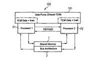
- traditional multiprocessor systems having processors P 1 , P 2use a shared memory 1 for interchanging data or instructions, which shared memory is connected via a bus architecture 2 both to the first processor P 1 and to the second processor P 2 .
- the interaction of the two processors P 1 , P 2can be controlled or synchronized by means of interrupts (commands for interrupting the current CPU cycle).
- a further possibility for interactive control of the memory accessconsists in providing semaphores, i.e.
- a software-controlled identificationdefining which of the processors is permitted to exercise a write access to the shared memory 1 .
- TCMtightly coupled memory
- the TCMis a DRAM, SRAM or flash memory that can essentially be directly connected to the processor core and can be accessed singly and solely by the processor P 1 , P 2 equipped with the respective TCM.
- Processors P 1 , P 2 that can be equipped with a TCMhave an input/output intended specifically for the TCM—a so-called TCM interface—and also a suitable address generating unit for generating the addresses for the TCM.
- processors P 1 , P 2 with a TCMhave an improved performance for dealing with computation- and data-intensive tasks.
- both processors P 1 , P 2are equipped with a TCM 3 .
- the real-time behaviour that can be achieved with this solutionstill remains unsatisfactory.
- SoCsystem-on-chip
- processor coresfor general tasks
- further componentssuch as, for example, an analogue front end, on-chip memory, input/output devices and other application-specific integrated circuits.
- the starting point for the development of an SoCis the definition of the processes or tasks that have to be dealt with by the SoC. Afterwards, it is necessary to find a suitable software/hardware partitioning. In this case, it is important to enable a high-performance task scheduling and a high-performance intertask communication in order to be able to comply with real-time requirements. At the same time, it is necessary to fulfil the customary requirements (small space requirement, low power consumption).
- the inventionis based on the object of specifying a multiprocessor system comprising processors embedded in a single chip, said multiprocessor system being well suited to computation- and data-intensive time-critical applications.
- the intentionis to be able to obtain a low power consumption and a small space requirement.
- the inventionaims to specify a method for communication between two processors with good performance in the case of computation- and data-intensive time-critical applications.
- the objective on which the invention is basedcan be achieved by a chip-integrated multiprocessor system comprising a first processor and a second processor each having an input/output set up for the connection of a tightly coupled semiconductor memory, and a shared tightly coupled integrated semiconductor memory, which can be accessed by both processors via their input/output.
- the processorseach may have an address generating unit which is assigned to the input/output and realises the address generation for accessing the shared tightly coupled semiconductor memory.
- the address generation for accessing the shared tightly coupled semiconductor memorymay be effected by means of a DMA address generating unit assigned to the input/output of the first and/or the second processor.
- a compression/decompression modulecan be arranged between the input/output of the first and/or the second processor and the shared tightly coupled semiconductor memory.
- An encryption/decryption modulecan be arranged between the input/output of the first and/or the second processor and the shared tightly coupled semiconductor memory.
- One or a plurality of buffer memoriescan be arranged between the input/output of the first and/or the second processor and the shared tightly coupled semiconductor memory.
- the shared tightly coupled semiconductor memorymay have one or a plurality of private memory areas which can be accessed in each case by only a single processor.
- the shared tightly coupled semiconductor memorycan be a two-port memory.
- the shared tightly coupled semiconductor memorycan be assigned a semiconductor memory expansion, in particular an SRAM memory, which can be accessed by the processors via the inputs/outputs.
- One processorcan be a digital signal processor and the other processor is a RISC microprocessor.
- the processorsfurthermore each may have further inputs/outputs via which they are connected via a bus architecture to a further shared memory.
- the objectcan furthermore be achieved by a chip-integrated multiprocessor system comprising a first processor and a second processor each having an input/output set up for the connection of a tightly coupled semiconductor memory, the shared tightly coupled integrated semiconductor memory coupled with said first and second processor, which can be accessed by both processors via their input/output, wherein the shared tightly coupled semiconductor memory has one or a plurality of private memory areas which can be accessed in each case by only a single processor, and a processing module arranged between the input/output of the first and/or the second processor and the shared tightly coupled semiconductor memory.
- the processorseach may have an address generating unit which is assigned to the input/output and realizes the address generation for accessing the shared tightly coupled semiconductor memory.
- the address generation for accessing the shared tightly coupled semiconductor memorycan be effected by means of a DMA address generating unit assigned to the input/output of the first and/or the second processor.
- the processing modulecan be a compression/decompression module or an encryption/decryption module.
- One or a plurality of buffer memoriescan be arranged between the input/output of the first and/or the second processor and the shared tightly coupled semiconductor memory.
- the shared tightly coupled semiconductor memorycan be a two-port memory.
- the shared tightly coupled semiconductor memorycan be assigned a semiconductor memory expansion, in particular an SRAM memory, which can be accessed by the processors via the inputs/outputs.
- One processorcan be a digital signal processor and the other processor can be a RISC microprocessor.
- the processorsfurthermore each may have further inputs/outputs via which they are connected via a bus architecture to a further shared memory.
- the objectcan also be achieved by a method for communication between two processors of a chip-integrated multiprocessor system which each have an input/output for accessing a shared tightly coupled semiconductor memory comprising the steps of:
- the methodmay also comprise the following steps:
- the methodmay also comprise the following steps:
- the methodmay also comprise the following steps:
- the chip-integrated multiprocessor systemcomprises a first processor and a second processor each having an input/output set up for connection of a tightly coupled semiconductor memory (TCM).
- TCMtightly coupled semiconductor memory
- the multiprocessor systemhas a shared tightly coupled integrated semiconductor memory which can be accessed by both processors via their input/output.
- the essential basic concept of the inventionthus consists in now providing, instead of the tightly coupled semiconductor memories that have been provided separately hitherto for each processor, a shared tightly coupled semiconductor memory for at least two processors and in utilizing it as a fast data and instruction connection between the processors.
- the shared tightly coupled semiconductor memory according to the inventionmakes it possible to save chip area on account of the shared utilization of memory area. Furthermore, a reduction of the power consumption is achieved in comparison with the prior art since the number of tightly coupled semiconductor memories is reduced in comparison with the prior art (where each processor has its own TCM).
- the address generation for accessing the shared tightly coupled semiconductor memory in the first and/or second processoris effected by means of a DMA address generating unit (DMA: Direct Memory Access).
- DMA address generating unitsare known in the prior art for their fast access to semiconductor memories. This measure enables an even faster interaction between the processors.
- a particularly preferred refinement of the inventionis characterized in that a compression/decompression module is arranged between the input/output of the first and/or the second processor and the shared tightly coupled semiconductor memory.
- This moduleembodied in dedicated hardware enables an efficient, i.e. memory space conserving utilization of the shared memory area.
- the modulealways carries out a compression/decompression of the data and/or instructions that are to be written or read out. In this way, the quantity of data and/or instructions to be stored in the tightly coupled semiconductor memory can be increased or the memory area can be reduced (for a given quantity).
- an encryption/decryption modulemay be provided between the input/output of the processors and the tightly coupled semiconductor memory. This increases the functionality of the solution according to the invention in the processing of security-relevant tasks (e.g. online banking).
- the shared tightly coupled semiconductor memoryhas one or a plurality of private memory areas which can be accessed in each case by only a single processor.
- the privacy of the individual tightly coupled semiconductor memories that is (necessarily) present in the prior artis thus also preserved for the shared tightly coupled semiconductor memory according to the invention (in the private memory areas).
- a further particular advantageous refinement of the multiprocessor system according to the inventionis characterized in that one or a plurality of buffer memories are arranged between the input/output of the first and/or the second processor and the shared tightly coupled semiconductor memory.
- the buffer memoriesmake it possible to compensate for transfer time fluctuations, latencies or generally temporal restrictions in the transfer of data and/or instructions between one processor and the other processor.
- the connection according to the invention for data/instructions between the two processorsbecomes more flexible with regard to the control of temporal sequences.
- a further advantageous measureis characterized in that the shared tightly coupled semiconductor memory is assigned an expansion memory, in particular an SRAM (static RAM), which can be accessed by the processors via the inputs/outputs.
- SRAMstatic RAM
- An advantageous embodiment variantis characterized in that one processor is a digital signal processor (DSP) and the other processor is a RISC microprocessor.
- DSPdigital signal processor
- the other processoris a RISC microprocessor.
- DSP-RISCdigital signal processor
- FIG. 1shows a schematic illustration of a multiprocessor system with a shared memory linked via a bus architecture and in each case a tightly coupled memory (TCM) for each processor;
- TCMtightly coupled memory
- FIG. 2shows a schematic illustration of the interaction of software and hardware in the implementation of an application for a general multiprocessor system (on the left) and for the specific example of a GSM modern (on the right);
- FIG. 3shows an illustration of the architecture of a known embedded processor with inputs/outputs for the connection of a tightly coupled memory
- FIG. 4shows a schematic illustration of an exemplary embodiment of a multiprocessor system according to the invention with a shared tightly coupled memory
- FIG. 5shows a schematic illustration of a first variant of the fast connection according to the invention between the processors.
- FIG. 6shows a schematic illustration of a second variant of the fast connection according to the invention between the processors.
- an application 10is subdivided into a plurality of tasks 11 .
- the application 10 and the tasks 11are constituent parts of the software (SW), i.e. defined by an application program.
- the tasks 11are divided between the two processors P 1 and P 2 of the hardware (HW).
- datae.g. received data of a mobile radio receiver
- control signals for the system controlare generated.
- some data or control signals 13are generated by both processors P 1 , P 2 while other data or control signals 14 are only calculated by one of the processors P 1 , P 2 .
- the tasksconsist on the one hand in a signal processing 15 of useful data which is carried out by a DSP (digital signal processor) 16 , and on the other hand in a processing of a protocol stack 17 for generating control signals, which is performed by a RISC microcontroller 18 .
- Data and/or instructions 19are generated, which can be interchanged between the DSP 16 and the RISC microcontroller 18 and also private data 20 , which are only accessed by in each case one of the two processors 16 , 18 .
- FIG. 3shows, in a simplified illustration using the example of the known RISC processor ARM926EJ-STM 50, the construction of a processor having inputs/outputs for the connection of a tightly coupled semiconductor memory (TCM).
- the central constituent part of the processor 50is the processor core 51 , in which the instruction set is implemented.
- the processor core 51is connected to a bus interface 55 for the data bus 2 via a data cache memory 52 and a writing buffer memory 54 . Instructions are forwarded from the processor core 51 via an instruction cache memory 53 and a buffer memory 56 to the bus interface 55 , or are received from the latter.
- the bus interface 55is connected to the processor core 51 via a filling buffer memory 57 and the data cache memory 52 .
- the processor 50furthermore has a central address generating unit MMU (Memory Management Unit) 58 and also a data TCM interface 59 and an instruction TCM interface 60 .
- Said TCM interfaces 59 and 60are specifically designed for the connection of a TCM 3 , which can be connected directly to the outputs/inputs of the TCM interfaces 59 , 60 .
- Instructions and data from the processor core 51are conducted to the data TCM interface 59 and to the instruction TCM interface 60 via a data TLB (Translation Lookaside Buffer) 61 —also called data associative memory—and, respectively, via an instruction TLB 62 —also called instruction associative memory.
- the associative memories 61 , 62may also be considered to be constituent parts of the MMU 58 , the task of which is to generate (virtual) addresses for the memory accesses.
- the processor 50also has a coprocessor interface 63 for connection of a coprocessor and an ETM (Embedded Trace Macrocell) interface 64 , which is used for program development. These two interfaces are not important for the present invention.
- connection between the process core 51 and the TCM interfaces 59 , 60has no writing and filling buffer memories and no cache memory. It is known to the person skilled in the art that the input/output of data and/or instructions can be carried out significantly faster via the TCM interfaces 59 , 60 than via the bus interface 55 .
- FIG. 4shows a schematic illustration of the multiprocessor system according to the invention. Components identical to those in FIG. 1 are designated by the same reference symbols.
- the essential difference from the microprocessor circuit shown in FIG. 1is that the processors P 1 and P 2 are assigned a shared tightly coupled semiconductor memory (shared TCM) 101 .
- the shared TCM 101has two logical inputs/outputs, in each case one for each processor P 1 , P 2 . Physically, however, the shared TCM 101 may be embodied as a two-port memory (dual ported RAM) or as a one-port memory (single ported RAM).
- the shared TCM 101forms the main constituent part of the fast connection that transfers data and instructions between the processors P 1 , P 2 , and is referred to hereinafter as “data pump” 100 .
- the multiprocessor systemis realised as an SoC solution, i.e. the processors P 1 , P 2 and also the data pump 100 are hardware modules embedded in the chip.
- a task 10consists for example in reading data from a lookup table and processing said data further in accordance with a predetermined application algorithm. Since the RISC microcontroller P 1 has a good performance for reading data from a table, this part of the task is performed by the RISC microcontroller P 1 . The data processing has to be carried out by the DSP P 2 in the next cycle. In order to achieve a fast communication of the data read out, the latter are forwarded from the RISC microcontroller 1 to the DSP P 2 via the shared TCM 101 . This requires write operations by the RISC microcontroller P 1 and read operations by the DSP P 2 .
- processors P 1 and P 2may be structurally unchanged with respect to the processors P 1 and P 2 each having a dedicated TCM 4 which are illustrated with respect to the prior art in FIG. 1 —that is to say may be realised e.g. by the known processor 50 illustrated in FIG. 3 .
- the address generating units MMU(embodied in hardware) in the respective processors P 1 and P 2 may remain unchanged.
- a DMAmay also be used as address generating unit MMU.
- the application softwarei.e. the application program 10
- a shared TCM 101is used as data pump between the processors P 1 , P 2 .
- the hardware independence—important for the reusability of the application program 10with regard to the solution according to the invention is thus maintained for the application program 10 .
- the approach according to the inventionis therefore markedly openOS-friendly (OS: Operating System).
- FIG. 5shows a first example 100 . 1 for the data pump 100 .
- the lattercomprises a TCM realised as a DRAM memory 101 , and also a plurality of optional buffer memories 102 .
- the DRAM memory 101has various memory areas: a shared memory area 103 that can be accessed (i.e. writing and reading access) by both processors P 1 and P 2 is mandatory.
- a private memory area 104may be provided for the processor P 1 (e.g. RISC microcontroller 18 ) and a private memory area 105 may be provided for the processor P 2 (e.g. DSP 16 ).
- the DRAM memory 101may furthermore contain a memory area 106 for semaphores (flags).
- the processor P 1accesses the tightly coupled DRAM memory 101 in a customary manner (i.e. via a data line (not illustrated), an address line (not illustrated) and a write/read changeover (not illustrated)). The same applies to the processor P 2 .
- a compression/decompression module 110may be arranged between the input/output 107 of the processor P 1 and the input/output 108 of the DRAM memory 101 .
- the module 110optionally carries out a compression or no compression of the data/instructions that are written to the DRAM memory 101 .
- the module 110automatically detects the status (compressed/not compressed) of the data/instructions to be read out and automatically carries out a decompression or no decompression in a manner dependent on the detected status.
- the input/output 107 of the processor P 1corresponds to the input/output of the data TCM interface 59 and the input/output of the instruction TCM interface 60 in FIG. 3 .
- the optional compression/decompression of data/instructions to be written/to be read by the module 110may be effected for example by the module 110 being informed under software control via a configuration register (not illustrated) of the module 110 , of the address area of the DRAM memory 101 in which compressed data are to be stored.
- the module 110is informed of the write or read address, and the module 110 checks whether or not the current address is present in the address area provided for storing compressed data. If this address area is addressed, the module 110 is activated; otherwise it remains inactive (or is deactivated).
- the processor P 2accesses the DRAM memory 101 in an analogous manner.
- the input/output of the processor P 2is designated by the reference symbol 109 . It likewise corresponds to the input/output of the data TCM interface 59 and the input/output of the instruction TCM interface 60 in FIG. 3 .
- the buffer memories 102are arranged in the signal path between the input/output 107 of the processor P 1 , and respectively the input/output 109 of the processor P 2 , and the input/output 108 of the DRAM memory 101 (the schematic illustration shown in FIG. 5 is intended merely to illustrate the (optional) presence of the buffer memories 102 ).
- the buffer memories 102enable the relaxation of time restrictions (occurrence of latencies) and the withholding of data packets e.g. in the case of data corruption.
- FIG. 6shows a second variant 100 . 2 of the data pump 100 according to the invention. Components identical to those in FIG. 5 are designated by the same reference symbols.
- the data pump 100 . 2 illustrated schematically in FIG. 6additionally comprises an expansion memory 120 , which is connected via a compression/decompression module 110 to the DRAM memory 101 , i.e. also to the input/output 107 of the processor P 1 and the input/output 109 of the processor P 2 .
- the functioning of the module 110has already been explained.
- the expansion memory 120may be embodied as an SRAM memory and constitutes a memory expansion for the data pump 100 . 2 .
- the module 110may also perform an encryption/decryption. This is likewise effected by means of a suitable dedicated hardware. Analogously to the address-area-dependent functioning of the module 110 in the case of data/instruction compression/data/instruction decompression, the encryption of a datum and/or of an instruction may also be automatically performed or omitted depending on the address allocated thereto.
- the tightly coupled semiconductor memory 101may be of arbitrary design, in principle, and may be realised for example as a DRAM, SRAM or flash memory.
- DRAM and SRAM memoriesenable particularly fast access times, while the flash memory affords the advantages of a non-volatile memory.
Landscapes
- Engineering & Computer Science (AREA)
- Computer Hardware Design (AREA)
- Theoretical Computer Science (AREA)
- Software Systems (AREA)
- Physics & Mathematics (AREA)
- General Engineering & Computer Science (AREA)
- General Physics & Mathematics (AREA)
- Multi Processors (AREA)
Abstract
Description
- writing of data and/or instructions to the shared semiconductor memory by the first processor; and
- reading of the data and/or instructions that have been written to the shared tightly coupled semiconductor memory by the first processor by the second processor.
- compression and/or encryption of the data and/or instructions that have been output by the first processor by means of a compression and/or encryption circuit;
- writing of the compressed and/or encrypted data and/or instructions to the shared tightly coupled semiconductor memory;
- decompression and/or decryption of the data/or instructions that are to be read from the shared tightly coupled semiconductor memory by the second processor by means of a decompression and/or decryption circuit; and
- reading of the decompressed and/or decrypted data and/or instructions by the second processor.
- temporary storage of data and/or instructions that are to be read from the shared tightly coupled semiconductor memory or are to be written to the shared tightly coupled semiconductor memory in at least one buffer memory.
- storage of data and/or instructions in an expansion memory assigned to the shared semiconductor memory by the first and/or the second processor.
Claims (26)
Applications Claiming Priority (3)
| Application Number | Priority Date | Filing Date | Title |
|---|---|---|---|
| DE102004009497 | 2004-02-27 | ||
| DE102004009497.7 | 2004-02-27 | ||
| DE102004009497ADE102004009497B3 (en) | 2004-02-27 | 2004-02-27 | Chip integrated multi-processor system e.g. for communications system, with 2 processors each having input/output coupled to common tightly-coupled memory |
Publications (2)
| Publication Number | Publication Date |
|---|---|
| US20050193081A1 US20050193081A1 (en) | 2005-09-01 |
| US7797496B2true US7797496B2 (en) | 2010-09-14 |
Family
ID=34625825
Family Applications (1)
| Application Number | Title | Priority Date | Filing Date |
|---|---|---|---|
| US10/941,119Expired - Fee RelatedUS7797496B2 (en) | 2004-02-27 | 2004-09-15 | Multiprocessor system having a shared tightly coupled memory and method for communication between a plurality of processors |
Country Status (3)
| Country | Link |
|---|---|
| US (1) | US7797496B2 (en) |
| CN (1) | CN1661585B (en) |
| DE (1) | DE102004009497B3 (en) |
Cited By (20)
| Publication number | Priority date | Publication date | Assignee | Title |
|---|---|---|---|---|
| US20100100683A1 (en)* | 2008-10-22 | 2010-04-22 | International Business Machines Corporation | Victim Cache Prefetching |
| US20100235577A1 (en)* | 2008-12-19 | 2010-09-16 | International Business Machines Corporation | Victim cache lateral castout targeting |
| US20100235651A1 (en)* | 2005-09-27 | 2010-09-16 | Sony Computer Entertainment, Inc. | Secure operation of processors |
| US20100235584A1 (en)* | 2009-03-11 | 2010-09-16 | International Business Machines Corporation | Lateral Castout (LCO) Of Victim Cache Line In Data-Invalid State |
| US20100257316A1 (en)* | 2009-04-07 | 2010-10-07 | International Business Machines Corporation | Virtual Barrier Synchronization Cache Castout Election |
| US20100257317A1 (en)* | 2009-04-07 | 2010-10-07 | International Business Machines Corporation | Virtual Barrier Synchronization Cache |
| US20110161589A1 (en)* | 2009-12-30 | 2011-06-30 | International Business Machines Corporation | Selective cache-to-cache lateral castouts |
| US20110289284A1 (en)* | 2010-05-19 | 2011-11-24 | Won-Seok Jung | Multi-processor device and inter-process communication method thereof |
| US8225045B2 (en) | 2008-12-16 | 2012-07-17 | International Business Machines Corporation | Lateral cache-to-cache cast-in |
| US8312220B2 (en) | 2009-04-09 | 2012-11-13 | International Business Machines Corporation | Mode-based castout destination selection |
| US8327073B2 (en) | 2009-04-09 | 2012-12-04 | International Business Machines Corporation | Empirically based dynamic control of acceptance of victim cache lateral castouts |
| US8347036B2 (en) | 2009-04-09 | 2013-01-01 | International Business Machines Corporation | Empirically based dynamic control of transmission of victim cache lateral castouts |
| US8347037B2 (en) | 2008-10-22 | 2013-01-01 | International Business Machines Corporation | Victim cache replacement |
| KR101275628B1 (en)* | 2011-09-29 | 2013-06-17 | 전자부품연구원 | Electronic chip using dual-port memory based TCM capable of variable area size |
| US8499124B2 (en) | 2008-12-16 | 2013-07-30 | International Business Machines Corporation | Handling castout cache lines in a victim cache |
| US20140143512A1 (en)* | 2012-11-16 | 2014-05-22 | International Business Machines Corporation | Accessing additional memory space with multiple processors |
| US9037838B1 (en)* | 2011-09-30 | 2015-05-19 | Emc Corporation | Multiprocessor messaging system |
| US9354812B1 (en) | 2015-02-12 | 2016-05-31 | Qualcomm Incorporated | Dynamic memory utilization in a system on a chip |
| US9760526B1 (en)* | 2011-09-30 | 2017-09-12 | EMC IP Holdings Company LLC | Multiprocessor messaging system |
| US9792244B2 (en) | 2015-02-13 | 2017-10-17 | Honeywell International Inc. | Multiple processor architecture with flexible external input/output interface |
Families Citing this family (33)
| Publication number | Priority date | Publication date | Assignee | Title |
|---|---|---|---|---|
| JP4831599B2 (en)* | 2005-06-28 | 2011-12-07 | ルネサスエレクトロニクス株式会社 | Processing equipment |
| KR100634566B1 (en)* | 2005-10-06 | 2006-10-16 | 엠텍비젼 주식회사 | User terminal performing shared memory control method and shared memory operation control |
| JP2007157150A (en)* | 2005-12-06 | 2007-06-21 | Samsung Electronics Co Ltd | Memory system and memory processing method including the same |
| KR101275752B1 (en) | 2005-12-06 | 2013-06-17 | 삼성전자주식회사 | Memory system and booting method thereof |
| KR100735612B1 (en)* | 2005-12-22 | 2007-07-04 | 삼성전자주식회사 | Multipath Accessible Semiconductor Memory Devices |
| DE102006003892B4 (en) | 2006-01-27 | 2018-03-08 | Saurer Germany Gmbh & Co. Kg | Method for storing operating state data of an electromotive drive of a textile machine comprising a plurality of individual motor driven work stations and a drive for carrying out such a method |
| US9158941B2 (en)* | 2006-03-16 | 2015-10-13 | Arm Limited | Managing access to content in a data processing apparatus |
| KR100748191B1 (en)* | 2006-04-06 | 2007-08-09 | 엠텍비젼 주식회사 | Device with shared memory and method for providing shared memory access status information |
| KR100782592B1 (en)* | 2006-08-10 | 2007-12-06 | 엠텍비젼 주식회사 | Device with shared memory and control method of shared memory |
| US8209527B2 (en) | 2006-10-26 | 2012-06-26 | Samsung Electronics Co., Ltd. | Memory system and memory management method including the same |
| US20080113525A1 (en)* | 2006-11-15 | 2008-05-15 | Sandisk Il Ltd. | Compact solid state drive and processor assembly |
| DE102007004280A1 (en)* | 2007-01-23 | 2008-07-24 | Siemens Ag | One-chip computer and tachograph |
| CN101911049B (en)* | 2007-12-12 | 2013-03-06 | Nxp股份有限公司 | Processing architecture |
| US8831680B2 (en)* | 2008-01-31 | 2014-09-09 | Qualcomm Incorporated | Flexible audio control in mobile computing device |
| US20100162258A1 (en)* | 2008-12-23 | 2010-06-24 | Sony Corporation | Electronic system with core compensation and method of operation thereof |
| KR101592974B1 (en)* | 2009-03-27 | 2016-02-12 | 삼성전자주식회사 | System device including a plurality of processors and method for declaring and using the same |
| US20110161620A1 (en)* | 2009-12-29 | 2011-06-30 | Advanced Micro Devices, Inc. | Systems and methods implementing shared page tables for sharing memory resources managed by a main operating system with accelerator devices |
| US8719543B2 (en)* | 2009-12-29 | 2014-05-06 | Advanced Micro Devices, Inc. | Systems and methods implementing non-shared page tables for sharing memory resources managed by a main operating system with accelerator devices |
| US8725931B1 (en) | 2010-03-26 | 2014-05-13 | Western Digital Technologies, Inc. | System and method for managing the execution of memory commands in a solid-state memory |
| US8782327B1 (en) | 2010-05-11 | 2014-07-15 | Western Digital Technologies, Inc. | System and method for managing execution of internal commands and host commands in a solid-state memory |
| US9026716B2 (en) | 2010-05-12 | 2015-05-05 | Western Digital Technologies, Inc. | System and method for managing garbage collection in solid-state memory |
| US8635412B1 (en) | 2010-09-09 | 2014-01-21 | Western Digital Technologies, Inc. | Inter-processor communication |
| US9021192B1 (en) | 2010-09-21 | 2015-04-28 | Western Digital Technologies, Inc. | System and method for enhancing processing of memory access requests |
| US9164886B1 (en) | 2010-09-21 | 2015-10-20 | Western Digital Technologies, Inc. | System and method for multistage processing in a memory storage subsystem |
| US8789065B2 (en) | 2012-06-08 | 2014-07-22 | Throughputer, Inc. | System and method for input data load adaptive parallel processing |
| CN102081591A (en)* | 2011-01-27 | 2011-06-01 | 中国第一汽车集团公司 | Application of dual-port memory in dual-CPU (Central Processing Unit) structure design |
| US9158670B1 (en) | 2011-06-30 | 2015-10-13 | Western Digital Technologies, Inc. | System and method for dynamically adjusting garbage collection policies in solid-state memory |
| US9448847B2 (en) | 2011-07-15 | 2016-09-20 | Throughputer, Inc. | Concurrent program execution optimization |
| US10099063B2 (en)* | 2012-07-02 | 2018-10-16 | Physio-Control, Inc. | Medical monitor-defibrillator with defibrillator and data operations processors |
| US20140331019A1 (en)* | 2013-05-06 | 2014-11-06 | Microsoft Corporation | Instruction set specific execution isolation |
| CN103400085A (en)* | 2013-07-30 | 2013-11-20 | 东莞宇龙通信科技有限公司 | Terminal |
| US9252131B2 (en)* | 2013-10-10 | 2016-02-02 | Globalfoundries Inc. | Chip stack cache extension with coherency |
| CN111221465B (en)* | 2018-11-23 | 2023-11-17 | 中兴通讯股份有限公司 | DSP processor, system and external memory space access method |
Citations (4)
| Publication number | Priority date | Publication date | Assignee | Title |
|---|---|---|---|---|
| US5386511A (en)* | 1991-04-22 | 1995-01-31 | International Business Machines Corporation | Multiprocessor system and data transmission apparatus thereof |
| US5522058A (en)* | 1992-08-11 | 1996-05-28 | Kabushiki Kaisha Toshiba | Distributed shared-memory multiprocessor system with reduced traffic on shared bus |
| US5627976A (en)* | 1991-08-23 | 1997-05-06 | Advanced Micro Devices, Inc. | Crossing transfers for maximizing the effective bandwidth in a dual-bus architecture |
| US6643763B1 (en)* | 2000-02-28 | 2003-11-04 | International Business Machines Corporation | Register pipe for multi-processing engine environment |
Family Cites Families (3)
| Publication number | Priority date | Publication date | Assignee | Title |
|---|---|---|---|---|
| KR100230454B1 (en)* | 1997-05-28 | 1999-11-15 | 윤종용 | Cache Memory Checking Method in Multiprocessing Systems |
| US6449699B2 (en)* | 1999-03-29 | 2002-09-10 | International Business Machines Corporation | Apparatus and method for partitioned memory protection in cache coherent symmetric multiprocessor systems |
| DE10128475A1 (en)* | 2001-06-12 | 2003-01-02 | Siemens Ag | Multiprocessor system with a shared memory associated with a priority processor allowing high frequency access to the memory thus ensuring high data processing rates |
- 2004
- 2004-02-27DEDE102004009497Apatent/DE102004009497B3/ennot_activeExpired - Fee Related
- 2004-09-15USUS10/941,119patent/US7797496B2/ennot_activeExpired - Fee Related
- 2004-09-20CNCN2004100798145Apatent/CN1661585B/ennot_activeExpired - Fee Related
Patent Citations (4)
| Publication number | Priority date | Publication date | Assignee | Title |
|---|---|---|---|---|
| US5386511A (en)* | 1991-04-22 | 1995-01-31 | International Business Machines Corporation | Multiprocessor system and data transmission apparatus thereof |
| US5627976A (en)* | 1991-08-23 | 1997-05-06 | Advanced Micro Devices, Inc. | Crossing transfers for maximizing the effective bandwidth in a dual-bus architecture |
| US5522058A (en)* | 1992-08-11 | 1996-05-28 | Kabushiki Kaisha Toshiba | Distributed shared-memory multiprocessor system with reduced traffic on shared bus |
| US6643763B1 (en)* | 2000-02-28 | 2003-11-04 | International Business Machines Corporation | Register pipe for multi-processing engine environment |
Non-Patent Citations (1)
| Title |
|---|
| Karl Guttag et al.; "A Single-Chip Multiprocessor for Multimedia: The MVP"; Texas Instruments, Houston, TX; computer Graphics and Applications; IEEE, vol. 12, Issue 6, pp. 53-64, Nov. 1992. |
Cited By (32)
| Publication number | Priority date | Publication date | Assignee | Title |
|---|---|---|---|---|
| US20100235651A1 (en)* | 2005-09-27 | 2010-09-16 | Sony Computer Entertainment, Inc. | Secure operation of processors |
| US8135867B2 (en) | 2005-09-27 | 2012-03-13 | Sony Computer Entertainment, Inc. | Secure operation of processors |
| US8209489B2 (en) | 2008-10-22 | 2012-06-26 | International Business Machines Corporation | Victim cache prefetching |
| US8347037B2 (en) | 2008-10-22 | 2013-01-01 | International Business Machines Corporation | Victim cache replacement |
| US20100100683A1 (en)* | 2008-10-22 | 2010-04-22 | International Business Machines Corporation | Victim Cache Prefetching |
| US8499124B2 (en) | 2008-12-16 | 2013-07-30 | International Business Machines Corporation | Handling castout cache lines in a victim cache |
| US8225045B2 (en) | 2008-12-16 | 2012-07-17 | International Business Machines Corporation | Lateral cache-to-cache cast-in |
| US20100235577A1 (en)* | 2008-12-19 | 2010-09-16 | International Business Machines Corporation | Victim cache lateral castout targeting |
| US8489819B2 (en) | 2008-12-19 | 2013-07-16 | International Business Machines Corporation | Victim cache lateral castout targeting |
| US20100235584A1 (en)* | 2009-03-11 | 2010-09-16 | International Business Machines Corporation | Lateral Castout (LCO) Of Victim Cache Line In Data-Invalid State |
| US8949540B2 (en) | 2009-03-11 | 2015-02-03 | International Business Machines Corporation | Lateral castout (LCO) of victim cache line in data-invalid state |
| US8095733B2 (en)* | 2009-04-07 | 2012-01-10 | International Business Machines Corporation | Virtual barrier synchronization cache castout election |
| US20100257317A1 (en)* | 2009-04-07 | 2010-10-07 | International Business Machines Corporation | Virtual Barrier Synchronization Cache |
| US20100257316A1 (en)* | 2009-04-07 | 2010-10-07 | International Business Machines Corporation | Virtual Barrier Synchronization Cache Castout Election |
| US8131935B2 (en)* | 2009-04-07 | 2012-03-06 | International Business Machines Corporation | Virtual barrier synchronization cache |
| US8312220B2 (en) | 2009-04-09 | 2012-11-13 | International Business Machines Corporation | Mode-based castout destination selection |
| US8327073B2 (en) | 2009-04-09 | 2012-12-04 | International Business Machines Corporation | Empirically based dynamic control of acceptance of victim cache lateral castouts |
| US8347036B2 (en) | 2009-04-09 | 2013-01-01 | International Business Machines Corporation | Empirically based dynamic control of transmission of victim cache lateral castouts |
| US9189403B2 (en) | 2009-12-30 | 2015-11-17 | International Business Machines Corporation | Selective cache-to-cache lateral castouts |
| US20110161589A1 (en)* | 2009-12-30 | 2011-06-30 | International Business Machines Corporation | Selective cache-to-cache lateral castouts |
| US20110289284A1 (en)* | 2010-05-19 | 2011-11-24 | Won-Seok Jung | Multi-processor device and inter-process communication method thereof |
| US9274860B2 (en)* | 2010-05-19 | 2016-03-01 | Samsung Electronics Co., Ltd. | Multi-processor device and inter-process communication method thereof |
| KR101275628B1 (en)* | 2011-09-29 | 2013-06-17 | 전자부품연구원 | Electronic chip using dual-port memory based TCM capable of variable area size |
| US9037838B1 (en)* | 2011-09-30 | 2015-05-19 | Emc Corporation | Multiprocessor messaging system |
| US9760526B1 (en)* | 2011-09-30 | 2017-09-12 | EMC IP Holdings Company LLC | Multiprocessor messaging system |
| US9760416B1 (en)* | 2011-09-30 | 2017-09-12 | EMC IP Holding Company LLC | Multiprocessor messaging system |
| US10698858B1 (en) | 2011-09-30 | 2020-06-30 | EMC IP Holding Company LLC | Multiprocessor messaging system |
| US9052840B2 (en) | 2012-11-16 | 2015-06-09 | International Business Machines Corporation | Accessing additional memory space with multiple processors |
| US9047057B2 (en)* | 2012-11-16 | 2015-06-02 | International Business Machines Corporation | Accessing additional memory space with multiple processors |
| US20140143512A1 (en)* | 2012-11-16 | 2014-05-22 | International Business Machines Corporation | Accessing additional memory space with multiple processors |
| US9354812B1 (en) | 2015-02-12 | 2016-05-31 | Qualcomm Incorporated | Dynamic memory utilization in a system on a chip |
| US9792244B2 (en) | 2015-02-13 | 2017-10-17 | Honeywell International Inc. | Multiple processor architecture with flexible external input/output interface |
Also Published As
| Publication number | Publication date |
|---|---|
| DE102004009497B3 (en) | 2005-06-30 |
| CN1661585B (en) | 2010-04-14 |
| US20050193081A1 (en) | 2005-09-01 |
| CN1661585A (en) | 2005-08-31 |
Similar Documents
| Publication | Publication Date | Title |
|---|---|---|
| US7797496B2 (en) | Multiprocessor system having a shared tightly coupled memory and method for communication between a plurality of processors | |
| US8850168B2 (en) | Processor apparatus and multithread processor apparatus | |
| US9459874B2 (en) | Instruction set architecture-based inter-sequencer communications with a heterogeneous resource | |
| US8661199B2 (en) | Efficient level two memory banking to improve performance for multiple source traffic and enable deeper pipelining of accesses by reducing bank stalls | |
| US20080270707A1 (en) | Data processor | |
| US7590774B2 (en) | Method and system for efficient context swapping | |
| US20040215893A1 (en) | Method for use of ternary cam to implement software programmable cache policies | |
| CA2395645A1 (en) | Dual-mode processor | |
| US9965395B2 (en) | Memory attribute sharing between differing cache levels of multilevel cache | |
| US11550731B2 (en) | Processing method and apparatus for translation lookaside buffer flush instruction | |
| US20140173203A1 (en) | Block Memory Engine | |
| EP1269328B1 (en) | System having a configurable cache/sram memory | |
| EP1446717A1 (en) | Method and apparatus for interfacing a processor to a coprocessor | |
| CN101178690B (en) | Low-power high-performance high-speed scratchpad | |
| US20020040450A1 (en) | Multiple trap avoidance mechanism | |
| JP2009296195A (en) | Encryption device using fpga with multiple cpu cores | |
| US20240045680A1 (en) | Coprocessor Register Renaming | |
| US9779044B2 (en) | Access extent monitoring for data transfer reduction | |
| US11080188B1 (en) | Method to ensure forward progress of a processor in the presence of persistent external cache/TLB maintenance requests | |
| CN109656477B (en) | STT-MRAM-based non-contact smart card SoC | |
| US20120159083A1 (en) | Systems and Methods for Processing Memory Transactions | |
| US20210406166A1 (en) | Extended memory architecture | |
| US20240296128A1 (en) | Efficient input/output memory management unit | |
| CN118012455A (en) | Configurable memory system and memory management method thereof | |
| TWI406136B (en) | Integration of a processor and a hardware silicon chip production of a single chip system |
Legal Events
| Date | Code | Title | Description |
|---|---|---|---|
| AS | Assignment | Owner name:INFINEON TECHNOLOGIES AG, GERMANY Free format text:ASSIGNMENT OF ASSIGNORS INTEREST;ASSIGNORS:GRUBER, HANS-GEORG;MIELENZ, CARSTEN;REEL/FRAME:015800/0886 Effective date:20040909 | |
| FEPP | Fee payment procedure | Free format text:PAYOR NUMBER ASSIGNED (ORIGINAL EVENT CODE: ASPN); ENTITY STATUS OF PATENT OWNER: LARGE ENTITY | |
| AS | Assignment | Owner name:INTEL MOBILE COMMUNICATIONS TECHNOLOGY GMBH, GERMA Free format text:ASSIGNMENT OF ASSIGNORS INTEREST;ASSIGNOR:INFINEON TECHNOLOGIES AG;REEL/FRAME:027548/0623 Effective date:20110131 | |
| AS | Assignment | Owner name:INTEL MOBILE COMMUNICATIONS GMBH, GERMANY Free format text:ASSIGNMENT OF ASSIGNORS INTEREST;ASSIGNOR:INTEL MOBILE COMMUNICATIONS TECHNOLOGY GMBH;REEL/FRAME:027556/0709 Effective date:20111031 | |
| FPAY | Fee payment | Year of fee payment:4 | |
| AS | Assignment | Owner name:INTEL DEUTSCHLAND GMBH, GERMANY Free format text:CHANGE OF NAME;ASSIGNOR:INTEL MOBILE COMMUNICATIONS GMBH;REEL/FRAME:037057/0061 Effective date:20150507 | |
| FEPP | Fee payment procedure | Free format text:MAINTENANCE FEE REMINDER MAILED (ORIGINAL EVENT CODE: REM.) | |
| LAPS | Lapse for failure to pay maintenance fees | Free format text:PATENT EXPIRED FOR FAILURE TO PAY MAINTENANCE FEES (ORIGINAL EVENT CODE: EXP.); ENTITY STATUS OF PATENT OWNER: LARGE ENTITY | |
| STCH | Information on status: patent discontinuation | Free format text:PATENT EXPIRED DUE TO NONPAYMENT OF MAINTENANCE FEES UNDER 37 CFR 1.362 | |
| FP | Lapsed due to failure to pay maintenance fee | Effective date:20180914 | |
| AS | Assignment | Owner name:INTEL CORPORATION, CALIFORNIA Free format text:ASSIGNMENT OF ASSIGNORS INTEREST;ASSIGNOR:INTEL DEUTSCHLAND GMBH;REEL/FRAME:061356/0001 Effective date:20220708 |