US7796965B2 - Method and circuit arrangement for field strength determination and integrated circuit - Google Patents
Method and circuit arrangement for field strength determination and integrated circuitDownload PDFInfo
- Publication number
- US7796965B2 US7796965B2US11/790,492US79049207AUS7796965B2US 7796965 B2US7796965 B2US 7796965B2US 79049207 AUS79049207 AUS 79049207AUS 7796965 B2US7796965 B2US 7796965B2
- Authority
- US
- United States
- Prior art keywords
- antenna
- circuit
- reference input
- field strength
- input value
- Prior art date
- Legal status (The legal status is an assumption and is not a legal conclusion. Google has not performed a legal analysis and makes no representation as to the accuracy of the status listed.)
- Active, expires
Links
- 238000000034methodMethods0.000titleclaimsabstractdescription30
- 230000000694effectsEffects0.000claimsabstractdescription5
- 239000003990capacitorSubstances0.000claimsdescription13
- 230000008878couplingEffects0.000claimsdescription13
- 238000010168coupling processMethods0.000claimsdescription13
- 238000005859coupling reactionMethods0.000claimsdescription13
- 238000011156evaluationMethods0.000claimsdescription6
- 230000004913activationEffects0.000claimsdescription3
- 238000005259measurementMethods0.000abstractdescription20
- 238000011161developmentMethods0.000description12
- 230000005540biological transmissionEffects0.000description10
- 238000004519manufacturing processMethods0.000description8
- 238000010586diagramMethods0.000description6
- 230000001419dependent effectEffects0.000description5
- 230000007774longtermEffects0.000description5
- 230000001939inductive effectEffects0.000description3
- 230000008569processEffects0.000description3
- 230000008859changeEffects0.000description2
- 238000012986modificationMethods0.000description2
- 230000004048modificationEffects0.000description2
- RYGMFSIKBFXOCR-UHFFFAOYSA-NCopperChemical compound[Cu]RYGMFSIKBFXOCR-UHFFFAOYSA-N0.000description1
- 229910052802copperInorganic materials0.000description1
- 239000010949copperSubstances0.000description1
- 125000004122cyclic groupChemical group0.000description1
- 230000003071parasitic effectEffects0.000description1
- 235000012239silicon dioxideNutrition0.000description1
- 230000009466transformationEffects0.000description1
- 230000001960triggered effectEffects0.000description1
- 238000004804windingMethods0.000description1
Images


Classifications
- H—ELECTRICITY
- H04—ELECTRIC COMMUNICATION TECHNIQUE
- H04B—TRANSMISSION
- H04B5/00—Near-field transmission systems, e.g. inductive or capacitive transmission systems
- H04B5/20—Near-field transmission systems, e.g. inductive or capacitive transmission systems characterised by the transmission technique; characterised by the transmission medium
- H04B5/24—Inductive coupling
- H04B5/26—Inductive coupling using coils
- B—PERFORMING OPERATIONS; TRANSPORTING
- B60—VEHICLES IN GENERAL
- B60R—VEHICLES, VEHICLE FITTINGS, OR VEHICLE PARTS, NOT OTHERWISE PROVIDED FOR
- B60R25/00—Fittings or systems for preventing or indicating unauthorised use or theft of vehicles
- B60R25/20—Means to switch the anti-theft system on or off
- B60R25/24—Means to switch the anti-theft system on or off using electronic identifiers containing a code not memorised by the user
- G—PHYSICS
- G01—MEASURING; TESTING
- G01R—MEASURING ELECTRIC VARIABLES; MEASURING MAGNETIC VARIABLES
- G01R29/00—Arrangements for measuring or indicating electric quantities not covered by groups G01R19/00 - G01R27/00
- G01R29/08—Measuring electromagnetic field characteristics
- G01R29/0864—Measuring electromagnetic field characteristics characterised by constructional or functional features
- G01R29/0871—Complete apparatus or systems; circuits, e.g. receivers or amplifiers
- H—ELECTRICITY
- H04—ELECTRIC COMMUNICATION TECHNIQUE
- H04B—TRANSMISSION
- H04B17/00—Monitoring; Testing
- H04B17/30—Monitoring; Testing of propagation channels
- H04B17/309—Measuring or estimating channel quality parameters
- H04B17/318—Received signal strength
- B—PERFORMING OPERATIONS; TRANSPORTING
- B60—VEHICLES IN GENERAL
- B60R—VEHICLES, VEHICLE FITTINGS, OR VEHICLE PARTS, NOT OTHERWISE PROVIDED FOR
- B60R2325/00—Indexing scheme relating to vehicle anti-theft devices
- B60R2325/10—Communication protocols, communication systems of vehicle anti-theft devices
- B60R2325/105—Radio frequency identification data [RFID]
Definitions
- the present inventionrelates to a method and a circuit arrangement for field strength determination and to an integrated circuit.
- an unlocking of the vehicleoccurs not with a mechanical key, but with an electronic key medium or an electronic key, for example, in the shape of a molded article, on which actuation elements are arranged.
- One or more integrated circuits, which realize the function of the electronic key medium or of the electronic key,are arranged on or in the key medium.
- a so-called base stationwhich communicates or exchanges data with the electronic key in a wireless manner, is placed in the motor vehicle as a counterpart to the electronic key.
- a useractuates an associated control element on the electronic key, as a result of which a data transmission is initiated between the electronic key or its integrated circuit and the base station. If the information transmitted between the base station and the electronic key corresponds to a stipulated protocol and has the expected content, the motor vehicle is unlocked with the aid of the base station.
- the base stationWhen the user operates a door handle of the motor vehicle, this is detected in the motor vehicle and reported to the base station.
- the base stationthereupon transmits a low-frequency carrier signal, for example, with a frequency of 125 kHz, to the electronic key medium.
- datamay also be transmitted to the electronic key medium by the low-frequency carrier signal.
- the key mediumTo receive the low-frequency carrier signal, the key medium has an antenna circuit with an antenna, for example, in the form of a coil, whereby the antenna circuit generates an output value, for example, a voltage, which is a function of the field strength and a function of characteristic parameters of the antenna circuit.
- an antenna circuitwith an antenna, for example, in the form of a coil, whereby the antenna circuit generates an output value, for example, a voltage, which is a function of the field strength and a function of characteristic parameters of the antenna circuit.
- German Patent Application DE 101 59 551 A1which corresponds to U.S. Pat. No. 6,922,553, and which is incorporated herein by reference.
- the output valueis used to determine the distance of the key medium from the base station or from one or more transmitting antennas.
- the position of the user or the key medium relative to the motor vehiclecan also be determined by so-called triangulation based on two determined distances from the particular antennas.
- devicesare known in which three antenna coils, each perpendicular to one another, are provided.
- the specific field strengths of the antenna coilsare vectorially superposed to calculate a resulting field strength.
- the distance between the antenna of the base station and the antenna of the key medium antenna circuithas been determined, it is then verified whether the determined distance lies within a permitted tolerance range. If this is the case, access to the motor vehicle is made possible by unlocking all or only certain locks. The unlocking of only certain locks can be made dependent on the position of the user relative to the motor vehicle.
- a distance or position determinationis performed in the key medium also based on a field strength measurement. If the position determination indicates that the user is in the required position for starting the engine, the engine is started.
- an output valueis generated by the antenna circuit, for example, an output voltage, which is a function of the field strength and a function of the characteristic parameters of the antenna circuit.
- the characteristic parameters of a particular antenna circuitrepresent the tolerances, production variations, and other specific properties of the components of the particular antenna circuit.
- each antenna circuithas its specific characteristic parameters, which can deviate considerably from one another in practice, different antenna circuit output voltages result in different antenna circuits at identical field strength. If, for example, an atypical table is provided in the particular key medium for distance calculation, in which an assignment of the output voltage to field strength is stored, this can lead to obvious errors in the distance calculation.
- a laborious calibration of the key media or the antenna circuitsusually takes place during a manufacturing process.
- a known reference field strengthcan be predefined from outside by a calibration station, which is used to generate a calibration value in the particular key medium.
- This methodis very laborious and takes into account only the parameter situation during the calibration process. A change in the characteristic parameters by long-term effects, temperature, and variable operating voltage cannot be detected by calibration during the manufacturing process; i.e., the distance measurement becomes accordingly poorer with such long-term effects.
- Another major problemis that the antenna circuit or its antenna is more greatly dampened depending on metallic objects in its environment, for example, a bunch of keys; as a result, its characteristic parameters are also substantially changed depending on the situation. These effects as well cannot be detected by calibration during the manufacturing process.
- the antenna circuitIn the method for determining the field strength of a carrier signal, at an antenna of an antenna circuit of an electronic key, the antenna circuit generates an output value, which is a function of the field strength and a function of characteristic parameters of the antenna circuit.
- the characteristic parameters of a particular antenna circuitrepresent the tolerances, production variations, and other specific properties of the components of the particular antenna circuit.
- the characteristic parametersare measured in the electronic key based on a reference input value generated within the electronic key itself; here, the antenna circuit during the measurement of the characteristic parameters is supplied with the reference input value—i.e., the reference input value serves as the input value of the antenna circuit during the measurement. Then, the characteristic parameters are saved.
- a first, field-induced output value of the antenna circuitis measured, the antenna circuit not being supplied with the reference input value during the measurement of the first output value.
- the field strengthis determined from the first output value and the characteristic parameters, an effect of the characteristic parameters on the field strength being compensated.
- the measurement of the characteristic parameterscan occur in a cyclic manner, as a result of which a continuous calibration of the antenna circuit can occur.
- the generation of the in-circuit reference input valueenables a calibration also without a laborious calibration process during manufacture. Because the calibration can take place continuously, a precise, long-term stable field strength measurement is possible, which also takes into account changed conditions in the surroundings, for example, metallic objects in the vicinity of the key medium or of the antenna circuit.
- the reference input valueis generated in the form of a reference input voltage and/or a reference input current with a predefined reference frequency and reference amplitude; a second output value is measured with an applied reference input value, and the characteristic parameters are determined from the second output value.
- the characteristic parameterscan be identical to the second output value or the second output value can be a measure for the characteristic parameters.
- the quotientis formed from the first, field-strength-determined output value and the second, reference input value-determined output value.
- the reference frequencyis set equal to a frequency of the carrier signal. In this way, the characteristic parameters are determined by the reference value at the appropriate operating frequency.
- the reference frequencyis derived from a frequency of the carrier signal. It can be assured in this way that the calibration takes place by means of the reference input value also at the actual operating frequency of the antenna circuit.
- a distance between the antenna and a transmitting antenna of a transmitter of the carrier signalis determined from the determined field strength.
- the field strengthis determined in addition at a second antenna and at a third antenna of the antenna circuit, whereby the antennas are each perpendicular to one another and a distance between the antennas and a transmitting antenna of a transmitter of the carrier signal is determined from the determined field strengths by superposition.
- Vectorial superposition of the field strengths calculated per antennamakes it possible to calculate the distance independent of an orientation of the antennas or of the key medium relative to the transmitting antenna.
- the antenna and a transmitting antenna of a transmitter of the carrier signalare mutually coupled.
- mutual or inductive couplingreference is made to the manual of Klaus Finkenzeller, RFID-Handbuch [RFID Manual], 3rd ed., HANSER, 2002; see in particular Chapter 3.2.1 “Inductive Coupling”, pages 42 to 45.
- a parallel resonant circuit or a series resonant circuitis formed by the antenna circuit.
- the frequency of the carrier signalis within a range of 50 KHz to 150 KHz or within a range of 5 MHz to 25 MHz.
- the circuit arrangement of the invention for determining the field strength of a carrier signalhas an antenna circuit with an antenna and an output terminal, at which an output value is applied in the form of an output voltage and/or an output current, which is a function of the field strength and a function of characteristic parameters of the antenna circuit.
- a reference input value generating unit for generating a reference input valueis provided in the form of a reference input voltage and/or a reference input current with a known reference frequency and reference amplitude, as well as an activatable switching unit, coupled to the antenna circuit and the reference input value generating unit, which supplies the antenna circuit with the reference input value as a function of the activation state or decouples the antenna circuit from the reference input value.
- the reference input value generating unitis an oscillator.
- the oscillatormay comprise, for example, a PLL, quartzes, voltage-controlled oscillators, etc.
- said arrangementcomprises an evaluation unit, which is designed in such a way that it evaluates an output value when a reference input value is not applied and an output value when a reference input value is applied for determining the field strength.
- the evaluation unitmay be, for example, a microcontroller with a low power requirement.
- the antenna circuithas an antenna coil and a capacitor, which together form a parallel resonant circuit.
- the switching unithas a first switch, which is looped between a terminal of the capacitor and a reference potential, particularly ground, and a second switch, which is looped between the terminal of the capacitor and a terminal of the reference input value generating unit, at which the reference input value is applied.
- the switchesare activated in such a way that the reference input value serves as an input value of the antenna circuit, when the characteristic parameters are determined, and that the antenna circuit is decoupled from the reference input value or the reference input value generating unit, when the field strength is measured.
- the antenna circuitis designed for mutual coupling to a transmitting antenna of a transmitter of the carrier signal.
- the integrated circuit of the invention for a key medium of a passive entry and/or a passive go systemis designed for coupling to a circuit arrangement.
- FIG. 1illustrates a block diagram of a passive entry/passive go system for automatic, distance-dependent unlocking and/or locking and for keyless starting of a motor vehicle;
- FIG. 2illustrates a detailed block diagram of a key medium and a base station of FIG. 1 ;
- FIG. 3illustrates a detailed block diagram of an antenna circuit of an LF transmitter/receiver of FIG. 2 .
- FIG. 1shows a block diagram of a passive entry/passive go (PEG) system for automatic, distance-dependent unlocking and/or locking and for keyless starting of a motor vehicle 100 .
- PEGpassive entry/passive go
- the PEG systemcomprises a base station 110 , which is placed in motor vehicle 100 , and at least one card-shaped, electronic key medium 200 assigned to base station 110 .
- a user (not shown) of key medium 200operates a door handle 120 of motor vehicle 100 , this is detected in motor vehicle 100 and reported to base station 110 , for example, via a motor vehicle bus system (not shown).
- Base station 110thereupon transmits a low-frequency (LF) carrier signal with a frequency of 125 kHz over an LF antenna of base station 110 in the form of a coil 114 to electronic key medium 200 .
- Key medium 200after receiving the LF carrier signal and a distance determination using the LF carrier signal field strength, calculated in the key medium 200 , transmits a signal with unlocking information in a UHF frequency range to base station 110 , when the determined or calculated distance is within a permissible range.
- LFlow-frequency
- the UHF signalis received by a UHF antenna 115 of base station 110 , and when the information transmitted from key medium 200 to base station 110 conforms with the protocol, motor vehicle 100 is unlocked, and the user can sit, for example, on a driver's seat (not shown) of motor vehicle 100 .
- a start buttonTo start motor vehicle 100 , the user presses a start button, whereupon the low-frequency LF carrier signal is again transmitted to key medium 200 . After a repeated distance or position calculation in key medium 200 , during which it is verified whether the user is sitting in a driver's seat (not shown), a start release is transmitted by key medium 200 , again via the UHF channel, to base station 110 .
- the UHF transmissionis based on a so-called far-field coupling and the LF transmission on an inductive or mutual coupling in the near field. If more than one antenna 114 is placed at different positions in motor vehicle 100 , apart from a distance measurement, a position measurement relative to motor vehicle 100 can also be made by determining the respective antenna field strength, calculation of the distance to the respective antenna from the field strength, and subsequent triangulation.
- FIG. 2shows a detailed block diagram of key medium 200 and base station 110 of FIG. 1 .
- Base station 110comprises an LF transmitter/receiver 111 and LF antenna 114 in the form of a coil, connected to LF transmitter/receiver 111 , a UHF transmitter/receiver 113 , a UHF antenna 115 , connected to UHF transmitter/receiver 113 , and a microprocessor 112 , which is coupled to LF transmitter/receiver 111 and UHF transmitter/receiver 113 and exchanges data, to be transmitted and received bidirectionally, with said transmitter/receiver.
- Key medium 200comprises an LF transmitter/receiver 201 for a so-called 3D reception, to which antennas 202 , 203 , and 204 are connected in the form of coils.
- the antenna coils or symmetry axes in the winding direction of antenna coils 202 , 203 , and 204are each perpendicular to one another.
- the field strengths calculated per antennacan be interpreted as components of a three-dimensional field strength vector, whose contribution has a value dependent on the distance of key medium 200 from transmitting antenna 114 of base station 110 , but the value is independent of an orientation of key medium 200 relative to transmitting antenna 114 .
- key medium 200For UHF transmission, key medium 200 has a UHF transmitter/receiver 207 and a UHF antenna 208 connected to UHF transmitter/receiver 207 .
- key medium 200has a microprocessor 205 , which is coupled to LF transmitter/receiver 201 and UHF transmitter/receiver 207 and exchanges data, to be transmitted and received bidirectionally, with said transmitters/receivers, and a battery or an accumulator 206 for supplying power.
- LF transmitter/receiver 201in addition outputs a field strength signal, associated with each of antennas 202 , 203 , and 204 , to microprocessor 205 .
- an LF data transmissionoccurs unidirectionally from base station 110 to key medium 200 , whereby in this case, unit 111 is only a transmitter and unit 201 only a receiver. Accordingly, the UHF data transmission can occur unidirectionally from key medium 200 to base station 110 , whereby in this case, unit 207 is only a transmitter and unit 113 only a receiver. In the shown exemplary embodiment, both the LF data transmission and the UHF data transmission occur bidirectionally.
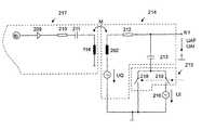
- FIG. 3shows a detailed block diagram of an antenna circuit 214 of LF transmitter/receiver 201 of FIG. 2 . For reasons of clarity, only the antenna circuit which is assigned to antenna 202 is shown in FIG. 3 . Antennas 203 and 204 are assigned corresponding antenna circuits (not shown).
- Antenna circuit 214comprises antenna or antenna coil 202 , a resistor 212 , which represents a parasitic copper resistor of antenna coil 202 , and a capacitor 213 .
- Antenna coil 202 and capacitor 213form a parallel resonant circuit.
- An output valuewhich during normal operation is a function of the field strength of the LF carrier signal and a function of characteristic parameters of antenna circuit 214 , is applied at the output terminal N 1 in the form of an output voltage UAF or UAI.
- the output voltage UAF or UAIis used as an analog input value for an A/D converter (not shown) of microprocessor 205 and is processed further digitalized in said microprocessor.
- a signal with a frequency f 0is provided via a driver stage 209 .
- the signalis supplied to a series resonant circuit with transmitting antenna coil 114 , a resistor 210 , and a capacitor 211 .
- a voltage UQis induced in antenna coil 202 by a magnetic carrier field generated in transmitting antenna coil 114 .
- the following formulasdescribe in mathematic terms the coupling between antenna coils 114 and 202 .
- UQdesignates a voltage induced in coil 202 ;
- ⁇ 0is the angular frequency assigned to the transmission frequency f 0 ,
- kis a coupling factor,
- L1is an inductance of antenna coil 114 ,
- L2is an inductance of antenna coil 202 , and
- i 1is a current through transmitting antenna coil 114 .
- the voltage UQ induced in antenna coil 202generates the following output voltage UAF:
- Equation (2)shows directly that the output voltage UAF, produced by the field of the carrier signal, is determined by the value R2 of resistor 212 , the inductance L2 of receiving coil 202 , and the capacitance C2 of capacitor 213 . These values therefore form the characteristic parameters of antenna circuit 214 .
- a switching unit 215activated by microprocessor 205 , with a first switch 218 and a second switch 219 , is activated in such a way that switch 218 is opened and switch 219 is closed.
- antenna circuit 214is supplied with the reference input value UI as a simulated input voltage.
- Switching unit 215is part of LF transmitter/receiver 201 of FIG. 2 .
- An output voltage UAI arising at output terminal N 1 of antenna circuit 214can be calculated using the following equation:
- UAIUI ( ⁇ 0 * R2 * C2 ) 2 + ( 1 - ⁇ 0 2 * L2 * C2 ) 2 ( 3 )
- Equation (4)is solved for UQ, we obtain:
- a distance x of the transmitting antenna or transmitting coil 114 of receiving antenna or receiving coil 202can be calculated from the calculated voltage UQ using the following Equation (6):
- Equation (6)applies to air coils as transmitting antenna 114 and receiving antenna 202 . If no air coils are used, Equation (6) can be modified accordingly. For this purpose, the coupling factor dependent on the distance x (by transformation of Equation (1))
- Equation (6)is to be replaced by a coupling factor valid for an employed coil type.
- a coupling factor valid for an employed coil typefor this purpose, reference is again made, for example, to Finkenzeller, see particularly page 108 , or the data book: ATMEL, Data Book 2001, ICs for wireless control systems, pages 326ff.
- the field strength or the distanceis determined as follows:
- switching unit 215is activated by microprocessor 205 such that antenna circuit 214 is supplied with the reference input value UI.
- the reference input value UIcan be permanently active or activated solely for the measuring process. Here, it should be known or made certain that the carrier signal is not active.
- switching unit 215After storage of output voltage UAI generated by turning on reference voltage source 216 , switching unit 215 is activated by microprocessor 205 in such a way that antenna circuit 214 is decoupled from the reference input value UI. The now arising output voltage UAF is produced by the field of the carrier signal at antenna coil 202 .
- the actual field strengthi.e., the field strength at which an effect of the characteristic parameters is compensated, is calculated by forming the ratio of UAF and UAI and multiplying by the known voltage UI.
- the specific field strengths, determined as described above, of antennas 202 , 203 , and 204are superposed for calculating a total field strength, which is independent of the orientation.
- the distanceis finally calculated using Equation (6) from the total field strength calculated by conventional vector calculus.
- the measurement of the voltage UAIcan be measured cyclically or triggered by certain events, as a result of which a change in the characteristic parameters of the antenna circuit, for example, due to a temperature drift, is taken into account.
- switch 218must remain closed in switching unit 215 during the measurement of the characteristic parameters and a reference current source supplies its current to a connection node between resistor 212 and capacitor 213 .
- the shown embodimentsenable a precise, long-term stable field strength or distance measurement, without a laborious calibration being necessary during a manufacturing process.
Landscapes
- Engineering & Computer Science (AREA)
- Physics & Mathematics (AREA)
- Electromagnetism (AREA)
- Computer Networks & Wireless Communication (AREA)
- Signal Processing (AREA)
- Mechanical Engineering (AREA)
- General Physics & Mathematics (AREA)
- Quality & Reliability (AREA)
- Lock And Its Accessories (AREA)
- Near-Field Transmission Systems (AREA)
- Testing Electric Properties And Detecting Electric Faults (AREA)
Abstract
Description
UQ=ω0*k√{square root over (L1*L2)}*i1 (1)
Claims (18)
Priority Applications (1)
| Application Number | Priority Date | Filing Date | Title |
|---|---|---|---|
| US11/790,492US7796965B2 (en) | 2006-04-25 | 2007-04-25 | Method and circuit arrangement for field strength determination and integrated circuit |
Applications Claiming Priority (5)
| Application Number | Priority Date | Filing Date | Title |
|---|---|---|---|
| DEDE102006020423.9 | 2006-04-25 | ||
| DE102006020423ADE102006020423B3 (en) | 2006-04-25 | 2006-04-25 | Method and circuit arrangement for field strength determination |
| DE102006020423 | 2006-04-25 | ||
| US80140106P | 2006-05-19 | 2006-05-19 | |
| US11/790,492US7796965B2 (en) | 2006-04-25 | 2007-04-25 | Method and circuit arrangement for field strength determination and integrated circuit |
Publications (2)
| Publication Number | Publication Date |
|---|---|
| US20070257770A1 US20070257770A1 (en) | 2007-11-08 |
| US7796965B2true US7796965B2 (en) | 2010-09-14 |
Family
ID=38537065
Family Applications (1)
| Application Number | Title | Priority Date | Filing Date |
|---|---|---|---|
| US11/790,492Active2029-02-04US7796965B2 (en) | 2006-04-25 | 2007-04-25 | Method and circuit arrangement for field strength determination and integrated circuit |
Country Status (5)
| Country | Link |
|---|---|
| US (1) | US7796965B2 (en) |
| EP (1) | EP2010926A2 (en) |
| CN (1) | CN101473234A (en) |
| DE (1) | DE102006020423B3 (en) |
| WO (1) | WO2007121995A2 (en) |
Cited By (8)
| Publication number | Priority date | Publication date | Assignee | Title |
|---|---|---|---|---|
| US20100077094A1 (en)* | 2008-09-24 | 2010-03-25 | Embarq Holdings Company, Llc | System and method for updating vehicle media content |
| US20100075655A1 (en)* | 2008-09-24 | 2010-03-25 | Embarq Holdings Company,Llc | System and method for controlling vehicle systems from a cell phone |
| US20100075656A1 (en)* | 2008-09-24 | 2010-03-25 | Embarq Holdings Company, Llc | System and method for key free access to a vehicle |
| US20100321154A1 (en)* | 2009-06-18 | 2010-12-23 | Lear Corporation | Method and system of determining and preventing relay attack for passive entry system |
| US20110241840A1 (en)* | 2008-12-03 | 2011-10-06 | Nationz Technologies Inc. | Method and device for improving communication distance accuracy of a transaction system via temperature compensation |
| FR2978784A1 (en)* | 2011-08-05 | 2013-02-08 | Continental Automotive France | METHOD AND DEVICE FOR RELEASING, BY MEANS OF AN RFID READER, A METHOD OF ACTUATING MEANS FOR CONDEMNATION / DE-CONDEMNATION OF ACCESS DOORS OF A MOTOR VEHICLE |
| US8718478B2 (en) | 2007-10-12 | 2014-05-06 | Corning Cable Systems Llc | Hybrid wireless/wired RoF transponder and hybrid RoF communication system using same |
| US8867919B2 (en) | 2007-07-24 | 2014-10-21 | Corning Cable Systems Llc | Multi-port accumulator for radio-over-fiber (RoF) wireless picocellular systems |
Families Citing this family (5)
| Publication number | Priority date | Publication date | Assignee | Title |
|---|---|---|---|---|
| CN102044101B (en)* | 2010-11-30 | 2012-07-25 | 深圳市航盛电子股份有限公司 | Smart card positioning method for automobile wireless access control system |
| FR2987196B1 (en)* | 2012-02-17 | 2014-04-04 | Continental Automotive France | METHOD AND DEVICE FOR ANTENNA DIAGNOSIS |
| DE102013110819A1 (en)* | 2013-09-30 | 2015-04-02 | Huf Hülsbeck & Fürst Gmbh & Co. Kg | Electronic component for an ID transmitter of a vehicle |
| US20160059827A1 (en)* | 2014-08-27 | 2016-03-03 | Lear Corporation | Optimizing uwb satellite antenna in-vehicle positioning |
| US11047832B2 (en)* | 2019-08-29 | 2021-06-29 | Endra Life Sciences Inc. | Method and system for determining at least one parameter of interest of a material |
Citations (19)
| Publication number | Priority date | Publication date | Assignee | Title |
|---|---|---|---|---|
| US2295629A (en) | 1940-10-31 | 1942-09-15 | Rca Corp | Frequency control system |
| US2489908A (en) | 1946-10-29 | 1949-11-29 | Gen Electric | Calibrator for field intensity recorders |
| US4272719A (en)* | 1978-02-27 | 1981-06-09 | Takeda Riken Kogyo Kabushikikaisha | Electric field intensity measuring apparatus |
| US4314251A (en)* | 1979-07-30 | 1982-02-02 | The Austin Company | Remote object position and orientation locater |
| US4619002A (en)* | 1984-07-02 | 1986-10-21 | Motorola, Inc. | Self-calibrating signal strength detector |
| US4642786A (en)* | 1984-05-25 | 1987-02-10 | Position Orientation Systems, Ltd. | Method and apparatus for position and orientation measurement using a magnetic field and retransmission |
| US5193210A (en)* | 1991-07-29 | 1993-03-09 | Abc Auto Alarms, Inc. | Low power RF receiver |
| GB2307050A (en) | 1995-11-04 | 1997-05-14 | Motorola Ltd | Method and apparatus for measuring antenna performance |
| US5723911A (en)* | 1994-03-17 | 1998-03-03 | Siemens Aktiengesellschaft | Keyless access control device |
| US6150811A (en)* | 1995-10-18 | 2000-11-21 | Mannesmann Vdo Ag | Magnetic field sensor for stable magnetic field measurement over a wide temperature range |
| US6259918B1 (en)* | 1999-02-26 | 2001-07-10 | Telefonaktiebolaget Lm (Publ) | Preservation of cell borders at hand-off within a smart antenna cellular system |
| EP1136955A2 (en) | 2000-03-20 | 2001-09-26 | Philips Corporate Intellectual Property GmbH | Arrangement for a security access system |
| US6300882B1 (en)* | 2000-04-18 | 2001-10-09 | Mitsubishi Denki Kabushiki Kaisha | Vehicle-onboard DSRC apparatus |
| DE10159551A1 (en) | 2001-12-05 | 2003-06-12 | Atmel Germany Gmbh | Method for obtaining field strength information |
| US6809638B2 (en)* | 2002-08-20 | 2004-10-26 | Trw Inc. | Apparatus with receiver having selectable threshold time constant |
| US7120564B2 (en)* | 2003-04-03 | 2006-10-10 | Metrotech Corporation | Buried line locator with integral position sensing |
| US20070139171A1 (en) | 2005-12-20 | 2007-06-21 | Harald Fischer | Method for transmitting information and signal transmission system, particularly for access control |
| US20070257771A1 (en)* | 2006-04-25 | 2007-11-08 | Daniel Moser | Passive entry and/or passive go system and associated operating method |
| US7602274B2 (en)* | 2004-04-23 | 2009-10-13 | Microchip Technology Incorporated | Dynamic configuration of a radio frequency transponder |
- 2006
- 2006-04-25DEDE102006020423Apatent/DE102006020423B3/enactiveActive
- 2007
- 2007-04-25EPEP07724550Apatent/EP2010926A2/ennot_activeWithdrawn
- 2007-04-25WOPCT/EP2007/003620patent/WO2007121995A2/enactiveApplication Filing
- 2007-04-25CNCN200780022832.1Apatent/CN101473234A/enactivePending
- 2007-04-25USUS11/790,492patent/US7796965B2/enactiveActive
Patent Citations (23)
| Publication number | Priority date | Publication date | Assignee | Title |
|---|---|---|---|---|
| US2295629A (en) | 1940-10-31 | 1942-09-15 | Rca Corp | Frequency control system |
| US2489908A (en) | 1946-10-29 | 1949-11-29 | Gen Electric | Calibrator for field intensity recorders |
| US4272719A (en)* | 1978-02-27 | 1981-06-09 | Takeda Riken Kogyo Kabushikikaisha | Electric field intensity measuring apparatus |
| US4314251A (en)* | 1979-07-30 | 1982-02-02 | The Austin Company | Remote object position and orientation locater |
| US4642786A (en)* | 1984-05-25 | 1987-02-10 | Position Orientation Systems, Ltd. | Method and apparatus for position and orientation measurement using a magnetic field and retransmission |
| US4619002A (en)* | 1984-07-02 | 1986-10-21 | Motorola, Inc. | Self-calibrating signal strength detector |
| US5193210A (en)* | 1991-07-29 | 1993-03-09 | Abc Auto Alarms, Inc. | Low power RF receiver |
| US5723911A (en)* | 1994-03-17 | 1998-03-03 | Siemens Aktiengesellschaft | Keyless access control device |
| US6150811A (en)* | 1995-10-18 | 2000-11-21 | Mannesmann Vdo Ag | Magnetic field sensor for stable magnetic field measurement over a wide temperature range |
| GB2307050A (en) | 1995-11-04 | 1997-05-14 | Motorola Ltd | Method and apparatus for measuring antenna performance |
| US6259918B1 (en)* | 1999-02-26 | 2001-07-10 | Telefonaktiebolaget Lm (Publ) | Preservation of cell borders at hand-off within a smart antenna cellular system |
| EP1136955A2 (en) | 2000-03-20 | 2001-09-26 | Philips Corporate Intellectual Property GmbH | Arrangement for a security access system |
| US20010033222A1 (en)* | 2000-03-20 | 2001-10-25 | Juergen Nowottnick | Passive keyless entry system |
| US6747545B2 (en) | 2000-03-20 | 2004-06-08 | Koninklijke Philips Electronics N.V. | Passive keyless entry system |
| US6300882B1 (en)* | 2000-04-18 | 2001-10-09 | Mitsubishi Denki Kabushiki Kaisha | Vehicle-onboard DSRC apparatus |
| DE10159551A1 (en) | 2001-12-05 | 2003-06-12 | Atmel Germany Gmbh | Method for obtaining field strength information |
| US6922553B2 (en) | 2001-12-05 | 2005-07-26 | Atmel Germany Gmbh | Method and circuit for obtaining field strength information |
| US6809638B2 (en)* | 2002-08-20 | 2004-10-26 | Trw Inc. | Apparatus with receiver having selectable threshold time constant |
| US7120564B2 (en)* | 2003-04-03 | 2006-10-10 | Metrotech Corporation | Buried line locator with integral position sensing |
| US7602274B2 (en)* | 2004-04-23 | 2009-10-13 | Microchip Technology Incorporated | Dynamic configuration of a radio frequency transponder |
| US20070139171A1 (en) | 2005-12-20 | 2007-06-21 | Harald Fischer | Method for transmitting information and signal transmission system, particularly for access control |
| EP1808818A1 (en) | 2005-12-20 | 2007-07-18 | ATMEL Germany GmbH | Method for transmitting information and signal transmission system, in particular for access control |
| US20070257771A1 (en)* | 2006-04-25 | 2007-11-08 | Daniel Moser | Passive entry and/or passive go system and associated operating method |
Non-Patent Citations (4)
| Title |
|---|
| Atmel, "Wireless Control Systems", Data Book 2001, ICs, p. 326. |
| Klaus Finkenzeller; "Inductive Coupling", RFID-Manual, 3rd edition, Hanser 2002, pp: 42-45. |
| Klaus Finkenzeller; "Measurement of system parameters" RFID-Manual, 3rd edition, Hanser 2002, pp: 103-104. |
| Klaus Finkenzeller; RFID-Manual, 3rd edition, Hanser 2002, pp: 72-73, and 77. |
Cited By (16)
| Publication number | Priority date | Publication date | Assignee | Title |
|---|---|---|---|---|
| US8867919B2 (en) | 2007-07-24 | 2014-10-21 | Corning Cable Systems Llc | Multi-port accumulator for radio-over-fiber (RoF) wireless picocellular systems |
| US8718478B2 (en) | 2007-10-12 | 2014-05-06 | Corning Cable Systems Llc | Hybrid wireless/wired RoF transponder and hybrid RoF communication system using same |
| US8538408B2 (en) | 2008-09-24 | 2013-09-17 | Centurylink Intellectual Property Llc | System and method for controlling vehicle systems from a cell phone |
| US20100075655A1 (en)* | 2008-09-24 | 2010-03-25 | Embarq Holdings Company,Llc | System and method for controlling vehicle systems from a cell phone |
| US20100075656A1 (en)* | 2008-09-24 | 2010-03-25 | Embarq Holdings Company, Llc | System and method for key free access to a vehicle |
| US20100077094A1 (en)* | 2008-09-24 | 2010-03-25 | Embarq Holdings Company, Llc | System and method for updating vehicle media content |
| US8126450B2 (en)* | 2008-09-24 | 2012-02-28 | Embarq Holdings Company Llc | System and method for key free access to a vehicle |
| US8224313B2 (en)* | 2008-09-24 | 2012-07-17 | Centurylink Intellectual Property Llc | System and method for controlling vehicle systems from a cell phone |
| US8819182B2 (en) | 2008-09-24 | 2014-08-26 | Centurylink Intellectual Property Llc | System and method for updating vehicle media content |
| US20110241840A1 (en)* | 2008-12-03 | 2011-10-06 | Nationz Technologies Inc. | Method and device for improving communication distance accuracy of a transaction system via temperature compensation |
| US8682271B2 (en)* | 2008-12-03 | 2014-03-25 | Nationz Technologies, Inc. | Method and device for improving communication distance accuracy of a transaction system via temperature compensation |
| US8587403B2 (en)* | 2009-06-18 | 2013-11-19 | Lear Corporation | Method and system of determining and preventing relay attack for passive entry system |
| US20100321154A1 (en)* | 2009-06-18 | 2010-12-23 | Lear Corporation | Method and system of determining and preventing relay attack for passive entry system |
| WO2013020644A1 (en)* | 2011-08-05 | 2013-02-14 | Continental Automotive France | Method and device for triggering, using an rfid reader, a procedure for actuating a means for locking/unlocking the access doors of an automobile |
| FR2978784A1 (en)* | 2011-08-05 | 2013-02-08 | Continental Automotive France | METHOD AND DEVICE FOR RELEASING, BY MEANS OF AN RFID READER, A METHOD OF ACTUATING MEANS FOR CONDEMNATION / DE-CONDEMNATION OF ACCESS DOORS OF A MOTOR VEHICLE |
| US9530261B2 (en) | 2011-08-05 | 2016-12-27 | Continental Automotive France | Method and device for triggering, using an RFID reader, a procedure for actuating a means for locking/unlocking the access doors of a motor vehicle |
Also Published As
| Publication number | Publication date |
|---|---|
| DE102006020423B3 (en) | 2007-10-25 |
| WO2007121995A2 (en) | 2007-11-01 |
| US20070257770A1 (en) | 2007-11-08 |
| EP2010926A2 (en) | 2009-01-07 |
| WO2007121995A3 (en) | 2008-01-31 |
| CN101473234A (en) | 2009-07-01 |
Similar Documents
| Publication | Publication Date | Title |
|---|---|---|
| US7796965B2 (en) | Method and circuit arrangement for field strength determination and integrated circuit | |
| US8525672B2 (en) | Passive entry and/or passive go system and associated operating method | |
| US7978049B2 (en) | Time-of-flight ranging systems using coarse and fine measurements | |
| US8299891B2 (en) | Antitheft system for vehicle | |
| US7061369B2 (en) | Method for measuring distance between two objects and method for controlling access to an object or the use thereof, in particular access control and driving authorization for a motor vehicle | |
| KR100477234B1 (en) | Car security system | |
| JP5615326B2 (en) | Position determination system for portable device, position determination method for portable device, position determination device for portable device | |
| CN105093171A (en) | System and method of locating a key | |
| US20170327083A1 (en) | Method and system for secure access to a vehicle | |
| JP2007532369A (en) | Propagation time measurement system and method of operating the system | |
| JP2017189995A (en) | Keyless entry system, and on-vehicle machine | |
| DE112016006927T5 (en) | Vehicle theft protection system | |
| US11460533B2 (en) | Method and arrangement for localizing a portable radio unit | |
| US8773240B2 (en) | Method for detecting an identification object in a vehicle | |
| WO2017104373A1 (en) | Vehicle control system | |
| CN103119631B (en) | Radio remote keys, especially for motor vehicles, and systems with such keys | |
| KR20100124313A (en) | Electric circuit for an access control and immobilizer of a vehicle and method for calibrating an antenna driver | |
| JP2008543156A (en) | Electronic communication system, in particular authentication control system and corresponding method | |
| CN104053581B (en) | Method for characterizing portable device by way of antenna on board motor vehicle | |
| US20060208855A1 (en) | In-vehicle receiver having interior and exterior antennas | |
| Davis et al. | Combined remote key control and immobilization system for vehicle security | |
| JP3899912B2 (en) | Door opener | |
| JP6569862B2 (en) | Antenna output adjustment device | |
| JP2019056248A (en) | Vehicle communication system, in-vehicle device, vehicle control method, and computer program | |
| JP2009052230A (en) | Communication system for vehicle |
Legal Events
| Date | Code | Title | Description |
|---|---|---|---|
| AS | Assignment | Owner name:ATMEL GERMANY GMBH, GERMANY Free format text:ASSIGNMENT OF ASSIGNORS INTEREST;ASSIGNORS:MOSER, DANIEL;MOSER, HELMUT;REEL/FRAME:019565/0978 Effective date:20070426 | |
| AS | Assignment | Owner name:ATMEL AUTOMOTIVE GMBH, GERMANY Free format text:ASSIGNMENT OF ASSIGNORS INTEREST;ASSIGNOR:ATMEL GERMANY GMBH;REEL/FRAME:023205/0655 Effective date:20081205 Owner name:ATMEL AUTOMOTIVE GMBH,GERMANY Free format text:ASSIGNMENT OF ASSIGNORS INTEREST;ASSIGNOR:ATMEL GERMANY GMBH;REEL/FRAME:023205/0655 Effective date:20081205 | |
| STCF | Information on status: patent grant | Free format text:PATENTED CASE | |
| AS | Assignment | Owner name:ATMEL CORPORATION, CALIFORNIA Free format text:ASSIGNMENT OF ASSIGNORS INTEREST;ASSIGNOR:ATMEL AUTOMOTIVE GMBH;REEL/FRAME:025899/0710 Effective date:20110228 | |
| AS | Assignment | Owner name:MORGAN STANLEY SENIOR FUNDING, INC. AS ADMINISTRATIVE AGENT, NEW YORK Free format text:PATENT SECURITY AGREEMENT;ASSIGNOR:ATMEL CORPORATION;REEL/FRAME:031912/0173 Effective date:20131206 Owner name:MORGAN STANLEY SENIOR FUNDING, INC. AS ADMINISTRAT Free format text:PATENT SECURITY AGREEMENT;ASSIGNOR:ATMEL CORPORATION;REEL/FRAME:031912/0173 Effective date:20131206 | |
| FPAY | Fee payment | Year of fee payment:4 | |
| AS | Assignment | Owner name:ATMEL CORPORATION, CALIFORNIA Free format text:TERMINATION AND RELEASE OF SECURITY INTEREST IN PATENT COLLATERAL;ASSIGNOR:MORGAN STANLEY SENIOR FUNDING, INC.;REEL/FRAME:038376/0001 Effective date:20160404 | |
| AS | Assignment | Owner name:JPMORGAN CHASE BANK, N.A., AS ADMINISTRATIVE AGENT, ILLINOIS Free format text:SECURITY INTEREST;ASSIGNOR:ATMEL CORPORATION;REEL/FRAME:041715/0747 Effective date:20170208 Owner name:JPMORGAN CHASE BANK, N.A., AS ADMINISTRATIVE AGENT Free format text:SECURITY INTEREST;ASSIGNOR:ATMEL CORPORATION;REEL/FRAME:041715/0747 Effective date:20170208 | |
| MAFP | Maintenance fee payment | Free format text:PAYMENT OF MAINTENANCE FEE, 8TH YEAR, LARGE ENTITY (ORIGINAL EVENT CODE: M1552) Year of fee payment:8 | |
| AS | Assignment | Owner name:JPMORGAN CHASE BANK, N.A., AS ADMINISTRATIVE AGENT, ILLINOIS Free format text:SECURITY INTEREST;ASSIGNORS:MICROCHIP TECHNOLOGY INCORPORATED;SILICON STORAGE TECHNOLOGY, INC.;ATMEL CORPORATION;AND OTHERS;REEL/FRAME:046426/0001 Effective date:20180529 Owner name:JPMORGAN CHASE BANK, N.A., AS ADMINISTRATIVE AGENT Free format text:SECURITY INTEREST;ASSIGNORS:MICROCHIP TECHNOLOGY INCORPORATED;SILICON STORAGE TECHNOLOGY, INC.;ATMEL CORPORATION;AND OTHERS;REEL/FRAME:046426/0001 Effective date:20180529 | |
| AS | Assignment | Owner name:WELLS FARGO BANK, NATIONAL ASSOCIATION, AS NOTES COLLATERAL AGENT, CALIFORNIA Free format text:SECURITY INTEREST;ASSIGNORS:MICROCHIP TECHNOLOGY INCORPORATED;SILICON STORAGE TECHNOLOGY, INC.;ATMEL CORPORATION;AND OTHERS;REEL/FRAME:047103/0206 Effective date:20180914 Owner name:WELLS FARGO BANK, NATIONAL ASSOCIATION, AS NOTES C Free format text:SECURITY INTEREST;ASSIGNORS:MICROCHIP TECHNOLOGY INCORPORATED;SILICON STORAGE TECHNOLOGY, INC.;ATMEL CORPORATION;AND OTHERS;REEL/FRAME:047103/0206 Effective date:20180914 | |
| AS | Assignment | Owner name:JPMORGAN CHASE BANK, N.A., AS ADMINISTRATIVE AGENT, DELAWARE Free format text:SECURITY INTEREST;ASSIGNORS:MICROCHIP TECHNOLOGY INC.;SILICON STORAGE TECHNOLOGY, INC.;ATMEL CORPORATION;AND OTHERS;REEL/FRAME:053311/0305 Effective date:20200327 | |
| AS | Assignment | Owner name:MICROSEMI CORPORATION, CALIFORNIA Free format text:RELEASE BY SECURED PARTY;ASSIGNOR:JPMORGAN CHASE BANK, N.A, AS ADMINISTRATIVE AGENT;REEL/FRAME:053466/0011 Effective date:20200529 Owner name:MICROSEMI STORAGE SOLUTIONS, INC., ARIZONA Free format text:RELEASE BY SECURED PARTY;ASSIGNOR:JPMORGAN CHASE BANK, N.A, AS ADMINISTRATIVE AGENT;REEL/FRAME:053466/0011 Effective date:20200529 Owner name:ATMEL CORPORATION, ARIZONA Free format text:RELEASE BY SECURED PARTY;ASSIGNOR:JPMORGAN CHASE BANK, N.A, AS ADMINISTRATIVE AGENT;REEL/FRAME:053466/0011 Effective date:20200529 Owner name:SILICON STORAGE TECHNOLOGY, INC., ARIZONA Free format text:RELEASE BY SECURED PARTY;ASSIGNOR:JPMORGAN CHASE BANK, N.A, AS ADMINISTRATIVE AGENT;REEL/FRAME:053466/0011 Effective date:20200529 Owner name:MICROCHIP TECHNOLOGY INC., ARIZONA Free format text:RELEASE BY SECURED PARTY;ASSIGNOR:JPMORGAN CHASE BANK, N.A, AS ADMINISTRATIVE AGENT;REEL/FRAME:053466/0011 Effective date:20200529 | |
| AS | Assignment | Owner name:WELLS FARGO BANK, NATIONAL ASSOCIATION, MINNESOTA Free format text:SECURITY INTEREST;ASSIGNORS:MICROCHIP TECHNOLOGY INC.;SILICON STORAGE TECHNOLOGY, INC.;ATMEL CORPORATION;AND OTHERS;REEL/FRAME:053468/0705 Effective date:20200529 | |
| AS | Assignment | Owner name:WELLS FARGO BANK, NATIONAL ASSOCIATION, AS COLLATERAL AGENT, MINNESOTA Free format text:SECURITY INTEREST;ASSIGNORS:MICROCHIP TECHNOLOGY INCORPORATED;SILICON STORAGE TECHNOLOGY, INC.;ATMEL CORPORATION;AND OTHERS;REEL/FRAME:055671/0612 Effective date:20201217 | |
| AS | Assignment | Owner name:WELLS FARGO BANK, NATIONAL ASSOCIATION, AS NOTES COLLATERAL AGENT, MINNESOTA Free format text:SECURITY INTEREST;ASSIGNORS:MICROCHIP TECHNOLOGY INCORPORATED;SILICON STORAGE TECHNOLOGY, INC.;ATMEL CORPORATION;AND OTHERS;REEL/FRAME:057935/0474 Effective date:20210528 | |
| MAFP | Maintenance fee payment | Free format text:PAYMENT OF MAINTENANCE FEE, 12TH YEAR, LARGE ENTITY (ORIGINAL EVENT CODE: M1553); ENTITY STATUS OF PATENT OWNER: LARGE ENTITY Year of fee payment:12 | |
| AS | Assignment | Owner name:MICROSEMI STORAGE SOLUTIONS, INC., ARIZONA Free format text:RELEASE BY SECURED PARTY;ASSIGNOR:JPMORGAN CHASE BANK, N.A., AS ADMINISTRATIVE AGENT;REEL/FRAME:059333/0222 Effective date:20220218 Owner name:MICROSEMI CORPORATION, ARIZONA Free format text:RELEASE BY SECURED PARTY;ASSIGNOR:JPMORGAN CHASE BANK, N.A., AS ADMINISTRATIVE AGENT;REEL/FRAME:059333/0222 Effective date:20220218 Owner name:ATMEL CORPORATION, ARIZONA Free format text:RELEASE BY SECURED PARTY;ASSIGNOR:JPMORGAN CHASE BANK, N.A., AS ADMINISTRATIVE AGENT;REEL/FRAME:059333/0222 Effective date:20220218 Owner name:SILICON STORAGE TECHNOLOGY, INC., ARIZONA Free format text:RELEASE BY SECURED PARTY;ASSIGNOR:JPMORGAN CHASE BANK, N.A., AS ADMINISTRATIVE AGENT;REEL/FRAME:059333/0222 Effective date:20220218 Owner name:MICROCHIP TECHNOLOGY INCORPORATED, ARIZONA Free format text:RELEASE BY SECURED PARTY;ASSIGNOR:JPMORGAN CHASE BANK, N.A., AS ADMINISTRATIVE AGENT;REEL/FRAME:059333/0222 Effective date:20220218 | |
| AS | Assignment | Owner name:ATMEL CORPORATION, ARIZONA Free format text:RELEASE BY SECURED PARTY;ASSIGNOR:JPMORGAN CHASE BANK, N.A., AS ADMINISTRATIVE AGENT;REEL/FRAME:059262/0105 Effective date:20220218 | |
| AS | Assignment | Owner name:MICROSEMI STORAGE SOLUTIONS, INC., ARIZONA Free format text:RELEASE BY SECURED PARTY;ASSIGNOR:WELLS FARGO BANK, NATIONAL ASSOCIATION, AS NOTES COLLATERAL AGENT;REEL/FRAME:059358/0001 Effective date:20220228 Owner name:MICROSEMI CORPORATION, ARIZONA Free format text:RELEASE BY SECURED PARTY;ASSIGNOR:WELLS FARGO BANK, NATIONAL ASSOCIATION, AS NOTES COLLATERAL AGENT;REEL/FRAME:059358/0001 Effective date:20220228 Owner name:ATMEL CORPORATION, ARIZONA Free format text:RELEASE BY SECURED PARTY;ASSIGNOR:WELLS FARGO BANK, NATIONAL ASSOCIATION, AS NOTES COLLATERAL AGENT;REEL/FRAME:059358/0001 Effective date:20220228 Owner name:SILICON STORAGE TECHNOLOGY, INC., ARIZONA Free format text:RELEASE BY SECURED PARTY;ASSIGNOR:WELLS FARGO BANK, NATIONAL ASSOCIATION, AS NOTES COLLATERAL AGENT;REEL/FRAME:059358/0001 Effective date:20220228 Owner name:MICROCHIP TECHNOLOGY INCORPORATED, ARIZONA Free format text:RELEASE BY SECURED PARTY;ASSIGNOR:WELLS FARGO BANK, NATIONAL ASSOCIATION, AS NOTES COLLATERAL AGENT;REEL/FRAME:059358/0001 Effective date:20220228 | |
| AS | Assignment | Owner name:MICROSEMI STORAGE SOLUTIONS, INC., ARIZONA Free format text:RELEASE BY SECURED PARTY;ASSIGNOR:WELLS FARGO BANK, NATIONAL ASSOCIATION, AS NOTES COLLATERAL AGENT;REEL/FRAME:059863/0400 Effective date:20220228 Owner name:MICROSEMI CORPORATION, ARIZONA Free format text:RELEASE BY SECURED PARTY;ASSIGNOR:WELLS FARGO BANK, NATIONAL ASSOCIATION, AS NOTES COLLATERAL AGENT;REEL/FRAME:059863/0400 Effective date:20220228 Owner name:ATMEL CORPORATION, ARIZONA Free format text:RELEASE BY SECURED PARTY;ASSIGNOR:WELLS FARGO BANK, NATIONAL ASSOCIATION, AS NOTES COLLATERAL AGENT;REEL/FRAME:059863/0400 Effective date:20220228 Owner name:SILICON STORAGE TECHNOLOGY, INC., ARIZONA Free format text:RELEASE BY SECURED PARTY;ASSIGNOR:WELLS FARGO BANK, NATIONAL ASSOCIATION, AS NOTES COLLATERAL AGENT;REEL/FRAME:059863/0400 Effective date:20220228 Owner name:MICROCHIP TECHNOLOGY INCORPORATED, ARIZONA Free format text:RELEASE BY SECURED PARTY;ASSIGNOR:WELLS FARGO BANK, NATIONAL ASSOCIATION, AS NOTES COLLATERAL AGENT;REEL/FRAME:059863/0400 Effective date:20220228 | |
| AS | Assignment | Owner name:MICROSEMI STORAGE SOLUTIONS, INC., ARIZONA Free format text:RELEASE BY SECURED PARTY;ASSIGNOR:WELLS FARGO BANK, NATIONAL ASSOCIATION, AS NOTES COLLATERAL AGENT;REEL/FRAME:059363/0001 Effective date:20220228 Owner name:MICROSEMI CORPORATION, ARIZONA Free format text:RELEASE BY SECURED PARTY;ASSIGNOR:WELLS FARGO BANK, NATIONAL ASSOCIATION, AS NOTES COLLATERAL AGENT;REEL/FRAME:059363/0001 Effective date:20220228 Owner name:ATMEL CORPORATION, ARIZONA Free format text:RELEASE BY SECURED PARTY;ASSIGNOR:WELLS FARGO BANK, NATIONAL ASSOCIATION, AS NOTES COLLATERAL AGENT;REEL/FRAME:059363/0001 Effective date:20220228 Owner name:SILICON STORAGE TECHNOLOGY, INC., ARIZONA Free format text:RELEASE BY SECURED PARTY;ASSIGNOR:WELLS FARGO BANK, NATIONAL ASSOCIATION, AS NOTES COLLATERAL AGENT;REEL/FRAME:059363/0001 Effective date:20220228 Owner name:MICROCHIP TECHNOLOGY INCORPORATED, ARIZONA Free format text:RELEASE BY SECURED PARTY;ASSIGNOR:WELLS FARGO BANK, NATIONAL ASSOCIATION, AS NOTES COLLATERAL AGENT;REEL/FRAME:059363/0001 Effective date:20220228 | |
| AS | Assignment | Owner name:MICROSEMI STORAGE SOLUTIONS, INC., ARIZONA Free format text:RELEASE BY SECURED PARTY;ASSIGNOR:WELLS FARGO BANK, NATIONAL ASSOCIATION, AS NOTES COLLATERAL AGENT;REEL/FRAME:060894/0437 Effective date:20220228 Owner name:MICROSEMI CORPORATION, ARIZONA Free format text:RELEASE BY SECURED PARTY;ASSIGNOR:WELLS FARGO BANK, NATIONAL ASSOCIATION, AS NOTES COLLATERAL AGENT;REEL/FRAME:060894/0437 Effective date:20220228 Owner name:ATMEL CORPORATION, ARIZONA Free format text:RELEASE BY SECURED PARTY;ASSIGNOR:WELLS FARGO BANK, NATIONAL ASSOCIATION, AS NOTES COLLATERAL AGENT;REEL/FRAME:060894/0437 Effective date:20220228 Owner name:SILICON STORAGE TECHNOLOGY, INC., ARIZONA Free format text:RELEASE BY SECURED PARTY;ASSIGNOR:WELLS FARGO BANK, NATIONAL ASSOCIATION, AS NOTES COLLATERAL AGENT;REEL/FRAME:060894/0437 Effective date:20220228 Owner name:MICROCHIP TECHNOLOGY INCORPORATED, ARIZONA Free format text:RELEASE BY SECURED PARTY;ASSIGNOR:WELLS FARGO BANK, NATIONAL ASSOCIATION, AS NOTES COLLATERAL AGENT;REEL/FRAME:060894/0437 Effective date:20220228 |