US7796122B2 - Touch control display screen with a built-in electromagnet induction layer of septum array grids - Google Patents
Touch control display screen with a built-in electromagnet induction layer of septum array gridsDownload PDFInfo
- Publication number
- US7796122B2 US7796122B2US10/500,438US50043804AUS7796122B2US 7796122 B2US7796122 B2US 7796122B2US 50043804 AUS50043804 AUS 50043804AUS 7796122 B2US7796122 B2US 7796122B2
- Authority
- US
- United States
- Prior art keywords
- display screen
- induction
- induction layer
- layer
- antenna array
- Prior art date
- Legal status (The legal status is an assumption and is not a legal conclusion. Google has not performed a legal analysis and makes no representation as to the accuracy of the status listed.)
- Active, expires
Links
Images


Classifications
- G—PHYSICS
- G06—COMPUTING OR CALCULATING; COUNTING
- G06F—ELECTRIC DIGITAL DATA PROCESSING
- G06F3/00—Input arrangements for transferring data to be processed into a form capable of being handled by the computer; Output arrangements for transferring data from processing unit to output unit, e.g. interface arrangements
- G06F3/01—Input arrangements or combined input and output arrangements for interaction between user and computer
- G06F3/03—Arrangements for converting the position or the displacement of a member into a coded form
- G06F3/041—Digitisers, e.g. for touch screens or touch pads, characterised by the transducing means
- G06F3/046—Digitisers, e.g. for touch screens or touch pads, characterised by the transducing means by electromagnetic means
- G—PHYSICS
- G06—COMPUTING OR CALCULATING; COUNTING
- G06F—ELECTRIC DIGITAL DATA PROCESSING
- G06F3/00—Input arrangements for transferring data to be processed into a form capable of being handled by the computer; Output arrangements for transferring data from processing unit to output unit, e.g. interface arrangements
- G06F3/01—Input arrangements or combined input and output arrangements for interaction between user and computer
- G06F3/03—Arrangements for converting the position or the displacement of a member into a coded form
- G06F3/041—Digitisers, e.g. for touch screens or touch pads, characterised by the transducing means
- G06F3/0416—Control or interface arrangements specially adapted for digitisers
Definitions
- the present inventionrelates to a touch screen, particularly to a touch control display screen with built-in membrane antenna array lattice electromagnetic induction layer, and the present invention belongs to the field of the electronic technology.
- Traditional touch-control panelsare mainly those with resistance-induction method.
- a transparent touch filmis provided outside the display screen, and is coated with a resistance layer on its surface.
- the identification control circuitdetermines the position coordinates of the click by calculating the potential shift in this position, thereby performs respective operation.
- the existing touch screenis not applied widely, because of the following disadvantages: high cost, complex process, low accuracy in the case of large-sized touch-control panel; inconformity for handwriting input; and physical damage such as abrasion by a plurality of operations, which will reduce the operating life of the touch film.
- the object of the present inventionis to overcome the disadvantages of the prior art, to provide an touch control display screen with built-in membrane antenna array lattice electromagnetic induction layer, which has the advantages of lower cost, simple manufacture procedure, high accuracy of identification-collection and long operating life.
- a touch control display screen with built-in membrane antenna array lattice electromagnetic induction layerincluding at least a display screen and a shell; wherein an induction layer is provided in the rear of the display screen, the output of the induction layer is connected to an induction control circuit, a display screen control circuit is also provided in the shell; the said induction layer may be the antenna array provided on the insulation membrane and arranged along the X, Y axes, therein the area enclosed by each lattice unit constitutes one electromagnetic induction cell.
- a shield layeris provided after the induction layer for enhancing the anti-interference ability of the device; a buffering layer is provided between induction layer and shield layer.
- a spaceis provided between the shield layer and the display screen control circuit.
- the induction layermay be the antenna array formed by the silver-plasm or the mixture material of the silver-plasm and the carbon-plasm which is printed on the insulation membrane.
- the induction layercan be printed on two surfaces of the insulation membrane, or printed on one surface of the insulation membrane, and there are two layers of insulation membrane in which one is overlaid on the other.
- the insulation membranemay be film material in order to cut the cost.
- two or more induction layersare overlaid together and the induction cells on respective induction layers are set to interlace with each other.
- the interval sizes of the induction cells on respective layersmay be same or different.
- the components of the induction control circuitare mounted on a printed substrate which is separated from the induction layer, the output of the antenna array of the induction layer is connected to the corresponding input terminal on the printed substrate by means of pressure-connection, plug-in connection or welding-connection.
- the output of the antenna array of the induction layeris positioned between a hard sheet and a printed substrate.
- a buffering layeris provided between the hard sheet and the output of the antenna array; the hard sheet, buffering layer and the output of the antenna array are overlaid on the printed substrate by means of the screwing-conjunction; the output of the antenna array is connected with corresponding input terminal on the printed substrate.
- the printed substratemay be the printed substrate of the display screen control circuit in the body of the display screen, or may be the printed substrate may be the printed substrate of the display screen control circuit outside the body of the display screen, or a self contained unit, otherwise it may be set on the main board of PC.
- the connection between themis achieved by line or cable.
- the induction control circuitis positioned outside the body, and connected to the body through the electrical connection means.
- the output of the antenna array of the induction layeris connected with the output interface of the induction layer by means of pressure connection, plug-in connection, or welding-connection.
- an interface which can match the electrical connection means of the induction layeris provided on the control circuit.
- the output interface of the induction layer and the interface of the control circuitmay be one of the following: pin-type connection means, flexible printed circuitry means, PIN-PIN connection means, welding spot (VGA) thermal-melted connection means, ultrasonic welding device, solder-plate welding device, puncture-type connection means.
- a protecting layeris provided in front of the display screen.
- the display screenis a plasma display screen or a liquid crystal panel.
- the electromagnetic induction layeris provided in the rear of the display screen and flexible membrane-type, printed electromagnetic induction array antenna is used as the identifying induction component, the manufacture is easy, the cost is low, and the advantage in cost-cut is prominent in comparison with the prior art when the area of the display screen is larger.
- the electromagnetic induction array antennais used as the component of induction, the accuracy of identification is high, and the mouse information or handwriting information can be input exactly by means of brush strokes of finger strokes.
- the electromagnetic induction layer positioned in the rear of the display screengenerates the signal, and the display screen as the touch screen is covered by a protecting film to avoid the physical damage, so it has long operating life.
- FIG. 1is a diagram showing the structure of an embodiment according to the present invention.
- FIG. 2is a diagram showing the structure of another embodiment according to the present invention.
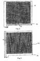
- FIG. 3is a diagram showing the structure of the antenna array of the induction layer in the present invention, which is etched or printed along X-axis;
- FIG. 4is a diagram showing the structure of the antenna array of the induction layer in the present invention, which is etched or printed along Y-axis;
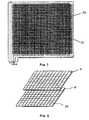
- FIG. 5is a diagram showing massive structure of the induction cells formed by the X-Y directional antenna array of the induction layer in the present invention
- FIG. 6is a diagram showing the structure of two induction layers overlaid one by one according to the present invention.
- FIG. 7is a diagram showing the principle of the generation of the induction signal and identification of the input touch location
- FIG. 8is a diagram showing the connection between the induction layer and the control circuit which are separated according to the present invention.
- FIG. 9is a diagram showing the connection between the output of the antenna array and the corresponding input terminal of the printed substrate (or electrical connection means) according to the present invention.
- FIG. 10is a diagram showing the identification circuit according to the present invention.
- a touch control display screen with built-in membrane antenna array lattice electromagnetic induction layerincludes at least display screen 3 and shell 1 , 7 ; wherein an induction layer 4 is provided in the rear of the display screen 3 , the output of the induction layer 4 is connected to an induction-collection control circuit, a display screen control circuit is also provided in the shell 1 , 7 .
- the display screen 3is a plasma display screen, a liquid-crystal display screen or other flat display screen.
- the induction layer 4is provided after the display screen 3 , and the induction layer 4 can also induce the touch position of the handwriting through the display screen.
- the area of the induction layer 4is same as the area of the display screen 3 .
- a shield layer 5is provided after the induction layer 4
- a display screen control circuit 6is provided after the shield layer 5 .
- the shield layer 5is insulated and shielded with induction layer 4 and display screen control circuit 6 respectively.
- the shield layer 5 and the display screen control circuit 6may be provided in other space of the display screen or main unit.
- the conjunction of the shield layer 5 with the display screen control circuit 6 and induction layer 4 by means of overlaying each otheris advantageous to concentrate the whole induction device.
- a spaceis provided between the shield layer 5 and display screen control circuit 6 , in order to further ensure the shield effect.
- the shield layer 5can has no insulating layer material thereon.
- the shield layer 5is used to enhance the anti-interference ability of the device.
- a transparent protecting layer or a protecting film 2is provided in the front of the display screen 3 , in order to improve anti-wear performance of the surface of the display screen 3 and so on.
- a buffering layer 8 ′is provided between the induction layer 4 and the shield layer 5 , or a buffering layer 8 ′ is provided between the induction layer 4 and the shield layer 5 .
- the buffering layeris used to keep a reasonable space between the induction layer 4 and the shield layer 5 .
- the electromagnetic signalis transmitted from the pen in the both cases that the pen is pressed down and the pen is not pressed down, so as to control conveniently.
- the electromagnetic signalis not transmitted in the case that the pen is not pressed down.
- the pencan be provided with pressure induction means in order to sensing the pressure by using different frequency.
- the area of the induction layer 4may be smaller than the area of the display screen 3 , and the induction layer 4 may be positioned in one or two or four sides of the display screen 3 .
- the area of the induction layer 4may be larger than the area of the display screen 3 , so the whole display screen 3 and the periphery of the display screen 3 possess the capability of touch-operation.
- the induction layer 4may be the antenna array 52 , 51 printed on the insulation membrane 55 and arranged along the X, Y axes, therein the area enclosed by each lattice unit constitutes one induction cell 53 .
- the insulation membrane 55may be film material in order to cut the cost.
- the induction layer 5may be the antenna array formed by etching the copper-platinum covering the insulation membrane 55 , may be the antenna array formed by flexible printed circuitry (FPC), and may be the antenna array formed by the silver-plasm or the mixture material of the silver-plasm and the carbon-plasm which is printed on the insulation membrane.
- FPCflexible printed circuitry
- the induction layercan be printed on two surfaces of the insulation membrane, or printed on one surface of the insulation membrane, and there are two layers of insulation membrane in which one is overlaid on the other.
- two or more induction layers 4 and 4 ′are overlaid together and the induction cells 53 on each induction layer are set to interlace each other, so as to improve the accuracy of the touch screen.
- the interval sizes of the said induction cells on respective layersmay be same or different.
- the scale unit of the coordinatesis consequentially shorten, so the accuracy of induction is improved.
- the scale unit of the coordinatescan also be shorten, and so the sensitivity of the electronic white board is improved.
- the induction-collection control circuit of the induction layer 4 and the output of the antenna array of the induction layerare integrated by direct connection, the components of the induction-collection control circuit are positioned on the output terminal of the antenna array, and the induction-collection control circuit is positioned in the shell.
- FPCflexible printed circuitry
- the components of the control circuitare mounted on a printed substrate which is separated from the induction layer, the output of the antenna array of the induction layer is connected to the corresponding input terminal on the printed substrate by means of pressure-connection, plug-in connection or welding-connection.
- the specific connection modeis as shown in FIG. 9 , therein the output of the antenna array of the induction layer is positioned between hard sheet 600 and printed substrate 500 .
- the buffering layer 7is provided between the hard sheet 600 and the output of the antenna array.
- the hard sheet 600 , buffering layer 7 and the output of the antenna arrayare overlaid on the printed substrate 500 by means of the screwing-conjunction of the screw 700 .
- the output of the antenna arrayis connected with the corresponding input terminal 511 ′ of the printed substrate 500 .
- the printed substratemay be the printed substrate of the display screen control circuit in the body of the display screen. Therefore, the control components can be concentrated, the number of module can be reduced, and the cost can be cut.
- the printed substratemay be the printed substrate of the display screen control circuit outside the body of the display screen, or a self contained unit, otherwise it may be set on the main board of PC.
- the connection between themis achieved by line or cable.
- the induction control circuitis positioned outside the body, and connected to the body through the electrical connection means.
- the output of the antenna array of the induction layeris connected with the output interface of the induction layer by means of pressure connection, plug-in connection, or welding-connection.
- On the control circuitan interface which can match the electrical connection means of the induction layer is provided.
- the specific connection modeis shown in FIG. 8 .
- the components of the induction-collection control circuitcan be also provided on the printed substrate 8 which is separated from the induction layer 4 but integrated with the display screen control circuit. Certainly, they can be provided outside the body of the display screen, for example, they can be set in a PC.
- the output 82 of the antenna array of the induction layeris connected with the corresponding input terminal 81 of the printed substrate by means of pressure connection, plug-in connection or welding-connection.
- the connection interfacemay be the existing universal standard interface, for example, the output interface 82 of the induction layer and the interface 81 of the control circuit may be one of the following: pin-type connection means, flexible printed circuitry means, PIN-PIN connection means, welding spot (VGA) thermal-melted connection means, ultrasonic welding device, solder-plate welding device, puncture-type connection means.
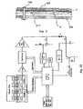
- the touch-control mechanism of the present inventionis as shown in FIG. 7 .
- Pis the signal input terminal of the pen, and there is a bigger conductor p′ on the head of the pen.
- the electromagnetic pentransmits electromagnetic signal continuously.
- said electromagnetic signalpasses through the induction antenna at the corresponding location, then the antenna at this location induces a signal.
- the location signal induced by the induction generation deviceis transferred to the input terminal of the control identification circuit through the wire lead on X, Y direction.
- the resultant location signalis transferred to the processing circuit and calculated by the CPU, so as to determine the location coordinates of the electromagnetic signal on the induction antenna and various operation statuses.
- Above data or informationis sent to a computer, whereby to control the computer to identify, display, record and so on.
- a Z-axis directed pressure sensoris provided in the tail of the pen-point, and the output of the sensor is connect to the control terminal of the electromagnetic wave generation device. So the transmitted electromagnetic wave signal can be changed by the pressure-touching, thereby the pressure (input signal) of the pen-point can be identified more reliably.
- the electromagnetic operating-penis the electromagnetic signal resource for induction, when the devise according to the present invention is in use.
- the electromagnetic handwriting operating-pentransmits frequency-fixed signal or data electromagnetic signal continuously.
- the electromagnetic fieldpasses through the antenna array, and the electromagnetic signal is induced by the corresponding underlayer horizontal antenna and top-layer vertical antenna in the center and neighborhood of the electromagnetic signal resource.
- the electromagnetic signalis transferred to CPU via identification circuit interface.
- the CPUcalculates and compares the location and voltage value of the induction antenna, frequency signal changes, and determines the location of the electromagnetic signal resource and various operation statuses, then transfers the result to PC so as to control the PC to perform various operation commands.
- Said operationis, for example, identifying for character or pattern, drawing and calling for shortcut key, and so on.
- the electromagnetic pentransmits electromagnetic signal continuously.
- said electromagnetic signalpasses through the induction antenna at the corresponding location, then the antenna at this location induces a signal.
- the location signal induced by the induction generation deviceis transferred to the input terminal of the control identification circuit through the wire lead on X, Y direction.
- the resultant location signalis transferred to the CPU of the processing circuit to calculate, so as to determine the location coordinates of the electromagnetic signal on the induction antenna and various operation statuses.
- Above data or informationis sent to a computer, whereby to control the computer to identify, display, record and so on.
- a Z-axis directed pressure sensoris provided in the tail of the pen-point, and the output of the sensor is connect to the control terminal of the electromagnetic wave generation device. So the transmitted electromagnetic wave signal can be changed by the pressure-touching, thereby the pressure (input signal) of the pen-point can be identified more reliably.
- the present inventioncan be widely applied to various touch control equipment. Meanwhile, the idea of the present invention is not limited in the incorporation of the electromagnetic induction layer and flat display screen, but the electromagnetic induction layer can be provided in the rear of other non-CRT display screen, such as nonplanar plasma display screen and nonplanar liquid-crystal display screen with various profile, so as to realize the touch screen with low cost.
Landscapes
- Engineering & Computer Science (AREA)
- General Engineering & Computer Science (AREA)
- Theoretical Computer Science (AREA)
- Physics & Mathematics (AREA)
- Human Computer Interaction (AREA)
- General Physics & Mathematics (AREA)
- Electromagnetism (AREA)
- Position Input By Displaying (AREA)
- Devices For Indicating Variable Information By Combining Individual Elements (AREA)
Abstract
Description
Claims (10)
Applications Claiming Priority (7)
| Application Number | Priority Date | Filing Date | Title |
|---|---|---|---|
| CN01279677.8UCN2512043Y (en) | 2001-12-29 | 2001-12-29 | Electronic whiteboard with flexible diaphragm type electromagnetic induction generating device |
| CN01279677.8 | 2001-12-29 | ||
| CN01279677U | 2001-12-29 | ||
| CN 02257335CN2569259Y (en) | 2002-09-16 | 2002-09-16 | Touch control display with built-in diaphragm antenna array grid electromagnetic induction layer |
| CN02257335U | 2002-09-16 | ||
| CN02257335.6 | 2002-09-16 | ||
| PCT/CN2002/000687WO2003056422A1 (en) | 2001-12-29 | 2002-09-27 | A touch control display screen with a built-in electromagnet induction layer of septum array grids |
Publications (2)
| Publication Number | Publication Date |
|---|---|
| US20050062725A1 US20050062725A1 (en) | 2005-03-24 |
| US7796122B2true US7796122B2 (en) | 2010-09-14 |
Family
ID=25741085
Family Applications (1)
| Application Number | Title | Priority Date | Filing Date |
|---|---|---|---|
| US10/500,438Active2026-04-08US7796122B2 (en) | 2001-12-29 | 2002-09-27 | Touch control display screen with a built-in electromagnet induction layer of septum array grids |
Country Status (6)
| Country | Link |
|---|---|
| US (1) | US7796122B2 (en) |
| EP (1) | EP1469383A4 (en) |
| JP (1) | JP2005513575A (en) |
| KR (1) | KR100605901B1 (en) |
| AU (1) | AU2002338134A1 (en) |
| WO (1) | WO2003056422A1 (en) |
Cited By (131)
| Publication number | Priority date | Publication date | Assignee | Title |
|---|---|---|---|---|
| US20080303774A1 (en)* | 2003-12-08 | 2008-12-11 | Canono Kabushiki Kaisha | Display Apparatus |
| US20100265203A1 (en)* | 2009-04-20 | 2010-10-21 | Broadcom Corporation | Dual mode inductive touch screen for use in a configurable communication device and methods for use therewith |
| US20100265189A1 (en)* | 2009-04-20 | 2010-10-21 | Broadcom Corporation | Inductive touch screen with integrated antenna for use in a communication device and methods for use therewith |
| US20100265190A1 (en)* | 2009-04-20 | 2010-10-21 | Broadcom Corporation | Inductive touch screen and methods for use therewith |
| US20110102331A1 (en)* | 2009-10-29 | 2011-05-05 | Qrg Limited | Redundant touchscreen electrodes |
| US20110163964A1 (en)* | 2010-01-07 | 2011-07-07 | Yen-Lung Tsai & Tsung-Chieh CHO | Dual type touch display device |
| US20120034888A1 (en)* | 2010-08-05 | 2012-02-09 | Franco De Flaviis | Method and System for Utilizing a Touchscreen Interface as an Antenna |
| US9667317B2 (en) | 2015-06-15 | 2017-05-30 | At&T Intellectual Property I, L.P. | Method and apparatus for providing security using network traffic adjustments |
| US9674711B2 (en) | 2013-11-06 | 2017-06-06 | At&T Intellectual Property I, L.P. | Surface-wave communications and methods thereof |
| US9685992B2 (en) | 2014-10-03 | 2017-06-20 | At&T Intellectual Property I, L.P. | Circuit panel network and methods thereof |
| US9705610B2 (en) | 2014-10-21 | 2017-07-11 | At&T Intellectual Property I, L.P. | Transmission device with impairment compensation and methods for use therewith |
| US9705561B2 (en) | 2015-04-24 | 2017-07-11 | At&T Intellectual Property I, L.P. | Directional coupling device and methods for use therewith |
| US9722318B2 (en) | 2015-07-14 | 2017-08-01 | At&T Intellectual Property I, L.P. | Method and apparatus for coupling an antenna to a device |
| US9729197B2 (en) | 2015-10-01 | 2017-08-08 | At&T Intellectual Property I, L.P. | Method and apparatus for communicating network management traffic over a network |
| US9735833B2 (en) | 2015-07-31 | 2017-08-15 | At&T Intellectual Property I, L.P. | Method and apparatus for communications management in a neighborhood network |
| US9742462B2 (en) | 2014-12-04 | 2017-08-22 | At&T Intellectual Property I, L.P. | Transmission medium and communication interfaces and methods for use therewith |
| US9742521B2 (en) | 2014-11-20 | 2017-08-22 | At&T Intellectual Property I, L.P. | Transmission device with mode division multiplexing and methods for use therewith |
| US9749053B2 (en) | 2015-07-23 | 2017-08-29 | At&T Intellectual Property I, L.P. | Node device, repeater and methods for use therewith |
| US9748626B2 (en) | 2015-05-14 | 2017-08-29 | At&T Intellectual Property I, L.P. | Plurality of cables having different cross-sectional shapes which are bundled together to form a transmission medium |
| US9749013B2 (en) | 2015-03-17 | 2017-08-29 | At&T Intellectual Property I, L.P. | Method and apparatus for reducing attenuation of electromagnetic waves guided by a transmission medium |
| US9769128B2 (en) | 2015-09-28 | 2017-09-19 | At&T Intellectual Property I, L.P. | Method and apparatus for encryption of communications over a network |
| US9769020B2 (en) | 2014-10-21 | 2017-09-19 | At&T Intellectual Property I, L.P. | Method and apparatus for responding to events affecting communications in a communication network |
| US9768833B2 (en) | 2014-09-15 | 2017-09-19 | At&T Intellectual Property I, L.P. | Method and apparatus for sensing a condition in a transmission medium of electromagnetic waves |
| US9780834B2 (en) | 2014-10-21 | 2017-10-03 | At&T Intellectual Property I, L.P. | Method and apparatus for transmitting electromagnetic waves |
| US9787412B2 (en) | 2015-06-25 | 2017-10-10 | At&T Intellectual Property I, L.P. | Methods and apparatus for inducing a fundamental wave mode on a transmission medium |
| US9793951B2 (en) | 2015-07-15 | 2017-10-17 | At&T Intellectual Property I, L.P. | Method and apparatus for launching a wave mode that mitigates interference |
| US9793954B2 (en) | 2015-04-28 | 2017-10-17 | At&T Intellectual Property I, L.P. | Magnetic coupling device and methods for use therewith |
| US9793955B2 (en) | 2015-04-24 | 2017-10-17 | At&T Intellectual Property I, Lp | Passive electrical coupling device and methods for use therewith |
| US9800327B2 (en) | 2014-11-20 | 2017-10-24 | At&T Intellectual Property I, L.P. | Apparatus for controlling operations of a communication device and methods thereof |
| US9820146B2 (en) | 2015-06-12 | 2017-11-14 | At&T Intellectual Property I, L.P. | Method and apparatus for authentication and identity management of communicating devices |
| US9838896B1 (en) | 2016-12-09 | 2017-12-05 | At&T Intellectual Property I, L.P. | Method and apparatus for assessing network coverage |
| US9838078B2 (en) | 2015-07-31 | 2017-12-05 | At&T Intellectual Property I, L.P. | Method and apparatus for exchanging communication signals |
| US9847566B2 (en) | 2015-07-14 | 2017-12-19 | At&T Intellectual Property I, L.P. | Method and apparatus for adjusting a field of a signal to mitigate interference |
| US9847850B2 (en) | 2014-10-14 | 2017-12-19 | At&T Intellectual Property I, L.P. | Method and apparatus for adjusting a mode of communication in a communication network |
| US9853342B2 (en) | 2015-07-14 | 2017-12-26 | At&T Intellectual Property I, L.P. | Dielectric transmission medium connector and methods for use therewith |
| US9860075B1 (en) | 2016-08-26 | 2018-01-02 | At&T Intellectual Property I, L.P. | Method and communication node for broadband distribution |
| US9866276B2 (en) | 2014-10-10 | 2018-01-09 | At&T Intellectual Property I, L.P. | Method and apparatus for arranging communication sessions in a communication system |
| US9866309B2 (en) | 2015-06-03 | 2018-01-09 | At&T Intellectual Property I, Lp | Host node device and methods for use therewith |
| US9865911B2 (en) | 2015-06-25 | 2018-01-09 | At&T Intellectual Property I, L.P. | Waveguide system for slot radiating first electromagnetic waves that are combined into a non-fundamental wave mode second electromagnetic wave on a transmission medium |
| US9871558B2 (en) | 2014-10-21 | 2018-01-16 | At&T Intellectual Property I, L.P. | Guided-wave transmission device and methods for use therewith |
| US9871282B2 (en) | 2015-05-14 | 2018-01-16 | At&T Intellectual Property I, L.P. | At least one transmission medium having a dielectric surface that is covered at least in part by a second dielectric |
| US9871283B2 (en) | 2015-07-23 | 2018-01-16 | At&T Intellectual Property I, Lp | Transmission medium having a dielectric core comprised of plural members connected by a ball and socket configuration |
| US9876605B1 (en) | 2016-10-21 | 2018-01-23 | At&T Intellectual Property I, L.P. | Launcher and coupling system to support desired guided wave mode |
| US9876571B2 (en) | 2015-02-20 | 2018-01-23 | At&T Intellectual Property I, Lp | Guided-wave transmission device with non-fundamental mode propagation and methods for use therewith |
| US9876264B2 (en) | 2015-10-02 | 2018-01-23 | At&T Intellectual Property I, Lp | Communication system, guided wave switch and methods for use therewith |
| US9882257B2 (en) | 2015-07-14 | 2018-01-30 | At&T Intellectual Property I, L.P. | Method and apparatus for launching a wave mode that mitigates interference |
| US9887447B2 (en) | 2015-05-14 | 2018-02-06 | At&T Intellectual Property I, L.P. | Transmission medium having multiple cores and methods for use therewith |
| US9893795B1 (en) | 2016-12-07 | 2018-02-13 | At&T Intellectual Property I, Lp | Method and repeater for broadband distribution |
| US9906269B2 (en) | 2014-09-17 | 2018-02-27 | At&T Intellectual Property I, L.P. | Monitoring and mitigating conditions in a communication network |
| US9904535B2 (en) | 2015-09-14 | 2018-02-27 | At&T Intellectual Property I, L.P. | Method and apparatus for distributing software |
| US9913139B2 (en) | 2015-06-09 | 2018-03-06 | At&T Intellectual Property I, L.P. | Signal fingerprinting for authentication of communicating devices |
| US9912033B2 (en) | 2014-10-21 | 2018-03-06 | At&T Intellectual Property I, Lp | Guided wave coupler, coupling module and methods for use therewith |
| US9912027B2 (en) | 2015-07-23 | 2018-03-06 | At&T Intellectual Property I, L.P. | Method and apparatus for exchanging communication signals |
| US9912381B2 (en) | 2015-06-03 | 2018-03-06 | At&T Intellectual Property I, Lp | Network termination and methods for use therewith |
| US9911020B1 (en) | 2016-12-08 | 2018-03-06 | At&T Intellectual Property I, L.P. | Method and apparatus for tracking via a radio frequency identification device |
| US9917341B2 (en) | 2015-05-27 | 2018-03-13 | At&T Intellectual Property I, L.P. | Apparatus and method for launching electromagnetic waves and for modifying radial dimensions of the propagating electromagnetic waves |
| US9929755B2 (en) | 2015-07-14 | 2018-03-27 | At&T Intellectual Property I, L.P. | Method and apparatus for coupling an antenna to a device |
| US9927517B1 (en) | 2016-12-06 | 2018-03-27 | At&T Intellectual Property I, L.P. | Apparatus and methods for sensing rainfall |
| US9948333B2 (en) | 2015-07-23 | 2018-04-17 | At&T Intellectual Property I, L.P. | Method and apparatus for wireless communications to mitigate interference |
| US9954286B2 (en) | 2014-10-21 | 2018-04-24 | At&T Intellectual Property I, L.P. | Guided-wave transmission device with non-fundamental mode propagation and methods for use therewith |
| US9954287B2 (en) | 2014-11-20 | 2018-04-24 | At&T Intellectual Property I, L.P. | Apparatus for converting wireless signals and electromagnetic waves and methods thereof |
| US9967173B2 (en) | 2015-07-31 | 2018-05-08 | At&T Intellectual Property I, L.P. | Method and apparatus for authentication and identity management of communicating devices |
| US9973416B2 (en) | 2014-10-02 | 2018-05-15 | At&T Intellectual Property I, L.P. | Method and apparatus that provides fault tolerance in a communication network |
| US9973940B1 (en) | 2017-02-27 | 2018-05-15 | At&T Intellectual Property I, L.P. | Apparatus and methods for dynamic impedance matching of a guided wave launcher |
| US9991580B2 (en) | 2016-10-21 | 2018-06-05 | At&T Intellectual Property I, L.P. | Launcher and coupling system for guided wave mode cancellation |
| US9999038B2 (en) | 2013-05-31 | 2018-06-12 | At&T Intellectual Property I, L.P. | Remote distributed antenna system |
| US9998870B1 (en) | 2016-12-08 | 2018-06-12 | At&T Intellectual Property I, L.P. | Method and apparatus for proximity sensing |
| US9997819B2 (en) | 2015-06-09 | 2018-06-12 | At&T Intellectual Property I, L.P. | Transmission medium and method for facilitating propagation of electromagnetic waves via a core |
| US10009067B2 (en) | 2014-12-04 | 2018-06-26 | At&T Intellectual Property I, L.P. | Method and apparatus for configuring a communication interface |
| US10020844B2 (en) | 2016-12-06 | 2018-07-10 | T&T Intellectual Property I, L.P. | Method and apparatus for broadcast communication via guided waves |
| US10027397B2 (en) | 2016-12-07 | 2018-07-17 | At&T Intellectual Property I, L.P. | Distributed antenna system and methods for use therewith |
| US10044409B2 (en) | 2015-07-14 | 2018-08-07 | At&T Intellectual Property I, L.P. | Transmission medium and methods for use therewith |
| US10051630B2 (en) | 2013-05-31 | 2018-08-14 | At&T Intellectual Property I, L.P. | Remote distributed antenna system |
| US10069535B2 (en) | 2016-12-08 | 2018-09-04 | At&T Intellectual Property I, L.P. | Apparatus and methods for launching electromagnetic waves having a certain electric field structure |
| US10069185B2 (en) | 2015-06-25 | 2018-09-04 | At&T Intellectual Property I, L.P. | Methods and apparatus for inducing a non-fundamental wave mode on a transmission medium |
| US10090606B2 (en) | 2015-07-15 | 2018-10-02 | At&T Intellectual Property I, L.P. | Antenna system with dielectric array and methods for use therewith |
| US10090594B2 (en) | 2016-11-23 | 2018-10-02 | At&T Intellectual Property I, L.P. | Antenna system having structural configurations for assembly |
| US10103422B2 (en) | 2016-12-08 | 2018-10-16 | At&T Intellectual Property I, L.P. | Method and apparatus for mounting network devices |
| US10135146B2 (en) | 2016-10-18 | 2018-11-20 | At&T Intellectual Property I, L.P. | Apparatus and methods for launching guided waves via circuits |
| US10135145B2 (en) | 2016-12-06 | 2018-11-20 | At&T Intellectual Property I, L.P. | Apparatus and methods for generating an electromagnetic wave along a transmission medium |
| US10135147B2 (en) | 2016-10-18 | 2018-11-20 | At&T Intellectual Property I, L.P. | Apparatus and methods for launching guided waves via an antenna |
| US10136255B2 (en) | 2016-12-08 | 2018-11-20 | At&T Intellectual Property I, L.P. | Method and apparatus for proximity sensing on a communication device |
| US10139820B2 (en) | 2016-12-07 | 2018-11-27 | At&T Intellectual Property I, L.P. | Method and apparatus for deploying equipment of a communication system |
| US10148016B2 (en) | 2015-07-14 | 2018-12-04 | At&T Intellectual Property I, L.P. | Apparatus and methods for communicating utilizing an antenna array |
| US10168695B2 (en) | 2016-12-07 | 2019-01-01 | At&T Intellectual Property I, L.P. | Method and apparatus for controlling an unmanned aircraft |
| US10178445B2 (en) | 2016-11-23 | 2019-01-08 | At&T Intellectual Property I, L.P. | Methods, devices, and systems for load balancing between a plurality of waveguides |
| US10205655B2 (en) | 2015-07-14 | 2019-02-12 | At&T Intellectual Property I, L.P. | Apparatus and methods for communicating utilizing an antenna array and multiple communication paths |
| US10225025B2 (en) | 2016-11-03 | 2019-03-05 | At&T Intellectual Property I, L.P. | Method and apparatus for detecting a fault in a communication system |
| US10224634B2 (en) | 2016-11-03 | 2019-03-05 | At&T Intellectual Property I, L.P. | Methods and apparatus for adjusting an operational characteristic of an antenna |
| US10243784B2 (en) | 2014-11-20 | 2019-03-26 | At&T Intellectual Property I, L.P. | System for generating topology information and methods thereof |
| US10243270B2 (en) | 2016-12-07 | 2019-03-26 | At&T Intellectual Property I, L.P. | Beam adaptive multi-feed dielectric antenna system and methods for use therewith |
| US10249456B2 (en)* | 2017-03-21 | 2019-04-02 | Illinois Tool Works Inc. | Apparatus with membrane panel having close-proximity communication antenna |
| US10264586B2 (en) | 2016-12-09 | 2019-04-16 | At&T Mobility Ii Llc | Cloud-based packet controller and methods for use therewith |
| US10291334B2 (en) | 2016-11-03 | 2019-05-14 | At&T Intellectual Property I, L.P. | System for detecting a fault in a communication system |
| US10298293B2 (en) | 2017-03-13 | 2019-05-21 | At&T Intellectual Property I, L.P. | Apparatus of communication utilizing wireless network devices |
| US10305190B2 (en) | 2016-12-01 | 2019-05-28 | At&T Intellectual Property I, L.P. | Reflecting dielectric antenna system and methods for use therewith |
| US10312567B2 (en) | 2016-10-26 | 2019-06-04 | At&T Intellectual Property I, L.P. | Launcher with planar strip antenna and methods for use therewith |
| US10320586B2 (en) | 2015-07-14 | 2019-06-11 | At&T Intellectual Property I, L.P. | Apparatus and methods for generating non-interfering electromagnetic waves on an insulated transmission medium |
| US10326689B2 (en) | 2016-12-08 | 2019-06-18 | At&T Intellectual Property I, L.P. | Method and system for providing alternative communication paths |
| US10326494B2 (en) | 2016-12-06 | 2019-06-18 | At&T Intellectual Property I, L.P. | Apparatus for measurement de-embedding and methods for use therewith |
| US10340983B2 (en) | 2016-12-09 | 2019-07-02 | At&T Intellectual Property I, L.P. | Method and apparatus for surveying remote sites via guided wave communications |
| US10340603B2 (en) | 2016-11-23 | 2019-07-02 | At&T Intellectual Property I, L.P. | Antenna system having shielded structural configurations for assembly |
| US10340601B2 (en) | 2016-11-23 | 2019-07-02 | At&T Intellectual Property I, L.P. | Multi-antenna system and methods for use therewith |
| US10340600B2 (en) | 2016-10-18 | 2019-07-02 | At&T Intellectual Property I, L.P. | Apparatus and methods for launching guided waves via plural waveguide systems |
| US10340573B2 (en) | 2016-10-26 | 2019-07-02 | At&T Intellectual Property I, L.P. | Launcher with cylindrical coupling device and methods for use therewith |
| US10355367B2 (en) | 2015-10-16 | 2019-07-16 | At&T Intellectual Property I, L.P. | Antenna structure for exchanging wireless signals |
| US10359749B2 (en) | 2016-12-07 | 2019-07-23 | At&T Intellectual Property I, L.P. | Method and apparatus for utilities management via guided wave communication |
| US10361489B2 (en) | 2016-12-01 | 2019-07-23 | At&T Intellectual Property I, L.P. | Dielectric dish antenna system and methods for use therewith |
| US10374316B2 (en) | 2016-10-21 | 2019-08-06 | At&T Intellectual Property I, L.P. | System and dielectric antenna with non-uniform dielectric |
| US10382976B2 (en) | 2016-12-06 | 2019-08-13 | At&T Intellectual Property I, L.P. | Method and apparatus for managing wireless communications based on communication paths and network device positions |
| US10389029B2 (en) | 2016-12-07 | 2019-08-20 | At&T Intellectual Property I, L.P. | Multi-feed dielectric antenna system with core selection and methods for use therewith |
| US10389037B2 (en) | 2016-12-08 | 2019-08-20 | At&T Intellectual Property I, L.P. | Apparatus and methods for selecting sections of an antenna array and use therewith |
| US10411356B2 (en) | 2016-12-08 | 2019-09-10 | At&T Intellectual Property I, L.P. | Apparatus and methods for selectively targeting communication devices with an antenna array |
| US10439675B2 (en) | 2016-12-06 | 2019-10-08 | At&T Intellectual Property I, L.P. | Method and apparatus for repeating guided wave communication signals |
| US10446936B2 (en) | 2016-12-07 | 2019-10-15 | At&T Intellectual Property I, L.P. | Multi-feed dielectric antenna system and methods for use therewith |
| US10498044B2 (en) | 2016-11-03 | 2019-12-03 | At&T Intellectual Property I, L.P. | Apparatus for configuring a surface of an antenna |
| US10530505B2 (en) | 2016-12-08 | 2020-01-07 | At&T Intellectual Property I, L.P. | Apparatus and methods for launching electromagnetic waves along a transmission medium |
| US10535928B2 (en) | 2016-11-23 | 2020-01-14 | At&T Intellectual Property I, L.P. | Antenna system and methods for use therewith |
| US10547348B2 (en) | 2016-12-07 | 2020-01-28 | At&T Intellectual Property I, L.P. | Method and apparatus for switching transmission mediums in a communication system |
| US10601494B2 (en) | 2016-12-08 | 2020-03-24 | At&T Intellectual Property I, L.P. | Dual-band communication device and method for use therewith |
| US10637149B2 (en) | 2016-12-06 | 2020-04-28 | At&T Intellectual Property I, L.P. | Injection molded dielectric antenna and methods for use therewith |
| US10650940B2 (en) | 2015-05-15 | 2020-05-12 | At&T Intellectual Property I, L.P. | Transmission medium having a conductive material and methods for use therewith |
| US10694379B2 (en) | 2016-12-06 | 2020-06-23 | At&T Intellectual Property I, L.P. | Waveguide system with device-based authentication and methods for use therewith |
| US10727599B2 (en) | 2016-12-06 | 2020-07-28 | At&T Intellectual Property I, L.P. | Launcher with slot antenna and methods for use therewith |
| US10755542B2 (en) | 2016-12-06 | 2020-08-25 | At&T Intellectual Property I, L.P. | Method and apparatus for surveillance via guided wave communication |
| US10777873B2 (en) | 2016-12-08 | 2020-09-15 | At&T Intellectual Property I, L.P. | Method and apparatus for mounting network devices |
| US10797781B2 (en) | 2015-06-03 | 2020-10-06 | At&T Intellectual Property I, L.P. | Client node device and methods for use therewith |
| US10811767B2 (en) | 2016-10-21 | 2020-10-20 | At&T Intellectual Property I, L.P. | System and dielectric antenna with convex dielectric radome |
| US10819035B2 (en) | 2016-12-06 | 2020-10-27 | At&T Intellectual Property I, L.P. | Launcher with helical antenna and methods for use therewith |
| US10916969B2 (en) | 2016-12-08 | 2021-02-09 | At&T Intellectual Property I, L.P. | Method and apparatus for providing power using an inductive coupling |
| US10938108B2 (en) | 2016-12-08 | 2021-03-02 | At&T Intellectual Property I, L.P. | Frequency selective multi-feed dielectric antenna system and methods for use therewith |
Families Citing this family (17)
| Publication number | Priority date | Publication date | Assignee | Title |
|---|---|---|---|---|
| CN2512043Y (en)* | 2001-12-29 | 2002-09-18 | 台均实业有限公司 | Electronic whiteboard with flexible diaphragm type electromagnetic induction generating device |
| US7450109B2 (en)* | 2004-07-13 | 2008-11-11 | International Business Machines Corporation | Electronic whiteboard |
| US7436394B2 (en)* | 2004-07-13 | 2008-10-14 | International Business Machines Corporation | Apparatus, system and method of importing data arranged in a table on an electronic whiteboard into a spreadsheet |
| TWI261276B (en)* | 2005-05-13 | 2006-09-01 | Tatung Co | Touch-control acrylic-board manufacturing method |
| KR100948050B1 (en)* | 2006-11-23 | 2010-03-19 | 주식회사 메디슨 | Portable ultrasound system |
| US8456851B2 (en)* | 2008-05-16 | 2013-06-04 | Apple Inc. | Flex circuit with single sided routing and double sided attach |
| CN102053408B (en)* | 2009-11-05 | 2013-04-10 | 太瀚科技股份有限公司 | Composite substrate and display with electromagnetic induction loop |
| DE102010014796A1 (en) | 2010-02-03 | 2011-08-04 | Emerging Display Technologies Corp. | Screen unit with a touch screen |
| US9184502B2 (en) | 2010-12-22 | 2015-11-10 | Intel Corporation | Antenna integrated into a touch sensor of a touchscreen display |
| US20130234959A1 (en) | 2012-03-06 | 2013-09-12 | Industry-University Cooperation Foundation Hanyang University | System and method for linking and controlling terminals |
| US8918565B2 (en)* | 2012-05-19 | 2014-12-23 | Robert Dennis Kennedy | Tablet computer screen and mobile phone screen to digital I/O converter |
| CN104571772A (en)* | 2013-10-12 | 2015-04-29 | 上海和辉光电有限公司 | Electromagnetic touch screen structure |
| KR102175750B1 (en)* | 2014-10-29 | 2020-11-06 | 삼성전자주식회사 | Antenna device for electronic device with the same |
| CN106487964B (en)* | 2016-12-30 | 2019-08-02 | 信利光电股份有限公司 | A kind of mobile terminal and its back shroud |
| US10489003B1 (en)* | 2018-06-29 | 2019-11-26 | Pixart Imaging Inc. | Capacitive touch control device, electricity charging controller, and electricity charged controller |
| CN111323111B (en)* | 2020-03-11 | 2022-04-22 | 北京空间飞行器总体设计部 | A modal test system suitable for thin film antenna in vacuum environment |
| CN111766985B (en)* | 2020-06-23 | 2025-01-10 | Oppo广东移动通信有限公司 | Display modules, electronic devices, and touch control systems |
Citations (15)
| Publication number | Priority date | Publication date | Assignee | Title |
|---|---|---|---|---|
| US4933544A (en)* | 1988-01-29 | 1990-06-12 | Sony Corporation | Touch entry apparatus for cathode ray tube with non-perpendicular detection beams |
| USRE33740E (en)* | 1984-12-28 | 1991-11-12 | Wacom Co., Ltd. | Position detecting device |
| US5381160A (en)* | 1991-09-27 | 1995-01-10 | Calcomp Inc. | See-through digitizer with clear conductive grid |
| US5428417A (en)* | 1993-08-02 | 1995-06-27 | Lichtenstein; Bernard | Visual lecture aid |
| US6137427A (en)* | 1994-04-05 | 2000-10-24 | Binstead; Ronald Peter | Multiple input proximity detector and touchpad system |
| US6249234B1 (en)* | 1994-05-14 | 2001-06-19 | Absolute Sensors Limited | Position detector |
| US20020000977A1 (en)* | 2000-03-23 | 2002-01-03 | National Aeronautics And Space Administration | Three dimensional interactive display |
| US20020063694A1 (en)* | 1998-11-20 | 2002-05-30 | Leroy Bertrand Keely, Jr. | Pen-based computer system |
| US6417813B1 (en)* | 2000-10-31 | 2002-07-09 | Harris Corporation | Feedthrough lens antenna and associated methods |
| US6434403B1 (en)* | 1999-02-19 | 2002-08-13 | Bodycom, Inc. | Personal digital assistant with wireless telephone |
| US20030122774A1 (en)* | 1999-09-10 | 2003-07-03 | Fujitsu Limited | Input processing method and input processing device for implementing same |
| US6661409B2 (en)* | 2001-08-22 | 2003-12-09 | Motorola, Inc. | Automatically scrolling handwritten input user interface for personal digital assistants and the like |
| US20040239642A1 (en)* | 2001-09-25 | 2004-12-02 | Xuanming Shi | Panel display screen with touch control function |
| US7084933B2 (en)* | 2002-11-14 | 2006-08-01 | Lg.Philips Lcd Co., Ltd. | Touch panel for display device |
| US7113175B2 (en)* | 2000-09-26 | 2006-09-26 | Intertact Corporation | Methods and apparatus for supplying power to touch input devices in a touch sensing system |
Family Cites Families (15)
| Publication number | Priority date | Publication date | Assignee | Title |
|---|---|---|---|---|
| JPS62160525A (en)* | 1986-01-09 | 1987-07-16 | Graphtec Corp | Coordinates position determining device |
| JPS6370326A (en)* | 1986-09-12 | 1988-03-30 | Wacom Co Ltd | Position detector |
| KR0122737B1 (en)* | 1987-12-25 | 1997-11-20 | 후루다 모또오 | Position detection device |
| US5038142A (en)* | 1989-03-14 | 1991-08-06 | International Business Machines Corporation | Touch sensing display screen apparatus |
| JPH0619608A (en)* | 1991-03-15 | 1994-01-28 | Nippon Business Syst Kk | Coordinate input device |
| US5218174A (en)* | 1991-10-01 | 1993-06-08 | Kurta Corporation | Low power cordless magnetic field digitizer with differential grid sensing and synchronous position demodulation |
| US5218173A (en)* | 1991-10-17 | 1993-06-08 | Ibm Corporation | Shielding materials for electromagnetic digitizers |
| JPH05165024A (en)* | 1991-12-18 | 1993-06-29 | Sanyo Electric Co Ltd | Display device |
| JPH0667784A (en)* | 1992-08-21 | 1994-03-11 | Dainippon Printing Co Ltd | Conductive tablet material |
| JP3001394B2 (en)* | 1995-03-10 | 2000-01-24 | 株式会社ワコム | Sensor coil pattern and coordinate input device |
| US5949501A (en)* | 1996-02-13 | 1999-09-07 | Kabushiki Kaisha Pilot | Coordinates input device using liquid crystal sheet |
| JPH10288766A (en)* | 1997-04-15 | 1998-10-27 | Seiko Epson Corp | Liquid crystal display device and electronic device provided with tablet for position input |
| JP2000112639A (en)* | 1998-10-06 | 2000-04-21 | Nippon Graphite Industries Ltd | Coordinate input device |
| EP1135745B1 (en)* | 1998-11-27 | 2003-09-24 | Synaptics (UK) Limited | Position sensor |
| JP2001282443A (en)* | 2000-03-31 | 2001-10-12 | Brother Ind Ltd | Coordinate reading device |
- 2002
- 2002-09-27EPEP02771991Apatent/EP1469383A4/ennot_activeCeased
- 2002-09-27WOPCT/CN2002/000687patent/WO2003056422A1/enactiveApplication Filing
- 2002-09-27AUAU2002338134Apatent/AU2002338134A1/ennot_activeAbandoned
- 2002-09-27JPJP2003556879Apatent/JP2005513575A/enactivePending
- 2002-09-27USUS10/500,438patent/US7796122B2/enactiveActive
- 2002-09-27KRKR1020047010248Apatent/KR100605901B1/ennot_activeExpired - Fee Related
Patent Citations (15)
| Publication number | Priority date | Publication date | Assignee | Title |
|---|---|---|---|---|
| USRE33740E (en)* | 1984-12-28 | 1991-11-12 | Wacom Co., Ltd. | Position detecting device |
| US4933544A (en)* | 1988-01-29 | 1990-06-12 | Sony Corporation | Touch entry apparatus for cathode ray tube with non-perpendicular detection beams |
| US5381160A (en)* | 1991-09-27 | 1995-01-10 | Calcomp Inc. | See-through digitizer with clear conductive grid |
| US5428417A (en)* | 1993-08-02 | 1995-06-27 | Lichtenstein; Bernard | Visual lecture aid |
| US6137427A (en)* | 1994-04-05 | 2000-10-24 | Binstead; Ronald Peter | Multiple input proximity detector and touchpad system |
| US6249234B1 (en)* | 1994-05-14 | 2001-06-19 | Absolute Sensors Limited | Position detector |
| US20020063694A1 (en)* | 1998-11-20 | 2002-05-30 | Leroy Bertrand Keely, Jr. | Pen-based computer system |
| US6434403B1 (en)* | 1999-02-19 | 2002-08-13 | Bodycom, Inc. | Personal digital assistant with wireless telephone |
| US20030122774A1 (en)* | 1999-09-10 | 2003-07-03 | Fujitsu Limited | Input processing method and input processing device for implementing same |
| US20020000977A1 (en)* | 2000-03-23 | 2002-01-03 | National Aeronautics And Space Administration | Three dimensional interactive display |
| US7113175B2 (en)* | 2000-09-26 | 2006-09-26 | Intertact Corporation | Methods and apparatus for supplying power to touch input devices in a touch sensing system |
| US6417813B1 (en)* | 2000-10-31 | 2002-07-09 | Harris Corporation | Feedthrough lens antenna and associated methods |
| US6661409B2 (en)* | 2001-08-22 | 2003-12-09 | Motorola, Inc. | Automatically scrolling handwritten input user interface for personal digital assistants and the like |
| US20040239642A1 (en)* | 2001-09-25 | 2004-12-02 | Xuanming Shi | Panel display screen with touch control function |
| US7084933B2 (en)* | 2002-11-14 | 2006-08-01 | Lg.Philips Lcd Co., Ltd. | Touch panel for display device |
Cited By (152)
| Publication number | Priority date | Publication date | Assignee | Title |
|---|---|---|---|---|
| US8416174B2 (en)* | 2003-12-08 | 2013-04-09 | Canon Kabushiki Kaisha | Display apparatus |
| US20080303774A1 (en)* | 2003-12-08 | 2008-12-11 | Canono Kabushiki Kaisha | Display Apparatus |
| US20100265203A1 (en)* | 2009-04-20 | 2010-10-21 | Broadcom Corporation | Dual mode inductive touch screen for use in a configurable communication device and methods for use therewith |
| US20100265189A1 (en)* | 2009-04-20 | 2010-10-21 | Broadcom Corporation | Inductive touch screen with integrated antenna for use in a communication device and methods for use therewith |
| US20100265190A1 (en)* | 2009-04-20 | 2010-10-21 | Broadcom Corporation | Inductive touch screen and methods for use therewith |
| US8810523B2 (en)* | 2009-04-20 | 2014-08-19 | Broadcom Corporation | Inductive touch screen and methods for use therewith |
| US8339372B2 (en)* | 2009-04-20 | 2012-12-25 | Broadcom Corporation | Inductive touch screen with integrated antenna for use in a communication device and methods for use therewith |
| US8400419B2 (en)* | 2009-04-20 | 2013-03-19 | Broadcom Corporation | Dual mode inductive touch screen for use in a configurable communication device and methods for use therewith |
| US20110102331A1 (en)* | 2009-10-29 | 2011-05-05 | Qrg Limited | Redundant touchscreen electrodes |
| US20110163964A1 (en)* | 2010-01-07 | 2011-07-07 | Yen-Lung Tsai & Tsung-Chieh CHO | Dual type touch display device |
| US20120034888A1 (en)* | 2010-08-05 | 2012-02-09 | Franco De Flaviis | Method and System for Utilizing a Touchscreen Interface as an Antenna |
| US10051630B2 (en) | 2013-05-31 | 2018-08-14 | At&T Intellectual Property I, L.P. | Remote distributed antenna system |
| US9999038B2 (en) | 2013-05-31 | 2018-06-12 | At&T Intellectual Property I, L.P. | Remote distributed antenna system |
| US9674711B2 (en) | 2013-11-06 | 2017-06-06 | At&T Intellectual Property I, L.P. | Surface-wave communications and methods thereof |
| US9768833B2 (en) | 2014-09-15 | 2017-09-19 | At&T Intellectual Property I, L.P. | Method and apparatus for sensing a condition in a transmission medium of electromagnetic waves |
| US10063280B2 (en) | 2014-09-17 | 2018-08-28 | At&T Intellectual Property I, L.P. | Monitoring and mitigating conditions in a communication network |
| US9906269B2 (en) | 2014-09-17 | 2018-02-27 | At&T Intellectual Property I, L.P. | Monitoring and mitigating conditions in a communication network |
| US9973416B2 (en) | 2014-10-02 | 2018-05-15 | At&T Intellectual Property I, L.P. | Method and apparatus that provides fault tolerance in a communication network |
| US9685992B2 (en) | 2014-10-03 | 2017-06-20 | At&T Intellectual Property I, L.P. | Circuit panel network and methods thereof |
| US9866276B2 (en) | 2014-10-10 | 2018-01-09 | At&T Intellectual Property I, L.P. | Method and apparatus for arranging communication sessions in a communication system |
| US9847850B2 (en) | 2014-10-14 | 2017-12-19 | At&T Intellectual Property I, L.P. | Method and apparatus for adjusting a mode of communication in a communication network |
| US9705610B2 (en) | 2014-10-21 | 2017-07-11 | At&T Intellectual Property I, L.P. | Transmission device with impairment compensation and methods for use therewith |
| US9871558B2 (en) | 2014-10-21 | 2018-01-16 | At&T Intellectual Property I, L.P. | Guided-wave transmission device and methods for use therewith |
| US9954286B2 (en) | 2014-10-21 | 2018-04-24 | At&T Intellectual Property I, L.P. | Guided-wave transmission device with non-fundamental mode propagation and methods for use therewith |
| US9960808B2 (en) | 2014-10-21 | 2018-05-01 | At&T Intellectual Property I, L.P. | Guided-wave transmission device and methods for use therewith |
| US9912033B2 (en) | 2014-10-21 | 2018-03-06 | At&T Intellectual Property I, Lp | Guided wave coupler, coupling module and methods for use therewith |
| US9769020B2 (en) | 2014-10-21 | 2017-09-19 | At&T Intellectual Property I, L.P. | Method and apparatus for responding to events affecting communications in a communication network |
| US9876587B2 (en) | 2014-10-21 | 2018-01-23 | At&T Intellectual Property I, L.P. | Transmission device with impairment compensation and methods for use therewith |
| US9780834B2 (en) | 2014-10-21 | 2017-10-03 | At&T Intellectual Property I, L.P. | Method and apparatus for transmitting electromagnetic waves |
| US9749083B2 (en) | 2014-11-20 | 2017-08-29 | At&T Intellectual Property I, L.P. | Transmission device with mode division multiplexing and methods for use therewith |
| US9742521B2 (en) | 2014-11-20 | 2017-08-22 | At&T Intellectual Property I, L.P. | Transmission device with mode division multiplexing and methods for use therewith |
| US9800327B2 (en) | 2014-11-20 | 2017-10-24 | At&T Intellectual Property I, L.P. | Apparatus for controlling operations of a communication device and methods thereof |
| US9954287B2 (en) | 2014-11-20 | 2018-04-24 | At&T Intellectual Property I, L.P. | Apparatus for converting wireless signals and electromagnetic waves and methods thereof |
| US10243784B2 (en) | 2014-11-20 | 2019-03-26 | At&T Intellectual Property I, L.P. | System for generating topology information and methods thereof |
| US10009067B2 (en) | 2014-12-04 | 2018-06-26 | At&T Intellectual Property I, L.P. | Method and apparatus for configuring a communication interface |
| US9742462B2 (en) | 2014-12-04 | 2017-08-22 | At&T Intellectual Property I, L.P. | Transmission medium and communication interfaces and methods for use therewith |
| US9876570B2 (en) | 2015-02-20 | 2018-01-23 | At&T Intellectual Property I, Lp | Guided-wave transmission device with non-fundamental mode propagation and methods for use therewith |
| US9876571B2 (en) | 2015-02-20 | 2018-01-23 | At&T Intellectual Property I, Lp | Guided-wave transmission device with non-fundamental mode propagation and methods for use therewith |
| US9749013B2 (en) | 2015-03-17 | 2017-08-29 | At&T Intellectual Property I, L.P. | Method and apparatus for reducing attenuation of electromagnetic waves guided by a transmission medium |
| US9831912B2 (en) | 2015-04-24 | 2017-11-28 | At&T Intellectual Property I, Lp | Directional coupling device and methods for use therewith |
| US9793955B2 (en) | 2015-04-24 | 2017-10-17 | At&T Intellectual Property I, Lp | Passive electrical coupling device and methods for use therewith |
| US10224981B2 (en) | 2015-04-24 | 2019-03-05 | At&T Intellectual Property I, Lp | Passive electrical coupling device and methods for use therewith |
| US9705561B2 (en) | 2015-04-24 | 2017-07-11 | At&T Intellectual Property I, L.P. | Directional coupling device and methods for use therewith |
| US9793954B2 (en) | 2015-04-28 | 2017-10-17 | At&T Intellectual Property I, L.P. | Magnetic coupling device and methods for use therewith |
| US9871282B2 (en) | 2015-05-14 | 2018-01-16 | At&T Intellectual Property I, L.P. | At least one transmission medium having a dielectric surface that is covered at least in part by a second dielectric |
| US9887447B2 (en) | 2015-05-14 | 2018-02-06 | At&T Intellectual Property I, L.P. | Transmission medium having multiple cores and methods for use therewith |
| US9748626B2 (en) | 2015-05-14 | 2017-08-29 | At&T Intellectual Property I, L.P. | Plurality of cables having different cross-sectional shapes which are bundled together to form a transmission medium |
| US10650940B2 (en) | 2015-05-15 | 2020-05-12 | At&T Intellectual Property I, L.P. | Transmission medium having a conductive material and methods for use therewith |
| US9917341B2 (en) | 2015-05-27 | 2018-03-13 | At&T Intellectual Property I, L.P. | Apparatus and method for launching electromagnetic waves and for modifying radial dimensions of the propagating electromagnetic waves |
| US9912382B2 (en) | 2015-06-03 | 2018-03-06 | At&T Intellectual Property I, Lp | Network termination and methods for use therewith |
| US10050697B2 (en) | 2015-06-03 | 2018-08-14 | At&T Intellectual Property I, L.P. | Host node device and methods for use therewith |
| US10797781B2 (en) | 2015-06-03 | 2020-10-06 | At&T Intellectual Property I, L.P. | Client node device and methods for use therewith |
| US9866309B2 (en) | 2015-06-03 | 2018-01-09 | At&T Intellectual Property I, Lp | Host node device and methods for use therewith |
| US9967002B2 (en) | 2015-06-03 | 2018-05-08 | At&T Intellectual I, Lp | Network termination and methods for use therewith |
| US10812174B2 (en) | 2015-06-03 | 2020-10-20 | At&T Intellectual Property I, L.P. | Client node device and methods for use therewith |
| US9912381B2 (en) | 2015-06-03 | 2018-03-06 | At&T Intellectual Property I, Lp | Network termination and methods for use therewith |
| US9935703B2 (en) | 2015-06-03 | 2018-04-03 | At&T Intellectual Property I, L.P. | Host node device and methods for use therewith |
| US9913139B2 (en) | 2015-06-09 | 2018-03-06 | At&T Intellectual Property I, L.P. | Signal fingerprinting for authentication of communicating devices |
| US9997819B2 (en) | 2015-06-09 | 2018-06-12 | At&T Intellectual Property I, L.P. | Transmission medium and method for facilitating propagation of electromagnetic waves via a core |
| US9820146B2 (en) | 2015-06-12 | 2017-11-14 | At&T Intellectual Property I, L.P. | Method and apparatus for authentication and identity management of communicating devices |
| US9667317B2 (en) | 2015-06-15 | 2017-05-30 | At&T Intellectual Property I, L.P. | Method and apparatus for providing security using network traffic adjustments |
| US10069185B2 (en) | 2015-06-25 | 2018-09-04 | At&T Intellectual Property I, L.P. | Methods and apparatus for inducing a non-fundamental wave mode on a transmission medium |
| US9787412B2 (en) | 2015-06-25 | 2017-10-10 | At&T Intellectual Property I, L.P. | Methods and apparatus for inducing a fundamental wave mode on a transmission medium |
| US9865911B2 (en) | 2015-06-25 | 2018-01-09 | At&T Intellectual Property I, L.P. | Waveguide system for slot radiating first electromagnetic waves that are combined into a non-fundamental wave mode second electromagnetic wave on a transmission medium |
| US9722318B2 (en) | 2015-07-14 | 2017-08-01 | At&T Intellectual Property I, L.P. | Method and apparatus for coupling an antenna to a device |
| US10044409B2 (en) | 2015-07-14 | 2018-08-07 | At&T Intellectual Property I, L.P. | Transmission medium and methods for use therewith |
| US9929755B2 (en) | 2015-07-14 | 2018-03-27 | At&T Intellectual Property I, L.P. | Method and apparatus for coupling an antenna to a device |
| US10148016B2 (en) | 2015-07-14 | 2018-12-04 | At&T Intellectual Property I, L.P. | Apparatus and methods for communicating utilizing an antenna array |
| US9853342B2 (en) | 2015-07-14 | 2017-12-26 | At&T Intellectual Property I, L.P. | Dielectric transmission medium connector and methods for use therewith |
| US10205655B2 (en) | 2015-07-14 | 2019-02-12 | At&T Intellectual Property I, L.P. | Apparatus and methods for communicating utilizing an antenna array and multiple communication paths |
| US9882257B2 (en) | 2015-07-14 | 2018-01-30 | At&T Intellectual Property I, L.P. | Method and apparatus for launching a wave mode that mitigates interference |
| US9847566B2 (en) | 2015-07-14 | 2017-12-19 | At&T Intellectual Property I, L.P. | Method and apparatus for adjusting a field of a signal to mitigate interference |
| US10320586B2 (en) | 2015-07-14 | 2019-06-11 | At&T Intellectual Property I, L.P. | Apparatus and methods for generating non-interfering electromagnetic waves on an insulated transmission medium |
| US10090606B2 (en) | 2015-07-15 | 2018-10-02 | At&T Intellectual Property I, L.P. | Antenna system with dielectric array and methods for use therewith |
| US9793951B2 (en) | 2015-07-15 | 2017-10-17 | At&T Intellectual Property I, L.P. | Method and apparatus for launching a wave mode that mitigates interference |
| US9806818B2 (en) | 2015-07-23 | 2017-10-31 | At&T Intellectual Property I, Lp | Node device, repeater and methods for use therewith |
| US9948333B2 (en) | 2015-07-23 | 2018-04-17 | At&T Intellectual Property I, L.P. | Method and apparatus for wireless communications to mitigate interference |
| US9871283B2 (en) | 2015-07-23 | 2018-01-16 | At&T Intellectual Property I, Lp | Transmission medium having a dielectric core comprised of plural members connected by a ball and socket configuration |
| US9912027B2 (en) | 2015-07-23 | 2018-03-06 | At&T Intellectual Property I, L.P. | Method and apparatus for exchanging communication signals |
| US9749053B2 (en) | 2015-07-23 | 2017-08-29 | At&T Intellectual Property I, L.P. | Node device, repeater and methods for use therewith |
| US9967173B2 (en) | 2015-07-31 | 2018-05-08 | At&T Intellectual Property I, L.P. | Method and apparatus for authentication and identity management of communicating devices |
| US9735833B2 (en) | 2015-07-31 | 2017-08-15 | At&T Intellectual Property I, L.P. | Method and apparatus for communications management in a neighborhood network |
| US9838078B2 (en) | 2015-07-31 | 2017-12-05 | At&T Intellectual Property I, L.P. | Method and apparatus for exchanging communication signals |
| US9904535B2 (en) | 2015-09-14 | 2018-02-27 | At&T Intellectual Property I, L.P. | Method and apparatus for distributing software |
| US9769128B2 (en) | 2015-09-28 | 2017-09-19 | At&T Intellectual Property I, L.P. | Method and apparatus for encryption of communications over a network |
| US9729197B2 (en) | 2015-10-01 | 2017-08-08 | At&T Intellectual Property I, L.P. | Method and apparatus for communicating network management traffic over a network |
| US9876264B2 (en) | 2015-10-02 | 2018-01-23 | At&T Intellectual Property I, Lp | Communication system, guided wave switch and methods for use therewith |
| US10355367B2 (en) | 2015-10-16 | 2019-07-16 | At&T Intellectual Property I, L.P. | Antenna structure for exchanging wireless signals |
| US9860075B1 (en) | 2016-08-26 | 2018-01-02 | At&T Intellectual Property I, L.P. | Method and communication node for broadband distribution |
| US10135146B2 (en) | 2016-10-18 | 2018-11-20 | At&T Intellectual Property I, L.P. | Apparatus and methods for launching guided waves via circuits |
| US10340600B2 (en) | 2016-10-18 | 2019-07-02 | At&T Intellectual Property I, L.P. | Apparatus and methods for launching guided waves via plural waveguide systems |
| US10135147B2 (en) | 2016-10-18 | 2018-11-20 | At&T Intellectual Property I, L.P. | Apparatus and methods for launching guided waves via an antenna |
| US9991580B2 (en) | 2016-10-21 | 2018-06-05 | At&T Intellectual Property I, L.P. | Launcher and coupling system for guided wave mode cancellation |
| US10811767B2 (en) | 2016-10-21 | 2020-10-20 | At&T Intellectual Property I, L.P. | System and dielectric antenna with convex dielectric radome |
| US10374316B2 (en) | 2016-10-21 | 2019-08-06 | At&T Intellectual Property I, L.P. | System and dielectric antenna with non-uniform dielectric |
| US9876605B1 (en) | 2016-10-21 | 2018-01-23 | At&T Intellectual Property I, L.P. | Launcher and coupling system to support desired guided wave mode |
| US10312567B2 (en) | 2016-10-26 | 2019-06-04 | At&T Intellectual Property I, L.P. | Launcher with planar strip antenna and methods for use therewith |
| US10340573B2 (en) | 2016-10-26 | 2019-07-02 | At&T Intellectual Property I, L.P. | Launcher with cylindrical coupling device and methods for use therewith |
| US10225025B2 (en) | 2016-11-03 | 2019-03-05 | At&T Intellectual Property I, L.P. | Method and apparatus for detecting a fault in a communication system |
| US10224634B2 (en) | 2016-11-03 | 2019-03-05 | At&T Intellectual Property I, L.P. | Methods and apparatus for adjusting an operational characteristic of an antenna |
| US10291334B2 (en) | 2016-11-03 | 2019-05-14 | At&T Intellectual Property I, L.P. | System for detecting a fault in a communication system |
| US10498044B2 (en) | 2016-11-03 | 2019-12-03 | At&T Intellectual Property I, L.P. | Apparatus for configuring a surface of an antenna |
| US10340603B2 (en) | 2016-11-23 | 2019-07-02 | At&T Intellectual Property I, L.P. | Antenna system having shielded structural configurations for assembly |
| US10090594B2 (en) | 2016-11-23 | 2018-10-02 | At&T Intellectual Property I, L.P. | Antenna system having structural configurations for assembly |
| US10178445B2 (en) | 2016-11-23 | 2019-01-08 | At&T Intellectual Property I, L.P. | Methods, devices, and systems for load balancing between a plurality of waveguides |
| US10340601B2 (en) | 2016-11-23 | 2019-07-02 | At&T Intellectual Property I, L.P. | Multi-antenna system and methods for use therewith |
| US10535928B2 (en) | 2016-11-23 | 2020-01-14 | At&T Intellectual Property I, L.P. | Antenna system and methods for use therewith |
| US10361489B2 (en) | 2016-12-01 | 2019-07-23 | At&T Intellectual Property I, L.P. | Dielectric dish antenna system and methods for use therewith |
| US10305190B2 (en) | 2016-12-01 | 2019-05-28 | At&T Intellectual Property I, L.P. | Reflecting dielectric antenna system and methods for use therewith |
| US10755542B2 (en) | 2016-12-06 | 2020-08-25 | At&T Intellectual Property I, L.P. | Method and apparatus for surveillance via guided wave communication |
| US10439675B2 (en) | 2016-12-06 | 2019-10-08 | At&T Intellectual Property I, L.P. | Method and apparatus for repeating guided wave communication signals |
| US10637149B2 (en) | 2016-12-06 | 2020-04-28 | At&T Intellectual Property I, L.P. | Injection molded dielectric antenna and methods for use therewith |
| US10694379B2 (en) | 2016-12-06 | 2020-06-23 | At&T Intellectual Property I, L.P. | Waveguide system with device-based authentication and methods for use therewith |
| US10382976B2 (en) | 2016-12-06 | 2019-08-13 | At&T Intellectual Property I, L.P. | Method and apparatus for managing wireless communications based on communication paths and network device positions |
| US10020844B2 (en) | 2016-12-06 | 2018-07-10 | T&T Intellectual Property I, L.P. | Method and apparatus for broadcast communication via guided waves |
| US10326494B2 (en) | 2016-12-06 | 2019-06-18 | At&T Intellectual Property I, L.P. | Apparatus for measurement de-embedding and methods for use therewith |
| US10727599B2 (en) | 2016-12-06 | 2020-07-28 | At&T Intellectual Property I, L.P. | Launcher with slot antenna and methods for use therewith |
| US10819035B2 (en) | 2016-12-06 | 2020-10-27 | At&T Intellectual Property I, L.P. | Launcher with helical antenna and methods for use therewith |
| US10135145B2 (en) | 2016-12-06 | 2018-11-20 | At&T Intellectual Property I, L.P. | Apparatus and methods for generating an electromagnetic wave along a transmission medium |
| US9927517B1 (en) | 2016-12-06 | 2018-03-27 | At&T Intellectual Property I, L.P. | Apparatus and methods for sensing rainfall |
| US10547348B2 (en) | 2016-12-07 | 2020-01-28 | At&T Intellectual Property I, L.P. | Method and apparatus for switching transmission mediums in a communication system |
| US10446936B2 (en) | 2016-12-07 | 2019-10-15 | At&T Intellectual Property I, L.P. | Multi-feed dielectric antenna system and methods for use therewith |
| US10359749B2 (en) | 2016-12-07 | 2019-07-23 | At&T Intellectual Property I, L.P. | Method and apparatus for utilities management via guided wave communication |
| US10139820B2 (en) | 2016-12-07 | 2018-11-27 | At&T Intellectual Property I, L.P. | Method and apparatus for deploying equipment of a communication system |
| US10168695B2 (en) | 2016-12-07 | 2019-01-01 | At&T Intellectual Property I, L.P. | Method and apparatus for controlling an unmanned aircraft |
| US10027397B2 (en) | 2016-12-07 | 2018-07-17 | At&T Intellectual Property I, L.P. | Distributed antenna system and methods for use therewith |
| US9893795B1 (en) | 2016-12-07 | 2018-02-13 | At&T Intellectual Property I, Lp | Method and repeater for broadband distribution |
| US10389029B2 (en) | 2016-12-07 | 2019-08-20 | At&T Intellectual Property I, L.P. | Multi-feed dielectric antenna system with core selection and methods for use therewith |
| US10243270B2 (en) | 2016-12-07 | 2019-03-26 | At&T Intellectual Property I, L.P. | Beam adaptive multi-feed dielectric antenna system and methods for use therewith |
| US10389037B2 (en) | 2016-12-08 | 2019-08-20 | At&T Intellectual Property I, L.P. | Apparatus and methods for selecting sections of an antenna array and use therewith |
| US10069535B2 (en) | 2016-12-08 | 2018-09-04 | At&T Intellectual Property I, L.P. | Apparatus and methods for launching electromagnetic waves having a certain electric field structure |
| US10411356B2 (en) | 2016-12-08 | 2019-09-10 | At&T Intellectual Property I, L.P. | Apparatus and methods for selectively targeting communication devices with an antenna array |
| US11146916B2 (en) | 2016-12-08 | 2021-10-12 | At&T Intellectual Property I, L.P. | Method and apparatus for proximity sensing on a communication device |
| US10530505B2 (en) | 2016-12-08 | 2020-01-07 | At&T Intellectual Property I, L.P. | Apparatus and methods for launching electromagnetic waves along a transmission medium |
| US10938108B2 (en) | 2016-12-08 | 2021-03-02 | At&T Intellectual Property I, L.P. | Frequency selective multi-feed dielectric antenna system and methods for use therewith |
| US10103422B2 (en) | 2016-12-08 | 2018-10-16 | At&T Intellectual Property I, L.P. | Method and apparatus for mounting network devices |
| US10567911B2 (en) | 2016-12-08 | 2020-02-18 | At&T Intellectual Property I, L.P. | Method and apparatus for proximity sensing on a communication device |
| US10916969B2 (en) | 2016-12-08 | 2021-02-09 | At&T Intellectual Property I, L.P. | Method and apparatus for providing power using an inductive coupling |
| US10601494B2 (en) | 2016-12-08 | 2020-03-24 | At&T Intellectual Property I, L.P. | Dual-band communication device and method for use therewith |
| US9911020B1 (en) | 2016-12-08 | 2018-03-06 | At&T Intellectual Property I, L.P. | Method and apparatus for tracking via a radio frequency identification device |
| US10136255B2 (en) | 2016-12-08 | 2018-11-20 | At&T Intellectual Property I, L.P. | Method and apparatus for proximity sensing on a communication device |
| US9998870B1 (en) | 2016-12-08 | 2018-06-12 | At&T Intellectual Property I, L.P. | Method and apparatus for proximity sensing |
| US10326689B2 (en) | 2016-12-08 | 2019-06-18 | At&T Intellectual Property I, L.P. | Method and system for providing alternative communication paths |
| US10777873B2 (en) | 2016-12-08 | 2020-09-15 | At&T Intellectual Property I, L.P. | Method and apparatus for mounting network devices |
| US9838896B1 (en) | 2016-12-09 | 2017-12-05 | At&T Intellectual Property I, L.P. | Method and apparatus for assessing network coverage |
| US10340983B2 (en) | 2016-12-09 | 2019-07-02 | At&T Intellectual Property I, L.P. | Method and apparatus for surveying remote sites via guided wave communications |
| US10264586B2 (en) | 2016-12-09 | 2019-04-16 | At&T Mobility Ii Llc | Cloud-based packet controller and methods for use therewith |
| US9973940B1 (en) | 2017-02-27 | 2018-05-15 | At&T Intellectual Property I, L.P. | Apparatus and methods for dynamic impedance matching of a guided wave launcher |
| US10298293B2 (en) | 2017-03-13 | 2019-05-21 | At&T Intellectual Property I, L.P. | Apparatus of communication utilizing wireless network devices |
| US20190228928A1 (en)* | 2017-03-21 | 2019-07-25 | Illinois Tool Works Inc. | Apparatus with membrane panel having close-proximity communication antenna |
| US10593491B2 (en)* | 2017-03-21 | 2020-03-17 | Illinois Tool Works Inc. | Apparatus with membrane panel having close-proximity communication antenna |
| US10249456B2 (en)* | 2017-03-21 | 2019-04-02 | Illinois Tool Works Inc. | Apparatus with membrane panel having close-proximity communication antenna |
Also Published As
| Publication number | Publication date |
|---|---|
| US20050062725A1 (en) | 2005-03-24 |
| WO2003056422A1 (en) | 2003-07-10 |
| EP1469383A1 (en) | 2004-10-20 |
| AU2002338134A1 (en) | 2003-07-15 |
| JP2005513575A (en) | 2005-05-12 |
| EP1469383A4 (en) | 2006-05-10 |
| KR20040074106A (en) | 2004-08-21 |
| KR100605901B1 (en) | 2006-08-02 |
Similar Documents
| Publication | Publication Date | Title |
|---|---|---|
| US7796122B2 (en) | Touch control display screen with a built-in electromagnet induction layer of septum array grids | |
| CN2504706Y (en) | Flat panel display with touch controls | |
| EP1544727A1 (en) | A touch control display screen apparatus with a built-in electromagnet induction layer of conductor grids | |
| US7030860B1 (en) | Flexible transparent touch sensing system for electronic devices | |
| US20090231299A1 (en) | Touch control display screen apparatus with a built-in electromagnetic induction layer of wire lattice | |
| CN104777929B (en) | Control device | |
| CN105426030A (en) | Touch panel and display device | |
| US20110216030A1 (en) | Signal sensing structure for touch panels | |
| CN1188774C (en) | Flat panel display with touch controls | |
| CN110018751A (en) | Sensor panel | |
| CN101587251A (en) | Display screen structure | |
| CN101430618A (en) | Electronic device with multiple touch characteristics and multi-mode touch screen thereof | |
| CN100570544C (en) | Wiring structure of a touch panel | |
| CN113568518A (en) | Touch display device with fingerprint sensing function and touch sensing device | |
| CN2569259Y (en) | Touch control display with built-in diaphragm antenna array grid electromagnetic induction layer | |
| TW201341895A (en) | Electric device and touch device that can generate 3D virtual control(s) | |
| CN206993082U (en) | Button module and display device | |
| CN101241409A (en) | Method for deciding click on touch panel and device for implementing method | |
| KR20190108747A (en) | Touch Sensor Integrated Digitizer | |
| CN221125227U (en) | Electromagnetic capacitance handwriting screen | |
| CN216848716U (en) | Touch panel, electronic accessory and electronic device | |
| WO2003003187A1 (en) | Substrate wiring structure in touch panel | |
| KR200226352Y1 (en) | Icon unity type Touch panel | |
| KR20030094842A (en) | Structure for getting signal in touch panel | |
| KR200225022Y1 (en) | A Contact Structure of Touch Panel |
Legal Events
| Date | Code | Title | Description |
|---|---|---|---|
| AS | Assignment | Owner name:TAI GUEN ENTERPRISE CO., LTD., TAIWAN Free format text:ASSIGNMENT OF ASSIGNORS INTEREST;ASSIGNOR:SHIH, HSUAN-MING;REEL/FRAME:016023/0611 Effective date:20040628 | |
| AS | Assignment | Owner name:TAIGUEN TECHNOLOGY (SHEN-ZHEN) CO., LTD., CHINA Free format text:ASSIGNMENT OF ASSIGNORS INTEREST;ASSIGNOR:TAI GUEN ENTERPRISE CO., LTD.;REEL/FRAME:016968/0993 Effective date:20050727 | |
| STCF | Information on status: patent grant | Free format text:PATENTED CASE | |
| FPAY | Fee payment | Year of fee payment:4 | |
| AS | Assignment | Owner name:MORGAN TOUCH TECHNOLOGY (HK) CO., LIMITED, CHINA Free format text:ASSIGNMENT OF ASSIGNORS INTEREST;ASSIGNOR:TAIGUEN TECHNOLOGY (SHEN ZHEN) CO., LTD.;REEL/FRAME:035252/0881 Effective date:20150303 Owner name:KOMATE INDUSTRIAL CO., LTD., TAIWAN Free format text:ASSIGNMENT OF ASSIGNORS INTEREST;ASSIGNOR:TAIGUEN TECHNOLOGY (SHEN ZHEN) CO., LTD.;REEL/FRAME:035252/0881 Effective date:20150303 | |
| MAFP | Maintenance fee payment | Free format text:PAYMENT OF MAINTENANCE FEE, 8TH YR, SMALL ENTITY (ORIGINAL EVENT CODE: M2552) Year of fee payment:8 | |
| MAFP | Maintenance fee payment | Free format text:PAYMENT OF MAINTENANCE FEE, 12TH YR, SMALL ENTITY (ORIGINAL EVENT CODE: M2553); ENTITY STATUS OF PATENT OWNER: SMALL ENTITY Year of fee payment:12 |