US7795623B2 - Light emitting devices having current reducing structures and methods of forming light emitting devices having current reducing structures - Google Patents
Light emitting devices having current reducing structures and methods of forming light emitting devices having current reducing structuresDownload PDFInfo
- Publication number
- US7795623B2 US7795623B2US11/715,687US71568707AUS7795623B2US 7795623 B2US7795623 B2US 7795623B2US 71568707 AUS71568707 AUS 71568707AUS 7795623 B2US7795623 B2US 7795623B2
- Authority
- US
- United States
- Prior art keywords
- type semiconductor
- semiconductor layer
- region
- light emitting
- emitting device
- Prior art date
- Legal status (The legal status is an assumption and is not a legal conclusion. Google has not performed a legal analysis and makes no representation as to the accuracy of the status listed.)
- Active, expires
Links
Images


Classifications
- H—ELECTRICITY
- H01—ELECTRIC ELEMENTS
- H01L—SEMICONDUCTOR DEVICES NOT COVERED BY CLASS H10
- H01L24/00—Arrangements for connecting or disconnecting semiconductor or solid-state bodies; Methods or apparatus related thereto
- H01L24/01—Means for bonding being attached to, or being formed on, the surface to be connected, e.g. chip-to-package, die-attach, "first-level" interconnects; Manufacturing methods related thereto
- H01L24/02—Bonding areas ; Manufacturing methods related thereto
- H01L24/04—Structure, shape, material or disposition of the bonding areas prior to the connecting process
- H01L24/05—Structure, shape, material or disposition of the bonding areas prior to the connecting process of an individual bonding area
- H—ELECTRICITY
- H10—SEMICONDUCTOR DEVICES; ELECTRIC SOLID-STATE DEVICES NOT OTHERWISE PROVIDED FOR
- H10H—INORGANIC LIGHT-EMITTING SEMICONDUCTOR DEVICES HAVING POTENTIAL BARRIERS
- H10H20/00—Individual inorganic light-emitting semiconductor devices having potential barriers, e.g. light-emitting diodes [LED]
- H10H20/80—Constructional details
- H10H20/81—Bodies
- H10H20/816—Bodies having carrier transport control structures, e.g. highly-doped semiconductor layers or current-blocking structures
- H10H20/8162—Current-blocking structures
- H—ELECTRICITY
- H01—ELECTRIC ELEMENTS
- H01L—SEMICONDUCTOR DEVICES NOT COVERED BY CLASS H10
- H01L2224/00—Indexing scheme for arrangements for connecting or disconnecting semiconductor or solid-state bodies and methods related thereto as covered by H01L24/00
- H01L2224/01—Means for bonding being attached to, or being formed on, the surface to be connected, e.g. chip-to-package, die-attach, "first-level" interconnects; Manufacturing methods related thereto
- H01L2224/42—Wire connectors; Manufacturing methods related thereto
- H01L2224/47—Structure, shape, material or disposition of the wire connectors after the connecting process
- H01L2224/49—Structure, shape, material or disposition of the wire connectors after the connecting process of a plurality of wire connectors
- H01L2224/491—Disposition
- H01L2224/49105—Connecting at different heights
- H01L2224/49107—Connecting at different heights on the semiconductor or solid-state body
- H—ELECTRICITY
- H10—SEMICONDUCTOR DEVICES; ELECTRIC SOLID-STATE DEVICES NOT OTHERWISE PROVIDED FOR
- H10H—INORGANIC LIGHT-EMITTING SEMICONDUCTOR DEVICES HAVING POTENTIAL BARRIERS
- H10H20/00—Individual inorganic light-emitting semiconductor devices having potential barriers, e.g. light-emitting diodes [LED]
- H10H20/01—Manufacture or treatment
- H10H20/032—Manufacture or treatment of electrodes
- H—ELECTRICITY
- H10—SEMICONDUCTOR DEVICES; ELECTRIC SOLID-STATE DEVICES NOT OTHERWISE PROVIDED FOR
- H10H—INORGANIC LIGHT-EMITTING SEMICONDUCTOR DEVICES HAVING POTENTIAL BARRIERS
- H10H20/00—Individual inorganic light-emitting semiconductor devices having potential barriers, e.g. light-emitting diodes [LED]
- H10H20/80—Constructional details
- H10H20/83—Electrodes
- H10H20/831—Electrodes characterised by their shape
Definitions
- This inventionrelates to semiconductor light emitting devices and fabricating methods therefor.
- a semiconductor light emitting deviceincludes a semiconductor light emitting element having one or more semiconductor layers that are configured to emit coherent and/or incoherent light upon energization thereof.
- a light emitting diode or laser diodegenerally includes a diode region on a microelectronic substrate.
- the microelectronic substratemay be, for example, gallium arsenide, gallium phosphide, alloys thereof, silicon carbide and/or sapphire.
- LEDsthat are fabricated in or on silicon carbide, because these LEDs can emit radiation in the blue/green portions of the visible spectrum. See, for example, U.S. Pat. No. 5,416,342 to Edmond et al., entitled Blue Light-Emitting Diode With High External Quantum Efficiency, assigned to the assignee of the present application, the disclosure of which is hereby incorporated herein by reference in its entirety as if set forth fully herein.
- LEDsthat include gallium nitride-based diode regions on silicon carbide substrates, because these devices also may emit light with high efficiency.
- the efficiency of conventional LEDsmay be limited by their inability to emit all of the light that is generated by their active region.
- light emitting from its active regionin all directions may be prevented from exiting the LED by, for example, a non-transparent wire bond pad.
- a current spreading contact layeris provided to improve the uniformity of carrier injection across the cross section of the light emitting device. Current is injected into the p-side of the LED through the bond pad and the p-type contact. Light generated in an active region of the device is proportional to the carrier injection.
- a substantially uniform photon emission across the active regionmay result from the use of a current spreading layer, such as a substantially transparent p-type contact layer.
- a wire bond padis typically not a transparent structure and, therefore, photons emitted from the active region of the LED that are incident upon the wire bond pad may be absorbed by the wire bond pad. For example, in some instances approximately 70% of the light incident on the wire bond pad may be absorbed. Such photon absorption may reduce the amount of light that escapes from the LED and may decrease the efficiency of the LED.
- a light emitting deviceincludes a p-type semiconductor layer, an n-type semiconductor layer, and an active region between the n-type semiconductor layer and the p-type semiconductor layer.
- a non-transparent featureis on the p-type semiconductor layer or on the n-type semiconductor layer opposite the p-type semiconductor layer, and a reduced conductivity region is in the p-type semiconductor layer and is aligned with the non-transparent feature.
- the reduced conductivity regionextends from a surface of the p-type semiconductor layer opposite the n-type semiconductor layer towards the active region.
- the non-transparent regionmay include a wire bond pad, a passivation region, and/or a current spreading finger.
- the light emitting devicemay further include a substrate including first and second opposing surfaces, and the n-type semiconductor may be on the first surface of the substrate and the wire bond pad may be on the second surface of the substrate opposite the n-type semiconductor layer.
- the light emitting devicemay further include a metal stack on the surface of the p-type semiconductor layer.
- the metal stackmay include an ohmic layer directly on the p-type semiconductor layer, a reflective layer on the ohmic layer, and a bonding layer on the reflective layer.
- the light emitting devicemay further include a barrier layer between the reflective layer and the bonding layer.
- the reduced conductivity regionmay extend from the surface of the p-type semiconductor layer to/into/through the active region.
- the reduced conductivity regionmay extend through the p-type semiconductor layer, the active region and into or through the n-type semiconductor layer.
- the wire bond padmay be in contact with the reduced conductivity region, and the light emitting device may further include an ohmic contact on the n-type semiconductor layer adjacent and in electrical contact with the wire bond pad.
- the active regionmay include a Group III-nitride based active region.
- the reduced conductivity regionmay include an insulating region and/or a region that is not non-transparent. In some embodiments, the reduced conductivity region may include an implanted region.
- the reduced conductivity regionmay correspond to a region of damage at an interface between the metal stack and the p-type semiconductor layer.
- the region of damagemay include a wet or dry etched region of the p-type semiconductor layer, a region of the p-type semiconductor layer exposed to a high energy plasma, a region of the p-type semiconductor layer exposed to H 2 and/or a region of the p-type semiconductor layer exposed to a high energy laser.
- a light emitting deviceincludes a p-type semiconductor layer, an n-type semiconductor layer, and an active region between the n-type semiconductor layer and the p-type semiconductor layer.
- the deviceincludes a non-transparent feature on the n-type semiconductor layer opposite the p-type semiconductor layer, and a metal contact on a surface of the p-type semiconductor layer opposite the n-type semiconductor layer.
- the metal contactforms on ohmic contact to the p-type semiconductor layer in a region other than a reduced conductivity area of the surface of the p-type semiconductor layer that is aligned with the non-transparent feature.
- the non-transparent regionmay include a wire bond pad, a passivation region, and/or a current spreading finger
- the light emitting devicemay further include a reduced conductivity region in the p-type semiconductor layer and aligned with the non-transparent feature and the reduced conductivity area, and the reduced conductivity region may extend from the surface of the p-type semiconductor layer towards the active region.
- the light emitting devicemay further include a reduced conductivity region in the n-type semiconductor layer and aligned with the non-transparent feature, the reduced conductivity region extending from a surface of the n-type semiconductor layer opposite the p-type semiconductor layer towards the active region.
- the light emitting devicemay further include a non-ohmic contact on the surface of the p-type semiconductor layer.
- the non-ohmic contactmay include a metal that does not form an ohmic contact with the p-type semiconductor layer and/or an insulator on the surface of the p-type semiconductor layer.
- a light emitting deviceincludes a p-type semiconductor layer, an n-type semiconductor layer, and an active region between the n-type semiconductor layer and the p-type semiconductor layer.
- the devicefurther includes a wire bond pad on the n-type semiconductor layer opposite the p-type semiconductor layer, and a reduced conductivity region in the n-type semiconductor layer and aligned with the wire bond pad.
- the reduced conductivity regionextends from a surface of the n-type semiconductor layer opposite the p-type semiconductor layer towards the active region.
- the devicefurther includes an ohmic contact on the n-type semiconductor layer adjacent and in electrical contact with the wire bond pad.
- the light emitting devicemay further include a metal stack on a surface of the p-type semiconductor layer opposite the n-type semiconductor layer.
- the metal stackmay include an ohmic layer directly on the p-type semiconductor layer, a reflective layer on the ohmic layer, and a bonding layer on the reflective layer.
- the reduced conductivity regionmay include a first reduced conductivity region, and the light emitting device may further include a second reduced conductivity region in the p-type semiconductor layer and aligned with the wire bond pad.
- the second reduced conductivity regionmay extend from a surface of the p-type semiconductor layer opposite the n-type semiconductor layer towards the active region.
- the light emitting devicemay further include a metal contact on a surface of the p-type semiconductor layer opposite the n-type semiconductor layer.
- the metal contactforms on ohmic contact to the p-type semiconductor layer in a region other than a reduced conductivity area of the surface of the p-type semiconductor layer that is aligned with the wire bond pad.
- Methods according to some embodiments of the inventioninclude forming a p-type semiconductor layer, an n-type semiconductor layer, and an active region between the n-type semiconductor layer and the p-type semiconductor layer, forming a non-transparent feature on the n-type semiconductor layer opposite the p-type semiconductor layer, and forming a reduced conductivity region in the p-type semiconductor layer and aligned with the non-transparent feature.
- the reduced conductivity regionextends from a surface of the p-type semiconductor layer opposite the n-type semiconductor layer towards the active region.
- Methods of forming a light emitting deviceinclude forming a p-type semiconductor layer, an n-type semiconductor layer, and an active region between the n-type semiconductor layer and the p-type semiconductor layer, forming a wire bond pad on the n-type semiconductor layer opposite the p-type semiconductor layer, and forming a metal contact on a surface of the p-type semiconductor layer opposite the n-type semiconductor layer.
- the metal contactforms on ohmic contact to the p-type semiconductor layer in a region other than a reduced conductivity area of the surface of the p-type semiconductor layer that is aligned with the wire bond pad.
- a light emitting deviceincludes a p-type semiconductor layer, an n-type semiconductor layer, and an active region between the n-type semiconductor layer and the p-type semiconductor layer.
- a bond padis on the p-type semiconductor layer opposite the n-type semiconductor layer, and a reduced conductivity region is in the p-type semiconductor layer and aligned with the bond pad. The reduced conductivity region extends from a surface of the p-type semiconductor layer opposite the n-type semiconductor layer towards the active region.
- the light emitting devicemay further include a reflector between the bondpad and the p-type semiconductor layer, and/or a current spreading finger on the p-type semiconductor layer, and the reduced conductivity region may further be aligned with the current spreading finger.
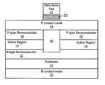
- FIG. 1is a cross-sectional view illustrating semiconductor light emitting devices having a current blocking structure according to some embodiments of the present invention.
- FIGS. 2A and 2Bare cross-sectional views illustrating fabrication of semiconductor devices according to some embodiments of the present invention.
- FIGS. 3 through 11are cross-sectional views of light emitting devices according to further embodiments of the present invention.
- FIGS. 12 and 13are perspective views of light emitting devices according to some embodiments of the present invention.
- first, second, etc.may be used herein to describe various elements, components, regions, layers and/or sections, these elements, components, regions, layers and/or sections should not be limited by these terms. These terms are only used to distinguish one element, component, region, layer or section from another region, layer or section. Thus, a first element, component, region, layer or section discussed below could be termed a second element, component, region, layer or section without departing from the teachings of the present invention.
- relative termssuch as “lower” or “bottom” and “upper” or “top,” may be used herein to describe one element's relationship to another elements as illustrated in the Figures. It will be understood that relative terms are intended to encompass different orientations of the device in addition to the orientation depicted in the Figures. For example, if the device in the Figures is turned over, elements described as being on the “lower” side of other elements would then be oriented on “upper” sides of the other elements. The exemplary term “lower”, can therefore, encompasses both an orientation of “lower” and “upper,” depending of the particular orientation of the figure.
- Embodiments of the present inventionare described herein with reference to cross-section illustrations that are schematic illustrations of idealized embodiments of the present invention. As such, variations from the shapes of the illustrations as a result, for example, of manufacturing techniques and/or tolerances, are to be expected. Thus, embodiments of the present invention should not be construed as limited to the particular shapes of regions illustrated herein but are to include deviations in shapes that result, for example, from manufacturing. For example, an etched region illustrated or described as a rectangle will, typically, have rounded or curved features. Thus, the regions illustrated in the figures are schematic in nature and their shapes are not intended to illustrate the precise shape of a region of a device and are not intended to limit the scope of the present invention.
- references to a structure or feature that is disposed “adjacent” another featuremay have portions that overlap or underlie the adjacent feature.
- LEDs disclosed hereininclude a substrate
- the crystalline epitaxial growth substrate on which the epitaxial layers comprising an LED are grownmay be removed, and the freestanding epitaxial layers may be mounted on a substitute carrier substrate or submount which may have better thermal, electrical, structural and/or optical characteristics than the original substrate.
- the invention described hereinis not limited to structures having crystalline epitaxial growth substrates and may be utilized in connection with structures in which the epitaxial layers have been removed from their original growth substrates and bonded to substitute carrier substrates.
- Some embodiments of the present inventionmay provide for improved efficacy of a light emitting device by reducing and/or preventing current flow in an active region of the device in a region beneath a wire bond pad or other non-transparent structure.
- some embodiments of the present inventionmay provide light emitting devices and methods of fabricating light emitting devices having a current blocking mechanism below the wire bond pad. By reducing and/or preventing current from being injected directly beneath the wire bond pad, the current may be more likely to be converted to photon emission in areas of the device not under the wire bond pad. Thus, there may be a reduced probability of light being absorbed by the wire bond pad.
- an increase in efficiency of a light emitting device according to some embodiments of the present inventionmay be proportional to the size of the wire bond pad.
- Embodiments of the present inventionmay be particularly well suited for use in nitride-based light emitting devices such as Group III-nitride based devices.
- Group III nitriderefers to those semiconducting compounds formed between nitrogen and the elements in Group III of the periodic table, usually aluminum (Al), gallium (Ga), and/or indium (In).
- Alaluminum
- Gagallium
- Inindium
- the termalso refers to ternary and quaternary compounds such as AlGaN and AlInGaN.
- the Group III elementscan combine with nitrogen to form binary (e.g., GaN), ternary (e.g., AlGaN, AlInN), and quaternary (e.g., AlInGaN) compounds. These compounds all have empirical formulas in which one mole of nitrogen is combined with a total of one mole of the Group III elements. Accordingly, formulas such as Al x Ga 1-x N where 0 ⁇ x ⁇ 1 are often used to describe them.
- embodiments of the present inventionare described herein with reference to Group III-nitride based light emitting devices, such as gallium nitride based light emitting devices, certain embodiments of the present invention may be suitable for use in other semiconductor light emitting devices, such as for example, GaAs and/or GaP based devices.
- Light emitting devicesmay include a light emitting diode, laser diode and/or other semiconductor device which includes one or more semiconductor layers, which may include silicon, silicon carbide, gallium nitride and/or other semiconductor materials, a substrate which may include sapphire, silicon, silicon carbide and/or other microelectronic substrates, and one or more contact layers which may include metal and/or other conductive layers.
- semiconductor layerswhich may include silicon, silicon carbide, gallium nitride and/or other semiconductor materials
- a substratewhich may include sapphire, silicon, silicon carbide and/or other microelectronic substrates
- contact layerswhich may include metal and/or other conductive layers.
- ultraviolet, blue and/or green LEDsmay be provided.
- the design and fabrication of semiconductor light emitting devicesare well known to those having skill in the art and need not be described in detail herein.
- light emitting devicesmay include structures such as the gallium nitride-based LED and/or laser structures fabricated on a silicon carbide substrate such as those devices manufactured and sold by Cree, Inc. of Durham, N.C.
- the present inventionmay be suitable for use with LED and/or laser structures that provide active regions such as described in U.S. Pat. Nos.
- the LEDs and/or lasersmay be configured to operate such that light emission occurs through the substrate.
- the substratemay be patterned so as to enhance light output of the devices as is described, for example, in the above-cited U.S. Patent Publication No. US 2002/0123164 A1.
- These structuresmay be modified as described herein to provide blocking structures according to some embodiments of the present invention.
- embodiments of the present inventionmay be utilized with light emitting devices having bond pads of differing shapes or sizes.
- the light emitting devicesmay be on differing substrates, such as silicon carbide, sapphire, gallium nitride, silicon or other substrate suitable substrate for providing Group III-nitride devices.
- the light emitting devicesmay be suitable for subsequent singulation and mounting on a suitable carrier.
- the light emitting devicesmay include, for example, single quantum well, multi-quantum well and/or bulk active region devices.
- Some embodiments of the present inventionmay be used with devices utilizing a tunneling contact on the p-side of the device.
- FIG. 1is a cross-sectional schematic illustration of a light emitting device according to some embodiments of the present invention.
- a substrate 10such as an n-type silicon carbide substrate, has an optional n-type semiconductor layer 12 , such as a gallium nitride based layer, provided thereon.
- the n-type semiconductor layer 12may include multiple layers, for example, buffer layers or the like.
- the n-type semiconductor layer 12is provided as an AlGaN layer, that may be of uniform or gradient composition, and/or a GaN layer.
- the n-type semiconductor layer 12may be doped, for example, with silicon, germanium and/or tellurium.
- the contact 20may be located, for example, in a recess that contacts the n-type semiconductor layer 12 , so as to provide a second contact for the device.
- Other configurationsmay also be utilized.
- An active region 14such as a single or double heterostructure, quantum well, multi-quantum well or other such active region may be provided on the n-type semiconductor layer.
- the term “active region”refers to a region of semiconductor material of a light emitting device, that may be one or more layers and/or portions thereof, where a substantial portion of the photons emitted by the device when in operation are generated by carrier recombination. In some embodiments of the present invention, the active region refers to a region where substantially all of the photons emitted by the device are generated by carrier recombination.
- the p-type semiconductor material layer 16may, for example, be a gallium nitride based layer, such as a GaN layer.
- the p-type semiconductor layer 16includes magnesium doped GaN.
- the p-type semiconductor layer 16may include one or multiple layers and may be of uniform or gradient composition. In some embodiments of the present invention, the p-type semiconductor layer 16 is part of the active region 14 .
- a first contact metal layer 18 of contact metal that provides an ohmic contact to the p-type semiconductor material layer 16is also provided.
- the first contact metal layer 18may function as a current spreading layer.
- the first contact metal layer 18may include Pt, indium-tin-oxide (ITO) or another transparent material that can form an ohmic contact to p-type GaN.
- the first contact metal layer 18is light permeable and in some embodiments is substantially transparent.
- the first contact metal layer 18may be a relatively thin layer of Pt.
- the first contact metal layer 18may be a layer of Pt that is about 15 ⁇ thick.
- An optional reflective layer 23may be provided on the first metal contact layer 18 .
- a wire bond pad 22 or other light absorbing (or otherwise non-transparent) featureis provided on the first contact metal layer 18 .
- the wire bond pad 22is provided on the reflective layer 23 , so that the reflective layer 23 is between the wire bond pad 22 and the p-type semiconductor material layer 16 .
- a current spreading finger 154 AFIG. 13
- a second contact metal layer 20 of contact metal that provides an ohmic contact to the n-type semiconductor materialis also provided.
- the second contact metal layer 20may be provided on a side of the substrate 10 opposite the active region 14 .
- the second contact metal layermay be provided on a portion of the n-type semiconductor material layer 12 , for example, in a recess or at a base of a mesa including the active region.
- an optional back-side implant or additional epitaxial layersmay be provided between the substrate 10 and the second contact metal layer 20 .
- a reduced conductivity region 30is provided in the active region 14 .
- the reduced conductivity region 30may be positioned beneath light absorbing and/or non-transparent features and/or regions of the device.
- the reduced conductivity region 30may be positioned beneath the wire bond pad 22 .
- a reduced conductivity region 30may also be positioned beneath other features of the chip, such as passivation regions along an edge of the chip, current spreading fingers on a surface of the chip, or other features or areas of the chip that may tend to absorb light emitted by the chip.
- the reduced conductivity region 30extends through the active region 14 .
- reduced conductivityrefers to a region with reduced current flow over other portions of the active region.
- the reductionis at least an order of magnitude and in some embodiments, substantially all current flow is blocked in the reduced conductivity region.
- the reduced conductivity region 30extends through the active region 14 .
- the reduced conductivity region 30extends from the first contact metal layer 18 to the active region 14 .
- the reduced conductivity regionextends from the first contact layer 18 into the active region 14 .
- the reduced conductivity regionextends from the first contact layer 18 through the active region 14 .
- the reduced conductivity region 30may have substantially the same shape and/or area as the area of the wire bond pad 22 on the first contact metal layer 18 .
- the reduced conductivity region 30has a slightly larger area than the wire bond pad 22 while in other embodiments of the present invention, the reduced conductivity region 30 has a slightly smaller area than the wire bond pad 22 . In certain embodiments of the present invention, the reduced conductivity region 30 does not absorb light or only absorbs a relatively small amount of light. In some embodiments of the present invention, the reduced conductivity region 30 is an insulating region.
- the reduced conductivity region 30may reduce and/or prevent current flow through the active region 14 in the area beneath the wire bond pad 22 , so that carriers have a tendency to be injected in areas other than the reduced conductivity region 30 .
- the presence of the reduced conductivity region 30may reduce and/or prevent light generation through carrier recombination in this region. While not being bound by a particular theory of operation, this may be the case because the likelihood that a photon generated in the portion of the active region beneath the wire bond pad 22 is absorbed by the wire bond pad 22 may be higher than if the photon is generated in a portion of the active region that is not beneath the wire bond pad 22 .
- the portion of the light generated by the light emitting device that is absorbed by the wire bond pad 22may be reduced. For a given set of operating conditions, this reduction in the amount of light absorbed by the wire bond pad 22 may result in increased light extraction from the light emitting device as compared to a device operating under the same conditions where light is generated in the region beneath the wire bond pad 22 .
- some embodiments of the present inventionprovide a reduced conductivity region 30 that extends into and, in some embodiments, through the active region 14 in the area beneath the wire bond pad 22 . This may reduce the likelihood that carriers may spread and be injected into the active region 14 beneath the wire bond pad 22 and, thereby, result in photon generation in the area beneath the wire bond pad 22 .
- FIGS. 2A and 2Billustrate operations according to some embodiments of the present invention for forming light emitting devices having a reduced conductivity region as illustrated in FIG. 1 .
- the various layers/regions of the light emitting deviceare fabricated. The particular operations in the fabrication of the light emitting device will depend on the structure to be fabricated and are described in the United States Patents and/or Applications incorporated by reference above and/or are well known to those of skill in the art and, therefore, need not be repeated herein.
- FIG. 2Aalso illustrates formation of a mask 40 having a window 42 corresponding to the region where the wire bond pad 22 is to be formed.
- An implantis performed using the mask 40 so as to implant atoms into the active region 14 in the region of the wire bond pad 22 so as to form the reduced conductivity region 30 as seen in FIG. 2B .
- Such an implantmay, for example, be a nitrogen implant.
- implant conditions of 60 keV, 2 ⁇ 10 13 cm ⁇ 3 N 2may produce a non-absorbing and insulating region in Mg doped GaN.
- the particular implant energy and/or atomsmay depend on the structure in which the reduced conductivity region 30 is formed.
- the wire bond pad 22may be formed in the window 42 .
- a reflective layer 23may be formed in the window 42 prior to formation of the wire bond pad 22 .
- the wire bond pad 22 (and possibly the reflective layer 23 ) and the reduced conductivity region 30may be self-aligned.
- the wire bond pad 22may be formed, for example, by forming a layer or layers of metal and then planarizing the layers to provide the wire bond pad 22 .
- the mask 40may subsequently be removed.
- the mask 40may be made of an insulating material, such as SiO 2 and/or AlN, and may remain on the device as, for example, a passivation layer, or be removed.
- FIG. 3illustrates light emitting devices according to further embodiments of the present invention.
- the first contact metal layer 18includes a first portion 55 in contact with the p-type semiconductor material layer 16 that provides an ohmic contact to the p-type semiconductor material layer 16 and a second portion 57 in contact with the p-type semiconductor material layer 16 that does not form an ohmic contact to the p-type semiconductor material layer 16 .
- the term “ohmic contact”refers to a contact with a specific contact resistivity of less than about 10 e-03 ohm-cm 2 and, in some embodiments less than about 10 e-04 ohm-cm 2 .
- a contact that is rectifying or that has a high specific contact resistivityfor example, a specific contact resistivity of greater than about 10 e-03 ohm-cm 2 , is not an ohmic contact as that term is used herein.
- the second portion 57corresponds to the location of the wire bond pad 22 .
- current injection into the p-type semiconductor material layer 16 in the portion 57may be reduced and/or prevented.
- the portion 57 that does not form an ohmic contactmay be provided by damaging the p-type semiconductor layer 16 and/or the first contact metal layer 18 in the region 50 beneath the wire bond pad 22 .
- the quality of the interface between the contact metal and the p-type semiconductor materialmay determine the quality of the resulting ohmic contact.
- the p-type semiconductor material layer 16 in the region 50may be exposed to a high energy plasma, such as Ar, to reduce p-type conductivity before formation of the first contact metal layer 18 .
- the p-type semiconductor material layer 16 and the first contact metal layer 18 in the region 50may be exposed to a high energy plasma to damage the metal/GaN interface after formation of the first contact metal layer 18 .
- the p-type semiconductor material 16 in the region 50may be exposed to a H 2 while protecting the other regions of the p-type semiconductor material layer 16 before formation of the first contact metal layer 18 .
- the p-type semiconductor material 16 in the region 50may be wet or dry etched while protecting the other regions of the p-type semiconductor material layer 16 before formation of the first contact metal layer 18 .
- the p-type semiconductor material layer 16 in the region 50may be exposed to a high energy laser while protecting the other regions of the p-type semiconductor material 16 before formation of the first contact metal layer 18 .
- Such selective damaging of the p-type semiconductor material layer 16 and/or metal layer 18may be provided, for example, using a mask such as described above with reference to FIGS. 2A and 2B and/or by controlling a laser.
- the particular conditions utilizedmay vary depending on the procedure utilized and the composition of the p-type semiconductor material layer 16 and/or the first metal contact layer 18 .
- FIG. 4Aillustrates light emitting devices according to further embodiments of the present invention.
- a Schottky contact 60is provided on the p-type semiconductor material layer 16 and the first contact metal layer 18 ′ formed on the p-type semiconductor material layer 16 and the Schottky contact 60 .
- the wire bond pad 22is provided on the portion of the first contact metal layer 18 ′ on the Schottky contact 60 .
- a rectifying junctionmay be provided in the region below the wire bond pad 22 .
- the rectifying junctionmay be provided, for example, by implanting the p-type semiconductor material layer 16 with n-type ions so as to convert the region 70 beneath the wire bond pad 22 to n-type semiconductor material. Such an implant may, for example, be carried out using a mask such as discussed above with reference to FIGS. 2A and 2B .
- a region of n-type materialcould be formed where the Schottky contact 60 is illustrated in FIG. 4A and the first contact metal 18 ′ could be formed on the region of n-type semiconductor material and the p-type semiconductor material layer 16 .
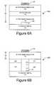
- some embodiments of the inventionprovide a light emitting device 100 A including a substrate 110 on which an n-type semiconductor layer 112 , an active region 114 and a p-type semiconductor layer 116 are formed.
- the semiconductor substrate 110may include a conductive silicon carbide substrate, for example, and the n-type semiconductor layer 112 , the active region 114 and the p-type semiconductor layer 116 may include group III-nitride based semiconductor layers.
- the light emitting device 100 Afurther includes a reduced conductivity region 130 in the p-type semiconductor layer 116 . As seen in FIG.
- the substrate 110may include shaped sidewalls 111 that may increase the efficiency of light extraction from the device 100 A by changing the angle at which light generated in the active region 114 strikes the sidewalls of the device 100 A.
- the reduced conductivity region 130may be located a distance D 1 from the bond pad 122 of about 50 to 400 ⁇ m.
- the reduced conductivity region 130may be formed using any of the methods described above, including implantation of ions into the p-type semiconductor layer 116 .
- the light emitting device 100 Amay be suitable for so-called “flip chip” mounting on an underlying support.
- the semiconductor structuremay be mounted on a submount, bond pad or other surface with the p-type semiconductor layer 116 facing down and the substrate 110 facing up.
- a p-contact metal stack 118is formed on exposed surface of the type semiconductor layer 116 .
- Appropriate metal stacks for flip chip mounting of optoelectronic devicesare disclosed for example in U.S. Patent Publication No. 2003/0015721 entitled “Light Emitting Diodes Including Modifications For Submount Bonding And Manufacturing Methods Therefor,” the disclosure of which is incorporated herein by reference.
- the p-contact metal stack 118may include an ohmic layer 118 A of a metal, such as platinum, that makes an ohmic contact with the p-type semiconductor layer 116 .
- the metal stack 118may further include a reflective layer 118 B, a barrier layer 118 C and/or a bonding layer 118 D.
- the bonding layer 118 Dmay include gold and/or tin, and may be provided to facilitate thermosonic and/or thermocompression bonding of the device 100 A to a submount.
- the reflective layer 118 Bmay include a reflective metal, such as silver or aluminum, and may be provided to reflect light away from a submount and back into the device 100 A so that it may be usefully extracted.
- the barrier layer 118 Cmay include a metal, such as tungsten, titanium, titanium nitride and/or nickel, that may prevent the metal of the bonding layer 118 D from contaminating the ohmic metal 118 A and/or the reflector 118 B. Barrier layers may be formed as described in U.S. Patent Publication No.
- the devicemay include a wire bond pad 122 formed on the substrate 110 .
- An ohmic contact(not shown) may be formed between the wire bond pad 122 and the substrate 110 .
- the ohmic contactmay be formed in self-alignment with the bond pad 122 .
- the reduced conductivity region 130may extend from a surface of the p-type semiconductor layer 116 opposite the active region 114 into the p-type semiconductor layer 116 .
- the reduced conductivity region 130may extend partially and/or completely through the p-type semiconductor layer 116 .
- the reduced conductivity region 130may extend completely through the active region 114 to/into the n-type semiconductor layer 112 .
- the reduced conductivity region 130may be formed using techniques such as those described above with respect to FIGS. 1-4 .
- the reduced conductivity region 130may be formed by implanting ions into the p-type semiconductor layer 116 through a mask, as described above with reference to FIG. 2A .
- the reduced conductivity region 130may be generally aligned with the bond pad 122 . Since the p-type semiconductor layer 116 may be relatively thin compared, for example, to the substrate 110 , and since current may not spread readily in the p-type semiconductor layer 116 , the presence of the reduced conductivity region 130 may reduce the number of photons generated in the device 100 A directly beneath the wire bond pad 122 . Accordingly, the reduced conductivity region 130 may have a shape that is about the same shape as the wire bond pad 122 . Furthermore, the reduced conductivity region 130 may have an area that is about the same as, slightly less than or slightly greater than, the area of the wire bond pad 122 .
- the reduced conductivity regionmay have a diameter that is about 6 to about 30 ⁇ m larger than the diameter of the bond pad 122 .
- bond pad 122may have a diameter of about 100 to 105 ⁇ m
- the reduced conductivity region 130may have a diameter that is about 14 ⁇ m larger than the diameter of the bond pad 122 .
- itmay be desirable to provide a reduced conductivity region 130 that is larger in area than the bond pad 122 .
- the reduced conductivity region 130may also have a circular shape with an area that is less than, about equal to, or slightly greater than the diameter of the wire bond pad 122 .
- FIGS. 6A and 6BFurther embodiments of the invention are shown in FIGS. 6A and 6B in which a light emitting device 100 B is shown including a p-type semiconductor layer 116 an active region 114 and an n-type semiconductor layer 112 .
- a p-contact metal stack 118is formed on a surface of the p-type semiconductor layer 116
- a wire bond pad 122is formed on a surface of the n-type semiconductor layer 112 opposite the p-type semiconductor layer 116 .
- the light emitting device 100 B shown in FIGS. 6A and 6Bmay not include a substrate.
- a reduced conductivity region 130is provided in the p-type semiconductor layer 116 generally aligned with the wire bond pad 122 .
- the reduced conductivity region 130may extend from a surface of the p-type semiconductor layer 116 opposite the active region 114 into the p-type semiconductor layer 116 .
- the reduced conductivity region 130may extend partially and/or completely through the p-type semiconductor layer 116 .
- the reduced conductivity region 130may have an area that is equal to, greater than, or less than the area of the wire bond pad 122 .
- the reduced conductivity region 130may be located within the device 100 B a distance D 2 from the wire bond pad 122 .
- the distance D 2may be from 0.3 to 10 ⁇ m. In particular, the distance D 2 may be about 2 to 3 ⁇ m.
- FIGS. 11A-11Care plan view illustrations of a light emitting device 100 B including a wire bond pad 122 and an aligned reduced conductivity region 130 .
- the reduced conductivity region 130may have a peripheral shape that is similar to the peripheral shape of the wire bond pad 122 , which in the embodiments illustrated in FIGS. 11A-11C is generally circular.
- the wire bond pad 122 and the reduced conductivity region 130may have other peripheral shapes, such as rectangular, star, cross or other shape or combination of shapes.
- the reduced conductivity region 130may have an area that is slightly larger than the area of the wire bond pad 122 in some embodiments, while in other embodiments the reduced conductivity region 130 may have an area that is slightly less than ( FIG. 11B ) or about equal to ( FIG. 11C ) the area of the wire bond pad 122 .
- the reduced conductivity region 130may extend completely through the p-type semiconductor layer 116 and into the active region 114 . In some embodiments, including embodiments that do not include a substrate, the reduced conductivity region 130 may extend completely through the active region 114 to/into the n-type semiconductor layer 112 .
- FIG. 7Aillustrates a light emitting device 100 C that includes a p-type semiconductor layer 116 , an active region 114 and an n-type semiconductor layer 112 .
- a wire bond pad 122is formed on a surface of the n-type semiconductor layer 112 .
- a patterned ohmic contact 118is formed on a surface of the p-type semiconductor layer 116 opposite the n-type semiconductor layer 112 .
- the light emitting device 100 Calso includes a non-ohmic contact 140 on the p-type semiconductor layer 116 opposite the wire bond pad 122 .
- the non-ohmic contact 140may include, for example, a rectifying Schottky contact. The formation of rectifying Schottky contacts on nitride-based semiconductor materials is well known to those skilled in the art.
- the non-ohmic contact 140may include a non-conductive material, such as silicon dioxide.
- the non-ohmic contact 140may have a shape that is about the same as the shape of the wire bond pad 122 .
- the contact 140may have an area that is slightly less than, about equal to, or slightly greater than the area of the wire bond pad 122 . Accordingly, when a voltage is applied across the terminals of the device 100 C, current may not flow from the non-ohmic contact 140 into the p-type semiconductor layer 116 , which may reduce the number of photons generated in the active layer 114 beneath the wire bond pad 122 .
- the metal stack 118may be formed on the surface of the p-type semiconductor layer 116 in regions other than an area of reduced conductivity 150 opposite the wire bond pad 122 . That is, because the metal stack 118 is not formed in the area 150 , a reduced current may flow through the area 150 when the device is energized, which may reduce the number of photons generated in the active layer 114 beneath the wire bond pad 122 .
- a device 100 Eincludes a p-type semiconductor layer 116 , an active region 114 , and an n-type semiconductor layer 112 .
- a p-type contact 118is formed on a surface of the p-type semiconductor layer 116 opposite the n-type semiconductor layer 112 .
- a wire bond pad 122is formed on a surface of the n-type semiconductor layer 112 opposite the p-type semiconductor layer 116 .
- An ohmic contact 154is formed on the same surface of the n-type semiconductor layer 112 as the wire bond pad 122 , and is electrically connected to the wire bond pad 122 .
- the ohmic contact 154may include a transparent material that forms an ohmic contact to the n-type semiconductor layer 112 , such as ITO.
- a reduced conductivity region 152is formed in the n-type semiconductor layer 112 beneath the wire bond pad 122 .
- the reduced conductivity region 152may extend from the surface of the n-type semiconductor layer 112 at least partially into the n-type semiconductor layer 112 . In some embodiments, the reduced conductivity region 152 may extend completely through the n-type semiconductor layer 112 and to/into the active region 114 .
- FIG. 9Aillustrates a device 100 F according to further embodiments of the invention.
- the device 100 Falso includes a p-type semiconductor layer 116 , an active region 114 , and an n-type semiconductor layer 112 .
- a p-type contact 118is formed on a surface of the p-type semiconductor layer 116 opposite the n-type semiconductor layer 112 .
- a wire bond pad 122is formed on a surface of the n-type semiconductor layer 112 opposite the p-type semiconductor layer 116 .
- An ohmic contact 154is formed on the same surface of the n-type semiconductor layer 112 as the wire bond pad 122 .
- a first reduced conductivity region 152is formed in the n-type semiconductor layer 112 beneath the wire bond pad 122 .
- the first reduced conductivity region 152may be aligned with the wire bond pad 122 and may extend from the surface of the n-type semiconductor layer 112 at least partially into the n-type semiconductor layer 112 . In some embodiments, the first reduced conductivity region 152 may extend completely through the n-type semiconductor layer 112 and to/into/through the active region 114 .
- a second reduced conductivity region 150is formed in the p-type semiconductor layer 116 .
- the second reduced conductivity region 150may be aligned with the first reduced conductivity region 152 and/or the wire bond pad 122 .
- the second reduced conductivity region 150may extend from the surface of the p-type semiconductor layer 116 at least partially into the p-type semiconductor layer 116 , and in some cases to/into/through the active region 114 .
- the reduced conductivity regions 150 , 152need not be formed using the same techniques, but could, for example, be formed using different techniques.
- the first reduced conductivity region 152could be formed via ion implantation, while the second reduced conductivity region 150 could be formed using plasma treatment and or exposure to hydrogen gas, or vice-versa.
- one or both of the reduced conductivity regions 150 , 152could be formed by forming a non-ohmic material on the surface of the respective semiconductor layer 116 , 112 prior to forming an electrical contact thereon, or by not forming the ohmic contact on an area of the surface of the semiconductor layer that corresponds to the bond pad 122 .
- FIG. 9Billustrates a device 100 G according to further embodiments of the invention.
- the device 100 Galso includes a p-type semiconductor layer 116 , an active region 114 , and an n-type semiconductor layer 112 .
- a p-type contact 118is formed on a surface of the p-type semiconductor layer 116 opposite the n-type semiconductor layer 112 .
- a wire bond pad 122is formed on a surface of the n-type semiconductor layer 112 opposite the p-type semiconductor layer 116 .
- An ohmic contact 154is formed on the same surface of the n-type semiconductor layer 112 as the wire bond pad 122 .
- a reduced conductivity region 152is formed in the n-type semiconductor layer 112 beneath the wire bond pad 122 .
- the reduced conductivity region 152may be aligned with the wire bond pad 122 and may extend from the surface of the n-type semiconductor layer 112 at least partially into the n-type semiconductor layer 112 . In some embodiments, the reduced conductivity region 152 may extend completely through the n-type semiconductor layer 112 and to/into/through the active region 114 .
- a metal contact 118is formed on a surface of the p-type semiconductor layer 116 opposite the n-type semiconductor layer 112 .
- the metal contact 118forms on ohmic contact to the p-type semiconductor layer 116 in a region other than a reduced conductivity area of the surface of the p-type semiconductor layer 116 that is aligned with the wire bond pad 122 .
- the light emitting device 100 Galso includes a non-ohmic contact 140 on the p-type semiconductor layer 116 opposite the wire bond pad 122 .
- the non-ohmic contact 140may include, for example, a rectifying Schottky contact.
- the non-ohmic contact 140may include a non-conductive material, such as silicon dioxide.
- the non-ohmic contact 140may have a shape that is about the same as the shape of the wire bond pad 122 .
- the contact 140may have an area that is slightly less than, about equal to, or slightly greater than the area of the wire bond pad 122 .
- the non-ohmic contact 140may include a gap on which no contact is formed.
- FIG. 10illustrates a semiconductor light emitting device 100 H that includes a reduced conductivity region 160 that extends beneath the wire bond pad 122 from a surface of the n-type semiconductor layer 112 and through the device 100 G to the opposite surface of the p-type semiconductor layer 116 .
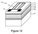
- FIG. 12illustrates a chip structure 100 J including a carrier substrate 210 , such as a silicon substrate, on which an LED structure has been bonded via a metal bonding layer 220 .
- a reflective layer 230is between the bonding layer 220 and the LED structure that includes a p-type semiconductor layer 116 , an active layer 114 and an n-type semiconductor layer 112 .
- a pair of bond pads 122are on the surface of the n-type semiconductor layer 112 opposite the substrate 210 .
- the bond pads 122are electrically connected to a current spreading structure that includes a plurality of current spreading fingers 154 on the n-type semiconductor layer 112 .
- the reduced conductivity region 30may be formed underneath the bond pads 122 , underneath the current spreading fingers 154 , and/or under both the bond pads 122 and the current spreading fingers 154 .
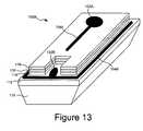
- FIG. 13An exemplary horizontal chip structure 100 K is illustrated in FIG. 13 .
- the chip structure 100 Kincludes a transparent substrate 110 on which an n-type semiconductor layer 112 is formed.
- a mesa structure including an active region 114 and a p-type semiconductor layer 116is on the n-type semiconductor layer.
- a transparent ohmic contact 118which may include ITO, is on the p-type semiconductor layer 116 .
- a bond pad 122 Ais on the transparent ohmic contact layer 118 , and a current spreading finger 154 A extends from the bond pad 122 A.
- a bond pad 122 Bis on the n-type semiconductor layer 112 , and a current spreading finger 154 B extends from the bond pad 122 B.
- a reflective layer 23( FIG. 1 ) may be provided beneath the bond pad 122 A and/or the current spreading finger 154 A.
- the reduced conductivity region 30may be formed underneath the bond pad 122 A, underneath the current spreading fingers 154 A, and/or under both the bond pad 122 A and the current spreading finger 154 A.
- FIGS. 1-13While embodiments of the present invention are illustrated in FIGS. 1-13 with reference to particular light emitting device structures, other structures may be provided according to some embodiments of the present invention. Thus, embodiments of the present invention may be provided by any light emitting structure that includes one or more of the various current blocking mechanisms as described above. For example, current blocking mechanisms according to some embodiments of the present invention may be provided in conjunction with the exemplary light emitting device structures discussed in the United States Patents and/or Applications incorporated by reference above.
- bond padincludes a light absorbing contact structure.
- a bond padmay be a single or multiple layers, may be a metal and/or metal alloy and/or may be of uniform of non-uniform composition.
- the reduced conductivity regions 30may be used to reduce/prevent carrier recombination in areas of a device where generated light may be likely to be absorbed by some feature of the device, such as a bond pad, a current spreading finger, a passivation region, etc. Thus, in some embodiments, the reduced conductivity regions 30 may be aligned with light-absorbing features and/or regions of a device.
- reduced conductivity regions 30may be formed in other areas that are not aligned with light absorbing regions or features of a device. For example, it may be desirable to provide reduced conductivity regions 30 in a device that cause the device to generate light having a desired far-field emission pattern. Thus, in some embodiments, reduced conductivity regions 30 may be used to shape the light emission pattern of a light emitting device.
Landscapes
- Engineering & Computer Science (AREA)
- Computer Hardware Design (AREA)
- Microelectronics & Electronic Packaging (AREA)
- Power Engineering (AREA)
- Led Devices (AREA)
Abstract
Description
Claims (47)
Priority Applications (13)
| Application Number | Priority Date | Filing Date | Title |
|---|---|---|---|
| US11/715,687US7795623B2 (en) | 2004-06-30 | 2007-03-08 | Light emitting devices having current reducing structures and methods of forming light emitting devices having current reducing structures |
| CN200880015255ACN101681961A (en) | 2007-03-08 | 2008-02-19 | Light emitting device with current reducing structure and method of forming light emitting device with current reducing structure |
| JP2009552684AJP5693852B2 (en) | 2007-03-08 | 2008-02-19 | LIGHT EMITTING DEVICE WITH CURRENT REDUCING STRUCTURE AND METHOD FOR FORMING LIGHT EMITTING DEVICE WITH CURRENT REDUCING STRUCTURE |
| EP08725740.8AEP2118938B1 (en) | 2007-03-08 | 2008-02-19 | Light emitting devices having current reducing structures and methods of forming light emitting devices having current reducing structures |
| CN201510512428.9ACN105098012B (en) | 2007-03-08 | 2008-02-19 | Light-emitting device and method of making the same |
| KR1020147007701AKR20140054344A (en) | 2007-03-08 | 2008-02-19 | Light emitting devices having current reducing structures and methods of forming light emitting devices having current reducing structures |
| PCT/US2008/002140WO2008112064A2 (en) | 2007-03-08 | 2008-02-19 | Light emitting devices having current reducing structures and methods of forming light emitting devices having current reducing structures |
| KR1020147019705AKR20140103337A (en) | 2007-03-08 | 2008-02-19 | Light emitting devices having current reducing structures and methods of forming light emitting devices having current reducing structures |
| EP17180805.8AEP3264475B1 (en) | 2007-03-08 | 2008-02-19 | Light emitting devices having current reducing structures |
| KR1020097020887AKR20090117904A (en) | 2007-03-08 | 2008-02-19 | Method of forming light emitting elements having current reducing structures and light emitting elements having current reducing structures |
| US12/879,692US8163577B2 (en) | 2004-06-30 | 2010-09-10 | Methods of forming light emitting devices having current reducing structures |
| US13/406,251US8436368B2 (en) | 2004-06-30 | 2012-02-27 | Methods of forming light emitting devices having current reducing structures |
| US13/856,928US8704240B2 (en) | 2004-06-30 | 2013-04-04 | Light emitting devices having current reducing structures |
Applications Claiming Priority (2)
| Application Number | Priority Date | Filing Date | Title |
|---|---|---|---|
| US10/881,814US20060002442A1 (en) | 2004-06-30 | 2004-06-30 | Light emitting devices having current blocking structures and methods of fabricating light emitting devices having current blocking structures |
| US11/715,687US7795623B2 (en) | 2004-06-30 | 2007-03-08 | Light emitting devices having current reducing structures and methods of forming light emitting devices having current reducing structures |
Related Parent Applications (1)
| Application Number | Title | Priority Date | Filing Date |
|---|---|---|---|
| US10/881,814Continuation-In-PartUS20060002442A1 (en) | 2004-06-30 | 2004-06-30 | Light emitting devices having current blocking structures and methods of fabricating light emitting devices having current blocking structures |
Related Child Applications (1)
| Application Number | Title | Priority Date | Filing Date |
|---|---|---|---|
| US12/879,692DivisionUS8163577B2 (en) | 2004-06-30 | 2010-09-10 | Methods of forming light emitting devices having current reducing structures |
Publications (2)
| Publication Number | Publication Date |
|---|---|
| US20080217635A1 US20080217635A1 (en) | 2008-09-11 |
| US7795623B2true US7795623B2 (en) | 2010-09-14 |
Family
ID=39428041
Family Applications (4)
| Application Number | Title | Priority Date | Filing Date |
|---|---|---|---|
| US11/715,687Active2025-12-01US7795623B2 (en) | 2004-06-30 | 2007-03-08 | Light emitting devices having current reducing structures and methods of forming light emitting devices having current reducing structures |
| US12/879,692Expired - LifetimeUS8163577B2 (en) | 2004-06-30 | 2010-09-10 | Methods of forming light emitting devices having current reducing structures |
| US13/406,251Expired - Fee RelatedUS8436368B2 (en) | 2004-06-30 | 2012-02-27 | Methods of forming light emitting devices having current reducing structures |
| US13/856,928Expired - LifetimeUS8704240B2 (en) | 2004-06-30 | 2013-04-04 | Light emitting devices having current reducing structures |
Family Applications After (3)
| Application Number | Title | Priority Date | Filing Date |
|---|---|---|---|
| US12/879,692Expired - LifetimeUS8163577B2 (en) | 2004-06-30 | 2010-09-10 | Methods of forming light emitting devices having current reducing structures |
| US13/406,251Expired - Fee RelatedUS8436368B2 (en) | 2004-06-30 | 2012-02-27 | Methods of forming light emitting devices having current reducing structures |
| US13/856,928Expired - LifetimeUS8704240B2 (en) | 2004-06-30 | 2013-04-04 | Light emitting devices having current reducing structures |
Country Status (6)
| Country | Link |
|---|---|
| US (4) | US7795623B2 (en) |
| EP (2) | EP2118938B1 (en) |
| JP (1) | JP5693852B2 (en) |
| KR (3) | KR20090117904A (en) |
| CN (2) | CN101681961A (en) |
| WO (1) | WO2008112064A2 (en) |
Cited By (53)
| Publication number | Priority date | Publication date | Assignee | Title |
|---|---|---|---|---|
| US20080111139A1 (en)* | 2006-11-14 | 2008-05-15 | Samsung Electro-Mechanics Company Ltd. | Vertical light emitting device and method of manufacturing the same |
| US20090242929A1 (en)* | 2008-03-31 | 2009-10-01 | Chao-Kun Lin | Light emitting diodes with patterned current blocking metal contact |
| US20090267083A1 (en)* | 2008-04-28 | 2009-10-29 | Jie Cui | Trenched substrate for crystal growth and wafer bonding |
| US20100025719A1 (en)* | 2008-08-01 | 2010-02-04 | Cree, Inc. | Bond pad design for enhancing light extraction from led chips |
| US20100140637A1 (en)* | 2008-12-08 | 2010-06-10 | Matthew Donofrio | Light Emitting Diode with a Dielectric Mirror having a Lateral Configuration |
| US20100276698A1 (en)* | 2009-04-29 | 2010-11-04 | Cree, Inc. | Gate electrodes for millimeter-wave operation and methods of fabrication |
| US20100314649A1 (en)* | 2009-06-10 | 2010-12-16 | Bridgelux, Inc. | Thin-film led with p and n contacts electricall isolated from the substrate |
| US20110050681A1 (en)* | 2009-08-27 | 2011-03-03 | Novatek Microelectronics Corp. | Low voltage differential signal output stage |
| US20110121357A1 (en)* | 2009-11-25 | 2011-05-26 | Steven Lester | LED with Improved Injection Efficiency |
| US20120292631A1 (en)* | 2011-05-16 | 2012-11-22 | Kabushiki Kaisha Toshiba | Semiconductor light emitting device |
| USD672731S1 (en) | 2011-01-24 | 2012-12-18 | Cree, Inc. | Light emitting diode |
| USD675581S1 (en)* | 2011-01-21 | 2013-02-05 | Cree, Inc. | Light emitting diode |
| USD675580S1 (en)* | 2011-02-24 | 2013-02-05 | Cree, Inc. | Light emitting diode |
| USD676981S1 (en) | 2009-10-27 | 2013-02-26 | Cree, Inc. | Hybrid reflector system for a lighting unit |
| US8395165B2 (en) | 2011-07-08 | 2013-03-12 | Bridelux, Inc. | Laterally contacted blue LED with superlattice current spreading layer |
| USD682225S1 (en)* | 2011-01-24 | 2013-05-14 | Cree, Inc. | Light emitting diode |
| US8529102B2 (en) | 2009-04-06 | 2013-09-10 | Cree, Inc. | Reflector system for lighting device |
| US8552465B2 (en) | 2011-11-09 | 2013-10-08 | Toshiba Techno Center Inc. | Method for reducing stress in epitaxial growth |
| US8558247B2 (en) | 2011-09-06 | 2013-10-15 | Toshiba Techno Center Inc. | GaN LEDs with improved area and method for making the same |
| US8556469B2 (en) | 2010-12-06 | 2013-10-15 | Cree, Inc. | High efficiency total internal reflection optic for solid state lighting luminaires |
| US8564010B2 (en) | 2011-08-04 | 2013-10-22 | Toshiba Techno Center Inc. | Distributed current blocking structures for light emitting diodes |
| US8581267B2 (en) | 2011-11-09 | 2013-11-12 | Toshiba Techno Center Inc. | Series connected segmented LED |
| US20130320370A1 (en)* | 2012-05-29 | 2013-12-05 | Micron Technology, Inc. | Solid state transducer dies having reflective features over contacts and associated systems and methods |
| US8624482B2 (en) | 2011-09-01 | 2014-01-07 | Toshiba Techno Center Inc. | Distributed bragg reflector for reflecting light of multiple wavelengths from an LED |
| US8664679B2 (en) | 2011-09-29 | 2014-03-04 | Toshiba Techno Center Inc. | Light emitting devices having light coupling layers with recessed electrodes |
| US8669585B1 (en) | 2011-09-03 | 2014-03-11 | Toshiba Techno Center Inc. | LED that has bounding silicon-doped regions on either side of a strain release layer |
| US8680556B2 (en) | 2011-03-24 | 2014-03-25 | Cree, Inc. | Composite high reflectivity layer |
| US8686430B2 (en) | 2011-09-07 | 2014-04-01 | Toshiba Techno Center Inc. | Buffer layer for GaN-on-Si LED |
| US8686429B2 (en) | 2011-06-24 | 2014-04-01 | Cree, Inc. | LED structure with enhanced mirror reflectivity |
| US8698184B2 (en) | 2011-01-21 | 2014-04-15 | Cree, Inc. | Light emitting diodes with low junction temperature and solid state backlight components including light emitting diodes with low junction temperature |
| US8698163B2 (en) | 2011-09-29 | 2014-04-15 | Toshiba Techno Center Inc. | P-type doping layers for use with light emitting devices |
| US8710536B2 (en) | 2008-12-08 | 2014-04-29 | Cree, Inc. | Composite high reflectivity layer |
| US8764224B2 (en) | 2010-08-12 | 2014-07-01 | Cree, Inc. | Luminaire with distributed LED sources |
| US8853668B2 (en) | 2011-09-29 | 2014-10-07 | Kabushiki Kaisha Toshiba | Light emitting regions for use with light emitting devices |
| US8865565B2 (en) | 2011-08-02 | 2014-10-21 | Kabushiki Kaisha Toshiba | LED having a low defect N-type layer that has grown on a silicon substrate |
| US8896007B2 (en) | 2012-09-12 | 2014-11-25 | High Power Opto, Inc. | Semiconductor light-emitting device and fabricating method thereof |
| US8916906B2 (en) | 2011-07-29 | 2014-12-23 | Kabushiki Kaisha Toshiba | Boron-containing buffer layer for growing gallium nitride on silicon |
| US9012921B2 (en) | 2011-09-29 | 2015-04-21 | Kabushiki Kaisha Toshiba | Light emitting devices having light coupling layers |
| US9012939B2 (en) | 2011-08-02 | 2015-04-21 | Kabushiki Kaisha Toshiba | N-type gallium-nitride layer having multiple conductive intervening layers |
| US9105824B2 (en) | 2010-04-09 | 2015-08-11 | Cree, Inc. | High reflective board or substrate for LEDs |
| US9130068B2 (en) | 2011-09-29 | 2015-09-08 | Manutius Ip, Inc. | Light emitting devices having dislocation density maintaining buffer layers |
| US9142743B2 (en) | 2011-08-02 | 2015-09-22 | Kabushiki Kaisha Toshiba | High temperature gold-free wafer bonding for light emitting diodes |
| US9159869B2 (en) | 2011-08-03 | 2015-10-13 | Kabushiki Kaisha Toshiba | LED on silicon substrate using zinc-sulfide as buffer layer |
| US9178114B2 (en) | 2011-09-29 | 2015-11-03 | Manutius Ip, Inc. | P-type doping layers for use with light emitting devices |
| US9196798B2 (en) | 2012-09-12 | 2015-11-24 | High Power Opto. Inc. | Semiconductor light-emitting device and fabricating method thereof |
| US9343641B2 (en) | 2011-08-02 | 2016-05-17 | Manutius Ip, Inc. | Non-reactive barrier metal for eutectic bonding process |
| US9461201B2 (en) | 2007-11-14 | 2016-10-04 | Cree, Inc. | Light emitting diode dielectric mirror |
| US9543490B2 (en) | 2010-09-24 | 2017-01-10 | Seoul Semiconductor Co., Ltd. | Wafer-level light emitting diode package and method of fabricating the same |
| US9617656B2 (en) | 2011-07-25 | 2017-04-11 | Toshiba Corporation | Nucleation of aluminum nitride on a silicon substrate using an ammonia preflow |
| US9728676B2 (en) | 2011-06-24 | 2017-08-08 | Cree, Inc. | High voltage monolithic LED chip |
| US10186644B2 (en) | 2011-06-24 | 2019-01-22 | Cree, Inc. | Self-aligned floating mirror for contact vias |
| US10580929B2 (en) | 2016-03-30 | 2020-03-03 | Seoul Viosys Co., Ltd. | UV light emitting diode package and light emitting diode module having the same |
| US10658546B2 (en) | 2015-01-21 | 2020-05-19 | Cree, Inc. | High efficiency LEDs and methods of manufacturing |
Families Citing this family (65)
| Publication number | Priority date | Publication date | Assignee | Title |
|---|---|---|---|---|
| TWI294699B (en)* | 2006-01-27 | 2008-03-11 | Epistar Corp | Light emitting device and method of forming the same |
| CA2523544A1 (en) | 2003-04-30 | 2004-11-18 | Cree, Inc. | High powered light emitter packages with compact optics |
| US7534633B2 (en)* | 2004-07-02 | 2009-05-19 | Cree, Inc. | LED with substrate modifications for enhanced light extraction and method of making same |
| US8878245B2 (en)* | 2006-11-30 | 2014-11-04 | Cree, Inc. | Transistors and method for making ohmic contact to transistors |
| US8021904B2 (en)* | 2007-02-01 | 2011-09-20 | Cree, Inc. | Ohmic contacts to nitrogen polarity GaN |
| US9484499B2 (en)* | 2007-04-20 | 2016-11-01 | Cree, Inc. | Transparent ohmic contacts on light emitting diodes with carrier substrates |
| US11114594B2 (en) | 2007-08-24 | 2021-09-07 | Creeled, Inc. | Light emitting device packages using light scattering particles of different size |
| US9634191B2 (en) | 2007-11-14 | 2017-04-25 | Cree, Inc. | Wire bond free wafer level LED |
| US8575633B2 (en) | 2008-12-08 | 2013-11-05 | Cree, Inc. | Light emitting diode with improved light extraction |
| US9660153B2 (en) | 2007-11-14 | 2017-05-23 | Cree, Inc. | Gap engineering for flip-chip mounted horizontal LEDs |
| US8536584B2 (en)* | 2007-11-14 | 2013-09-17 | Cree, Inc. | High voltage wire bond free LEDS |
| US9754926B2 (en) | 2011-01-31 | 2017-09-05 | Cree, Inc. | Light emitting diode (LED) arrays including direct die attach and related assemblies |
| US8368100B2 (en)* | 2007-11-14 | 2013-02-05 | Cree, Inc. | Semiconductor light emitting diodes having reflective structures and methods of fabricating same |
| US9431589B2 (en)* | 2007-12-14 | 2016-08-30 | Cree, Inc. | Textured encapsulant surface in LED packages |
| US8058088B2 (en) | 2008-01-15 | 2011-11-15 | Cree, Inc. | Phosphor coating systems and methods for light emitting structures and packaged light emitting diodes including phosphor coating |
| US8940561B2 (en)* | 2008-01-15 | 2015-01-27 | Cree, Inc. | Systems and methods for application of optical materials to optical elements |
| JP5126884B2 (en)* | 2008-01-16 | 2013-01-23 | シャープ株式会社 | Nitride semiconductor light emitting device and method for manufacturing nitride semiconductor light emitting device |
| US8373152B2 (en)* | 2008-03-27 | 2013-02-12 | Lg Innotek Co., Ltd. | Light-emitting element and a production method therefor |
| EP2280426B1 (en)* | 2008-04-16 | 2017-07-05 | LG Innotek Co., Ltd. | Light-emitting device |
| US8471239B2 (en)* | 2008-04-25 | 2013-06-25 | Lg Innotek Co., Ltd. | Light-emitting element and a production method therefor |
| US8154038B2 (en)* | 2008-07-01 | 2012-04-10 | Taiwan Semiconductor Manufacturing Co., Ltd | Group-III nitride for reducing stress caused by metal nitride reflector |
| KR101047634B1 (en) | 2008-11-24 | 2011-07-07 | 엘지이노텍 주식회사 | Light emitting device and manufacturing method |
| KR101134720B1 (en)* | 2009-02-16 | 2012-04-13 | 엘지이노텍 주식회사 | Semiconductor light emitting device and fabrication method thereof |
| US9093293B2 (en) | 2009-04-06 | 2015-07-28 | Cree, Inc. | High voltage low current surface emitting light emitting diode |
| US8476668B2 (en)* | 2009-04-06 | 2013-07-02 | Cree, Inc. | High voltage low current surface emitting LED |
| KR100999726B1 (en)* | 2009-05-04 | 2010-12-08 | 엘지이노텍 주식회사 | Light emitting device and manufacturing method |
| KR20100122998A (en)* | 2009-05-14 | 2010-11-24 | 엘지이노텍 주식회사 | Light emitting device and method for fabricating the same |
| KR101154750B1 (en)* | 2009-09-10 | 2012-06-08 | 엘지이노텍 주식회사 | Light emitting device and method for fabricating the same |
| TWI398965B (en)* | 2009-11-25 | 2013-06-11 | Formosa Epitaxy Inc | Light emitting diode chip and package structure thereof |
| KR101091304B1 (en)* | 2010-01-20 | 2011-12-07 | 엘지이노텍 주식회사 | Light emitting device package and its manufacturing method |
| KR101014155B1 (en)* | 2010-03-10 | 2011-02-10 | 엘지이노텍 주식회사 | Light emitting device, light emitting device manufacturing method and light emitting device package |
| KR101054984B1 (en)* | 2010-03-26 | 2011-08-05 | 엘지이노텍 주식회사 | Light emitting device, light emitting device manufacturing method and light emitting device package |
| US8263422B2 (en)* | 2010-04-26 | 2012-09-11 | Varian Semiconductor Equipment Associates, Inc. | Bond pad isolation and current confinement in an LED using ion implantation |
| US8154042B2 (en) | 2010-04-29 | 2012-04-10 | Koninklijke Philips Electronics N V | Light emitting device with trenches and a top contact |
| US8329482B2 (en) | 2010-04-30 | 2012-12-11 | Cree, Inc. | White-emitting LED chips and method for making same |
| KR101525913B1 (en)* | 2010-06-22 | 2015-06-10 | 순천대학교 산학협력단 | Verticle light emitting diodes and its fabricating method |
| US8502244B2 (en)* | 2010-08-31 | 2013-08-06 | Micron Technology, Inc. | Solid state lighting devices with current routing and associated methods of manufacturing |
| US8455882B2 (en) | 2010-10-15 | 2013-06-04 | Cree, Inc. | High efficiency LEDs |
| US9053958B2 (en) | 2011-01-31 | 2015-06-09 | Cree, Inc. | Light emitting diode (LED) arrays including direct die attach and related assemblies |
| US9673363B2 (en) | 2011-01-31 | 2017-06-06 | Cree, Inc. | Reflective mounting substrates for flip-chip mounted horizontal LEDs |
| US9508904B2 (en) | 2011-01-31 | 2016-11-29 | Cree, Inc. | Structures and substrates for mounting optical elements and methods and devices for providing the same background |
| US9166126B2 (en) | 2011-01-31 | 2015-10-20 | Cree, Inc. | Conformally coated light emitting devices and methods for providing the same |
| US9831220B2 (en) | 2011-01-31 | 2017-11-28 | Cree, Inc. | Light emitting diode (LED) arrays including direct die attach and related assemblies |
| US9401103B2 (en) | 2011-02-04 | 2016-07-26 | Cree, Inc. | LED-array light source with aspect ratio greater than 1 |
| US9362455B2 (en)* | 2011-02-24 | 2016-06-07 | Cree, Inc. | Semiconductor light emitting diodes having multiple bond pads and current spreading structures |
| JP2012186195A (en)* | 2011-03-03 | 2012-09-27 | Toshiba Corp | Semiconductor light-emitting element and method of manufacturing the same |
| JP5433609B2 (en) | 2011-03-03 | 2014-03-05 | 株式会社東芝 | Semiconductor light emitting device and manufacturing method thereof |
| JP2013093412A (en)* | 2011-10-25 | 2013-05-16 | Showa Denko Kk | Light emitting diode, manufacturing method of light emitting diode, light emitting diode lamp, and lighting device |
| JP2014532993A (en)* | 2011-11-07 | 2014-12-08 | コーニンクレッカ フィリップス エヌ ヴェ | Improved p-type contact with more uniform injection and less optical loss |
| KR101219290B1 (en)* | 2011-11-08 | 2013-01-21 | 순천대학교 산학협력단 | Method for fabricating light emitting diodes |
| US20130214294A1 (en) | 2012-02-17 | 2013-08-22 | Epistar Corporation | Light emitting device with planar current block structure |
| US20130221320A1 (en)* | 2012-02-27 | 2013-08-29 | Tsmc Solid State Lighting Ltd. | Led with embedded doped current blocking layer |
| JP5694215B2 (en)* | 2012-03-07 | 2015-04-01 | 株式会社東芝 | Semiconductor light emitting device |
| KR101929891B1 (en) | 2012-06-08 | 2018-12-17 | 엘지이노텍 주식회사 | Light emitting device, light emitting device package, and light unit |
| CN102779914A (en)* | 2012-08-01 | 2012-11-14 | 厦门市三安光电科技有限公司 | Vertical light-emitting diode with current blocking effect and manufacturing method thereof |
| KR101482526B1 (en)* | 2012-12-28 | 2015-01-16 | 일진엘이디(주) | Method of manufacturing nitride semiconductor light emitting device |
| TWI478387B (en)* | 2013-10-23 | 2015-03-21 | Lextar Electronics Corp | Light-emitting diode structure |
| KR102153123B1 (en)* | 2014-06-10 | 2020-10-26 | 엘지이노텍 주식회사 | Light emitting deviceand light emitting device package thereof |
| US10224457B2 (en) | 2014-11-06 | 2019-03-05 | Lumileds Llc | Light emitting device with trench beneath a top contact |
| CN104409595B (en)* | 2014-12-03 | 2017-05-03 | 佛山市国星半导体技术有限公司 | Vertical light emitting diode (LED) with current blocking structures and manufacturing method thereof |
| USD826871S1 (en) | 2014-12-11 | 2018-08-28 | Cree, Inc. | Light emitting diode device |
| KR102386513B1 (en)* | 2016-08-05 | 2022-04-22 | 서울바이오시스 주식회사 | Light emitting device |
| US10763389B1 (en)* | 2019-06-11 | 2020-09-01 | Facebook Technologies, Llc | LED structure with minimized light emission area |
| US11101418B1 (en) | 2019-09-10 | 2021-08-24 | Facebook Technologies, Llc | Spacer for self-aligned mesa |
| US11164995B2 (en) | 2020-02-20 | 2021-11-02 | Facebook Technologies, Llc | 3-D structure for increasing contact surface area for LEDs |
Citations (53)
| Publication number | Priority date | Publication date | Assignee | Title |
|---|---|---|---|---|
| US4864370A (en) | 1987-11-16 | 1989-09-05 | Motorola, Inc. | Electrical contact for an LED |
| US4918497A (en) | 1988-12-14 | 1990-04-17 | Cree Research, Inc. | Blue light emitting diode formed in silicon carbide |
| US4966862A (en) | 1989-08-28 | 1990-10-30 | Cree Research, Inc. | Method of production of light emitting diodes |
| JPH0389568A (en) | 1989-08-31 | 1991-04-15 | Toshiba Corp | Light emitting diode and manufacture thereof |
| US5027168A (en) | 1988-12-14 | 1991-06-25 | Cree Research, Inc. | Blue light emitting diode formed in silicon carbide |
| US5048035A (en) | 1989-05-31 | 1991-09-10 | Kabushiki Kaisha Toshiba | Semiconductor light emitting device |
| US5210051A (en) | 1990-03-27 | 1993-05-11 | Cree Research, Inc. | High efficiency light emitting diodes from bipolar gallium nitride |
| JPH05235408A (en) | 1992-02-24 | 1993-09-10 | Sharp Corp | Semiconductor light emitting device and manufacturing method thereof |
| US5245622A (en) | 1992-05-07 | 1993-09-14 | Bandgap Technology Corporation | Vertical-cavity surface-emitting lasers with intra-cavity structures |
| US5338944A (en) | 1993-09-22 | 1994-08-16 | Cree Research, Inc. | Blue light-emitting diode with degenerate junction structure |
| GB2280061A (en) | 1993-06-30 | 1995-01-18 | Mitsubishi Chem Ind | Light emitting device |
| US5393993A (en) | 1993-12-13 | 1995-02-28 | Cree Research, Inc. | Buffer structure between silicon carbide and gallium nitride and resulting semiconductor devices |
| DE4338187A1 (en) | 1993-11-09 | 1995-05-11 | Telefunken Microelectron | Light-emitting semiconductor component |
| US5416342A (en) | 1993-06-23 | 1995-05-16 | Cree Research, Inc. | Blue light-emitting diode with high external quantum efficiency |
| US5523589A (en) | 1994-09-20 | 1996-06-04 | Cree Research, Inc. | Vertical geometry light emitting diode with group III nitride active layer and extended lifetime |
| US5604135A (en) | 1994-08-12 | 1997-02-18 | Cree Research, Inc. | Method of forming green light emitting diode in silicon carbide |
| US5631190A (en) | 1994-10-07 | 1997-05-20 | Cree Research, Inc. | Method for producing high efficiency light-emitting diodes and resulting diode structures |
| US5739554A (en) | 1995-05-08 | 1998-04-14 | Cree Research, Inc. | Double heterojunction light emitting diode with gallium nitride active layer |
| US5789768A (en) | 1997-06-23 | 1998-08-04 | Epistar Corporation | Light emitting diode having transparent conductive oxide formed on the contact layer |
| US5793062A (en) | 1995-08-10 | 1998-08-11 | Hewlett-Packard Company | Transparent substrate light emitting diodes with directed light output |
| DE19817368A1 (en) | 1997-04-18 | 1998-12-24 | Epistar Corp | LED with high brightness |
| EP0911887A2 (en) | 1997-10-27 | 1999-04-28 | Matsushita Electric Industrial Co., Ltd. | Light-emitting diode device and method for fabricating the same |
| JPH11186607A (en) | 1997-12-25 | 1999-07-09 | Showa Denko Kk | Compound semiconductor light emitting device |
| EP0929109A1 (en) | 1998-01-08 | 1999-07-14 | Pioneer Electronic Corporation | Method for manufacturing a semiconductor light emitting device |
| JP2000294837A (en) | 1999-04-05 | 2000-10-20 | Stanley Electric Co Ltd | Gallium nitride based compound semiconductor light emitting device |
| US6165809A (en) | 1998-02-10 | 2000-12-26 | Sharp Kabushiki Kaisha | Method of fabricating light emitting diodes |
| US6177688B1 (en) | 1998-11-24 | 2001-01-23 | North Carolina State University | Pendeoepitaxial gallium nitride semiconductor layers on silcon carbide substrates |
| US6187606B1 (en) | 1997-10-07 | 2001-02-13 | Cree, Inc. | Group III nitride photonic devices on silicon carbide substrates with conductive buffer interlayer structure |
| JP2001077414A (en) | 1999-09-07 | 2001-03-23 | Showa Denko Kk | Group iii nitride semiconductor light-emitting diode |
| JP2001085742A (en) | 1999-09-17 | 2001-03-30 | Toshiba Corp | Semiconductor light emitting device and method of manufacturing semiconductor light emitting device |
| US6258614B1 (en) | 1995-01-17 | 2001-07-10 | Lumileds Lighting, U.S., Llc | Method for manufacturing a semiconductor light-emitting device |
| US20010050530A1 (en) | 2000-01-18 | 2001-12-13 | Tetsuroh Murakami | Light emitting diode |
| JP2002064221A (en) | 2000-08-18 | 2002-02-28 | Hitachi Cable Ltd | Light emitting diode |
| US6376269B1 (en) | 1999-02-02 | 2002-04-23 | Agilent Technologies, Inc. | Vertical cavity surface emitting laser (VCSEL) using buried Bragg reflectors and method for producing same |
| US6420732B1 (en) | 2000-06-26 | 2002-07-16 | Luxnet Corporation | Light emitting diode of improved current blocking and light extraction structure |
| US20020123164A1 (en) | 2001-02-01 | 2002-09-05 | Slater David B. | Light emitting diodes including modifications for light extraction and manufacturing methods therefor |
| US6455343B1 (en) | 2000-03-28 | 2002-09-24 | United Epitaxy Company, Ltd. | Method of manufacturing light emitting diode with current blocking structure |
| US20020137243A1 (en) | 2001-03-22 | 2002-09-26 | Nai-Chuan Chen | Method for forming a semiconductor device having a metallic substrate |
| US20020163007A1 (en) | 2001-05-01 | 2002-11-07 | Yukio Matsumoto | Semiconductor light emitting device and method for manufacturing the same |
| US20030006418A1 (en) | 2001-05-30 | 2003-01-09 | Emerson David Todd | Group III nitride based light emitting diode structures with a quantum well and superlattice, group III nitride based quantum well structures and group III nitride based superlattice structures |
| JP2003017748A (en) | 2001-06-27 | 2003-01-17 | Seiwa Electric Mfg Co Ltd | Gallium nitride-based compound semiconductor light emitting element and manufacturing method therefor |
| WO2003058772A2 (en) | 2001-12-28 | 2003-07-17 | Finisar Corporation | Current confinement, capacitance reduction and isolation of vcsels using deep elemental traps |
| WO2003061021A2 (en) | 2001-12-21 | 2003-07-24 | Regents Of The University Of California, The Office Of Technology Transfer | Implantation for current confinement in nitride-based vertical optoelectronics |
| US20030146445A1 (en) | 2002-02-01 | 2003-08-07 | Hen Chang Hsiu | Electrode structure of LED and manufacturing of the same |
| US20040056260A1 (en) | 2002-09-19 | 2004-03-25 | Slater David B. | Phosphor-coated light emitting diodes including tapered sidewalls, and fabrication methods therefor |
| US20040066820A1 (en) | 2000-11-28 | 2004-04-08 | Johnson Ralph H. | Versatile method and system for single mode VCSELs |
| JP2004172189A (en) | 2002-11-18 | 2004-06-17 | Shiro Sakai | Nitride semiconductor device and its manufacturing method |
| US20050082558A1 (en) | 2003-10-17 | 2005-04-21 | Atomic Energy Council - Institute Of Nuclear Energy Research | Light-emitting device with a current blocking structure and method for making the same |
| US6919585B2 (en) | 2002-05-17 | 2005-07-19 | Lumei Optoelectronics, Inc. | Light-emitting diode with silicon carbide substrate |
| US6933169B2 (en) | 1995-03-13 | 2005-08-23 | Toyoda Gosei Co., Ltd. | Optical semiconductor device |
| WO2005117147A1 (en) | 2004-05-28 | 2005-12-08 | Osram Opto Semiconductors Gmbh | Method for producing an area having reduced electrical conductivity within a semiconductor layer and optoelectronic semiconductor element |
| US20060002442A1 (en) | 2004-06-30 | 2006-01-05 | Kevin Haberern | Light emitting devices having current blocking structures and methods of fabricating light emitting devices having current blocking structures |
| US20060163586A1 (en) | 2005-01-24 | 2006-07-27 | Cree, Inc. | LED with current confinement structure and surface roughening |
Family Cites Families (72)
| Publication number | Priority date | Publication date | Assignee | Title |
|---|---|---|---|---|
| US4866005A (en)* | 1987-10-26 | 1989-09-12 | North Carolina State University | Sublimation of silicon carbide to produce large, device quality single crystals of silicon carbide |
| JPH0682862B2 (en)* | 1988-01-29 | 1994-10-19 | 日立電線株式会社 | Light emitting diode |
| JPH0278280A (en) | 1988-09-14 | 1990-03-19 | Ricoh Co Ltd | Semiconductor light emitting device |
| US5153889A (en)* | 1989-05-31 | 1992-10-06 | Kabushiki Kaisha Toshiba | Semiconductor light emitting device |
| US4946547A (en)* | 1989-10-13 | 1990-08-07 | Cree Research, Inc. | Method of preparing silicon carbide surfaces for crystal growth |
| US5200022A (en)* | 1990-10-03 | 1993-04-06 | Cree Research, Inc. | Method of improving mechanically prepared substrate surfaces of alpha silicon carbide for deposition of beta silicon carbide thereon and resulting product |
| JPH04264781A (en)* | 1991-02-20 | 1992-09-21 | Eastman Kodak Japan Kk | light emitting diode array |
| JP2798545B2 (en)* | 1992-03-03 | 1998-09-17 | シャープ株式会社 | Semiconductor light emitting device and method of manufacturing the same |
| DE4305296C3 (en)* | 1993-02-20 | 1999-07-15 | Vishay Semiconductor Gmbh | Method of manufacturing a radiation emitting diode |
| JPH0794778A (en)* | 1993-09-22 | 1995-04-07 | Olympus Optical Co Ltd | Light emitting device |
| JP3316062B2 (en)* | 1993-12-09 | 2002-08-19 | 株式会社東芝 | Semiconductor light emitting device |
| US5814839A (en)* | 1995-02-16 | 1998-09-29 | Sharp Kabushiki Kaisha | Semiconductor light-emitting device having a current adjusting layer and a uneven shape light emitting region, and method for producing same |
| US5565694A (en)* | 1995-07-10 | 1996-10-15 | Huang; Kuo-Hsin | Light emitting diode with current blocking layer |
| US5719891A (en)* | 1995-12-18 | 1998-02-17 | Picolight Incorporated | Conductive element with lateral oxidation barrier |
| US5779924A (en)* | 1996-03-22 | 1998-07-14 | Hewlett-Packard Company | Ordered interface texturing for a light emitting device |
| JPH10294531A (en)* | 1997-02-21 | 1998-11-04 | Toshiba Corp | Nitride compound semiconductor light emitting device |
| US6420735B2 (en)* | 1997-05-07 | 2002-07-16 | Samsung Electronics Co., Ltd. | Surface-emitting light-emitting diode |
| DE19745723A1 (en) | 1997-10-16 | 1998-12-10 | Telefunken Microelectron | Light emitting semiconductor device especially LED |
| EP1928034A3 (en)* | 1997-12-15 | 2008-06-18 | Philips Lumileds Lighting Company LLC | Light emitting device |
| US6291839B1 (en)* | 1998-09-11 | 2001-09-18 | Lulileds Lighting, U.S. Llc | Light emitting device having a finely-patterned reflective contact |
| JP2000261029A (en) | 1999-03-12 | 2000-09-22 | Oki Electric Ind Co Ltd | Optical semiconductor element |
| US6222207B1 (en)* | 1999-05-24 | 2001-04-24 | Lumileds Lighting, U.S. Llc | Diffusion barrier for increased mirror reflectivity in reflective solderable contacts on high power LED chip |
| TW437104B (en)* | 1999-05-25 | 2001-05-28 | Wang Tien Yang | Semiconductor light-emitting device and method for manufacturing the same |
| US6287947B1 (en)* | 1999-06-08 | 2001-09-11 | Lumileds Lighting, U.S. Llc | Method of forming transparent contacts to a p-type GaN layer |
| US6133589A (en)* | 1999-06-08 | 2000-10-17 | Lumileds Lighting, U.S., Llc | AlGaInN-based LED having thick epitaxial layer for improved light extraction |
| US6534798B1 (en)* | 1999-09-08 | 2003-03-18 | California Institute Of Technology | Surface plasmon enhanced light emitting diode and method of operation for the same |
| JP2001111103A (en)* | 1999-10-14 | 2001-04-20 | Korai Kagi Kofun Yugenkoshi | Region current density controllable led |
| US6812502B1 (en)* | 1999-11-04 | 2004-11-02 | Uni Light Technology Incorporation | Flip-chip light-emitting device |
| US6492661B1 (en)* | 1999-11-04 | 2002-12-10 | Fen-Ren Chien | Light emitting semiconductor device having reflection layer structure |
| US6410942B1 (en)* | 1999-12-03 | 2002-06-25 | Cree Lighting Company | Enhanced light extraction through the use of micro-LED arrays |
| KR100700993B1 (en)* | 1999-12-03 | 2007-03-30 | 크리, 인코포레이티드 | Light emitting diode having improved light extraction structure and manufacturing method thereof |
| US6514782B1 (en)* | 1999-12-22 | 2003-02-04 | Lumileds Lighting, U.S., Llc | Method of making a III-nitride light-emitting device with increased light generating capability |
| US6992334B1 (en)* | 1999-12-22 | 2006-01-31 | Lumileds Lighting U.S., Llc | Multi-layer highly reflective ohmic contacts for semiconductor devices |
| US6486499B1 (en)* | 1999-12-22 | 2002-11-26 | Lumileds Lighting U.S., Llc | III-nitride light-emitting device with increased light generating capability |
| JP3975388B2 (en) | 2000-04-07 | 2007-09-12 | サンケン電気株式会社 | Semiconductor light emitting device |
| EP2270875B1 (en) | 2000-04-26 | 2018-01-10 | OSRAM Opto Semiconductors GmbH | Sermiconductor light emitting device and method of manufacturing the same |
| JP2002026386A (en)* | 2000-07-10 | 2002-01-25 | Toyoda Gosei Co Ltd | Group III nitride compound semiconductor light emitting device |
| TW461124B (en) | 2000-11-14 | 2001-10-21 | Advanced Epitaxy Technology In | Light emitting diode device with high light transmittance |
| JP4058590B2 (en) | 2001-06-29 | 2008-03-12 | サンケン電気株式会社 | Semiconductor light emitting device |
| US7501023B2 (en)* | 2001-07-06 | 2009-03-10 | Technologies And Devices, International, Inc. | Method and apparatus for fabricating crack-free Group III nitride semiconductor materials |
| US6740906B2 (en)* | 2001-07-23 | 2004-05-25 | Cree, Inc. | Light emitting diodes including modifications for submount bonding |
| US7211833B2 (en) | 2001-07-23 | 2007-05-01 | Cree, Inc. | Light emitting diodes including barrier layers/sublayers |
| JP4055503B2 (en) | 2001-07-24 | 2008-03-05 | 日亜化学工業株式会社 | Semiconductor light emitting device |
| JP2003037285A (en) | 2001-07-25 | 2003-02-07 | Hitachi Cable Ltd | Light emitting diode |
| JP2003168823A (en)* | 2001-09-18 | 2003-06-13 | Toyoda Gosei Co Ltd | Group III nitride compound semiconductor light emitting device |
| JP4089194B2 (en) | 2001-09-28 | 2008-05-28 | 日亜化学工業株式会社 | Nitride semiconductor light emitting diode |
| US7148520B2 (en)* | 2001-10-26 | 2006-12-12 | Lg Electronics Inc. | Diode having vertical structure and method of manufacturing the same |
| TWI276230B (en) | 2001-12-04 | 2007-03-11 | Epitech Corp Ltd | Structure and manufacturing method of light emitting diode |
| US6784462B2 (en)* | 2001-12-13 | 2004-08-31 | Rensselaer Polytechnic Institute | Light-emitting diode with planar omni-directional reflector |
| TW513820B (en) | 2001-12-26 | 2002-12-11 | United Epitaxy Co Ltd | Light emitting diode and its manufacturing method |
| WO2003065464A1 (en)* | 2002-01-28 | 2003-08-07 | Nichia Corporation | Nitride semiconductor device having support substrate and its manufacturing method |
| JP3975763B2 (en)* | 2002-01-30 | 2007-09-12 | 昭和電工株式会社 | Boron phosphide-based semiconductor light-emitting device, manufacturing method thereof, and light-emitting diode |
| US6828596B2 (en)* | 2002-06-13 | 2004-12-07 | Lumileds Lighting U.S., Llc | Contacting scheme for large and small area semiconductor light emitting flip chip devices |
| JP2004047760A (en) | 2002-07-12 | 2004-02-12 | Hitachi Cable Ltd | Epitaxial wafer for light emitting diode and light emitting diode |
| CA2492249A1 (en)* | 2002-07-22 | 2004-01-29 | Cree, Inc. | Light emitting diode including barrier layers and manufacturing methods therefor |
| JP2004165436A (en) | 2002-11-13 | 2004-06-10 | Rohm Co Ltd | Method of manufacturing semiconductor light emitting device |
| TW200409378A (en) | 2002-11-25 | 2004-06-01 | Super Nova Optoelectronics Corp | GaN-based light-emitting diode and the manufacturing method thereof |
| JP4159865B2 (en) | 2002-12-11 | 2008-10-01 | シャープ株式会社 | Nitride compound semiconductor light emitting device manufacturing method |
| JP3720341B2 (en)* | 2003-02-12 | 2005-11-24 | ローム株式会社 | Semiconductor light emitting device |
| US6831302B2 (en)* | 2003-04-15 | 2004-12-14 | Luminus Devices, Inc. | Light emitting devices with improved extraction efficiency |
| JP2005005557A (en) | 2003-06-13 | 2005-01-06 | Hitachi Cable Ltd | Manufacturing method of semiconductor light emitting device |
| JP2003347586A (en) | 2003-07-08 | 2003-12-05 | Toshiba Corp | Semiconductor light-emitting device |
| JP4191566B2 (en)* | 2003-09-12 | 2008-12-03 | アトミック エナジー カウンセル − インスティトゥート オブ ニュークリアー エナジー リサーチ | LIGHT EMITTING DIODE HAVING CURRENT BLOCK STRUCTURE AND METHOD FOR MANUFACTURING THE SAME |
| JP2004096130A (en) | 2003-12-01 | 2004-03-25 | Showa Denko Kk | Nitride semiconductor light emitting diode |
| US20050169336A1 (en)* | 2004-02-04 | 2005-08-04 | Fuji Xerox Co., Ltd. | Vertical-cavity surface-emitting semiconductor laser |
| TWM255518U (en)* | 2004-04-23 | 2005-01-11 | Super Nova Optoelectronics Cor | Vertical electrode structure of Gallium Nitride based LED |
| JP2006066518A (en)* | 2004-08-25 | 2006-03-09 | Sharp Corp | Semiconductor light emitting device and method for manufacturing semiconductor light emitting device |
| KR100533645B1 (en)* | 2004-09-13 | 2005-12-06 | 삼성전기주식회사 | Light emitting diode improved in luminous efficiency |
| US8174037B2 (en)* | 2004-09-22 | 2012-05-08 | Cree, Inc. | High efficiency group III nitride LED with lenticular surface |
| KR100691177B1 (en)* | 2005-05-31 | 2007-03-09 | 삼성전기주식회사 | White light emitting device |
| JP2007123517A (en)* | 2005-10-27 | 2007-05-17 | Toshiba Corp | Semiconductor light emitting device and semiconductor light emitting device |
| CN101315959A (en)* | 2007-06-01 | 2008-12-03 | 富士迈半导体精密工业(上海)有限公司 | High Brightness Light Emitting Diodes |
- 2007
- 2007-03-08USUS11/715,687patent/US7795623B2/enactiveActive
- 2008
- 2008-02-19JPJP2009552684Apatent/JP5693852B2/enactiveActive
- 2008-02-19EPEP08725740.8Apatent/EP2118938B1/enactiveActive
- 2008-02-19EPEP17180805.8Apatent/EP3264475B1/enactiveActive
- 2008-02-19KRKR1020097020887Apatent/KR20090117904A/ennot_activeCeased
- 2008-02-19KRKR1020147019705Apatent/KR20140103337A/ennot_activeCeased
- 2008-02-19CNCN200880015255Apatent/CN101681961A/enactivePending
- 2008-02-19KRKR1020147007701Apatent/KR20140054344A/ennot_activeCeased
- 2008-02-19WOPCT/US2008/002140patent/WO2008112064A2/enactiveApplication Filing
- 2008-02-19CNCN201510512428.9Apatent/CN105098012B/enactiveActive
- 2010
- 2010-09-10USUS12/879,692patent/US8163577B2/ennot_activeExpired - Lifetime
- 2012
- 2012-02-27USUS13/406,251patent/US8436368B2/ennot_activeExpired - Fee Related
- 2013
- 2013-04-04USUS13/856,928patent/US8704240B2/ennot_activeExpired - Lifetime
Patent Citations (63)
| Publication number | Priority date | Publication date | Assignee | Title |
|---|---|---|---|---|
| US4864370A (en) | 1987-11-16 | 1989-09-05 | Motorola, Inc. | Electrical contact for an LED |
| US4918497A (en) | 1988-12-14 | 1990-04-17 | Cree Research, Inc. | Blue light emitting diode formed in silicon carbide |
| US5027168A (en) | 1988-12-14 | 1991-06-25 | Cree Research, Inc. | Blue light emitting diode formed in silicon carbide |
| US5048035A (en) | 1989-05-31 | 1991-09-10 | Kabushiki Kaisha Toshiba | Semiconductor light emitting device |
| US4966862A (en) | 1989-08-28 | 1990-10-30 | Cree Research, Inc. | Method of production of light emitting diodes |
| JPH0389568A (en) | 1989-08-31 | 1991-04-15 | Toshiba Corp | Light emitting diode and manufacture thereof |
| US5210051A (en) | 1990-03-27 | 1993-05-11 | Cree Research, Inc. | High efficiency light emitting diodes from bipolar gallium nitride |
| JPH05235408A (en) | 1992-02-24 | 1993-09-10 | Sharp Corp | Semiconductor light emitting device and manufacturing method thereof |
| US5245622A (en) | 1992-05-07 | 1993-09-14 | Bandgap Technology Corporation | Vertical-cavity surface-emitting lasers with intra-cavity structures |
| US5416342A (en) | 1993-06-23 | 1995-05-16 | Cree Research, Inc. | Blue light-emitting diode with high external quantum efficiency |
| GB2280061A (en) | 1993-06-30 | 1995-01-18 | Mitsubishi Chem Ind | Light emitting device |
| US5338944A (en) | 1993-09-22 | 1994-08-16 | Cree Research, Inc. | Blue light-emitting diode with degenerate junction structure |
| DE4338187A1 (en) | 1993-11-09 | 1995-05-11 | Telefunken Microelectron | Light-emitting semiconductor component |
| US5393993A (en) | 1993-12-13 | 1995-02-28 | Cree Research, Inc. | Buffer structure between silicon carbide and gallium nitride and resulting semiconductor devices |
| US5604135A (en) | 1994-08-12 | 1997-02-18 | Cree Research, Inc. | Method of forming green light emitting diode in silicon carbide |
| US5523589A (en) | 1994-09-20 | 1996-06-04 | Cree Research, Inc. | Vertical geometry light emitting diode with group III nitride active layer and extended lifetime |
| US5912477A (en) | 1994-10-07 | 1999-06-15 | Cree Research, Inc. | High efficiency light emitting diodes |
| US5631190A (en) | 1994-10-07 | 1997-05-20 | Cree Research, Inc. | Method for producing high efficiency light-emitting diodes and resulting diode structures |
| US6258614B1 (en) | 1995-01-17 | 2001-07-10 | Lumileds Lighting, U.S., Llc | Method for manufacturing a semiconductor light-emitting device |
| US6933169B2 (en) | 1995-03-13 | 2005-08-23 | Toyoda Gosei Co., Ltd. | Optical semiconductor device |
| US5739554A (en) | 1995-05-08 | 1998-04-14 | Cree Research, Inc. | Double heterojunction light emitting diode with gallium nitride active layer |
| US6120600A (en) | 1995-05-08 | 2000-09-19 | Cree, Inc. | Double heterojunction light emitting diode with gallium nitride active layer |
| US5793062A (en) | 1995-08-10 | 1998-08-11 | Hewlett-Packard Company | Transparent substrate light emitting diodes with directed light output |
| DE19817368A1 (en) | 1997-04-18 | 1998-12-24 | Epistar Corp | LED with high brightness |
| US6057562A (en) | 1997-04-18 | 2000-05-02 | Epistar Corp. | High efficiency light emitting diode with distributed Bragg reflector |
| US5789768A (en) | 1997-06-23 | 1998-08-04 | Epistar Corporation | Light emitting diode having transparent conductive oxide formed on the contact layer |
| US6201262B1 (en) | 1997-10-07 | 2001-03-13 | Cree, Inc. | Group III nitride photonic devices on silicon carbide substrates with conductive buffer interlay structure |
| US6187606B1 (en) | 1997-10-07 | 2001-02-13 | Cree, Inc. | Group III nitride photonic devices on silicon carbide substrates with conductive buffer interlayer structure |
| EP0911887A2 (en) | 1997-10-27 | 1999-04-28 | Matsushita Electric Industrial Co., Ltd. | Light-emitting diode device and method for fabricating the same |
| JPH11186607A (en) | 1997-12-25 | 1999-07-09 | Showa Denko Kk | Compound semiconductor light emitting device |
| EP0929109A1 (en) | 1998-01-08 | 1999-07-14 | Pioneer Electronic Corporation | Method for manufacturing a semiconductor light emitting device |
| US6165809A (en) | 1998-02-10 | 2000-12-26 | Sharp Kabushiki Kaisha | Method of fabricating light emitting diodes |
| US6177688B1 (en) | 1998-11-24 | 2001-01-23 | North Carolina State University | Pendeoepitaxial gallium nitride semiconductor layers on silcon carbide substrates |
| US6376269B1 (en) | 1999-02-02 | 2002-04-23 | Agilent Technologies, Inc. | Vertical cavity surface emitting laser (VCSEL) using buried Bragg reflectors and method for producing same |
| JP2000294837A (en) | 1999-04-05 | 2000-10-20 | Stanley Electric Co Ltd | Gallium nitride based compound semiconductor light emitting device |
| JP2001077414A (en) | 1999-09-07 | 2001-03-23 | Showa Denko Kk | Group iii nitride semiconductor light-emitting diode |
| JP2001085742A (en) | 1999-09-17 | 2001-03-30 | Toshiba Corp | Semiconductor light emitting device and method of manufacturing semiconductor light emitting device |
| US20040016934A1 (en) | 2000-01-18 | 2004-01-29 | Tetsuroh Murakami | Light emitting diode |
| US20010050530A1 (en) | 2000-01-18 | 2001-12-13 | Tetsuroh Murakami | Light emitting diode |
| US6455343B1 (en) | 2000-03-28 | 2002-09-24 | United Epitaxy Company, Ltd. | Method of manufacturing light emitting diode with current blocking structure |
| US6420732B1 (en) | 2000-06-26 | 2002-07-16 | Luxnet Corporation | Light emitting diode of improved current blocking and light extraction structure |
| JP2002064221A (en) | 2000-08-18 | 2002-02-28 | Hitachi Cable Ltd | Light emitting diode |
| US20040066820A1 (en) | 2000-11-28 | 2004-04-08 | Johnson Ralph H. | Versatile method and system for single mode VCSELs |
| US20020123164A1 (en) | 2001-02-01 | 2002-09-05 | Slater David B. | Light emitting diodes including modifications for light extraction and manufacturing methods therefor |
| US20020137243A1 (en) | 2001-03-22 | 2002-09-26 | Nai-Chuan Chen | Method for forming a semiconductor device having a metallic substrate |
| US20020163007A1 (en) | 2001-05-01 | 2002-11-07 | Yukio Matsumoto | Semiconductor light emitting device and method for manufacturing the same |
| US20030006418A1 (en) | 2001-05-30 | 2003-01-09 | Emerson David Todd | Group III nitride based light emitting diode structures with a quantum well and superlattice, group III nitride based quantum well structures and group III nitride based superlattice structures |
| JP2003017748A (en) | 2001-06-27 | 2003-01-17 | Seiwa Electric Mfg Co Ltd | Gallium nitride-based compound semiconductor light emitting element and manufacturing method therefor |
| WO2003061021A2 (en) | 2001-12-21 | 2003-07-24 | Regents Of The University Of California, The Office Of Technology Transfer | Implantation for current confinement in nitride-based vertical optoelectronics |
| US20030180980A1 (en) | 2001-12-21 | 2003-09-25 | Tal Margalith | Implantation for current confinement in nitride-based vertical optoelectronics |
| WO2003061021A3 (en) | 2001-12-21 | 2004-04-15 | Univ California The Office Of | Implantation for current confinement in nitride-based vertical optoelectronics |
| WO2003058772A2 (en) | 2001-12-28 | 2003-07-17 | Finisar Corporation | Current confinement, capacitance reduction and isolation of vcsels using deep elemental traps |
| WO2003058772A3 (en) | 2001-12-28 | 2004-02-26 | Honeywell Int Inc | Current confinement, capacitance reduction and isolation of vcsels using deep elemental traps |
| US20030146445A1 (en) | 2002-02-01 | 2003-08-07 | Hen Chang Hsiu | Electrode structure of LED and manufacturing of the same |
| US6919585B2 (en) | 2002-05-17 | 2005-07-19 | Lumei Optoelectronics, Inc. | Light-emitting diode with silicon carbide substrate |
| US20040056260A1 (en) | 2002-09-19 | 2004-03-25 | Slater David B. | Phosphor-coated light emitting diodes including tapered sidewalls, and fabrication methods therefor |
| US6853010B2 (en) | 2002-09-19 | 2005-02-08 | Cree, Inc. | Phosphor-coated light emitting diodes including tapered sidewalls, and fabrication methods therefor |
| JP2004172189A (en) | 2002-11-18 | 2004-06-17 | Shiro Sakai | Nitride semiconductor device and its manufacturing method |
| US20050082558A1 (en) | 2003-10-17 | 2005-04-21 | Atomic Energy Council - Institute Of Nuclear Energy Research | Light-emitting device with a current blocking structure and method for making the same |
| US7009214B2 (en)* | 2003-10-17 | 2006-03-07 | Atomic Energy Council —Institute of Nuclear Energy Research | Light-emitting device with a current blocking structure and method for making the same |
| WO2005117147A1 (en) | 2004-05-28 | 2005-12-08 | Osram Opto Semiconductors Gmbh | Method for producing an area having reduced electrical conductivity within a semiconductor layer and optoelectronic semiconductor element |
| US20060002442A1 (en) | 2004-06-30 | 2006-01-05 | Kevin Haberern | Light emitting devices having current blocking structures and methods of fabricating light emitting devices having current blocking structures |
| US20060163586A1 (en) | 2005-01-24 | 2006-07-27 | Cree, Inc. | LED with current confinement structure and surface roughening |
Non-Patent Citations (7)
| Title |
|---|
| Invitation to Pay Additional Fees and, Where Applicable, Protest Fee corresponding to International Application No. PCT/US2008/002140, Mailed Jul. 4, 2008 (8 Pages). |
| Invitation to Pay Additional Fees, Annex to Form PCT/ISA/206-Communication Relating to the Results of the Partial International Search, PCT/US2005/010868, May 3, 2006. |
| Lee et al. "Characteristics of Top-Surface-Emitting GaAs Quantum-Well Lasers" IEEE Photonics Technology Letters 2(9):686-688 (1990). |
| Margalith et al. "Ion Implantation for Current Confinement in InGaN-based RCLEDs," 4th International Symposium on Blue Laser and Light Emitting Diodes, Mar. 2002. |
| Notification of Transmittal of the International Search Report and the Written Opinion of the International Searching Authority, or the Declaration, International Search Report and Written Opinion of the International Searching Authority, PCT Application No. PCT/US2008/002140, Dec. 16, 2008. |
| Notification of Transmittal of the International Search Report and the Written Opinion of the International Searching Authority, or the Declaration, International Search Report, Written Opinion of the International Searching Authority, PCT/US2005/010868, Aug. 17, 2006. |
| Yoo et al. "Fabrication of Vertical-Cavity Front-Surface-Emitting Laser Diode (FSELD) Using a Heterojunction Bipolar Transistor Process" Japanese Journal of Applied Physics 30(3B):L492-L494 (1991. |
Cited By (91)
| Publication number | Priority date | Publication date | Assignee | Title |
|---|---|---|---|---|
| US20080111139A1 (en)* | 2006-11-14 | 2008-05-15 | Samsung Electro-Mechanics Company Ltd. | Vertical light emitting device and method of manufacturing the same |
| US9461201B2 (en) | 2007-11-14 | 2016-10-04 | Cree, Inc. | Light emitting diode dielectric mirror |
| US20090242929A1 (en)* | 2008-03-31 | 2009-10-01 | Chao-Kun Lin | Light emitting diodes with patterned current blocking metal contact |
| US20090267083A1 (en)* | 2008-04-28 | 2009-10-29 | Jie Cui | Trenched substrate for crystal growth and wafer bonding |
| US8664747B2 (en) | 2008-04-28 | 2014-03-04 | Toshiba Techno Center Inc. | Trenched substrate for crystal growth and wafer bonding |
| US20100025719A1 (en)* | 2008-08-01 | 2010-02-04 | Cree, Inc. | Bond pad design for enhancing light extraction from led chips |
| US8384115B2 (en) | 2008-08-01 | 2013-02-26 | Cree, Inc. | Bond pad design for enhancing light extraction from LED chips |
| US20100140637A1 (en)* | 2008-12-08 | 2010-06-10 | Matthew Donofrio | Light Emitting Diode with a Dielectric Mirror having a Lateral Configuration |
| US8017963B2 (en) | 2008-12-08 | 2011-09-13 | Cree, Inc. | Light emitting diode with a dielectric mirror having a lateral configuration |
| US8710536B2 (en) | 2008-12-08 | 2014-04-29 | Cree, Inc. | Composite high reflectivity layer |
| US8529102B2 (en) | 2009-04-06 | 2013-09-10 | Cree, Inc. | Reflector system for lighting device |
| US8741715B2 (en) | 2009-04-29 | 2014-06-03 | Cree, Inc. | Gate electrodes for millimeter-wave operation and methods of fabrication |
| US20100276698A1 (en)* | 2009-04-29 | 2010-11-04 | Cree, Inc. | Gate electrodes for millimeter-wave operation and methods of fabrication |
| US20100314649A1 (en)* | 2009-06-10 | 2010-12-16 | Bridgelux, Inc. | Thin-film led with p and n contacts electricall isolated from the substrate |
| US9142742B2 (en) | 2009-06-10 | 2015-09-22 | Kabushiki Kaisha Toshiba | Thin-film LED with P and N contacts electrically isolated from the substrate |
| US8546832B2 (en) | 2009-06-10 | 2013-10-01 | Toshiba Techno Center Inc. | Thin-film LED with p and n contacts electrically isolated from the substrate |
| US20110050681A1 (en)* | 2009-08-27 | 2011-03-03 | Novatek Microelectronics Corp. | Low voltage differential signal output stage |
| USD676981S1 (en) | 2009-10-27 | 2013-02-26 | Cree, Inc. | Hybrid reflector system for a lighting unit |
| US8525221B2 (en) | 2009-11-25 | 2013-09-03 | Toshiba Techno Center, Inc. | LED with improved injection efficiency |
| US8684749B2 (en) | 2009-11-25 | 2014-04-01 | Toshiba Techno Center Inc. | LED with improved injection efficiency |
| US20110121357A1 (en)* | 2009-11-25 | 2011-05-26 | Steven Lester | LED with Improved Injection Efficiency |
| US9012953B2 (en) | 2009-11-25 | 2015-04-21 | Kabushiki Kaisha Toshiba | LED with improved injection efficiency |
| US9105824B2 (en) | 2010-04-09 | 2015-08-11 | Cree, Inc. | High reflective board or substrate for LEDs |
| US8764224B2 (en) | 2010-08-12 | 2014-07-01 | Cree, Inc. | Luminaire with distributed LED sources |
| US9543490B2 (en) | 2010-09-24 | 2017-01-10 | Seoul Semiconductor Co., Ltd. | Wafer-level light emitting diode package and method of fabricating the same |
| US10069048B2 (en) | 2010-09-24 | 2018-09-04 | Seoul Viosys Co., Ltd. | Wafer-level light emitting diode package and method of fabricating the same |
| US9882102B2 (en) | 2010-09-24 | 2018-01-30 | Seoul Semiconductor Co., Ltd. | Wafer-level light emitting diode and wafer-level light emitting diode package |
| US10892386B2 (en) | 2010-09-24 | 2021-01-12 | Seoul Semiconductor Co., Ltd. | Wafer-level light emitting diode package and method of fabricating the same |
| US10879437B2 (en) | 2010-09-24 | 2020-12-29 | Seoul Semiconductor Co., Ltd. | Wafer-level light emitting diode package and method of fabricating the same |
| US8556469B2 (en) | 2010-12-06 | 2013-10-15 | Cree, Inc. | High efficiency total internal reflection optic for solid state lighting luminaires |
| USD675581S1 (en)* | 2011-01-21 | 2013-02-05 | Cree, Inc. | Light emitting diode |
| US8698184B2 (en) | 2011-01-21 | 2014-04-15 | Cree, Inc. | Light emitting diodes with low junction temperature and solid state backlight components including light emitting diodes with low junction temperature |
| USD689830S1 (en)* | 2011-01-21 | 2013-09-17 | Cree, Inc. | Light emitting diode |
| USD672731S1 (en) | 2011-01-24 | 2012-12-18 | Cree, Inc. | Light emitting diode |
| USD682225S1 (en)* | 2011-01-24 | 2013-05-14 | Cree, Inc. | Light emitting diode |
| USD675580S1 (en)* | 2011-02-24 | 2013-02-05 | Cree, Inc. | Light emitting diode |
| US8680556B2 (en) | 2011-03-24 | 2014-03-25 | Cree, Inc. | Composite high reflectivity layer |
| US9299889B2 (en)* | 2011-05-16 | 2016-03-29 | Kabushiki Kaisha Toshiba | Semiconductor light emitting device |
| US9368682B2 (en) | 2011-05-16 | 2016-06-14 | Kabushiki Kaisha Toshiba | Semiconductor light emitting device |
| US9082931B2 (en)* | 2011-05-16 | 2015-07-14 | Kabushiki Kaisha Toshiba | Semiconductor light emitting device |
| US20120292631A1 (en)* | 2011-05-16 | 2012-11-22 | Kabushiki Kaisha Toshiba | Semiconductor light emitting device |
| US20140191269A1 (en)* | 2011-05-16 | 2014-07-10 | Kabushiki Kaisha Toshiba | Semiconductor light emitting device |
| US11916165B2 (en) | 2011-06-24 | 2024-02-27 | Creeled, Inc. | High voltage monolithic LED chip |
| US10797201B2 (en) | 2011-06-24 | 2020-10-06 | Cree, Inc. | High voltage monolithic LED chip |
| US9728676B2 (en) | 2011-06-24 | 2017-08-08 | Cree, Inc. | High voltage monolithic LED chip |
| US10957830B2 (en) | 2011-06-24 | 2021-03-23 | Cree, Inc. | High voltage monolithic LED chip with improved reliability |
| US10243121B2 (en) | 2011-06-24 | 2019-03-26 | Cree, Inc. | High voltage monolithic LED chip with improved reliability |
| US10186644B2 (en) | 2011-06-24 | 2019-01-22 | Cree, Inc. | Self-aligned floating mirror for contact vias |
| US11588083B2 (en) | 2011-06-24 | 2023-02-21 | Creeled, Inc. | High voltage monolithic LED chip with improved reliability |
| US11843083B2 (en) | 2011-06-24 | 2023-12-12 | Creeled, Inc. | High voltage monolithic LED chip with improved reliability |
| US8686429B2 (en) | 2011-06-24 | 2014-04-01 | Cree, Inc. | LED structure with enhanced mirror reflectivity |
| US8395165B2 (en) | 2011-07-08 | 2013-03-12 | Bridelux, Inc. | Laterally contacted blue LED with superlattice current spreading layer |
| US10174439B2 (en) | 2011-07-25 | 2019-01-08 | Samsung Electronics Co., Ltd. | Nucleation of aluminum nitride on a silicon substrate using an ammonia preflow |
| US9617656B2 (en) | 2011-07-25 | 2017-04-11 | Toshiba Corporation | Nucleation of aluminum nitride on a silicon substrate using an ammonia preflow |
| US8916906B2 (en) | 2011-07-29 | 2014-12-23 | Kabushiki Kaisha Toshiba | Boron-containing buffer layer for growing gallium nitride on silicon |
| US9012939B2 (en) | 2011-08-02 | 2015-04-21 | Kabushiki Kaisha Toshiba | N-type gallium-nitride layer having multiple conductive intervening layers |
| US9343641B2 (en) | 2011-08-02 | 2016-05-17 | Manutius Ip, Inc. | Non-reactive barrier metal for eutectic bonding process |
| US8865565B2 (en) | 2011-08-02 | 2014-10-21 | Kabushiki Kaisha Toshiba | LED having a low defect N-type layer that has grown on a silicon substrate |
| US9142743B2 (en) | 2011-08-02 | 2015-09-22 | Kabushiki Kaisha Toshiba | High temperature gold-free wafer bonding for light emitting diodes |
| US9159869B2 (en) | 2011-08-03 | 2015-10-13 | Kabushiki Kaisha Toshiba | LED on silicon substrate using zinc-sulfide as buffer layer |
| US9070833B2 (en) | 2011-08-04 | 2015-06-30 | Kabushiki Kaisha Toshiba | Distributed current blocking structures for light emitting diodes |
| US8564010B2 (en) | 2011-08-04 | 2013-10-22 | Toshiba Techno Center Inc. | Distributed current blocking structures for light emitting diodes |
| US8981410B1 (en) | 2011-09-01 | 2015-03-17 | Kabushiki Kaisha Toshiba | Distributed bragg reflector for reflecting light of multiple wavelengths from an LED |
| US8624482B2 (en) | 2011-09-01 | 2014-01-07 | Toshiba Techno Center Inc. | Distributed bragg reflector for reflecting light of multiple wavelengths from an LED |
| US8994064B2 (en) | 2011-09-03 | 2015-03-31 | Kabushiki Kaisha Toshiba | Led that has bounding silicon-doped regions on either side of a strain release layer |
| US8669585B1 (en) | 2011-09-03 | 2014-03-11 | Toshiba Techno Center Inc. | LED that has bounding silicon-doped regions on either side of a strain release layer |
| US8558247B2 (en) | 2011-09-06 | 2013-10-15 | Toshiba Techno Center Inc. | GaN LEDs with improved area and method for making the same |
| US9018643B2 (en) | 2011-09-06 | 2015-04-28 | Kabushiki Kaisha Toshiba | GaN LEDs with improved area and method for making the same |
| US8686430B2 (en) | 2011-09-07 | 2014-04-01 | Toshiba Techno Center Inc. | Buffer layer for GaN-on-Si LED |
| US8664679B2 (en) | 2011-09-29 | 2014-03-04 | Toshiba Techno Center Inc. | Light emitting devices having light coupling layers with recessed electrodes |
| US8853668B2 (en) | 2011-09-29 | 2014-10-07 | Kabushiki Kaisha Toshiba | Light emitting regions for use with light emitting devices |
| US9178114B2 (en) | 2011-09-29 | 2015-11-03 | Manutius Ip, Inc. | P-type doping layers for use with light emitting devices |
| US9130068B2 (en) | 2011-09-29 | 2015-09-08 | Manutius Ip, Inc. | Light emitting devices having dislocation density maintaining buffer layers |
| US9490392B2 (en) | 2011-09-29 | 2016-11-08 | Toshiba Corporation | P-type doping layers for use with light emitting devices |
| US9012921B2 (en) | 2011-09-29 | 2015-04-21 | Kabushiki Kaisha Toshiba | Light emitting devices having light coupling layers |
| US9299881B2 (en) | 2011-09-29 | 2016-03-29 | Kabishiki Kaisha Toshiba | Light emitting devices having light coupling layers |
| US8698163B2 (en) | 2011-09-29 | 2014-04-15 | Toshiba Techno Center Inc. | P-type doping layers for use with light emitting devices |
| US8552465B2 (en) | 2011-11-09 | 2013-10-08 | Toshiba Techno Center Inc. | Method for reducing stress in epitaxial growth |
| US8581267B2 (en) | 2011-11-09 | 2013-11-12 | Toshiba Techno Center Inc. | Series connected segmented LED |
| US9123853B2 (en) | 2011-11-09 | 2015-09-01 | Manutius Ip, Inc. | Series connected segmented LED |
| US9391234B2 (en) | 2011-11-09 | 2016-07-12 | Toshiba Corporation | Series connected segmented LED |
| US9450152B2 (en)* | 2012-05-29 | 2016-09-20 | Micron Technology, Inc. | Solid state transducer dies having reflective features over contacts and associated systems and methods |
| US10553760B2 (en) | 2012-05-29 | 2020-02-04 | Micron Technology, Inc. | Solid state transducer dies having reflective features over contacts and associated systems and methods |
| US20130320370A1 (en)* | 2012-05-29 | 2013-12-05 | Micron Technology, Inc. | Solid state transducer dies having reflective features over contacts and associated systems and methods |
| US9911903B2 (en) | 2012-05-29 | 2018-03-06 | Micron Technology, Inc. | Solid state transducer dies having reflective features over contacts and associated systems and methods |
| US11862756B2 (en) | 2012-05-29 | 2024-01-02 | Micron Technology, Inc. | Solid state transducer dies having reflective features over contacts and associated systems and methods |
| US12266739B2 (en) | 2012-05-29 | 2025-04-01 | Micron Technology, Inc. | Solid state transducer dies having reflective features over contacts and associated systems and methods |
| US8896007B2 (en) | 2012-09-12 | 2014-11-25 | High Power Opto, Inc. | Semiconductor light-emitting device and fabricating method thereof |
| US9196798B2 (en) | 2012-09-12 | 2015-11-24 | High Power Opto. Inc. | Semiconductor light-emitting device and fabricating method thereof |
| US10658546B2 (en) | 2015-01-21 | 2020-05-19 | Cree, Inc. | High efficiency LEDs and methods of manufacturing |
| US10580929B2 (en) | 2016-03-30 | 2020-03-03 | Seoul Viosys Co., Ltd. | UV light emitting diode package and light emitting diode module having the same |
Also Published As
| Publication number | Publication date |
|---|---|
| US8163577B2 (en) | 2012-04-24 |
| JP2010520640A (en) | 2010-06-10 |
| KR20140103337A (en) | 2014-08-26 |
| EP2118938B1 (en) | 2017-08-23 |
| JP5693852B2 (en) | 2015-04-01 |
| US8436368B2 (en) | 2013-05-07 |
| US20110008922A1 (en) | 2011-01-13 |
| US20130292639A1 (en) | 2013-11-07 |
| CN101681961A (en) | 2010-03-24 |
| US8704240B2 (en) | 2014-04-22 |
| CN105098012B (en) | 2020-05-15 |
| CN105098012A (en) | 2015-11-25 |
| WO2008112064A3 (en) | 2009-02-12 |
| WO2008112064A2 (en) | 2008-09-18 |
| US20120153343A1 (en) | 2012-06-21 |
| EP3264475B1 (en) | 2023-04-05 |
| KR20090117904A (en) | 2009-11-13 |
| EP3264475A1 (en) | 2018-01-03 |
| US20080217635A1 (en) | 2008-09-11 |
| EP2118938A2 (en) | 2009-11-18 |
| KR20140054344A (en) | 2014-05-08 |
Similar Documents
| Publication | Publication Date | Title |
|---|---|---|
| US7795623B2 (en) | Light emitting devices having current reducing structures and methods of forming light emitting devices having current reducing structures | |
| US20070145392A1 (en) | Light emitting devices having current blocking structures and methods of fabricating light emitting devices having current blocking structures | |
| US7557379B2 (en) | Light emitting devices having a roughened reflective bond pad and methods of fabricating light emitting devices having roughened reflective bond pads | |
| KR20070031964A (en) | Methods of manufacturing light emitting devices having current blocking structures and light emitting devices having current blocking structures |
Legal Events
| Date | Code | Title | Description |
|---|---|---|---|
| AS | Assignment | Owner name:CREE, INC, NORTH CAROLINA Free format text:ASSIGNMENT OF ASSIGNORS INTEREST;ASSIGNORS:EMERSON, DAVID TODD;HABERERN, KEVIN;BERGMANN, MICHAEL JOHN;AND OTHERS;REEL/FRAME:019370/0521;SIGNING DATES FROM 20070327 TO 20070509 Owner name:CREE, INC, NORTH CAROLINA Free format text:ASSIGNMENT OF ASSIGNORS INTEREST;ASSIGNORS:EMERSON, DAVID TODD;HABERERN, KEVIN;BERGMANN, MICHAEL JOHN;AND OTHERS;SIGNING DATES FROM 20070327 TO 20070509;REEL/FRAME:019370/0521 | |
| STCF | Information on status: patent grant | Free format text:PATENTED CASE | |
| CC | Certificate of correction | ||
| FPAY | Fee payment | Year of fee payment:4 | |
| MAFP | Maintenance fee payment | Free format text:PAYMENT OF MAINTENANCE FEE, 8TH YEAR, LARGE ENTITY (ORIGINAL EVENT CODE: M1552) Year of fee payment:8 | |
| AS | Assignment | Owner name:CREELED, INC., CALIFORNIA Free format text:ASSIGNMENT OF ASSIGNORS INTEREST;ASSIGNOR:CREE, INC.;REEL/FRAME:055911/0577 Effective date:20210301 | |
| AS | Assignment | Owner name:CITIZENS BANK, N.A., MASSACHUSETTS Free format text:SECURITY INTEREST;ASSIGNORS:SMART MODULAR TECHNOLOGIES, INC.;SMART HIGH RELIABILITY SOLUTIONS, LLC;SMART EMBEDDED COMPUTING, INC.;AND OTHERS;REEL/FRAME:058983/0001 Effective date:20220207 | |
| MAFP | Maintenance fee payment | Free format text:PAYMENT OF MAINTENANCE FEE, 12TH YEAR, LARGE ENTITY (ORIGINAL EVENT CODE: M1553); ENTITY STATUS OF PATENT OWNER: LARGE ENTITY Year of fee payment:12 | |
| AS | Assignment | Owner name:SMART MODULAR TECHNOLOGIES, INC., CALIFORNIA Free format text:RELEASE OF PATENT SECURITY INTEREST RECORDED AT R/F 058983/0001;ASSIGNOR:CITIZENS BANK, N.A.;REEL/FRAME:071725/0207 Effective date:20250624 Owner name:SMART EMBEDDED COMPUTING, INC., ARIZONA Free format text:RELEASE OF PATENT SECURITY INTEREST RECORDED AT R/F 058983/0001;ASSIGNOR:CITIZENS BANK, N.A.;REEL/FRAME:071725/0207 Effective date:20250624 Owner name:SMART HIGH RELIABILITY SOLUTIONS LLC, CALIFORNIA Free format text:RELEASE OF PATENT SECURITY INTEREST RECORDED AT R/F 058983/0001;ASSIGNOR:CITIZENS BANK, N.A.;REEL/FRAME:071725/0207 Effective date:20250624 Owner name:CREELED, INC., CALIFORNIA Free format text:RELEASE OF PATENT SECURITY INTEREST RECORDED AT R/F 058983/0001;ASSIGNOR:CITIZENS BANK, N.A.;REEL/FRAME:071725/0207 Effective date:20250624 | |
| AS | Assignment | Owner name:JPMORGAN CHASE BANK, N.A., ILLINOIS Free format text:PATENT SECURITY AGREEMENT;ASSIGNORS:CREELED, INC.;PENGUIN SOLUTIONS CORPORATION (DE);SMART EMBEDDED COMPUTING, INC.;AND OTHERS;REEL/FRAME:071755/0001 Effective date:20250624 |