US7795621B2 - Thin film transistor panel - Google Patents
Thin film transistor panelDownload PDFInfo
- Publication number
- US7795621B2 US7795621B2US11/356,407US35640706AUS7795621B2US 7795621 B2US7795621 B2US 7795621B2US 35640706 AUS35640706 AUS 35640706AUS 7795621 B2US7795621 B2US 7795621B2
- Authority
- US
- United States
- Prior art keywords
- thin film
- transparent
- electrode
- film transistor
- scanning lines
- Prior art date
- Legal status (The legal status is an assumption and is not a legal conclusion. Google has not performed a legal analysis and makes no representation as to the accuracy of the status listed.)
- Active, expires
Links
- 239000010409thin filmSubstances0.000titleclaimsabstractdescription95
- 239000004065semiconductorSubstances0.000claimsabstractdescription26
- 239000000758substrateSubstances0.000claimsabstractdescription20
- 230000000903blocking effectEffects0.000claimsabstractdescription16
- 239000000463materialSubstances0.000claimsabstractdescription15
- 239000010408filmSubstances0.000claimsdescription58
- 229910044991metal oxideInorganic materials0.000claimsdescription35
- 150000004706metal oxidesChemical class0.000claimsdescription35
- 239000012535impuritySubstances0.000claimsdescription13
- 238000005401electroluminescenceMethods0.000description22
- 238000000034methodMethods0.000description12
- 239000011521glassSubstances0.000description7
- 229910052751metalInorganic materials0.000description6
- 239000002184metalSubstances0.000description6
- 239000004973liquid crystal related substanceSubstances0.000description5
- XLOMVQKBTHCTTD-UHFFFAOYSA-NZinc monoxideChemical compound[Zn]=OXLOMVQKBTHCTTD-UHFFFAOYSA-N0.000description4
- 229910052782aluminiumInorganic materials0.000description4
- XAGFODPZIPBFFR-UHFFFAOYSA-NaluminiumChemical compound[Al]XAGFODPZIPBFFR-UHFFFAOYSA-N0.000description4
- 239000011159matrix materialSubstances0.000description4
- 238000005192partitionMethods0.000description4
- VYZAMTAEIAYCRO-UHFFFAOYSA-NChromiumChemical compound[Cr]VYZAMTAEIAYCRO-UHFFFAOYSA-N0.000description3
- 229910052581Si3N4Inorganic materials0.000description3
- 229910052804chromiumInorganic materials0.000description3
- 239000011651chromiumSubstances0.000description3
- 238000004519manufacturing processMethods0.000description3
- HQVNEWCFYHHQES-UHFFFAOYSA-Nsilicon nitrideChemical compoundN12[Si]34N5[Si]62N3[Si]51N64HQVNEWCFYHHQES-UHFFFAOYSA-N0.000description3
- 238000004544sputter depositionMethods0.000description3
- -1for exampleSubstances0.000description2
- 238000000206photolithographyMethods0.000description2
- 239000011787zinc oxideSubstances0.000description2
- 229910000838Al alloyInorganic materials0.000description1
- ZOXJGFHDIHLPTG-UHFFFAOYSA-NBoronChemical compound[B]ZOXJGFHDIHLPTG-UHFFFAOYSA-N0.000description1
- GYHNNYVSQQEPJS-UHFFFAOYSA-NGalliumChemical compound[Ga]GYHNNYVSQQEPJS-UHFFFAOYSA-N0.000description1
- OAICVXFJPJFONN-UHFFFAOYSA-NPhosphorusChemical compound[P]OAICVXFJPJFONN-UHFFFAOYSA-N0.000description1
- 239000004642PolyimideSubstances0.000description1
- 229910052787antimonyInorganic materials0.000description1
- WATWJIUSRGPENY-UHFFFAOYSA-Nantimony atomChemical compound[Sb]WATWJIUSRGPENY-UHFFFAOYSA-N0.000description1
- 229910052785arsenicInorganic materials0.000description1
- RQNWIZPPADIBDY-UHFFFAOYSA-Narsenic atomChemical compound[As]RQNWIZPPADIBDY-UHFFFAOYSA-N0.000description1
- 230000015572biosynthetic processEffects0.000description1
- 229910052796boronInorganic materials0.000description1
- 239000000470constituentSubstances0.000description1
- 230000005684electric fieldEffects0.000description1
- 229910052733galliumInorganic materials0.000description1
- 229910052738indiumInorganic materials0.000description1
- APFVFJFRJDLVQX-UHFFFAOYSA-Nindium atomChemical compound[In]APFVFJFRJDLVQX-UHFFFAOYSA-N0.000description1
- PNHVEGMHOXTHMW-UHFFFAOYSA-Nmagnesium;zinc;oxygen(2-)Chemical compound[O-2].[O-2].[Mg+2].[Zn+2]PNHVEGMHOXTHMW-UHFFFAOYSA-N0.000description1
- 229910052698phosphorusInorganic materials0.000description1
- 239000011574phosphorusSubstances0.000description1
- 229920001721polyimidePolymers0.000description1
- 239000012780transparent materialSubstances0.000description1
- UMJICYDOGPFMOB-UHFFFAOYSA-Nzinc;cadmium(2+);oxygen(2-)Chemical compound[O-2].[O-2].[Zn+2].[Cd+2]UMJICYDOGPFMOB-UHFFFAOYSA-N0.000description1
Images


Classifications
- G—PHYSICS
- G02—OPTICS
- G02F—OPTICAL DEVICES OR ARRANGEMENTS FOR THE CONTROL OF LIGHT BY MODIFICATION OF THE OPTICAL PROPERTIES OF THE MEDIA OF THE ELEMENTS INVOLVED THEREIN; NON-LINEAR OPTICS; FREQUENCY-CHANGING OF LIGHT; OPTICAL LOGIC ELEMENTS; OPTICAL ANALOGUE/DIGITAL CONVERTERS
- G02F1/00—Devices or arrangements for the control of the intensity, colour, phase, polarisation or direction of light arriving from an independent light source, e.g. switching, gating or modulating; Non-linear optics
- G02F1/01—Devices or arrangements for the control of the intensity, colour, phase, polarisation or direction of light arriving from an independent light source, e.g. switching, gating or modulating; Non-linear optics for the control of the intensity, phase, polarisation or colour
- G02F1/13—Devices or arrangements for the control of the intensity, colour, phase, polarisation or direction of light arriving from an independent light source, e.g. switching, gating or modulating; Non-linear optics for the control of the intensity, phase, polarisation or colour based on liquid crystals, e.g. single liquid crystal display cells
- G02F1/133—Constructional arrangements; Operation of liquid crystal cells; Circuit arrangements
- G02F1/136—Liquid crystal cells structurally associated with a semi-conducting layer or substrate, e.g. cells forming part of an integrated circuit
- G02F1/1362—Active matrix addressed cells
- G02F1/136286—Wiring, e.g. gate line, drain line
- G—PHYSICS
- G02—OPTICS
- G02F—OPTICAL DEVICES OR ARRANGEMENTS FOR THE CONTROL OF LIGHT BY MODIFICATION OF THE OPTICAL PROPERTIES OF THE MEDIA OF THE ELEMENTS INVOLVED THEREIN; NON-LINEAR OPTICS; FREQUENCY-CHANGING OF LIGHT; OPTICAL LOGIC ELEMENTS; OPTICAL ANALOGUE/DIGITAL CONVERTERS
- G02F1/00—Devices or arrangements for the control of the intensity, colour, phase, polarisation or direction of light arriving from an independent light source, e.g. switching, gating or modulating; Non-linear optics
- G02F1/01—Devices or arrangements for the control of the intensity, colour, phase, polarisation or direction of light arriving from an independent light source, e.g. switching, gating or modulating; Non-linear optics for the control of the intensity, phase, polarisation or colour
- G02F1/13—Devices or arrangements for the control of the intensity, colour, phase, polarisation or direction of light arriving from an independent light source, e.g. switching, gating or modulating; Non-linear optics for the control of the intensity, phase, polarisation or colour based on liquid crystals, e.g. single liquid crystal display cells
- G02F1/133—Constructional arrangements; Operation of liquid crystal cells; Circuit arrangements
- G02F1/136—Liquid crystal cells structurally associated with a semi-conducting layer or substrate, e.g. cells forming part of an integrated circuit
- G02F1/1362—Active matrix addressed cells
- G02F1/136209—Light shielding layers, e.g. black matrix, incorporated in the active matrix substrate, e.g. structurally associated with the switching element
- G—PHYSICS
- G02—OPTICS
- G02F—OPTICAL DEVICES OR ARRANGEMENTS FOR THE CONTROL OF LIGHT BY MODIFICATION OF THE OPTICAL PROPERTIES OF THE MEDIA OF THE ELEMENTS INVOLVED THEREIN; NON-LINEAR OPTICS; FREQUENCY-CHANGING OF LIGHT; OPTICAL LOGIC ELEMENTS; OPTICAL ANALOGUE/DIGITAL CONVERTERS
- G02F1/00—Devices or arrangements for the control of the intensity, colour, phase, polarisation or direction of light arriving from an independent light source, e.g. switching, gating or modulating; Non-linear optics
- G02F1/01—Devices or arrangements for the control of the intensity, colour, phase, polarisation or direction of light arriving from an independent light source, e.g. switching, gating or modulating; Non-linear optics for the control of the intensity, phase, polarisation or colour
- G02F1/13—Devices or arrangements for the control of the intensity, colour, phase, polarisation or direction of light arriving from an independent light source, e.g. switching, gating or modulating; Non-linear optics for the control of the intensity, phase, polarisation or colour based on liquid crystals, e.g. single liquid crystal display cells
- G02F1/133—Constructional arrangements; Operation of liquid crystal cells; Circuit arrangements
- G02F1/136—Liquid crystal cells structurally associated with a semi-conducting layer or substrate, e.g. cells forming part of an integrated circuit
- G02F1/1362—Active matrix addressed cells
- G02F1/136227—Through-hole connection of the pixel electrode to the active element through an insulation layer
- H—ELECTRICITY
- H10—SEMICONDUCTOR DEVICES; ELECTRIC SOLID-STATE DEVICES NOT OTHERWISE PROVIDED FOR
- H10D—INORGANIC ELECTRIC SEMICONDUCTOR DEVICES
- H10D30/00—Field-effect transistors [FET]
- H10D30/60—Insulated-gate field-effect transistors [IGFET]
- H10D30/67—Thin-film transistors [TFT]
- H10D30/674—Thin-film transistors [TFT] characterised by the active materials
- H10D30/675—Group III-V materials, Group II-VI materials, Group IV-VI materials, selenium or tellurium
- H—ELECTRICITY
- H10—SEMICONDUCTOR DEVICES; ELECTRIC SOLID-STATE DEVICES NOT OTHERWISE PROVIDED FOR
- H10D—INORGANIC ELECTRIC SEMICONDUCTOR DEVICES
- H10D30/00—Field-effect transistors [FET]
- H10D30/60—Insulated-gate field-effect transistors [IGFET]
- H10D30/67—Thin-film transistors [TFT]
- H10D30/674—Thin-film transistors [TFT] characterised by the active materials
- H10D30/6755—Oxide semiconductors, e.g. zinc oxide, copper aluminium oxide or cadmium stannate
- H—ELECTRICITY
- H10—SEMICONDUCTOR DEVICES; ELECTRIC SOLID-STATE DEVICES NOT OTHERWISE PROVIDED FOR
- H10D—INORGANIC ELECTRIC SEMICONDUCTOR DEVICES
- H10D86/00—Integrated devices formed in or on insulating or conducting substrates, e.g. formed in silicon-on-insulator [SOI] substrates or on stainless steel or glass substrates
- H10D86/40—Integrated devices formed in or on insulating or conducting substrates, e.g. formed in silicon-on-insulator [SOI] substrates or on stainless steel or glass substrates characterised by multiple TFTs
- H10D86/421—Integrated devices formed in or on insulating or conducting substrates, e.g. formed in silicon-on-insulator [SOI] substrates or on stainless steel or glass substrates characterised by multiple TFTs having a particular composition, shape or crystalline structure of the active layer
- H10D86/423—Integrated devices formed in or on insulating or conducting substrates, e.g. formed in silicon-on-insulator [SOI] substrates or on stainless steel or glass substrates characterised by multiple TFTs having a particular composition, shape or crystalline structure of the active layer comprising semiconductor materials not belonging to the Group IV, e.g. InGaZnO
- H—ELECTRICITY
- H10—SEMICONDUCTOR DEVICES; ELECTRIC SOLID-STATE DEVICES NOT OTHERWISE PROVIDED FOR
- H10D—INORGANIC ELECTRIC SEMICONDUCTOR DEVICES
- H10D86/00—Integrated devices formed in or on insulating or conducting substrates, e.g. formed in silicon-on-insulator [SOI] substrates or on stainless steel or glass substrates
- H10D86/40—Integrated devices formed in or on insulating or conducting substrates, e.g. formed in silicon-on-insulator [SOI] substrates or on stainless steel or glass substrates characterised by multiple TFTs
- H10D86/441—Interconnections, e.g. scanning lines
- H—ELECTRICITY
- H10—SEMICONDUCTOR DEVICES; ELECTRIC SOLID-STATE DEVICES NOT OTHERWISE PROVIDED FOR
- H10D—INORGANIC ELECTRIC SEMICONDUCTOR DEVICES
- H10D86/00—Integrated devices formed in or on insulating or conducting substrates, e.g. formed in silicon-on-insulator [SOI] substrates or on stainless steel or glass substrates
- H10D86/40—Integrated devices formed in or on insulating or conducting substrates, e.g. formed in silicon-on-insulator [SOI] substrates or on stainless steel or glass substrates characterised by multiple TFTs
- H10D86/481—Integrated devices formed in or on insulating or conducting substrates, e.g. formed in silicon-on-insulator [SOI] substrates or on stainless steel or glass substrates characterised by multiple TFTs integrated with passive devices, e.g. auxiliary capacitors
- H—ELECTRICITY
- H10—SEMICONDUCTOR DEVICES; ELECTRIC SOLID-STATE DEVICES NOT OTHERWISE PROVIDED FOR
- H10D—INORGANIC ELECTRIC SEMICONDUCTOR DEVICES
- H10D86/00—Integrated devices formed in or on insulating or conducting substrates, e.g. formed in silicon-on-insulator [SOI] substrates or on stainless steel or glass substrates
- H10D86/40—Integrated devices formed in or on insulating or conducting substrates, e.g. formed in silicon-on-insulator [SOI] substrates or on stainless steel or glass substrates characterised by multiple TFTs
- H10D86/60—Integrated devices formed in or on insulating or conducting substrates, e.g. formed in silicon-on-insulator [SOI] substrates or on stainless steel or glass substrates characterised by multiple TFTs wherein the TFTs are in active matrices
- H—ELECTRICITY
- H10—SEMICONDUCTOR DEVICES; ELECTRIC SOLID-STATE DEVICES NOT OTHERWISE PROVIDED FOR
- H10K—ORGANIC ELECTRIC SOLID-STATE DEVICES
- H10K59/00—Integrated devices, or assemblies of multiple devices, comprising at least one organic light-emitting element covered by group H10K50/00
- H10K59/10—OLED displays
- H10K59/12—Active-matrix OLED [AMOLED] displays
- H10K59/123—Connection of the pixel electrodes to the thin film transistors [TFT]
- H—ELECTRICITY
- H10—SEMICONDUCTOR DEVICES; ELECTRIC SOLID-STATE DEVICES NOT OTHERWISE PROVIDED FOR
- H10K—ORGANIC ELECTRIC SOLID-STATE DEVICES
- H10K59/00—Integrated devices, or assemblies of multiple devices, comprising at least one organic light-emitting element covered by group H10K50/00
- H10K59/10—OLED displays
- H10K59/12—Active-matrix OLED [AMOLED] displays
- H10K59/126—Shielding, e.g. light-blocking means over the TFTs
- H—ELECTRICITY
- H10—SEMICONDUCTOR DEVICES; ELECTRIC SOLID-STATE DEVICES NOT OTHERWISE PROVIDED FOR
- H10K—ORGANIC ELECTRIC SOLID-STATE DEVICES
- H10K59/00—Integrated devices, or assemblies of multiple devices, comprising at least one organic light-emitting element covered by group H10K50/00
- H10K59/10—OLED displays
- H10K59/12—Active-matrix OLED [AMOLED] displays
- H10K59/131—Interconnections, e.g. wiring lines or terminals
Definitions
- the present inventionrelates to a thin film transistor panel.
- an active matrix type thin film transistor panelAs a thin film transistor panel in a liquid crystal display device, an active matrix type thin film transistor panel has been known.
- the active matrix type thin film transistor panelnumerous scanning lines and numerous data lines are formed on a substrate in a manner of extending in directions in which the scanning lines and the data lines are perpendicular to each other.
- a pixel electrode and a thin film transistor as a switching elementare formed in each region enclosed by a couple of scanning lines and a couple of data lines.
- Each pixel electrodeis connected to a corresponding scanning line and a corresponding data line through a thin film transistor.
- display pixelsare formed in a matrix.
- JP 2003-50405 Adiscloses a method of reducing manufacturing processes by applying a transparent material such as zinc oxide or the like onto a semiconductor layer of a thin film transistor to integrally form the semiconductor layer and a transparent pixel electrode with the same material.
- the pixel electrodeis made of a semiconductor material including impurities, and is formed on the same layer as that of the semiconductor thin film of the thin film transistor in the manner of being connected to the semiconductor thin film.
- the gate electrode of the thin film transistor, the scanning line connected to the gate electrode, and source and drain electrodesare formed with a light blocking electroconductive material, such as an aluminum alloy or the like.
- the gate electrode and source and drain electrodes of a thin film transistor in the conventional thin film transistor panelare formed with a light blocking electroconductive material, the portion of the gate electrode does not contribute to the opening ratio of the pixel, and consequently the conventional thin film transistor panel has a problem in which the opening ratio is small.
- the thin film transistor panelcomprises: a transparent substrate ( 1 ); scanning lines ( 2 ) made of a light blocking electroconductive material to be formed on the transparent substrate ( 1 ); data lines ( 3 ) formed on the transparent substrate ( 1 ) to be perpendicular to the scanning lines ( 2 ) and made of a light blocking electroconductive material; thin film transistors ( 5 ), each provided with a transparent gate electrode ( 11 ) connected to one of the scanning lines ( 2 ), a transparent drain electrode ( 16 ) connected to one of the data lines ( 3 ), a transparent source electrode ( 15 ) and a transparent semiconductor thin film ( 13 ); and transparent pixel electrodes ( 4 ) connected to the thin film transistors ( 5 ), wherein each of the pixel electrodes ( 4 ) is formed to cover at least a part of the gate electrode ( 11 ) of each of the thin film transistors ( 5 ).
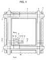
- FIG. 1is a plan view of the principal part of a thin film transistor panel in a liquid crystal display device as a first embodiment of the invention
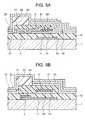
- FIG. 2Ais a sectional view taken along a line II A -II A in FIG. 1
- FIG. 2Bis a sectional view taken along a line II B -II B in FIG. 1 ;
- FIG. 3is a plan view of the principal part of a thin film transistor panel in a liquid crystal display device as a second embodiment of the invention
- FIG. 4Ais a sectional view taken along a line IV A -IV A in FIG. 3
- FIG. 4Bis a sectional view taken along a line IV B -IV B in FIG. 3 ;
- FIGS. 5A and 5Bare sectional views of the principal part of an organic electroluminescence (EL) display device as a third embodiment of the invention.
- FIGS. 6A and 6Bare sectional views of the principal part of an organic electroluminescence (EL) display device as a fourth embodiment of the invention.
- ELorganic electroluminescence
- FIG. 1shows a plan view of the principal part of a thin film transistor panel in a liquid crystal display device as a first embodiment of the present invention.
- FIG. 2Ashows a sectional view taken along a line II A -II A in FIG. 1
- FIG. 2Bshows a sectional view taken along a line II B -II B in FIG. 1 .
- the thin film transistor panelis provided with a glass substrate 1 .
- FIG. 1Numerous scanning lines 2 and numerous data lines 3 are formed on the top face side of the glass substrate 1 to be extended in directions to cross with each other at right angles.
- a display elementincluding a thin film transistor 5 connected to one corresponding scanning line 2 and one corresponding data line 3 , and a pixel electrode 4 electrically connected to the thin film transistor 5 is arranged in each region enclosed by both the lines 2 and 3 . The regions are arranged in a matrix.
- the edge portions of the pixel electrodes 4are hatched by oblique short solid lines.
- each of the square-like pixel electrodes 4is arranged in each of the square-like regions enclosed by the scanning lines 2 and the data lines 3 in the state in which the pixel electrode 4 is positioned as near as possible to the scanning lines 2 and the data lines 3 .
- Each of the thin film transistors 5is arranged on the under side in the lower left corner part of each of the pixel electrodes 4 in FIG. 1 , and almost the whole part of the thin film transistor 5 is covered by the pixel electrode 4 .
- the scanning lines 2are formed at predetermined positions on the top face of the glass substrate 1 .
- Gate electrodes 11are formed at predetermined positions on the top faces of the scanning lines 2 , and are severally formed in the neighborhood of the scanning lines 2 on the top face of the glass substrate 1 so as to cross with the scanning lines 2 at right angles (see FIG. 1 ). That is, one end portion of each of the gate electrodes 11 is formed on the top face of each of the scanning lines 2 .
- the gate electrodes 11are formed with a transparent metal oxide containing n type or p type impurities.
- n type impuritiesfor example, phosphorus, arsenic, antimony and the like can be cited.
- p type impuritiesfor example, boron, aluminum, gallium, indium and the like can be cited.
- a method of forming a film by a sputtering method using a metal oxide film including the n type or the p type impurities mentioned above as a target to pattern the formed film by using a photolithography techniqueis recommended.
- the n type metal oxide filmis generally suitable.
- the p type metal oxide filmcan be also used in case of regarding being low power consumption, but the use of the p type metal oxide film does not mean that the metal oxide film to be used for the formation of the gate electrodes 11 and the scanning lines 2 is limited to the p type metal oxide film.
- a gate insulating film 12 made of silicon nitrideis formed on the top face of the glass substrate 1 having the scanning lines 2 and the gate electrodes 11 thereon.
- Semiconductor thin films 13which severally have a band gap of 2.5 V or higher and are severally made of one of the transparent and intrinsic metal oxides mentioned above, are formed on the top face of the gate insulating film 12 on the gate electrodes 11 . Because the semiconductor thin films 13 severally having a wide band gap of 2.5 V or higher do not absorb any visible light, the semiconductor thin films 13 do not leak any light, and do not need light blocking consequently.
- Channel protecting films 14which are made of silicon nitride, are formed at almost the central parts of the top faces of the semiconductor thin films 13 .
- Each of the data lines 3is formed between corresponding two of the pixel electrodes 4 on the gate insulating film 12 .
- the width of each of the data lines 3is narrower than the gap of the two pixel electrodes 4 .
- the data lines 3are formed with a metal film having a light blocking property and a sufficiently small resistance value such as aluminum, chromium or the like.
- a source electrode 15 and a drain electrode 16are formed on both the sides of the top face of each of the channel protecting films 14 , and on the top face of a corresponding semiconductor thin film 13 on both the sides of the channel protecting film 14 .
- the materials of the metal oxide and the n type impuritiesare the same as those in case of the gate electrodes 11 .
- the drain electrode 16is formed to be extended so as to cross with the corresponding data line 3 at right angles so that the end of the extended portion is overlapped on the data line 3 (see FIG. 1 ).
- the source electrodes 15 and the drain electrodes 16are formed by the method of forming a film by the sputtering method using an n type metal oxide film as a target to pattern the source electrodes 15 and the drain electrodes 16 by using the photolithography technique similarly to the case of forming the gate electrodes 11 .
- each of the thin film transistors 5is composed of the gate electrode 11 , the gate insulating film 12 , the semiconductor thin film 13 , the channel protecting film 14 , the source electrode 15 and the drain electrode 16 .
- the gate electrode 11is formed of the transparent p type metal oxide or the transparent n type metal oxide
- the source electrode 15 and the drain electrode 16are formed of the transparent n type metal oxide
- the thin film transistor 5has a structure which transmits light.
- Overcoat films 17are formed on the top face of the gate insulating film 12 having the thin film transistors 5 and the data lines 3 thereon.
- Contact holes 18are formed at the portions of the overcoat films 17 corresponding to predetermined positions of the source electrodes 15 .
- Pixel electrodes (electrodes for pixels) 4which are made of a transparent electroconductive material such as ITO, are formed at predetermined positions of the overcoat films 17 to be electrically connected with the source electrodes 15 through the contact holes 18 . In this case, each of the pixel electrodes 4 is formed to cover almost the whole of each of the thin film transistors 5 .
- each of the thin film transistors 5has the structure transmitting light and almost the whole of the thin film transistor 5 is covered with each of the pixel electrodes 4 , all the area of the pixel electrode 4 including the thin film transistor 5 is a transmitting region, and the opening ratio of the pixel can be enlarged.
- the semiconductor thin film 13which is made of the transparent intrinsic metal oxide mentioned above, of the thin film transistor 5 , the semiconductor thin film 13 transmits the entered light as it is, and no problems are caused consequently.
- the scanning lines 2 and the data lines 3are formed with the light blocking metal film such as the aluminum, the chromium or the like in place of a transparent metal oxide including impurities, the light leakage between the pixel electrodes 4 can be prevented, and the resistance value can be made to be sufficiently small.
- FIG. 3shows a plan view of the principal part of a thin film transistor panel in a liquid crystal display device as a second embodiment of the present invention.
- FIG. 4Ashows a sectional view taken along a line IV A -IV A in FIG. 3
- FIG. 4Bshows a sectional view taken along a line IV B -IV B in FIG. 3 .
- the edge portions of the pixel electrodes 4are hatched by oblique short solid lines.
- the thin film transistor panelis different from the thin film transistor panel shown in FIGS. 1 , 2 A and 2 B in that the overcoat films 17 are omitted and each of the pixel electrodes 4 is formed with the n type metal oxide on one side of the top face of each of the channel protecting films 14 , on the top face of each of the semiconductor thin films 13 on the external side of the channel protecting film 14 , and at each of predetermined positions on the top face of the gate insulating film 12 to make a part of the pixel electrode 4 operate as a source electrode.
- the method described with regard to the first embodimentis used. That is, the scanning lines 2 , each made of a metal film having the light blocking property, and the gate electrodes 11 , each made of a transparent p type or n type metal oxide film, are formed on the top face of the glass substrate 1 .
- the gate insulating film 12is formed.
- the semiconductor thin films 13each made of a transparent intrinsic metal oxide
- the data lines 3each made of a metal film having the light blocking property
- an n type metal oxide filmis formed by the sputtering method, and the drain electrodes 16 and the pixel electrodes 4 are formed by the photolithographic method.
- the shapes of the pixel electrodes 4are made to be ones integrating each of the source electrodes and each of the pixel electrodes to be one body.
- the planer shape of each of the pixel electrodes 4is made to be one cut off at the corner part in the lower left of the pixel electrode in FIG. 3 .
- the overlapping part of the pixel electrode 4 and the gate electrode 11contributes to the opening ratio of the pixel. Consequently, the opening ratio can be enlarged.
- the pixel electrodes 4can be formed at the same process as those of the drain electrodes 16 , and it is unnecessary to form the over coat films 17 and the contact holes 18 to enable to reduce the number of processes.
- FIGS. 5A and 5Bshow the sectional views of the principal part of an organic electroluminescence (EL) display device as a third embodiment of the present invention.
- the same constituent elements as those of the thin film transistor panel shown in FIGS. 2A and 2Bare denoted by the same reference marks as those in FIGS. 2A and 2B , and their descriptions are omitted.
- the organic EL display devicelight emitting portions made of the organic EL are formed on the thin film transistors 5 . That is, the organic EL display device is configured as follows. Only the portion of each of the thin film transistors 5 except the corresponding source electrode 15 is covered by the corresponding overcoat film 17 .
- a corresponding anode electrode (an electrode for the pixel) 21is formed on the source electrode 15 , on a part of the overcoat film 17 , and on the gate insulating film 12 .
- a corresponding partition wall 22 made of polyimide or the likeis formed at a predetermined position on the top face of the overcoat film 17 and the gate insulating film 12 .
- a corresponding organic EL layer 23is formed on the top face of the anode electrode 21 between the partition wall 22 and a partition wall 22 in an adjacent pixel.
- a cathode electrode 24is formed on the top faces of the organic EL layers 23 and the partition walls 22 .
- the anode electrode 21is formed so as to cover almost the whole portion of the thin film transistor 5 .
- the anode electrode 21is formed with a transparent electroconductive material such as ITO or the like, and the cathode electrode 24 is formed with high reflexibility metal such as aluminum.
- the configurationbecause the light emitted from the organic EL layer 23 is reflected by the cathode electrode 24 , which is formed on the organic EL layer 23 , to be launched to the side of the glass substrate 1 , the configuration is called as a bottom emission type.
- the drain electrode 16 , the source electrode 15 , the semiconductor thin film 13 and the gate electrode 11are formed with the transparent metal oxide films, and because the thin film transistor 5 transmits the light which has been emitted from the organic EL layer 23 and has been reflected by the cathode electrode 24 , the whole region of the thin film transistor 5 becomes a light emitting region, and the opening ratio of the pixel can be enlarged.
- FIGS. 6A and 6Bshow the sectional views of the principal part of an organic EL display device as a fourth embodiment of the present invention.
- Each pixel of the organic EL display deviceis different from each pixel of the organic EL display device shown in FIGS. 5A and 5B in that the overcoat film 17 is omitted, and that the anode electrode 21 is formed with, for example, the transparent metal oxide including n type impurities on one side of the top face of the channel protecting film 14 , on the top face of the semiconductor thin film 13 on the external side of the channel protecting film 14 , and at a predetermined position on the top face of the gate insulating film 12 to make the anode electrode 21 operate also as a source electrode.
- predetermined corner parts of the anode electrode 21 , the organic EL layer 23 and the cathode electrode 24are cut off similarly to the case of cutting off the pixel electrode 4 at the corner part in the lower left of the pixel electrode 4 in FIG. 3 because the anode electrode 21 is formed on the same surface as that of the drain electrode 16 .
- the portion of the anode electrode 21 which functions as the source electrodenamely the portion formed on the channel protecting film 14 and the semiconductor thin film 13 , covers a part of the gate electrode 11 , the overlapping portion of the anode electrode 21 and the gate electrode 11 contributes to the opening ratio of the pixel, and consequently the opening ratio can be enlarged.
- the anode electrode 21can be formed at the same process as that of the drain electrode 16 , and consequently the number of processes can be reduced.
- each of the gate electrodes 11 and one end portion of each of the drain electrodes 16are formed on each top face of the corresponding scanning line 2 and the corresponding data line 3 , respectively, in, for example, FIGS. 1 , 2 A and 2 B
- the present inventionis not limited to such a configuration.
- the metal oxide film containing, for example, the n type impuritiesmay be formed, for example, on the whole of each top face of the scanning line 2 and the data line 3 .
- the scanning line 2 and the data line 3may be formed on the top face of each one end portion of the gate electrode 11 and the drain electrode 16 .
- the metal oxide film including, for example, the n type impuritiesmay be formed on the whole of each under surface of the scanning line 2 and the data line 3 .
- two thin film transistorsmay be formed in a pixel, which is composed of a group of one of the anode electrodes 21 , one of the organic EL layers 23 and the cathode electrode 24 (see, for example, JP 2004-171882 A).
- three thin film transistorsmay be formed in one pixel (see, for example, JP 2003-195810 A).
- the overlapping portion of the gate electrode of the thin film transistor and the electrode for the pixelcontributes to the opening ratio of the pixel, and consequently the opening ratio can be enlarged.
Landscapes
- Physics & Mathematics (AREA)
- Nonlinear Science (AREA)
- Microelectronics & Electronic Packaging (AREA)
- Engineering & Computer Science (AREA)
- Mathematical Physics (AREA)
- Crystallography & Structural Chemistry (AREA)
- Chemical & Material Sciences (AREA)
- General Physics & Mathematics (AREA)
- Optics & Photonics (AREA)
- Liquid Crystal (AREA)
- Thin Film Transistor (AREA)
- Devices For Indicating Variable Information By Combining Individual Elements (AREA)
- Electroluminescent Light Sources (AREA)
Abstract
Description
Claims (11)
Applications Claiming Priority (2)
| Application Number | Priority Date | Filing Date | Title |
|---|---|---|---|
| JP2005054403AJP5117667B2 (en) | 2005-02-28 | 2005-02-28 | Thin film transistor panel |
| JP2005-054403 | 2005-02-28 |
Publications (2)
| Publication Number | Publication Date |
|---|---|
| US20060192204A1 US20060192204A1 (en) | 2006-08-31 |
| US7795621B2true US7795621B2 (en) | 2010-09-14 |
Family
ID=36218101
Family Applications (1)
| Application Number | Title | Priority Date | Filing Date |
|---|---|---|---|
| US11/356,407Active2026-08-25US7795621B2 (en) | 2005-02-28 | 2006-02-16 | Thin film transistor panel |
Country Status (8)
| Country | Link |
|---|---|
| US (1) | US7795621B2 (en) |
| EP (1) | EP1854145A1 (en) |
| JP (1) | JP5117667B2 (en) |
| KR (1) | KR100869884B1 (en) |
| CN (1) | CN1943039B (en) |
| CA (1) | CA2562405A1 (en) |
| TW (1) | TWI303884B (en) |
| WO (1) | WO2006093028A1 (en) |
Cited By (10)
| Publication number | Priority date | Publication date | Assignee | Title |
|---|---|---|---|---|
| US20090283762A1 (en)* | 2008-05-16 | 2009-11-19 | Semiconductor Energy Laboratory Co., Ltd. | Semiconductor device and manufacturing method of the same |
| US20110156994A1 (en)* | 2009-12-24 | 2011-06-30 | Semiconductor Energy Laboratory Co., Ltd. | Display device |
| US8482004B2 (en) | 2009-10-09 | 2013-07-09 | Semiconductor Energy Laboratory Co., Ltd. | Light-emitting display device and electronic device including the same |
| US8835920B2 (en) | 2009-07-10 | 2014-09-16 | Semiconductor Energy Laboratory Co., Ltd. | Semiconductor device and method for manufacturing the same |
| US9768280B2 (en) | 2008-12-25 | 2017-09-19 | Semiconductor Energy Laboratory Co., Ltd. | Semiconductor device and manufacturing method thereof |
| US10461098B2 (en) | 2009-07-18 | 2019-10-29 | Semiconductor Energy Laboratory Co., Ltd. | Semiconductor device and method for manufacturing semiconductor device |
| US10629627B2 (en) | 2009-09-04 | 2020-04-21 | Semiconductor Energy Laboratory Co., Ltd. | Semiconductor device and manufacturing method thereof |
| US11189676B2 (en) | 2008-10-16 | 2021-11-30 | Semiconductor Energy Laboratory Co., Ltd. | Light-emitting device having fluorescent and phosphorescent materials |
| US11233132B2 (en) | 2009-03-05 | 2022-01-25 | Semiconductor Energy Laboratory Co., Ltd. | Semiconductor device |
| US12089459B2 (en) | 2019-05-10 | 2024-09-10 | Semiconductor Energy Laboratory Co., Ltd. | Display apparatus and electronic device |
Families Citing this family (25)
| Publication number | Priority date | Publication date | Assignee | Title |
|---|---|---|---|---|
| JP2006245031A (en)* | 2005-02-28 | 2006-09-14 | Casio Comput Co Ltd | Thin film transistor panel |
| JP4934599B2 (en)* | 2007-01-29 | 2012-05-16 | キヤノン株式会社 | Active matrix display device |
| CN101325201B (en)* | 2007-06-13 | 2011-04-13 | 北京京东方光电科技有限公司 | Array substrate structure of transparent film transistor and manufacturing method thereof |
| KR100847846B1 (en)* | 2007-08-01 | 2008-07-23 | 실리콘 디스플레이 (주) | Method of manufacturing thin film transistor using local doping |
| KR100907255B1 (en)* | 2007-09-18 | 2009-07-10 | 한국전자통신연구원 | Display device provided with organic thin film transistor |
| JP2009175198A (en) | 2008-01-21 | 2009-08-06 | Sony Corp | El display panel and electronic apparatus |
| JP5248148B2 (en)* | 2008-03-10 | 2013-07-31 | 株式会社ポッカコーポレーション | Anti-methicillin-resistant Staphylococcus aureus and anti-vancomycin-resistant enterococci |
| JP5491833B2 (en)* | 2008-12-05 | 2014-05-14 | 株式会社半導体エネルギー研究所 | Semiconductor device |
| US20100224880A1 (en)* | 2009-03-05 | 2010-09-09 | Semiconductor Energy Laboratory Co., Ltd. | Semiconductor device |
| TW201103090A (en)* | 2009-07-01 | 2011-01-16 | Univ Nat Chiao Tung | Method for manufacturing a self-aligned thin film transistor and a structure of the same |
| WO2011010545A1 (en)* | 2009-07-18 | 2011-01-27 | Semiconductor Energy Laboratory Co., Ltd. | Semiconductor device and method for manufacturing the same |
| CN105070749B (en)* | 2009-07-18 | 2019-08-09 | 株式会社半导体能源研究所 | Semiconductor device and method of manufacturing semiconductor device |
| WO2011010542A1 (en)* | 2009-07-23 | 2011-01-27 | Semiconductor Energy Laboratory Co., Ltd. | Semiconductor device and method for manufacturing the same |
| TWI596741B (en)* | 2009-08-07 | 2017-08-21 | 半導體能源研究所股份有限公司 | Semiconductor device and method of manufacturing same |
| WO2011027702A1 (en)* | 2009-09-04 | 2011-03-10 | Semiconductor Energy Laboratory Co., Ltd. | Light-emitting device and method for manufacturing the same |
| CN102023433B (en)* | 2009-09-18 | 2012-02-29 | 北京京东方光电科技有限公司 | TFT-LCD array substrate and manufacturing method thereof |
| CN102598278B (en)* | 2009-10-09 | 2015-04-08 | 株式会社半导体能源研究所 | Semiconductor device |
| KR101779349B1 (en)* | 2009-10-14 | 2017-09-18 | 가부시키가이샤 한도오따이 에네루기 켄큐쇼 | Semiconductor device and manufacturing method thereof |
| US8569754B2 (en) | 2010-11-05 | 2013-10-29 | Semiconductor Energy Laboratory Co., Ltd. | Semiconductor device and manufacturing method thereof |
| JP2013206919A (en)* | 2012-03-27 | 2013-10-07 | Sony Corp | Thin film transistor, manufacturing method of the same and display device |
| CN104752467A (en)* | 2013-12-30 | 2015-07-01 | 昆山国显光电有限公司 | Organic light emitting display device and preparation method thereof |
| GB2566673B (en)* | 2017-07-21 | 2022-10-26 | Flexenable Ltd | Thin-Film Transistor (TFT) Architecture for Liquid Crystal Displays |
| CN107768386B (en) | 2017-11-16 | 2020-09-01 | 深圳市华星光电半导体显示技术有限公司 | TFT array substrate and its manufacturing method and liquid crystal display panel |
| TWI721776B (en)* | 2020-02-06 | 2021-03-11 | 友達光電股份有限公司 | Active device substrate and manufactturing method thereof |
| CN114265249B (en)* | 2021-12-16 | 2023-06-02 | Tcl华星光电技术有限公司 | An array substrate and a display terminal |
Citations (25)
| Publication number | Priority date | Publication date | Assignee | Title |
|---|---|---|---|---|
| CN1079826A (en) | 1992-04-22 | 1993-12-22 | 国际商业机器公司 | Liquid crystal display device |
| EP0595363A1 (en) | 1992-10-30 | 1994-05-04 | Nec Corporation | Transmission type active matrix liquid crystal device |
| US5744864A (en) | 1995-08-03 | 1998-04-28 | U.S. Philips Corporation | Semiconductor device having a transparent switching element |
| US6040882A (en) | 1996-10-16 | 2000-03-21 | Hyundai Electronics Industries Co., Ltd. | Liquid crystal display device having "H" character common electrode and method of fabricating thereof |
| US6069370A (en)* | 1997-03-26 | 2000-05-30 | Nec Corporation | Field-effect transistor and fabrication method thereof and image display apparatus |
| US6303963B1 (en)* | 1998-12-03 | 2001-10-16 | Semiconductor Energy Laboratory Co., Ltd. | Electro-optical device and semiconductor circuit |
| US20020058362A1 (en) | 1998-02-26 | 2002-05-16 | Hisashi Ohtani | Active matrix type display device and method of manufacturing the same |
| US20020063810A1 (en) | 2000-11-27 | 2002-05-30 | Mutsumi Nakajima | Liquid crystal display device |
| US6509616B2 (en) | 2000-09-29 | 2003-01-21 | Semiconductor Energy Laboratory Co., Ltd. | Semiconductor device and its manufacturing method |
| JP2003050405A (en) | 2000-11-15 | 2003-02-21 | Matsushita Electric Ind Co Ltd | Thin film transistor array, method of manufacturing the same, and display panel using the same |
| US20030111663A1 (en) | 2001-12-13 | 2003-06-19 | Fuji Xerox Co., Ltd. | Thin film transistor and display device having the same |
| US6610997B2 (en) | 2000-03-17 | 2003-08-26 | Seiko Epson Corporation | Electro-optical device |
| JP2003243154A (en) | 2002-02-18 | 2003-08-29 | Fuji Electric Co Ltd | Organic EL display |
| US20030168688A1 (en) | 1997-03-28 | 2003-09-11 | Semiconductor Energy Laboratory Co., Ltd. | Active matrix liquid crystal display device |
| US20030203545A1 (en) | 2001-02-28 | 2003-10-30 | Semiconductor Energy Laboratory Co., Ltd. | Method of manufacturing a semiconductor device |
| US20030218222A1 (en) | 2002-05-21 | 2003-11-27 | The State Of Oregon Acting And Through The Oregon State Board Of Higher Education On Behalf Of | Transistor structures and methods for making the same |
| US20030218221A1 (en) | 2002-05-21 | 2003-11-27 | the State of Oregon acting by and through the behalf of Oregon State University | Transistor structures and methods for making the same |
| US6674495B1 (en)* | 1999-09-30 | 2004-01-06 | Samsung Electronics Co., Ltd. | Thin film transistor array panel for a liquid crystal display and methods for manufacturing the same |
| JP2004014982A (en) | 2002-06-11 | 2004-01-15 | Konica Minolta Holdings Inc | Semiconductor circuit and image display device |
| US20040155846A1 (en) | 2003-02-07 | 2004-08-12 | Randy Hoffman | Transparent active-matrix display |
| US20040155270A1 (en) | 2003-02-07 | 2004-08-12 | Randy Hoffman | Transparent double-injection field-effect transistor |
| US20050001945A1 (en) | 2003-05-22 | 2005-01-06 | Seiko Epson Corporation | Electro-optical device, electronic apparatus, and projection display apparatus |
| US20060194500A1 (en) | 2005-02-28 | 2006-08-31 | Casio Computer Co., Ltd. | Thin film transistor panel |
| US7319239B2 (en) | 2004-05-25 | 2008-01-15 | Sharp Kabushiki Kaisha | Substrate for display device having a protective layer provided between the pixel electrodes and wirings of the active matrix substrate, manufacturing method for same, and display device |
| US7495387B2 (en)* | 2001-02-05 | 2009-02-24 | Samsung Sdi Co., Ltd. | Organic electroluminescent element and organic electroluminescent device including the same |
Family Cites Families (10)
| Publication number | Priority date | Publication date | Assignee | Title |
|---|---|---|---|---|
| GB2203881B (en)* | 1987-04-16 | 1991-03-27 | Philips Electronic Associated | Liquid crystal display device |
| JPH07119914B2 (en)* | 1989-01-27 | 1995-12-20 | 日本電気株式会社 | Thin film field effect transistor element array |
| JPH05251705A (en)* | 1992-03-04 | 1993-09-28 | Fuji Xerox Co Ltd | Thin-film transistor |
| JPH09105952A (en)* | 1995-10-11 | 1997-04-22 | Toshiba Electron Eng Corp | Active matrix type liquid crystal display |
| JP3367821B2 (en)* | 1996-06-03 | 2003-01-20 | シャープ株式会社 | Active matrix substrate |
| JP3750303B2 (en)* | 1997-09-11 | 2006-03-01 | ソニー株式会社 | Liquid crystal display |
| JP2000298440A (en)* | 1999-02-08 | 2000-10-24 | Tdk Corp | Matrix display device |
| JP2001209331A (en)* | 2000-01-27 | 2001-08-03 | Tdk Corp | Thin film display device |
| JP2002108250A (en)* | 2000-09-29 | 2002-04-10 | Sharp Corp | Active matrix drive type self-luminous display device and manufacturing method thereof |
| TW594232B (en)* | 2002-11-26 | 2004-06-21 | Hannstar Display Corp | A method of utilizing dual-layer photoresist to form black matrix and spacers on a control circuit substrate |
- 2005
- 2005-02-28JPJP2005054403Apatent/JP5117667B2/ennot_activeExpired - Lifetime
- 2006
- 2006-02-16USUS11/356,407patent/US7795621B2/enactiveActive
- 2006-02-17CACA002562405Apatent/CA2562405A1/ennot_activeAbandoned
- 2006-02-17CNCN2006800001756Apatent/CN1943039B/enactiveActive
- 2006-02-17EPEP20060714488patent/EP1854145A1/ennot_activeCeased
- 2006-02-17WOPCT/JP2006/303348patent/WO2006093028A1/enactiveApplication Filing
- 2006-02-17KRKR1020067022044Apatent/KR100869884B1/enactiveActive
- 2006-02-27TWTW095106498Apatent/TWI303884B/enactive
Patent Citations (30)
| Publication number | Priority date | Publication date | Assignee | Title |
|---|---|---|---|---|
| US5510916A (en) | 1992-01-30 | 1996-04-23 | Nec Corporation | Active matrix liquid crystal device with opposite substrate having black matrix with larger aperture than active substrate |
| CN1079826A (en) | 1992-04-22 | 1993-12-22 | 国际商业机器公司 | Liquid crystal display device |
| US5345324A (en) | 1992-04-22 | 1994-09-06 | International Business Machines Corporation | Active matrix liquid crystal display device having two light shielding layers |
| EP0595363A1 (en) | 1992-10-30 | 1994-05-04 | Nec Corporation | Transmission type active matrix liquid crystal device |
| US5744864A (en) | 1995-08-03 | 1998-04-28 | U.S. Philips Corporation | Semiconductor device having a transparent switching element |
| US6040882A (en) | 1996-10-16 | 2000-03-21 | Hyundai Electronics Industries Co., Ltd. | Liquid crystal display device having "H" character common electrode and method of fabricating thereof |
| US6069370A (en)* | 1997-03-26 | 2000-05-30 | Nec Corporation | Field-effect transistor and fabrication method thereof and image display apparatus |
| US20030168688A1 (en) | 1997-03-28 | 2003-09-11 | Semiconductor Energy Laboratory Co., Ltd. | Active matrix liquid crystal display device |
| US20020058362A1 (en) | 1998-02-26 | 2002-05-16 | Hisashi Ohtani | Active matrix type display device and method of manufacturing the same |
| US6303963B1 (en)* | 1998-12-03 | 2001-10-16 | Semiconductor Energy Laboratory Co., Ltd. | Electro-optical device and semiconductor circuit |
| US6674495B1 (en)* | 1999-09-30 | 2004-01-06 | Samsung Electronics Co., Ltd. | Thin film transistor array panel for a liquid crystal display and methods for manufacturing the same |
| US6610997B2 (en) | 2000-03-17 | 2003-08-26 | Seiko Epson Corporation | Electro-optical device |
| US6509616B2 (en) | 2000-09-29 | 2003-01-21 | Semiconductor Energy Laboratory Co., Ltd. | Semiconductor device and its manufacturing method |
| JP2003050405A (en) | 2000-11-15 | 2003-02-21 | Matsushita Electric Ind Co Ltd | Thin film transistor array, method of manufacturing the same, and display panel using the same |
| US20020063810A1 (en) | 2000-11-27 | 2002-05-30 | Mutsumi Nakajima | Liquid crystal display device |
| US7495387B2 (en)* | 2001-02-05 | 2009-02-24 | Samsung Sdi Co., Ltd. | Organic electroluminescent element and organic electroluminescent device including the same |
| US20030203545A1 (en) | 2001-02-28 | 2003-10-30 | Semiconductor Energy Laboratory Co., Ltd. | Method of manufacturing a semiconductor device |
| US6713785B2 (en)* | 2001-12-13 | 2004-03-30 | Fuji Xerox Co., Ltd. | Thin film transistor and display device having the same |
| US20030111663A1 (en) | 2001-12-13 | 2003-06-19 | Fuji Xerox Co., Ltd. | Thin film transistor and display device having the same |
| JP2003243154A (en) | 2002-02-18 | 2003-08-29 | Fuji Electric Co Ltd | Organic EL display |
| US20030218221A1 (en) | 2002-05-21 | 2003-11-27 | the State of Oregon acting by and through the behalf of Oregon State University | Transistor structures and methods for making the same |
| US20030218222A1 (en) | 2002-05-21 | 2003-11-27 | The State Of Oregon Acting And Through The Oregon State Board Of Higher Education On Behalf Of | Transistor structures and methods for making the same |
| JP2004014982A (en) | 2002-06-11 | 2004-01-15 | Konica Minolta Holdings Inc | Semiconductor circuit and image display device |
| US20040155846A1 (en) | 2003-02-07 | 2004-08-12 | Randy Hoffman | Transparent active-matrix display |
| US20040155270A1 (en) | 2003-02-07 | 2004-08-12 | Randy Hoffman | Transparent double-injection field-effect transistor |
| US20060033108A1 (en) | 2003-02-07 | 2006-02-16 | Randy Hoffman | Transparent double-injection field-effect transistor |
| US20050001945A1 (en) | 2003-05-22 | 2005-01-06 | Seiko Epson Corporation | Electro-optical device, electronic apparatus, and projection display apparatus |
| US7319239B2 (en) | 2004-05-25 | 2008-01-15 | Sharp Kabushiki Kaisha | Substrate for display device having a protective layer provided between the pixel electrodes and wirings of the active matrix substrate, manufacturing method for same, and display device |
| US20060194500A1 (en) | 2005-02-28 | 2006-08-31 | Casio Computer Co., Ltd. | Thin film transistor panel |
| US7633090B2 (en)* | 2005-02-28 | 2009-12-15 | Casio Computer Co., Ltd. | Thin film transistor panel |
Non-Patent Citations (6)
| Title |
|---|
| Chinese Office Action dated Apr. 10, 2009 (6 pages), and English translation thereof (5 pages), issued in counterpart Chinese Application Serial No. 200680000175.6. |
| Chinese Office Action dated Sep. 25, 2009 and English translation thereof issued in a counterpart Chinese Application No. 200680006042X of related U.S. Appl. No. 11/357,595. |
| Japanese Office Action dated Sep. 29, 2009 and English translation thereof issued in counterpart Japanese Application No. 2005-054402 of related U.S. Appl. No. 11/357,595. |
| Notification Concerning Transmittal of International Preliminary Report on Patentability, Chapter I of the Patent Cooperation Treaty, and Written Opinion of the International Searching Authority, dated Sep. 11, 2007, for PCT/JP2006/303348 8 sheets. |
| Ohta, H. et al., "Frontier of Transparent Oxide Semiconductor" solid State Electronics, Elsevier Science Publishers, Barking, GB, vol. 47, No. 12, Dec. 2003, pp. 2261-2267, XP004464944, ISSN: 0038-1101. |
| Related U.S. Appl. No. 11/357,595, filed Feb. 17, 2006; Inventor: H. Ishii. |
Cited By (43)
| Publication number | Priority date | Publication date | Assignee | Title |
|---|---|---|---|---|
| US10580797B2 (en) | 2008-05-16 | 2020-03-03 | Semiconductor Energy Laboratory Co., Ltd. | Semiconductor device and manufacturing method of the same |
| US12300702B2 (en) | 2008-05-16 | 2025-05-13 | Semiconductor Energy Laboratory Co., Ltd. | Semiconductor device including storage capacitor having pixel electrode, directly stacked conductive layer, and insulating layer interposed between them, wherein the stacked conductive layers extending towards the gate and source wirings/lines |
| US11646322B2 (en) | 2008-05-16 | 2023-05-09 | Semiconductor Energy Laboratory Co., Ltd. | Semiconductor device having conductive oxide electrode layers in direct contact with oxide semiconductor layer |
| US9041202B2 (en) | 2008-05-16 | 2015-05-26 | Semiconductor Energy Laboratory Co., Ltd. | Semiconductor device and manufacturing method of the same |
| US11133332B2 (en) | 2008-05-16 | 2021-09-28 | Semiconductor Energy Laboratory Co., Ltd. | Semiconductor device and manufacturing method of the same |
| US20090283762A1 (en)* | 2008-05-16 | 2009-11-19 | Semiconductor Energy Laboratory Co., Ltd. | Semiconductor device and manufacturing method of the same |
| US9397255B2 (en) | 2008-05-16 | 2016-07-19 | Semiconductor Energy Laboratory Co., Ltd. | Semiconductor device and manufacturing method of the same |
| US11930668B2 (en) | 2008-10-16 | 2024-03-12 | Semiconductor Energy Laboratory Co., Ltd. | Flexible light-emitting device and EL module including transparent conductive film |
| US11189676B2 (en) | 2008-10-16 | 2021-11-30 | Semiconductor Energy Laboratory Co., Ltd. | Light-emitting device having fluorescent and phosphorescent materials |
| US10720451B2 (en) | 2008-12-25 | 2020-07-21 | Semiconductor Energy Laboratory Co., Ltd. | Semiconductor device and manufacturing method thereof |
| US11158654B2 (en) | 2008-12-25 | 2021-10-26 | Semiconductor Energy Laboratory Co., Ltd. | Semiconductor device and manufacturing method thereof |
| US9768280B2 (en) | 2008-12-25 | 2017-09-19 | Semiconductor Energy Laboratory Co., Ltd. | Semiconductor device and manufacturing method thereof |
| US11996416B2 (en) | 2008-12-25 | 2024-05-28 | Semiconductor Energy Laboratory Co., Ltd. | Semiconductor device and manufacturing method thereof |
| US10483290B2 (en) | 2008-12-25 | 2019-11-19 | Semiconductor Energy Laboratory Co., Ltd. | Semiconductor device and manufacturing method thereof |
| US11961894B2 (en) | 2009-03-05 | 2024-04-16 | Semiconductor Energy Laboratory Co., Ltd. | Semiconductor device |
| US11233132B2 (en) | 2009-03-05 | 2022-01-25 | Semiconductor Energy Laboratory Co., Ltd. | Semiconductor device |
| US9054138B2 (en) | 2009-07-10 | 2015-06-09 | Semiconductor Energy Laboratory Co., Ltd. | Semiconductor device and method for manufacturing the same |
| US10157936B2 (en) | 2009-07-10 | 2018-12-18 | Semiconductor Energy Laboratory Co., Ltd. | Semiconductor device and method for manufacturing the same |
| US9490277B2 (en) | 2009-07-10 | 2016-11-08 | Semiconductor Energy Laboratory Co., Ltd. | Semiconductor device and method for manufacturing the same |
| US8835920B2 (en) | 2009-07-10 | 2014-09-16 | Semiconductor Energy Laboratory Co., Ltd. | Semiconductor device and method for manufacturing the same |
| US11374029B2 (en) | 2009-07-10 | 2022-06-28 | Semiconductor Energy Laboratory Co., Ltd. | Semiconductor device and method for manufacturing the same |
| US9754974B2 (en) | 2009-07-10 | 2017-09-05 | Semiconductor Energy Laboratory Co., Ltd. | Semiconductor device and method for manufacturing the same |
| US10916566B2 (en) | 2009-07-10 | 2021-02-09 | Semiconductor Energy Laboratory Co., Ltd. | Semiconductor device and method for manufacturing the same |
| US12057453B2 (en) | 2009-07-10 | 2024-08-06 | Semiconductor Energy Laboratory Co., Ltd. | Semiconductor device and method for manufacturing the same |
| US10522568B2 (en) | 2009-07-10 | 2019-12-31 | Semiconductor Energy Laboratory Co., Ltd. | Semiconductor device and method for manufacturing the same |
| US11177289B2 (en) | 2009-07-18 | 2021-11-16 | Semiconductor Energy Laboratory Co., Ltd. | Semiconductor device and method for manufacturing semiconductor device |
| US10461098B2 (en) | 2009-07-18 | 2019-10-29 | Semiconductor Energy Laboratory Co., Ltd. | Semiconductor device and method for manufacturing semiconductor device |
| US11715741B2 (en) | 2009-07-18 | 2023-08-01 | Semiconductor Energy Laboratory Co., Ltd. | Semiconductor device and method for manufacturing semiconductor device |
| US10854640B2 (en) | 2009-09-04 | 2020-12-01 | Semiconductor Energy Laboratory Co., Ltd. | Semiconductor device and manufacturing method thereof |
| US12002818B2 (en) | 2009-09-04 | 2024-06-04 | Semiconductor Energy Laboratory Co., Ltd. | Semiconductor device and manufacturing method thereof |
| US12408435B2 (en) | 2009-09-04 | 2025-09-02 | Semiconductor Energy Laboratory Co., Ltd. | Semiconductor device and manufacturing method thereof |
| US10629627B2 (en) | 2009-09-04 | 2020-04-21 | Semiconductor Energy Laboratory Co., Ltd. | Semiconductor device and manufacturing method thereof |
| US11695019B2 (en) | 2009-09-04 | 2023-07-04 | Semiconductor Energy Laboratory Co., Ltd. | Semiconductor device and manufacturing method thereof |
| US10411158B2 (en) | 2009-10-09 | 2019-09-10 | Semiconductor Energy Laboratory Co., Ltd. | Light-emitting display device having oxide semiconductor layer overlapping with adjacent pixel electrode |
| US8482004B2 (en) | 2009-10-09 | 2013-07-09 | Semiconductor Energy Laboratory Co., Ltd. | Light-emitting display device and electronic device including the same |
| US10566497B2 (en) | 2009-10-09 | 2020-02-18 | Semiconductor Energy Laboratory Co., Ltd. | Light-emitting display device including a first pixel and a second pixel |
| US11901485B2 (en) | 2009-10-09 | 2024-02-13 | Semiconductor Energy Laboratory Co., Ltd. | Light-emitting display device having a first pixel and a second pixel and an oxide semiconductor layer having a region overlapping a light-emitting region of the second pixel |
| US11355669B2 (en) | 2009-10-09 | 2022-06-07 | Semiconductor Energy Laboratory Co., Ltd. | Light-emitting display device and electronic device including an oxide semiconductor layer |
| US12224376B2 (en) | 2009-10-09 | 2025-02-11 | Semiconductor Energy Laboratory Co., Ltd. | Light-emitting display device and electronic device including a first pixel and a second pixel and an oxide semiconductor region overlapping a light-emitting region |
| US9318654B2 (en) | 2009-10-09 | 2016-04-19 | Semiconductor Energy Laboratory Co., Ltd. | Light-emitting display device and electronic device including the same |
| US9217903B2 (en) | 2009-12-24 | 2015-12-22 | Semiconductor Energy Laboratory Co., Ltd. | Display device |
| US20110156994A1 (en)* | 2009-12-24 | 2011-06-30 | Semiconductor Energy Laboratory Co., Ltd. | Display device |
| US12089459B2 (en) | 2019-05-10 | 2024-09-10 | Semiconductor Energy Laboratory Co., Ltd. | Display apparatus and electronic device |
Also Published As
| Publication number | Publication date |
|---|---|
| JP2006242987A (en) | 2006-09-14 |
| KR100869884B1 (en) | 2008-11-24 |
| EP1854145A1 (en) | 2007-11-14 |
| US20060192204A1 (en) | 2006-08-31 |
| WO2006093028A1 (en) | 2006-09-08 |
| CN1943039B (en) | 2012-11-21 |
| CA2562405A1 (en) | 2006-09-08 |
| KR20070088288A (en) | 2007-08-29 |
| JP5117667B2 (en) | 2013-01-16 |
| TW200640014A (en) | 2006-11-16 |
| CN1943039A (en) | 2007-04-04 |
| TWI303884B (en) | 2008-12-01 |
Similar Documents
| Publication | Publication Date | Title |
|---|---|---|
| US7795621B2 (en) | Thin film transistor panel | |
| US7633090B2 (en) | Thin film transistor panel | |
| JP3695308B2 (en) | Active matrix organic EL display device and manufacturing method thereof | |
| US12310199B2 (en) | Display substrate and display apparatus | |
| KR100557730B1 (en) | Dual panel type organic electroluminescent device and manufacturing method thereof | |
| US10439010B2 (en) | Display device | |
| US11782562B2 (en) | Touch panel, touch display panel, and electronic device | |
| KR102295477B1 (en) | Thin film transistor array panel | |
| KR100653265B1 (en) | Dual panel type organic electroluminescent device and manufacturing method thereof | |
| CN113937236A (en) | Display substrate, preparation method thereof and display device | |
| KR20170012664A (en) | Thin Film Transistor Array Substrate And Organic Light Emitting Diode Display Device Including The Same | |
| KR20140022523A (en) | Thin film transistor substrate and method for manufacturing that same and organic light emitting device using that same | |
| KR101957145B1 (en) | Organic Light Emitting diode display and method of manufacturing the same | |
| US6504593B1 (en) | Display electrode arrangement for a reflection type liquid crystal display device | |
| KR100482166B1 (en) | Dual Panel Type Organic Electroluminescent Device and Method for Fabricating the same | |
| KR20050069314A (en) | Dual panel type organic electroluminescent device and method for fabricating the same | |
| JP2006024610A (en) | Thin-film transistor and display device | |
| US12068332B2 (en) | Display panel and display device | |
| US20250221171A1 (en) | Light emitting display device | |
| CN120113362A (en) | Array substrate and manufacturing method thereof, and display panel |
Legal Events
| Date | Code | Title | Description |
|---|---|---|---|
| AS | Assignment | Owner name:CASIO COMPUTER CO., LTD., JAPAN Free format text:ASSIGNMENT OF ASSIGNORS INTEREST;ASSIGNORS:YAMAGUCHI, IKUHIRO;TAKEI, MANABU;YOSHIDA, MOTOHIKO;REEL/FRAME:017651/0811 Effective date:20060120 | |
| FEPP | Fee payment procedure | Free format text:PAYOR NUMBER ASSIGNED (ORIGINAL EVENT CODE: ASPN); ENTITY STATUS OF PATENT OWNER: LARGE ENTITY | |
| STCF | Information on status: patent grant | Free format text:PATENTED CASE | |
| FEPP | Fee payment procedure | Free format text:PAYOR NUMBER ASSIGNED (ORIGINAL EVENT CODE: ASPN); ENTITY STATUS OF PATENT OWNER: LARGE ENTITY Free format text:PAYER NUMBER DE-ASSIGNED (ORIGINAL EVENT CODE: RMPN); ENTITY STATUS OF PATENT OWNER: LARGE ENTITY | |
| AS | Assignment | Owner name:REMSEN INNOVATION, LLC, DISTRICT OF COLUMBIA Free format text:ASSIGNMENT OF ASSIGNORS INTEREST;ASSIGNOR:CASIO COMPUTER CO., LTD.;REEL/FRAME:028265/0258 Effective date:20120510 | |
| AS | Assignment | Owner name:SAMSUNG DISPLAY CO., LTD., KOREA, REPUBLIC OF Free format text:ASSIGNMENT OF ASSIGNORS INTEREST;ASSIGNOR:REMSEN INNOVATION, LLC;REEL/FRAME:030951/0988 Effective date:20130729 | |
| FPAY | Fee payment | Year of fee payment:4 | |
| MAFP | Maintenance fee payment | Free format text:PAYMENT OF MAINTENANCE FEE, 8TH YEAR, LARGE ENTITY (ORIGINAL EVENT CODE: M1552) Year of fee payment:8 | |
| MAFP | Maintenance fee payment | Free format text:PAYMENT OF MAINTENANCE FEE, 12TH YEAR, LARGE ENTITY (ORIGINAL EVENT CODE: M1553); ENTITY STATUS OF PATENT OWNER: LARGE ENTITY Year of fee payment:12 |