US7795076B2 - Method, system, and apparatus for transfer of dies using a die plate having die cavities - Google Patents
Method, system, and apparatus for transfer of dies using a die plate having die cavitiesDownload PDFInfo
- Publication number
- US7795076B2 US7795076B2US10/866,150US86615004AUS7795076B2US 7795076 B2US7795076 B2US 7795076B2US 86615004 AUS86615004 AUS 86615004AUS 7795076 B2US7795076 B2US 7795076B2
- Authority
- US
- United States
- Prior art keywords
- die
- dies
- support structure
- cells
- receptacle structure
- Prior art date
- Legal status (The legal status is an assumption and is not a legal conclusion. Google has not performed a legal analysis and makes no representation as to the accuracy of the status listed.)
- Expired - Lifetime, expires
Links
Images


Classifications
- H—ELECTRICITY
- H01—ELECTRIC ELEMENTS
- H01L—SEMICONDUCTOR DEVICES NOT COVERED BY CLASS H10
- H01L24/00—Arrangements for connecting or disconnecting semiconductor or solid-state bodies; Methods or apparatus related thereto
- H01L24/93—Batch processes
- H01L24/95—Batch processes at chip-level, i.e. with connecting carried out on a plurality of singulated devices, i.e. on diced chips
- G—PHYSICS
- G06—COMPUTING OR CALCULATING; COUNTING
- G06K—GRAPHICAL DATA READING; PRESENTATION OF DATA; RECORD CARRIERS; HANDLING RECORD CARRIERS
- G06K19/00—Record carriers for use with machines and with at least a part designed to carry digital markings
- G06K19/04—Record carriers for use with machines and with at least a part designed to carry digital markings characterised by the shape
- G06K19/041—Constructional details
- G06K19/042—Constructional details the record carrier having a form factor of a credit card and including a small sized disc, e.g. a CD or DVD
- G06K19/045—Constructional details the record carrier having a form factor of a credit card and including a small sized disc, e.g. a CD or DVD the record carrier being of the non-contact type, e.g. RFID, and being specially adapted for attachment to a disc, e.g. a CD or DVD
- G—PHYSICS
- G06—COMPUTING OR CALCULATING; COUNTING
- G06K—GRAPHICAL DATA READING; PRESENTATION OF DATA; RECORD CARRIERS; HANDLING RECORD CARRIERS
- G06K19/00—Record carriers for use with machines and with at least a part designed to carry digital markings
- G06K19/06—Record carriers for use with machines and with at least a part designed to carry digital markings characterised by the kind of the digital marking, e.g. shape, nature, code
- G06K19/067—Record carriers with conductive marks, printed circuits or semiconductor circuit elements, e.g. credit or identity cards also with resonating or responding marks without active components
- G06K19/07—Record carriers with conductive marks, printed circuits or semiconductor circuit elements, e.g. credit or identity cards also with resonating or responding marks without active components with integrated circuit chips
- G06K19/077—Constructional details, e.g. mounting of circuits in the carrier
- G06K19/07718—Constructional details, e.g. mounting of circuits in the carrier the record carrier being manufactured in a continuous process, e.g. using endless rolls
- G—PHYSICS
- G06—COMPUTING OR CALCULATING; COUNTING
- G06K—GRAPHICAL DATA READING; PRESENTATION OF DATA; RECORD CARRIERS; HANDLING RECORD CARRIERS
- G06K7/00—Methods or arrangements for sensing record carriers, e.g. for reading patterns
- G06K7/0095—Testing the sensing arrangement, e.g. testing if a magnetic card reader, bar code reader, RFID interrogator or smart card reader functions properly
- G—PHYSICS
- G11—INFORMATION STORAGE
- G11B—INFORMATION STORAGE BASED ON RELATIVE MOVEMENT BETWEEN RECORD CARRIER AND TRANSDUCER
- G11B23/00—Record carriers not specific to the method of recording or reproducing; Accessories, e.g. containers, specially adapted for co-operation with the recording or reproducing apparatus ; Intermediate mediums; Apparatus or processes specially adapted for their manufacture
- G11B23/0014—Record carriers not specific to the method of recording or reproducing; Accessories, e.g. containers, specially adapted for co-operation with the recording or reproducing apparatus ; Intermediate mediums; Apparatus or processes specially adapted for their manufacture record carriers not specifically of filamentary or web form
- G11B23/0021—Record carriers not specific to the method of recording or reproducing; Accessories, e.g. containers, specially adapted for co-operation with the recording or reproducing apparatus ; Intermediate mediums; Apparatus or processes specially adapted for their manufacture record carriers not specifically of filamentary or web form discs
- G11B23/0028—Details
- G11B23/0035—Details means incorporated in the disc, e.g. hub, to enable its guiding, loading or driving
- G11B23/0042—Details means incorporated in the disc, e.g. hub, to enable its guiding, loading or driving with provision for auxiliary features
- H—ELECTRICITY
- H01—ELECTRIC ELEMENTS
- H01L—SEMICONDUCTOR DEVICES NOT COVERED BY CLASS H10
- H01L21/00—Processes or apparatus adapted for the manufacture or treatment of semiconductor or solid state devices or of parts thereof
- H01L21/67—Apparatus specially adapted for handling semiconductor or electric solid state devices during manufacture or treatment thereof; Apparatus specially adapted for handling wafers during manufacture or treatment of semiconductor or electric solid state devices or components ; Apparatus not specifically provided for elsewhere
- H01L21/67005—Apparatus not specifically provided for elsewhere
- H01L21/67011—Apparatus for manufacture or treatment
- H01L21/67132—Apparatus for placing on an insulating substrate, e.g. tape
- H—ELECTRICITY
- H01—ELECTRIC ELEMENTS
- H01L—SEMICONDUCTOR DEVICES NOT COVERED BY CLASS H10
- H01L21/00—Processes or apparatus adapted for the manufacture or treatment of semiconductor or solid state devices or of parts thereof
- H01L21/67—Apparatus specially adapted for handling semiconductor or electric solid state devices during manufacture or treatment thereof; Apparatus specially adapted for handling wafers during manufacture or treatment of semiconductor or electric solid state devices or components ; Apparatus not specifically provided for elsewhere
- H01L21/67005—Apparatus not specifically provided for elsewhere
- H01L21/67011—Apparatus for manufacture or treatment
- H01L21/67144—Apparatus for mounting on conductive members, e.g. leadframes or conductors on insulating substrates
- H—ELECTRICITY
- H01—ELECTRIC ELEMENTS
- H01L—SEMICONDUCTOR DEVICES NOT COVERED BY CLASS H10
- H01L21/00—Processes or apparatus adapted for the manufacture or treatment of semiconductor or solid state devices or of parts thereof
- H01L21/67—Apparatus specially adapted for handling semiconductor or electric solid state devices during manufacture or treatment thereof; Apparatus specially adapted for handling wafers during manufacture or treatment of semiconductor or electric solid state devices or components ; Apparatus not specifically provided for elsewhere
- H01L21/68—Apparatus specially adapted for handling semiconductor or electric solid state devices during manufacture or treatment thereof; Apparatus specially adapted for handling wafers during manufacture or treatment of semiconductor or electric solid state devices or components ; Apparatus not specifically provided for elsewhere for positioning, orientation or alignment
- H—ELECTRICITY
- H01—ELECTRIC ELEMENTS
- H01L—SEMICONDUCTOR DEVICES NOT COVERED BY CLASS H10
- H01L21/00—Processes or apparatus adapted for the manufacture or treatment of semiconductor or solid state devices or of parts thereof
- H01L21/67—Apparatus specially adapted for handling semiconductor or electric solid state devices during manufacture or treatment thereof; Apparatus specially adapted for handling wafers during manufacture or treatment of semiconductor or electric solid state devices or components ; Apparatus not specifically provided for elsewhere
- H01L21/683—Apparatus specially adapted for handling semiconductor or electric solid state devices during manufacture or treatment thereof; Apparatus specially adapted for handling wafers during manufacture or treatment of semiconductor or electric solid state devices or components ; Apparatus not specifically provided for elsewhere for supporting or gripping
- H01L21/6835—Apparatus specially adapted for handling semiconductor or electric solid state devices during manufacture or treatment thereof; Apparatus specially adapted for handling wafers during manufacture or treatment of semiconductor or electric solid state devices or components ; Apparatus not specifically provided for elsewhere for supporting or gripping using temporarily an auxiliary support
- H—ELECTRICITY
- H01—ELECTRIC ELEMENTS
- H01L—SEMICONDUCTOR DEVICES NOT COVERED BY CLASS H10
- H01L21/00—Processes or apparatus adapted for the manufacture or treatment of semiconductor or solid state devices or of parts thereof
- H01L21/70—Manufacture or treatment of devices consisting of a plurality of solid state components formed in or on a common substrate or of parts thereof; Manufacture of integrated circuit devices or of parts thereof
- H01L21/77—Manufacture or treatment of devices consisting of a plurality of solid state components or integrated circuits formed in, or on, a common substrate
- H01L21/78—Manufacture or treatment of devices consisting of a plurality of solid state components or integrated circuits formed in, or on, a common substrate with subsequent division of the substrate into plural individual devices
- H—ELECTRICITY
- H01—ELECTRIC ELEMENTS
- H01L—SEMICONDUCTOR DEVICES NOT COVERED BY CLASS H10
- H01L24/00—Arrangements for connecting or disconnecting semiconductor or solid-state bodies; Methods or apparatus related thereto
- H01L24/74—Apparatus for manufacturing arrangements for connecting or disconnecting semiconductor or solid-state bodies
- H01L24/75—Apparatus for connecting with bump connectors or layer connectors
- H—ELECTRICITY
- H01—ELECTRIC ELEMENTS
- H01L—SEMICONDUCTOR DEVICES NOT COVERED BY CLASS H10
- H01L24/00—Arrangements for connecting or disconnecting semiconductor or solid-state bodies; Methods or apparatus related thereto
- H01L24/80—Methods for connecting semiconductor or other solid state bodies using means for bonding being attached to, or being formed on, the surface to be connected
- H01L24/81—Methods for connecting semiconductor or other solid state bodies using means for bonding being attached to, or being formed on, the surface to be connected using a bump connector
- G—PHYSICS
- G11—INFORMATION STORAGE
- G11B—INFORMATION STORAGE BASED ON RELATIVE MOVEMENT BETWEEN RECORD CARRIER AND TRANSDUCER
- G11B7/00—Recording or reproducing by optical means, e.g. recording using a thermal beam of optical radiation by modifying optical properties or the physical structure, reproducing using an optical beam at lower power by sensing optical properties; Record carriers therefor
- G11B7/24—Record carriers characterised by shape, structure or physical properties, or by the selection of the material
- G11B7/26—Apparatus or processes specially adapted for the manufacture of record carriers
- H—ELECTRICITY
- H01—ELECTRIC ELEMENTS
- H01L—SEMICONDUCTOR DEVICES NOT COVERED BY CLASS H10
- H01L2221/00—Processes or apparatus adapted for the manufacture or treatment of semiconductor or solid state devices or of parts thereof covered by H01L21/00
- H01L2221/67—Apparatus for handling semiconductor or electric solid state devices during manufacture or treatment thereof; Apparatus for handling wafers during manufacture or treatment of semiconductor or electric solid state devices or components; Apparatus not specifically provided for elsewhere
- H01L2221/683—Apparatus for handling semiconductor or electric solid state devices during manufacture or treatment thereof; Apparatus for handling wafers during manufacture or treatment of semiconductor or electric solid state devices or components; Apparatus not specifically provided for elsewhere for supporting or gripping
- H01L2221/68304—Apparatus for handling semiconductor or electric solid state devices during manufacture or treatment thereof; Apparatus for handling wafers during manufacture or treatment of semiconductor or electric solid state devices or components; Apparatus not specifically provided for elsewhere for supporting or gripping using temporarily an auxiliary support
- H01L2221/68318—Auxiliary support including means facilitating the separation of a device or wafer from the auxiliary support
- H01L2221/68322—Auxiliary support including means facilitating the selective separation of some of a plurality of devices from the auxiliary support
- H—ELECTRICITY
- H01—ELECTRIC ELEMENTS
- H01L—SEMICONDUCTOR DEVICES NOT COVERED BY CLASS H10
- H01L2221/00—Processes or apparatus adapted for the manufacture or treatment of semiconductor or solid state devices or of parts thereof covered by H01L21/00
- H01L2221/67—Apparatus for handling semiconductor or electric solid state devices during manufacture or treatment thereof; Apparatus for handling wafers during manufacture or treatment of semiconductor or electric solid state devices or components; Apparatus not specifically provided for elsewhere
- H01L2221/683—Apparatus for handling semiconductor or electric solid state devices during manufacture or treatment thereof; Apparatus for handling wafers during manufacture or treatment of semiconductor or electric solid state devices or components; Apparatus not specifically provided for elsewhere for supporting or gripping
- H01L2221/68304—Apparatus for handling semiconductor or electric solid state devices during manufacture or treatment thereof; Apparatus for handling wafers during manufacture or treatment of semiconductor or electric solid state devices or components; Apparatus not specifically provided for elsewhere for supporting or gripping using temporarily an auxiliary support
- H01L2221/68354—Apparatus for handling semiconductor or electric solid state devices during manufacture or treatment thereof; Apparatus for handling wafers during manufacture or treatment of semiconductor or electric solid state devices or components; Apparatus not specifically provided for elsewhere for supporting or gripping using temporarily an auxiliary support used to support diced chips prior to mounting
- H—ELECTRICITY
- H01—ELECTRIC ELEMENTS
- H01L—SEMICONDUCTOR DEVICES NOT COVERED BY CLASS H10
- H01L2223/00—Details relating to semiconductor or other solid state devices covered by the group H01L23/00
- H01L2223/544—Marks applied to semiconductor devices or parts
- H01L2223/54473—Marks applied to semiconductor devices or parts for use after dicing
- H—ELECTRICITY
- H01—ELECTRIC ELEMENTS
- H01L—SEMICONDUCTOR DEVICES NOT COVERED BY CLASS H10
- H01L2224/00—Indexing scheme for arrangements for connecting or disconnecting semiconductor or solid-state bodies and methods related thereto as covered by H01L24/00
- H01L2224/01—Means for bonding being attached to, or being formed on, the surface to be connected, e.g. chip-to-package, die-attach, "first-level" interconnects; Manufacturing methods related thereto
- H01L2224/10—Bump connectors; Manufacturing methods related thereto
- H01L2224/15—Structure, shape, material or disposition of the bump connectors after the connecting process
- H01L2224/16—Structure, shape, material or disposition of the bump connectors after the connecting process of an individual bump connector
- H—ELECTRICITY
- H01—ELECTRIC ELEMENTS
- H01L—SEMICONDUCTOR DEVICES NOT COVERED BY CLASS H10
- H01L2224/00—Indexing scheme for arrangements for connecting or disconnecting semiconductor or solid-state bodies and methods related thereto as covered by H01L24/00
- H01L2224/74—Apparatus for manufacturing arrangements for connecting or disconnecting semiconductor or solid-state bodies and for methods related thereto
- H01L2224/75—Apparatus for connecting with bump connectors or layer connectors
- H—ELECTRICITY
- H01—ELECTRIC ELEMENTS
- H01L—SEMICONDUCTOR DEVICES NOT COVERED BY CLASS H10
- H01L2224/00—Indexing scheme for arrangements for connecting or disconnecting semiconductor or solid-state bodies and methods related thereto as covered by H01L24/00
- H01L2224/80—Methods for connecting semiconductor or other solid state bodies using means for bonding being attached to, or being formed on, the surface to be connected
- H01L2224/81—Methods for connecting semiconductor or other solid state bodies using means for bonding being attached to, or being formed on, the surface to be connected using a bump connector
- H01L2224/818—Bonding techniques
- H01L2224/81801—Soldering or alloying
- H—ELECTRICITY
- H01—ELECTRIC ELEMENTS
- H01L—SEMICONDUCTOR DEVICES NOT COVERED BY CLASS H10
- H01L2224/00—Indexing scheme for arrangements for connecting or disconnecting semiconductor or solid-state bodies and methods related thereto as covered by H01L24/00
- H01L2224/80—Methods for connecting semiconductor or other solid state bodies using means for bonding being attached to, or being formed on, the surface to be connected
- H01L2224/83—Methods for connecting semiconductor or other solid state bodies using means for bonding being attached to, or being formed on, the surface to be connected using a layer connector
- H01L2224/8319—Arrangement of the layer connectors prior to mounting
- H01L2224/83192—Arrangement of the layer connectors prior to mounting wherein the layer connectors are disposed only on another item or body to be connected to the semiconductor or solid-state body
- H—ELECTRICITY
- H01—ELECTRIC ELEMENTS
- H01L—SEMICONDUCTOR DEVICES NOT COVERED BY CLASS H10
- H01L2924/00—Indexing scheme for arrangements or methods for connecting or disconnecting semiconductor or solid-state bodies as covered by H01L24/00
- H01L2924/0001—Technical content checked by a classifier
- H01L2924/00014—Technical content checked by a classifier the subject-matter covered by the group, the symbol of which is combined with the symbol of this group, being disclosed without further technical details
- H—ELECTRICITY
- H01—ELECTRIC ELEMENTS
- H01L—SEMICONDUCTOR DEVICES NOT COVERED BY CLASS H10
- H01L2924/00—Indexing scheme for arrangements or methods for connecting or disconnecting semiconductor or solid-state bodies as covered by H01L24/00
- H01L2924/01—Chemical elements
- H01L2924/01005—Boron [B]
- H—ELECTRICITY
- H01—ELECTRIC ELEMENTS
- H01L—SEMICONDUCTOR DEVICES NOT COVERED BY CLASS H10
- H01L2924/00—Indexing scheme for arrangements or methods for connecting or disconnecting semiconductor or solid-state bodies as covered by H01L24/00
- H01L2924/01—Chemical elements
- H01L2924/01006—Carbon [C]
- H—ELECTRICITY
- H01—ELECTRIC ELEMENTS
- H01L—SEMICONDUCTOR DEVICES NOT COVERED BY CLASS H10
- H01L2924/00—Indexing scheme for arrangements or methods for connecting or disconnecting semiconductor or solid-state bodies as covered by H01L24/00
- H01L2924/01—Chemical elements
- H01L2924/01013—Aluminum [Al]
- H—ELECTRICITY
- H01—ELECTRIC ELEMENTS
- H01L—SEMICONDUCTOR DEVICES NOT COVERED BY CLASS H10
- H01L2924/00—Indexing scheme for arrangements or methods for connecting or disconnecting semiconductor or solid-state bodies as covered by H01L24/00
- H01L2924/01—Chemical elements
- H01L2924/01033—Arsenic [As]
- H—ELECTRICITY
- H01—ELECTRIC ELEMENTS
- H01L—SEMICONDUCTOR DEVICES NOT COVERED BY CLASS H10
- H01L2924/00—Indexing scheme for arrangements or methods for connecting or disconnecting semiconductor or solid-state bodies as covered by H01L24/00
- H01L2924/01—Chemical elements
- H01L2924/01039—Yttrium [Y]
- H—ELECTRICITY
- H01—ELECTRIC ELEMENTS
- H01L—SEMICONDUCTOR DEVICES NOT COVERED BY CLASS H10
- H01L2924/00—Indexing scheme for arrangements or methods for connecting or disconnecting semiconductor or solid-state bodies as covered by H01L24/00
- H01L2924/01—Chemical elements
- H01L2924/01047—Silver [Ag]
- H—ELECTRICITY
- H01—ELECTRIC ELEMENTS
- H01L—SEMICONDUCTOR DEVICES NOT COVERED BY CLASS H10
- H01L2924/00—Indexing scheme for arrangements or methods for connecting or disconnecting semiconductor or solid-state bodies as covered by H01L24/00
- H01L2924/01—Chemical elements
- H01L2924/01057—Lanthanum [La]
- H—ELECTRICITY
- H01—ELECTRIC ELEMENTS
- H01L—SEMICONDUCTOR DEVICES NOT COVERED BY CLASS H10
- H01L2924/00—Indexing scheme for arrangements or methods for connecting or disconnecting semiconductor or solid-state bodies as covered by H01L24/00
- H01L2924/01—Chemical elements
- H01L2924/01075—Rhenium [Re]
- H—ELECTRICITY
- H01—ELECTRIC ELEMENTS
- H01L—SEMICONDUCTOR DEVICES NOT COVERED BY CLASS H10
- H01L2924/00—Indexing scheme for arrangements or methods for connecting or disconnecting semiconductor or solid-state bodies as covered by H01L24/00
- H01L2924/01—Chemical elements
- H01L2924/01079—Gold [Au]
- H—ELECTRICITY
- H01—ELECTRIC ELEMENTS
- H01L—SEMICONDUCTOR DEVICES NOT COVERED BY CLASS H10
- H01L2924/00—Indexing scheme for arrangements or methods for connecting or disconnecting semiconductor or solid-state bodies as covered by H01L24/00
- H01L2924/013—Alloys
- H01L2924/014—Solder alloys
- H—ELECTRICITY
- H01—ELECTRIC ELEMENTS
- H01L—SEMICONDUCTOR DEVICES NOT COVERED BY CLASS H10
- H01L2924/00—Indexing scheme for arrangements or methods for connecting or disconnecting semiconductor or solid-state bodies as covered by H01L24/00
- H01L2924/095—Indexing scheme for arrangements or methods for connecting or disconnecting semiconductor or solid-state bodies as covered by H01L24/00 with a principal constituent of the material being a combination of two or more materials provided in the groups H01L2924/013 - H01L2924/0715
- H01L2924/097—Glass-ceramics, e.g. devitrified glass
- H01L2924/09701—Low temperature co-fired ceramic [LTCC]
- H—ELECTRICITY
- H01—ELECTRIC ELEMENTS
- H01L—SEMICONDUCTOR DEVICES NOT COVERED BY CLASS H10
- H01L2924/00—Indexing scheme for arrangements or methods for connecting or disconnecting semiconductor or solid-state bodies as covered by H01L24/00
- H01L2924/10—Details of semiconductor or other solid state devices to be connected
- H01L2924/11—Device type
- H01L2924/12—Passive devices, e.g. 2 terminal devices
- H01L2924/1204—Optical Diode
- H01L2924/12042—LASER
- H—ELECTRICITY
- H01—ELECTRIC ELEMENTS
- H01L—SEMICONDUCTOR DEVICES NOT COVERED BY CLASS H10
- H01L2924/00—Indexing scheme for arrangements or methods for connecting or disconnecting semiconductor or solid-state bodies as covered by H01L24/00
- H01L2924/10—Details of semiconductor or other solid state devices to be connected
- H01L2924/11—Device type
- H01L2924/14—Integrated circuits
- H—ELECTRICITY
- H01—ELECTRIC ELEMENTS
- H01L—SEMICONDUCTOR DEVICES NOT COVERED BY CLASS H10
- H01L2924/00—Indexing scheme for arrangements or methods for connecting or disconnecting semiconductor or solid-state bodies as covered by H01L24/00
- H01L2924/19—Details of hybrid assemblies other than the semiconductor or other solid state devices to be connected
- H01L2924/1901—Structure
- H01L2924/1904—Component type
- H01L2924/19041—Component type being a capacitor
- H—ELECTRICITY
- H01—ELECTRIC ELEMENTS
- H01L—SEMICONDUCTOR DEVICES NOT COVERED BY CLASS H10
- H01L2924/00—Indexing scheme for arrangements or methods for connecting or disconnecting semiconductor or solid-state bodies as covered by H01L24/00
- H01L2924/19—Details of hybrid assemblies other than the semiconductor or other solid state devices to be connected
- H01L2924/1901—Structure
- H01L2924/1904—Component type
- H01L2924/19042—Component type being an inductor
- H—ELECTRICITY
- H01—ELECTRIC ELEMENTS
- H01L—SEMICONDUCTOR DEVICES NOT COVERED BY CLASS H10
- H01L2924/00—Indexing scheme for arrangements or methods for connecting or disconnecting semiconductor or solid-state bodies as covered by H01L24/00
- H01L2924/19—Details of hybrid assemblies other than the semiconductor or other solid state devices to be connected
- H01L2924/1901—Structure
- H01L2924/1904—Component type
- H01L2924/19043—Component type being a resistor
- H—ELECTRICITY
- H01—ELECTRIC ELEMENTS
- H01L—SEMICONDUCTOR DEVICES NOT COVERED BY CLASS H10
- H01L2924/00—Indexing scheme for arrangements or methods for connecting or disconnecting semiconductor or solid-state bodies as covered by H01L24/00
- H01L2924/30—Technical effects
- H01L2924/301—Electrical effects
- H01L2924/3011—Impedance
- H—ELECTRICITY
- H01—ELECTRIC ELEMENTS
- H01L—SEMICONDUCTOR DEVICES NOT COVERED BY CLASS H10
- H01L2924/00—Indexing scheme for arrangements or methods for connecting or disconnecting semiconductor or solid-state bodies as covered by H01L24/00
- H01L2924/30—Technical effects
- H01L2924/301—Electrical effects
- H01L2924/3025—Electromagnetic shielding
- Y—GENERAL TAGGING OF NEW TECHNOLOGICAL DEVELOPMENTS; GENERAL TAGGING OF CROSS-SECTIONAL TECHNOLOGIES SPANNING OVER SEVERAL SECTIONS OF THE IPC; TECHNICAL SUBJECTS COVERED BY FORMER USPC CROSS-REFERENCE ART COLLECTIONS [XRACs] AND DIGESTS
- Y10—TECHNICAL SUBJECTS COVERED BY FORMER USPC
- Y10S—TECHNICAL SUBJECTS COVERED BY FORMER USPC CROSS-REFERENCE ART COLLECTIONS [XRACs] AND DIGESTS
- Y10S438/00—Semiconductor device manufacturing: process
- Y10S438/976—Temporary protective layer
- Y—GENERAL TAGGING OF NEW TECHNOLOGICAL DEVELOPMENTS; GENERAL TAGGING OF CROSS-SECTIONAL TECHNOLOGIES SPANNING OVER SEVERAL SECTIONS OF THE IPC; TECHNICAL SUBJECTS COVERED BY FORMER USPC CROSS-REFERENCE ART COLLECTIONS [XRACs] AND DIGESTS
- Y10—TECHNICAL SUBJECTS COVERED BY FORMER USPC
- Y10T—TECHNICAL SUBJECTS COVERED BY FORMER US CLASSIFICATION
- Y10T156/00—Adhesive bonding and miscellaneous chemical manufacture
- Y10T156/10—Methods of surface bonding and/or assembly therefor
- Y10T156/1052—Methods of surface bonding and/or assembly therefor with cutting, punching, tearing or severing
- Y10T156/1062—Prior to assembly
- Y10T156/1075—Prior to assembly of plural laminae from single stock and assembling to each other or to additional lamina
- Y—GENERAL TAGGING OF NEW TECHNOLOGICAL DEVELOPMENTS; GENERAL TAGGING OF CROSS-SECTIONAL TECHNOLOGIES SPANNING OVER SEVERAL SECTIONS OF THE IPC; TECHNICAL SUBJECTS COVERED BY FORMER USPC CROSS-REFERENCE ART COLLECTIONS [XRACs] AND DIGESTS
- Y10—TECHNICAL SUBJECTS COVERED BY FORMER USPC
- Y10T—TECHNICAL SUBJECTS COVERED BY FORMER US CLASSIFICATION
- Y10T156/00—Adhesive bonding and miscellaneous chemical manufacture
- Y10T156/11—Methods of delaminating, per se; i.e., separating at bonding face
- Y10T156/1142—Changing dimension during delaminating [e.g., crushing, expanding, warping, etc.]
- Y—GENERAL TAGGING OF NEW TECHNOLOGICAL DEVELOPMENTS; GENERAL TAGGING OF CROSS-SECTIONAL TECHNOLOGIES SPANNING OVER SEVERAL SECTIONS OF THE IPC; TECHNICAL SUBJECTS COVERED BY FORMER USPC CROSS-REFERENCE ART COLLECTIONS [XRACs] AND DIGESTS
- Y10—TECHNICAL SUBJECTS COVERED BY FORMER USPC
- Y10T—TECHNICAL SUBJECTS COVERED BY FORMER US CLASSIFICATION
- Y10T156/00—Adhesive bonding and miscellaneous chemical manufacture
- Y10T156/11—Methods of delaminating, per se; i.e., separating at bonding face
- Y10T156/1168—Gripping and pulling work apart during delaminating
- Y10T156/1179—Gripping and pulling work apart during delaminating with poking during delaminating [e.g., jabbing, etc.]
- Y—GENERAL TAGGING OF NEW TECHNOLOGICAL DEVELOPMENTS; GENERAL TAGGING OF CROSS-SECTIONAL TECHNOLOGIES SPANNING OVER SEVERAL SECTIONS OF THE IPC; TECHNICAL SUBJECTS COVERED BY FORMER USPC CROSS-REFERENCE ART COLLECTIONS [XRACs] AND DIGESTS
- Y10—TECHNICAL SUBJECTS COVERED BY FORMER USPC
- Y10T—TECHNICAL SUBJECTS COVERED BY FORMER US CLASSIFICATION
- Y10T156/00—Adhesive bonding and miscellaneous chemical manufacture
- Y10T156/19—Delaminating means
- Y10T156/1906—Delaminating means responsive to feed or shape at delamination
- Y—GENERAL TAGGING OF NEW TECHNOLOGICAL DEVELOPMENTS; GENERAL TAGGING OF CROSS-SECTIONAL TECHNOLOGIES SPANNING OVER SEVERAL SECTIONS OF THE IPC; TECHNICAL SUBJECTS COVERED BY FORMER USPC CROSS-REFERENCE ART COLLECTIONS [XRACs] AND DIGESTS
- Y10—TECHNICAL SUBJECTS COVERED BY FORMER USPC
- Y10T—TECHNICAL SUBJECTS COVERED BY FORMER US CLASSIFICATION
- Y10T156/00—Adhesive bonding and miscellaneous chemical manufacture
- Y10T156/19—Delaminating means
- Y10T156/1978—Delaminating bending means
- Y10T156/1983—Poking delaminating means
- Y—GENERAL TAGGING OF NEW TECHNOLOGICAL DEVELOPMENTS; GENERAL TAGGING OF CROSS-SECTIONAL TECHNOLOGIES SPANNING OVER SEVERAL SECTIONS OF THE IPC; TECHNICAL SUBJECTS COVERED BY FORMER USPC CROSS-REFERENCE ART COLLECTIONS [XRACs] AND DIGESTS
- Y10—TECHNICAL SUBJECTS COVERED BY FORMER USPC
- Y10T—TECHNICAL SUBJECTS COVERED BY FORMER US CLASSIFICATION
- Y10T29/00—Metal working
- Y10T29/49—Method of mechanical manufacture
- Y10T29/49002—Electrical device making
- Y10T29/49016—Antenna or wave energy "plumbing" making
- Y10T29/49018—Antenna or wave energy "plumbing" making with other electrical component
- Y—GENERAL TAGGING OF NEW TECHNOLOGICAL DEVELOPMENTS; GENERAL TAGGING OF CROSS-SECTIONAL TECHNOLOGIES SPANNING OVER SEVERAL SECTIONS OF THE IPC; TECHNICAL SUBJECTS COVERED BY FORMER USPC CROSS-REFERENCE ART COLLECTIONS [XRACs] AND DIGESTS
- Y10—TECHNICAL SUBJECTS COVERED BY FORMER USPC
- Y10T—TECHNICAL SUBJECTS COVERED BY FORMER US CLASSIFICATION
- Y10T29/00—Metal working
- Y10T29/49—Method of mechanical manufacture
- Y10T29/49002—Electrical device making
- Y10T29/49117—Conductor or circuit manufacturing
- Y10T29/49124—On flat or curved insulated base, e.g., printed circuit, etc.
- Y10T29/49126—Assembling bases
- Y—GENERAL TAGGING OF NEW TECHNOLOGICAL DEVELOPMENTS; GENERAL TAGGING OF CROSS-SECTIONAL TECHNOLOGIES SPANNING OVER SEVERAL SECTIONS OF THE IPC; TECHNICAL SUBJECTS COVERED BY FORMER USPC CROSS-REFERENCE ART COLLECTIONS [XRACs] AND DIGESTS
- Y10—TECHNICAL SUBJECTS COVERED BY FORMER USPC
- Y10T—TECHNICAL SUBJECTS COVERED BY FORMER US CLASSIFICATION
- Y10T29/00—Metal working
- Y10T29/49—Method of mechanical manufacture
- Y10T29/49002—Electrical device making
- Y10T29/49117—Conductor or circuit manufacturing
- Y10T29/49124—On flat or curved insulated base, e.g., printed circuit, etc.
- Y10T29/4913—Assembling to base an electrical component, e.g., capacitor, etc.
- Y—GENERAL TAGGING OF NEW TECHNOLOGICAL DEVELOPMENTS; GENERAL TAGGING OF CROSS-SECTIONAL TECHNOLOGIES SPANNING OVER SEVERAL SECTIONS OF THE IPC; TECHNICAL SUBJECTS COVERED BY FORMER USPC CROSS-REFERENCE ART COLLECTIONS [XRACs] AND DIGESTS
- Y10—TECHNICAL SUBJECTS COVERED BY FORMER USPC
- Y10T—TECHNICAL SUBJECTS COVERED BY FORMER US CLASSIFICATION
- Y10T29/00—Metal working
- Y10T29/49—Method of mechanical manufacture
- Y10T29/49002—Electrical device making
- Y10T29/49117—Conductor or circuit manufacturing
- Y10T29/49124—On flat or curved insulated base, e.g., printed circuit, etc.
- Y10T29/49155—Manufacturing circuit on or in base
- Y10T29/49165—Manufacturing circuit on or in base by forming conductive walled aperture in base
- Y—GENERAL TAGGING OF NEW TECHNOLOGICAL DEVELOPMENTS; GENERAL TAGGING OF CROSS-SECTIONAL TECHNOLOGIES SPANNING OVER SEVERAL SECTIONS OF THE IPC; TECHNICAL SUBJECTS COVERED BY FORMER USPC CROSS-REFERENCE ART COLLECTIONS [XRACs] AND DIGESTS
- Y10—TECHNICAL SUBJECTS COVERED BY FORMER USPC
- Y10T—TECHNICAL SUBJECTS COVERED BY FORMER US CLASSIFICATION
- Y10T29/00—Metal working
- Y10T29/49—Method of mechanical manufacture
- Y10T29/49789—Obtaining plural product pieces from unitary workpiece
- Y10T29/49798—Dividing sequentially from leading end, e.g., by cutting or breaking
- Y—GENERAL TAGGING OF NEW TECHNOLOGICAL DEVELOPMENTS; GENERAL TAGGING OF CROSS-SECTIONAL TECHNOLOGIES SPANNING OVER SEVERAL SECTIONS OF THE IPC; TECHNICAL SUBJECTS COVERED BY FORMER USPC CROSS-REFERENCE ART COLLECTIONS [XRACs] AND DIGESTS
- Y10—TECHNICAL SUBJECTS COVERED BY FORMER USPC
- Y10T—TECHNICAL SUBJECTS COVERED BY FORMER US CLASSIFICATION
- Y10T29/00—Metal working
- Y10T29/49—Method of mechanical manufacture
- Y10T29/49826—Assembling or joining
- Y10T29/49833—Punching, piercing or reaming part by surface of second part
- Y—GENERAL TAGGING OF NEW TECHNOLOGICAL DEVELOPMENTS; GENERAL TAGGING OF CROSS-SECTIONAL TECHNOLOGIES SPANNING OVER SEVERAL SECTIONS OF THE IPC; TECHNICAL SUBJECTS COVERED BY FORMER USPC CROSS-REFERENCE ART COLLECTIONS [XRACs] AND DIGESTS
- Y10—TECHNICAL SUBJECTS COVERED BY FORMER USPC
- Y10T—TECHNICAL SUBJECTS COVERED BY FORMER US CLASSIFICATION
- Y10T29/00—Metal working
- Y10T29/53—Means to assemble or disassemble
- Y10T29/5313—Means to assemble electrical device
- Y10T29/53174—Means to fasten electrical component to wiring board, base, or substrate
- Y10T29/53178—Chip component
- Y—GENERAL TAGGING OF NEW TECHNOLOGICAL DEVELOPMENTS; GENERAL TAGGING OF CROSS-SECTIONAL TECHNOLOGIES SPANNING OVER SEVERAL SECTIONS OF THE IPC; TECHNICAL SUBJECTS COVERED BY FORMER USPC CROSS-REFERENCE ART COLLECTIONS [XRACs] AND DIGESTS
- Y10—TECHNICAL SUBJECTS COVERED BY FORMER USPC
- Y10T—TECHNICAL SUBJECTS COVERED BY FORMER US CLASSIFICATION
- Y10T29/00—Metal working
- Y10T29/53—Means to assemble or disassemble
- Y10T29/5313—Means to assemble electrical device
- Y10T29/53187—Multiple station assembly apparatus
- Y—GENERAL TAGGING OF NEW TECHNOLOGICAL DEVELOPMENTS; GENERAL TAGGING OF CROSS-SECTIONAL TECHNOLOGIES SPANNING OVER SEVERAL SECTIONS OF THE IPC; TECHNICAL SUBJECTS COVERED BY FORMER USPC CROSS-REFERENCE ART COLLECTIONS [XRACs] AND DIGESTS
- Y10—TECHNICAL SUBJECTS COVERED BY FORMER USPC
- Y10T—TECHNICAL SUBJECTS COVERED BY FORMER US CLASSIFICATION
- Y10T29/00—Metal working
- Y10T29/53—Means to assemble or disassemble
- Y10T29/5313—Means to assemble electrical device
- Y10T29/5327—Means to fasten by deforming
- Y—GENERAL TAGGING OF NEW TECHNOLOGICAL DEVELOPMENTS; GENERAL TAGGING OF CROSS-SECTIONAL TECHNOLOGIES SPANNING OVER SEVERAL SECTIONS OF THE IPC; TECHNICAL SUBJECTS COVERED BY FORMER USPC CROSS-REFERENCE ART COLLECTIONS [XRACs] AND DIGESTS
- Y10—TECHNICAL SUBJECTS COVERED BY FORMER USPC
- Y10T—TECHNICAL SUBJECTS COVERED BY FORMER US CLASSIFICATION
- Y10T29/00—Metal working
- Y10T29/53—Means to assemble or disassemble
- Y10T29/534—Multiple station assembly or disassembly apparatus
- Y10T29/53417—Means to fasten work parts together
- Y10T29/53422—Means to fasten work parts together by deforming
Definitions
- the present inventionrelates generally to the assembly of electronic devices. More particularly, the present invention relates to the transfer of dies from wafers to substrates, including substrates of radio frequency identification (RFID) tags.
- RFIDradio frequency identification
- Pick and place techniquesare often used to assemble electronic devices. Such techniques involve a manipulator, such as a robot arm, to remove integrated circuit (IC) dies from a wafer and place them into a die carrier. The dies are subsequently mounted onto a substrate with other electronic components, such as antennas, capacitors, resistors, and inductors to form an electronic device.
- ICintegrated circuit
- Pick and place techniquesinvolve complex robotic components and control systems that handle only one die at a time. This has a drawback of limiting throughput volume. Furthermore, pick and place techniques have limited placement accuracy, and have a minimum die size requirement.
- An RFID tagmay be affixed to an item whose presence is to be detected and/or monitored. The presence of an RFID tag, and therefore the presence of the item to which the tag is affixed, may be checked and monitored by devices known as “readers.”
- the present inventionis directed to methods, systems, and apparatuses for producing one or more electronic devices, such as RFID tags, that each include a die having one or more electrically conductive contact pads that provide electrical connections to related electronics on a substrate.
- large quantities of diescan be transferred directly from a wafer to corresponding substrates of a web of substrates.
- large quantities of diescan be transferred from a support surface to corresponding substrates of a web of substrates.
- large quantities of diescan be transferred from a wafer or support surface to an intermediate surface, such as a die plate.
- the die platemay have cells formed in a surface thereof in which the dies reside. Otherwise, the dies can reside on a surface of the die plate. The dies of the die plate can then be transferred to corresponding substrates of a web of substrates.
- a punch plate, punch roller or cylinder, or expandable materialcan be used to transfer dies from the die plate to substrates.
- diescan be transferred. For example, 10s, 100s, 1000s, or more dies, or even all dies of a wafer, support surface, or die plate, can be simultaneously transferred to corresponding substrates of a web.
- diesmay be transferred between surfaces in a “pads up” orientation.
- related electronicscan be printed or otherwise formed to couple contact pads of the die to related electronics of the tag substrate.
- the diesmay be transferred between surfaces in a “pads down” orientation.
- related electronicscan be pre-printed or otherwise pre-deposited on the tag substrates.
- untransferred dies on a die platecan be recovered.
- the remaining diesare transferred into a die receptacle structure.
- the die receptacle structurecan then be used as a die plate in a subsequent transfer process.
- FIGS. 1Ashows a block diagram of an exemplary RFID tag, according to an embodiment of the present invention.
- FIGS. 1B and 1Cshow detailed views of exemplary RFID tags, according to embodiments of the present invention.
- FIGS. 2A and 2Bshow plan and side views of an exemplary die, respectively.
- FIGS. 2C and 2Dshow portions of a substrate with a die attached thereto, according to example embodiments of the present invention.
- FIG. 3is a flowchart illustrating a device assembly process, according to embodiments of the present invention.
- FIGS. 4A and 4Bare plan and side views of a wafer having multiple dies affixed to a support surface, respectively.
- FIG. 5is a view of a wafer having separated dies affixed to a support surface.
- FIG. 6shows a system diagram illustrating example options for transfer of dies from wafers to substrates, according to embodiments of the present invention.
- FIGS. 7 and 8show flowcharts providing steps for transferring dies from a first surface to a second surface, according to embodiments of the present invention.
- FIGS. 9A and 9Bshow plan and cross-sectional views, respectively, of an example die receptacle structure, according to an embodiment of the present invention.
- FIG. 10shows a perspective view of a die receptacle structure, according to an example embodiment of the present invention.
- FIG. 11shows a perspective view showing a plurality of dies attached to a support structure being aligned over a die receptacle structure, according to an embodiment of the present invention.
- FIG. 12shows a perspective view of a die receptacle structure, with each cell filled with a corresponding die, according to an example embodiment of the present invention.
- FIGS. 13A-13Dshow various views of a portion of a die receptacle structure, according to example embodiments of the present invention.
- FIGS. 14A and 14Bshow perspective and bottom views, respectively, of a single cell of a die receptacle structure, according to embodiments of the present invention.
- FIG. 15shows an example vacuum assisted die transfer system, according to an example embodiment of the present invention.
- FIG. 16shows a flowchart providing example steps for vacuum assisted transfer of dies from a wafer into a die receptacle structure, according to embodiments of the present invention.
- FIGS. 17-23show example implementations of the steps of the flowchart of FIG. 16 , according to embodiments of the present invention.
- FIG. 24shows a flowchart providing example steps for transferring dies from a support structure to a die receptacle structure, according to embodiments of the present invention.
- FIGS. 25-27show example implementations of the steps of the flowchart of FIG. 24 , according to embodiments of the present invention.
- FIG. 28shows a flowchart providing example steps for transferring dies from a support structure to a die receptacle structure, according to embodiments of the present invention.
- FIGS. 29-31show example implementations of the steps of the flowchart of FIG. 28 , according to embodiments of the present invention.
- FIG. 32shows an exemplary system having a positive pressure source and a vacuum/suction source, according to an example embodiment of the present invention.
- FIG. 33shows a flowchart of a method for recovering untransferred dies using a die receptacle structure, according to embodiments of the present invention.
- FIG. 34shows an exemplary wafer having a plurality of dies remaining after the transfer step is completed.
- the present inventionprovides improved processes and systems for assembling electronic devices, including RFID tags.
- the present inventionprovides improvements over current processes.
- Conventional techniquesinclude vision-based systems that pick and place dies one at a time onto substrates.
- the present inventioncan transfer multiple dies simultaneously. Vision-based systems are limited as far as the size of dies that may be handled, such as being limited to dies larger than 600 microns square.
- the present inventionis applicable to dies 100 microns square and even smaller.
- yieldis poor in conventional systems, where two or more dies may be accidentally picked up at a time, causing losses of additional dies.
- the present inventionallows for improved yield values.
- the present inventionprovides an advantage of simplicity. Conventional die transfer tape mechanisms may be used by the present invention. Furthermore, much higher fabrication rates are possible. Current techniques process 5-8 thousand units per hour. The present invention can provide improvements in these rates by a factor of N. For example, embodiments of the present invention can process dies 5 times as fast as conventional techniques, at 100 times as fast as conventional techniques, and at even faster rates. Furthermore, because the present invention allows for flip-chip die attachment techniques, wire bonds are not necessary.
- Example RFID tagsare described in section 1.1. Assembly embodiments for devices are described in section 1.2.
- the present inventionis directed to techniques for producing electronic devices, such as RFID tags.
- electronic devicessuch as RFID tags.
- the description hereinprimarily relates to the production of RFID tags.
- the inventionis also adaptable to the production of further electronic device types, as would be understood by persons skilled in the relevant art(s) from the teachings herein.
- FIG. 1Ashows a block diagram of an exemplary RFID tag 100 , according to an embodiment of the present invention.
- RFID tag 100includes a die 104 and related electronics 106 located on a tag substrate 116 .
- Related electronics 106includes an antenna 114 in the present example.
- FIGS. 1B and 1Cshow detailed views of exemplary RFID tags 100 , indicated as RFID tags 100 a and 100 b .
- die 104can be mounted onto antenna 114 of related electronics 106 .
- die 104may be mounted in either a pads up or pads down orientation.
- FIG. 1Bdepicts an exemplary tag 100 A having a rectangular substrate 116 .
- the exemplary antenna 114 on substrate 116extends for 50.75 mm in the x direction and 19 mm in the y direction.
- different dimensions and configurationscan be used for antenna 114 and substrate 116 .
- FIG. 1Cdepicts an exemplary tag 100 B having a circular substrate 116 .
- Exemplary antenna 114 on substrate 116also has a substantially circular geometry. As shown in FIG. 1C , exemplary antenna 114 fits within a circle having a diameter of approximately 35 mm.
- RFID tag 100may be located in an area having a large number, population, or pool of RFID tags present.
- RFID tag 100receives interrogation signals transmitted by one or more tag readers. According to interrogation protocols, RFID tag 100 responds to these signals. Each response includes information that identifies the corresponding RFID tag 100 of the potential pool of RFID tags present.
- the tag readerdetermines the identity of the responding tag, thereby ascertaining the existence of the tag within a coverage area defined by the tag reader.
- RFID tag 100may be used in various applications, such as inventory control, airport baggage monitoring, as well as security and surveillance applications. Thus, RFID tag 100 can be affixed to items such as airline baggage, retail inventory, warehouse inventory, automobiles, compact discs (CDs), digital video discs (DVDs), video tapes, and other objects. RFID tag 100 enables location monitoring and real time tracking of such items.
- RFID tag 100enables location monitoring and real time tracking of such items.
- die 104is an integrated circuit that performs RFID operations, such as communicating with one or more tag readers (not shown) according to various interrogation protocols. Exemplary interrogation protocols are described in U.S. Pat. No. 6,002,344 issued Dec. 14, 1999 to Bandy et al. entitled System and Method for Electronic Inventory, and U.S. patent application Ser. No. 10/072,885, filed on Feb. 12, 2002, both of which are incorporated by reference herein in its entirety. Die 104 includes a plurality of contact pads that each provide an electrical connection with related electronics 106 .
- Related electronics 106are connected to die 104 through a plurality of contact pads of IC die 104 .
- related electronics 106provide one or more capabilities, including RF reception and transmission capabilities, sensor functionality, power reception and storage functionality, as well as additional capabilities.
- the components of related electronics 106can be printed onto a tag substrate 116 with materials, such as conductive inks.
- conductive inksinclude silver conductors 5000 , 5021 , and 5025 , produced by DuPont Electronic Materials of Research Triangle Park, N.C.
- Other materials or means suitable for printing related electronics 106 onto tag substrate 116include polymeric dielectric composition 5018 and carbon-based PTC resistor paste 7282 , which are also produced by DuPont Electronic Materials of Research Triangle Park, N.C.
- Other materials or means that may be used to deposit the component material onto the substratewould be apparent to persons skilled in the relevant art(s) from the teachings herein.
- tag substrate 116has a first surface that accommodates die 104 , related electronics 106 , as well as further components of tag 100 .
- Tag substrate 116also has a second surface that is opposite the first surface.
- An adhesive material or backingcan be included on the second surface. When present, the adhesive backing enables tag 100 to be attached to objects, such as books and consumer products.
- Tag substrate 116is made from a material, such as polyester, paper, plastic, fabrics such as cloth, and/or other materials such as commercially available Tyvec®.
- tag substrate 116can include an indentation, “cavity,” or “cell” (not shown in FIGS. 1A-1C ) that accommodates die 104 .
- An example of such an implementationis included in a “pads up” orientation of die 104 .
- FIGS. 2A and 2Bshow plan and side views of an example die 104 .
- Die 104includes four contact pads 204 a - d that provide electrical connections between related electronics 106 (not shown) and internal circuitry of die 104 .
- contact pads 204are made of an electrically conductive material during fabrication of the die.
- Contact pads 204can be further built up if required by the assembly process, by the deposition of additional and/or other materials, such as gold and solder flux. Such post processing, or “bumping,” will be known to persons skilled in the relevant art(s).
- FIG. 2Cshows a portion of a substrate 116 with die 104 attached thereto, according to an example embodiment of the present invention.
- contact pads 204 a - d of die 104are coupled to respective contact areas 210 a - d of substrate 116 .
- Contact areas 210 a - dprovide electrical connections to related electronics 106 .
- the arrangement of contact pads 204 a - d in a rectangular (e.g., square) shapeallows for flexibility in attachment of die 104 to substrate 116 , and good mechanical adherement.
- FIG. 2Dshows an imperfect placement of IC die 104 on substrate 116 .
- acceptable electrical couplingis achieved between contact pads 204 a - d and contact areas 210 a - d.
- FIGS. 2A-2Dshow the layout of four contact pads 204 a - d collectively forming a rectangular shape, greater or lesser numbers of contact pads 204 may be used. Furthermore, contact pads 204 a - d may be laid out in other shapes in other embodiments.
- the present inventionis directed to continuous-roll assembly techniques and other techniques for assembling electronic devices, such as RFID tag 100 .
- Such techniquesinvolve a continuous web (or roll) of the material of the substrate 116 that is capable of being separated into a plurality of devices.
- separate sheets of the materialcan be used as discrete substrate webs that can be separated into a plurality of devices.
- the manufactured one or more devicescan then be post processed for individual use.
- the techniques described hereinare made with reference to assembly of tags, such as RFID tag 100 . However, these techniques can be applied to other tag implementations and other suitable devices, as would be apparent to persons skilled in the relevant art(s) from the teachings herein.
- the present inventionadvantageously eliminates the restriction of assembling electronic devices, such as RFID tags, one at a time, allowing multiple electronic devices to be assembled in parallel.
- the present inventionprovides a continuous-roll technique that is scalable and provides much higher throughput assembly rates than conventional pick and place techniques.
- FIG. 3shows a flowchart 300 with example steps relating to continuous-roll production of RFID tags 100 , according to example embodiments of the present invention.
- FIG. 3shows a flowchart illustrating a process 300 for assembling tags 100 .
- the process 300 depicted in FIG. 3is described with continued reference to FIGS. 4A and 4B .
- process 300is not limited to these embodiments.
- Process 300begins with a step 302 .
- a wafer 400(shown in FIG. 4A ) having a plurality of dies 104 is produced.
- FIG. 4Aillustrates a plan view of an exemplary wafer 400 .
- a plurality of dies 104 a - nare arranged in a plurality of rows 402 a - n.
- wafer 400is optionally applied to a support structure or surface 404 .
- Support surface 404includes an adhesive material to provide adhesiveness.
- support surface 404may be an adhesive tape that holds wafer 400 in place for subsequent processing.
- FIG. 4Bshows an example view of wafer 400 in contact with an example support surface 404 .
- wafer 400is not attached to a support surface, and can be operated on directly.
- step 306the plurality of dies 104 on wafer 400 are separated.
- step 306may include scribing wafer 400 according to a process, such as laser etching.
- FIG. 5shows a view of wafer 400 having example separated dies 104 that are in contact with support surface 404 .
- FIG. 5shows a plurality of scribe lines 502 a - l that indicate locations where dies 104 are separated.
- a step 308the plurality of dies 104 is transferred to a substrate.
- dies 104can be transferred from support surface 404 to tag substrates 116 .
- dies 104can be directly transferred from wafer 400 to substrates 116 .
- step 308may allow for “pads down” transfer.
- step 308may allow for “pads up” transfer.
- the terms “pads up” and “pads down”denote alternative implementations of tags 100 . In particular, these terms designate the orientation of connection pads 204 in relation to tag substrate 116 .
- die 104is transferred to tag substrate 116 with pads 204 a - 204 d facing away from tag substrate 116 .
- die 104is transferred to tag substrate 116 with pads 204 a - 204 d facing towards, and in contact with tag substrate 116 .
- step 308may include multiple die transfer iterations.
- dies 104may be directly transferred from a wafer 400 to substrates 116 .
- dies 104may be transferred to an intermediate structure, and subsequently transferred to substrates 116 .
- Example embodiments of such die transfer optionsare described below in reference to FIGS. 6-8 .
- steps 306 and 308can be performed simultaneously in some embodiments. This is indicated in FIG. 3 by step 320 , which includes both of steps 306 and 308 .
- Example embodiments of the steps of flowchart 300are described in co-pending applications, “Method and Apparatus for Expanding a Semiconductor Wafer,” U.S. Ser. No. 10/866,148, “Method, System, and Apparatus for Transfer of Dies Using a Die Plate Having Die Cavities,” U.S. Ser. No. 10/866,150, “Method, System, and Apparatus for Transfer of Dies Using a Die Plate,” U.S. Ser. No. 10/866,253, “Method, System, and Apparatus for Transfer of Dies Using a Pin Plate,” U.S. Ser. No. 10/866,159, and “Method, System, and Apparatus for High Volume Transfer of Dies,” U.S. Ser. No. 10/866,149, each of which is herein incorporated by reference in its entirety.
- step 310post processing is performed. For example, during step 310 , assembly of device(s) 100 is completed.
- FIGS. 6-8further describe step 308 of FIG. 3 .
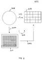
- FIG. 6shows a high-level system diagram 600 that provides a representation of the different modes or paths of transfer of dies from wafers to substrates.
- FIG. 6shows a wafer 400 , a substrate web 608 , and a transfer surface 610 .
- Two pathsare shown in FIG. 6 for transferring dies, a first path 602 , which is a direct path, and a second path 604 , which is a path having intermediate steps.
- first path 602leads directly from wafer 400 to substrate web 608 .
- diescan be transferred from wafer 400 to substrates of substrate web 608 directly, without the dies having first to be transferred from wafer 400 to another surface or storage structure.
- path 604at least two steps are required, path 604 A and path 604 B.
- path 604 Adies are first transferred from wafer 400 to an intermediate transfer surface 610 .
- the diesthen are transferred from transfer surface 610 via path 604 B to the substrates of web 608 .
- Paths 602 and 604each have their advantages.
- path 602can have fewer steps than path 604 , but can have issues of die registration, and other difficulties.
- Path 604typically has a larger number of steps than path 602 , but transfer of dies from wafer 400 to a transfer surface 610 can make die transfer to the substrates of web 808 easier, as die registration may be easier.
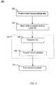
- FIGS. 7 and 8show flowcharts providing steps for transferring dies from a first surface to a second surface, according to embodiments of the present invention. Structural embodiments of the present invention will be apparent to persons skilled in the relevant art(s) based on the following discussion. These steps are described in detail below.
- Flowchart 700begins with step 702 .
- a plurality of dies attached to a support surfaceis received.
- the diesare dies 104 , which are shown attached to a support surface 404 as shown in FIG. 4A .
- support surface 404can be a “green tape” or “blue tape” as would be known to persons skilled in the relevant art(s).
- the plurality of diesare transferred to a subsequent surface.
- dies 104may be transferred by an adhesive tape, a punch tape, a multi-barrel transport mechanism and/or process, die frame, pin plate, such as are further described below and/or in the incorporated patent applications, and may be transferred by other mechanisms and processes, or by combinations of the mechanisms/processes described herein.
- the subsequent surfacecan be an intermediate surface or an actual final substrate.
- the intermediate surfacecan be a transfer surface, including a “blue tape,” as would be known to persons skilled in the relevant art(s).
- the subsequent surfaceis a substrate
- the subsequent surfacemay be a substrate structure that includes a plurality of tag substrates, or may be another substrate type.
- step 706if the subsequent surface is a substrate to which the dies are going to be permanently attached, the process of flowchart 700 is complete. The process can then proceed to step 310 of flowchart 300 , if desired. If the subsequent surface is not a final surface, then the process proceeds to step 704 , where the plurality of dies are then transferred to another subsequent surface. Step 704 may be repeated as many times as is required by the particular application.
- Flowchart 800 of FIG. 8is substantially similar to flowchart of 700 . However, instead of including step 702 , flowchart 800 includes step 802 . In step 802 , a wafer 400 that includes a plurality of dies is received. Thus, in flowchart 800 , a wafer 400 is operated on directly, without being applied to a support surface or structure. Embodiments for both of flowcharts 700 and 800 are described herein.
- any of the intermediate/transfer surfaces and final substrate surfacesmay or may not have cells formed therein for dies to reside therein.
- Various processes described belowmay be used to transfer multiple dies simultaneously between first and second surfaces, according to embodiments of the present invention. In any of the processes described herein, dies may be transferred in either pads-up or pads-down orientations from one surface to another.
- the die transfer processes described hereininclude transfer using an adhesive surface, a parallel die punch process, die plates, including die receptacle structures, pin plates, die transfer heads, and die transfer head coverage patterns. Elements of the die transfer processes described herein may be combined in any way, as would be understood by persons skilled in the relevant art(s). These die transfer processes, and related example structures for performing these processes, are further described in the following subsections.
- diescan be transferred from a wafer or support structure into cells of a die receptacle structure.
- the die receptacle structurehas a plurality of cells, typically arranged in an array of rows and columns of cells, where each cell can hold a die.
- the diescan then be transferred to subsequent intermediate/transfer structures or surfaces, or to a final structure or surface, such as a substrate.
- FIGS. 9A and 9Bshow plan and a cross-sectional views of an example die receptacle structure 900 , according to an embodiment of the present invention.
- die receptacle structure 900comprises a body 902 .
- a plurality of cells 904are formed in a surface of body 902 .
- Cells 904can each hold or contain a die such as a die 104 .
- cells 904are substantially square or rectangular, but cells 904 can have alternative shapes.
- each cell 904has a corresponding opening or hole 906 . While cells 904 are formed in a first surface of body 902 , holes 906 extend all the way through body 902 , being open in a corresponding cell 904 at the first surface and at a second surface of body 902 .
- body 902is substantially square or rectangular in shape, although body 902 can have other shapes.
- body 902can be flat, having a substantially planar shape. Note, however, that body 902 can have any applicable thickness.
- body 902can be made from numerous materials, including a metal or combination of metals/alloy, a plastic, a polymer, glass, a substrate material, other material, and/or any combination thereof.
- holes 906are shown in FIG. 9A as being substantially square or rectangular in shape, holes 906 can have other shapes, including round or elliptical.
- a size or area of a cell 904is greater than a size or diameter of a hole 906 .
- the relative sizes of cell 904 and hole 906can vary from that shown in FIGS. 9A and 9B , where hole 906 has a size much closer to the size of cell 904 .
- a size of hole 906can be much smaller relative to a size of cell 904 .
- Die receptacle structure 900is referred to by other names, including a waffle structure, a waffle grid, and a nest structure or nest plate. Furthermore, die receptacle structure is considered a type of “die plate” that has cells formed therein. Further die plate types, including those which do not have cells formed therein, are described in co-pending application, “Method, System, and Apparatus for Transfer of Dies Using a Die Plate,” U.S. Ser. No. 10/866,253, which is herein incorporated by reference in its entirety.
- a die receptacle structure 900can be formed to hold any number of dies.
- a die receptacle structure 900can be formed to hold a number of dies in the 10s, 100s, 1,000s, 10,000s, or greater numbers of dies.
- cells 904can be referred to by other names.
- cells 904can be referred to as cavities, cubbies, or by other similar names.
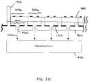
- FIG. 10shows a perspective view of a die receptacle structure 900 , according to an example embodiment of the present invention.
- FIG. 11shows a plurality of dies 104 attached to a support structure 404 (the support structure 404 is shown to be transparent, for illustrative purposes) that is aligned over a die receptacle structure 900 , for die transfer purposes.
- Each die 104 attached to support structure 404is aligned over a corresponding cell 904 of die receptacle structure 900 .
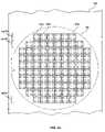
- FIG. 12shows a die receptacle structure 1200 that has all cells 1204 filled with a corresponding die 104 , according to an example embodiment of the present invention.
- a die receptacle structure similar to die receptacle structure shown in FIG. 12could have 135 rows and 270 columns of cells or any other number of rows and columns as required by the particular application.
- die receptacle structure 1200has dimensions of 10.63 inches in the x and y directions and a thickness of 4100 ⁇ m.
- the outermost rows and columns of cells in the example embodiment of die receptacle structure 1200are located 0.5 inches from the outer edges of the structure.
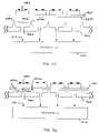
- FIGS. 13A-13Dshow various views of a portion of a die receptacle structure 900 , according to example embodiments of the present invention.
- FIG. 13Ashows an first side cross-sectional view of a die receptacle structure 900 that is filled with dies 104 , showing example dimension values for various dimensions of the example die receptacle structure 900 .
- FIG. 13Bshows a second side cross-sectional view (i.e. die receptacle structure 900 is rotated by 90 degrees) of the die receptacle structure 900 , that is filled with dies 104 , also showing example dimensional values.
- FIG. 13Cshows a perspective view of the die receptacle structure 900 .
- FIG. 13Dshows a die 104 as it would reside in a cell 904 (not shown), with a punch-pin that can be used to move the die 104 out of cell 904 , according to embodiments of the present invention.
- FIGS. 14A and 14Bshow perspective and bottom views, respectively, of a single cell 904 , according to embodiments of the present invention.
- FIG. 14Ashows example dimensional values for various dimensions of the example cell 904 .
- the bottom view of FIG. 14Bshows dimensions of the bottom of the cell 904 , including example dimensions for hole 906 that corresponds to cell 904 .
- die receptacle structure 900is an example of transfer structure 610 shown in FIG. 6 .
- Die receptacle structure 900can be used to transfer dies from a wafer to a substrate, or to another intermediate transfer structure.
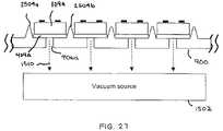
- FIG. 15shows an example die transfer system 1500 that can be used to transfer dies from a wafer 400 to a die receptacle structure 900 , according to an example embodiment of the present invention.
- system 1500can be used to transfer dies along path 604 A, shown in FIG. 6 .
- System 1500includes a wafer 400 , die receptacle structure 900 , and a vacuum source 1502 .
- wafer 400is held in position by a jig or chuck 1504
- die receptacle structure 900is held in position by a jig or chuck 1506 .
- a vacuum source chuck 1508interfaces vacuum source 1502 with a second surface of die receptacle structure 900 .
- Wafer 400is aligned with the first surface of die receptacle structure 900 .
- dies 104 of wafer 400pass from wafer 400 to die receptacle structure 900 due to a suction of vacuum source 1902 .
- vacuum source 1502creates a suction that is directed as shown by arrows 1510 , that moves dies that are separated from wafer 400 into cells 904 of die receptacle structure 900 .
- System 1500may be varied in many ways to transfer dies from wafer 400 , or from a support structure, into die receptacle structure, according to embodiments of the present invention. These embodiments are described in further detail in the following paragraphs.
- FIG. 16shows a flowchart 1600 of a method for transferring die into a die receptacle structure, according to embodiments of the present invention.
- the flowchart depicted in FIG. 16is described with continued reference to FIGS. 9 and 17 - 23 .
- flowchart 1600is not limited to those embodiments. Further operational and structural embodiments of the present invention will be apparent to persons skilled in the relevant arts based on the following discussion. Note that in alternative embodiments, the steps shown in FIG. 16 can occur in an order other than that shown.
- FIG. 17shows an example die receptacle structure 900 , according to an embodiment of the present invention.
- an adhesive materialhas been applied to the first surface of die receptacle structure 900 .
- each of cells 904 in die receptacle structurehave an adhesive material layer 1702 formed therein.
- Adhesive material layer 1702may be any type of adhesive material, including an epoxy, an adhesive tape, or any other adhesive material.
- the wafer 400 and die receptacle structureare positioned to be closely adjacent to each other such that each die of a plurality of dies of the wafer is positioned adjacent to a corresponding cell of a plurality of cells in a first surface of the die receptacle structure.
- FIG. 22shows a wafer 400 positioned relative to die receptacle structure 900 so that each die 104 of wafer 400 is positioned adjacent to a corresponding cell 904 of the plurality of cells 904 in the first surface of die receptacle structure 900 .
- a suctionis applied at a second surface of the die receptacle structure so that at least a partial vacuum exists in each cell of the plurality of cells due to a hole in the second surface corresponding to each cell.
- FIG. 19shows wafer 400 positioned even more closely adjacent to die receptacle structure 900 .
- a vacuum or suctionis shown applied in the direction of arrows 1510 by vacuum source 1502 .
- a saw mechanism 1902is shown in ready position to be applied to wafer 400 .
- Saw mechanism 1902may be any kind of sawing or cutting member, including a saw or other type of blade, a laser, or other cutting or sawing device.
- each die of the plurality of diesis separated from the wafer so that each die is transferred into the corresponding cell of the plurality of cells by the applied suction.
- the separation stepis performed by a saw mechanism.
- FIG. 20shows saw mechanism 1902 being applied to wafer 400 to cut or saw one edge of a die 104 A free from wafer 400 .
- FIG. 21shows saw mechanism 1902 being used to saw a second edge of die 104 A free from wafer 400 .
- vacuum source 1502applies a vacuum or suction in the direction of 1510 , shown in FIG. 21 .
- vacuum source 1502creates at least a partial vacuum in each of cells 904 by directing a vacuum or suction along the direction of arrow 1510 through holes 906 in die receptacle structure 900 .
- diesare separated from the wafer according to FIG. 7 , saw mechanism 1902 , and are transferred into the corresponding cell 904 due to the suction force of vacuum source 1502 .
- FIG. 22shows an example implementation of step 1640 of flowchart 1600 . For example, as shown in FIG.
- die 104 Ahas been transferred or drawn into cell 904 A by vacuum source 1502 through hole 906 A. Furthermore, die 104 A has become attached in cell 904 A due to adhesive material layer 1702 .
- the process of freeing dies 104 from wafer 400can be continued until as many dies as desired have been separated from wafer 400 , and have been transferred into cells 904 of die receptacle structure 900 , including some or all dies 104 of wafer 400 .
- FIG. 23shows a plan view of an example wafer portion of wafer 400 that is held by a jig or chuck 1504 .
- wafer 400has been sawed or cut by sawing mechanism 1902 along an X axis, as shown by X axis cuts 2302 A and 2302 B.
- an Y axis cut 2304is shown being made in wafer 400 .
- Cut 2304has freed die 104 A from wafer 400 .
- die 104 Ais free to transfer into a corresponding cell 904 , assisted by vacuum source 1502 . Cuts through wafer 400 can continue to separate the remaining dies 104 of wafer 400 , and to transfer the dies 104 into corresponding cells 904 of die receptacle structure 900 .
- dies 104can be separated from wafer 400 in a number of ways, including by the parallel use of multiple sawing mechanisms 1902 .
- FIG. 32shows an exemplary system having a positive pressure source and a vacuum/suction source, according to an example embodiment of the present invention.
- positive pressure source 3204exerts a positive pressure on the top surface of wafer 400 .
- the positive pressure source 3204could be a mechanical member that is lowered to contact the top surface of wafer 400 and to apply pressure thereto.
- positive pressure source 3204could provide a punching force through the use of a continuous or burst of air or similar type of pressure.
- the suction/vacuum sourceapplies a negative pressure, described above.
- the positive pressure and vacuummay be applied in an alternating manner. The combination of positive pressure and negative pressure causes dies to transfer from wafer 400 to die receptacle structure 900 .
- dies 104can be transferred from a support surface into die receptacle structure 900 .
- FIG. 24shows a flowchart 2400 of a method for transferring a die from a support structure into a die receptacle structure, according to embodiments of the present invention. The flowchart depicted in FIG. 24 is described with continued reference to FIGS. 9 and 25 - 27 . However, flowchart 2400 is not limited to those embodiments. Further operational and structural embodiments of the present invention will be apparent to persons skilled in the relevant arts based on the following discussion. Note that in alternative embodiments, the steps shown in FIG. 24 can occur in an order other than that shown.
- Flowchart 2400begins in step 2402 when the support structure and die receptacle structure are positioned to be closely adjacent to each other such that each die of a plurality of dies attached to the support structure is positioned adjacent to a corresponding cell of a plurality of cells in a first surface of the die receptacle structure.
- FIG. 25shows an example of step 2402 , where a support structure 404 that attaches dies 104 to a surface thereof is being positioned relative to the first surface of die receptacle structure 900 .
- Each die attached to support structure 404is positioned adjacent to a corresponding cell 904 of die receptacle structure 900 .
- dies 104are attached to support structure 404 and are oriented relative to die receptacle structure 900 , where dies 104 face away from the cells 904 of die receptacle structure 900 .
- dies 104may be positioned on the bottom surface of support structure 404 .
- a suctionis applied at a second surface of the die receptacle structure so that at least a partial vacuum exists in each cell of the plurality of cells due to a hole in the second surface corresponding to each cell.
- vacuum source 1502applies suction, according to step 2404 of flowchart 2400 shown in FIG. 24 .
- support structure 404has come in contact with the top surface of die receptacle structure 900 .
- die receptacle structure 900has been modified.
- the first surface of die receptacle structure 900has sharp edges.
- the edges or portions of die receptacle structure 900 between cells 904are sharp.
- first and second sharp edges 2504 A and 2504are indicated for a first cell 904 A.
- sharp edges 2504are used to separate dies 104 from support structure 2502 .
- support structure 404has an adhesive surface 2502 .
- Surface 2502 of support structure 404is coated with an adhesive material that can be used to adhere dies 104 in cells 904 of die receptacle structure 900 .
- cells 904can have an adhesive material formed therein, similarly to as that described above for FIGS. 17-23 .
- vacuum source 1502applies a suction in the direction of arrows 1510 at a second surface of die receptacle structure 900 .
- at least a partial vacuumexists in each of cells 904 due to the hole 906 that corresponds to each of cells 904 .
- This suctionpulls or forces support structure 404 upon sharp edges 2504 of die receptacle structure 900 .
- step 2406the applied suction is allowed to cause the sharp portions of the die receptacle structure to cut the support structure around each die of the plurality of dies, such that each die of the plurality of dies is separated from the support structure and is transferred into the corresponding cell of the plurality of cells by the applied suction.
- FIG. 27shows an example implementation of step 2406 of flowchart 2400 , shown in FIG. 24 .
- the suction applied by vacuum source 1502is allowed to cause the sharp edges or portions 2504 of die receptacle structure 900 around each die 104 of support structure 404 to cut support structure 404 around each die 104 .
- each die 104is separated from support structure 404 , and is free to remain into the corresponding cell 904 .
- the adhesive bottom surface of support structure 404adheres each die in the respective cell 904 .
- a portion 404 A of support structure 404adheres die 104 A in cell 904 A due to the adhesive material on surface 2502 of portion 404 A.
- FIG. 28shows a flowchart 2800 of a method for transferring a die from a support structure to a die receptacle structure 900 , according to embodiments of the present invention.
- the flowchart depicted in FIG. 24is described with continued reference to FIGS. 9 and 19 - 31 .
- flowchart 2800is not limited to those embodiments. Further operational and structural embodiments of the present invention will be apparent to persons skilled in the relevant arts based on the following discussion.
- FIG. 29shows an example support structure 404 having a plurality of dies 104 attached thereto.
- Dies 104are shown in FIG. 29 attached to the bottom surface of support structure 404 in a die-down or pads-down fashion.
- the contact pads of die 104are on the side of die 104 that is attached to support structure 404 .
- dies 104may be attached to support structure 404 in a pads-up orientation.
- Flowchart 2800begins in step 2802 when the support structure and the die receptacle structure are positioned to be closely adjacent to each other such that each die of a plurality of dies attached to the support structure is positioned in a corresponding cell of a plurality of cells in a first surface of the die receptacle structure.
- FIG. 30shows the bottom surface of support structure 404 positioned to be closely adjacent to die receptacle structure 900 such that each die 104 attached to the bottom surface of support structure 404 is positioned in a corresponding cell 904 of die receptacle structure 900 .
- each die 104attaches to adhesive material layer 1702 that is present in each of cells 904 .
- each die of the plurality of diesis released from the support structure so that each die resides in the corresponding cell of the plurality of cells.
- FIG. 31shows each die 104 of the plurality of dies 104 that were attached to support structure 404 released from support structure 404 .
- each die 104resides in the corresponding cell 904 of the plurality of cells 904 of die receptacle structure 900 .
- Dies 104can be released from support structure 404 in a variety of ways, according to the present invention.
- adhesive material layer 1702may comprise a stronger adhesive force than the adhesive force of support structure 404 .
- support structure 404can be withdrawn of peeled from die receptacle structure 900 , leaving dies 104 attached in their corresponding cells 904 .
- support structure 404can merely be moved away from die receptacle structure 900 to cause dies 104 to be released.
- vacuum or suction of vacuum source 1502can be used to aid in holding dies 104 in cells 904 of die receptacle structure 900 when support structure 404 is moved away.
- vacuum source 1502is optional in the embodiment related to FIGS. 28-31 .
- an adhesive materialmay be additionally applied to the bottom surfaces of dies 104 before positioning dies 104 in cells 904 , instead of, or in addition to, the use of adhesive material layer 1702 in cells 904 .
- FIG. 33shows a flowchart 3300 of a method for recovering untransferred dies using a die receptacle structure, according to embodiments of the present invention.
- the flowchart depicted in FIG. 33is described with continued reference to FIGS. 9 and 34 .
- flowchart 3300is not limited to those embodiments. Further operational and structural embodiments of the present invention will be apparent to persons skilled in the relevant arts based on the following discussion. Note that in alternative embodiments, the steps shown in FIG. 33 can occur in an order other than that shown.
- Flowchart 3300begins at step 3310 when a wafer and, optionally, a first die plate are received.
- the first die platecan be a die receptacle structure, as described above, or a die plate as described in co-pending application, “Method, System, and Apparatus for Transfer of Dies Using a Die Plate,” U.S. Ser. No. 10/866,253.
- step 3320dies are transferred from the wafer to the die plate (or a substrate).
- the diescan be transferred as described herein and in co-pending applications, “Method, System, and Apparatus for Transfer of Dies Using a Die Plate,” U.S. Ser. No. 10/866,253, and “Method, System, and Apparatus for High Volume Transfer of Dies,” U.S. Ser. No. 10/866,149.
- step 3330a determination is made whether any die remain on the wafer following transfer step 3320 . If a determination is made that no dies remain on the wafer, operation proceeds to step 3340 . If a determination is made that dies remain on the wafer (and can be recovered), operation proceeds to step 3350 .
- FIG. 34shows an exemplary wafer 3400 having a plurality of dies remaining after a transfer step is completed.
- dieshave been removed from the center of the wafer. However, dies remain in the periphery of the wafer. For example, as shown in FIG. 34 , dies remain at positions of wafer 3400 labeled 1 - 10 , 17 , 24 , 25 , 32 , and 39 - 48 .
- the arrangement of dies remaining on the wafer after the transfer stepis dependent upon the shape of the die plate to which the dies are transferred and/or upon the method used for transfer. For example, one or more rows or columns of dies may also remain after the transfer.
- step 3340the recovery process for the wafer ends.
- a die receptacle structureis received.
- the die receptacle structuremay be die receptacle structure 900 shown in FIG. 9A , having as many cells (rows/columns) as desired.
- the dies remaining on the waferare transferred to cells 904 in the die receptacle structure 900 .
- This transfercan be via any means including a pin plate, such as described in co-pending application, “Method, System and Apparatus for Transfer of Dies Using a Pin Plate,” U.S. Ser. No. 10/866,159 or via a chip sorter or other similar pick and place technology.
- the pin platemay be designed with a pin configuration to maximize the transfer of the remaining dies.
- the die recovery pin platemay have a different pin configuration (e.g., pins on the periphery but no pins in the central portion) than the die transfer pin plate.
- a pin platecan be designed to have a substantially similar configuration to the configuration of remaining dies.
- all cells in the die receptacle structuremay or may not be filled with a die after completion of the recovery process.
- the resulting die receptacle structurecan then be used as a die plate in the device assembly process.
- the system and method for recovering untransferred dies described abovemay be incorporated into the device assembly system described in co-pending application, “Method, System and Apparatus for Transfer of Dies Using a Pin Plate,” U.S. Ser. No. 10/866,159 or may be a separate system. If it is a separate system, steps 3310 and 3320 are performed by a device assembly system and some or all of steps 3330 through 3360 are performed by the recovery system.
Landscapes
- Engineering & Computer Science (AREA)
- Computer Hardware Design (AREA)
- Microelectronics & Electronic Packaging (AREA)
- Physics & Mathematics (AREA)
- General Physics & Mathematics (AREA)
- Power Engineering (AREA)
- Manufacturing & Machinery (AREA)
- Theoretical Computer Science (AREA)
- Condensed Matter Physics & Semiconductors (AREA)
- Artificial Intelligence (AREA)
- Computer Vision & Pattern Recognition (AREA)
- Container, Conveyance, Adherence, Positioning, Of Wafer (AREA)
- Testing Or Measuring Of Semiconductors Or The Like (AREA)
- Crystals, And After-Treatments Of Crystals (AREA)
- Credit Cards Or The Like (AREA)
- Details Of Aerials (AREA)
- Optical Record Carriers And Manufacture Thereof (AREA)
Abstract
Description
Claims (6)
Priority Applications (1)
| Application Number | Priority Date | Filing Date | Title |
|---|---|---|---|
| US10/866,150US7795076B2 (en) | 2003-06-12 | 2004-06-14 | Method, system, and apparatus for transfer of dies using a die plate having die cavities |
Applications Claiming Priority (2)
| Application Number | Priority Date | Filing Date | Title |
|---|---|---|---|
| US47773503P | 2003-06-12 | 2003-06-12 | |
| US10/866,150US7795076B2 (en) | 2003-06-12 | 2004-06-14 | Method, system, and apparatus for transfer of dies using a die plate having die cavities |
Publications (2)
| Publication Number | Publication Date |
|---|---|
| US20050009232A1 US20050009232A1 (en) | 2005-01-13 |
| US7795076B2true US7795076B2 (en) | 2010-09-14 |
Family
ID=33551754
Family Applications (9)
| Application Number | Title | Priority Date | Filing Date |
|---|---|---|---|
| US10/866,148Expired - Fee RelatedUS7223320B2 (en) | 2003-06-12 | 2004-06-14 | Method and apparatus for expanding a semiconductor wafer |
| US10/866,159AbandonedUS20050015970A1 (en) | 2003-06-12 | 2004-06-14 | Method, system, and apparatus for transfer of dies using a pin plate |
| US10/866,150Expired - LifetimeUS7795076B2 (en) | 2003-06-12 | 2004-06-14 | Method, system, and apparatus for transfer of dies using a die plate having die cavities |
| US10/866,151Expired - LifetimeUS7404199B2 (en) | 2003-06-12 | 2004-06-14 | Method, system, and apparatus for high volume assembly of compact discs and digital video discs incorporating radio frequency identification tag technology |
| US10/866,152Expired - LifetimeUS7276388B2 (en) | 2003-06-12 | 2004-06-14 | Method, system, and apparatus for authenticating devices during assembly |
| US10/866,149AbandonedUS20050005434A1 (en) | 2003-06-12 | 2004-06-14 | Method, system, and apparatus for high volume transfer of dies |
| US10/866,253AbandonedUS20040250417A1 (en) | 2003-06-12 | 2004-06-14 | Method, system, and apparatus for transfer of dies using a die plate |
| US11/393,887Expired - LifetimeUS7543316B2 (en) | 2003-06-12 | 2006-03-31 | Antenna designs for radio frequency identification tags |
| US12/136,565AbandonedUS20080271313A1 (en) | 2003-06-12 | 2008-06-10 | Method, system, and apparatus for transfer of dies using a die plate |
Family Applications Before (2)
| Application Number | Title | Priority Date | Filing Date |
|---|---|---|---|
| US10/866,148Expired - Fee RelatedUS7223320B2 (en) | 2003-06-12 | 2004-06-14 | Method and apparatus for expanding a semiconductor wafer |
| US10/866,159AbandonedUS20050015970A1 (en) | 2003-06-12 | 2004-06-14 | Method, system, and apparatus for transfer of dies using a pin plate |
Family Applications After (6)
| Application Number | Title | Priority Date | Filing Date |
|---|---|---|---|
| US10/866,151Expired - LifetimeUS7404199B2 (en) | 2003-06-12 | 2004-06-14 | Method, system, and apparatus for high volume assembly of compact discs and digital video discs incorporating radio frequency identification tag technology |
| US10/866,152Expired - LifetimeUS7276388B2 (en) | 2003-06-12 | 2004-06-14 | Method, system, and apparatus for authenticating devices during assembly |
| US10/866,149AbandonedUS20050005434A1 (en) | 2003-06-12 | 2004-06-14 | Method, system, and apparatus for high volume transfer of dies |
| US10/866,253AbandonedUS20040250417A1 (en) | 2003-06-12 | 2004-06-14 | Method, system, and apparatus for transfer of dies using a die plate |
| US11/393,887Expired - LifetimeUS7543316B2 (en) | 2003-06-12 | 2006-03-31 | Antenna designs for radio frequency identification tags |
| US12/136,565AbandonedUS20080271313A1 (en) | 2003-06-12 | 2008-06-10 | Method, system, and apparatus for transfer of dies using a die plate |
Country Status (4)
| Country | Link |
|---|---|
| US (9) | US7223320B2 (en) |
| EP (1) | EP1642325A2 (en) |
| TW (1) | TW200504809A (en) |
| WO (1) | WO2004112096A2 (en) |
Cited By (10)
| Publication number | Priority date | Publication date | Assignee | Title |
|---|---|---|---|---|
| US20180122673A1 (en)* | 2016-11-03 | 2018-05-03 | Rohinni, LLC | Compliant Needle for Direct Transfer of Semiconductor Devices |
| US20180138057A1 (en)* | 2015-08-03 | 2018-05-17 | Mikro Mesa Technology Co., Ltd. | Transfer head array |
| US20180261579A1 (en)* | 2015-03-20 | 2018-09-13 | Rohinni, LLC | Method and apparatus for improved direct transfer of semiconductor die |
| US10354895B2 (en) | 2017-01-18 | 2019-07-16 | Rohinni, LLC | Support substrate for transfer of semiconductor devices |
| US10410905B1 (en) | 2018-05-12 | 2019-09-10 | Rohinni, LLC | Method and apparatus for direct transfer of multiple semiconductor devices |
| US10471545B2 (en) | 2016-11-23 | 2019-11-12 | Rohinni, LLC | Top-side laser for direct transfer of semiconductor devices |
| US10504767B2 (en) | 2016-11-23 | 2019-12-10 | Rohinni, LLC | Direct transfer apparatus for a pattern array of semiconductor device die |
| US11094571B2 (en) | 2018-09-28 | 2021-08-17 | Rohinni, LLC | Apparatus to increase transferspeed of semiconductor devices with micro-adjustment |
| TWI753825B (en)* | 2021-05-11 | 2022-01-21 | 財團法人工業技術研究院 | Micro device structure and display apparatus |
| US11488848B2 (en)* | 2018-07-31 | 2022-11-01 | Taiwan Semiconductor Manufacturing Co., Ltd. | Integrated semiconductor die vessel processing workstations |
Families Citing this family (90)
| Publication number | Priority date | Publication date | Assignee | Title |
|---|---|---|---|---|
| US20030130912A1 (en) | 2002-01-04 | 2003-07-10 | Davis Tommy Lee | Equipment management system |
| EP1516325B1 (en)* | 2002-06-14 | 2008-05-14 | Koninklijke Philips Electronics N.V. | Chip on disc record carrier with integrated power supply |
| US6915551B2 (en)* | 2002-08-02 | 2005-07-12 | Matrics, Inc. | Multi-barrel die transfer apparatus and method for transferring dies therewith |
| US7023347B2 (en)* | 2002-08-02 | 2006-04-04 | Symbol Technologies, Inc. | Method and system for forming a die frame and for transferring dies therewith |
| US7443299B2 (en)* | 2003-04-25 | 2008-10-28 | Avery Dennison Corporation | Extended range RFID system |
| US7223320B2 (en)* | 2003-06-12 | 2007-05-29 | Symbol Technologies, Inc. | Method and apparatus for expanding a semiconductor wafer |
| DE602004017840D1 (en)* | 2004-05-17 | 2009-01-02 | Sony Dadc Austria Ag | Optical data carrier, method and device for producing an optical data carrier |
| US7199712B2 (en)* | 2004-06-17 | 2007-04-03 | Tafas Triantafyllos P | System for automatically locating and manipulating positions on an object |
| US20060012387A1 (en)* | 2004-06-29 | 2006-01-19 | Symbol Technologies, Inc. | Systems and methods for testing radio frequency identification tags |
| US20060013680A1 (en)* | 2004-07-16 | 2006-01-19 | Tessera, Inc. | Chip handling methods and apparatus |
| EP1820140A1 (en)* | 2004-12-02 | 2007-08-22 | Sensormatic Electronics Corporation | Radio frequency identification (rfid) device programming system and method |
| US7382254B2 (en)* | 2004-12-03 | 2008-06-03 | Intel Corporation | Storage medium having RFID tag and methods for using same |
| KR20100021665A (en)* | 2004-12-14 | 2010-02-25 | 후지쯔 가부시끼가이샤 | Antenna and noncontact tag |
| US8112326B2 (en)* | 2005-02-03 | 2012-02-07 | TimeSight Systems, Inc. | Inventory management tracking control system |
| US20060236536A1 (en)* | 2005-03-28 | 2006-10-26 | Seiko Epson Corporation | Die apparatus, method for producing perforated work plate, perforated work plate, liquid-jet head and liquid-jet apparatus |
| EP1864266A2 (en)* | 2005-03-29 | 2007-12-12 | Symbol Technologies, Inc. | Smart radio frequency identification (rfid) items |
| US20060225273A1 (en)* | 2005-03-29 | 2006-10-12 | Symbol Technologies, Inc. | Transferring die(s) from an intermediate surface to a substrate |
| US7313037B2 (en)* | 2005-04-21 | 2007-12-25 | Hynix Semiconductor Inc. | RFID system including a memory for correcting a fail cell and method for correcting a fail cell using the same |
| US7364983B2 (en)* | 2005-05-04 | 2008-04-29 | Avery Dennison Corporation | Method and apparatus for creating RFID devices |
| WO2006125206A2 (en)* | 2005-05-19 | 2006-11-23 | Avery Dennison Corporation | Method and apparatus for rfid device assembly |
| WO2007016414A2 (en)* | 2005-07-29 | 2007-02-08 | Flextronics Ap, Llc | Method of aligning the upper and lower centering bells of a lens doublet assembly machine |
| US20070107186A1 (en)* | 2005-11-04 | 2007-05-17 | Symbol Technologies, Inc. | Method and system for high volume transfer of dies to substrates |
| US20070122735A1 (en)* | 2005-11-30 | 2007-05-31 | Wisnudel Marc B | Optical storage device having limited-use content and method for making same |
| US20070131016A1 (en)* | 2005-12-13 | 2007-06-14 | Symbol Technologies, Inc. | Transferring die(s) from an intermediate surface to a substrate |
| US20070139057A1 (en)* | 2005-12-15 | 2007-06-21 | Symbol Technologies, Inc. | System and method for radio frequency identification tag direct connection test |
| KR100716552B1 (en)* | 2006-02-03 | 2007-05-09 | 삼성전자주식회사 | Die attach method |
| US7154283B1 (en)* | 2006-02-22 | 2006-12-26 | Avery Dennison Corporation | Method of determining performance of RFID devices |
| US20070244657A1 (en)* | 2006-04-11 | 2007-10-18 | Drago Randall A | Methods and systems for testing radio frequency identification (RFID) tags having multiple antennas |
| US20070271474A1 (en)* | 2006-05-18 | 2007-11-22 | International Business Machines Corporation | System and method for disabling an electrical device |
| US20070271383A1 (en)* | 2006-05-18 | 2007-11-22 | International Business Machines Corporation | Method and system for managing an electrical device over a power delivery network |
| US7280931B1 (en) | 2006-05-18 | 2007-10-09 | International Business Machines Corporation | Method and system for calibrating an electrical device |
| US20080122119A1 (en)* | 2006-08-31 | 2008-05-29 | Avery Dennison Corporation | Method and apparatus for creating rfid devices using masking techniques |
| US20080085572A1 (en)* | 2006-10-05 | 2008-04-10 | Advanced Chip Engineering Technology Inc. | Semiconductor packaging method by using large panel size |
| KR101058659B1 (en)* | 2006-10-06 | 2011-08-22 | 스미토모 베이클리트 컴퍼니 리미티드 | Semiconductor film, manufacturing method of semiconductor film and semiconductor device |
| US20080103944A1 (en)* | 2006-10-30 | 2008-05-01 | Mobile Logistics Management L.L.C. | Intelligent Pallet |
| US7560303B2 (en)* | 2006-11-07 | 2009-07-14 | Avery Dennison Corporation | Method and apparatus for linear die transfer |
| JP2008235398A (en)* | 2007-03-19 | 2008-10-02 | Disco Abrasive Syst Ltd | Device manufacturing method |
| US8445325B2 (en) | 2007-05-04 | 2013-05-21 | Stats Chippac, Ltd. | Package-in-package using through-hole via die on saw streets |
| US7829998B2 (en) | 2007-05-04 | 2010-11-09 | Stats Chippac, Ltd. | Semiconductor wafer having through-hole vias on saw streets with backside redistribution layer |
| US7723159B2 (en)* | 2007-05-04 | 2010-05-25 | Stats Chippac, Ltd. | Package-on-package using through-hole via die on saw streets |
| US8221244B2 (en) | 2007-08-14 | 2012-07-17 | John B. French | Table with sensors and smart card holder for automated gaming system and gaming cards |
| US8235825B2 (en)* | 2007-08-14 | 2012-08-07 | John B. French | Smart card holder for automated gaming system and gaming cards |
| TWI339865B (en)* | 2007-08-17 | 2011-04-01 | Chipmos Technologies Inc | A dice rearrangement package method |
| US7880614B2 (en)* | 2007-09-26 | 2011-02-01 | Avery Dennison Corporation | RFID interposer with impedance matching |
| SG153683A1 (en)* | 2007-12-14 | 2009-07-29 | Tezzaron Semiconductor S Pte L | 3d integrated circuit package and method of fabrication thereof |
| TWI364801B (en)* | 2007-12-20 | 2012-05-21 | Chipmos Technologies Inc | Dice rearrangement package structure using layout process to form a compliant configuration |
| TWI345276B (en)* | 2007-12-20 | 2011-07-11 | Chipmos Technologies Inc | Dice rearrangement package structure using layout process to form a compliant configuration |
| BRPI0907969A2 (en)* | 2008-02-28 | 2015-08-04 | Ontario Die Internat Inc | System and methods for real-time monitoring of matrix usage or throughput |
| US8077044B2 (en)* | 2008-03-03 | 2011-12-13 | Intermec Ip Corp. | RFID tags with enhanced range and bandwidth obtained by spatial antenna diversity |
| CN101409240B (en)* | 2008-03-21 | 2010-09-08 | 北京德鑫泉科技发展有限公司 | Intelligent label capable of using chip and equipment for producing flip-chip module |
| US8387876B2 (en)* | 2008-05-13 | 2013-03-05 | Nbcuniversal Media, Llc | Activation system and method for activating an optical article |
| US8473974B2 (en)* | 2008-05-13 | 2013-06-25 | Nbcuniversal Media, Llc | Activation system and method for activating an optical article |
| US8488428B2 (en) | 2008-05-14 | 2013-07-16 | Nbcuniversal Media, Llc | Enhanced security of optical article |
| US8034663B2 (en)* | 2008-09-24 | 2011-10-11 | Eastman Kodak Company | Low cost die release wafer |
| US7879691B2 (en)* | 2008-09-24 | 2011-02-01 | Eastman Kodak Company | Low cost die placement |
| US8361840B2 (en)* | 2008-09-24 | 2013-01-29 | Eastman Kodak Company | Thermal barrier layer for integrated circuit manufacture |
| US7772042B2 (en)* | 2008-09-24 | 2010-08-10 | Eastman Kodak Company | Solvent softening to allow die placement |
| US20100072490A1 (en)* | 2008-09-24 | 2010-03-25 | Kerr Roger S | Low cost flexible display sheet |
| US8062507B2 (en)* | 2008-09-25 | 2011-11-22 | Uop Llc | Stripping process with multi-sloped baffles |
| EP2296149A1 (en)* | 2009-05-27 | 2011-03-16 | Nxp B.V. | Apparatus for storing digital media that includes a radio frequency identification system |
| FR2962646B1 (en) | 2010-07-16 | 2012-06-22 | Sofradim Production | PROSTHETIC WITH RADIO OPAQUE ELEMENT |
| JP5637759B2 (en)* | 2010-07-27 | 2014-12-10 | 日本発條株式会社 | Method for tearing plate material, plate material, and apparatus |
| US9861590B2 (en) | 2010-10-19 | 2018-01-09 | Covidien Lp | Self-supporting films for delivery of therapeutic agents |
| US8877523B2 (en) | 2011-06-22 | 2014-11-04 | Freescale Semiconductor, Inc. | Recovery method for poor yield at integrated circuit die panelization |
| FR2977790B1 (en) | 2011-07-13 | 2013-07-19 | Sofradim Production | PROSTHETIC FOR UMBILIC HERNIA |
| CN103064248A (en)* | 2011-10-21 | 2013-04-24 | 联胜(中国)科技有限公司 | Fabrication method of thin film pattern and substrate structure |
| US9005308B2 (en) | 2011-10-25 | 2015-04-14 | Covidien Lp | Implantable film/mesh composite for passage of tissue therebetween |
| US10206769B2 (en) | 2012-03-30 | 2019-02-19 | Covidien Lp | Implantable devices including a film providing folding characteristics |
| FR2992662B1 (en) | 2012-06-28 | 2014-08-08 | Sofradim Production | KNIT WITH PICOTS |
| FR2992547B1 (en) | 2012-06-29 | 2015-04-24 | Sofradim Production | PROSTHETIC FOR HERNIA |
| CN103579069A (en)* | 2012-07-20 | 2014-02-12 | 久元电子股份有限公司 | Die pick-and-place method, die pick-and-place bearing structure, and die pick-and-place device |
| CN103794517A (en)* | 2012-11-01 | 2014-05-14 | 威控自动化机械股份有限公司 | Round Die Placement Method |
| US9583363B2 (en) | 2012-12-31 | 2017-02-28 | Sunedison Semiconductor Limited (Uen201334164H) | Processes and apparatus for preparing heterostructures with reduced strain by radial distension |
| JP5956944B2 (en)* | 2013-02-28 | 2016-07-27 | 日本電産サンキョー株式会社 | Non-contact information processing device |
| US9193525B2 (en)* | 2014-03-12 | 2015-11-24 | Asm Technology Singapore Pte Ltd | Apparatus for handling electronic components |
| DE102014111744B4 (en)* | 2014-08-18 | 2022-01-05 | Infineon Technologies Ag | ASSEMBLY FOR HANDLING A SEMICONDUCTOR CHIP AND METHOD OF HANDLING A SEMICONDUCTOR CHIP |
| WO2017052534A1 (en)* | 2015-09-23 | 2017-03-30 | Brun Xavier | Method of manufacturing ultra thin wafers |
| CN107134427B (en)* | 2016-02-29 | 2020-05-01 | 上海微电子装备(集团)股份有限公司 | Chip bonding apparatus and method |
| JP6656026B2 (en)* | 2016-03-08 | 2020-03-04 | キヤノン株式会社 | Information processing apparatus, information processing control method, and computer program |
| US10429438B1 (en)* | 2016-07-28 | 2019-10-01 | National Technology & Engineering Solutions Of Sandia, Llc | Integrated circuit authentication from a die material measurement |
| US10297478B2 (en)* | 2016-11-23 | 2019-05-21 | Rohinni, LLC | Method and apparatus for embedding semiconductor devices |
| GB2559780B (en)* | 2017-02-17 | 2019-05-15 | Nu Nano Ltd | Passive semiconductor device assembly technology |
| CN109465628B (en)* | 2018-11-29 | 2020-07-24 | 重庆市璧山区昌瑞电子有限公司 | Assembling and pressing jig and pressing method for exhaust screw and screw plug cap |
| CN109714701B (en)* | 2018-12-11 | 2020-12-01 | 深圳市联智物联网科技有限公司 | Airport luggage management system |
| CN109530162B (en)* | 2018-12-27 | 2020-08-14 | 杭州小橙工业设计有限公司 | An LED processing system |
| CN114270508A (en)* | 2019-08-23 | 2022-04-01 | 塞尔法雷公司 | Method and system for stretching receptor substrates to adjust arrangement of components |
| JP7330873B2 (en)* | 2019-12-10 | 2023-08-22 | 日本発條株式会社 | Plate material, method for tearing off plate material, and suspension |
| KR102321368B1 (en)* | 2019-12-17 | 2021-11-03 | 한국광기술원 | Laser Light Package with Uniform Alignment and Method for Manufacturing thereof |
| TW202201592A (en)* | 2020-06-15 | 2022-01-01 | 賢昇科技股份有限公司 | Equipment and method for transferring workpieces including a carrying apparatus, a pressing apparatus, a peeling apparatus and a controlling apparatus |
| US11889742B2 (en)* | 2020-11-04 | 2024-01-30 | Samsung Display Co., Ltd. | Apparatus of manufacturing display device and method of manufacturing display device |
Citations (148)
| Publication number | Priority date | Publication date | Assignee | Title |
|---|---|---|---|---|
| US2782487A (en) | 1950-05-12 | 1957-02-26 | Properzi Ilario | Device for making metal pellets, particularly for shotguns |
| US3010427A (en) | 1959-12-14 | 1961-11-28 | Llewellyn A Hautau | Adhesive dispensing machine |
| US3724737A (en) | 1971-10-06 | 1973-04-03 | E Bodnar | Spreader for slit web material |
| US3891157A (en) | 1973-06-04 | 1975-06-24 | Beloit Corp | Slitting mechanism for winder |
| US3989575A (en) | 1975-04-16 | 1976-11-02 | Oliver Machinery Company | Split labeling apparatus |
| US4040169A (en) | 1974-03-04 | 1977-08-09 | Watkins-Johnson Co. | Method of fabricating an array of semiconductor devices |
| US4231153A (en) | 1979-02-22 | 1980-11-04 | Browne Lawrence T | Article placement system |
| US4298120A (en)* | 1978-12-26 | 1981-11-03 | Murata Manufacturing Co., Ltd. | Chip-like electronic component series and method for supplying chip-like electronic components |
| US4342090A (en) | 1980-06-27 | 1982-07-27 | International Business Machines Corp. | Batch chip placement system |
| US4451324A (en) | 1979-05-12 | 1984-05-29 | Sony Corporation | Apparatus for placing chip type circuit elements on a board |
| US4452557A (en) | 1980-11-13 | 1984-06-05 | U.S. Philips Corporation | Device for the simultaneous positioning of a plurality of electrical and/or electronic parts on a printed circuit board |
| US4480742A (en) | 1981-07-02 | 1984-11-06 | Agfa-Gevaert N.V. | Method and apparatus for conveying and spreading material |
| US4914809A (en) | 1988-02-15 | 1990-04-10 | Taiyo Yuden Co., Ltd. | Chip mounting apparatus |
| US4925808A (en) | 1989-03-24 | 1990-05-15 | Sprague Electric Company | Method for making IC die with dielectric isolation |
| US4953283A (en) | 1987-11-28 | 1990-09-04 | Murata Manufacturing Co., Ltd. | Method of handling electronic component chips |
| US4965927A (en) | 1989-09-21 | 1990-10-30 | Eli Holzman | Apparatus for applying surface-mounted electronic components to printed circuit boards |
| US5147210A (en) | 1988-03-03 | 1992-09-15 | Western Digital Corporation | Polymer film interconnect |
| US5256578A (en) | 1991-12-23 | 1993-10-26 | Motorola, Inc. | Integral semiconductor wafer map recording |
| US5255430A (en) | 1992-10-08 | 1993-10-26 | Atmel Corporation | Method of assembling a module for a smart card |
| US5510723A (en) | 1994-03-01 | 1996-04-23 | Micron Custom Manufacturing, Inc. Usa | Diced semiconductor device handler |
| US5519381A (en) | 1992-11-18 | 1996-05-21 | British Technology Group Limited | Detection of multiple articles |
| US5528222A (en) | 1994-09-09 | 1996-06-18 | International Business Machines Corporation | Radio frequency circuit and memory in thin flexible package |
| US5537105A (en) | 1991-01-04 | 1996-07-16 | British Technology Group Limited | Electronic identification system |
| US5557280A (en) | 1992-08-26 | 1996-09-17 | British Technology Group Limited | Synchronized electronic identification system |
| US5564888A (en) | 1993-09-27 | 1996-10-15 | Doan; Carl V. | Pick and place machine |
| US5566441A (en) | 1993-03-11 | 1996-10-22 | British Technology Group Limited | Attaching an electronic circuit to a substrate |
| US5585193A (en) | 1993-07-16 | 1996-12-17 | Avery Dennison Corporation | Machine-direction oriented label films and die-cut labels prepared therefrom |
| US5616759A (en) | 1991-05-28 | 1997-04-01 | Wisconsin Alumni Research Foundation | Cyclohexylidene compounds |
| US5618759A (en) | 1995-05-31 | 1997-04-08 | Texas Instruments Incorporated | Methods of and apparatus for immobilizing semiconductor wafers during sawing thereof |
| US5725728A (en) | 1995-09-18 | 1998-03-10 | Kabushiki Kaisha Shinkawa | Pellet pick-up device |
| US5827394A (en) | 1996-07-15 | 1998-10-27 | Vanguard International Semiconductor Corporation | Step and repeat exposure method for loosening integrated circuit dice from a radiation sensitive adhesive tape backing |
| US5837349A (en) | 1992-10-09 | 1998-11-17 | Illinois Tool Works Inc. | Method and apparatus for producing oriented plastic strap, and strap produced thereby |
| US5840594A (en)* | 1996-09-27 | 1998-11-24 | Matsushita Electric Industrial Co., Ltd. | Method of and apparatus for mounting electronic parts on a board |
| US5862117A (en) | 1997-03-12 | 1999-01-19 | Em Microelectronic-Marin Sa | Device, in particular a compact disc, comprising a data storage medium and an integrated circuit |
| US5880934A (en) | 1994-05-11 | 1999-03-09 | Giesecke & Devrient Gmbh | Data carrier having separately provided integrated circuit and induction coil |
| US5904546A (en) | 1996-02-12 | 1999-05-18 | Micron Technology, Inc. | Method and apparatus for dicing semiconductor wafers |
| US5911456A (en)* | 1996-09-27 | 1999-06-15 | Matsushita Electric Industrial Co., Ltd. | Method and apparatus for mounting parts with pick-up mistake detection and storage of mistake rate |
| US5946198A (en) | 1994-10-21 | 1999-08-31 | Giesecke & Devrient Gmbh | Contactless electronic module with self-supporting metal coil |
| US5953590A (en) | 1996-11-26 | 1999-09-14 | Micron Technology, Inc. | Method and apparatus to hold integrated circuit chips onto a chuck and to simultaneously remove multiple integrated circuit chips from a cutting chuck |
| US5966903A (en) | 1998-05-27 | 1999-10-19 | Lucent Technologies Inc. | High speed flip-chip dispensing |
| US5976306A (en) | 1998-02-18 | 1999-11-02 | Hover-Davis, Inc. | Method and apparatus for removing die from an expanded wafer and conveying die to a pickup location |
| US5982284A (en) | 1997-09-19 | 1999-11-09 | Avery Dennison Corporation | Tag or label with laminated thin, flat, flexible device |
| US6002344A (en) | 1997-11-21 | 1999-12-14 | Bandy; William R. | System and method for electronic inventory |
| US6018299A (en) | 1998-06-09 | 2000-01-25 | Motorola, Inc. | Radio frequency identification tag having a printed antenna and method |
| US6027027A (en) | 1996-05-31 | 2000-02-22 | Lucent Technologies Inc. | Luggage tag assembly |
| DE19840226A1 (en) | 1998-09-03 | 2000-03-16 | Fraunhofer Ges Forschung | Method of applying a circuit chip to a carrier |
| WO2000014733A1 (en) | 1998-09-02 | 2000-03-16 | Hitachi, Ltd. | Information recording/reproducing device |
| US6044046A (en) | 1996-04-26 | 2000-03-28 | Giesecke & Devrient Gmbh | CD with built-in chip |
| US6082660A (en) | 1996-06-14 | 2000-07-04 | Beloit Technologies, Inc. | Separating device for winding devices for material webs, longitudinally divided into several partial webs |
| US6091332A (en) | 1998-06-09 | 2000-07-18 | Motorola, Inc. | Radio frequency identification tag having printed circuit interconnections |
| US6107920A (en) | 1998-06-09 | 2000-08-22 | Motorola, Inc. | Radio frequency identification tag having an article integrated antenna |
| US6121118A (en) | 1998-11-30 | 2000-09-19 | Samsung Electronics Co., Ltd. | Chip separation device and method |
| US6135522A (en) | 1999-05-26 | 2000-10-24 | Advanced Semiconductors Engineering, Inc. | Sucker for transferring packaged semiconductor device |
| US6145901A (en) | 1996-03-11 | 2000-11-14 | Rich; Donald S. | Pick and place head construction |
| US6147662A (en) | 1999-09-10 | 2000-11-14 | Moore North America, Inc. | Radio frequency identification tags and labels |
| US6165386A (en) | 1998-09-30 | 2000-12-26 | Toppan Forms Co., Ltd. | Photosetting conductive paste |
| US6169319B1 (en) | 1999-08-12 | 2001-01-02 | Tower Semiconductor Ltd. | Backside illuminated image sensor |
| US6173750B1 (en) | 1998-02-18 | 2001-01-16 | Hover-Davis, Inc. | Method and apparatus for removing die from a wafer and conveying die to a pickup location |
| US6189591B1 (en) | 1997-11-19 | 2001-02-20 | Shibaura Mechatronics Corporation | Wafer sheet expanding apparatus and pellet bonding apparatus using thereof |
| US6204092B1 (en)* | 1999-04-13 | 2001-03-20 | Lucent Technologies, Inc. | Apparatus and method for transferring semiconductor die to a carrier |
| US6202292B1 (en) | 1998-08-26 | 2001-03-20 | Micron Technology, Inc. | Apparatus for removing carrier film from a semiconductor die |
| US6206292B1 (en) | 1999-01-23 | 2001-03-27 | Sihl Gmbh | Surface-printable RFID-transponders |
| US6205745B1 (en) | 1998-05-27 | 2001-03-27 | Lucent Technologies Inc. | High speed flip-chip dispensing |
| US6215194B1 (en) | 1998-10-01 | 2001-04-10 | Mitsubishi Denki Kabushiki Kaisha | Wafer sheet with adhesive on both sides and attached semiconductor wafer |
| US6226109B1 (en) | 1998-08-10 | 2001-05-01 | Ovd Kinegram Ag | Diffractive security device on compact discs |
| JP2001127415A (en) | 1999-10-29 | 2001-05-11 | Toppan Forms Co Ltd | IC chip mounting method |
| US6248199B1 (en) | 1999-04-26 | 2001-06-19 | Soundcraft, Inc. | Method for the continuous fabrication of access control and identification cards with embedded electronics or other elements |
| US6248201B1 (en) | 1999-05-14 | 2001-06-19 | Lucent Technologies, Inc. | Apparatus and method for chip processing |
| US6262692B1 (en) | 1999-01-13 | 2001-07-17 | Brady Worldwide, Inc. | Laminate RFID label and method of manufacture |
| US6265977B1 (en) | 1998-09-11 | 2001-07-24 | Motorola, Inc. | Radio frequency identification tag apparatus and related method |
| WO2001054058A1 (en) | 2000-01-17 | 2001-07-26 | Rafsec Oy | Method to manufacture a smart label inlet web and a smart label inlet web |
| US20010014524A1 (en) | 1999-02-19 | 2001-08-16 | Paul A. Farrar | Selective deposition of solder ball contacts |
| WO2001061646A1 (en) | 2000-02-18 | 2001-08-23 | Moore North America, Inc. | Rfid manufacturing concepts |
| US20010016400A1 (en) | 2000-02-21 | 2001-08-23 | Chun-Chi Lee | Method of making wafer level chip scale package |
| US6281795B1 (en) | 2000-02-08 | 2001-08-28 | Moore North America, Inc. | RFID or EAS label mount with double sided tape |
| US6283693B1 (en)* | 1999-11-12 | 2001-09-04 | General Semiconductor, Inc. | Method and apparatus for semiconductor chip handling |
| US6283703B1 (en) | 1999-10-22 | 2001-09-04 | Laurier Incorporated | Automatic conveying apparatus for JEDEC carrier members |
| JP2001257222A (en) | 2000-03-09 | 2001-09-21 | Hitachi Ltd | Semiconductor mounting device and method of manufacturing the same |
| US6303462B1 (en) | 1998-08-25 | 2001-10-16 | Commissariat A L'energie Atomique | Process for physical isolation of regions of a substrate board |
| US6303468B1 (en) | 1997-08-12 | 2001-10-16 | Commissariat A L'energie Atomique | Method for making a thin film of solid material |
| WO2001076949A2 (en) | 2000-04-07 | 2001-10-18 | Melzer Maschinenbau Gmbh | Method and device for producing data carriers equipped with an integrated transponder |
| US6322903B1 (en) | 1999-12-06 | 2001-11-27 | Tru-Si Technologies, Inc. | Package of integrated circuits and vertical integration |
| WO2001095241A1 (en) | 2000-06-06 | 2001-12-13 | Rafsec Oy | A method and an apparatus for manufacturing a smart label inlet web |
| US6331225B1 (en) | 1997-05-16 | 2001-12-18 | Sony Corporation | Apparatus and method for mounting electronic parts |
| US20020020491A1 (en) | 2000-04-04 | 2002-02-21 | Price David M. | High speed flip chip assembly process |
| US6359842B1 (en) | 1998-10-22 | 2002-03-19 | Hitachi, Ltd. | Disc having a semiconductor memory |
| US6370750B1 (en)* | 1998-10-27 | 2002-04-16 | Matsushita Electric Industrial Co., Ltd. | Component affixing method and apparatus |
| US20020050591A1 (en) | 1999-04-15 | 2002-05-02 | Tandy Patrick W. | Apparatus and method for marking defective sections of laminate substrates |
| WO2002037414A1 (en) | 2000-11-01 | 2002-05-10 | Rafsec Oy | A method for the manufacture of a smart label, and a smart label |
| DE19805031C2 (en) | 1998-02-09 | 2002-06-13 | Peter Kammer | Method and device for producing chip cards |
| WO2002049093A1 (en) | 2000-12-11 | 2002-06-20 | Rafsec Oy | A smart label web and a method for its manufacture |
| US20020081772A1 (en)* | 2000-12-21 | 2002-06-27 | Madrid Ruben P. | Method and system for manufacturing ball grid array ("BGA") packages |
| JP2002190003A (en) | 2000-12-21 | 2002-07-05 | Hitachi Ltd | IC module manufacturing method |
| US6416608B1 (en) | 1997-05-28 | 2002-07-09 | Avery Denison Corporation | Method for producing a multi-layer label and device for implementing said method |
| WO2002082368A1 (en) | 2001-04-06 | 2002-10-17 | Rafsec Oy | A smart card web and a method for its manufacture |
| US6483174B1 (en)* | 2001-08-16 | 2002-11-19 | Jds Uniphase Corporation | Apparatus and method for dicing and testing optical devices, including thin film filters |
| JP2002373917A (en) | 2001-06-15 | 2002-12-26 | Hitachi Ltd | Semiconductor device and manufacturing method thereof |
| US6514790B1 (en) | 1998-09-03 | 2003-02-04 | Fraunhofer-Gesellschaft Zur Foerderung Der Angewandten Forschung E.V. | Method for handling a plurality of circuit chips |
| US20030024635A1 (en) | 2001-07-24 | 2003-02-06 | Seiko Epson Corporation | Method for transferring element, method for producing element, integrated circuit, circuit board, electro-optical device, IC card, and electronic appliance |
| FR2775533B1 (en) | 1998-02-27 | 2003-02-14 | Gemplus Sca | ELECTRONIC DEVICE WITH NON-CONTACT ELECTRONIC MEMORY, AND METHOD FOR MANUFACTURING SUCH A DEVICE |
| US6521511B1 (en) | 1997-07-03 | 2003-02-18 | Seiko Epson Corporation | Thin film device transfer method, thin film device, thin film integrated circuit device, active matrix board, liquid crystal display, and electronic apparatus |
| US6534386B2 (en) | 2001-06-26 | 2003-03-18 | Mitsubishi Denki Kabushiki Kaisha | Method of manufacturing semiconductor chips |
| US6554128B1 (en) | 1999-10-07 | 2003-04-29 | Delaware Capital Formation, Inc. | Die shuttle conveyor and nest therefor |
| US6555400B2 (en) | 2001-08-22 | 2003-04-29 | Micron Technology, Inc. | Method for substrate mapping |
| US20030089970A1 (en) | 2001-11-09 | 2003-05-15 | Gates Tim M. | Semiconductor package having multi-signal bus bars |
| DE19634473C2 (en) | 1996-07-11 | 2003-06-26 | David Finn | Process for the production of a chip card |
| US20030136503A1 (en) | 2002-01-18 | 2003-07-24 | Avery Dennison Corporation | RFID label technique |
| US20030140476A1 (en) | 2002-01-31 | 2003-07-31 | Barretto Anthony A. | Substrate alignment method and apparatus |
| US6606247B2 (en) | 2001-05-31 | 2003-08-12 | Alien Technology Corporation | Multi-feature-size electronic structures |
| US6608370B1 (en) | 2002-01-28 | 2003-08-19 | Motorola, Inc. | Semiconductor wafer having a thin die and tethers and methods of making the same |
| US6617963B1 (en) | 1999-02-26 | 2003-09-09 | Sri International | Event-recording devices with identification codes |
| US20030197653A1 (en) | 2002-04-22 | 2003-10-23 | Russell Barber | RFID antenna apparatus and system |
| US20030211652A1 (en) | 2002-05-07 | 2003-11-13 | Michael Summers | Method and apparatus for the multiplexed acquisition of a bar die from a wafer |
| US20030217805A1 (en) | 2002-05-17 | 2003-11-27 | Semiconductor Energy Laboratory Co. , Ltd. | Method of transferring a laminate and method of manufacturig a semiconductor device |
| US20030224248A1 (en)* | 2002-06-04 | 2003-12-04 | Tulip Corporation | Cold formed battery terminal |
| US20030231107A1 (en) | 2002-04-08 | 2003-12-18 | Edmonson Peter J. | Dual track surface acoustic wave RFID/sensor |
| KR20040009803A (en)* | 2002-07-25 | 2004-01-31 | 삼성전자주식회사 | Pick and place apparatus for semiconductor chip package that vacuum pad pitch setting is free |
| US20040020040A1 (en)* | 2002-08-02 | 2004-02-05 | Matrics, Inc. | Method and system for forming a die frame for transferring dies therewith |
| US20040020038A1 (en)* | 2002-08-02 | 2004-02-05 | Matrics, Inc. | System and method of transferring dies using an adhesive surface |
| US6692978B2 (en) | 2000-08-25 | 2004-02-17 | Micron Technology, Inc. | Methods for marking a bare semiconductor die |
| US20040037061A1 (en) | 2002-08-21 | 2004-02-26 | David Liu | Method and components for manufacturing multi-layer modular electrical circuits |
| US20040052202A1 (en) | 2002-09-13 | 2004-03-18 | Brollier Brian W. | RFID enabled information disks |
| US20040054594A1 (en) | 2002-09-12 | 2004-03-18 | Forster Ian J. | RFID security device for optical disc |
| US20040072385A1 (en)* | 2002-10-15 | 2004-04-15 | Bauer Donald G. | Chip alignment and placement apparatus for integrated circuit, mems, photonic or other devices |
| US6731353B1 (en) | 2001-08-17 | 2004-05-04 | Alien Technology Corporation | Method and apparatus for transferring blocks |
| US20040118512A1 (en)* | 2002-12-20 | 2004-06-24 | Norbert Hiller | Systems for assembling components on submounts and methods therefor |
| US20040125040A1 (en) | 2002-12-31 | 2004-07-01 | Ferguson Scott Wayne | RFID device and method of forming |
| US6780672B2 (en) | 2000-01-31 | 2004-08-24 | Lockheed Martin Corporation | Micro eletro-mechanical component and system architecture |
| US20040192011A1 (en) | 2003-03-25 | 2004-09-30 | Bruce Roesner | Chip attachment in an RFID tag |
| US20040203185A1 (en) | 2003-04-11 | 2004-10-14 | Eastman Kodak Company | Medium having data storage and communication capabilities and method for forming same |
| US20040217865A1 (en) | 2002-03-01 | 2004-11-04 | Turner Christopher G.G. | RFID tag |
| US20040250949A1 (en) | 2003-06-12 | 2004-12-16 | Matrics, Inc. | Method and apparatus for expanding a semiconductor wafer |
| US20050026315A1 (en) | 2002-06-20 | 2005-02-03 | Micron Technology, Inc. | Isolation circuit |
| US20050040994A1 (en) | 2003-08-22 | 2005-02-24 | Checkpoint Systems, Inc. | Security tag with three dimensional antenna array made from flat stock |
| US6868800B2 (en) | 2001-09-28 | 2005-03-22 | Tokyo Electron Limited | Branching RF antennas and plasma processing apparatus |
| US6879029B2 (en) | 1999-11-17 | 2005-04-12 | Denso Corporation | Semiconductor device having element isolation structure |
| US6891515B1 (en) | 1999-06-10 | 2005-05-10 | Harada Industry Co., Ltd. | Multiband antenna |
| US20050176170A1 (en) | 2001-03-02 | 2005-08-11 | Detig Robert H. | Process for the manufacture of large area arrays of discrete components |
| US7060593B2 (en)* | 2001-09-27 | 2006-06-13 | Kabushiki Kaisha Toshiba | Method of and mechanism for peeling adhesive tape bonded to segmented semiconductor wafer |
| US7075436B2 (en) | 2001-02-12 | 2006-07-11 | Symbol Technologies, Inc. | Method, system, and apparatus for binary traversal of a tag population |
| US7086073B2 (en) | 2003-06-16 | 2006-08-01 | Microsoft Corporation | Optical storage media with embedded security device |
| US7102526B2 (en) | 2003-04-25 | 2006-09-05 | Stephen Eliot Zweig | Electronic time-temperature indicator and logger |
| US20060225273A1 (en) | 2005-03-29 | 2006-10-12 | Symbol Technologies, Inc. | Transferring die(s) from an intermediate surface to a substrate |
| US20070040689A1 (en) | 2005-08-19 | 2007-02-22 | Thingmagic, Inc. | Dynamically reconfigurable antennas for RFID label encoders/readers |
| US20070107186A1 (en) | 2005-11-04 | 2007-05-17 | Symbol Technologies, Inc. | Method and system for high volume transfer of dies to substrates |
| US20070152901A1 (en) | 2006-02-10 | 2007-07-05 | Symbol Technologies, Inc. | Antenna designs for radio frequency identification (RFID) tags |
| US7363642B2 (en) | 2002-08-09 | 2008-04-22 | Matsushita Electric Industrial Co., Ltd. | Optical disc and remote control device |
| US7378971B2 (en) | 2004-10-01 | 2008-05-27 | Hitachi America, Ltd. | Radio frequency identification tags for digital storage discs |
Family Cites Families (8)
| Publication number | Priority date | Publication date | Assignee | Title |
|---|---|---|---|---|
| JPS55118690A (en) | 1979-03-05 | 1980-09-11 | Matsushita Electric Industrial Co Ltd | Device for carrying electronic part |
| US4925806A (en)* | 1988-03-17 | 1990-05-15 | Northern Telecom Limited | Method for making a doped well in a semiconductor substrate |
| US5731353A (en)* | 1993-09-08 | 1998-03-24 | Ajinomoto Co., Inc. | Stilbene derivatives and pharmaceutical compositions containing them |
| US6282692B1 (en)* | 1998-12-03 | 2001-08-28 | International Business Machines Corporation | Structure for improved capacitance and inductance calculation |
| US6332903B1 (en)* | 2000-08-04 | 2001-12-25 | Tony U. Otani | Materials processing cylinder containing titanium carbide |
| JP2004509479A (en)* | 2000-09-19 | 2004-03-25 | ナノピアス・テクノロジーズ・インコーポレイテッド | Method for assembling a plurality of components and a plurality of antennas in a radio frequency identification device |
| CA2494487A1 (en)* | 2002-08-02 | 2004-02-12 | Symbol Technologies, Inc. | Method and apparatus for high volume assembly of radio frequency identification tags |
| US6976306B1 (en)* | 2004-07-12 | 2005-12-20 | Unitech Printed Circuit Board Corporation | Modular method for manufacturing circuit board |
- 2004
- 2004-06-14USUS10/866,148patent/US7223320B2/ennot_activeExpired - Fee Related
- 2004-06-14USUS10/866,159patent/US20050015970A1/ennot_activeAbandoned
- 2004-06-14WOPCT/US2004/018577patent/WO2004112096A2/enactiveApplication Filing
- 2004-06-14EPEP04754983Apatent/EP1642325A2/ennot_activeWithdrawn
- 2004-06-14USUS10/866,150patent/US7795076B2/ennot_activeExpired - Lifetime
- 2004-06-14USUS10/866,151patent/US7404199B2/ennot_activeExpired - Lifetime
- 2004-06-14USUS10/866,152patent/US7276388B2/ennot_activeExpired - Lifetime
- 2004-06-14USUS10/866,149patent/US20050005434A1/ennot_activeAbandoned
- 2004-06-14TWTW093117078Apatent/TW200504809A/enunknown
- 2004-06-14USUS10/866,253patent/US20040250417A1/ennot_activeAbandoned
- 2006
- 2006-03-31USUS11/393,887patent/US7543316B2/ennot_activeExpired - Lifetime
- 2008
- 2008-06-10USUS12/136,565patent/US20080271313A1/ennot_activeAbandoned
Patent Citations (172)
| Publication number | Priority date | Publication date | Assignee | Title |
|---|---|---|---|---|
| US2782487A (en) | 1950-05-12 | 1957-02-26 | Properzi Ilario | Device for making metal pellets, particularly for shotguns |
| US3010427A (en) | 1959-12-14 | 1961-11-28 | Llewellyn A Hautau | Adhesive dispensing machine |
| US3724737A (en) | 1971-10-06 | 1973-04-03 | E Bodnar | Spreader for slit web material |
| US3891157A (en) | 1973-06-04 | 1975-06-24 | Beloit Corp | Slitting mechanism for winder |
| US4040169A (en) | 1974-03-04 | 1977-08-09 | Watkins-Johnson Co. | Method of fabricating an array of semiconductor devices |
| US3989575A (en) | 1975-04-16 | 1976-11-02 | Oliver Machinery Company | Split labeling apparatus |
| US4298120A (en)* | 1978-12-26 | 1981-11-03 | Murata Manufacturing Co., Ltd. | Chip-like electronic component series and method for supplying chip-like electronic components |
| US4231153A (en) | 1979-02-22 | 1980-11-04 | Browne Lawrence T | Article placement system |
| US4451324A (en) | 1979-05-12 | 1984-05-29 | Sony Corporation | Apparatus for placing chip type circuit elements on a board |
| US4342090A (en) | 1980-06-27 | 1982-07-27 | International Business Machines Corp. | Batch chip placement system |
| US4452557A (en) | 1980-11-13 | 1984-06-05 | U.S. Philips Corporation | Device for the simultaneous positioning of a plurality of electrical and/or electronic parts on a printed circuit board |
| US4480742A (en) | 1981-07-02 | 1984-11-06 | Agfa-Gevaert N.V. | Method and apparatus for conveying and spreading material |
| US4953283A (en) | 1987-11-28 | 1990-09-04 | Murata Manufacturing Co., Ltd. | Method of handling electronic component chips |
| US4914809A (en) | 1988-02-15 | 1990-04-10 | Taiyo Yuden Co., Ltd. | Chip mounting apparatus |
| US5147210A (en) | 1988-03-03 | 1992-09-15 | Western Digital Corporation | Polymer film interconnect |
| US4925808A (en) | 1989-03-24 | 1990-05-15 | Sprague Electric Company | Method for making IC die with dielectric isolation |
| US4965927A (en) | 1989-09-21 | 1990-10-30 | Eli Holzman | Apparatus for applying surface-mounted electronic components to printed circuit boards |
| US5537105A (en) | 1991-01-04 | 1996-07-16 | British Technology Group Limited | Electronic identification system |
| US5616759A (en) | 1991-05-28 | 1997-04-01 | Wisconsin Alumni Research Foundation | Cyclohexylidene compounds |
| US5256578A (en) | 1991-12-23 | 1993-10-26 | Motorola, Inc. | Integral semiconductor wafer map recording |
| US5557280A (en) | 1992-08-26 | 1996-09-17 | British Technology Group Limited | Synchronized electronic identification system |
| US5255430A (en) | 1992-10-08 | 1993-10-26 | Atmel Corporation | Method of assembling a module for a smart card |
| US5837349A (en) | 1992-10-09 | 1998-11-17 | Illinois Tool Works Inc. | Method and apparatus for producing oriented plastic strap, and strap produced thereby |
| US5519381A (en) | 1992-11-18 | 1996-05-21 | British Technology Group Limited | Detection of multiple articles |
| US5566441A (en) | 1993-03-11 | 1996-10-22 | British Technology Group Limited | Attaching an electronic circuit to a substrate |
| US5585193A (en) | 1993-07-16 | 1996-12-17 | Avery Dennison Corporation | Machine-direction oriented label films and die-cut labels prepared therefrom |
| US5564888A (en) | 1993-09-27 | 1996-10-15 | Doan; Carl V. | Pick and place machine |
| US5510723A (en) | 1994-03-01 | 1996-04-23 | Micron Custom Manufacturing, Inc. Usa | Diced semiconductor device handler |
| US5880934A (en) | 1994-05-11 | 1999-03-09 | Giesecke & Devrient Gmbh | Data carrier having separately provided integrated circuit and induction coil |
| US5528222A (en) | 1994-09-09 | 1996-06-18 | International Business Machines Corporation | Radio frequency circuit and memory in thin flexible package |
| US5946198A (en) | 1994-10-21 | 1999-08-31 | Giesecke & Devrient Gmbh | Contactless electronic module with self-supporting metal coil |
| US5618759A (en) | 1995-05-31 | 1997-04-08 | Texas Instruments Incorporated | Methods of and apparatus for immobilizing semiconductor wafers during sawing thereof |
| US5725728A (en) | 1995-09-18 | 1998-03-10 | Kabushiki Kaisha Shinkawa | Pellet pick-up device |
| US5904546A (en) | 1996-02-12 | 1999-05-18 | Micron Technology, Inc. | Method and apparatus for dicing semiconductor wafers |
| US6145901A (en) | 1996-03-11 | 2000-11-14 | Rich; Donald S. | Pick and place head construction |
| US6044046A (en) | 1996-04-26 | 2000-03-28 | Giesecke & Devrient Gmbh | CD with built-in chip |
| US6027027A (en) | 1996-05-31 | 2000-02-22 | Lucent Technologies Inc. | Luggage tag assembly |
| US6082660A (en) | 1996-06-14 | 2000-07-04 | Beloit Technologies, Inc. | Separating device for winding devices for material webs, longitudinally divided into several partial webs |
| DE19634473C2 (en) | 1996-07-11 | 2003-06-26 | David Finn | Process for the production of a chip card |
| US5827394A (en) | 1996-07-15 | 1998-10-27 | Vanguard International Semiconductor Corporation | Step and repeat exposure method for loosening integrated circuit dice from a radiation sensitive adhesive tape backing |
| US5911456A (en)* | 1996-09-27 | 1999-06-15 | Matsushita Electric Industrial Co., Ltd. | Method and apparatus for mounting parts with pick-up mistake detection and storage of mistake rate |
| US5840594A (en)* | 1996-09-27 | 1998-11-24 | Matsushita Electric Industrial Co., Ltd. | Method of and apparatus for mounting electronic parts on a board |
| US5953590A (en) | 1996-11-26 | 1999-09-14 | Micron Technology, Inc. | Method and apparatus to hold integrated circuit chips onto a chuck and to simultaneously remove multiple integrated circuit chips from a cutting chuck |
| US5862117A (en) | 1997-03-12 | 1999-01-19 | Em Microelectronic-Marin Sa | Device, in particular a compact disc, comprising a data storage medium and an integrated circuit |
| US6446692B1 (en) | 1997-05-16 | 2002-09-10 | Sony Corporation | Apparatus and method for mounting electronic parts |
| US6331225B1 (en) | 1997-05-16 | 2001-12-18 | Sony Corporation | Apparatus and method for mounting electronic parts |
| US6416608B1 (en) | 1997-05-28 | 2002-07-09 | Avery Denison Corporation | Method for producing a multi-layer label and device for implementing said method |
| US6521511B1 (en) | 1997-07-03 | 2003-02-18 | Seiko Epson Corporation | Thin film device transfer method, thin film device, thin film integrated circuit device, active matrix board, liquid crystal display, and electronic apparatus |
| US6303468B1 (en) | 1997-08-12 | 2001-10-16 | Commissariat A L'energie Atomique | Method for making a thin film of solid material |
| US5982284A (en) | 1997-09-19 | 1999-11-09 | Avery Dennison Corporation | Tag or label with laminated thin, flat, flexible device |
| US6189591B1 (en) | 1997-11-19 | 2001-02-20 | Shibaura Mechatronics Corporation | Wafer sheet expanding apparatus and pellet bonding apparatus using thereof |
| US6002344A (en) | 1997-11-21 | 1999-12-14 | Bandy; William R. | System and method for electronic inventory |
| DE19805031C2 (en) | 1998-02-09 | 2002-06-13 | Peter Kammer | Method and device for producing chip cards |
| US6173750B1 (en) | 1998-02-18 | 2001-01-16 | Hover-Davis, Inc. | Method and apparatus for removing die from a wafer and conveying die to a pickup location |
| US5976306A (en) | 1998-02-18 | 1999-11-02 | Hover-Davis, Inc. | Method and apparatus for removing die from an expanded wafer and conveying die to a pickup location |
| FR2775533B1 (en) | 1998-02-27 | 2003-02-14 | Gemplus Sca | ELECTRONIC DEVICE WITH NON-CONTACT ELECTRONIC MEMORY, AND METHOD FOR MANUFACTURING SUCH A DEVICE |
| US5966903A (en) | 1998-05-27 | 1999-10-19 | Lucent Technologies Inc. | High speed flip-chip dispensing |
| US6205745B1 (en) | 1998-05-27 | 2001-03-27 | Lucent Technologies Inc. | High speed flip-chip dispensing |
| US6091332A (en) | 1998-06-09 | 2000-07-18 | Motorola, Inc. | Radio frequency identification tag having printed circuit interconnections |
| US6107920A (en) | 1998-06-09 | 2000-08-22 | Motorola, Inc. | Radio frequency identification tag having an article integrated antenna |
| US6018299A (en) | 1998-06-09 | 2000-01-25 | Motorola, Inc. | Radio frequency identification tag having a printed antenna and method |
| US6226109B1 (en) | 1998-08-10 | 2001-05-01 | Ovd Kinegram Ag | Diffractive security device on compact discs |
| US6303462B1 (en) | 1998-08-25 | 2001-10-16 | Commissariat A L'energie Atomique | Process for physical isolation of regions of a substrate board |
| US6202292B1 (en) | 1998-08-26 | 2001-03-20 | Micron Technology, Inc. | Apparatus for removing carrier film from a semiconductor die |
| WO2000014733A1 (en) | 1998-09-02 | 2000-03-16 | Hitachi, Ltd. | Information recording/reproducing device |
| DE19840226A1 (en) | 1998-09-03 | 2000-03-16 | Fraunhofer Ges Forschung | Method of applying a circuit chip to a carrier |
| US6514790B1 (en) | 1998-09-03 | 2003-02-04 | Fraunhofer-Gesellschaft Zur Foerderung Der Angewandten Forschung E.V. | Method for handling a plurality of circuit chips |
| US6265977B1 (en) | 1998-09-11 | 2001-07-24 | Motorola, Inc. | Radio frequency identification tag apparatus and related method |
| US6165386A (en) | 1998-09-30 | 2000-12-26 | Toppan Forms Co., Ltd. | Photosetting conductive paste |
| US6215194B1 (en) | 1998-10-01 | 2001-04-10 | Mitsubishi Denki Kabushiki Kaisha | Wafer sheet with adhesive on both sides and attached semiconductor wafer |
| US6359842B1 (en) | 1998-10-22 | 2002-03-19 | Hitachi, Ltd. | Disc having a semiconductor memory |
| US6370750B1 (en)* | 1998-10-27 | 2002-04-16 | Matsushita Electric Industrial Co., Ltd. | Component affixing method and apparatus |
| US6121118A (en) | 1998-11-30 | 2000-09-19 | Samsung Electronics Co., Ltd. | Chip separation device and method |
| US6262692B1 (en) | 1999-01-13 | 2001-07-17 | Brady Worldwide, Inc. | Laminate RFID label and method of manufacture |
| US6206292B1 (en) | 1999-01-23 | 2001-03-27 | Sihl Gmbh | Surface-printable RFID-transponders |
| US20010014524A1 (en) | 1999-02-19 | 2001-08-16 | Paul A. Farrar | Selective deposition of solder ball contacts |
| US6617963B1 (en) | 1999-02-26 | 2003-09-09 | Sri International | Event-recording devices with identification codes |
| US6204092B1 (en)* | 1999-04-13 | 2001-03-20 | Lucent Technologies, Inc. | Apparatus and method for transferring semiconductor die to a carrier |
| US20020050591A1 (en) | 1999-04-15 | 2002-05-02 | Tandy Patrick W. | Apparatus and method for marking defective sections of laminate substrates |
| US6248199B1 (en) | 1999-04-26 | 2001-06-19 | Soundcraft, Inc. | Method for the continuous fabrication of access control and identification cards with embedded electronics or other elements |
| US6248201B1 (en) | 1999-05-14 | 2001-06-19 | Lucent Technologies, Inc. | Apparatus and method for chip processing |
| US6135522A (en) | 1999-05-26 | 2000-10-24 | Advanced Semiconductors Engineering, Inc. | Sucker for transferring packaged semiconductor device |
| US6891515B1 (en) | 1999-06-10 | 2005-05-10 | Harada Industry Co., Ltd. | Multiband antenna |
| US6169319B1 (en) | 1999-08-12 | 2001-01-02 | Tower Semiconductor Ltd. | Backside illuminated image sensor |
| US6147662A (en) | 1999-09-10 | 2000-11-14 | Moore North America, Inc. | Radio frequency identification tags and labels |
| US6554128B1 (en) | 1999-10-07 | 2003-04-29 | Delaware Capital Formation, Inc. | Die shuttle conveyor and nest therefor |
| US6283703B1 (en) | 1999-10-22 | 2001-09-04 | Laurier Incorporated | Automatic conveying apparatus for JEDEC carrier members |
| JP2001127415A (en) | 1999-10-29 | 2001-05-11 | Toppan Forms Co Ltd | IC chip mounting method |
| US6283693B1 (en)* | 1999-11-12 | 2001-09-04 | General Semiconductor, Inc. | Method and apparatus for semiconductor chip handling |
| US6879029B2 (en) | 1999-11-17 | 2005-04-12 | Denso Corporation | Semiconductor device having element isolation structure |
| US6322903B1 (en) | 1999-12-06 | 2001-11-27 | Tru-Si Technologies, Inc. | Package of integrated circuits and vertical integration |
| WO2001054058A1 (en) | 2000-01-17 | 2001-07-26 | Rafsec Oy | Method to manufacture a smart label inlet web and a smart label inlet web |
| US6780672B2 (en) | 2000-01-31 | 2004-08-24 | Lockheed Martin Corporation | Micro eletro-mechanical component and system architecture |
| US6281795B1 (en) | 2000-02-08 | 2001-08-28 | Moore North America, Inc. | RFID or EAS label mount with double sided tape |
| WO2001061646A1 (en) | 2000-02-18 | 2001-08-23 | Moore North America, Inc. | Rfid manufacturing concepts |
| US6451154B1 (en) | 2000-02-18 | 2002-09-17 | Moore North America, Inc. | RFID manufacturing concepts |
| US20010016400A1 (en) | 2000-02-21 | 2001-08-23 | Chun-Chi Lee | Method of making wafer level chip scale package |
| JP2001257222A (en) | 2000-03-09 | 2001-09-21 | Hitachi Ltd | Semiconductor mounting device and method of manufacturing the same |
| US20020020491A1 (en) | 2000-04-04 | 2002-02-21 | Price David M. | High speed flip chip assembly process |
| WO2001076949A2 (en) | 2000-04-07 | 2001-10-18 | Melzer Maschinenbau Gmbh | Method and device for producing data carriers equipped with an integrated transponder |
| WO2001095241A1 (en) | 2000-06-06 | 2001-12-13 | Rafsec Oy | A method and an apparatus for manufacturing a smart label inlet web |
| US6692978B2 (en) | 2000-08-25 | 2004-02-17 | Micron Technology, Inc. | Methods for marking a bare semiconductor die |
| WO2002037414A1 (en) | 2000-11-01 | 2002-05-10 | Rafsec Oy | A method for the manufacture of a smart label, and a smart label |
| WO2002049093A1 (en) | 2000-12-11 | 2002-06-20 | Rafsec Oy | A smart label web and a method for its manufacture |
| US20020081772A1 (en)* | 2000-12-21 | 2002-06-27 | Madrid Ruben P. | Method and system for manufacturing ball grid array ("BGA") packages |
| JP2002190003A (en) | 2000-12-21 | 2002-07-05 | Hitachi Ltd | IC module manufacturing method |
| US7075436B2 (en) | 2001-02-12 | 2006-07-11 | Symbol Technologies, Inc. | Method, system, and apparatus for binary traversal of a tag population |
| US20050176170A1 (en) | 2001-03-02 | 2005-08-11 | Detig Robert H. | Process for the manufacture of large area arrays of discrete components |
| WO2002082368A1 (en) | 2001-04-06 | 2002-10-17 | Rafsec Oy | A smart card web and a method for its manufacture |
| US6606247B2 (en) | 2001-05-31 | 2003-08-12 | Alien Technology Corporation | Multi-feature-size electronic structures |
| JP2002373917A (en) | 2001-06-15 | 2002-12-26 | Hitachi Ltd | Semiconductor device and manufacturing method thereof |
| US6534386B2 (en) | 2001-06-26 | 2003-03-18 | Mitsubishi Denki Kabushiki Kaisha | Method of manufacturing semiconductor chips |
| US20030024635A1 (en) | 2001-07-24 | 2003-02-06 | Seiko Epson Corporation | Method for transferring element, method for producing element, integrated circuit, circuit board, electro-optical device, IC card, and electronic appliance |
| US6483174B1 (en)* | 2001-08-16 | 2002-11-19 | Jds Uniphase Corporation | Apparatus and method for dicing and testing optical devices, including thin film filters |
| US6731353B1 (en) | 2001-08-17 | 2004-05-04 | Alien Technology Corporation | Method and apparatus for transferring blocks |
| US6555400B2 (en) | 2001-08-22 | 2003-04-29 | Micron Technology, Inc. | Method for substrate mapping |
| US7060593B2 (en)* | 2001-09-27 | 2006-06-13 | Kabushiki Kaisha Toshiba | Method of and mechanism for peeling adhesive tape bonded to segmented semiconductor wafer |
| US6868800B2 (en) | 2001-09-28 | 2005-03-22 | Tokyo Electron Limited | Branching RF antennas and plasma processing apparatus |
| US20030089970A1 (en) | 2001-11-09 | 2003-05-15 | Gates Tim M. | Semiconductor package having multi-signal bus bars |
| US20030136503A1 (en) | 2002-01-18 | 2003-07-24 | Avery Dennison Corporation | RFID label technique |
| US6951596B2 (en) | 2002-01-18 | 2005-10-04 | Avery Dennison Corporation | RFID label technique |
| US6608370B1 (en) | 2002-01-28 | 2003-08-19 | Motorola, Inc. | Semiconductor wafer having a thin die and tethers and methods of making the same |
| US20030140476A1 (en) | 2002-01-31 | 2003-07-31 | Barretto Anthony A. | Substrate alignment method and apparatus |
| US20040217865A1 (en) | 2002-03-01 | 2004-11-04 | Turner Christopher G.G. | RFID tag |
| US20030231107A1 (en) | 2002-04-08 | 2003-12-18 | Edmonson Peter J. | Dual track surface acoustic wave RFID/sensor |
| US20030197653A1 (en) | 2002-04-22 | 2003-10-23 | Russell Barber | RFID antenna apparatus and system |
| US6773543B2 (en) | 2002-05-07 | 2004-08-10 | Delaware Capital Formation, Inc. | Method and apparatus for the multiplexed acquisition of a bare die from a wafer |
| US20030211652A1 (en) | 2002-05-07 | 2003-11-13 | Michael Summers | Method and apparatus for the multiplexed acquisition of a bar die from a wafer |
| US20030217805A1 (en) | 2002-05-17 | 2003-11-27 | Semiconductor Energy Laboratory Co. , Ltd. | Method of transferring a laminate and method of manufacturig a semiconductor device |
| US20030224248A1 (en)* | 2002-06-04 | 2003-12-04 | Tulip Corporation | Cold formed battery terminal |
| US20050026315A1 (en) | 2002-06-20 | 2005-02-03 | Micron Technology, Inc. | Isolation circuit |
| KR20040009803A (en)* | 2002-07-25 | 2004-01-31 | 삼성전자주식회사 | Pick and place apparatus for semiconductor chip package that vacuum pad pitch setting is free |
| US20040020040A1 (en)* | 2002-08-02 | 2004-02-05 | Matrics, Inc. | Method and system for forming a die frame for transferring dies therewith |
| US20060180595A1 (en) | 2002-08-02 | 2006-08-17 | Symbol Technologies, Inc. | Method and system for transferring dies between surfaces |
| US7102524B2 (en) | 2002-08-02 | 2006-09-05 | Symbol Technologies, Inc. | Die frame apparatus and method of transferring dies therewith |
| US7117581B2 (en) | 2002-08-02 | 2006-10-10 | Symbol Technologies, Inc. | Method for high volume assembly of radio frequency identification tags |
| US7023347B2 (en) | 2002-08-02 | 2006-04-04 | Symbol Technologies, Inc. | Method and system for forming a die frame and for transferring dies therewith |
| US6915551B2 (en) | 2002-08-02 | 2005-07-12 | Matrics, Inc. | Multi-barrel die transfer apparatus and method for transferring dies therewith |
| US20040020036A1 (en)* | 2002-08-02 | 2004-02-05 | Matrics, Inc. | Method and apparatus for high volume assembly of radio frequency identification tags |
| US6848162B2 (en) | 2002-08-02 | 2005-02-01 | Matrics, Inc. | System and method of transferring dies using an adhesive surface |
| US20040020037A1 (en)* | 2002-08-02 | 2004-02-05 | Matrics, Inc. | Die frame apparatus and method of transferring dies therewith |
| US20040020038A1 (en)* | 2002-08-02 | 2004-02-05 | Matrics, Inc. | System and method of transferring dies using an adhesive surface |
| US7363642B2 (en) | 2002-08-09 | 2008-04-22 | Matsushita Electric Industrial Co., Ltd. | Optical disc and remote control device |
| US20040037061A1 (en) | 2002-08-21 | 2004-02-26 | David Liu | Method and components for manufacturing multi-layer modular electrical circuits |
| US20040054594A1 (en) | 2002-09-12 | 2004-03-18 | Forster Ian J. | RFID security device for optical disc |
| US20040052202A1 (en) | 2002-09-13 | 2004-03-18 | Brollier Brian W. | RFID enabled information disks |
| US20040072385A1 (en)* | 2002-10-15 | 2004-04-15 | Bauer Donald G. | Chip alignment and placement apparatus for integrated circuit, mems, photonic or other devices |
| US20070034323A1 (en)* | 2002-12-20 | 2007-02-15 | Norbert Hiller | Systems for assembling components on submounts and methods therefor |
| US7147739B2 (en)* | 2002-12-20 | 2006-12-12 | Cree Inc. | Systems for assembling components on submounts and methods therefor |
| US20040118512A1 (en)* | 2002-12-20 | 2004-06-24 | Norbert Hiller | Systems for assembling components on submounts and methods therefor |
| US20040125040A1 (en) | 2002-12-31 | 2004-07-01 | Ferguson Scott Wayne | RFID device and method of forming |
| US20040192011A1 (en) | 2003-03-25 | 2004-09-30 | Bruce Roesner | Chip attachment in an RFID tag |
| US20040203185A1 (en) | 2003-04-11 | 2004-10-14 | Eastman Kodak Company | Medium having data storage and communication capabilities and method for forming same |
| US7102526B2 (en) | 2003-04-25 | 2006-09-05 | Stephen Eliot Zweig | Electronic time-temperature indicator and logger |
| US20040250949A1 (en) | 2003-06-12 | 2004-12-16 | Matrics, Inc. | Method and apparatus for expanding a semiconductor wafer |
| US20050009232A1 (en) | 2003-06-12 | 2005-01-13 | Matrics, Inc. | Method, system, and apparatus for transfer of dies using a die plate having die cavities |
| US20050015970A1 (en) | 2003-06-12 | 2005-01-27 | Matrics, Inc. | Method, system, and apparatus for transfer of dies using a pin plate |
| US20040250417A1 (en) | 2003-06-12 | 2004-12-16 | Arneson Michael R. | Method, system, and apparatus for transfer of dies using a die plate |
| WO2004112096A2 (en) | 2003-06-12 | 2004-12-23 | Symbol Technologies, Inc. | Method and system for high volume transfer of dies to substrates |
| US7276388B2 (en) | 2003-06-12 | 2007-10-02 | Symbol Technologies, Inc. | Method, system, and apparatus for authenticating devices during assembly |
| US20050005434A1 (en) | 2003-06-12 | 2005-01-13 | Matrics, Inc. | Method, system, and apparatus for high volume transfer of dies |
| US7404199B2 (en) | 2003-06-12 | 2008-07-22 | Symbol Technologies, Inc. | Method, system, and apparatus for high volume assembly of compact discs and digital video discs incorporating radio frequency identification tag technology |
| US7543316B2 (en) | 2003-06-12 | 2009-06-02 | Symbol Technologies, Inc. | Antenna designs for radio frequency identification tags |
| US20080271313A1 (en) | 2003-06-12 | 2008-11-06 | Symbol Technologies | Method, system, and apparatus for transfer of dies using a die plate |
| US7223320B2 (en) | 2003-06-12 | 2007-05-29 | Symbol Technologies, Inc. | Method and apparatus for expanding a semiconductor wafer |
| US7086073B2 (en) | 2003-06-16 | 2006-08-01 | Microsoft Corporation | Optical storage media with embedded security device |
| US20050040994A1 (en) | 2003-08-22 | 2005-02-24 | Checkpoint Systems, Inc. | Security tag with three dimensional antenna array made from flat stock |
| US7378971B2 (en) | 2004-10-01 | 2008-05-27 | Hitachi America, Ltd. | Radio frequency identification tags for digital storage discs |
| US20060225273A1 (en) | 2005-03-29 | 2006-10-12 | Symbol Technologies, Inc. | Transferring die(s) from an intermediate surface to a substrate |
| US20070040689A1 (en) | 2005-08-19 | 2007-02-22 | Thingmagic, Inc. | Dynamically reconfigurable antennas for RFID label encoders/readers |
| US20070107186A1 (en) | 2005-11-04 | 2007-05-17 | Symbol Technologies, Inc. | Method and system for high volume transfer of dies to substrates |
| US20070152901A1 (en) | 2006-02-10 | 2007-07-05 | Symbol Technologies, Inc. | Antenna designs for radio frequency identification (RFID) tags |
Non-Patent Citations (53)
| Title |
|---|
| "Bare-Die Feeders," http://www.delawaretechnologies.com/DTI-HTML-/prd-bare-die.htm, accessed from the internet on Jul. 26, 2005, 2 pages. |
| "Bare-Die Feeders," http://www.delawaretechnologies.com/DTI-HTML/prd-bare-die.htm, accessed from the internet on Jul. 26, 2005, 2 pages. |
| "DDf - Direct Die Feeder," http://www.hoverdavis.com/Products/DDf/DDf/php, accessed from the internet on Jul. 26, 2005, 5 pages. |
| "DDf-Direct Die Feeder," http://www.hoverdavis.com/Products/DDf/DDf/php, accessed from the internet on Jul. 26, 2005, 5 pages. |
| "Tray Feeders for Assembly Equipment (SMT/OEM)," http://www.laurierinc.com/products/baredie.htm, accessed from the internet on Jul. 26, 2005, 3 pages. |
| Annotation of 6,202,292 and 4,040,169. |
| English Language Abstract for DE 19634473, published Jan. 22, 1998, 1 page. |
| English Language Abstract for DE 19805031, published Aug. 19, 1999, 1 page. |
| English Language Abstract for DE 19840226, published Mar. 16, 2000, 1 page. |
| English Language Abstract for FR 2775533, published Sep. 3, 1999, 1 page. |
| English Language Abstract for JP 5-013990, published Jan. 22, 1993, 1 page. |
| English Language Abstract for KR 2004009803, published Jan. 31, 2004, 1 page. |
| Japa Office Action (2005-506084) (English Translation) - Dated Jul. 17, 2009 for Related U.S. Appl. No. 11/393,825. |
| Office Action dated Apr. 25, 2007 in related U.S. Appl. No. 10/866,253. |
| Office Action dated Apr. 7, 2004 in related U.S. Appl. No. 10/322,702. |
| Office Action dated Aug. 21, 2006 in related U.S. Appl. No. 10/866,148. |
| Office Action dated Aug. 22, 2008 in related U.S. Appl. No. 11/393,887. |
| Office Action dated Dec. 12, 2007 in related U.S. Appl. No. 10/866,253. |
| Office Action dated Dec. 28, 2006 in related U.S. Appl. No. 10/866,253. |
| Office Action dated Dec. 29, 2004 in related U.S. Appl. No. 10/322,701. |
| Office Action dated Feb. 20, 2006 in related U.S. Appl. No. 10/322,467. |
| Office Action dated Feb. 23, 2006 in related U.S. Appl. No. 10/866,148. |
| Office Action dated Jan. 15, 2008 in related U.S. Appl. No. 10/866,151. |
| Office Action dated Jan. 16, 2007 in related U.S. Appl. No. 10/866,151. |
| Office Action dated Jul. 11, 2006 in related U.S. Appl. No. 10/866,149. |
| Office Action dated Jun. 30, 2006 in related U.S. Appl. No. 10/866,148. |
| Office Action dated Mar. 12, 2004 in related U.S. Appl. No. 10/322,467. |
| Office Action dated Mar. 15, 2006 in related U.S. Appl. No. 10/866,149. |
| Office Action dated Mar. 18, 2008 in related U.S. Appl. No. 10/866,149. |
| Office Action dated May 19, 2006 in related U.S. Appl. No. 10/866,152. |
| Office Action dated May 2, 2008 in related U.S. Appl. No. 10/866,253. |
| Office Action dated May 28, 2004 in related U.S. Appl. No. 10/322,701. |
| Office Action dated Nov. 29, 2006 in related U.S. Appl. No. 10/866,149. |
| Office Action dated Oct. 19, 2007 in related U.S. Appl. No. 10/866,151. |
| Office Action dated Oct. 27, 2006 in related U.S. Appl. No. 10/866,151. |
| Office Action dated Oct. 31, 2005 in related U.S. Appl. No. 10/322,467. |
| Office Action dated Sep. 20, 2001 in related U.S. Appl. No. 11/393,825. |
| Office Action dated Sep. 25, 2006 in related U.S. Appl. No. 10/866,149. |
| Office Action dated Sep. 30, 2005 in related U.S. Appl. No. 10/866,152. |
| Office Action for Related U.S. Appl. No. 12/136,565 Dated Feb. 8, 2010. |
| Office Acton dated Jun. 24, 2005 in related U.S. Appl. No. 10/866,148. |
| PCT/US04/18577 - PCT International Search Report and Written Opinion - Mailed Jun. 15, 2006 - 6 pages. |
| Sarma, Sanjay, "White Paper-Towards the 5¢ Tag", Auto-ID Center, Published Nov. 1, 2001, pp. 1-19. |
| Steve Lewis, "Basic Introduction to RFID Technology and its use in the Supply Chain," Laran RIFD, Jan. 2004, pp. 1-31. |
| US Office Action - Dated Apr. 6, 2007 for Related U.S. Appl. No. 10/866,159. |
| US Office Action - Dated Feb. 23, 2009 for Related U.S. Appl. No. 10/866,159. |
| US Office Action - Dated Jul. 29, 2008 for Related U.S. Appl. No. 10/866,159. |
| US Office Action - Dated Jul. 9, 2007 for Related U.S. Appl. No. 10/866,151. |
| US Office Action - Dated Mar. 31, 2008 for Related U.S. Appl. No. 10/866,159. |
| US Office Action - Dated Oct. 13, 2006 for Related U.S. Appl. No. 10/866,159. |
| US Office Action - Dated Oct. 14, 2009 for Related U.S. Appl. No. 12/136,565. |
| US Office Action - Dated Oct. 16, 2007 for Related U.S. Appl. No. 10/866,159. |
| US Office Action - Dated Oct. 6, 2005 for Related U.S. Appl. No. 10/866,148. |
Cited By (33)
| Publication number | Priority date | Publication date | Assignee | Title |
|---|---|---|---|---|
| US10615152B2 (en) | 2015-03-20 | 2020-04-07 | Rohinni, LLC | Semiconductor device on glass substrate |
| US11562990B2 (en) | 2015-03-20 | 2023-01-24 | Rohinni, Inc. | Systems for direct transfer of semiconductor device die |
| US20180261579A1 (en)* | 2015-03-20 | 2018-09-13 | Rohinni, LLC | Method and apparatus for improved direct transfer of semiconductor die |
| US11515293B2 (en) | 2015-03-20 | 2022-11-29 | Rohinni, LLC | Direct transfer of semiconductor devices from a substrate |
| US10157896B2 (en) | 2015-03-20 | 2018-12-18 | Rohinni, LLC | Method and apparatus for light diffusion |
| US10290615B2 (en)* | 2015-03-20 | 2019-05-14 | Rohinni, LLC | Method and apparatus for improved direct transfer of semiconductor die |
| US10325885B2 (en) | 2015-03-20 | 2019-06-18 | Rohinni, LLC | Semiconductor device on string circuit and method of making the same |
| US11488940B2 (en) | 2015-03-20 | 2022-11-01 | Rohinni, Inc. | Method for transfer of semiconductor devices onto glass substrates |
| US11152339B2 (en) | 2015-03-20 | 2021-10-19 | Rohinni, LLC | Method for improved transfer of semiconductor die |
| US10373937B2 (en) | 2015-03-20 | 2019-08-06 | Rohinni, LLC | Apparatus for multi-direct transfer of semiconductors |
| US10910354B2 (en) | 2015-03-20 | 2021-02-02 | Rohinni, LLC | Apparatus for direct transfer of semiconductor device die |
| US10636770B2 (en) | 2015-03-20 | 2020-04-28 | Rohinni, LLC | Apparatus and method for direct transfer of semiconductor devices from a substrate and stacking semiconductor devices on each other |
| US10490532B2 (en) | 2015-03-20 | 2019-11-26 | Rohinni, LLC | Apparatus and method for direct transfer of semiconductor devices |
| US10622337B2 (en) | 2015-03-20 | 2020-04-14 | Rohinni, LLC | Method and apparatus for transfer of semiconductor devices |
| US10566319B2 (en) | 2015-03-20 | 2020-02-18 | Rohinni, LLC | Apparatus for direct transfer of semiconductor device die |
| US10615153B2 (en) | 2015-03-20 | 2020-04-07 | Rohinni, LLC | Apparatus for direct transfer of semiconductor device die |
| US10373856B2 (en)* | 2015-08-03 | 2019-08-06 | Mikro Mesa Technology Co., Ltd. | Transfer head array |
| US20180138057A1 (en)* | 2015-08-03 | 2018-05-17 | Mikro Mesa Technology Co., Ltd. | Transfer head array |
| US10141215B2 (en)* | 2016-11-03 | 2018-11-27 | Rohinni, LLC | Compliant needle for direct transfer of semiconductor devices |
| US20180122673A1 (en)* | 2016-11-03 | 2018-05-03 | Rohinni, LLC | Compliant Needle for Direct Transfer of Semiconductor Devices |
| US11462433B2 (en) | 2016-11-23 | 2022-10-04 | Rohinni, LLC | Direct transfer apparatus for a pattern array of semiconductor device die |
| US10471545B2 (en) | 2016-11-23 | 2019-11-12 | Rohinni, LLC | Top-side laser for direct transfer of semiconductor devices |
| US10504767B2 (en) | 2016-11-23 | 2019-12-10 | Rohinni, LLC | Direct transfer apparatus for a pattern array of semiconductor device die |
| US10354895B2 (en) | 2017-01-18 | 2019-07-16 | Rohinni, LLC | Support substrate for transfer of semiconductor devices |
| US10410905B1 (en) | 2018-05-12 | 2019-09-10 | Rohinni, LLC | Method and apparatus for direct transfer of multiple semiconductor devices |
| US11488848B2 (en)* | 2018-07-31 | 2022-11-01 | Taiwan Semiconductor Manufacturing Co., Ltd. | Integrated semiconductor die vessel processing workstations |
| US11721572B2 (en) | 2018-07-31 | 2023-08-08 | Taiwan Semiconductor Manufacturing Co., Ltd. | Integrated semiconductor die vessel processing workstations |
| US12125725B2 (en) | 2018-07-31 | 2024-10-22 | Taiwan Semiconductor Manufacturing Co., Ltd. | Integrated semiconductor die vessel processing workstations |
| US11094571B2 (en) | 2018-09-28 | 2021-08-17 | Rohinni, LLC | Apparatus to increase transferspeed of semiconductor devices with micro-adjustment |
| US11728195B2 (en) | 2018-09-28 | 2023-08-15 | Rohinni, Inc. | Apparatuses for executing a direct transfer of a semiconductor device die disposed on a first substrate to a second substrate |
| US12165895B2 (en) | 2018-09-28 | 2024-12-10 | Cowles Semi, Llc | Apparatuses for executing a direct transfer of a semiconductor device die disposed on a first substrate to a second substrate |
| TWI753825B (en)* | 2021-05-11 | 2022-01-21 | 財團法人工業技術研究院 | Micro device structure and display apparatus |
| US12087612B2 (en) | 2021-05-11 | 2024-09-10 | Industrial Technology Research Institute | Micro device structure and display apparatus |
Also Published As
| Publication number | Publication date |
|---|---|
| EP1642325A2 (en) | 2006-04-05 |
| TW200504809A (en) | 2005-02-01 |
| US20040250417A1 (en) | 2004-12-16 |
| US7223320B2 (en) | 2007-05-29 |
| US20040251541A1 (en) | 2004-12-16 |
| US20050005434A1 (en) | 2005-01-13 |
| US20040250949A1 (en) | 2004-12-16 |
| WO2004112096A2 (en) | 2004-12-23 |
| US20050015970A1 (en) | 2005-01-27 |
| US20080271313A1 (en) | 2008-11-06 |
| US7276388B2 (en) | 2007-10-02 |
| US20050007252A1 (en) | 2005-01-13 |
| US7543316B2 (en) | 2009-06-02 |
| WO2004112096A3 (en) | 2006-08-03 |
| US20050009232A1 (en) | 2005-01-13 |
| US7404199B2 (en) | 2008-07-22 |
| US20060174257A1 (en) | 2006-08-03 |
Similar Documents
| Publication | Publication Date | Title |
|---|---|---|
| US7795076B2 (en) | Method, system, and apparatus for transfer of dies using a die plate having die cavities | |
| US6848162B2 (en) | System and method of transferring dies using an adhesive surface | |
| US20070158024A1 (en) | Methods and systems for removing multiple die(s) from a surface | |
| US7023347B2 (en) | Method and system for forming a die frame and for transferring dies therewith | |
| US7879691B2 (en) | Low cost die placement | |
| AU2003257016B2 (en) | Method and Apparatus for High Volume Assembly of Radio Frequency Identification Tags | |
| WO2007070227A2 (en) | Transferring die(s) from an intermediate surface to a substrate | |
| US20060223225A1 (en) | Method, system, and apparatus for transfer of integrated circuit dies using an attractive force | |
| US20060225273A1 (en) | Transferring die(s) from an intermediate surface to a substrate | |
| US20100072490A1 (en) | Low cost flexible display sheet | |
| US8034663B2 (en) | Low cost die release wafer | |
| US20070107186A1 (en) | Method and system for high volume transfer of dies to substrates |
Legal Events
| Date | Code | Title | Description |
|---|---|---|---|
| AS | Assignment | Owner name:MATRICS, INC., MARYLAND Free format text:ASSIGNMENT OF ASSIGNORS INTEREST;ASSIGNORS:ARNESON, MICHAEL R.;BANDY, WILLIAM R.;REEL/FRAME:015103/0779 Effective date:20040902 | |
| AS | Assignment | Owner name:SYMBOL TECHNOLOGIES, INC., NEW YORK Free format text:ASSIGNMENT OF ASSIGNORS INTEREST;ASSIGNOR:MATRICS, INC.;REEL/FRAME:015616/0959 Effective date:20041221 | |
| STCF | Information on status: patent grant | Free format text:PATENTED CASE | |
| CC | Certificate of correction | ||
| FPAY | Fee payment | Year of fee payment:4 | |
| AS | Assignment | Owner name:MORGAN STANLEY SENIOR FUNDING, INC. AS THE COLLATERAL AGENT, MARYLAND Free format text:SECURITY AGREEMENT;ASSIGNORS:ZIH CORP.;LASER BAND, LLC;ZEBRA ENTERPRISE SOLUTIONS CORP.;AND OTHERS;REEL/FRAME:034114/0270 Effective date:20141027 Owner name:MORGAN STANLEY SENIOR FUNDING, INC. AS THE COLLATE Free format text:SECURITY AGREEMENT;ASSIGNORS:ZIH CORP.;LASER BAND, LLC;ZEBRA ENTERPRISE SOLUTIONS CORP.;AND OTHERS;REEL/FRAME:034114/0270 Effective date:20141027 | |
| AS | Assignment | Owner name:SYMBOL TECHNOLOGIES, LLC, NEW YORK Free format text:CHANGE OF NAME;ASSIGNOR:SYMBOL TECHNOLOGIES, INC.;REEL/FRAME:036083/0640 Effective date:20150410 | |
| AS | Assignment | Owner name:SYMBOL TECHNOLOGIES, INC., NEW YORK Free format text:RELEASE BY SECURED PARTY;ASSIGNOR:MORGAN STANLEY SENIOR FUNDING, INC.;REEL/FRAME:036371/0738 Effective date:20150721 | |
| MAFP | Maintenance fee payment | Free format text:PAYMENT OF MAINTENANCE FEE, 8TH YEAR, LARGE ENTITY (ORIGINAL EVENT CODE: M1552) Year of fee payment:8 | |
| MAFP | Maintenance fee payment | Free format text:PAYMENT OF MAINTENANCE FEE, 12TH YEAR, LARGE ENTITY (ORIGINAL EVENT CODE: M1553); ENTITY STATUS OF PATENT OWNER: LARGE ENTITY Year of fee payment:12 |