US7793039B2 - Interface for a semiconductor memory device and method for controlling the interface - Google Patents
Interface for a semiconductor memory device and method for controlling the interfaceDownload PDFInfo
- Publication number
- US7793039B2 US7793039B2US12/349,485US34948509AUS7793039B2US 7793039 B2US7793039 B2US 7793039B2US 34948509 AUS34948509 AUS 34948509AUS 7793039 B2US7793039 B2US 7793039B2
- Authority
- US
- United States
- Prior art keywords
- write
- data
- conveying
- row
- column
- Prior art date
- Legal status (The legal status is an assumption and is not a legal conclusion. Google has not performed a legal analysis and makes no representation as to the accuracy of the status listed.)
- Expired - Fee Related
Links
- 239000004065semiconductorSubstances0.000titleclaimsabstractdescription13
- 238000000034methodMethods0.000titleclaimsdescription42
- 230000007704transitionEffects0.000claimsdescription10
- 230000004913activationEffects0.000claims4
- 230000004044responseEffects0.000claims1
- 238000012546transferMethods0.000description35
- 238000010586diagramMethods0.000description21
- 230000000873masking effectEffects0.000description13
- 230000003111delayed effectEffects0.000description10
- 238000009432framingMethods0.000description9
- 230000007246mechanismEffects0.000description8
- 229930192334AuxinNatural products0.000description7
- 239000002363auxinSubstances0.000description7
- SEOVTRFCIGRIMH-UHFFFAOYSA-Nindole-3-acetic acidChemical groupC1=CC=C2C(CC(=O)O)=CNC2=C1SEOVTRFCIGRIMH-UHFFFAOYSA-N0.000description7
- 230000006870functionEffects0.000description6
- 238000013461designMethods0.000description5
- 230000002457bidirectional effectEffects0.000description4
- 230000008859changeEffects0.000description4
- 238000010276constructionMethods0.000description4
- 239000000203mixtureSubstances0.000description4
- 238000004806packaging method and processMethods0.000description4
- 238000009877renderingMethods0.000description4
- 230000008901benefitEffects0.000description3
- 230000001934delayEffects0.000description3
- 230000000694effectsEffects0.000description3
- 238000002955isolationMethods0.000description3
- 238000007726management methodMethods0.000description3
- 238000012986modificationMethods0.000description3
- 230000004048modificationEffects0.000description3
- 101100381421Haloarcula marismortui (strain ATCC 43049 / DSM 3752 / JCM 8966 / VKM B-1809) xop2 geneProteins0.000description2
- 101100451546Sesamum indicum SOP3 geneProteins0.000description2
- 239000004020conductorSubstances0.000description2
- 230000011664signalingEffects0.000description2
- MJKADKZSYQWGLL-UHFFFAOYSA-N1-(4-aminophenyl)-7,8-dimethoxy-3,5-dihydro-2,3-benzodiazepin-4-oneChemical compoundC1=2C=C(OC)C(OC)=CC=2CC(=O)NN=C1C1=CC=C(N)C=C1MJKADKZSYQWGLL-UHFFFAOYSA-N0.000description1
- 101100309712Arabidopsis thaliana SD11 geneProteins0.000description1
- 101150098958CMD1 geneProteins0.000description1
- 101100382321Caenorhabditis elegans cal-1 geneProteins0.000description1
- 101150004026SOP1 geneProteins0.000description1
- 101100508810Saccharomyces cerevisiae (strain ATCC 204508 / S288c) INP53 geneProteins0.000description1
- 101100366622Saccharomyces cerevisiae (strain ATCC 204508 / S288c) SRO7 geneProteins0.000description1
- 101100366621Saccharomyces cerevisiae (strain ATCC 204508 / S288c) SRO77 geneProteins0.000description1
- 101100217143Schizosaccharomyces pombe (strain 972 / ATCC 24843) arc1 geneProteins0.000description1
- 238000003491arrayMethods0.000description1
- 238000010420art techniqueMethods0.000description1
- 239000000872bufferSubstances0.000description1
- 238000013500data storageMethods0.000description1
- 230000003116impacting effectEffects0.000description1
- 230000010354integrationEffects0.000description1
- 239000000463materialSubstances0.000description1
- 230000008520organizationEffects0.000description1
- 230000003071parasitic effectEffects0.000description1
- 238000005192partitionMethods0.000description1
- 238000012545processingMethods0.000description1
- 230000009467reductionEffects0.000description1
- 230000000630rising effectEffects0.000description1
- 101150083500sop-2 geneProteins0.000description1
Images


Classifications
- G—PHYSICS
- G11—INFORMATION STORAGE
- G11C—STATIC STORES
- G11C7/00—Arrangements for writing information into, or reading information out from, a digital store
- G11C7/22—Read-write [R-W] timing or clocking circuits; Read-write [R-W] control signal generators or management
- G—PHYSICS
- G11—INFORMATION STORAGE
- G11C—STATIC STORES
- G11C11/00—Digital stores characterised by the use of particular electric or magnetic storage elements; Storage elements therefor
- G11C11/21—Digital stores characterised by the use of particular electric or magnetic storage elements; Storage elements therefor using electric elements
- G11C11/34—Digital stores characterised by the use of particular electric or magnetic storage elements; Storage elements therefor using electric elements using semiconductor devices
- G11C11/40—Digital stores characterised by the use of particular electric or magnetic storage elements; Storage elements therefor using electric elements using semiconductor devices using transistors
- G11C11/401—Digital stores characterised by the use of particular electric or magnetic storage elements; Storage elements therefor using electric elements using semiconductor devices using transistors forming cells needing refreshing or charge regeneration, i.e. dynamic cells
- G11C11/406—Management or control of the refreshing or charge-regeneration cycles
- G11C11/40611—External triggering or timing of internal or partially internal refresh operations, e.g. auto-refresh or CAS-before-RAS triggered refresh
- G—PHYSICS
- G11—INFORMATION STORAGE
- G11C—STATIC STORES
- G11C11/00—Digital stores characterised by the use of particular electric or magnetic storage elements; Storage elements therefor
- G11C11/21—Digital stores characterised by the use of particular electric or magnetic storage elements; Storage elements therefor using electric elements
- G11C11/34—Digital stores characterised by the use of particular electric or magnetic storage elements; Storage elements therefor using electric elements using semiconductor devices
- G11C11/40—Digital stores characterised by the use of particular electric or magnetic storage elements; Storage elements therefor using electric elements using semiconductor devices using transistors
- G11C11/401—Digital stores characterised by the use of particular electric or magnetic storage elements; Storage elements therefor using electric elements using semiconductor devices using transistors forming cells needing refreshing or charge regeneration, i.e. dynamic cells
- G11C11/4063—Auxiliary circuits, e.g. for addressing, decoding, driving, writing, sensing or timing
- G11C11/407—Auxiliary circuits, e.g. for addressing, decoding, driving, writing, sensing or timing for memory cells of the field-effect type
- G11C11/4076—Timing circuits
- G—PHYSICS
- G11—INFORMATION STORAGE
- G11C—STATIC STORES
- G11C11/00—Digital stores characterised by the use of particular electric or magnetic storage elements; Storage elements therefor
- G11C11/21—Digital stores characterised by the use of particular electric or magnetic storage elements; Storage elements therefor using electric elements
- G11C11/34—Digital stores characterised by the use of particular electric or magnetic storage elements; Storage elements therefor using electric elements using semiconductor devices
- G11C11/40—Digital stores characterised by the use of particular electric or magnetic storage elements; Storage elements therefor using electric elements using semiconductor devices using transistors
- G11C11/401—Digital stores characterised by the use of particular electric or magnetic storage elements; Storage elements therefor using electric elements using semiconductor devices using transistors forming cells needing refreshing or charge regeneration, i.e. dynamic cells
- G11C11/4063—Auxiliary circuits, e.g. for addressing, decoding, driving, writing, sensing or timing
- G11C11/407—Auxiliary circuits, e.g. for addressing, decoding, driving, writing, sensing or timing for memory cells of the field-effect type
- G11C11/409—Read-write [R-W] circuits
- G11C11/4093—Input/output [I/O] data interface arrangements, e.g. data buffers
- G—PHYSICS
- G11—INFORMATION STORAGE
- G11C—STATIC STORES
- G11C11/00—Digital stores characterised by the use of particular electric or magnetic storage elements; Storage elements therefor
- G11C11/21—Digital stores characterised by the use of particular electric or magnetic storage elements; Storage elements therefor using electric elements
- G11C11/34—Digital stores characterised by the use of particular electric or magnetic storage elements; Storage elements therefor using electric elements using semiconductor devices
- G11C11/40—Digital stores characterised by the use of particular electric or magnetic storage elements; Storage elements therefor using electric elements using semiconductor devices using transistors
- G11C11/401—Digital stores characterised by the use of particular electric or magnetic storage elements; Storage elements therefor using electric elements using semiconductor devices using transistors forming cells needing refreshing or charge regeneration, i.e. dynamic cells
- G11C11/4063—Auxiliary circuits, e.g. for addressing, decoding, driving, writing, sensing or timing
- G11C11/407—Auxiliary circuits, e.g. for addressing, decoding, driving, writing, sensing or timing for memory cells of the field-effect type
- G11C11/409—Read-write [R-W] circuits
- G11C11/4096—Input/output [I/O] data management or control circuits, e.g. reading or writing circuits, I/O drivers or bit-line switches
- G—PHYSICS
- G11—INFORMATION STORAGE
- G11C—STATIC STORES
- G11C7/00—Arrangements for writing information into, or reading information out from, a digital store
- G11C7/10—Input/output [I/O] data interface arrangements, e.g. I/O data control circuits, I/O data buffers
- G11C7/1006—Data managing, e.g. manipulating data before writing or reading out, data bus switches or control circuits therefor
- G—PHYSICS
- G11—INFORMATION STORAGE
- G11C—STATIC STORES
- G11C7/00—Arrangements for writing information into, or reading information out from, a digital store
- G11C7/12—Bit line control circuits, e.g. drivers, boosters, pull-up circuits, pull-down circuits, precharging circuits, equalising circuits, for bit lines
- G—PHYSICS
- G11—INFORMATION STORAGE
- G11C—STATIC STORES
- G11C8/00—Arrangements for selecting an address in a digital store
- G11C8/12—Group selection circuits, e.g. for memory block selection, chip selection, array selection
- G—PHYSICS
- G11—INFORMATION STORAGE
- G11C—STATIC STORES
- G11C8/00—Arrangements for selecting an address in a digital store
- G11C8/18—Address timing or clocking circuits; Address control signal generation or management, e.g. for row address strobe [RAS] or column address strobe [CAS] signals
- G—PHYSICS
- G11—INFORMATION STORAGE
- G11C—STATIC STORES
- G11C2207/00—Indexing scheme relating to arrangements for writing information into, or reading information out from, a digital store
- G11C2207/22—Control and timing of internal memory operations
- G11C2207/2218—Late write
Definitions
- the present inventionrelates generally to electronic systems for data storage and retrieval. More particularly, the invention is directed toward improved methods and structures for memory devices.
- the present inventionintroduces novel methods and structures for reducing the cost of memory devices while minimally compromising their performance.
- the description of the inventionrequires a significant amount of background including: application requirements, memory device physical construction, and memory device logical operation.
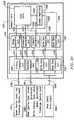
- FIG. 1shows the general organization of a memory device.
- Memory device 101consists of a core 102 and an interface 103 .
- the coreis responsible for storage of the information.
- the interfaceis responsible for translating the external signaling used by the interconnect 105 to the internal signaling carried on bus 104 .
- the primitive operations of the coreinclude at least a read operation.
- there are other operations required to manage the state of the core 102.
- a conventional dynamic random access memory (DRAM)has at least write, precharge, and sense operations in addition to the read operation.
- DRAMdynamic random access memory
- FIG. 2is a block diagram of a conventional DRAM core 102 . Since the structure and operation of a conventional DRAM core is well known in the art only a brief overview is presented here.
- a conventional DRAM core 202mainly comprises storage banks 211 and 221 , row decoder and control circuitry 210 , and column data path circuit comprising column amplifiers 260 and column decoder and control circuitry 230 .
- Each of the storage bankscomprises storage arrays 213 and 223 and sense amplifiers 212 and 222 .
- the row and column decodersmay be replicated in order to form the logical decoder shown in FIG. 2 .
- the column i/o lines 245may be either bidirectional, as shown, or unidirectional, in which case separate column i/o lines are provided for read and write operations.
- Row operationscontrol the storage array word lines 241 and the sense amplifiers via line 242 . These operations control the movement of data from the selected row of the selected storage array to the selected sense amplifier via the bit lines 251 and 252 .
- Column operationscontrol the movement of data from the selected sense amplifiers to and from the external data connections 204 d and 204 e.
- Device selectionis generally accomplished by one of the following choices:
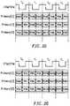
- FIG. 3illustrates the timing required to perform the row operations of precharge and sense. In their abstract form these operations can be defined as
- PRECH and PRECHBANKform signals on line 204 a in which PRECHBANK presents the “bank” argument of the precharge operation
- SENSE, SENSEBANK and SENSEROWform signals on line 204 b in which SENSEBANK and SENSEROW present the “bank” and “row” arguments, respectively, for the sense operation.
- t RP , t RAS,min and t RCDcan have significant variations between devices using the same design and across different designs using the same architecture.
- FIG. 5 and FIG. 6illustrate the timing requirements of the read and write operations, respectively. These operations can be defined abstractly as:
- More recent conventional DRAM coresallow a certain amount of concurrent operation between the functional blocks of the core. For example, it is possible to independently operate the precharge and sense operations or to operate the column path simultaneously with row operations. To take advantage of this concurrency each of the following groups may operate somewhat independently:
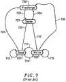
- FIG. 7shows the permissible sequence of operations for a single bank of a conventional DRAM core. It shows the precharge 720 , sense 721 , read 722 , and write 723 , operations as nodes in a graph. Each directed arc between operations indicates an operation which may follow. For example, arc 701 indicates that a precharge operation may follow a read operation.
- This universal sequenceallows any sequence of operations needed by an application to be performed in one pass through it without repeating any step in that sequence.
- a control mechanism that implements the universal sequencecan be said to be conflict free.
- a conflict free control mechanismpermits a new application reference to be started for every minimum data transfer. That is, the control mechanism itself will never introduce a resource restriction that stalls the memory requestor. There may be other reasons to stall the memory requestor, for example references to different rows of the same bank may introduce bank contention, but lack of control resources will not be a reason for stalling the memory requester
- Memory applicationsmay be categorized as follows:
- unified applicationscombine the characteristics of main memory and graphics memory traffic. As electronic systems achieve higher and higher levels of integration the ability to handle these combined reference streams becomes more and more important.
- the control bandwidthis generally dominated by the addressing information delivered to the memory device.
- the service timeis the amount of time required to satisfy a request once it is presented to the memory system. Latency is the service time of a request when the memory system is otherwise devoid of traffic. Resource conflicts, either for the interconnect between the requester and the memory devices, or for resources internal to the memory devices such as the banks, generally determine the difference between latency and service time. It is desirable to minimize average service time, especially for processor traffic.
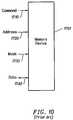
- FIG. 9shows the die of a memory device 1601 inside of a package 1620 .
- the bond padssuch as 1610
- the bond padshave center to center spacing significantly less than the pins of the device, such as 1640 . This requires that there be some fan-in from the external pins to the internal bonding pads.
- the length of the package wiringsuch as 1630 , grows. Observe that elements 1630 and 1640 are alternately used to designate package wiring.
- the overall size of the packageincreases, which costs more to produce and requires more area and volume when the package is installed in the next level of the packaging hierarchy, such as on a printed circuit board.
- the stub created by the longer package wiringcan affect the speed of the interconnect.
- mismatch in package wiring lengths due to the fan-in anglecan affect the speed of the interconnect due to mismatched parasitics.
- the total number of signal pinshas effects throughout the packaging hierarchy. For example, the memory device package requires more material, the next level of interconnect, such as a printed circuit board, requires more area, if connectors are used they will be more expensive, and the package and die area of the master device will grow.
- each signal pinespecially high speed signal pins, requires additional power to run the transmitters and receivers in both the memory devices as well as the master device. Added power translates to added cost since the power is supplied and then dissipated with heat sinks.
- the memory device illustrated in FIG. 10uses techniques typical of present day memory devices.
- a single shared command bus 1710 in conjunction with the single address bus 1720 and mask bus 1730is used to specify all of the primitive operations comprising precharge, sense, read, and write in addition to any other overhead operations such as power management.
- FIG. 11illustrates the operation of the memory device of FIG. 10 .
- the illustrated reference sequencewhen classified according to Table 2 and the universal sequence previously described comprises:
- each boxrepresents the amount of time required to transfer one bit of information across a pin of the device.
- FIG. 11can be used to illustrate a number of techniques for specifying data transfers.
- One prior art techniqueuses an internal register to specify the number of data packets transferred for each read or write operation. When this register is set to its minimum value and the reference is anything besides a hit then the device has insufficient control bandwidth to specify all the required operations while simultaneously keeping the data pins highly utilized. This is shown in FIG. 11 by the gaps between data transfers. For example there is a gap between data a, 1881 and data b, 1882 . Even if sufficient control bandwidth were provided some prior art devices would also require modifications to their memory cores in order to support high data pin utilization.
- Read operationsdo not require masking information. This leaves the mask pins 1830 available for other functions. Alternately, the mask pins during read operations may specify which bytes should actually be driven across the pins as illustrated by box 1873 .
- Another techniqueis an alternative method of specifying that a precharge should occur by linking it to a read or write operation. When this is done the address components of the precharge operation need not be respecified; instead, a single bit can be used to specify that the precharge should occur.
- One prior art method of coding this bitis to share an address bit not otherwise needed during a read or write operation. This is illustrated by the “A-Prech” boxes, 1861 and 1862 .
- FIG. 12shows a sequence of four read references each comprising all the steps of the universal sequence.
- Table 2do not require the multiple precharge steps of the universal sequence it is useful to examine how well a device handles the universal sequence in order to understand its ability to support mixed empty and miss nominal transactions, as well as the transitional transactions of Table 3.
- the data pinsare poorly utilized. This indicates that control contention will limit the ability of the device to transfer data for various mixes of application references. The utilization of the data pins could be improved by making the burst length longer.
- the applicationssuch as graphics applications, require small length transfers rather than large ones.
- Another techniquemakes the delay from write control information to data transfer different from the delay of read control information to data transfer. When writes and reads are mixed, this leads to difficulties in fully utilizing the data pins.
- current memory deviceshave inadequate control bandwidth for many application reference sequences.
- Current memory devicesare unable to handle minimum size transfers.
- current memory devicesutilize the available control bandwidth in ways that do not support efficient applications.
- Current memory devicesdo not schedule the use of the data pins in an efficient manner.
- current memory devicesinefficiently assign a bonding pad for every pin of the device.
- FIG. 1illustrates a known memory structure architecture
- FIG. 2illustrates a known DRAM core structure.
- FIG. 3illustrates Row Access Timing to a single bank in accordance with the prior art.
- FIG. 4illustrates Row Access Timing to different banks in accordance with the prior art.
- FIG. 5illustrates Column Read Timing in accordance with the prior art.
- FIG. 6illustrates Column Write Timing in accordance with the prior art.
- FIG. 7illustrates operation sequences for a conventional core DRAM.
- FIG. 8illustrates initial and final bank states associated with a memory operation in accordance with the prior art.
- FIG. 9illustrates a semiconductor packaging structure utilized in accordance with the prior art.
- FIG. 10illustrates DRAM interface signals in accordance with the prior art.
- FIG. 11illustrates a command control sequence in accordance with the prior art.
- FIG. 12illustrates a unified control universal read sequence in accordance with an embodiment of the invention.
- FIG. 13illustrates a unified control universal read sequence with mask precharge in accordance with an embodiment of the invention.
- FIG. 14illustrates a unified control universal write sequence with mask precharge in accordance with an embodiment of the invention.
- FIG. 15illustrates a unified control universal read write sequence with mask precharge in accordance with an embodiment of the invention.
- FIG. 16illustrates a column access block diagram with no delayed write in accordance with an embodiment of the invention.
- FIG. 17illustrates timing operations associated with a write command of an embodiment of the invention.
- FIG. 18illustrates timing operations associated with a read command of an embodiment of the invention.
- FIG. 19illustrates mixed read and write timing in accordance with an embodiment of the invention.
- FIG. 20illustrates a column access with a delayed write in accordance with an embodiment of the invention.
- FIG. 21illustrates mixed read and write timing in accordance with an embodiment of the invention.
- FIG. 22illustrates a unified control universal read and write sequence with mask precharge and delayed write in accordance with the invention.
- FIG. 23illustrates a split control universal read write sequence with mask precharge and delayed write in accordance with an embodiment of the invention.
- FIG. 24illustrates a cost optimized highly concurrent memory in accordance with the invention.
- FIG. 25illustrates a control packet format for encoding the sense operation on the primary control lines in accordance with an embodiment of the invention.
- FIG. 26illustrates a control packet format for encoding the precharge operation on the primary control lines in accordance with an embodiment of the invention.
- FIG. 27illustrates a packet format when masking is not used on the secondary control lines of the invention.
- FIG. 28illustrates a packet format when masking is used on the secondary control lines of the invention.
- FIG. 29illustrates a data block timing diagram for data packets transmitted on data wires of the invention.
- FIG. 30illustrates a read hit in accordance with an embodiment of the invention.
- FIG. 31illustrates an empty read in accordance with an embodiment of the invention.
- FIG. 32illustrates a read miss in accordance with an embodiment of the invention.
- FIG. 33illustrates a write hit in accordance with an embodiment of the invention.
- FIG. 34illustrates an empty write in accordance with an embodiment of the invention.
- FIG. 35illustrates a write miss in accordance with an embodiment of the invention.
- FIG. 36illustrates reads in accordance with an embodiment of the invention.
- FIG. 37illustrates empty byte masked writes in accordance with an embodiment of the invention.
- FIG. 38illustrates byte masked write hits in accordance with an embodiment of the invention.
- FIG. 39illustrates byte masked write misses in accordance with an embodiment of the invention.
- FIG. 40illustrates reads or unmasked writes in accordance with an embodiment of the invention.
- FIG. 41illustrates universal byte masked writes in accordance with an embodiment of the invention.
- FIG. 42illustrates reads or unmasked writes in accordance with an embodiment of the invention.
- FIG. 43illustrates reads or masked writes or unmasked writes in accordance with an embodiment of the invention.
- FIG. 44illustrates reads and unmasked writes in accordance with an embodiment of the invention.
- FIG. 45illustrates transfers using a primary control packet for sense and precharge in accordance with an embodiment of the invention.
- FIG. 46illustrates a memory block constructed in accordance with an embodiment of the invention.
- FIG. 47illustrates DRAM refresh operations utilized in connection with an embodiment of the invention.
- FIG. 48illustrates isolation pins without accompanying pads in accordance with an embodiment of the invention.
- FIG. 49illustrates the transport of auxiliary information in accordance with an embodiment of the invention.
- FIG. 50illustrates framing of the CMD for processing by the auxiliary transport unit in accordance with an embodiment of the invention.
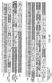
- FIG. 13shows a timing diagram according to an embodiment of the present invention in which the Mask pins 2030 carry a precharge specification rather than either the write mask information or the tristate control information, as shown in connection with FIG. 12 .
- This use of the Mask pinsneed not be exclusive. There are multiple ways in which to indicate how the information presented on the Mask pins is to be used. For example:
- one pinindicates whether an operation should occur and the other pin indicates which bank to precharge.
- more banksare addressed by using the same pins for more than one cycle to extend the size of the bank address field.
- the deviceis specified in some other operation.
- the precharge specified by the mask pinsshares device selection with a chip select pin that also conditions the main command pins.
- additional control bandwidthis added to the device.
- an additional chip select pinis added for sole use by the recoded mask pin precharge.
- the device addressis coded on the additional bits, the device address being compared to an internal device address register.
- FIG. 13it can be seen that the data pins are better utilized.
- the offset between data block 1982 and 1983 in FIG. 12is reduced from 4 units of time to the 2 units of time between data blocks 2082 and 2083 of FIG. 13 .
- FIG. 14shows the timing of the universal write sequence in an embodiment according to the present invention, when the Mask pins are used for the precharge step.
- the offset from data block 2182 to data block 2183is two units of time just as in the read sequence shown in FIG. 13 .
- the offset from the use of the command pins to the use of the data pinsis shown as zero for the write case but three for the read case.
- FIG. 15when these sequences are combined to produce a sequence that has both reads and writes, there is a substantial gap between the write data and the read data as can be seen by the delay between data 2282 and data 2283 . Delaying the write data so that the offset from control information to data is the same, independent of whether the transfer is a read or a write, reduces or eliminates the delay.
- FIG. 16shows the column access path of a memory device in an embodiment of the invention that does not delay write data with respect to read data.
- the delay from external control 2304 to internal column control 2306is identical whether the access is a read or a write.
- a readuses resources in the order: (a) control interconnect 2304 , (b) column i/o 2307 , (c) data interconnect 2305 .
- a writeuses them in the order: (a) control interconnect 2304 , (b) data interconnect 2305 , (c) column i/o 2307 .
- the resource ordering of writesgenerally leads to the resource timing shown in FIG. 17 .
- a writeuses resource as shown by block 2440 , the data resource as shown by block 2450 , and the column resource as shown by the block 2460 . This resource timing minimizes the control logic and the latency of writing data into the memory core.
- the read resource timing of FIG. 18illustrates a minimum latency read via block 2540 , column i/o block 2560 , and data block 2550 .
- a data bubbleis introduced between blocks 2652 and 2653 of FIG. 19 .
- This data bubbleconstitutes time during which the data pins are not being utilized to transfer data; the pins are inactive. Forcing the data pins to do nothing as a result of mixing reads and writes is a problem.
- the data bubbleappears regardless of whether the write 2642 and the read 2643 are directed to the same or different memory devices on the channel. Further note that the delay from the control resource to the column i/o resource is identical for reads and writes. In view of this, it is impossible for the data resource timing to be identical for reads and writes.
- the optimal delay for a writedoes not quite match the delay for a read. Instead, it should be the minimum read delay minus the minimum turnaround time. Since the turnaround delay grows as the read delay grows, there is no need to change the write control to data delay as a function of the memory device position on the channel.
- FIG. 20shows an embodiment of the invention having delayed write circuitry.
- the column access control information on line 2706is delayed for writes relative to when the column control information is presented to the core for reads.
- FIG. 20shows multiplexor 2712 which selects between the write delay block 2709 and the normal column control output of the interface.
- the interfacecontrols the multiplexor depending upon whether the transfer is a read or a write.
- a state machinecould introduce new delaying state transitions when the transfer is a write.
- FIG. 21shows the operation of delaying the write to match the read in accordance with the present invention.
- the delay from write control block 2842 to write data block 2852is set to match the delay from read control 2843 block to read data 2853 block less the channel turnaround time.
- the data bubbleis reduced to the minimum required by channel turnaround requirements and is no longer a function of control or data resource conflicts.
- Delayed writeshelp optimize data bandwidth efficiency over a set of bidirectional data pins.
- One methodadds delay between the control and write data packets so that the delay between them is the same or similar as that for read operations. Keeping this Apattern ⁇ the same or similar for reads and writes improves pipeline efficiency over a set of bidirectional data pins, but at the expense of added complexity in the interface.
- FIG. 22shows that the offset between write data 2984 block and read data 2985 block has been reduced by 2 units of time, compared to the analogous situation of FIG. 15 .
- FIG. 22shows less than full utilization of the data interconnect due to the overloaded use of the command pins 2910 .
- the command pinscan be partitioned so that these operations are delivered to the device in an independent fashion.
- the timing of such a control methodis shown in FIG. 23 where the unified control has been partitioned into fields of control information, labeled primary field 3011 and secondary field 3012 .
- the primary control pinscan be used to control the sense operation while the secondary control pins control read or write operations.
- An embodiment of the present inventionallows full utilization of the data pins and can transfer minimum size data blocks back-to-back, for any mix of reads or unmasked writes, for any mix of hits, misses, or empty traffic, to or from any device, any bank, any row, and any column address with only bank conflict, channel turnaround at the write-read boundaries, and 2nd order effects such as refresh limiting the data channel utilization.
- the writescould be masked or unmasked.
- FIG. 23presumes that the memory device is designed for an interconnect structure that has zero turnaround delay between writes and reads.
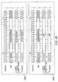
- FIG. 24shows an embodiment of the invention that has separate control interconnect resources. In one embodiment it uses delayed writes. In another embodiment it can alternately specify either a masking or a precharge field, either singly or in conjunction with another field. In another embodiment it combines delayed writes and the masking versus precharge. In an alternative embodiment according to the present invention there are three methods for starting a precharge operation in the memory core:
- Table 4shows the specific logical pinout of the embodiment of FIG. 24 to be used for this illustrative purpose.
- FIG. 24Name Count Description Reference Primary[2:0] 3 Primary request control 3104 Secondary[4:0] 5 Secondary request control 3105 DQA[8:0] 9 Low order data byte 3106 DQB[8:0] 9 High order data byte
- FIG. 25 and FIG. 26show two alternative control packet formats for encoding, respectively, the sense and precharge operations on the primary control lines.
- Table 5defines the fields in the alternative formats of the primary control packet.
- the PD fieldselects a specific memory device.
- a combined fieldcarries both the bank and row address arguments of the sense operation, as previously defined.
- FIG. 27 and FIG. 28show two alternative control packet formats for encoding various operations on the secondary control lines.
- FIG. 27shows the packet format when masking is not being performed while FIG. 28 shows the format when masking is being performed.
- Table 6defines the fields in either format of the secondary control packet. Packet framing is accomplished via a framing bit.
- the M fieldis used to indicate which format of the packet is being presented as well as indicating whether write data being written to the core should be masked.
- the SO fieldindicates whether a read or write operation should be performed.
- Device selection for SO specified operationsis accomplished according to the SD field which is compared against an internal register that specifies the device address.
- the SA fieldencodes the column address of a read or write operation.
- the SB fieldencodes the bank address of a read or write operation.
- the precharge operationuses the SD device and SB bank address.
- the SRC fieldis used for power management functions.
- the MA and MB fieldsprovide a byte masking capability when the M field indicates masking.
- the XO, XD, and XB fieldsprovide the capability to specify a precharge operation when the M field does not indicate masking. Note that, unlike the SPC field, this specification of a precharge has a fully independent device, XD, and bank address, XB, that is not related to the read or write operations.
- FIG. 29shows the format of the data packet transmitted on the data wires.
- FIG. 30shows a timing diagram for a nominal read hit.
- a nominal hit referencemeans that the beginning and final state of the addressed bank is open and that the appropriate row is already in the sense amplifiers of the addressed bank. In this case no row operation is required.
- the secondary control packetspecifies the read operation, device address, bank address, and column address. Some time later, the read data is driven on the data pins. In an embodiment according to the present invention it as a constant time, later fixed by the design of the memory device.
- FIG. 31shows a timing diagram for a nominal read empty. Recall that a nominal empty reference means that the beginning and final state of the addressed bank is closed. In order to transfer data, the addressed bank is first sensed, and then, after t RCD , the read operation takes place just as for the read hit of FIG. 30 . Note that this particular example shows the precharge occurring using the primary control packet precharge mechanism. Alternately, other precharge mechanisms are used, since there are no other references contending for the control resources.
- FIG. 32shows a timing diagram for a nominal read miss.
- a nominal miss referencemeans that the beginning and final state of the addressed bank is open, but that the row currently sensed in the bank is not the one addressed by the application reference.
- a precharge operationoccurs, followed by a sense operation, and finally a read operation that causes the proper data to be driven out on the data pins. Any precharge mechanisms can be used.
- FIG. 33shows a nominal write hit.
- the figurerelates to a multistep write operation.
- This second secondary control packetprovides a timing reference that indicates to the memory device that it is time to send the data to the core.
- FIG. 34shows a timing diagram for a nominal write empty.
- a write empty operationis a combination of the actions needed for a read empty and a write hit. First, a sense operation is performed, followed by a write operation, including the secondary control packet, followed by some precharge operation, although a primary precharge operation is shown.
- FIG. 35illustrates a timing diagram for a nominal write miss.
- Write miss operationis a combination of the actions needed for a read miss and a write hit.
- a precharge operationis invoked; a primary precharge operation is shown.
- a sense operationfollows, along with the two secondary control packets needed to write the data all the way to the memory core.
- FIG. 36illustrates how one of these isolated references can be used for a sequence of memory references.
- a sequence of nominal read empty referencesis shown.
- the XO precharge operationis used to perform the close operation at the end of the sequence.
- the present inventionthus provides another precharge mechanism that neither overloads the external control pin resources, nor adds logic to the memory device.
- FIG. 37shows timing for a series of nominal masked write empty references.
- the XO precharge operationis not available because those control pin resources are being used to supply the mask information.
- the SPC fieldis used in order to avoid bubbles, since the primary control pins are already committed to the series of sense operations. Presuming that the delay between sense and write operations is such that write read conflict problems are being avoided, as shown with the previous discussion on delayed writes, there is no real penalty for using the SPC field. This is different from reads, which would normally complete, and which desire to complete, sooner. This asymmetry between reads and writes leads to the cost reductions of the present invention by reducing required control bandwidth, while minimally impacting application performance.
- FIG. 38shows a series of nominal masked write hit references. Note that although two secondary control packets were required to fully write data into the memory core for an isolated reference the average number needed is about one.
- FIG. 39shows a timing diagram for a series of masked writes misses.
- the SPC fieldis used to precharge the bank.
- Such a sequenceis useful in a graphics application which varies the length of time it keeps any bank open depending upon the amount of rendering to be done. If more than one transfer is directed to the same row of the same bank of the same device then some of the SPC precharge operations and the corresponding sense operations can be removed. This is useful both to eliminate unnecessary (precharge, sense) power but also to reduce the effective number of independent banks required to sustain the effective bandwidth, even when bank conflicts might occur.
- FIG. 40shows a timing diagram for the universal sequence for minimum size transfers when the write traffic is not masked.
- the XO precharge operationcan be consistently used for the precharge operation which begins the universal sequence, while the SPC field is used for the close operation which ends the universal sequence.
- the processor cache miss traffictypically does not contain frequent masked write activity but is latency sensitive. Since it does not use the masking capability it can use the XO precharge capability.
- FIG. 41demonstrates the extra degree of freedom permitted when the transfer size per (sense, precharge) pair is twice the minimum transfer size. In this case some of the primary control bandwidth becomes available for precharge control. In this case the universal sequence can be implemented even for masked writes.
- FIG. 42shows a timing diagram for the universal sequence for reads and unmasked writes when the transfer size is twice the minimum per (precharge, sense) pair.
- the precharge step of the universal sequenceis scheduled with the primary packet precharge while the close step is scheduled with the XO precharge.
- the close stepis scheduled with the XO precharge.
- not onlyis there adequate control bandwidth but there is more scheduling freedom for each of the steps of the universal sequence compared to the minimum transfer size per (precharge, sense) pair case.
- FIG. 43shows a timing diagram for universal reads or masked writes or unmasked writes.
- the precharge step of the universal sequenceis still scheduled in the primary control packet but the close step is scheduled with the XO precharge operation. This reduces the scheduling flexibility compared to the unmasked case 24 but still permits full data pin utilization.
- FIG. 45shows a timing diagram for another scheduling alternative when the transfer size is twice the minimum per (precharge, sense) pair and the traffic consists of all empty references. In this case both the sense and precharge can be scheduled on the primary control pins.
- FIG. 46shows an alternative embodiment that includes all of the features of FIG. 24 , but includes additional capability to initialize, read and write registers, and supply power control information to the memory device.
- the pinout of this embodimentis summarized in Table 8.
- FIG. 46Reference CTM 2 RSL Transmit Clock 5301 CTMN (Clock To Master) CFM 2 RSL Receive Clock CFMN (Clock From Master) Primary[2:0] 3 RSL Primary request control 5305 Secondary[4:0] 5 RSL Secondary request control 5305 DQA[8:0] 9 RSL Low order data byte 5307 DQB[8:0] 9 RSL High order data byte SIO[1:0] 2 CMOS Bidirectional serial in/out for 5302 and 5304 device initialization, register ops, power mode control, and device reset. Used to form the SIO daisy chain. SCK 1 CMOS Serial clock for SIO and CMD 5303 pins. CMD 1 CMOS Command input used for 5302 power mode control, configuring SIO daisy chain, and framing SIO operations.
- FIG. 47shows the operation sequence for the alternative embodiment of FIG. 46 .
- the refresh specific operationssupport a novel method of handling core refresh. These new core operations create the requirements for the Refresh and RefreshS operations coded in the primary control packet as shown in FIG. 46 .
- various power control operationsare added to the primary control packet.
- FIG. 48shows an embodiment of the physical construction in which not all of the pins of the memory device are connected to the bond pads of the die.
- These non-connected pinsprovide signal isolation and shielding, thus avoiding the expense of additional bond pads.
- pin and internal conductor 5542provides isolation for pin and internal conductors 5541 and 5543 .
- the non-connected pinsare signal returns, such as ground, which are adjacent to the connected pins.
- the memory device of FIG. 46has Auxiliary information 5302 transported in time according to FIG. 49 .
- Auxiliary information 5302includes a field to specify an auxiliary operation, a control register address in the memory device, and data to be read or written from or to the control register.
- AuxClockis the AuxClock signal to the Auxiliary Transport Unit 5308 and is used to receive information from the auxiliary connections 5302 in FIG. 46 . Since Auxiliary Transport Unit 5308 operates to reset or initialize the memory device, the unit need only operate slowly. Accordingly, information is framed by the CMD signal, which can be a portion of the auxiliary connections 5302 , and received on the AuxIn signal as a serial bit stream.
- the format of the bit streamis shown in the tables below. As can be noted from Table 9 there are sixteen clock cycles during which a packet of information is received or obtained from the Auxiliary Transport Unit.
- the Aux information fieldsare the SOP[3:0] field and the SDEV[4:0] field for the SRQ packet.
- the SA packethas field SA[11:0]
- the SINT packethas a field of all zeros
- the SD packethas SD[15:0].
- the SRQ, SA, SINT and SD packetsare received or obtained from the Auxiliary Transport unit in the order listed, unless only the SRQ packet is needed, in which case the other packets are not sent.
- the functions of each of the fields in the packetsis tabulated in Table 10.
- the memory deviceis selected by the SDEV field and the SOP field determines the Auxiliary Operation to be performed by the Register Operation Unit 5309 in FIG. 46 .
- the Auxiliary Transport Unitalso supports the initialization of the memory device because the Auxiliary Transport Unit itself does not require initialization. This function is shown in FIG. 49 .
- the CMD signal received by the Auxiliary Transport Unithas different framing information to indicate that an initialization packet follows. This causes all of the memory devices which are connected together on the same external connections in FIG. 46 to break apart a daisy chain connection formed from AuxIn through AuxOut to AuxIn of the next memory device in the chain as the initialization packet passes through the daisy chain.
- the first memory device in the chainreceives a device identification field from the Auxiliary Transport unit into one of its control registers. This field serves to identify the device for future Auxiliary Transport Operations.
- the device field registeris written again to change a bit, causing the first device in the chain to pass the Auxiliary information it receives to the next device in the chain. The sequence is repeated until all of the memory devices have their control registers properly configured and each device has an unique identification.
- the memory device of FIG. 46receives power control information, specifying a change in the power mode of the memory device. While power control operations such as Powerdown and Nap are encoded into the precharge packets in one embodiment according to the present invention, other power control operations, such as ExitToNormal and ExitToDrowsy come in through the Auxiliary Transport Unit because the other units in FIG. 46 are not operational due to their reduced power state and because the Auxiliary Transport Unit operates relatively slowly compared to, for example, the Transfer Units, and so does not require much power while the other units are in their reduced power state. These Exit operations may be performed according to FIG. 50 . FIG.
- the Auxiliary Transport Unitcan recognize the ExitToNormal or ExitToDrowsy request.
- the memory devicewhen a memory device receives a CMD signal 01 with 0 on the falling edge of AuxClock and 1 on the rising edge of AuxClock, the memory device will exit either the power down state or the nap state (Power State A in the timing diagram) and move to a new power state (Power State B in the diagram), depending on the state of the AuxIn Signal Line. If the AuxIn line is a 1, the memory device will exit to the normal state and if the AuxIn line is a 0 the memory device will exit to the drowsy state.
- the meaning of the AuxIn bitsis reversed.
- the device that is targeted for the ExitToNormal or ExitToDrowsy operationis received by the Auxiliary Transport Unit 5308 on the data input field via path 5307 of the memory device in FIG. 46 .
- each memory devicereceives a different CMD signal, one for each device, rather than using the data input field via path 5307 to identify the device for a ExitToNormal or ExitToDrowsy operation.
Landscapes
- Engineering & Computer Science (AREA)
- Microelectronics & Electronic Packaging (AREA)
- Computer Hardware Design (AREA)
- Databases & Information Systems (AREA)
- Dram (AREA)
Abstract
Description
This application is a continuation of U.S. patent application Ser. No. 11/953,803, filed Dec. 10, 2007 now U.S. Pat. No. 7,496,709, which is a continuation of U.S. patent application Ser. No. 11/692,159, filed Mar. 27, 2007, now U.S. Pat. No. 7,330,952, which is a continuation of U.S. patent application Ser. No. 11/059,216, filed Feb. 15, 2005, now U.S. Pat. No. 7,197,611, which is a continuation of U.S. patent application Ser. No. 10/128,167, filed Apr. 22, 2002, now U.S. Pat. No. 6,868,474, which is a divisional of U.S. patent application Ser. No. 09/169,206, filed Oct. 9, 1998, now U.S. Pat. No. 6,401,167, which claims priority to U.S. Provisional Patent Application No. 60/061,770, filed Oct. 10, 1997, all of which are herein incorporated by referenced in their entirety.
The present invention relates generally to electronic systems for data storage and retrieval. More particularly, the invention is directed toward improved methods and structures for memory devices.
In any engineered design there are compromises between cost and performance. The present invention introduces novel methods and structures for reducing the cost of memory devices while minimally compromising their performance. The description of the invention requires a significant amount of background including: application requirements, memory device physical construction, and memory device logical operation.
Memory device application requirements can be most easily understood with respect to memory device operation.FIG. 1 shows the general organization of a memory device.Memory device 101 consists of acore 102 and aninterface 103. The core is responsible for storage of the information. The interface is responsible for translating the external signaling used by theinterconnect 105 to the internal signaling carried onbus 104. The primitive operations of the core include at least a read operation. Generally, there are other operations required to manage the state of thecore 102. For example, a conventional dynamic random access memory (DRAM) has at least write, precharge, and sense operations in addition to the read operation.
For purposes of illustrating the invention a conventional DRAM core will be described.FIG. 2 is a block diagram of aconventional DRAM core 102. Since the structure and operation of a conventional DRAM core is well known in the art only a brief overview is presented here.
Aconventional DRAM core 202 mainly comprisesstorage banks control circuitry 210, and column data path circuit comprisingcolumn amplifiers 260 and column decoder andcontrol circuitry 230. Each of the storage banks comprisesstorage arrays sense amplifiers
There may be many banks, rather than just the two illustrated. Physically the row and column decoders may be replicated in order to form the logical decoder shown inFIG. 2 . The column i/o lines 245 may be either bidirectional, as shown, or unidirectional, in which case separate column i/o lines are provided for read and write operations.
The operation of a conventional DRAM core is divided between row and column operations. Row operations control the storagearray word lines 241 and the sense amplifiers vialine 242. These operations control the movement of data from the selected row of the selected storage array to the selected sense amplifier via thebit lines external data connections
Device selection is generally accomplished by one of the following choices:
- matching an externally presented device address against an internally stored device address;
- requiring separate operation control lines, such as RAS and CAS, for each set of memory devices that are to be operated in parallel; and
- providing at least one chip select control on the memory device.
- precharge(device, bank)—prepare the selected bank of the selected device for sensing; and
- sense(device, bank, row)—sense the selected row of the selected bank of the selected device.
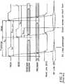
The operations and device selection arguments are presented to the core via the PRECH and SENSE timing signals while the remaining arguments are presented as signals which have setup and hold relationships to the timing signals. Specifically, as shown inFIGS. 2-4 , PRECH and PRECHBANK form signals online 204ain which PRECHBANK presents the “bank” argument of the precharge operation, while SENSE, SENSEBANK and SENSEROW form signals on line204bin which SENSEBANK and SENSEROW present the “bank” and “row” arguments, respectively, for the sense operation. Each of the key primary row timing parameters, tRP, tRAS,minand tRCDcan have significant variations between devices using the same design and across different designs using the same architecture.
- data=read(device, bank, column)—transfer the data in the subset of the sense amplifiers specified by “column” in the selected “bank” of the selected “device” to the READDATA lines; and
- write (device, bank, column, mask, data)—store the data presented on the WRITEDATA lines into the subset of the sense amplifiers specified by “column” in the selected “bank” of the selected “device”; optionally store only a portion of the information as specified by “mask”.
More recent conventional DRAM cores allow a certain amount of concurrent operation between the functional blocks of the core. For example, it is possible to independently operate the precharge and sense operations or to operate the column path simultaneously with row operations. To take advantage of this concurrency each of the following groups may operate somewhat independently:
- PRECH and PRECHBANK on
lines 204a; - SENSE, SENSEBANK, and SENSEROW on lines204b;
- COLCYC204fon line, COLLAT and COLADDR on lines204g, WRITE and WMASK one
lines 204c, READDATA online 204d, and WRITEDATA on line204.
- PRECH and PRECHBANK on
There are some restrictions on this independence. For example, as shown inFIG. 3 , operations on the same bank observe the timing restrictions of tRPand tRAS,min. If accesses are to different banks, then the restrictions ofFIG. 4 for tSSand tPPmay have to be observed.
The present invention, while not limited by such values, has been optimized to typical values as shown in Table 1.
| TABLE 1 |
| Typical Core Timing Values |
| Symbol | Value (ns) | ||
| tRP | 20 | ||
| tRAS,Min | 50 | ||
| tRCD | 20 | ||
| tPP | 20 | ||
| tSS | 20 | ||
| tPC | 10 | ||
| 7 | |||
The series of memory operations needed to satisfy any application request can be covered by the nominal and transitional operation sequences described in Table 2 and Table 3. These sequences are characterized by the initial and final bank states as shown inFIG. 8 .
The sequence of memory operations is relatively limited. In particular, there is a universal sequence:
- precharge,
- sense,
- transfer (read or write), and
- close.
In this sequence, close is an alternative timing of precharge but is otherwise functionally identical. This universal sequence allows any sequence of operations needed by an application to be performed in one pass through it without repeating any step in that sequence. A control mechanism that implements the universal sequence can be said to be conflict free. A conflict free control mechanism permits a new application reference to be started for every minimum data transfer. That is, the control mechanism itself will never introduce a resource restriction that stalls the memory requestor. There may be other reasons to stall the memory requestor, for example references to different rows of the same bank may introduce bank contention, but lack of control resources will not be a reason for stalling the memory requester
| TABLE 2 |
| Nominal Transactions |
| Initial Bank | Transaction | ||
| State | Final Bank State | Type | Operations Performed |
| closed | closed | empty | sense, |
| series of column | |||
| operations, | |||
| precharge | |||
| open | open | miss | precharge, |
| sense, | |||
| series of column | |||
| operations | |||
| hit | series of column | ||
| operations | |||
| TABLE 3 |
| Transitional Transactions |
| Initial Bank | Transaction | ||
| State | Final Bank State | Type | Operations Performed |
| closed | open | empty | sense, |
| <series of column | |||
| operations>(optional) | |||
| open | closed | miss | <precharge, |
| sense, | |||
| series of column | |||
| operations>(optional), | |||
| precharge | |||
| hit | <series of column | ||
| operations> | |||
| (optional), | |||
| precharge | |||
Memory applications may be categorized as follows:
- main memory—references generated by a processor, typically with several levels of caches;
- graphics—references generated by rendering and display refresh engines; and
- unified—combining the reference streams of main memory and graphics.
Applications may also be categorized by their reference stream characteristics. According to the application partition mentioned above reference streams can be characterized in the following fashion:
- First, main memory traffic can be cached or uncached processor references. Such traffic is latency sensitive since typically a processor will stall when it gets a cache miss or for any other reason needs data fetched from main memory. Addressing granularity requirements are set by the transfer size of the processor cache which connects to main memory. A typical value for the cache transfer size is 32 bytes. Since multiple memory interfaces may run in parallel it is desirable that the memory system perform well for transfer sizes smaller than this. Main memory traffic is generally not masked; that is, the vast bulk of its references are cache replacements which need not be written at any finer granularity than the cache transfer size.
- Another type of reference stream is for graphics memory. Graphics memory traffic tends to be bandwidth sensitive rather than latency sensitive. This is true because the two basic graphics engines, rendering and display refresh, can both be highly pipelined. Latency is still important since longer latency requires larger buffers in the controller and causes other second order problems. The ability to address small quanta of information is important since typical graphics data structures are manipulated according to the size of the triangle being rendered, which can be quite small. If small quanta cannot be accessed then bandwidth will be wasted transferring information which is not actually used. Traditional graphics rendering algorithms benefit substantially from the ability to mask write data; that is, to merge data sent to the memory with data already in the memory. Typically this is done at the byte level, although finer level, e.g. bit level, masking can sometimes be advantageous.
As stated above, unified applications combine the characteristics of main memory and graphics memory traffic. As electronic systems achieve higher and higher levels of integration the ability to handle these combined reference streams becomes more and more important.
Although the present invention can be understood in light of the previous application classification, it will be appreciated by those skilled in the art that the invention is not limited to the mentioned applications and combinations but has far wider application. In addition to the specific performance and functionality characteristics mentioned above it is generally important to maximize the effective bandwidth of the memory system and minimize the service time. Maximizing effective bandwidth requires achieving a proper balance between control and data transport bandwidth. The control bandwidth is generally dominated by the addressing information delivered to the memory device. The service time is the amount of time required to satisfy a request once it is presented to the memory system. Latency is the service time of a request when the memory system is otherwise devoid of traffic. Resource conflicts, either for the interconnect between the requester and the memory devices, or for resources internal to the memory devices such as the banks, generally determine the difference between latency and service time. It is desirable to minimize average service time, especially for processor traffic.
The previous section introduced the performance aspects of the cost-performance tradeoff that is the subject of the present invention. In this section the cost aspects are discussed. These aspects generally result from the physical construction of a memory device, including the packaging of the device.
There are many negative aspects to the increase in the length of thepackage wiring 1640, including the facts that: the overall size of the package increases, which costs more to produce and requires more area and volume when the package is installed in the next level of the packaging hierarchy, such as on a printed circuit board. Also, the stub created by the longer package wiring can affect the speed of the interconnect. In addition, mismatch in package wiring lengths due to the fan-in angle can affect the speed of the interconnect due to mismatched parasitics.
The total number of signal pins has effects throughout the packaging hierarchy. For example, the memory device package requires more material, the next level of interconnect, such as a printed circuit board, requires more area, if connectors are used they will be more expensive, and the package and die area of the master device will grow.
In addition to all these cost concerns based on area and volume of the physical construction another cost concern is power. Each signal pin, especially high speed signal pins, requires additional power to run the transmitters and receivers in both the memory devices as well as the master device. Added power translates to added cost since the power is supplied and then dissipated with heat sinks.
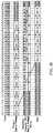
The memory device illustrated inFIG. 10 uses techniques typical of present day memory devices. In thisdevice 1701, a single sharedcommand bus 1710 in conjunction with thesingle address bus 1720 andmask bus 1730 is used to specify all of the primitive operations comprising precharge, sense, read, and write in addition to any other overhead operations such as power management.
- write empty—
sense 1851, write1853 withmask 1871,data 1881, close(precharge)1861; - write miss—precharge1852,
sense 1854, write1856 withmask 1872,data 1882; - read hit—read1857,
tristate control 1873,data 1883; and - transitional write miss—precharge1855,
sense 1858, write1859,mask 1874,data 1884, close(precharge)1862.
- write empty—
InFIG. 11 each box represents the amount of time required to transfer one bit of information across a pin of the device.
In addition to illustrating a specific type of prior art memory device,FIG. 11 can be used to illustrate a number of techniques for specifying data transfers. One prior art technique uses an internal register to specify the number of data packets transferred for each read or write operation. When this register is set to its minimum value and the reference is anything besides a hit then the device has insufficient control bandwidth to specify all the required operations while simultaneously keeping the data pins highly utilized. This is shown inFIG. 11 by the gaps between data transfers. For example there is a gap between data a,1881 and data b,1882. Even if sufficient control bandwidth were provided some prior art devices would also require modifications to their memory cores in order to support high data pin utilization.
The technique of specifying the burst size in a register makes it difficult to mix transfer sizes unless the burst size is always programmed to be the minimum, which then increases control overhead. The increase in control overhead may be so substantial as to render the minimum burst size impractical in many system designs.
Regardless of the transfer burst size, the technique of a single unified control bus, using various combinations of the command pins1810, address pins1820, andmask pins 1830 places limitations on the ability to schedule the primitive operations. A controller which has references in progress that are simultaneously ready to use the control resources must sequentialize them, leading to otherwise unnecessary delay.
Read operations do not require masking information. This leaves the mask pins1830 available for other functions. Alternately, the mask pins during read operations may specify which bytes should actually be driven across the pins as illustrated bybox 1873.
Another technique is an alternative method of specifying that a precharge should occur by linking it to a read or write operation. When this is done the address components of the precharge operation need not be respecified; instead, a single bit can be used to specify that the precharge should occur. One prior art method of coding this bit is to share an address bit not otherwise needed during a read or write operation. This is illustrated by the “A-Prech” boxes,1861 and1862.
Another technique makes the delay from write control information to data transfer different from the delay of read control information to data transfer. When writes and reads are mixed, this leads to difficulties in fully utilizing the data pins.
Thus, current memory devices have inadequate control bandwidth for many application reference sequences. Current memory devices are unable to handle minimum size transfers. Further, current memory devices utilize the available control bandwidth in ways that do not support efficient applications. Current memory devices do not schedule the use of the data pins in an efficient manner. In addition, current memory devices inefficiently assign a bonding pad for every pin of the device.
Like reference numerals refer to corresponding parts throughout the drawings.
- in one embodiment according to the present invention, a register within the device specifies whether the mask pins are to be used for masking, tristate control, or precharge control;
- in another embodiment according to the present invention, the encoding of the command pins is extended to specify, on a per operation basis, how the mask pins are to be used; and
- in another embodiment according to the present invention, a register bit indicates whether tristate control is enabled or not and, in the case it is not enabled, an encoding of the command pins indicates if a write is masked or not; in this embodiment all reads and unmasked writes may use the Mask pins to specify a precharge operation while masked writes do not have this capability since the Mask pins are used for mask information
There are many alternatives for how to code the precharge information on the mask pins. In one embodiment in which there are two mask pins and the memory device has two banks, one pin indicates whether an operation should occur and the other pin indicates which bank to precharge. In an alternative embodiment, in which the minimum data transfer requires more than one cycle, more banks are addressed by using the same pins for more than one cycle to extend the size of the bank address field.
Using the mask pins to specify a precharge operation and the associated bank address requires another way of specifying the device argument. In one embodiment the device is specified in some other operation. For example, the precharge specified by the mask pins shares device selection with a chip select pin that also conditions the main command pins. In another embodiment, additional control bandwidth is added to the device. For example, an additional chip select pin is added for sole use by the recoded mask pin precharge. In yet another example of using additional control bandwidth in which the minimum data transfer requires more than one cycle, the device address is coded on the additional bits, the device address being compared to an internal device address register.
InFIG. 13 it can be seen that the data pins are better utilized. For example, the offset betweendata block FIG. 12 is reduced from 4 units of time to the 2 units of time betweendata blocks FIG. 13 . This is accomplished because the precharge specification has been moved from the primary command pins,2010, to the mask pins2030 so there is more time available on the command pins to specify the sense and read or write operations.
This change in resource ordering gives rise to resource conflict problems that produce data bubbles when mixing reads and writes. The resource ordering of writes generally leads to the resource timing shown inFIG. 17 . For example, a write uses resource as shown byblock 2440, the data resource as shown byblock 2450, and the column resource as shown by theblock 2460. This resource timing minimizes the control logic and the latency of writing data into the memory core.
The read resource timing ofFIG. 18 , illustrates a minimum latency read viablock 2540, column i/o block 2560, anddata block 2550. When these timings are combined as shown inFIG. 19 , a data bubble is introduced betweenblocks FIG. 19 . This data bubble constitutes time during which the data pins are not being utilized to transfer data; the pins are inactive. Forcing the data pins to do nothing as a result of mixing reads and writes is a problem.
Note that the data bubble appears regardless of whether the write2642 and the read2643 are directed to the same or different memory devices on the channel. Further note that the delay from the control resource to the column i/o resource is identical for reads and writes. In view of this, it is impossible for the data resource timing to be identical for reads and writes.
Matching the timing of the write-use of the data resource to the read-use of the data resource avoids the problem stated above. Since the use of the data pins in a system environment has an intrinsic turnaround time for the external interconnect, the optimal delay for a write does not quite match the delay for a read. Instead, it should be the minimum read delay minus the minimum turnaround time. Since the turnaround delay grows as the read delay grows, there is no need to change the write control to data delay as a function of the memory device position on the channel.
Since write latency is not an important metric for application performance, as long as the write occurs before the expiration of tRAS,MIN(so that it does not extend the time the row occupies the sense amplifiers, which reduces application performance), this configuration does not cause any loss in application performance, as long as the writes and reads are directed to separate column data paths.
Delayed writes help optimize data bandwidth efficiency over a set of bidirectional data pins. One method adds delay between the control and write data packets so that the delay between them is the same or similar as that for read operations. Keeping this Apattern≅the same or similar for reads and writes improves pipeline efficiency over a set of bidirectional data pins, but at the expense of added complexity in the interface.
- in the sense operation field on the
primary control lines 3104, as an alternative to the sense information; - in the mask field on the secondary control lines,3105 as an alternative to the mask information; and
- according to the device and bank addresses specified in a read or a write.
- in the sense operation field on the
The benefit of the present invention according to a specific embodiment is shown in Table 4 andFIG. 25 andFIG. 26 . Table 4 shows the specific logical pinout of the embodiment ofFIG. 24 to be used for this illustrative purpose.
| TABLE 4 |
| High Performance Logical Pin Description |
| FIG. 24 | |||
| Name | Count | Description | Reference |
| Primary[2:0] | 3 | 3104 | |
| Secondary[4:0] | 5 | 3105 | |
| DQA[8:0] | 9 | Low | 3106 |
| DQB[8:0] | 9 | High order data byte | |
| TABLE 5 |
| Primary Control Packet Fields |
| Field | Description | ||
| PD4T | |||
| for framing, device selection and broadcasting. | |||
| PD4F | |||
| for framing, device selection and broadcasting. | |||
| PD[3:0] | Device selector, least significant bits. | ||
| AV | Activate row; also indicates format of packet. | ||
| PA[16:0] | Address; combining bank and row. | ||
| PB[5:0] | Bank address | ||
| POP[10:0] | Opcode of the primary control packet. | ||
| TABLE 6 |
| Secondary Control Packet Fields |
| Field | Description | ||
| SD[4:0] | Device selector for Column Operation | ||
| SS = 1 | Start bit; for framing | ||
| M | Mask bit, indicates if mask format is being used | ||
| SO[1:0] | Secondary Operation code | ||
| SPC | Precharge after possible Column Operation | ||
| SRC | Power management | ||
| SA[6:0] | Address for Column Operation | ||
| SB[5:0] | Bank for Column Operation | ||
| MA[7:0] | Byte mask for lower order bytes | ||
| MB[7:0] | Byte mask for higher order bytes | ||
| XD[4:0] | Device selector for Extra Operation | ||
| XO[4:0] | Extra Operation code | ||
| XB[5:0] | Bank for Extra Operation | ||
The operation of this embodiment can be most easily understood through various timing diagrams as shown inFIG. 30 throughFIG. 45 . These figures can be divided into several series, each of which depicts different aspects of this embodiment's operation:
FIG. 30 throughFIG. 35 show a basic operation as an embodiment of the present invention, other operations can be thought of as compositions of these basic operations;FIG. 36 throughFIG. 39 show compositions of the basic operations but distinct from notions of the universal sequence;FIG. 40 throughFIG. 43 show operations according to the universal sequence, these figures demonstrate the ability of the embodiment to handle mixed read and write with mixed hit, miss, and empty traffic without control resource conflicts; andFIG. 44 throughFIG. 45 show operations according to the universal sequence demonstrating less control conflicts than the prior art. Other control scheduling algorithms are possible which seek to minimize other metrics, such as service time, with or without compromising effective bandwidth.
The nominal timings for the examples are shown in Table 7.
| TABLE 7 |
| Nominal Timings |
| Symbol | Value (ns) | ||
| tRP | 20 | ||
| tRAS,min | 60 | ||
| tRCD | 20 | ||
| 20 | |||
A description of each of the timing diagrams follows.
The previous figures show how various application references can be decomposed into the memory operations.FIG. 36 illustrates how one of these isolated references can be used for a sequence of memory references. InFIG. 36 a sequence of nominal read empty references is shown. In this case the XO precharge operation is used to perform the close operation at the end of the sequence. The present invention thus provides another precharge mechanism that neither overloads the external control pin resources, nor adds logic to the memory device.
The previous figures demonstrate the conditions in which the universal sequence can be scheduled. The ability to schedule the universal sequence guarantees that there will not be any control conflicts which reduce available data transfer bandwidth. However, none of the nominal reference sequences actually requires two precharges to be scheduled. So there is generally adequate control bandwidth for various mixes of miss and empty traffic as shown inFIG. 44 .
| TABLE 8 |
| Alternative High Performance Logical Pin Description |
| Name | Count | Type | Description | FIG. 46 |
| CTM | ||||
| 2 | RSL | Transmit | 5301 | |
| CTMN | (Clock To Master) | |||
| 2 | RSL | Receive Clock | ||
| CFMN | (Clock From Master) | |||
| Primary[2:0] | 3 | RSL | 5305 | |
| Secondary[4:0] | 5 | RSL | 5305 | |
| DQA[8:0] | 9 | RSL | Low | 5307 |
| DQB[8:0] | 9 | RSL | High order data byte | |
| SIO[1:0] | 2 | CMOS | Bidirectional serial in/out for | 5302 and 5304 |
| device initialization, register | ||||
| ops, power mode control, and | ||||
| device reset. Used to form the | ||||
| SIO daisy chain. | ||||
| 1 | CMOS | Serial clock for SIO and | 5303 | |
| pins. | ||||
| 1 | CMOS | Command input used for | 5302 | |
| power mode control, | ||||
| configuring SIO daisy chain, | ||||
| and framing SIO operations. | ||||
According to an embodiment of the present invention the memory device ofFIG. 46 hasAuxiliary information 5302 transported in time according toFIG. 49 .Auxiliary information 5302 includes a field to specify an auxiliary operation, a control register address in the memory device, and data to be read or written from or to the control register. AuxClock is the AuxClock signal to theAuxiliary Transport Unit 5308 and is used to receive information from theauxiliary connections 5302 inFIG. 46 . SinceAuxiliary Transport Unit 5308 operates to reset or initialize the memory device, the unit need only operate slowly. Accordingly, information is framed by the CMD signal, which can be a portion of theauxiliary connections 5302, and received on the AuxIn signal as a serial bit stream. The format of the bit stream is shown in the tables below. As can be noted from Table 9 there are sixteen clock cycles during which a packet of information is received or obtained from the Auxiliary Transport Unit. The Aux information fields are the SOP[3:0] field and the SDEV[4:0] field for the SRQ packet. The SA packet has field SA[11:0], the SINT packet has a field of all zeros and the SD packet has SD[15:0]. In this embodiment of the present invention, the SRQ, SA, SINT and SD packets are received or obtained from the Auxiliary Transport unit in the order listed, unless only the SRQ packet is needed, in which case the other packets are not sent. The functions of each of the fields in the packets is tabulated in Table 10.
| TABLE 9 |
| Control Register Packet Formats |
| AuxClock | SRQ packet | SA | SINT | SD | |
| 0 | rsrv | rsrv | 0 | ||
| 1 | rsrv | rsrv | 0 | ||
| 2 | rsrv | rsrv | 0 | ||
| 3 | rsrv | rsrv | 0 | ||
| 4 | SA11 | 0 | |||
| 5 | SA10 | 0 | |||
| 6 | SA9 | 0 | |||
| 7 | SA8 | 0 | |||
| 8 | SA7 | 0 | |||
| 9 | SA6 | 0 | |||
| 10 | SA5 | 0 | |||
| 11 | SA4 | 0 | |||
| 12 | SA3 | 0 | |||
| 13 | SA2 | 0 | |||
| 14 | SA1 | 0 | |||
| 15 | SA0 | 0 | SD0 | ||
| TABLE 10 |
| Field Description for Control Register Packets |
| Field | Description |
| rsrv | Reserved |
| SOP3 . . . SOP0 | Serial opcode. Specifies command for control register transaction. |
| 0000 - SRD. Serial read of control register {SA11 . . . SA0} of | |
| memory device {SDEV4 . . . SDEV0}. | |
| 0001 - SWR. Serial write of control register {SA11 . . . SA0} of | |
| memory device {SDEV4 . . . SDEV0}. | |
| 0010 - SETR. Set Reset bit, all control registers assume their reset | |
| values. | |
| 0011 - CLRR. Clear Reset bit, all control registers retain their | |
| reset values. | |
| 0100 - SETF. Set fast (normal) clock mode for the clock circuitry | |
| SDEV4 . . . SDEV0 | Serial device field. |
| SBC | Serial broadcast. When set, memory device ignores |
| {SDEV4 . . . SDEV0} serial device field | |
| SA11 . . . SA0 | Serial address. Selects which control register of the selected |
| memory device is read or written. | |
| SD15 . . . SD0 | Serial data. The 16 bits of data written to or read from the selected |
| control register of the selected memory device. | |
As is shown in Table 10, the memory device is selected by the SDEV field and the SOP field determines the Auxiliary Operation to be performed by theRegister Operation Unit 5309 inFIG. 46 . The Auxiliary Transport Unit also supports the initialization of the memory device because the Auxiliary Transport Unit itself does not require initialization. This function is shown inFIG. 49 . In this diagram the CMD signal received by the Auxiliary Transport Unit has different framing information to indicate that an initialization packet follows. This causes all of the memory devices which are connected together on the same external connections inFIG. 46 to break apart a daisy chain connection formed from AuxIn through AuxOut to AuxIn of the next memory device in the chain as the initialization packet passes through the daisy chain. Next, the first memory device in the chain receives a device identification field from the Auxiliary Transport unit into one of its control registers. This field serves to identify the device for future Auxiliary Transport Operations. After the memory device has its control registers configured properly, the device field register is written again to change a bit, causing the first device in the chain to pass the Auxiliary information it receives to the next device in the chain. The sequence is repeated until all of the memory devices have their control registers properly configured and each device has an unique identification.
According to an embodiment of the present invention the memory device ofFIG. 46 receives power control information, specifying a change in the power mode of the memory device. While power control operations such as Powerdown and Nap are encoded into the precharge packets in one embodiment according to the present invention, other power control operations, such as ExitToNormal and ExitToDrowsy come in through the Auxiliary Transport Unit because the other units inFIG. 46 are not operational due to their reduced power state and because the Auxiliary Transport Unit operates relatively slowly compared to, for example, the Transfer Units, and so does not require much power while the other units are in their reduced power state. These Exit operations may be performed according toFIG. 50 .FIG. 50 shows a different framing by the CMD signal so that the Auxiliary Transport Unit can recognize the ExitToNormal or ExitToDrowsy request. According to the timing diagram, when a memory device receives a CMD signal 01 with 0 on the falling edge of AuxClock and 1 on the rising edge of AuxClock, the memory device will exit either the power down state or the nap state (Power State A in the timing diagram) and move to a new power state (Power State B in the diagram), depending on the state of the AuxIn Signal Line. If the AuxIn line is a 1, the memory device will exit to the normal state and if the AuxIn line is a 0 the memory device will exit to the drowsy state. In other embodiments, the meaning of the AuxIn bits is reversed. The device that is targeted for the ExitToNormal or ExitToDrowsy operation is received by theAuxiliary Transport Unit 5308 on the data input field viapath 5307 of the memory device inFIG. 46 .
In an alternate embodiment, each memory device receives a different CMD signal, one for each device, rather than using the data input field viapath 5307 to identify the device for a ExitToNormal or ExitToDrowsy operation.
The foregoing description, for purposes of explanation, used specific nomenclature to provide a thorough understanding of the invention. However, it will be apparent to one skilled in the art that the specific details are not required in order to practice the invention. In other instances, well known circuits and devices are shown in block diagram form in order to avoid unnecessary distraction from the underlying invention. Thus, the foregoing descriptions of specific embodiments of the present invention are presented for purposes of illustration and description. They are not intended to be exhaustive or to limit the invention to the precise forms disclosed, obviously many modifications and variations are possible in view of the above teachings. The embodiments were chosen and described in order to best explain the principles of the invention and its practical applications, to thereby enable others skilled in the art to best utilize the invention and various embodiments with various modifications as are suited to the particular use contemplated. It is intended that the scope of the invention be defined by the following claims and their equivalents.
Claims (34)
1. A semiconductor memory device comprising:
a memory core;
a first interface to receive write data from a first set of interconnect resources; and
a second interface, separate from the first interface, the second interface to receive from a second set of interconnect resources:
a column address associated with the write data, wherein the column address identifies a column of the memory core in which to store the write data; and
a first code indicating whether the write data is selectively masked by data mask information, and
wherein, if the first code indicates that the write data is selectively masked, the second interface is to receive data mask information specifying whether to selectively write portions of the write data to the memory core.
2. The semiconductor memory device ofclaim 1 , wherein the second interface is to receive, prior to receiving the column address, a first bit which specifies whether precharging is to occur after the write data is written to the memory core.
3. The semiconductor memory device ofclaim 2 , wherein the second interface is to receive, at the same time that it receives the first bit, a second code that specifies a write operation associated with the write data.
4. The semiconductor memory device ofclaim 3 , wherein the second interface is to receive a bank address specifying a bank of the memory core for the write operation.
5. The semiconductor memory device ofclaim 4 , wherein prior to receiving the column address and the write data, the memory device is to activate a row of the memory core in response to a row activation command, wherein the write data is to be written to the row in connection with the write operation, wherein the column address identifies a column in the row and wherein the row is located in the bank specified by the bank address.
6. The semiconductor memory device ofclaim 5 , further comprising:
an input to receive a clock signal; and
a set of pins to receive a row address that identifies the row of the memory core, wherein for at least one pin of the set of pins, two bits of the row address are received during a clock cycle of the clock signal.
7. The semiconductor memory device ofclaim 6 , wherein the set of pins are included in a third interface that is separate from the first interface and second interface.
8. The semiconductor memory device ofclaim 1 , further comprising an input to receive a clock signal, wherein the first interface comprises a set of pins to receive the write data, wherein for every pin of the set of pins, eight bits of the write data are to be received in succession during four clock cycles of the clock signal.
9. The semiconductor memory device ofclaim 1 , further comprising a third interface, separate from the first interface and the second interface, to receive a row activation command to activate a row of the memory core, wherein the write data is to be written to the row.
10. The semiconductor memory device ofclaim 9 , wherein:
the first interface includes eighteen pins to receive the write data from the first set of interconnect resources, which consists of a data bus that has eighteen signal lines;
the second interface includes five pins to attach to the second set of interconnect resources, which consists of five signal lines; and
the third interface includes three pins to attach to a primary interconnect consisting of three signal lines.
11. A method for controlling a memory device having a memory core, the method comprising:
over a first set of interconnect resources, conveying write data associated with a write operation to the memory device; and
over a second set of interconnect resources that are separate from the first set of interconnect resources:
conveying a column address that identifies a column of the memory core associated with the write operation;
conveying a first code that specifies whether data mask information will be issued in connection with the write operation; and
if the first code specifies that the data mask information will be issued, then conveying the data mask information after conveying the first code, wherein the data mask information specifies whether to selectively write portions of the write data to the memory core.
12. The method ofclaim 11 , wherein conveying the data mask information comprises conveying, over a signal line, two bits of the mask information during a clock cycle of a clock signal that is received by the memory device.
13. The method ofclaim 11 , further comprising, over the second set of interconnect resources, conveying a bit which specifies whether precharging occurs after the write data is written to the memory core.
14. The method ofclaim 13 , further comprising, conveying a column command specifying the write operation.
15. The method ofclaim 14 , further comprising, prior to conveying the column command, conveying a row command that specifies activation of a row of the memory core, wherein the write data is to be written to the row in connection with the write operation, wherein the column is contained in the row.
16. The method ofclaim 15 , wherein the row command is conveyed over a third set of interconnect resources in a first packet format, and the column command is conveyed over the second set of interconnect resources using a second packet format, wherein the third set of interconnect resources are separate from the first and second set of interconnect resources.
17. The method ofclaim 16 , wherein the third set of interconnect resources is a primary interconnect consisting of three signal lines, the second set of interconnect resources is a secondary interconnect consisting of five signal lines, and the first set of interconnect resources is a data bus consisting of eighteen signal lines.
18. A method of controlling a memory device having a plurality of banks, the method comprising:
conveying a row command and a first bank address to activate a row in a bank identified by the first bank address;
conveying a column command and a second bank address, the column command specifying a write operation of write data to a bank identified by the second bank address;
conveying a column address that identifies a column associated with the write operation;
conveying a first code which specifies whether data mask information will be issued in connection with the write operation;
if the first code specifies that the data mask information will be conveyed, then conveying the data mask information after conveying the first code, the data mask information specifying whether to selectively write portions of write data to the memory core;
conveying a first bit which specifies whether precharging occurs after the write data is written to the memory core; and
conveying the write data associated with the write operation, wherein the write data is conveyed over signal lines separate from those used to convey the row command, first bank address, column command, second bank address, the first code and the first bit.
19. The method ofclaim 18 , wherein the row command and first bank address are conveyed as a first packet over a first set of interconnect resources, and the column command, the column address, the first bit, and the first code are conveyed as a second packet over a second set of interconnect resources.
20. The method ofclaim 19 , wherein the first set of interconnect resources is a primary interconnect consisting of three signal lines, and the second set of interconnect resources is a secondary interconnect consisting of five signal lines.
21. The method ofclaim 18 , wherein both a bit of the second bank address and a bit of the column address are conveyed over a common signal line during a clock cycle of a clock signal.
22. The method ofclaim 21 , wherein the first code and first bit are conveyed synchronously with respect to a first transition of the clock signal.
23. The method ofclaim 22 , wherein conveying the data mask information comprises conveying, on a signal line, two bits of the data mask information during a clock cycle of the clock signal.
24. The method ofclaim 22 , wherein the column address and the data mask information are conveyed synchronously with respect to transitions of the clock signal which succeed the first transition of the clock signal.
25. The method ofclaim 18 , wherein the first bank address and the second bank address identify the same bank of the plurality of banks, such that the column address identifies a column of the row activated in the bank identified by both the first and second bank address.
26. The method ofclaim 18 , wherein the first bank address identifies a first bank of the plurality of banks and the second bank address identifies a second bank of the plurality of banks, wherein the first bank and second bank are different banks.
27. The method ofclaim 26 , wherein the row command and the first bank address are conveyed over a first set of interconnect resources during a time in which the column command, the column address, the second bank address, the first bit, and the first code are conveyed over a second set of interconnect resources, wherein the first set of interconnect resources is separate from the second set of interconnect resources.
28. A method of operation of a memory controller that controls a memory device, wherein the memory device receives a write command synchronously with respect to a clock signal to store write data associated with a write operation in a memory core of the memory device, the method comprising:
conveying, on a first signal line, a first code that specifies whether data mask information will be issued in connection with the write operation, wherein the first code is conveyed synchronously with respect to a first transition of the clock signal;
conveying, on a second signal line, precharge information that specifies whether precharging occurs after the write data is written to the memory core, wherein the precharge information is conveyed synchronously with respect to the first transition of the clock signal;
conveying column address information associated with the write operation, wherein a portion of the column address information is conveyed on the first and the second signal lines synchronously with respect to transitions of the clock signal that succeed the first transition of the clock signal;
conveying the write data over a set of lines that are separate from the first signal line and the second signal line; and
if the first code specifies that the data mask information will be issued, then conveying the data mask information to specify whether to selectively write portions of the write data to the memory core, wherein at least a portion of the data mask information is conveyed on the first signal line and the second signal line synchronously with respect to transitions of the clock signal that succeed the first transition of the clock signal.
29. The method ofclaim 28 , wherein conveying the data mask information comprises conveying two bits of the data mask information over the first signal line during a clock cycle of the clock signal.
30. The method ofclaim 28 , further comprising conveying a second code that specifies the write command to the memory device.
31. The method ofclaim 28 , further comprising:
conveying the write command; and
prior to conveying the write command, conveying a row command that specifies activation of a row of the memory core, wherein the column is contained in the row, wherein the write data is to be written to the row in connection with the write operation.
32. The method ofclaim 31 , wherein the row command is conveyed over a primary interconnect that is separate from the first signal line and the second signal line, and wherein the write command is conveyed over a secondary interconnect.
33. The method ofclaim 32 , wherein the row command conveyed over the primary interconnect is included in a first packet format and the write command conveyed over the secondary interconnect is included in a second packet format.
34. The method ofclaim 32 , wherein the primary interconnect consists of three signal lines, and the secondary interconnect consists of five signal lines.
Priority Applications (5)
| Application Number | Priority Date | Filing Date | Title |
|---|---|---|---|
| US12/349,485US7793039B2 (en) | 1997-10-10 | 2009-01-06 | Interface for a semiconductor memory device and method for controlling the interface |
| US12/875,483US8019958B2 (en) | 1997-10-10 | 2010-09-03 | Memory write signaling and methods thereof |
| US13/230,741US8205056B2 (en) | 1997-10-10 | 2011-09-12 | Memory controller for controlling write signaling |
| US13/421,701US8560797B2 (en) | 1997-10-10 | 2012-03-15 | Method and apparatus for indicating mask information |
| US13/421,753US20120173811A1 (en) | 1997-10-10 | 2012-03-15 | Method and Apparatus for Delaying Write Operations |
Applications Claiming Priority (7)
| Application Number | Priority Date | Filing Date | Title |
|---|---|---|---|
| US6177097P | 1997-10-10 | 1997-10-10 | |
| US09/169,206US6401167B1 (en) | 1997-10-10 | 1998-10-09 | High performance cost optimized memory |
| US10/128,167US6868474B2 (en) | 1997-10-10 | 2002-04-22 | High performance cost optimized memory |
| US11/059,216US7197611B2 (en) | 1997-10-10 | 2005-02-15 | Integrated circuit memory device having write latency function |
| US11/692,159US7330952B2 (en) | 1997-10-10 | 2007-03-27 | Integrated circuit memory device having delayed write timing based on read response time |
| US11/953,803US7496709B2 (en) | 1997-10-10 | 2007-12-10 | Integrated circuit memory device having delayed write timing based on read response time |
| US12/349,485US7793039B2 (en) | 1997-10-10 | 2009-01-06 | Interface for a semiconductor memory device and method for controlling the interface |
Related Parent Applications (1)
| Application Number | Title | Priority Date | Filing Date |
|---|---|---|---|
| US11/953,803ContinuationUS7496709B2 (en) | 1997-10-10 | 2007-12-10 | Integrated circuit memory device having delayed write timing based on read response time |
Related Child Applications (1)
| Application Number | Title | Priority Date | Filing Date |
|---|---|---|---|
| US12/875,483ContinuationUS8019958B2 (en) | 1997-10-10 | 2010-09-03 | Memory write signaling and methods thereof |
Publications (2)
| Publication Number | Publication Date |
|---|---|
| US20090129178A1 US20090129178A1 (en) | 2009-05-21 |
| US7793039B2true US7793039B2 (en) | 2010-09-07 |
Family
ID=26741461
Family Applications (13)
| Application Number | Title | Priority Date | Filing Date |
|---|---|---|---|
| US09/169,206Expired - Fee RelatedUS6401167B1 (en) | 1997-10-10 | 1998-10-09 | High performance cost optimized memory |
| US10/128,167Expired - Fee RelatedUS6868474B2 (en) | 1997-10-10 | 2002-04-22 | High performance cost optimized memory |
| US11/059,216Expired - Fee RelatedUS7197611B2 (en) | 1997-10-10 | 2005-02-15 | Integrated circuit memory device having write latency function |
| US11/681,375Expired - Fee RelatedUS7360050B2 (en) | 1997-10-10 | 2007-03-02 | Integrated circuit memory device having delayed write capability |
| US11/681,384Expired - Fee RelatedUS7287119B2 (en) | 1997-10-10 | 2007-03-02 | Integrated circuit memory device with delayed write command processing |
| US11/692,159Expired - Fee RelatedUS7330952B2 (en) | 1997-10-10 | 2007-03-27 | Integrated circuit memory device having delayed write timing based on read response time |
| US11/692,162Expired - Fee RelatedUS7330953B2 (en) | 1997-10-10 | 2007-03-27 | Memory system having delayed write timing |
| US11/953,803Expired - Fee RelatedUS7496709B2 (en) | 1997-10-10 | 2007-12-10 | Integrated circuit memory device having delayed write timing based on read response time |
| US12/349,485Expired - Fee RelatedUS7793039B2 (en) | 1997-10-10 | 2009-01-06 | Interface for a semiconductor memory device and method for controlling the interface |
| US12/875,483Expired - Fee RelatedUS8019958B2 (en) | 1997-10-10 | 2010-09-03 | Memory write signaling and methods thereof |
| US13/230,741Expired - Fee RelatedUS8205056B2 (en) | 1997-10-10 | 2011-09-12 | Memory controller for controlling write signaling |
| US13/421,701Expired - Fee RelatedUS8560797B2 (en) | 1997-10-10 | 2012-03-15 | Method and apparatus for indicating mask information |
| US13/421,753AbandonedUS20120173811A1 (en) | 1997-10-10 | 2012-03-15 | Method and Apparatus for Delaying Write Operations |
Family Applications Before (8)
| Application Number | Title | Priority Date | Filing Date |
|---|---|---|---|
| US09/169,206Expired - Fee RelatedUS6401167B1 (en) | 1997-10-10 | 1998-10-09 | High performance cost optimized memory |
| US10/128,167Expired - Fee RelatedUS6868474B2 (en) | 1997-10-10 | 2002-04-22 | High performance cost optimized memory |
| US11/059,216Expired - Fee RelatedUS7197611B2 (en) | 1997-10-10 | 2005-02-15 | Integrated circuit memory device having write latency function |
| US11/681,375Expired - Fee RelatedUS7360050B2 (en) | 1997-10-10 | 2007-03-02 | Integrated circuit memory device having delayed write capability |
| US11/681,384Expired - Fee RelatedUS7287119B2 (en) | 1997-10-10 | 2007-03-02 | Integrated circuit memory device with delayed write command processing |
| US11/692,159Expired - Fee RelatedUS7330952B2 (en) | 1997-10-10 | 2007-03-27 | Integrated circuit memory device having delayed write timing based on read response time |
| US11/692,162Expired - Fee RelatedUS7330953B2 (en) | 1997-10-10 | 2007-03-27 | Memory system having delayed write timing |
| US11/953,803Expired - Fee RelatedUS7496709B2 (en) | 1997-10-10 | 2007-12-10 | Integrated circuit memory device having delayed write timing based on read response time |
Family Applications After (4)
| Application Number | Title | Priority Date | Filing Date |
|---|---|---|---|
| US12/875,483Expired - Fee RelatedUS8019958B2 (en) | 1997-10-10 | 2010-09-03 | Memory write signaling and methods thereof |
| US13/230,741Expired - Fee RelatedUS8205056B2 (en) | 1997-10-10 | 2011-09-12 | Memory controller for controlling write signaling |
| US13/421,701Expired - Fee RelatedUS8560797B2 (en) | 1997-10-10 | 2012-03-15 | Method and apparatus for indicating mask information |
| US13/421,753AbandonedUS20120173811A1 (en) | 1997-10-10 | 2012-03-15 | Method and Apparatus for Delaying Write Operations |
Country Status (1)
| Country | Link |
|---|---|
| US (13) | US6401167B1 (en) |
Cited By (1)
| Publication number | Priority date | Publication date | Assignee | Title |
|---|---|---|---|---|
| US12189523B2 (en)* | 2009-08-20 | 2025-01-07 | Rambus Inc. | Command-differentiated storage of internally and externally sourced data |
Families Citing this family (47)
| Publication number | Priority date | Publication date | Assignee | Title |
|---|---|---|---|---|
| US7187572B2 (en)* | 2002-06-28 | 2007-03-06 | Rambus Inc. | Early read after write operation memory device, system and method |
| US7380092B2 (en)* | 2002-06-28 | 2008-05-27 | Rambus Inc. | Memory device and system having a variable depth write buffer and preload method |
| EP1019912A2 (en)* | 1997-10-10 | 2000-07-19 | Rambus Incorporated | Apparatus and method for pipelined memory operations |
| US6401167B1 (en)* | 1997-10-10 | 2002-06-04 | Rambus Incorporated | High performance cost optimized memory |
| WO1999019805A1 (en) | 1997-10-10 | 1999-04-22 | Rambus Incorporated | Method and apparatus for two step memory write operations |
| US6154821A (en)* | 1998-03-10 | 2000-11-28 | Rambus Inc. | Method and apparatus for initializing dynamic random access memory (DRAM) devices by levelizing a read domain |
| GB2352144A (en)* | 1999-07-16 | 2001-01-17 | Texas Instruments Ltd | Data transfer between memory nodes |
| US7010642B2 (en) | 2000-01-05 | 2006-03-07 | Rambus Inc. | System featuring a controller device and a memory module that includes an integrated circuit buffer device and a plurality of integrated circuit memory devices |
| US7363422B2 (en) | 2000-01-05 | 2008-04-22 | Rambus Inc. | Configurable width buffered module |
| EP1227499B1 (en)* | 2001-01-24 | 2006-05-10 | STMicroelectronics S.r.l. | Non-volatile electrically alterable semiconductor memory |
| US6788593B2 (en)* | 2001-02-28 | 2004-09-07 | Rambus, Inc. | Asynchronous, high-bandwidth memory component using calibrated timing elements |
| US8391039B2 (en) | 2001-04-24 | 2013-03-05 | Rambus Inc. | Memory module with termination component |
| US6675272B2 (en) | 2001-04-24 | 2004-01-06 | Rambus Inc. | Method and apparatus for coordinating memory operations among diversely-located memory components |
| US6877054B2 (en)* | 2001-07-16 | 2005-04-05 | Rambus Inc. | Method and apparatus for position dependent data scheduling |
| US6938142B2 (en)* | 2002-08-28 | 2005-08-30 | Micron Technology, Inc. | Multi-bank memory accesses using posted writes |
| US6854041B2 (en)* | 2002-11-25 | 2005-02-08 | International Business Machines Corporation | DRAM-based separate I/O memory solution for communication applications |
| US6788585B1 (en) | 2002-11-27 | 2004-09-07 | Cisco Technology, Inc. | System and method for processing data in a memory array |
| US6996686B2 (en)* | 2002-12-23 | 2006-02-07 | Sun Microsystems, Inc. | Memory subsystem including memory modules having multiple banks |
| GB2424105B (en)* | 2003-01-13 | 2007-03-07 | Rambus Inc | Coded write masking |
| US7313639B2 (en)* | 2003-01-13 | 2007-12-25 | Rambus Inc. | Memory system and device with serialized data transfer |
| US7301831B2 (en) | 2004-09-15 | 2007-11-27 | Rambus Inc. | Memory systems with variable delays for write data signals |
| US7660183B2 (en)* | 2005-08-01 | 2010-02-09 | Rambus Inc. | Low power memory device |
| US11328764B2 (en) | 2005-09-26 | 2022-05-10 | Rambus Inc. | Memory system topologies including a memory die stack |
| US7464225B2 (en) | 2005-09-26 | 2008-12-09 | Rambus Inc. | Memory module including a plurality of integrated circuit memory devices and a plurality of buffer devices in a matrix topology |
| US7562271B2 (en) | 2005-09-26 | 2009-07-14 | Rambus Inc. | Memory system topologies including a buffer device and an integrated circuit memory device |
| US7904639B2 (en)* | 2006-08-22 | 2011-03-08 | Mosaid Technologies Incorporated | Modular command structure for memory and memory system |
| US20080320192A1 (en)* | 2007-06-19 | 2008-12-25 | Sundaram Chinthamani | Front side bus performance using an early defer-reply mechanism |
| US8356202B2 (en)* | 2008-03-28 | 2013-01-15 | Intel Corporation | System and method for reducing power consumption in a device using register files |
| US20090296514A1 (en)* | 2008-05-29 | 2009-12-03 | Chih-Hui Yeh | Method for accessing a memory chip |
| US8745086B2 (en) | 2008-12-05 | 2014-06-03 | New BIS Safe Luxco S.á.r.l. | Methods, apparatus and systems for data visualization and related applications |
| US8281101B2 (en)* | 2008-12-27 | 2012-10-02 | Intel Corporation | Dynamic random access memory with shadow writes |
| US8266471B2 (en)* | 2010-02-09 | 2012-09-11 | Mosys, Inc. | Memory device including a memory block having a fixed latency data output |
| US8495327B2 (en) | 2010-06-04 | 2013-07-23 | Nvidia Corporation | Memory device synchronization |
| US8447932B2 (en)* | 2010-06-22 | 2013-05-21 | International Business Machines Corporation | Recover store data merging |
| WO2012145360A2 (en) | 2011-04-18 | 2012-10-26 | Shaeffer Ian P | Memory circuit and method for its operation |
| US9116781B2 (en)* | 2011-10-17 | 2015-08-25 | Rambus Inc. | Memory controller and memory device command protocol |
| US10585633B2 (en)* | 2012-06-21 | 2020-03-10 | Apex Microelectronics Company Limited | Method for recording chip usage state information, chip of imaging cartridge and imaging cartridge |
| US9236054B2 (en)* | 2012-09-29 | 2016-01-12 | Intel Corporation | System and method for controlling audio data processing |
| KR20170101597A (en)* | 2016-02-29 | 2017-09-06 | 에스케이하이닉스 주식회사 | Test apparatus |
| US10380060B2 (en) | 2016-06-17 | 2019-08-13 | Etron Technology, Inc. | Low-pincount high-bandwidth memory and memory bus |
| CN110720126B (en)* | 2017-06-30 | 2021-08-13 | 华为技术有限公司 | Method for transmitting data mask, memory controller, memory chip and computer system |
| WO2019050534A1 (en)* | 2017-09-08 | 2019-03-14 | Etron Technology America, Inc. | Low-pincount high-bandwidth memory and memory bus |
| KR102634962B1 (en)* | 2018-09-06 | 2024-02-08 | 에스케이하이닉스 주식회사 | Semiconductor device |
| KR102686917B1 (en) | 2018-10-31 | 2024-07-19 | 삼성전자주식회사 | Method of operating storage device, storage device performing the same and method of operating storage system using the same |
| CN114115440B (en)* | 2020-08-26 | 2023-09-12 | 长鑫存储技术有限公司 | Memory device |
| TWI751072B (en)* | 2021-04-14 | 2021-12-21 | 新唐科技股份有限公司 | Timing calibration device and method for expanded data output mode |
| CN115798544B (en)* | 2023-02-13 | 2023-04-28 | 长鑫存储技术有限公司 | A read-write circuit, read-write method and memory |
Citations (191)
| Publication number | Priority date | Publication date | Assignee | Title |
|---|---|---|---|---|
| US3950735A (en) | 1974-01-04 | 1976-04-13 | Honeywell Information Systems, Inc. | Method and apparatus for dynamically controlling read/write operations in a peripheral subsystem |
| US4183095A (en) | 1978-09-01 | 1980-01-08 | Ncr Corporation | High density memory device |
| US4315308A (en) | 1978-12-21 | 1982-02-09 | Intel Corporation | Interface between a microprocessor chip and peripheral subsystems |
| US4330852A (en) | 1979-11-23 | 1982-05-18 | Texas Instruments Incorporated | Semiconductor read/write memory array having serial access |
| US4337523A (en) | 1979-08-29 | 1982-06-29 | Hitachi, Ltd. | Bipolar memory circuit |
| US4445204A (en) | 1980-10-03 | 1984-04-24 | Nippon Electric Co., Ltd. | Memory device |
| US4499536A (en) | 1980-12-17 | 1985-02-12 | Hitachi, Ltd. | Signal transfer timing control using stored data relating to operating speeds of memory and processor |
| US4528661A (en) | 1983-02-14 | 1985-07-09 | Prime Computer, Inc. | Ring communications system |
| US4637018A (en) | 1984-08-29 | 1987-01-13 | Burroughs Corporation | Automatic signal delay adjustment method |
| US4646270A (en) | 1983-09-15 | 1987-02-24 | Motorola, Inc. | Video graphic dynamic RAM |
| US4712190A (en) | 1985-01-25 | 1987-12-08 | Digital Equipment Corporation | Self-timed random access memory chip |
| US4719568A (en) | 1982-12-30 | 1988-01-12 | International Business Machines Corporation | Hierarchical memory system including separate cache memories for storing data and instructions |
| US4719602A (en) | 1985-02-07 | 1988-01-12 | Visic, Inc. | Memory with improved column access |
| US4755937A (en) | 1986-02-14 | 1988-07-05 | Prime Computer, Inc. | Method and apparatus for high bandwidth shared memory |
| US4763249A (en) | 1983-09-22 | 1988-08-09 | Digital Equipment Corporation | Bus device for use in a computer system having a synchronous bus |
| US4792929A (en) | 1987-03-23 | 1988-12-20 | Zenith Electronics Corporation | Data processing system with extended memory access |
| US4792926A (en) | 1985-12-09 | 1988-12-20 | Kabushiki Kaisha Toshiba | High speed memory system for use with a control bus bearing contiguous segmentially intermixed data read and data write request signals |
| US4799199A (en) | 1986-09-18 | 1989-01-17 | Motorola, Inc. | Bus master having burst transfer mode |
| US4800530A (en) | 1986-08-19 | 1989-01-24 | Kabushiki Kasiha Toshiba | Semiconductor memory system with dynamic random access memory cells |
| US4821226A (en) | 1987-01-30 | 1989-04-11 | Rca Licensing Corporation | Dual port video memory system having a bit-serial address input port |
| US4825411A (en) | 1986-06-24 | 1989-04-25 | Mitsubishi Denki Kabushiki Kaisha | Dual-port memory with asynchronous control of serial data memory transfer |
| US4845677A (en) | 1987-08-17 | 1989-07-04 | International Business Machines Corporation | Pipelined memory chip structure having improved cycle time |
| US4845644A (en) | 1986-06-16 | 1989-07-04 | International Business Machines Corporation | Data display system |
| US4849937A (en) | 1984-12-14 | 1989-07-18 | Mitsubishi Denki Kabushiki Kaisha | Digital delay unit with interleaved memory |
| US4866675A (en) | 1987-08-07 | 1989-09-12 | Fujitsu Limited | Semiconductor memory circuit having a delay circuit |
| US4875192A (en) | 1983-12-23 | 1989-10-17 | Hitachi, Ltd. | Semiconductor memory with an improved nibble mode arrangement |
| EP0339224A2 (en) | 1988-04-29 | 1989-11-02 | International Business Machines Corporation | Memory controller |
| US4882712A (en) | 1987-09-29 | 1989-11-21 | Fujitsu Limited | Synchronous semiconductor memory device |
| US4891791A (en) | 1987-04-30 | 1990-01-02 | Kabushiki Kaisha Toshiba | Data writing system for EEPROM |
| US4916670A (en) | 1988-02-02 | 1990-04-10 | Fujitsu Limited | Semiconductor memory device having function of generating write signal internally |
| US4920483A (en) | 1985-11-15 | 1990-04-24 | Data General Corporation | A computer memory for accessing any word-sized group of contiguous bits |
| US4928265A (en) | 1987-11-02 | 1990-05-22 | Hitachi, Ltd. | Semiconductor integrated circuit |
| US4937734A (en) | 1989-02-21 | 1990-06-26 | Sun Microsystems, Inc. | High speed bus with virtual memory data transfer and rerun cycle capability |
| US4945516A (en) | 1987-10-09 | 1990-07-31 | Hitachi, Ltd. | Write control circuit for a high-speed memory device |
| US4953128A (en) | 1986-12-16 | 1990-08-28 | Mitsubishi Denki Kabushiki Kaisha | Variable delay circuit for delaying input data |
| US5001672A (en) | 1989-05-16 | 1991-03-19 | International Business Machines Corporation | Video ram with external select of active serial access register |
| US5022004A (en) | 1988-10-28 | 1991-06-04 | Apollo Computer, Inc. | Method and apparatus for DRAM memory performance enhancement |
| US5077693A (en) | 1990-08-06 | 1991-12-31 | Motorola, Inc. | Dynamic random access memory |
| US5083296A (en) | 1989-08-28 | 1992-01-21 | Hitachi, Ltd. | Semiconductor memory with alternately multiplexed row and column addressing |
| US5111386A (en) | 1987-12-02 | 1992-05-05 | Mitsubishi Denki Kabushiki Kaisha | Cache contained type semiconductor memory device and operating method therefor |
| US5124589A (en) | 1990-06-19 | 1992-06-23 | Mitsubishi Denki Kabushiki Kaisha | Semiconductor integrated circuit capable of synchronous and asynchronous operations and operating method therefor |
| US5140688A (en) | 1986-11-10 | 1992-08-18 | Texas Instruments Incorporated | GaAs integrated circuit programmable delay line element |
| US5150467A (en) | 1987-09-04 | 1992-09-22 | Digital Equipment Corporation | Method and apparatus for suspending and restarting a bus cycle |
| US5159676A (en) | 1988-12-05 | 1992-10-27 | Micron Technology, Inc. | Semi-smart DRAM controller IC to provide a pseudo-cache mode of operation using standard page mode draws |
| US5179687A (en) | 1987-09-26 | 1993-01-12 | Mitsubishi Denki Kabushiki Kaisha | Semiconductor memory device containing a cache and an operation method thereof |
| EP0535670A1 (en) | 1991-10-04 | 1993-04-07 | Bull HN Information Systems Inc. | Burst read address generation |
| EP0561370A2 (en) | 1992-03-19 | 1993-09-22 | Kabushiki Kaisha Toshiba | A clock-synchronous semiconductor memory device and access method thereof |
| US5260905A (en) | 1990-09-03 | 1993-11-09 | Matsushita Electric Industrial Co., Ltd. | Multi-port memory |
| US5272664A (en) | 1993-04-21 | 1993-12-21 | Silicon Graphics, Inc. | High memory capacity DRAM SIMM |
| US5276858A (en) | 1991-12-26 | 1994-01-04 | Intel Corporation | Memory controller with integrated delay line circuitry |
| US5301278A (en) | 1988-04-29 | 1994-04-05 | International Business Machines Corporation | Flexible dynamic memory controller |
| US5305278A (en) | 1990-12-18 | 1994-04-19 | Mitsubishi Denki Kabushiki Kaisha | Semiconductor memory device having block write function |
| US5311483A (en) | 1990-11-20 | 1994-05-10 | Oki Electric Industry Co., Ltd. | Synchronous type semiconductor memory |
| US5319755A (en) | 1990-04-18 | 1994-06-07 | Rambus, Inc. | Integrated circuit I/O using high performance bus interface |
| US5323358A (en) | 1992-03-19 | 1994-06-21 | Kabushiki Kaisha Toshiba | Clock-synchronous semiconductor memory device and method for accessing the device |
| US5327390A (en) | 1990-07-25 | 1994-07-05 | Oki Electric Industry Co., Ltd. | Synchronous burst-access memory |
| EP0605887A2 (en) | 1992-12-28 | 1994-07-13 | Kabushiki Kaisha Toshiba | Synchronous LSI memory device |
| US5337285A (en) | 1993-05-21 | 1994-08-09 | Rambus, Inc. | Method and apparatus for power control in devices |
| US5339276A (en) | 1990-11-20 | 1994-08-16 | Oki Electric Industry Co., Ltd. | Synchronous dynamic random access memory |
| US5341341A (en) | 1992-03-26 | 1994-08-23 | Nec Corporation | Dynamic random access memory device having addressing section and/or data transferring path arranged in pipeline architecture |
| FR2695227B1 (en) | 1992-09-02 | 1994-10-14 | Aton Systemes | Method for the interleaved transfer of data between the memory of a computer and peripheral equipment consisting of a management system and several storage units. |
| US5365489A (en) | 1992-01-10 | 1994-11-15 | Samsung Electronics Co., Ltd. | Dual port video random access memory with block write capability |
| US5375089A (en) | 1993-10-05 | 1994-12-20 | Advanced Micro Devices, Inc. | Plural port memory system utilizing a memory having a read port and a write port |
| US5381376A (en) | 1991-11-22 | 1995-01-10 | Samsung Electronics Co., Ltd. | Video RAM having block selection function during serial write transfer operation |
| US5381538A (en) | 1991-10-15 | 1995-01-10 | International Business Machines Corp. | DMA controller including a FIFO register and a residual register for data buffering and having different operating modes |
| US5384745A (en) | 1992-04-27 | 1995-01-24 | Mitsubishi Denki Kabushiki Kaisha | Synchronous semiconductor memory device |
| US5386385A (en) | 1994-01-31 | 1995-01-31 | Texas Instruments Inc. | Method and apparatus for preventing invalid operating modes and an application to synchronous memory devices |
| US5388222A (en) | 1989-07-06 | 1995-02-07 | Digital Equipment Corporation | Memory subsystem command input queue having status locations for resolving conflicts |
| US5388250A (en) | 1989-11-13 | 1995-02-07 | International Business Machines Corporation | Apparatus and method for guaranteeing strobe separation timing |
| US5390149A (en) | 1991-04-23 | 1995-02-14 | Texas Instruments Incorporated | System including a data processor, a synchronous dram, a peripheral device, and a system clock |
| EP0638858A1 (en) | 1993-08-03 | 1995-02-15 | Nec Corporation | Pipeline data processing apparatus having small power consumption |
| US5392239A (en) | 1993-05-06 | 1995-02-21 | S3, Incorporated | Burst-mode DRAM |
| US5404338A (en) | 1993-01-29 | 1995-04-04 | Mitsubishi Denki Kabushiki Kaisha | Synchronous type semiconductor memory device operating in synchronization with an external clock signal |
| US5404463A (en) | 1991-05-17 | 1995-04-04 | Eastman Kodak Company | Method and apparatus for transferring data in portable image processing system |
| US5430676A (en) | 1993-06-02 | 1995-07-04 | Rambus, Inc. | Dynamic random access memory system |
| US5432468A (en) | 1993-11-17 | 1995-07-11 | Nec Corporation | Clock generator circuit for use in a personal computer system |
| US5438535A (en) | 1994-03-29 | 1995-08-01 | Panasonic Technologies, Inc. | Content addressable memory system |
| US5444667A (en) | 1993-04-02 | 1995-08-22 | Nec Corporation | Semiconductor synchronous memory device having input circuit for producing constant main control signal operative to allow timing generator to latch command signals |
| US5452401A (en) | 1992-03-31 | 1995-09-19 | Seiko Epson Corporation | Selective power-down for high performance CPU/system |
| US5455803A (en) | 1993-05-19 | 1995-10-03 | Fujitsu Limited | Semiconductor device which operates at a frequency controlled by an external clock signal |
| US5471607A (en) | 1993-04-22 | 1995-11-28 | Analog Devices, Inc. | Multi-phase multi-access pipeline memory system |
| US5483640A (en) | 1993-02-26 | 1996-01-09 | 3Com Corporation | System for managing data flow among devices by storing data and structures needed by the devices and transferring configuration information from processor to the devices |
| US5504874A (en) | 1993-09-29 | 1996-04-02 | Silicon Graphics, Inc. | System and method of implementing read resources to maintain cache coherency in a multiprocessor environment permitting split transactions |
| US5508960A (en) | 1987-05-21 | 1996-04-16 | Texas Instruments Incorporated | Read/write memory with selective row write capability |
| EP0709786A1 (en) | 1994-10-25 | 1996-05-01 | Oki Electric Industry Co., Ltd. | Semiconductor memory with a timing controlled for receiving data at a semiconductor memory module to be accessed |
| US5533204A (en) | 1994-04-18 | 1996-07-02 | Compaq Computer Corporation | Split transaction protocol for the peripheral component interconnect bus |
| US5533054A (en) | 1993-07-09 | 1996-07-02 | Technitrol, Inc. | Multi-level data transmitter |
| US5542067A (en) | 1992-04-23 | 1996-07-30 | International Business Machines Corporation | Virtual multi-port RAM employing multiple accesses during single machine cycle |
| US5548786A (en) | 1991-10-15 | 1996-08-20 | International Business Machines Corporation | Dynamic bus sizing of DMA transfers |
| US5553248A (en) | 1992-10-02 | 1996-09-03 | Compaq Computer Corporation | System for awarding the highest priority to a microprocessor releasing a system bus after aborting a locked cycle upon detecting a locked retry signal |
| US5560000A (en) | 1992-05-28 | 1996-09-24 | Texas Instruments Incorporated | Time skewing arrangement for operating memory in synchronism with a data processor |
| WO1996030838A1 (en) | 1995-03-31 | 1996-10-03 | Samsung & Electronic, Co. Ltd. | Memory controller which executes read and write commands out of order |
| US5568445A (en) | 1994-03-03 | 1996-10-22 | Samsung Electronics Co., Ltd. | Synchronous semiconductor memory device with a write latency control function |
| US5577236A (en) | 1994-12-30 | 1996-11-19 | International Business Machines Corporation | Memory controller for reading data from synchronous RAM |
| US5588130A (en) | 1987-11-06 | 1996-12-24 | Mitsubishi Denki Kabushiki Kaisha | Semiconductor memory device for simple cache system |
| US5594704A (en) | 1992-04-27 | 1997-01-14 | Mitsubishi Denki Kabushiki Kaisha | Synchronous semiconductor memory device |
| US5598376A (en) | 1994-12-23 | 1997-01-28 | Micron Technology, Inc. | Distributed write data drivers for burst access memories |
| US5611058A (en) | 1993-01-29 | 1997-03-11 | International Business Machines Corporation | System and method for transferring information between multiple buses |
| US5613075A (en) | 1993-11-12 | 1997-03-18 | Intel Corporation | Method and apparatus for providing deterministic read access to main memory in a computer system |
| US5623607A (en) | 1993-10-05 | 1997-04-22 | Hitachi, Ltd. | Data transfer control method for controlling transfer of data through a buffer without causing the buffer to become empty or overflow |
| US5636173A (en) | 1995-06-07 | 1997-06-03 | Micron Technology, Inc. | Auto-precharge during bank selection |
| US5638531A (en) | 1995-06-07 | 1997-06-10 | International Business Machines Corporation | Multiprocessor integrated circuit with video refresh logic employing instruction/data caching and associated timing synchronization |
| EP0778575A2 (en) | 1995-12-06 | 1997-06-11 | International Business Machines Corporation | Dynamic random access memory |
| US5649161A (en) | 1994-06-17 | 1997-07-15 | Advanced Micro Devices | Prepaging during PCI master initiated wait cycles |
| US5655113A (en) | 1994-07-05 | 1997-08-05 | Monolithic System Technology, Inc. | Resynchronization circuit for a memory system and method of operating same |
| US5659515A (en) | 1994-10-31 | 1997-08-19 | Mitsubishi Denki Kabushiki Kaisha | Semiconductor memory device capable of refresh operation in burst mode |
| US5673226A (en) | 1993-03-10 | 1997-09-30 | Fujitsu Limited | Dynamic random access memory having sense amplifier control circuit supplied with external sense amplifier activating signal |
| US5680361A (en) | 1993-06-14 | 1997-10-21 | Rambus, Inc. | Method and apparatus for writing to memory components |
| US5708622A (en) | 1993-09-13 | 1998-01-13 | Mitsubishi Denki Kabushiki Kaisha | Clock synchronous semiconductor memory device |
| US5715407A (en) | 1992-03-06 | 1998-02-03 | Rambus, Inc. | Process and apparatus for collision detection on a parallel bus by monitoring a first line of the bus during even bus cycles for indications of overlapping packets |
| US5737587A (en) | 1991-11-05 | 1998-04-07 | Monolithic System Technology, Inc. | Resynchronization circuit for circuit module architecture |
| US5740398A (en) | 1993-10-18 | 1998-04-14 | Cyrix Corporation | Program order sequencing of data in a microprocessor with write buffer |
| US5748914A (en) | 1995-10-19 | 1998-05-05 | Rambus, Inc. | Protocol for communication with dynamic memory |
| US5758132A (en) | 1995-03-29 | 1998-05-26 | Telefonaktiebolaget Lm Ericsson | Clock control system and method using circuitry operating at lower clock frequency for selecting and synchronizing the switching of higher frequency clock signals |
| US5764963A (en) | 1995-07-07 | 1998-06-09 | Rambus, Inc. | Method and apparatus for performing maskable multiple color block writes |
| US5774409A (en) | 1996-04-22 | 1998-06-30 | Mitsubishi Denki Kabushiki Kaisha | Multi-bank dRAM suitable for integration with processor on common semiconductor chip |
| US5777942A (en) | 1992-11-06 | 1998-07-07 | Mitsubishi Denki Kabushiki Kaisha | Semiconductor memory device including dynamic type memory and static type memory formed on the common chip and an operating method thereof |
| US5778419A (en) | 1995-08-16 | 1998-07-07 | Microunity Systems Engineering, Inc. | DRAM with high bandwidth interface that uses packets and arbitration |
| US5781918A (en) | 1991-08-16 | 1998-07-14 | Cypress Semiconductor Corp. | Memory system and method for selecting a different number of data channels depending on bus size |
| US5793227A (en) | 1995-08-10 | 1998-08-11 | International Business Machines Corporation | Synchronizing logic avoiding metastability |
| US5796995A (en) | 1997-02-28 | 1998-08-18 | Texas Instruments Incorporated | Circuit and method for translating signals between clock domains in a microprocessor |
| US5802555A (en) | 1995-03-15 | 1998-09-01 | Texas Instruments Incorporated | Computer system including a refresh controller circuit having a row address strobe multiplexer and associated method |
| US5802356A (en) | 1996-11-13 | 1998-09-01 | Integrated Device Technology, Inc. | Configurable drive clock |
| US5805873A (en) | 1994-11-30 | 1998-09-08 | Hitachi Micro Systems, Inc. | Phase linking of output clock with master clock in memory architecture |
| US5815693A (en) | 1995-12-15 | 1998-09-29 | National Semiconductor Corporation | Processor having a frequency modulated core clock based on the criticality of program activity |
| US5819076A (en) | 1995-09-12 | 1998-10-06 | Micron Electronics, Inc. | Memory controller with low skew control signal |
| US5828606A (en) | 1996-04-19 | 1998-10-27 | Integrated Device Technology, Inc. | Fully synchronous pipelined RAM |
| US5870350A (en) | 1997-05-21 | 1999-02-09 | International Business Machines Corporation | High performance, high bandwidth memory bus architecture utilizing SDRAMs |
| US5884100A (en) | 1996-06-06 | 1999-03-16 | Sun Microsystems, Inc. | Low-latency, high-throughput, integrated cache coherent I/O system for a single-chip processor |
| US5886948A (en) | 1996-12-20 | 1999-03-23 | Micron Technology, Inc. | Memory having a plurality of external clock signal inputs |
| US5917760A (en) | 1996-09-20 | 1999-06-29 | Sldram, Inc. | De-skewing data signals in a memory system |
| US5918058A (en) | 1997-02-20 | 1999-06-29 | Arm Limited | Routing of clock signals in a data processing circuit with a power saving mode of operation |
| US5948081A (en) | 1997-12-22 | 1999-09-07 | Compaq Computer Corporation | System for flushing queued memory write request corresponding to a queued read request and all prior write requests with counter indicating requests to be flushed |
| US5953263A (en) | 1997-02-10 | 1999-09-14 | Rambus Inc. | Synchronous memory device having a programmable register and method of controlling same |
| US5966343A (en) | 1997-01-02 | 1999-10-12 | Texas Instruments Incorporated | Variable latency memory circuit |
| US5970019A (en) | 1997-06-30 | 1999-10-19 | Fujitsu Limited | Semiconductor memory device with row access in selected column block |
| US5978296A (en) | 1996-06-04 | 1999-11-02 | Siemens Aktiengesellschaft | Method for reading and refreshing a dynamic semiconductor memory |
| US5987620A (en) | 1997-09-19 | 1999-11-16 | Thang Tran | Method and apparatus for a self-timed and self-enabled distributed clock |
| US6006290A (en) | 1996-11-15 | 1999-12-21 | Hyundai Electronics Industries Co. Ltd. | System for performing high speed burst operation in memory device utilizing CAS clock to control and activate /WE and /OE control signals |
| US6021264A (en) | 1993-07-23 | 2000-02-01 | Nec Corporation | Data processing system capable of avoiding collision between read data and write data |
| US6035369A (en) | 1995-10-19 | 2000-03-07 | Rambus Inc. | Method and apparatus for providing a memory with write enable information |
| US6034916A (en) | 1997-11-18 | 2000-03-07 | Samsung Electronics Co., Ltd. | Data masking circuits and methods for integrated circuit memory devices, including data strobe signal synchronization |
| US6041419A (en) | 1998-05-27 | 2000-03-21 | S3 Incorporated | Programmable delay timing calibrator for high speed data interface |
| US6044429A (en) | 1997-07-10 | 2000-03-28 | Micron Technology, Inc. | Method and apparatus for collision-free data transfers in a memory device with selectable data or address paths |
| US6075730A (en) | 1997-10-10 | 2000-06-13 | Rambus Incorporated | High performance cost optimized memory with delayed memory writes |
| US6088774A (en) | 1996-09-20 | 2000-07-11 | Advanced Memory International, Inc. | Read/write timing for maximum utilization of bidirectional read/write bus |
| US6105144A (en) | 1998-03-02 | 2000-08-15 | International Business Machines Corporation | System and method for alleviating skew in a bus |
| US6111445A (en) | 1998-01-30 | 2000-08-29 | Rambus Inc. | Phase interpolator with noise immunity |
| US6115318A (en) | 1996-12-03 | 2000-09-05 | Micron Technology, Inc. | Clock vernier adjustment |
| US6125078A (en) | 1998-11-27 | 2000-09-26 | Mitsubishi Denki Kabushiki Kaisha | Synchronous semiconductor memory device allowing control of operation mode in accordance with operation conditions of a system |
| US6131149A (en) | 1997-06-04 | 2000-10-10 | Oak Technology, Inc. | Apparatus and method for reading data from synchronous memory with skewed clock pulses |
| US6134638A (en) | 1997-08-13 | 2000-10-17 | Compaq Computer Corporation | Memory controller supporting DRAM circuits with different operating speeds |
| US6151239A (en) | 1998-10-02 | 2000-11-21 | Rambus Inc. | Data packet with embedded mask |
| US6151648A (en) | 1998-03-16 | 2000-11-21 | Jazio, Inc. | High speed bus system and method for using voltage and timing oscillating references for signal detection |
| US6182207B1 (en) | 1997-12-19 | 2001-01-30 | Stmicroelectronics S.A. | Microcontroller with register system for the indirect accessing of internal memory via auxiliary register |
| US6185151B1 (en) | 1999-06-26 | 2001-02-06 | Samsung Electronics Co., Ltd. | Synchronous memory device with programmable write cycle and data write method using the same |
| US6209071B1 (en) | 1996-05-07 | 2001-03-27 | Rambus Inc. | Asynchronous request/synchronous data dynamic random access memory |
| US6226757B1 (en) | 1997-10-10 | 2001-05-01 | Rambus Inc | Apparatus and method for bus timing compensation |
| US6226723B1 (en) | 1996-09-20 | 2001-05-01 | Advanced Memory International, Inc. | Bifurcated data and command/address communication bus architecture for random access memories employing synchronous communication protocols |
| US6256716B1 (en) | 1998-12-10 | 2001-07-03 | Sun Microsystems, Inc. | Apparatus, system and method for reducing bus contention during consecutive read-write operations |
| US6263448B1 (en) | 1997-10-10 | 2001-07-17 | Rambus Inc. | Power control system for synchronous memory device |
| US6279077B1 (en) | 1996-03-22 | 2001-08-21 | Texas Instruments Incorporated | Bus interface buffer control in a microprocessor |
| US6292903B1 (en) | 1997-07-09 | 2001-09-18 | International Business Machines Corporation | Smart memory interface |
| US6301627B1 (en) | 1998-12-18 | 2001-10-09 | International Business Machines Corporation | Method/system for identifying delayed predetermined information transfer request as bypassable by subsequently-generated information transfer request using bypass enable bit in bridge translation control entry |
| US6321316B1 (en) | 1997-06-18 | 2001-11-20 | Micron Technology, Inc. | Method and apparatus for local control signal generation in a memory device |
| US6343352B1 (en) | 1997-10-10 | 2002-01-29 | Rambus Inc. | Method and apparatus for two step memory write operations |
| US6359815B1 (en) | 1998-03-12 | 2002-03-19 | Hitachi, Ltd. | Data transmitter |
| US6401167B1 (en) | 1997-10-10 | 2002-06-04 | Rambus Incorporated | High performance cost optimized memory |
| US6404178B2 (en) | 2000-08-08 | 2002-06-11 | Mitsubishi Denki Kabushiki Kaisha | Power supply circuit capable of supplying a stable power supply potential even to a load consuming rapidly changing current |
| US6404258B2 (en) | 2000-05-26 | 2002-06-11 | Mitsubishi Denki Kabushiki Kaisha | Delay circuit having low operating environment dependency |
| US6437619B2 (en) | 2000-07-24 | 2002-08-20 | Hitachi, Ltd. | Clock generation circuit, control method of clock generation circuit, clock reproducing circuit, semiconductor memory device, and dynamic random access memory |
| US6442644B1 (en) | 1997-08-11 | 2002-08-27 | Advanced Memory International, Inc. | Memory system having synchronous-link DRAM (SLDRAM) devices and controller |
| US6456544B1 (en) | 2001-03-30 | 2002-09-24 | Intel Corporation | Selective forwarding of a strobe based on a predetermined delay following a memory read command |
| US6463066B2 (en) | 1997-03-19 | 2002-10-08 | Hitachi, Ltd. | ATM switch |
| US6462998B1 (en) | 1999-02-13 | 2002-10-08 | Integrated Device Technology, Inc. | Programmable and electrically configurable latch timing circuit |
| US6470405B2 (en) | 1995-10-19 | 2002-10-22 | Rambus Inc. | Protocol for communication with dynamic memory |
| US6510503B2 (en) | 1998-07-27 | 2003-01-21 | Mosaid Technologies Incorporated | High bandwidth memory interface |
| US6526462B1 (en) | 1999-11-19 | 2003-02-25 | Hammam Elabd | Programmable multi-tasking memory management system |
| US6560652B1 (en) | 1998-11-20 | 2003-05-06 | Legerity, Inc. | Method and apparatus for accessing variable sized blocks of data |
| US6570873B1 (en) | 1998-11-13 | 2003-05-27 | Nec Corporation | System and method for scheduling reservation of traffic with priority |
| US6591353B1 (en) | 1995-10-19 | 2003-07-08 | Rambus Inc. | Protocol for communication with dynamic memory |
| US6629222B1 (en) | 1999-07-13 | 2003-09-30 | Micron Technology Inc. | Apparatus for synchronizing strobe and data signals received from a RAM |
| US6640292B1 (en) | 1999-09-10 | 2003-10-28 | Rambus Inc. | System and method for controlling retire buffer operation in a memory system |
| US6658578B1 (en) | 1998-10-06 | 2003-12-02 | Texas Instruments Incorporated | Microprocessors |
| US6748507B2 (en) | 1993-09-17 | 2004-06-08 | Hitachi, Ltd. | Single-chip microcomputer with integral clock generating unit providing clock signals to CPU, internal circuit modules and synchronously controlling external dynamic memory |
| US6757779B1 (en) | 1999-09-23 | 2004-06-29 | Netlogic Microsystems, Inc. | Content addressable memory with selectable mask write mode |
| US6892273B1 (en) | 2001-12-27 | 2005-05-10 | Cypress Semiconductor Corporation | Method and apparatus for storing mask values in a content addressable memory (CAM) device |
| US6928571B1 (en) | 2000-09-15 | 2005-08-09 | Intel Corporation | Digital system of adjusting delays on circuit boards |
| US6934201B2 (en) | 2001-02-28 | 2005-08-23 | Rambus Inc. | Asynchronous, high-bandwidth memory component using calibrated timing elements |
| US7177998B2 (en) | 2001-04-24 | 2007-02-13 | Rambus Inc. | Method, system and memory controller utilizing adjustable read data delay settings |
| US7287103B2 (en) | 2005-05-17 | 2007-10-23 | International Business Machines Corporation | Method and apparatus for generating a mask value and command for extreme data rate memories utilizing error correction codes |
Family Cites Families (18)
| Publication number | Priority date | Publication date | Assignee | Title |
|---|---|---|---|---|
| JPS6334795Y2 (en) | 1981-06-01 | 1988-09-14 | ||
| JPS58199927A (en) | 1982-05-18 | 1983-11-21 | Kajima Corp | Edge releasing method of steel member in cement-based hardened object |
| JPS58192154U (en) | 1982-06-17 | 1983-12-21 | 高橋 勉 | tire slip prevention weight |
| US4825441A (en)* | 1984-01-31 | 1989-04-25 | The United States Of America As Represented By The Secretary Of The Navy | Free electron laser using a relativistic beam with spiralling electron |
| JPS61107453U (en) | 1984-12-14 | 1986-07-08 | ||
| JPS61160556U (en) | 1985-03-25 | 1986-10-04 | ||
| US4845664A (en) | 1986-09-15 | 1989-07-04 | International Business Machines Corp. | On-chip bit reordering structure |
| JPS6391766U (en) | 1986-12-05 | 1988-06-14 | ||
| JPS63217452A (en) | 1987-03-06 | 1988-09-09 | Mitsubishi Electric Corp | Memory access timing setting method |
| JPS63239676A (en) | 1987-03-27 | 1988-10-05 | Hitachi Ltd | semiconductor storage device |
| JPH01236494A (en) | 1988-03-17 | 1989-09-21 | Hitachi Ltd | Semiconductor integrated circuit device |
| US5673252A (en)* | 1990-02-15 | 1997-09-30 | Itron, Inc. | Communications protocol for remote data generating stations |
| DE69124932D1 (en)* | 1990-10-31 | 1997-04-10 | Ibm | Video RAM with quick reset and copy option |
| US5652723A (en)* | 1991-04-18 | 1997-07-29 | Mitsubishi Denki Kabushiki Kaisha | Semiconductor memory device |
| US5309824A (en)* | 1992-02-10 | 1994-05-10 | Dromgoole James A | System for forming, storing, baking and vending fresh baked food products |
| US6077693A (en)* | 1998-05-14 | 2000-06-20 | Incyte Pharmaceuticals, Inc. | Polynucleotide encoding a promonocyte associated protein |
| WO2002071713A2 (en) | 2001-03-01 | 2002-09-12 | Broadcom Corporation | Compensation of distortion due to channel and to receiver, in a parallel transmission system |
| US6931201B2 (en) | 2001-07-31 | 2005-08-16 | Hewlett-Packard Development Company, L.P. | Video indexing using high quality sound |
- 1998
- 1998-10-09USUS09/169,206patent/US6401167B1/ennot_activeExpired - Fee Related
- 2002
- 2002-04-22USUS10/128,167patent/US6868474B2/ennot_activeExpired - Fee Related
- 2005
- 2005-02-15USUS11/059,216patent/US7197611B2/ennot_activeExpired - Fee Related
- 2007
- 2007-03-02USUS11/681,375patent/US7360050B2/ennot_activeExpired - Fee Related
- 2007-03-02USUS11/681,384patent/US7287119B2/ennot_activeExpired - Fee Related
- 2007-03-27USUS11/692,159patent/US7330952B2/ennot_activeExpired - Fee Related
- 2007-03-27USUS11/692,162patent/US7330953B2/ennot_activeExpired - Fee Related
- 2007-12-10USUS11/953,803patent/US7496709B2/ennot_activeExpired - Fee Related
- 2009
- 2009-01-06USUS12/349,485patent/US7793039B2/ennot_activeExpired - Fee Related
- 2010
- 2010-09-03USUS12/875,483patent/US8019958B2/ennot_activeExpired - Fee Related
- 2011
- 2011-09-12USUS13/230,741patent/US8205056B2/ennot_activeExpired - Fee Related
- 2012
- 2012-03-15USUS13/421,701patent/US8560797B2/ennot_activeExpired - Fee Related
- 2012-03-15USUS13/421,753patent/US20120173811A1/ennot_activeAbandoned
Patent Citations (230)
| Publication number | Priority date | Publication date | Assignee | Title |
|---|---|---|---|---|
| US3950735A (en) | 1974-01-04 | 1976-04-13 | Honeywell Information Systems, Inc. | Method and apparatus for dynamically controlling read/write operations in a peripheral subsystem |
| US4183095A (en) | 1978-09-01 | 1980-01-08 | Ncr Corporation | High density memory device |
| US4315308A (en) | 1978-12-21 | 1982-02-09 | Intel Corporation | Interface between a microprocessor chip and peripheral subsystems |
| US4337523A (en) | 1979-08-29 | 1982-06-29 | Hitachi, Ltd. | Bipolar memory circuit |
| US4330852A (en) | 1979-11-23 | 1982-05-18 | Texas Instruments Incorporated | Semiconductor read/write memory array having serial access |
| US4445204A (en) | 1980-10-03 | 1984-04-24 | Nippon Electric Co., Ltd. | Memory device |
| US4499536A (en) | 1980-12-17 | 1985-02-12 | Hitachi, Ltd. | Signal transfer timing control using stored data relating to operating speeds of memory and processor |
| US4719568A (en) | 1982-12-30 | 1988-01-12 | International Business Machines Corporation | Hierarchical memory system including separate cache memories for storing data and instructions |
| US4528661A (en) | 1983-02-14 | 1985-07-09 | Prime Computer, Inc. | Ring communications system |
| US4646270A (en) | 1983-09-15 | 1987-02-24 | Motorola, Inc. | Video graphic dynamic RAM |
| US4763249A (en) | 1983-09-22 | 1988-08-09 | Digital Equipment Corporation | Bus device for use in a computer system having a synchronous bus |
| US4875192A (en) | 1983-12-23 | 1989-10-17 | Hitachi, Ltd. | Semiconductor memory with an improved nibble mode arrangement |
| US4637018A (en) | 1984-08-29 | 1987-01-13 | Burroughs Corporation | Automatic signal delay adjustment method |
| US4849937A (en) | 1984-12-14 | 1989-07-18 | Mitsubishi Denki Kabushiki Kaisha | Digital delay unit with interleaved memory |
| US4712190A (en) | 1985-01-25 | 1987-12-08 | Digital Equipment Corporation | Self-timed random access memory chip |
| US4719602A (en) | 1985-02-07 | 1988-01-12 | Visic, Inc. | Memory with improved column access |
| US4920483A (en) | 1985-11-15 | 1990-04-24 | Data General Corporation | A computer memory for accessing any word-sized group of contiguous bits |
| US4792926A (en) | 1985-12-09 | 1988-12-20 | Kabushiki Kaisha Toshiba | High speed memory system for use with a control bus bearing contiguous segmentially intermixed data read and data write request signals |
| US4755937A (en) | 1986-02-14 | 1988-07-05 | Prime Computer, Inc. | Method and apparatus for high bandwidth shared memory |
| US4845644A (en) | 1986-06-16 | 1989-07-04 | International Business Machines Corporation | Data display system |
| US4825411A (en) | 1986-06-24 | 1989-04-25 | Mitsubishi Denki Kabushiki Kaisha | Dual-port memory with asynchronous control of serial data memory transfer |
| US4800530A (en) | 1986-08-19 | 1989-01-24 | Kabushiki Kasiha Toshiba | Semiconductor memory system with dynamic random access memory cells |
| US4799199A (en) | 1986-09-18 | 1989-01-17 | Motorola, Inc. | Bus master having burst transfer mode |
| US5140688A (en) | 1986-11-10 | 1992-08-18 | Texas Instruments Incorporated | GaAs integrated circuit programmable delay line element |
| US4953128A (en) | 1986-12-16 | 1990-08-28 | Mitsubishi Denki Kabushiki Kaisha | Variable delay circuit for delaying input data |
| US4821226A (en) | 1987-01-30 | 1989-04-11 | Rca Licensing Corporation | Dual port video memory system having a bit-serial address input port |
| US4792929A (en) | 1987-03-23 | 1988-12-20 | Zenith Electronics Corporation | Data processing system with extended memory access |
| US4891791A (en) | 1987-04-30 | 1990-01-02 | Kabushiki Kaisha Toshiba | Data writing system for EEPROM |
| US5508960A (en) | 1987-05-21 | 1996-04-16 | Texas Instruments Incorporated | Read/write memory with selective row write capability |
| US4866675A (en) | 1987-08-07 | 1989-09-12 | Fujitsu Limited | Semiconductor memory circuit having a delay circuit |
| US4845677A (en) | 1987-08-17 | 1989-07-04 | International Business Machines Corporation | Pipelined memory chip structure having improved cycle time |
| US5150467A (en) | 1987-09-04 | 1992-09-22 | Digital Equipment Corporation | Method and apparatus for suspending and restarting a bus cycle |
| US5179687A (en) | 1987-09-26 | 1993-01-12 | Mitsubishi Denki Kabushiki Kaisha | Semiconductor memory device containing a cache and an operation method thereof |
| US4882712A (en) | 1987-09-29 | 1989-11-21 | Fujitsu Limited | Synchronous semiconductor memory device |
| US4945516A (en) | 1987-10-09 | 1990-07-31 | Hitachi, Ltd. | Write control circuit for a high-speed memory device |
| US4928265A (en) | 1987-11-02 | 1990-05-22 | Hitachi, Ltd. | Semiconductor integrated circuit |
| US5588130A (en) | 1987-11-06 | 1996-12-24 | Mitsubishi Denki Kabushiki Kaisha | Semiconductor memory device for simple cache system |
| US5111386A (en) | 1987-12-02 | 1992-05-05 | Mitsubishi Denki Kabushiki Kaisha | Cache contained type semiconductor memory device and operating method therefor |
| US4916670A (en) | 1988-02-02 | 1990-04-10 | Fujitsu Limited | Semiconductor memory device having function of generating write signal internally |
| US5301278A (en) | 1988-04-29 | 1994-04-05 | International Business Machines Corporation | Flexible dynamic memory controller |
| EP0339224A2 (en) | 1988-04-29 | 1989-11-02 | International Business Machines Corporation | Memory controller |
| US5022004A (en) | 1988-10-28 | 1991-06-04 | Apollo Computer, Inc. | Method and apparatus for DRAM memory performance enhancement |
| US5159676A (en) | 1988-12-05 | 1992-10-27 | Micron Technology, Inc. | Semi-smart DRAM controller IC to provide a pseudo-cache mode of operation using standard page mode draws |
| US4937734A (en) | 1989-02-21 | 1990-06-26 | Sun Microsystems, Inc. | High speed bus with virtual memory data transfer and rerun cycle capability |
| US5001672A (en) | 1989-05-16 | 1991-03-19 | International Business Machines Corporation | Video ram with external select of active serial access register |
| US5388222A (en) | 1989-07-06 | 1995-02-07 | Digital Equipment Corporation | Memory subsystem command input queue having status locations for resolving conflicts |
| US5083296A (en) | 1989-08-28 | 1992-01-21 | Hitachi, Ltd. | Semiconductor memory with alternately multiplexed row and column addressing |
| US5388250A (en) | 1989-11-13 | 1995-02-07 | International Business Machines Corporation | Apparatus and method for guaranteeing strobe separation timing |
| US6266285B1 (en) | 1990-04-18 | 2001-07-24 | Rambus Inc. | Method of operating a memory device having write latency |
| US6314051B1 (en) | 1990-04-18 | 2001-11-06 | Rambus Inc. | Memory device having write latency |
| US6584037B2 (en) | 1990-04-18 | 2003-06-24 | Rambus Inc | Memory device which samples data after an amount of time transpires |
| US6304937B1 (en) | 1990-04-18 | 2001-10-16 | Rambus Inc. | Method of operation of a memory controller |
| US6260097B1 (en) | 1990-04-18 | 2001-07-10 | Rambus | Method and apparatus for controlling a synchronous memory device |
| US5319755A (en) | 1990-04-18 | 1994-06-07 | Rambus, Inc. | Integrated circuit I/O using high performance bus interface |
| US5124589A (en) | 1990-06-19 | 1992-06-23 | Mitsubishi Denki Kabushiki Kaisha | Semiconductor integrated circuit capable of synchronous and asynchronous operations and operating method therefor |
| US5327390A (en) | 1990-07-25 | 1994-07-05 | Oki Electric Industry Co., Ltd. | Synchronous burst-access memory |
| US5077693A (en) | 1990-08-06 | 1991-12-31 | Motorola, Inc. | Dynamic random access memory |
| US5260905A (en) | 1990-09-03 | 1993-11-09 | Matsushita Electric Industrial Co., Ltd. | Multi-port memory |
| US5339276A (en) | 1990-11-20 | 1994-08-16 | Oki Electric Industry Co., Ltd. | Synchronous dynamic random access memory |
| US5311483A (en) | 1990-11-20 | 1994-05-10 | Oki Electric Industry Co., Ltd. | Synchronous type semiconductor memory |
| US5305278A (en) | 1990-12-18 | 1994-04-19 | Mitsubishi Denki Kabushiki Kaisha | Semiconductor memory device having block write function |
| US5390149A (en) | 1991-04-23 | 1995-02-14 | Texas Instruments Incorporated | System including a data processor, a synchronous dram, a peripheral device, and a system clock |
| US5404463A (en) | 1991-05-17 | 1995-04-04 | Eastman Kodak Company | Method and apparatus for transferring data in portable image processing system |
| US5781918A (en) | 1991-08-16 | 1998-07-14 | Cypress Semiconductor Corp. | Memory system and method for selecting a different number of data channels depending on bus size |
| US5345573A (en) | 1991-10-04 | 1994-09-06 | Bull Hn Information Systems Inc. | High speed burst read address generation with high speed transfer |
| EP0535670A1 (en) | 1991-10-04 | 1993-04-07 | Bull HN Information Systems Inc. | Burst read address generation |
| US5548786A (en) | 1991-10-15 | 1996-08-20 | International Business Machines Corporation | Dynamic bus sizing of DMA transfers |
| US5381538A (en) | 1991-10-15 | 1995-01-10 | International Business Machines Corp. | DMA controller including a FIFO register and a residual register for data buffering and having different operating modes |
| US5737587A (en) | 1991-11-05 | 1998-04-07 | Monolithic System Technology, Inc. | Resynchronization circuit for circuit module architecture |
| US5381376A (en) | 1991-11-22 | 1995-01-10 | Samsung Electronics Co., Ltd. | Video RAM having block selection function during serial write transfer operation |
| US5276858A (en) | 1991-12-26 | 1994-01-04 | Intel Corporation | Memory controller with integrated delay line circuitry |
| US5365489A (en) | 1992-01-10 | 1994-11-15 | Samsung Electronics Co., Ltd. | Dual port video random access memory with block write capability |
| US5715407A (en) | 1992-03-06 | 1998-02-03 | Rambus, Inc. | Process and apparatus for collision detection on a parallel bus by monitoring a first line of the bus during even bus cycles for indications of overlapping packets |
| US5872996A (en) | 1992-03-06 | 1999-02-16 | Rambus, Inc. | Method and apparatus for transmitting memory requests by transmitting portions of count data in adjacent words of a packet |
| US5896545A (en) | 1992-03-06 | 1999-04-20 | Rambus, Inc. | Transmitting memory requests for multiple block format memory operations the requests comprising count information, a mask, and a second mask |
| US5765020A (en) | 1992-03-06 | 1998-06-09 | Rambus, Inc. | Method of transferring data by transmitting lower order and upper odermemory address bits in separate words with respective op codes and start information |
| US5323358A (en) | 1992-03-19 | 1994-06-21 | Kabushiki Kaisha Toshiba | Clock-synchronous semiconductor memory device and method for accessing the device |
| EP0561370A2 (en) | 1992-03-19 | 1993-09-22 | Kabushiki Kaisha Toshiba | A clock-synchronous semiconductor memory device and access method thereof |
| US5341341A (en) | 1992-03-26 | 1994-08-23 | Nec Corporation | Dynamic random access memory device having addressing section and/or data transferring path arranged in pipeline architecture |
| US5452401A (en) | 1992-03-31 | 1995-09-19 | Seiko Epson Corporation | Selective power-down for high performance CPU/system |
| US5542067A (en) | 1992-04-23 | 1996-07-30 | International Business Machines Corporation | Virtual multi-port RAM employing multiple accesses during single machine cycle |
| US5384745A (en) | 1992-04-27 | 1995-01-24 | Mitsubishi Denki Kabushiki Kaisha | Synchronous semiconductor memory device |
| US5594704A (en) | 1992-04-27 | 1997-01-14 | Mitsubishi Denki Kabushiki Kaisha | Synchronous semiconductor memory device |
| US5615358A (en) | 1992-05-28 | 1997-03-25 | Texas Instruments Incorporated | Time skewing arrangement for operating memory in synchronism with a data processor |
| US5560000A (en) | 1992-05-28 | 1996-09-24 | Texas Instruments Incorporated | Time skewing arrangement for operating memory in synchronism with a data processor |
| FR2695227B1 (en) | 1992-09-02 | 1994-10-14 | Aton Systemes | Method for the interleaved transfer of data between the memory of a computer and peripheral equipment consisting of a management system and several storage units. |
| US5553248A (en) | 1992-10-02 | 1996-09-03 | Compaq Computer Corporation | System for awarding the highest priority to a microprocessor releasing a system bus after aborting a locked cycle upon detecting a locked retry signal |
| US5777942A (en) | 1992-11-06 | 1998-07-07 | Mitsubishi Denki Kabushiki Kaisha | Semiconductor memory device including dynamic type memory and static type memory formed on the common chip and an operating method thereof |
| EP0605887A2 (en) | 1992-12-28 | 1994-07-13 | Kabushiki Kaisha Toshiba | Synchronous LSI memory device |
| US5581746A (en) | 1992-12-28 | 1996-12-03 | Kabushiki Kaisha Toshiba | Synchronous LSI memory device |
| US5611058A (en) | 1993-01-29 | 1997-03-11 | International Business Machines Corporation | System and method for transferring information between multiple buses |
| US5404338A (en) | 1993-01-29 | 1995-04-04 | Mitsubishi Denki Kabushiki Kaisha | Synchronous type semiconductor memory device operating in synchronization with an external clock signal |
| US5483640A (en) | 1993-02-26 | 1996-01-09 | 3Com Corporation | System for managing data flow among devices by storing data and structures needed by the devices and transferring configuration information from processor to the devices |
| US5673226A (en) | 1993-03-10 | 1997-09-30 | Fujitsu Limited | Dynamic random access memory having sense amplifier control circuit supplied with external sense amplifier activating signal |
| US5444667A (en) | 1993-04-02 | 1995-08-22 | Nec Corporation | Semiconductor synchronous memory device having input circuit for producing constant main control signal operative to allow timing generator to latch command signals |
| US5272664A (en) | 1993-04-21 | 1993-12-21 | Silicon Graphics, Inc. | High memory capacity DRAM SIMM |
| US5471607A (en) | 1993-04-22 | 1995-11-28 | Analog Devices, Inc. | Multi-phase multi-access pipeline memory system |
| US5392239A (en) | 1993-05-06 | 1995-02-21 | S3, Incorporated | Burst-mode DRAM |
| US5455803A (en) | 1993-05-19 | 1995-10-03 | Fujitsu Limited | Semiconductor device which operates at a frequency controlled by an external clock signal |
| US5337285A (en) | 1993-05-21 | 1994-08-09 | Rambus, Inc. | Method and apparatus for power control in devices |
| US5430676A (en) | 1993-06-02 | 1995-07-04 | Rambus, Inc. | Dynamic random access memory system |
| US5511024A (en) | 1993-06-02 | 1996-04-23 | Rambus, Inc. | Dynamic random access memory system |
| US5940340A (en) | 1993-06-14 | 1999-08-17 | Rambus, Inc. | Method and apparatus for writing to memory components |
| US5956284A (en) | 1993-06-14 | 1999-09-21 | Rambus Inc. | Method and apparatus for writing to memory components |
| US5844855A (en) | 1993-06-14 | 1998-12-01 | Rambus, Inc. | Method and apparatus for writing to memory components |
| US5680361A (en) | 1993-06-14 | 1997-10-21 | Rambus, Inc. | Method and apparatus for writing to memory components |
| US5533054A (en) | 1993-07-09 | 1996-07-02 | Technitrol, Inc. | Multi-level data transmitter |
| US6021264A (en) | 1993-07-23 | 2000-02-01 | Nec Corporation | Data processing system capable of avoiding collision between read data and write data |
| EP0638858A1 (en) | 1993-08-03 | 1995-02-15 | Nec Corporation | Pipeline data processing apparatus having small power consumption |
| US5708622A (en) | 1993-09-13 | 1998-01-13 | Mitsubishi Denki Kabushiki Kaisha | Clock synchronous semiconductor memory device |
| US6748507B2 (en) | 1993-09-17 | 2004-06-08 | Hitachi, Ltd. | Single-chip microcomputer with integral clock generating unit providing clock signals to CPU, internal circuit modules and synchronously controlling external dynamic memory |
| US5504874A (en) | 1993-09-29 | 1996-04-02 | Silicon Graphics, Inc. | System and method of implementing read resources to maintain cache coherency in a multiprocessor environment permitting split transactions |
| US5375089A (en) | 1993-10-05 | 1994-12-20 | Advanced Micro Devices, Inc. | Plural port memory system utilizing a memory having a read port and a write port |
| US5623607A (en) | 1993-10-05 | 1997-04-22 | Hitachi, Ltd. | Data transfer control method for controlling transfer of data through a buffer without causing the buffer to become empty or overflow |
| US5740398A (en) | 1993-10-18 | 1998-04-14 | Cyrix Corporation | Program order sequencing of data in a microprocessor with write buffer |
| US5613075A (en) | 1993-11-12 | 1997-03-18 | Intel Corporation | Method and apparatus for providing deterministic read access to main memory in a computer system |
| US5432468A (en) | 1993-11-17 | 1995-07-11 | Nec Corporation | Clock generator circuit for use in a personal computer system |
| US5386385A (en) | 1994-01-31 | 1995-01-31 | Texas Instruments Inc. | Method and apparatus for preventing invalid operating modes and an application to synchronous memory devices |
| US5568445A (en) | 1994-03-03 | 1996-10-22 | Samsung Electronics Co., Ltd. | Synchronous semiconductor memory device with a write latency control function |
| US5438535A (en) | 1994-03-29 | 1995-08-01 | Panasonic Technologies, Inc. | Content addressable memory system |
| US5533204A (en) | 1994-04-18 | 1996-07-02 | Compaq Computer Corporation | Split transaction protocol for the peripheral component interconnect bus |
| US5649161A (en) | 1994-06-17 | 1997-07-15 | Advanced Micro Devices | Prepaging during PCI master initiated wait cycles |
| US5655113A (en) | 1994-07-05 | 1997-08-05 | Monolithic System Technology, Inc. | Resynchronization circuit for a memory system and method of operating same |
| EP0709786A1 (en) | 1994-10-25 | 1996-05-01 | Oki Electric Industry Co., Ltd. | Semiconductor memory with a timing controlled for receiving data at a semiconductor memory module to be accessed |
| US5646904A (en) | 1994-10-25 | 1997-07-08 | Oki Electric Industry Co., Ltd. | Semicoductor memory with a timing controlled for receiving data at a semiconductor memory module to be accessed |
| US5659515A (en) | 1994-10-31 | 1997-08-19 | Mitsubishi Denki Kabushiki Kaisha | Semiconductor memory device capable of refresh operation in burst mode |
| US6065092A (en) | 1994-11-30 | 2000-05-16 | Hitachi Micro Systems, Inc. | Independent and cooperative multichannel memory architecture for use with master device |
| US5805873A (en) | 1994-11-30 | 1998-09-08 | Hitachi Micro Systems, Inc. | Phase linking of output clock with master clock in memory architecture |
| US5598376A (en) | 1994-12-23 | 1997-01-28 | Micron Technology, Inc. | Distributed write data drivers for burst access memories |
| US5577236A (en) | 1994-12-30 | 1996-11-19 | International Business Machines Corporation | Memory controller for reading data from synchronous RAM |
| US5802555A (en) | 1995-03-15 | 1998-09-01 | Texas Instruments Incorporated | Computer system including a refresh controller circuit having a row address strobe multiplexer and associated method |
| US5758132A (en) | 1995-03-29 | 1998-05-26 | Telefonaktiebolaget Lm Ericsson | Clock control system and method using circuitry operating at lower clock frequency for selecting and synchronizing the switching of higher frequency clock signals |
| WO1996030838A1 (en) | 1995-03-31 | 1996-10-03 | Samsung & Electronic, Co. Ltd. | Memory controller which executes read and write commands out of order |
| US5636173A (en) | 1995-06-07 | 1997-06-03 | Micron Technology, Inc. | Auto-precharge during bank selection |
| US5638531A (en) | 1995-06-07 | 1997-06-10 | International Business Machines Corporation | Multiprocessor integrated circuit with video refresh logic employing instruction/data caching and associated timing synchronization |
| US5764963A (en) | 1995-07-07 | 1998-06-09 | Rambus, Inc. | Method and apparatus for performing maskable multiple color block writes |
| US5793227A (en) | 1995-08-10 | 1998-08-11 | International Business Machines Corporation | Synchronizing logic avoiding metastability |
| US5778419A (en) | 1995-08-16 | 1998-07-07 | Microunity Systems Engineering, Inc. | DRAM with high bandwidth interface that uses packets and arbitration |
| US5857095A (en) | 1995-09-12 | 1999-01-05 | Micron Electronics, Inc. | Method for aligning a control signal and a clock signal |
| US5819076A (en) | 1995-09-12 | 1998-10-06 | Micron Electronics, Inc. | Memory controller with low skew control signal |
| US6493789B2 (en) | 1995-10-19 | 2002-12-10 | Rambus Inc. | Memory device which receives write masking and automatic precharge information |
| US6496897B2 (en) | 1995-10-19 | 2002-12-17 | Rambus Inc. | Semiconductor memory device which receives write masking information |
| US6470405B2 (en) | 1995-10-19 | 2002-10-22 | Rambus Inc. | Protocol for communication with dynamic memory |
| US7287109B2 (en) | 1995-10-19 | 2007-10-23 | Rambus Inc. | Method of controlling a memory device having a memory core |
| US6266737B1 (en) | 1995-10-19 | 2001-07-24 | Rambus Inc. | Method and apparatus for providing a memory with write enable information |
| US6681288B2 (en) | 1995-10-19 | 2004-01-20 | Rambus Inc. | Memory device with receives write masking information |
| US6035369A (en) | 1995-10-19 | 2000-03-07 | Rambus Inc. | Method and apparatus for providing a memory with write enable information |
| US6591353B1 (en) | 1995-10-19 | 2003-07-08 | Rambus Inc. | Protocol for communication with dynamic memory |
| US5748914A (en) | 1995-10-19 | 1998-05-05 | Rambus, Inc. | Protocol for communication with dynamic memory |
| US6931467B2 (en) | 1995-10-19 | 2005-08-16 | Rambus Inc. | Memory integrated circuit device which samples data upon detection of a strobe signal |
| EP0778575A2 (en) | 1995-12-06 | 1997-06-11 | International Business Machines Corporation | Dynamic random access memory |
| US5815693A (en) | 1995-12-15 | 1998-09-29 | National Semiconductor Corporation | Processor having a frequency modulated core clock based on the criticality of program activity |
| US6279077B1 (en) | 1996-03-22 | 2001-08-21 | Texas Instruments Incorporated | Bus interface buffer control in a microprocessor |
| US5828606A (en) | 1996-04-19 | 1998-10-27 | Integrated Device Technology, Inc. | Fully synchronous pipelined RAM |
| US5774409A (en) | 1996-04-22 | 1998-06-30 | Mitsubishi Denki Kabushiki Kaisha | Multi-bank dRAM suitable for integration with processor on common semiconductor chip |
| US6209071B1 (en) | 1996-05-07 | 2001-03-27 | Rambus Inc. | Asynchronous request/synchronous data dynamic random access memory |
| US5978296A (en) | 1996-06-04 | 1999-11-02 | Siemens Aktiengesellschaft | Method for reading and refreshing a dynamic semiconductor memory |
| US5884100A (en) | 1996-06-06 | 1999-03-16 | Sun Microsystems, Inc. | Low-latency, high-throughput, integrated cache coherent I/O system for a single-chip processor |
| US6226723B1 (en) | 1996-09-20 | 2001-05-01 | Advanced Memory International, Inc. | Bifurcated data and command/address communication bus architecture for random access memories employing synchronous communication protocols |
| US6088774A (en) | 1996-09-20 | 2000-07-11 | Advanced Memory International, Inc. | Read/write timing for maximum utilization of bidirectional read/write bus |
| US5917760A (en) | 1996-09-20 | 1999-06-29 | Sldram, Inc. | De-skewing data signals in a memory system |
| US5802356A (en) | 1996-11-13 | 1998-09-01 | Integrated Device Technology, Inc. | Configurable drive clock |
| US6006290A (en) | 1996-11-15 | 1999-12-21 | Hyundai Electronics Industries Co. Ltd. | System for performing high speed burst operation in memory device utilizing CAS clock to control and activate /WE and /OE control signals |
| US6115318A (en) | 1996-12-03 | 2000-09-05 | Micron Technology, Inc. | Clock vernier adjustment |
| US5886948A (en) | 1996-12-20 | 1999-03-23 | Micron Technology, Inc. | Memory having a plurality of external clock signal inputs |
| US5966343A (en) | 1997-01-02 | 1999-10-12 | Texas Instruments Incorporated | Variable latency memory circuit |
| US5953263A (en) | 1997-02-10 | 1999-09-14 | Rambus Inc. | Synchronous memory device having a programmable register and method of controlling same |
| US5918058A (en) | 1997-02-20 | 1999-06-29 | Arm Limited | Routing of clock signals in a data processing circuit with a power saving mode of operation |
| US5796995A (en) | 1997-02-28 | 1998-08-18 | Texas Instruments Incorporated | Circuit and method for translating signals between clock domains in a microprocessor |
| US6463066B2 (en) | 1997-03-19 | 2002-10-08 | Hitachi, Ltd. | ATM switch |
| US5870350A (en) | 1997-05-21 | 1999-02-09 | International Business Machines Corporation | High performance, high bandwidth memory bus architecture utilizing SDRAMs |
| US6131149A (en) | 1997-06-04 | 2000-10-10 | Oak Technology, Inc. | Apparatus and method for reading data from synchronous memory with skewed clock pulses |
| US6321316B1 (en) | 1997-06-18 | 2001-11-20 | Micron Technology, Inc. | Method and apparatus for local control signal generation in a memory device |
| US5970019A (en) | 1997-06-30 | 1999-10-19 | Fujitsu Limited | Semiconductor memory device with row access in selected column block |
| US6292903B1 (en) | 1997-07-09 | 2001-09-18 | International Business Machines Corporation | Smart memory interface |
| US6044429A (en) | 1997-07-10 | 2000-03-28 | Micron Technology, Inc. | Method and apparatus for collision-free data transfers in a memory device with selectable data or address paths |
| US6442644B1 (en) | 1997-08-11 | 2002-08-27 | Advanced Memory International, Inc. | Memory system having synchronous-link DRAM (SLDRAM) devices and controller |
| US6134638A (en) | 1997-08-13 | 2000-10-17 | Compaq Computer Corporation | Memory controller supporting DRAM circuits with different operating speeds |
| US5987620A (en) | 1997-09-19 | 1999-11-16 | Thang Tran | Method and apparatus for a self-timed and self-enabled distributed clock |
| US7287119B2 (en) | 1997-10-10 | 2007-10-23 | Rambus Inc. | Integrated circuit memory device with delayed write command processing |
| US6263448B1 (en) | 1997-10-10 | 2001-07-17 | Rambus Inc. | Power control system for synchronous memory device |
| US6226757B1 (en) | 1997-10-10 | 2001-05-01 | Rambus Inc | Apparatus and method for bus timing compensation |
| US20090129178A1 (en) | 1997-10-10 | 2009-05-21 | Barth Richard M | Integrated Circuit Memory Device Having Delayed Write Timing Based on Read Response Time |
| US6343352B1 (en) | 1997-10-10 | 2002-01-29 | Rambus Inc. | Method and apparatus for two step memory write operations |
| US20070198868A1 (en) | 1997-10-10 | 2007-08-23 | Barth Richard M | Memory System Having Delayed Write Timing |
| US6401167B1 (en) | 1997-10-10 | 2002-06-04 | Rambus Incorporated | High performance cost optimized memory |
| US7496709B2 (en) | 1997-10-10 | 2009-02-24 | Rambus Inc. | Integrated circuit memory device having delayed write timing based on read response time |
| US7360050B2 (en) | 1997-10-10 | 2008-04-15 | Rambus Inc. | Integrated circuit memory device having delayed write capability |
| US7330953B2 (en) | 1997-10-10 | 2008-02-12 | Rambus Inc. | Memory system having delayed write timing |
| US6701446B2 (en) | 1997-10-10 | 2004-03-02 | Rambus Inc. | Power control system for synchronous memory device |
| US7330952B2 (en) | 1997-10-10 | 2008-02-12 | Rambus Inc. | Integrated circuit memory device having delayed write timing based on read response time |
| US6075730A (en) | 1997-10-10 | 2000-06-13 | Rambus Incorporated | High performance cost optimized memory with delayed memory writes |
| US20070147143A1 (en) | 1997-10-10 | 2007-06-28 | Barth Richard M | Integrated Circuit Memory Device Having Delayed Write Capability |
| US7047375B2 (en) | 1997-10-10 | 2006-05-16 | Rambus Inc. | Memory system and method for two step memory write operations |
| US6889300B2 (en) | 1997-10-10 | 2005-05-03 | Rambus Inc. | Memory system and method for two step write operations |
| US6868474B2 (en) | 1997-10-10 | 2005-03-15 | Rambus Inc. | High performance cost optimized memory |
| US7197611B2 (en) | 1997-10-10 | 2007-03-27 | Rambus Inc. | Integrated circuit memory device having write latency function |
| US6034916A (en) | 1997-11-18 | 2000-03-07 | Samsung Electronics Co., Ltd. | Data masking circuits and methods for integrated circuit memory devices, including data strobe signal synchronization |
| US6182207B1 (en) | 1997-12-19 | 2001-01-30 | Stmicroelectronics S.A. | Microcontroller with register system for the indirect accessing of internal memory via auxiliary register |
| US5948081A (en) | 1997-12-22 | 1999-09-07 | Compaq Computer Corporation | System for flushing queued memory write request corresponding to a queued read request and all prior write requests with counter indicating requests to be flushed |
| US6111445A (en) | 1998-01-30 | 2000-08-29 | Rambus Inc. | Phase interpolator with noise immunity |
| US6105144A (en) | 1998-03-02 | 2000-08-15 | International Business Machines Corporation | System and method for alleviating skew in a bus |
| US6359815B1 (en) | 1998-03-12 | 2002-03-19 | Hitachi, Ltd. | Data transmitter |
| US6151648A (en) | 1998-03-16 | 2000-11-21 | Jazio, Inc. | High speed bus system and method for using voltage and timing oscillating references for signal detection |
| US6041419A (en) | 1998-05-27 | 2000-03-21 | S3 Incorporated | Programmable delay timing calibrator for high speed data interface |
| US6510503B2 (en) | 1998-07-27 | 2003-01-21 | Mosaid Technologies Incorporated | High bandwidth memory interface |
| US6151239A (en) | 1998-10-02 | 2000-11-21 | Rambus Inc. | Data packet with embedded mask |
| US6658578B1 (en) | 1998-10-06 | 2003-12-02 | Texas Instruments Incorporated | Microprocessors |
| US6570873B1 (en) | 1998-11-13 | 2003-05-27 | Nec Corporation | System and method for scheduling reservation of traffic with priority |
| US6560652B1 (en) | 1998-11-20 | 2003-05-06 | Legerity, Inc. | Method and apparatus for accessing variable sized blocks of data |
| US6125078A (en) | 1998-11-27 | 2000-09-26 | Mitsubishi Denki Kabushiki Kaisha | Synchronous semiconductor memory device allowing control of operation mode in accordance with operation conditions of a system |
| US6256716B1 (en) | 1998-12-10 | 2001-07-03 | Sun Microsystems, Inc. | Apparatus, system and method for reducing bus contention during consecutive read-write operations |
| US6301627B1 (en) | 1998-12-18 | 2001-10-09 | International Business Machines Corporation | Method/system for identifying delayed predetermined information transfer request as bypassable by subsequently-generated information transfer request using bypass enable bit in bridge translation control entry |
| US6462998B1 (en) | 1999-02-13 | 2002-10-08 | Integrated Device Technology, Inc. | Programmable and electrically configurable latch timing circuit |
| US6185151B1 (en) | 1999-06-26 | 2001-02-06 | Samsung Electronics Co., Ltd. | Synchronous memory device with programmable write cycle and data write method using the same |
| US6629222B1 (en) | 1999-07-13 | 2003-09-30 | Micron Technology Inc. | Apparatus for synchronizing strobe and data signals received from a RAM |
| US6640292B1 (en) | 1999-09-10 | 2003-10-28 | Rambus Inc. | System and method for controlling retire buffer operation in a memory system |
| US6757779B1 (en) | 1999-09-23 | 2004-06-29 | Netlogic Microsystems, Inc. | Content addressable memory with selectable mask write mode |
| US6526462B1 (en) | 1999-11-19 | 2003-02-25 | Hammam Elabd | Programmable multi-tasking memory management system |
| US6404258B2 (en) | 2000-05-26 | 2002-06-11 | Mitsubishi Denki Kabushiki Kaisha | Delay circuit having low operating environment dependency |
| US6437619B2 (en) | 2000-07-24 | 2002-08-20 | Hitachi, Ltd. | Clock generation circuit, control method of clock generation circuit, clock reproducing circuit, semiconductor memory device, and dynamic random access memory |
| US6677791B2 (en) | 2000-07-24 | 2004-01-13 | Renesas Technology Corporation | Clock generation circuit, control method of clock generation circuit, clock reproducing circuit, semiconductor memory device, and dynamic random access memory |
| US6404178B2 (en) | 2000-08-08 | 2002-06-11 | Mitsubishi Denki Kabushiki Kaisha | Power supply circuit capable of supplying a stable power supply potential even to a load consuming rapidly changing current |
| US6928571B1 (en) | 2000-09-15 | 2005-08-09 | Intel Corporation | Digital system of adjusting delays on circuit boards |
| US6934201B2 (en) | 2001-02-28 | 2005-08-23 | Rambus Inc. | Asynchronous, high-bandwidth memory component using calibrated timing elements |
| US6456544B1 (en) | 2001-03-30 | 2002-09-24 | Intel Corporation | Selective forwarding of a strobe based on a predetermined delay following a memory read command |
| US7210016B2 (en) | 2001-04-24 | 2007-04-24 | Rambus Inc. | Method, system and memory controller utilizing adjustable write data delay settings |
| US7177998B2 (en) | 2001-04-24 | 2007-02-13 | Rambus Inc. | Method, system and memory controller utilizing adjustable read data delay settings |
| US6892273B1 (en) | 2001-12-27 | 2005-05-10 | Cypress Semiconductor Corporation | Method and apparatus for storing mask values in a content addressable memory (CAM) device |
| US7287103B2 (en) | 2005-05-17 | 2007-10-23 | International Business Machines Corporation | Method and apparatus for generating a mask value and command for extreme data rate memories utilizing error correction codes |
Non-Patent Citations (298)
| Title |
|---|
| "Architectural Overview," Rambus Inc., 1992, p. 1-24. |
| "M5M4V16807ATP-10, 12-, -15 Target Spec. (Rev p. 3)," Mitsubishi Electric, May 7, 2003, pp. 1-36. |
| "MT4LC4M4E9 (S) 4 Meg X DRAM," Micron Semiconductor, Inc., 1994, pp. 1-183/1-196. |
| Apr. 10, 2009 Non-Final Office Action in Ex Parte Reexamination re 7,330,952, 9 pages. |
| Apr. 15, 2009 Removal of Premature Office Communication for U.S. Appl. No. 90,009, 317 (Barth II 7,330,952 Patent), 3 pages. |
| Apr. 29, 2009 Non-Final Office Action in Ex Parte Reexamination of 7,330,952, 10 pages. |
| Apr. 30, 2009 Notification of Prior or Concurrent Proceedings as filed re 7,287,119, 5 pages. |
| Apr. 30, 2009 Notification of Prior or concurrent proceedings as filed re 7,330,952, 5 pages. |
| Arimoto, K., et al. "A Circuit Design of Intelligent Cache DRAM with Automatic Write-Back Capability", IEEE J. of Solid-State Circuits, vol. 26, No. 4, Apr. 1991, pp. 560-565. |
| Ayukawa, K. et al., "An Access-Sequence Control Scheme to Enhance Random-Access Performance of Embedded DRAM's," IEEE Journal of Solid-State Circuits, vol. 33, No. 5, May 1998, 2 pp. |
| Barth et al, "Integrated Circuit Memory Device Having Delayed Write timing Based on Read Response Time", U.S. Appl. No. 95/001,196 filed Jun. 4, 2009 (Pending Inter Partes Reexamination of U.S. Pat. No. 7,330,952) dated Sep. 29, 2009, 98 pages. |
| Barth et al., "Integrated Circuit Memory device Having Delayed Write Capability", U.S. Appl. No. 95/001,205 filed Jul. 1, 2009 (pending Inter Partes Reexamination of U.S. Pat. No. 7,360,050, dated Jul. 1, 2009), 101 pages. |
| Barth et al., "Integrated Circuit Memory Device Having Delayed Write Capability," U.S. Appl. No. 90/009,370, filed Dec. 23, 2008 (pending Ex Parte Reexamination of U.S. Pat. No. 7,360,050), 37 pages. |
| Barth et al., "Integrated Circuit Memory Device Having Delayed Write Timing Based on Read Response Time," U.S. Appl. No. 90/009,371, filed Dec. 22, 2008 (pending e Ex Parte Reexamination of U.S. Pat. No. 7,330,952), 43 pages. |
| Barth et al., "Integrated Circuit Memory Device With Delayed Write Command Processing", U.S. Appl. No. 95/001,189 filed May 18, 2009 (pending Inter Partes Reexamination of U.S. Pat. No. 7,287,119 dated Sep. 29, 2009, 107 pages. |
| Barth et al., "Integrated Circuit Memory Device With Delayed Write Command Processing," U.S. Appl. No. 90/010,365 filed Dec. 18, 2008 (pending Ex Parte Reexamination of U.S. Pat. No. 7,287,119), 34 pages. |
| Barth et al., "Memory System Having Delayed Write Timing", U.S. Appl. No. 90/009,369, filed Dec. 23, 2008 (pending Ex Parte Reexamination of U.S. Pat. No. 7,330,953), 34 pages. |
| Barth et al., "Memory System Having Delayed Write Timing", U.S. Appl. No. 95/001,201 filed Jul. 14, 2009 (pending Inter Partes Reexamination of U.S. Pat. No. 7,330,953) dated Sep. 29, 2009, 100 pages. |
| Barth II Patents, Markman 7.0, Final, Mar. 2009, 72 pages. |
| Barth II ReExams "Rambus Overview // Barth II Technical Review," Interview Slides, dated Jul. 23, 2009, 54 pages. |
| Cc-J1—Claim Chart comparing Claims 1-3, 18, 19, 26-28, 31, 32, 35, and 38 of U.S. Patent No. 7,209,997 to the disclosure in iAPX Manual in view of Bennett, further in view of iRAM, and further in view of Olson, cited in NVIDIA's Request for Inter Partes Reexamination Pursuant to 37 C.F.R. 1.510 of U.S. Patent No. 7,209,997, filed May 15, 2009, 203 pages. |
| Commission Investigative Staffs Responsive Brief Regarding Disputed Claim Terms, Inv. No. 337-TA-661 dated Mar. 20, 2009, 204 pages. |
| D6—Prince, B., "Semiconductor Memories: A Handbook of Design, Manufacture, and Application," Second Edition, 1991, John Wily & Sons, pp. 248, 273-290, from the Opposition of Hynix dated Oct. 6, 2009, in Patent No. De 1 816 569 issued Jan. 7, 2009 with Application No. 06 125 946.1, 22 pages. |
| Declaration of Robert J. Murphy dated Jul. 29, 2009, In Re Reexamination on U.S. Patent Nos. 7,287,119 (U.S. Appl. No. 90/010,365) filed Dec. 18, 2008, and 7,330,952 (U.S. Appl. No. 90/009,371) filed Dec. 22, 2008, 15 pages. |
| Diamond, S., "SyncLink: High-Speed DRAM for the Future," Micro Standards, IEEE Micro, IEEE Computer Society, vol. 16, No. 6, Dec. 1996, 2 pages. |
| English Abstract and brief description for JP61-160556U published Oct. 4, 1986, 13 pages. |
| English Abstract and brief description for JP62-016289 published Jan. 24, 1987, 1 page. |
| English Abstract and brief description for JP63-034795A published Feb. 15, 1988, 3 pages. |
| English Abstract and Translation for JP63-091766A published Apr. 22, 1988, 11 pages. |
| English Abstract for JP1-236494A published Sep. 21, 1989, 1 page. |
| English Abstract for JP63-217452A published Sep. 9, 1988, 1 page. |
| English Abstract of Japanese Publication No. JP58192154A published Nov. 9, 1983, 1 page. |
| English Abstract of Japanese Publication No. JP61107453A published May 26, 1986, 1 page. |
| Exhibit 1 U.S. Patent No. 7,330,952 and Certificate of Correction dated Jun. 17, 2008, 61 pages. |
| Exhibit 1 US Patent No. 7,330,953 and Certificate of Correction dated Jun. 10, 2008, 62 pages. |
| Exhibit 1, Tab 5—McAdams et al., "Data Sequencing and Registering in a Four Bit Pre-Fetch SDRAM," U.S. Appl. No. 60/021,524 filed Jul. 11, 1996, re Request for Inter Partes Reexamination filed 7/1/09, for U.S. Patent 7,287,119, U.S. Appl. No. 95/001,189, 74 pages. |
| Exhibit 10 U.S. Appl. No. 60/061,770, filed Oct. 10, 1997, Barth et al., related to U.S. Patent No. 7,287,119, 76 pages. |
| Exhibit 10 U.S. Appl. No. 60/061,770, filed Oct. 10, 1997, Barth et al., related to U.S. Patent No. 7,330,952, 76 pages. |
| Exhibit 10 U.S. Appl. No. 60/061,770, filed Oct. 10, 1997, Barth et al., related to U.S. Patent No. 7,330,953, 76 pages. |
| Exhibit 10: Post Markman Hearing Joint Claim Construction Chart, Mar. 31, 2009. |
| Exhibit 12: Ohshima et al., "High Speed DRAMs with Innovative Architectures," vol. E77-C, No. 8 of IEICE Transactions on Electron Devices, pp. 1303-1315, Aug. 1994. |
| Exhibit 17: Kushiyama et al., A 500-Megabyte/s Data-Rate 4.5 M DRAM, IEEE Journal of Solid-State Circuits, vol. 28, No. 4 pp. 3.11-1-3.11.5-18, Nov. 1993. |
| Exhibit 19: JEDEC Standard No. 21-C, Release 4, pp. 3.11-1-3.11.5-18, Nov. 1993. |
| Exhibit 1—Declaration of Robert J. Murphy dated Aug. 19, 2009, re Ex Parte Reexamination of U.S. Patent Nos. 7,330,953 and 7,360,050, Barth et al., dated Aug. 19, 2009, both filed Dec. 23, 2008, with Control Nos. 90/009,369 and 90/009,370, 16 pages. |
| Exhibit 1—Supplemental Declaration of Robert J. Murphy, mailed on Aug. 25, 2009, with the Patent Owner's First Supplemental Reply to Office Action in Ex Parte Reexamination of U.S. Patent 7,330,952, U.S. Appl. No. 90/009,371, filed Dec. 22, 2008, 4 pages. |
| Exhibit 20: Amendment to U.S. Appl. No. 11/335,029, dated Sep. 22, 2006. |
| Exhibit 26: Yang et al., "A Scalable 32Gb/s Parallel Data Transceiver with On-chip Timing Calibration Circuits," Presented at ISSCC 2000, Feb. 8, 2000, 7 pages. |
| Exhibit 27: Yang et al., "A Scalable 32Gb/s Parallel Data Transceiver with On-chip Timing Calibration Circuits," Presented at ISSCC 2000, Feb. 8, 2000, 7 pages (with figures). |
| Exhibit 2A—Conception Claim Chart for Barth II, re Ex Parte Reexamination of U.S. Patent Nos. 7,330,953 and 7,360,050 Barth et al. dated Aug. 19, 2009, both filed Dec. 23, 2008, with U.S. Appl. Nos. 90/009,369 and 90/009,370, 23 pages. |
| Exhibit 2B—Claim Charts for Actual Reduction to Practice of Delayed Write Inventions for Claims Under Reexamination, re Ex Parte Reexamination of U.S. Patent Nos. 7,330,953 and 7,360,050 Barth et al. dated Aug. 19, 2009, both filed Dec. 23, 2008, with U.S. Appl. Nos. 90/009,369 and 90/009,370, 36 pages. |
| Exhibit 2C—Diligence Calendar Showing Barth II Activity, re Ex Parte Reexamination of U.S. Patent Nos. 7,330,953 and 7,360,050 Barth et al. dated Aug. 19, 2009, both filed Dec. 23, 2008, with U.S. Appl. Nos. 90/009,369 and 90/009,370, 7 pages. |
| Exhibit 2—Declaration re Craig E. Hampel, mailed on Aug. 25, 2009 with the Patent Owner's First Supplemental Reply to Office Action in Ex Parte Reexamination of U.S. Patent 7,330,952, U.S. Appl. No. 90/009,371, filed Dec. 22, 2008, 24 pages. |
| Exhibit 30: Transmittal of Communication to Third Party Requester Inter Partes Reexamination, dated May 15, 2009. |
| Exhibit 31: Office Action dated May 8, 2009, received in U.S. Appl. No. 90/009,357. |
| Exhibit 32: Office Action dated May 8, 2009, received in U.S. Appl. No. 90/009,358. |
| Exhibit 33: Chart Demonstrating Anticipation and Obviousness of the Asserted Rambus Patent Claims with U.S. Patent 5,315,755 ("Farmwald") as the Primary Reference, Exhibit to the Initial Expert Report of Vivek Subramanian, filed June 12, 2009, in the Matter of "Certain Semiconductor Chips Having Synchronous Dynamic Random Access Memory Controllers and Products Containing Same," U.S. International Trade Commission, Investigation No. 337-TA-661, 47 pages. |
| Exhibit 34: Chart Demonstrating Anticipation and Obviousness of the Asserted Rambus Patent Claims with High Speed DRAMS with Innovative Architectures by Ohshima et al., ("Ohshima") as the Primary Reference, Exhibit to the Initial Expert Report of Vivek Subramanian, filed Jun. 12, 2009, In the Matter of"Certain Semiconductor Chips Having Synchronous Dynamic Random Access Memory Controllers and Products Containing Same," U.S. International Trade Commission, Investigation No. 337-TA-661, 40 pages. |
| Exhibit 35: Chart Demonstrating Anticipation and Obviousness of the Asserted Barth I Patent Claims with U.S. Patent 6,748,507 ("Kawasaki") as the Primary Reference, Exhibit to the Initial Expert Report of Vivek Subramanian, filed Jun. 12, 2009, In the Matter of "Certain Semiconductor Chips Having Synchronous Dynamic Random Access Memory Controllers and Products Containing Same," U.S. International Trade Commission, Investigation No. 337-TA-661, 75 pages. |
| Exhibit 36: Chart Demonstrating Anticipation and Obviousness of the Asserted Barth I Patent Claims with European Patent Application 0,605,887 ("Watanabe") as the Primary Reference, Exhibit to the Initial Expert Report of Vivek Subramanian, filed Jun. 12, 2009, In the Matter of "Certain Semiconductor Chips Having Synchronous Dynamic Random Access Memory Controllers and Products Containing Same," U.S. International Trade Commission, Investigation No. 337-TA-661, 91 pages. |
| Exhibit 37: Chart Demonstrating Anticipation and Obviousness of the Asserted Barth I Patent Claims with U.S. Patent 5,272,664 ("Alexander") as the Primary Reference, Exhibit to the Initial Expert Report of Vivek Subramanian, filed Jun. 12, 2009, In the Matter of "Certain Semiconductor Chips Having Synchronous Dynamic Random Access Memory Controllers and Products Containing Same," U.S. International Trade Commission, Investigation No. 337-TA-661, 75 pages. |
| Exhibit 38: Chart Demonstrating Anticipation and Obviousness of the Asserted Barth I Patent Claims with U.S. Patent 5,150,467 ("Hayes") as the Primary Reference, Exhibit to the Initial Expert Report of Vivek Subramanian, filed Jun. 12, 2009, In the Matter of "Certain Semiconductor Chips Having Synchronous Dynamic Random Access Memory Controllers and Products Containing Same," U.S. International Trade Commission, Investigation No. 337-TA-661, 80 pages. |
| Exhibit 39: Chart Demonstrating Anticipation and Obviousness of the Asserted Rambus Patent Claims with A 500-Megabyte/s Data-Rate 4.5M DRAM by Kushiyama et al. ("Kushiyama") as the Primary Reference, Exhibit to the Initial Expert Report of Vivek Subramanian, filed Jun. 12, 2009, In the Matter of "Certain Semiconductor Chips Having Synchronous Dynamic Random Access Memory Controllers and Products Containing Same," U.S. International Trade Commission, Investigation No. 337-TA-661, 34 pages. |
| Exhibit 3—List of Exhibits, re Ex Parte Reexamination of U.S. Patent Nos. 7,330,953 and 7,360,050 Barth et al. dated Aug. 19, 2009, both filed Dec. 23, 2008, with U.S. Appl. Nos. 90/009,369 and 90/009,370, 3 pages. |
| Exhibit 40: Chart Demonstrating Obviousness Type Double Patenting of Certain of the Asserted Barth I Patent Claims over U.S. Patent 6,584,037 ("Farmwald ′037 patent"), Exhibit to the Initial Expert Report of Vivek Subramanian, filed Jun. 12, 2009, In the Matter of "Certain Semiconductor Chips Having Synchronous Dynamic Random Access Memory Controllers and Products Containing Same," U.S. International Trade Commission, Investigation No. 337-TA-661, 18 pages. |
| Exhibit 40: Chart Demonstrating Obviousness Type Double Patenting of Certain of the Asserted Barth I Patent Claims over U.S. Patent 6,584,037 ("Farmwald '037 patent"), Exhibit to the Initial Expert Report of Vivek Subramanian, filed Jun. 12, 2009, In the Matter of "Certain Semiconductor Chips Having Synchronous Dynamic Random Access Memory Controllers and Products Containing Same," U.S. International Trade Commission, Investigation No. 337-TA-661, 18 pages. |
| Exhibit 41: Comparison of Asserted Claims of U.S. Patent 7,177,998 to Prior Art Reference U.S. Patent 6,292,903 ("Coteus"), Exhibit to the Initial Expert Report of Vivek Subramanian, filed Jun. 12, 2009, In the Matter of "Certain Semiconductor Chips Having Synchronous Dynamic Random Access Memory Controllers and Products Containing Same," U.S. International Trade Commission, Investigation No. 337-TA-661, 25 pages. |
| Exhibit 42: Comparison of Asserted Claims of U.S. Patent 7,210,016 to Prior Art Reference U.S. Patent 6,292,903 ("Coteus"), Exhibit to the Initial Expert Report of Vivek Subramanian, filed Jun. 12, 2009, In the Matter of "Certain Semiconductor Chips Having Synchronous Dynamic Random Access Memory Controllers and Products Containing Same," U.S. International Trade Commission, Investigation No. 337-TA-661, 26 pages. |
| Exhibit 43: Comparison of Asserted Claims of U.S. Patent 7,177,998 to Prior Art References U.S. Patent 6,292,903 ("Coteus") and the Hotrail Paper, Exhibit to the Initial Expert Report of Vivek Subramanian, filed Jun. 12, 2009, In the Matter of "Certain Semiconductor Chips Having Synchronous Dynamic Random Access Memory Controllers and Products Containing Same," U.S. International Trade Commission, Investigation No. 337-TA-661, 27 pages. |
| Exhibit 44: Comparison of Asserted Claims of U.S. Patent 7,210,016 to Prior Art References U.S. Patent 6.292.903 ("Coteus") and the Hotrail Paper, Exhibit to the Initial Expert Report of Vivek Subramanian, filed Jun. 12, 2009, In the Matter of "Certain Semiconductor Chips Having Synchronous Dynamic Random Access Memory Controllers and Products Containing Same," U.S. International Trade Commission, Investigation No. 337-TA-661, 26 pages. |
| Exhibit 45: Comparison of Asserted Claims of U.S. Patent 7,177,998 to Prior Art Reference WO99/46687 ("Sato"), Exhibit to the Initial Expert Report of Vivek Subramanian, filed Jun. 12, 2009, In the Matter of "Certain Semiconductor Chips Having Synchronous Dynamic Random Access Memory Controllers and Products Containing Same," U.S. International Trade Commission, Investigation No. 337-TA-661, 34 pages. |
| Exhibit 46: Comparison of Asserted Claims of U.S. Patent 7,210,016 to Prior Art Reference WO99/46687 ("Sato"), Exhibit to the Initial Expert Report of Vivek Subramanian, filed Jun. 12, 2009, In the Matter of "Certain Semiconductor Chips Having Synchronous Dynamic Random Access Memory Controllers and Products Containing Same," U.S. International Trade Commission, Investigation No. 337-TA-661, 24 pages. |
| Exhibit 47: Comparison of Asserted Claims of U.S. Patent 7,177,998 to Prior Art References WO99/46687 ("Sato") and U.S. Patent 6,292,903 ("Coteus") or 5,646,904 U.S. Patent ("Ohno"), Exhibit to the Initial Expert Report of Vivek Subramanian, filed Jun. 12, 2009, In the Matter of "Certain Semiconductor Chips Having Synchronous Dynamic Random Access Memory Controllers and Products Containing Same," U.S. International Trade Commission, Investigation No. 337-TA-661, 42 pages. |
| Exhibit 48: Comparison of Asserted Claims of U.S. Patent 7,210,016 to Prior Art References WO99/46687 ("Sato") and U.S. Patent 6,292,903 ("Coteus") or 5,646,904 U.S. Patent ("Ohno"), Exhibit to the Initial Expert Report of Vivek Subramanian, filed Jun. 12, 2009, In the Matter of "Certain Semiconductor Chips Having Synchronous Dynamic Random Access Memory Controllers and Products Containing Same," U.S. International Trade Commission, Investigation No. 337-TA-661, 38 pages. |
| Exhibit 49: Comparison of Asserted Claims of U.S. Patent 7,177,998 to Prior Art Reference U.S. Patent 6,226,757 ("the Intel-Ware Patent"), Exhibit to the Initial Expert Report of Vivek Subramanian, filed Jun. 12, 2009, In the Matter of "Certain Semiconductor Chips Having Synchronous Dynamic Random Access Memory Controllers and Products Containing Same," U.S. International Trade Commission, Investigation No. 337-TA-661, 22 pages. |
| Exhibit 50: Comparison of Asserted Claims of U.S. Patent 7,210,016 to Prior Art Reference U.S. Patent 6,226,757 ("the Intel-Ware Patent"), Exhibit to the Initial Expert Report of Vivek Subramanian, filed Jun. 12, 2009, In the Matter of "Certain Semiconductor Chips Having Synchronous Dynamic Random Access Memory Controllers and Products Containing Same," U.S. International Trade Commission, Investigation No. 337-TA-661, 28 pages. |
| Exhibit 51: Comparison of Asserted Claims of U.S. Patent 7,177,998 to Prior Art References U.S. Patent 6,292,903 ("Coteus") and U.S. Patent 6,226,757 ("the Intel-Ware Patent"), Exhibit to the Initial Expert Report of Vivek Subramanian, filed Jun. 12, 2009, In the Matter of "Certain Semiconductor Chips Having Synchronous Dynamic Random Access Memory Controllers and Products Containing Same," U.S. International Trade Commission, Investigation No. 337-TA-661, 27 pages. |
| Exhibit 52: Comparison of Asserted Claims of U.S. Patent 7,210,016 to Prior Art References U.S. Patent 6,292,903 ("Coteus") and U.S. Patent 6,226,757 ("the Intel-Ware Patent"), Exhibit to the Initial Expert Report of Vivek Subramanian, filed Jun. 12, 2009, In the Matter of "Certain Semiconductor Chips Having Synchronous Dynamic Random Access Memory Controllers and Products Containing Same," U.S. International Trade Commission, Investigation No. 337-TA-661, 25 pages. |
| Exhibit 6 Complaint filed by Patent Owner in "Certain Semiconductor Chips Having Synchronous Dynamic Random Access Memory Controllers and Products Containing Same, Including Graphics Cards and Motherboards," (U.S. ITC) filed Nov. 6, 2008, 219 pages. |
| Exhibit 6: CV of Vivek Subramanian, Exhibit to the Initial Expert Report of Vivek Subramanian, filed Jun. 12, 2009, In the Matter of "Certain Semiconductor Chips Having Synchronous Dynamic Random Access Memory Controllers and Products Containing Same," U.S. International Trade Commission, Investigation No. 337-TA-661, 3 pages. |
| Exhibit 7 Complaint in Rambus Inc. v. NVIDIA Corp., C-08-03343JCS, filed in the Northern District of California, Jul. 10, 2008, 17 pages. |
| Exhibit 7: Vivek Subramanian List of Depositions and Trial Testimonies, Exhibit to the Initial Expert Report of Vivek Subramanian, filed Jun. 12, 2009, In the Matter of "Certain Semiconductor Chips Having Synchronous Dynamic Random Access Memory Controllers and Products Containing Same," U.S. International Trade Commission, Investigation No. 337-TA-661, 2 pages. |
| Exhibit 8 Amendment to Final Office Action dated Aug. 21, 2006, U.S. Appl. No. 11/059,216, 9 pages. |
| Exhibit 8: Vivek Subramanian List of Publications and Presentations, Exhibit to the Initial Expert Report of Vivek Subramanian, filed Jun. 12, 2009, In the Matter of "Certain Semiconductor Chips Having Synchronous Dynamic Random Access Memory Controllers and Products Containing Same," U.S. International Trade Commission, Investigation No. 337-TA-661, 10 pages. |
| Exhibit 9 Notice of Allowability dated Oct. 4, 2007, U.S. Appl. No. 11/692,162, which issued as U.S. Patent No. 7,330,953, 7 pages. |
| Exhibit 9 Notice of Allowability dated Oct. 9, 2007, U.S. Appl. No. 11/692,159, which issued as US Patent No. 7,330,952, 6 pages. |
| Exhibit 9 Notice of Allowability, dated Jun. 19, 2007, U.S. Appl. No. 11/681,384, which issued as US Patent 7,287,119, 18 pages. |
| Exhibit 9 Notice of Allowability, dated of Oct. 4, 2007, received in U.S. Appl. No. 11/681,375, which issued as US Patent No. 7,360,050, 6 pages. |
| Exhibit 9: Vivek Subramanian Materials Considered, Exhibit to the Initial Expert Report of Vivek Subramanian, filed Jun. 12, 2009, In the Matter of "Certain Semiconductor Chips Having Synchronous Dynamic Random Access Memory Controllers and Products Containing Same," U.S. International Trade Commission, Investigation No. 337-TA-661, 3 pages. |
| Exhibit A-1—Background of Robert J. Murphy regarding Patent Owner's Response to Office Action dated Aug. 17, 2009, 6 pages. |
| Exhibit AA—Handwritten Notes dated Sep. 3, 1997 through Oct. 6, 1997, re Ex Parte Reexamination of U.S. Patent Nos. 7,330,953 and 7,360,050 Barth et al. dated Aug. 19, 2009, both filed Dec. 23, 2008, with U.S. Appl. Nos. 90/009,369 and 90/009,370, 15 pages. |
| Exhibit A—Barth et al., U.S. patent No. 7,287,119 (the ′119 patent) re Request for Inter Partes Reexamination dated May 18, 2009, 59 pages. |
| Exhibit A—Barth et al., U.S. Patent No. 7,330,952 filed Mar. 27, 2007 ("the ′952 patent"), 61 pages. |
| Exhibit A—Barth et al., U.S. Patent No. 7,330,953 ("the ′953 patent"), Request for Inter Partes Reexamination, mailed Jun. 23, 2009, of U.S. Patent No. 7,330,953, issued Feb. 12, 2008, 62 pages. |
| Exhibit A—Barth et al., U.S. Patent No. 7,360,050 ("the ′050 patent") Request for Inter Partes Examination Under 35 U.S. C. ss. 311-318 Inter Partes Reexamination, U.S. Appl. No. 95/001,205, for U.S. Patent No. 7,360,050, filed Jul. 1, 2009, 60 pages. |
| Exhibit AB—Direct Implementation & Verification Meeting dated Sep. 9, 1997, re Ex Parte Reexamination of U.S. Patent Nos. 7,330,953 and 7,360,050 Barth et al. dated Aug. 19, 2009, both filed Dec. 23, 2008, with U.S. Appl. Nos. 90/009,369 and 90/009,370, 4 pages. |
| Exhibit AC—Handwritten Notes dated Sep. 30, 1997 through Oct. 17, 1999, re Ex Parte Reexamination of U.S. Patent Nos. 7,330,953 and 7,360,050 Barth et al. dated Aug. 19, 2009, both filed Dec. 23, 2008, with U.S. Appl. Nos. 90/009,369 and 90/009,370, 10 pages. |
| Exhibit AD—Excerpts from Radical Source Code File "Channel C," modified Aug. 11, 1997, re Ex Parte Reexamination of U.S. Patent Nos. 7,330,953 and 7,360,050 Barth et al. dated Aug. 19, 2009, both filed Dec. 23, 2008, with Control Nos. 90/009,369 and 90/009,370, 16 pages. |
| Exhibit AE—Steven Woo E-mail Notice that Radical 4.01 is Available dated Aug. 14, 1997, Note the Change in Write—Track, Activate—Only, and Print—Bank at the End, re Ex Parte Reexamination of U.S. Patent Nos. 7,330,953 and 7,360,050 Barth et al. dated Aug. 19, 2009, both filed Dec. 23, 2008, with U.S. Appl. Nos. 90/009,369 and 90/009,370, 3 pages. |
| Exhibit AF—Rick Barth E-mail dated Aug. 15, 1997, Re: Radical 4.01 Resend, re Ex Parte Reexamination of U.S. Patent Nos. 7,330,953 and 7,360,050 Barth et al. dated Aug. 19, 2009, both filed Dec. 23, 2008, with U.S. Appl. Nos. 90/009,369 and 90/009,370, 2 pages. |
| Exhibit AG—Rambus Inc.—Company Confidential, Project: Direct RDRAM, re Ex Parte Reexamination of U.S. Patent Nos. 7,330,953 and 7,360,050 Barth et al. dated Aug. 19, 2009, both filed Dec. 23, 2008, with U.S. Appl. Nos. 90/009,369 and 90/009,370, 348 pages. |
| Exhibit AH—Steven Woo E-mail dated Aug. 16, 1997, "Radical 4.02 and packer 1.05," re Ex Parte Reexamination of U.S. Patent Nos. 7,330,953 and 7,360,050 Barth et al. dated Aug. 19, 2009, both filed Dec. 23, 2008, with Control Nos. 90/009,369 and 90/009,370, 2 pp.. Exhibit Ai - Steven Woo E-mail dated Aug. 18, 1997, "Format of Radical Parameter File," re Ex Parte Reexamination of U.S. Patent Nos. 7,330,953 and 7,360,050 Barth et al. dated Aug. 19, 2009, both filed Dec. 23, 2008, with Control Nos. 90/009,369 and 90/009,370, 3 pp. |
| Exhibit AI—Steven Woo E-mail dated Aug. 18, 1997, "Format of Radical Parameter File," re Ex Parte Reexamination of U.S. Patent Nos. 7,330,953 and 7,360,050 Barth et al. dated Aug. 19, 2009, both filed Dec. 23, 2008, with U.S. Appl. No. 90/009,369 and 90/009,370, 3 pages. |
| Exhibit AJ—"RMC.d1.v.vv—Verilog," —Verilog Source Files for the Rambus Controller Which Manages a One-Channel-Direct Memory Subsystem, re Ex Parte Reexamination of U.S. Patent Nos. 7,330,953 and 7,360,050 Barth et al. dated Aug. 19, 2009, both filed Dec. 23, 2008, with U.S. Appl. Nos. 90/009,369 and 90/009,370, 229 pages. |
| Exhibit AL—Fred Ware E-mail dated Sep. 5, 1997, "RMC.c2.v.vv (VHDL)—Instructions for Receiving Files," re Ex Parte Reexamination of U.S. Patent Nos. 7,330,953 and 7,360,050 Barth et al. dated Aug. 19, 2009, both filed Dec. 23, 2008, with U.S. Appl. Nos. 90/009,369 and 90/009,370, 3 pages. |
| Exhibit AM—Steven Woo E-mail dated Sep. 10, 1997, "—called . . ." re Ex Parte Reexamination of U.S. Patent Nos. 7,330,953 and 7,360,050 Barth et al. dated Aug. 19, 2009, both filed Dec. 23, 2008, with U.S. Appl. Nos. 90/009,369 and 90/009,370, 2 pages. |
| Exhibit AN—E-mail with Unknown Sender dated Sep. 11, 1997, "Re: Hello!" re Ex Parte Reexamination of U.S. Patent Nos. 7,330,953 and 7,360,050 Barth et al. dated Aug. 19, 2009, both filed Dec. 23, 2008, with U.S. Appl. Nos. 90/009,369 and 90/009,370, 3 pages. |
| Exhibit AO—Steven Woo E-mail dated Sep. 12, 1997, "Re: hello!," Confidential—FTC Docket No. 9302, RF0692380, re Ex Parte Reexamination of U.S. Patent Nos. 7,330,953 and 7,360,050 Barth et al. dated Aug. 19, 2009, both filed Dec. 23, 2008, with U.S. Appl. Nos. 90/009,369 and 90/009,370, 2 pages. |
| Exhibit AP—Laura Fleming E-mail dated Sep. 15, 1997, "—gfx update," (part blacked out) RH366304, R213747, re Ex Parte Reexamination of U.S. Patent Nos. 7,330,953 and 7,360,050 Barth et al. dated Aug. 19, 2009, both filed Dec. 23, 2008, with U.S. Appl. Nos. 90/009,369 and 90/009,370, 2 pages. |
| Exhibit AQ—Laura Fleming E-mail dated Sep. 24, 1997, "—simulation/emulation meeting," (parts blacked out) R2963344, re Ex Parte Reexamination of U.S. Patent Nos. 7,330,953 and 7,360,050 Barth et al. dated Aug. 19, 2009, both filed Dec. 23, 2008, with U.S. Appl. Nos. 90/009,369 and 90/009,370, 2 pages. |
| Exhibit AR—Don Stark E-mail dated Sep. 26, 1997, "Re: Functional Breakdown of Logic," R1790497-R1790499, combined with Don Stark E-mail with same date titled, "Standard Cell Count*Width, Count," re Ex Parte Reexamination of U.S. Patent Nos. 7,330,953 and 7,360,050 Barth et al. dated Aug. 19, 2009, both filed Dec. 23, 2008, with U.S. Appl. Nos. 90/009,369 and 90/009,370, 8 pages. |
| Exhibit AS—E-mail (Sender blacked out) dated Oct. 3, 1997, "Re: Programs," re Ex Parte Reexamination of U.S. Patent Nos. 7,330,953 and 7,360,050 Barth et al. dated Aug. 19, 2009, both filed Dec. 23, 2008, with U.S. Appl. Nos. 90/009,369 and 90/009,370, 2 pages. |
| Exhibit AT—Steven Woo E-mail dated Oct. 10, 1997, "New Version of Radical," re Ex Parte Reexamination of U.S. Patent Nos. 7,330,953 and 7,360,050 Barth et al. dated Aug. 19, 2009, both filed Dec. 23, 2008, with U.S. Appl. Nos. 90/009,369 and 90/009,370, 2 pages. |
| Exhibit AU—"Rambus Direct Series Technical Description, version 0.6," Rambus Confidential Trade Secret Information, Modified Aug. 12, 1997, re Ex Parte Reexamination of U.S. Patent Nos. 7,330,953 and 7,360,050 Barth et al. dated Aug. 19, 2009, both filed Dec. 23, 2008, with U.S. Appl. Nos. 90/009,369 and 90/009,370, 280 pages. |
| Exhibit AV—"Power Control of a Synchronous Memory Device," Rambus Confidential, Modified Aug. 22, 1997, R2531794-R2531803, re Ex Parte Reexamination of U.S. Patent Nos. 7,330,953 and 7,360,050 Barth et al. dated Aug. 19, 2009, both filed Dec. 23, 2008, with U.S. Appl. Nos. 90/009,369 and 90/009,370, 11 pages. |
| Exhibit AW—Fred Ware E-mail dated Sep. 13, 1997, "64M Direct Datasheet 0.6," re Ex Parte Reexamination of U.S. Patent Nos. 7,330,953 and 7,360,050 Barth et al. dated Aug. 19, 2009, both filed Dec. 23, 2008, with U.S. Appl. Nos. 90/009,369 and 90/009,370, 2 pages. |
| Exhibit AX—"Direct Logical Application," Rambus Confidential, Modified Sep. 14, 1997, R2703435-R2703451, re Ex Parte Reexamination of U.S. Patent Nos. 7,330,953 and 7,360,050 Barth et al. dated Aug. 19, 2009, both filed Dec. 23, 2008, with U.S. Appl. Nos. 90/009,369 and 90/009,370, 18 pages. |
| Exhibit AY—"Direct Serie Technical Description: Direct Logical Application," Rambus Confidential, Modified on Sep. 14, 1997, re Ex Parte Reexamination of U.S. Patent Nos. 7,330,953 and 7,360,050 Barth et al. dated Aug. 19, 2009, both filed Dec. 23, 2008, with U.S. Appl. Nos. 90/009,369 and 90/009,370, 68 pages. |
| Exhibit AZ—Rambus Inc., "Direct Rdram 64/72-Mbit (256K×16/18×16d)—Advance Information," Last Modified Sep. 15, 1997, R08395-R08443, re Ex Parte Reexamination of U.S. Patent Nos. 7,330,953 and 7,360,050 Barth et al. dated Aug. 19, 2009, both filed Dec. 23, 2008, with U.S. Appl. Nos. 90/009,369 and 90/009,370, 50 pages. |
| Exhibit B—"Rambus Direct Series Technical Description, version 0.5," (date blacked out), R4382681-R4382981, re Ex Parte Reexamination of U.S. Patent Nos. 7,330,953 and 7,360,050 Barth et al. dated Aug. 19, 2009, both filed Dec. 23, 2008, with U.S. Appl. Nos. 90/009,369 and 90/009,370, 302 pages. |
| Exhibit BA—Rambus Confidential, "5.0 Interconnect," Modified Sep. 16, 1997, R2531947-R2531976, re Ex Parte Reexamination of U.S. Patent Nos. 7,330,953 and 7,360,050 Barth et al. dated Aug. 19, 2009, both filed Dec. 23, 2008, with U.S. Appl. Nos. 90/009,369 and 90/009,370, 31 pages. |
| Exhibit BB—Fred Ware E-mail sent Sep. 19, 1997, "DataSheet," re Ex Parte Reexamination of U.S. Patent Nos. 7,330,953 and 7,360,050 Barth et al. dated Aug. 19, 2009, both filed Dec. 23, 2008, with U.S. Appl. Nos. 90/009,369 and 90/009,370, 2 pages. |
| Exhibit BC—Rambus Confidential, "ET—Interface Overview," Modified Sep. 22, 1997, R2535135-R2535155, re Ex Parte Reexamination of U.S. Patent Nos. 7,330,953 and 7,360,050 Barth et al. dated Aug. 19, 2009, both filed Dec. 23, 2008, with U.S. Appl. Nos. 90/009,369 and 90/009,370, 22 pages. |
| Exhibit BD—Rambus Inc., "Direct RDRAM, 64/72-Mbit (256K×16/18×16d)—Advance Information," Last Modified Oct. 2, 1997, re Ex Parte Reexamination of U.S. Patent Nos. 7,330,953 and 7,360,050 Barth et al. dated Aug. 19, 2009, both filed Dec. 23, 2008, with U.S. Appl. Nos. 90/009,369 and 90/009,370, 49 pages. |
| Exhibit BI—Barth E-mail sent Oct. 1, 1997, (Subject blacked out), R66634251, re Ex Parte Reexamination of U.S. Patent Nos. 7,330,953 and 7,360,050 Barth et al. dated Aug. 19, 2009, both filed Dec. 23, 2008, with U.S. Appl. Nos. 90/009,369 and 90/009,370, 2 pages. |
| Exhibit BM—Exhibit (JSC1) Excerpts from Radical Source Code File "genmaster.C," (date blacked out), re Ex Parte Reexamination of U.S. Patent Nos. 7,330,953 and 7,360,050 Barth et al. dated Aug. 19, 2009, both filed Dec. 23, 2008, with U.S. Appl. Nos. 90/009,369 and 90/009,370, 8 pages. |
| Exhibit BN—Exhibit (JSC2) Excerpts from Radical Source Code File "rb2master.C," (date blaced out), re Ex Parte Reexamination of U.S. Patent Nos. 7,330,953 and 7,360,050 Barth et al. dated Aug. 19, 2009, both filed Dec. 23, 2008, with U.S. Appl. Nos. 90/009,369 and 90/009,370, 8 pages. |
| Exhibit BO—Exhibit (JSC3) Excerpts from Radical Source Code File "rb2master.H," (date blacked out), re Ex Parte Reexamination of U.S. Patent Nos. 7,330,953 and 7,360,050 Barth et al. dated Aug. 19, 2009, both filed Dec. 23, 2008, with U.S. Appl. Nos. 90/009,369 and 90/009,370, 2 pages. |
| Exhibit BP—Exhibit (JSC4) Excerpts from Radical Source Code File "tile.out.save," (date blacked out), re Ex Parte Reexamination of U.S. Patent Nos. 7,330,953 and 7,360,050 Barth et al. dated Aug. 19, 2009, both filed Dec. 23, 2008, with U.S. Appl. Nos. 90/009,369 and 90/009,370, 7 pages. |
| Exhibit BQ—Attorney Client Privileged Work Product from genmaster.C (date blacked out), re Ex Parte Reexamination of U.S. Patent Nos. 7,330,050 Barth et al. dated Aug. 19, 2009, both filed Dec. 23, 2008, with U.S. Appl. Nos. 90/009,369 and 90/009,370, 17 pages. |
| Exhibit B—Ryan et al. ("Ryan"), U.S. Patent No. 6,044,429, filed on Jul. 10, 1997, 19 pages. |
| Exhibit B—U.S. Patent No. 6,044,429,Ryan et al. ("Ryan"), Request for Inter Partes Examination Under 35 U.S.C. §§311-318, Re U.S. Patent No. 7,360,050, U.S. Appl. No. 95/001,205 filed on Jul. 1, 2009, 19 pages. |
| Exhibit C, Tab 1—U.S. Patent No. 6,088,774 toGillingham ("Gillingham") filed Sep. 19, 1997, 16 pages. |
| Exhibit C, Tab 1—U.S. Patent No. 6,088,774 toGillingham ("Gillingham") Request for Inter Partes Examination Under 35 U.S.C. §§311-318, Re U.S. Patent No. 7,360,050, U.S. Appl. No. 95/001,205, filed on Jul. 1, 2009, 16 pages. |
| Exhibit C, Tab 2—U.S. Appl. No. 60/026,594 filed Sep. 20, 1996 (incorporated by reference in Gillingham), in Request for Inter Partes Examination Under 35 U.S.C. §§311-318 Re U.S. Patent No. 7,360,050, U.S. Appl. No. 95/001,205, filed on Jul. 1, 2009,12 pages. |
| Exhibit C, Tab 2—U.S. Appl. No. 60/026,594, filed Sep. 20, 1996, incorporated by Gillingham, 12 pages. |
| Exhibit C, Tab 3—U.S. Appl. No. 60/055,349 filed Aug. 11, 1997 (incorporated by reference in Gillingham) in Request for Inter Partes Examination Under 35 U.S.C. §§311-318 Re U.S. Patent No. 7,360,050, U.S. Appl. No. 95/001,205, filed on Jul. 1, 2009, 87 pages. |
| Exhibit C, Tab 3—U.S. Appl. No. 60/055,349 filed Aug. 11, 1997, incorporated by Gillingham, 87 pages. |
| Exhibit C, Tab 4—U.S. Appl. No. 60/057,092 filed Aug. 27, 1997 (incorporated by reference in Gillingham) in Request for Inter Partes Examination Under 35 U.S.C. §§311-318 Re U.S. Patent No. 7,360,050, U.S. Appl. No. 95/001,205, filed on Jul. 1, 2009, 345 pages. |
| Exhibit C, Tab 4—U.S. Appl. No. 60/057,092 filed Aug. 27, 1997, incorporated by Gillingham, 345 pages. |
| Exhibit C—Greg Davis E-mail (date blacked out), "Direct-Summary.Txt, Revision 2.11," re Ex Parte Reexamination of U.S. Patent Nos. 7,330,953 and 7,360,050 Barth et al. dated Aug. 19, 2009, both filed Dec. 23, 2008, with U.S. Appl. Nos. 90/009,369 and 90/009,370, 8 pages. |
| Exhibit D, Tab 1—Inagaki, Y., JP 57-210495, Applicant NEC Corp., published Dec. 24, 1982 ("Inagaki"), in Request for Inter Partes Reexamination mailed Jun. 23, 2009, of U.S. Patent No. 7,287,119, issued Oct. 23, 2007, 9 pages. |
| Exhibit D, Tab 2—English translation ofInagaki, Y., JP 57-210495, Applicant NEC Corp., published Dec. 24, 1982 ("Inagaki"), in Request for Inter Partes Reexamination mailed Jun. 23, 2009, of U.S. Patent No. 7,287,119, issued Oct. 23, 2007, 16 pages. |
| Exhibit D—Greg Davis E-mail (date blacked out), "IT3 Strawman," re Ex Parte Reexamination of U.S. Patent Nos. 7,330,953 and 7,360,050 Barth et al. dated Aug. 19, 2009, both filed Dec. 23, 2008, with U.S. Appl. Nos. 90/009,369 and 90/009,370, 10 pages. |
| Exhibit E—Fred Ware E-mail (date blacked out), "Further Feedback on 0.04 Proposal," re Ex Parte Reexamination of U.S. Patent Nos. 7,330,953 and 7,360,050 Barth et al. dated Aug. 19, 2009, both filed Dec. 23, 2008, with U.S. Appl. Nos. 90/009,369 and 90/009,370, 3 pages. |
| Exhibit E—Kushiyama et al., "A 500-Megabyte/s Data-Rate 4.5M DRAM," ("Kushiyama"), in Request for Inter Partes Reexamination mailed Jun. 23, 2009 of U.S. Patent No. 7,287,119, issued Oct. 23, 2007, 12 pages. |
| Exhibit F, Tab 1—U.S. Patent No. 6,226,723,Gustavson, et al. ("Gustavson"), in Request for Inter Partes Reexamination mailed Jun. 23, 2009 of U.S. Patent No. 7,287,119, issued Oct. 23, 2007, 88 pages. |
| Exhibit F, Tab 2—Gustavson, D., et al., "Packetized Communicated for a High Performance Random Access Memory System," U.S. Appl. No. 60/026,419, filed Sep. 20, 1996, 13 pages. |
| Exhibit F, Tab 2—U.S. Appl. No. 60/026,419 filed Sep. 1996, incorporated by reference in Gustavson, in Request for Inter Partes Reexamination mailed Jun. 23, 2009 of U.S. Patent No. 7,287,119, Oct. 23, 2007, 13 pages. |
| Exhibit F, Tab 3—Gustavson, D., et al. "Packets for a High Performance Random Access Memory System," U.S. Appl. No. 60/026,896 filed Sep. 20, 1996, re Request for Inter Partes Reexamination filed Jul. 1, 2009, for U.S. Patent 7,287,119, U.S. Appl. No. 95/001,189, 24 pages. |
| Exhibit F, Tab 3—U.S. Appl. No. 60/026,896 filed Sep. 1996, incorporated by reference in Gustavson, Request for Inter Partes Reexamination mailed Jun. 23, 2009 of U.S. Patent No. 7,287,119, issued Oct. 23, 2007, 24 pages. |
| Exhibit F—David Roberts E-mail sent Aug. 6, 1997, "MTD 64MD Project Review: Aug. 1997," re Ex Parte Reexamination of U.S. Patent Nos. 7,330,953 and 7,360,050 Barth et al. dated Aug. 19, 2009, both filed December 23, 2008, with U.S. Appl. Nos. 90/009,369 and 90/009,370, 5 pages. |
| Exhibit G—Michael Ching E-mail dated Nov. 15, 1999, "Intel 820 Product Launch;" re Ex Parte Reexamination of U.S. Patent Nos. 7,330,953 and 7,360,050 Barth et al. dated Aug. 19, 2009, both filed Dec. 23, 2008, with U.S. Appl. Nos. 90/009,369 and 90/009,370, 4 pages. |
| Exhibit G—Oshima et al. ("Oshima"), "High Speed DRAMs with Innovative Architectures," Aug. 1994, re Request for Inter Partes Reexamination dated Jul. 1, 2009, U.S. Appl. No. 95/001,196 for U.S. Patent 7,330,952, 14 pages. |
| Exhibit G—U.S. Patent No. 7,287,109 issued Oct. 23, 2007, to Barth et al. ("Barth ′109"), 47 pages. |
| Exhibit H, Tab 1—U.S. Patent No. 5,966,343 toThurston ("Thurston"), Request for Inter Partes Reexamination mailed Jun. 23, 2009, of U.S. Patent No. 7,330,952 issued Feb. 12, 2008, 20 pages. |
| Exhibit H, Tab 2—U.S. Appl. No. 60/034,470 filed Jan. 2, 1997, to which Thurston claims priority, Request for Inter Partes Reexamination mailed Jun. 23, 2009 of U.S. Patent No. 7,330,952, issued Feb. 12, 2008, 37 pages. |
| Exhibit H, Tab 3—U.S. Appl. No. 60/021,567, incorporated by reference by Thurston, Request for Inter Partes Reexamination mailed Jun. 23, 2009 of U.S. Patent No. 7,330,952 issued Feb. 12, 2008, 75 pages. |
| Exhibit H, Tab 4—U.S. Appl. No. 60/021,565, incorporated by reference by Thurston, Request for Inter Partes Reexamination mailed Jun. 23, 2009 of U.S. Patent No. 7,330,952, issued Feb. 12, 2008, 72 pages. |
| Exhibit H, Tab 5—U.S. Appl. No. 60/021,524, incorporated by reference by Thurston, Request for Inter Partes Reexamination mailed Jun. 23, 2009 of U.S. Patent No. 7,330,952, issued Feb. 12, 2008, 74 pages. |
| Exhibit H—Ohshima et al. ("Ohshima"), "High Speed DRAMs with Innovative Architectures," Aug. 1, 1994, 14 pages. |
| Exhibit H—Rambus Inc.—Company Confidential, Project: Direct RDRAM, Rev. 0.2, re Ex Parte Reexamination of U.S. Patent Nos. 7,330,953 and 7,360,050 Barth et al. dated Aug. 19, 2009, both filed Dec. 23, 2008, with U.S. Appl. Nos. 90/009,369 and 90/009,370, 253 pages. |
| Exhibit I, Tab 1—U.S. Patent No. 5,966,343 toThurston ("Thurston") issued Oct. 12, 1999, 20 Pages. |
| Exhibit I, Tab 2—Thurston, P., "Variable Latency Memory Circuit," U.S. Appl. No. 60/034,470 filed Jan. 2, 1997, re Request for Inter Partes Reexamination filed Jul. 1, 2009, for U.S. Patent 7,287,119, U.S. Appl. No. 95/001,189, 37 pages. |
| Exhibit I, Tab 2—U.S. Appl. No. 60/034,470 filed Jan. 2, 1997. Thurston claims priority to the ′470 application, 37 pages. |
| Exhibit I, Tab 3—Nakamura et al., "DRAM Architecture with Aligned Data Storage and Bond Pads," U.S. Appl. No. 60/021,565 filed Jul. 11, 1996, re Request for Inter Partes Reexamination filed Jul. 1, 1996, for U.S. Patent 7,287,119, U.S. Appl. No. 95/001,189, 72 pages. |
| Exhibit I, Tab 3—U.S. Appl. No. 60/021,565, filed Jul. 11, 1996, incorporated by reference by Thurston, 72 pages. |
| Exhibit I, Tab 4—Nakamura et al., "Four Bit Pre-Fetch SDRAM Column Select Architecture," U.S. Appl. No. 60/021,567 filed Jul. 11, 1996, re Request for Inter Partes Reexamination filed Jul. 1, 2009, for U.S. Patent 7,287,119, U.S. Appl. No. 95/001,189, 75 pages. |
| Exhibit I, Tab 4—U.S. Appl. No. 60/021,567, filed Jul. 11, 1996, incorporated by reference by Thurston, 75 pages. |
| Exhibit I, Tab 5—U.S. Appl. No. 60/021,524, filed Jul. 11, 1996, incorporated by reference by Thurston, 74 pages. |
| Exhibit I—U.S. Patent No. 5,430,676 toWare et al. ("Ware"), Request for Inter Partes Reexamination mailed June 23, 2009, of U.S. Patent No. 7,330,952, issued Feb. 12, 2008, 27 pages. |
| Exhibit J—"RMC.d1.v.vv—Verilog" —Directory Containing the Verilog Source Files for the Rambus Memory Controller Which Manages a One-Channel-Direct Memory Subsystem, re Ex Parte Reexamination of U.S. Patent Nos. 7,330,953 and 7,360,050 Barth et al. dated Aug. 19, 2009, both filed Dec. 23, 2008, with U.S. Appl. Nos. 90/009,369 and 90/009,370, 130 pages. |
| Exhibit J—JEDEC Standard No. 21-C, Release 4, Nov. 1993 ("the JEDEC Standard"), Request for Inter Partes Reexamination mailed Jun. 23, 2009 of U.S. Patent No. 7,330,952, issued Feb. 12, 2008, 186 pages. |
| Exhibit J—U.S. Patent No. 5,430,676 toWare et al. ("Ware"), issued Jul. 4, 1995, 27 pages. |
| Exhibit K—Claim Chart for claims 1-28 of the ′953 patent based on Ryan, with additional reference to Gillingham, Gustavsom, Inagaki, and Kushiyama, Request for Inter Partes Reexamination, mailed Jun. 23, 2009, of U.S. Patent No. 7,330,953, issued Feb. 12, 2008, 44 pages. |
| Exhibit K—JEDEC Standard No. 21-C, Release 4, Nov. 1993 ("The JEDEC Standard"), 186 pages. |
| Exhibit K—Steven Woo E-mail, "Radical 3.0," re Ex Parte Reexamination of U.S. Patent Nos. 7,330,953 and 7,360,050 Barth et al. dated Aug. 19, 2009, both filed Dec. 23, 2008, with U.S. Appl. Nos. 90/009,369 and 90/009,370, 2 pages. |
| Exhibit K—U.S. Patent No. 5,568,445 filed Mar. 2, 1995, toPark et al. ("Park") issued on Oct. 22, 1996, 21 pages. |
| Exhibit K—U.S. Patent No. 7,287,109 to Barth et al. ("Barth ′109") re Request for Inter Partes Reexamination filed Jul. 1, 2009, for U.S. Patent 7,360,050, U.S. Appl. No. 95/001,205, 47 pages. |
| Exhibit L—"8-MBIT (512K×16, 1024K×8) SmartVoltage Boot Block Flash Memory Family product preview" ("Intel Datasheet") dated Sep. 1995 re Request for Inter Partes Reexamination for U.S. Patent 7,330,952, 79 pages. |
| Exhibit L—Claim Chart for Claims 1-23 of the ′119 patent based on Ryan with additional reference to Gillingham, Gustavson, Inagaki, and Kushiyama, in Request for Inter Partes Reexamination dated Sep. 29, 2009, 30 pages. |
| Exhibit L—Claim chart for claims 1-28 of the ′953 patent based on Gilllingham, with additional reference to Ohshima and Ryan, Request for Inter Partes Reexamination, mailed Jun. 23, 2009, of U.S. Patent No. 7,330,953, issued Feb. 12, 2008, 59 pages. |
| Exhibit L—Claim Chart for claims 1-31 based on the ′050 patent based on Ryan, with additional reference to Gillingham, Gustavson, Inagaki, Kushiyama, re Request for Inter Partes Reexamination filed Jul. 1, 2009, for U.S. Patent 7,360,050, U.S. Appl. No. 95/001,205, 31 pages. |
| Exhibit L—Rambus Inc., "Direct RDRAM 64/72-Mbit (4M×16/18)—Advance Information," last modified Jul. 14, 1997, re Ex Parte Reexamination of U.S. Patent Nos. 7,330,953 and 7,360,050 Barth et al. dated Aug. 19, 2009, both filed Dec. 23, 2008, with U.S. Appl. Nos. 90/009,369 and 90/009,370, 50 pages. |
| Exhibit M—Claim Chart for Claims 1-20 and 23 of the ′119 patent based on Gillingham with additional reference to Ohshima, in Request for Inter Partes Reexamination dated Sep. 29, 2009, 42 pages. |
| Exhibit M—Claim Chart for claims 1-26, 28, and 30 of the ′050 patent based on Gillingham, with additional reference to Ohshima and Ryan, re Request for Inter Partes Reexamination filed Jul. 1, 2009, for U.S. Patent 7,360,050, U.S. Appl. No. 95/001,205, 32 pages. |
| Exhibit M—Claim chart for claims 1-28 based on the ′952 patent based on Ryan, with additional reference to Gillingham, Gustavson, Inagaki, Kushiyama, Park, and the Intel Datasheet, re Request for Inter Partes Reexamination Sep. 29, 2009, 29 pages. |
| Exhibit M—Claim chart for claims 1-28 of the '953 patent based on Thurston, with additional reference to Gustavson, Inagaki, and Ryan, Request for Inter Partes Reexamination, mailed Jun. 23, 2009, of U.S. Patent No. 7,330,953, issued Feb. 12, 2008, 46 pages. |
| Exhibit M—Rambus Inc., Notice of Sending of New "Advanced" Version, 64/72M Direct RDRAM data sheet, FTC Docket No. 9302, re Ex Parte Reexamination of U.S. Patent Nos. 7,330,953 and 7,360,050 Barth et al. dated Aug. 19, 2009, both filed Dec. 23, 2008, with U.S. Appl. Nos. 90/009,369 and 90/009,370, 6 pages. |
| Exhibit N—Claim chart for claims 1-28 of the ′952 patent based on Gillingham, with additional reference to Ohshima, Park, and the Intel Datasheet, re Request for Inter Partes Reexamination Sep. 29, 2009, 38 pages. |
| Exhibit N—Claim chart for claims 1-28 of the ′953 patent based on Ware, with additional reference to Gustavson and Ohshima, Request for Inter Partes Reexamination, mailed Jun. 23, 2009, of U.S. Patent No. 7,330,953, issued Feb. 12, 2008, 37 pages. |
| Exhibit N—Claim Chart for claims 1-31 of the '050 patent based on Thurston, with additional reference to Gustavson, Inagaki, the JEDEC Standard, Ryan, and Ware, re Request for Inter Partes Reexamination filed Jul. 1, 2009, for U.S. Patent 7,360,050, U.S. Appl. No. 95/001,205, 29 pages. |
| Exhibit N—Claim Chart for Claims 7 and 10-12 of the ′119 patent based on Barth '109 re Request for Inter Partes Reexamination dated Sep. 29, 2009, 7 pages. |
| Exhibit O—Claim Chart for Claims 1-23 of the ′119 patent based on Thurston with additional reference to Inagaki, Gustavson, and Kushiyama, in Request for Inter Partes Reexamination dated Sep. 29, 2009, 28 pages. |
| Exhibit O—Claim chart for claims 1-28 of the ′952 patent based on Thurston, with additional reference to Gustavson, Inagaki, Ryan, Park, and the Intel Datasheet, re Request for Inter Partes Reexamination Sep. 29, 2009, 28 pages. |
| Exhibit O—Claim chart for claims 1-28 of the ′953 patent based on the JEDEC Standard, with additional reference to Ware, Gustavson, and Inagaki, Request for Inter Partes Reexamination, mailed Jun. 23, 2009, of U.S. Patent No. 7,330,953, issued Feb. 12, 2008, 40 pages. |
| Exhibit O—Claim Chart for claims 1-31 of the ′050 patent based on Ware, with additional reference to Gustavson and Ohshima, re Request for Inter Partes Reexamination filed Jul. 1, 2009, for U.S. Patent 7,360,050, U.S. Appl. No. 95/001,205, 27 pages. |
| Exhibit P—Claim Chart for Claims 1-23 of the ′119 patent based on Ware with additional reference to Gustavson and Ohshima, in Request for Inter Partes Reexamination dated Sep. 29, 2009, 25 pages. |
| Exhibit P—Claim chart for claims 1-28 of the ′952 patent based on Ware, with additional reference to Gustavson, Ohshima, Park, and the Intel Datasheet re Request for Inter Partes Reexamination Sep. 29, 2009, 28 pages. |
| Exhibit P—Claim Chart for claims 1-31 of the ′050 patent based on the JEDEC Standard, with additional reference to Ware, Gustavson, and Inagaki, re Request for Inter Partes Reexamination filed Jul. 1, 2009, for U.S. Patent 7,360,050, U.S. Appl. No. 95/001,205, 29 pages. |
| Exhibit P—File History of the ′953 patent, Request for Inter Partes Reexamination, mailed Jun. 23, 2009, of U.S. Patent No. 7,330,953, issued Feb. 12, 2008, 275 pages. |
| Exhibit P—John Dillon E-mail sent Aug. 5, 1997, "Update 8/5," re Ex Parte Reexamination of U.S. Patent Nos. 7,330,953 and 7,360,050 Barth et al. dated Aug. 19, 2009, both filed Dec. 23, 2008, with U.S. Appl. Nos. 90/009,369 and 90/009,370, 3 pages. |
| Exhibit Q, The complaint filed by Patent Owner in "Certain Semiconductor Chips Having Synchronous Dynamic Random Access Memory Controllers and Products Containing Same Including Graphics Cards and Motherboards," (U.S. ITC) filed in Apr. 24, 2009 Request for Inter Partes Reexamination Under 35 USC §§31-318 re 6,470,405, 216 pages. |
| Exhibit Q—Claim Chart for Claims 1-23 of the ′119 patent based on the JEDEC Standard with additional reference to Ware, Gustavson, and Inagaki, re Request for Inter Partes Reexamination dated Sep. 29, 2009, 26 pages. |
| Exhibit Q—Claim chart for claims 1-28 of the ′952 patent based on the JEDEC Standard, with additional reference to Ware, Gustavson, Inagaki, Park, and the Intel Datasheet, re Request for Inter Partes Reexamination Sep. 29, 2009, 26 pages. |
| Exhibit Q—Claim chart for claims 22, 23, and 27 of the ′050 patent based on Barth ′109 re Request for Inter Partes Reexamination filed Jul. 1, 2009, for U.S. Patent 7,360,050, U.S. Appl. No. 95/001,205, 6 pages. |
| Exhibit Q—John Dillon E-mail sent Aug. 6, 1997, "Update 8/6," re Ex Parte Reexamination of U.S. Patent Nos. 7,330,953 and 7,360,050 Barth et al. dated Aug. 19, 2009, both filed Dec. 23, 2008, with U.S. Appl. Nos. 90/009,369 and 90/009,370, 2 pages. |
| Exhibit R, The first amended complaint filed by Patent Owner in Rambus, Inc. v. Nvidia Corporation, 3:08-cv-03343-Si (N. D. Cal.) filed Apr. 24, 2009 in Request for Inter Partes Reexamination under 35 USC §§311-318 re 6,470,405, 18 pages. |
| Exhibit R—John Dillon E-mail sent Aug. 7, 1997, "—Meeting 8/7," re Ex Parte Reexamination of U.S. Patent Nos. 7,330,953 and 7,360,050 Barth et al. dated Aug. 19, 2009, both filed Dec. 23, 2008, with U.S. Appl. Nos. 90/009,369 and 90/009,370, 2 pages. |
| Exhibit S, Rambus Inc.'s Opening Brief on Disputed Claim Terms dated Mar. 2, 2009, in the Matter of: "Certain Semiconductor Chips Having Synchronous Dynamic Random Access Memory Controllers and Products Containing Same", United States International Trade Commission Investigation No. 337-661, Request for Inter Partes Reexamination under 35 USC §311-318 re 7,287,109, 65 pages. |
| Exhibit S, Rambus Inc.'s Opening Brief on Disputed Claim Terms, filed Mar. 2, 2009, In the matter of: "Certain Semiconductor Chips Having Synchronous Dynamic Random Access Memory Controllers and Products Containing Same," United States International Trade Commission Investigation No. 337-661, Request for Inter Partes Reexamination under 35 USC §§311-318 re 6,470,405, 65 pages. |
| Exhibit S—Handwritten Notes dated Aug. 8-Oct. 16, 1997, R3418717-R3418735, re Ex Parte Reexamination of U.S. Patent Nos. 7,330,953 and 7,360,050 Barth et al. dated Aug. 19, 2009, both filed Dec. 23, 2008, with U.S. Appl. Nos. 90/009,369 and 90/009,370, 20 pages. |
| Exhibit S—The complaint filed by Patent Owner in "Certain Semiconductor Chips Having Synchronous Dynamic Random Access Memory Controllers and Products Containing Same, Including Graphics Cards and Motherboards," re Request for Inter Partes Reexamination dated Jul. 1, 2009, U.S. Appl. No. 95/001,189 for U.S. Patent 7,287,119, 216 pages. |
| Exhibit S—The complaint filed by Patent Owner in "Certain Semiconductor Chips Having Synchronous Dynamic Random Access Memory Controllers and Products Containing Same, Including Graphics Cards and Motherboards," re Request for Inter Partes Reexamination Sep. 29, 2009, 216 pages. |
| Exhibit T—Handwritten Notes dated Jul. 10-Sep. 30, 1997, R19224893-R19224977, re Ex Parte Reexamination of U.S. Patent Nos. 7,330,953 and 7,360,050 Barth et al. dated Aug. 19, 2009, both filed Dec. 23, 2008, with U.S. Appl. Nos. 90/009,369 and 90/009,370, 86 pages. |
| Exhibit T—The first amended complaint filed by Patent Owner in Rambus Inc. v. NVIDIA Corporation, 3:08-cv-03343-SI (N. D. Cal.) re Request for Inter Partes Reexamination Sep. 29, 2009, 18 pages. |
| Exhibit T—The first amended complaint filed by Patent Owner in Rambus, Inc. v. NVIDIA Corporation, 3:08-cv-03343-SI (N. D. Cal.) re Request for Inter Partes Reexamination dated Jul. 1, 2009 with U.S. Appl. No. 95/001,189 for U.S. Patent 7,287,119, 18 pages. |
| Exhibit U—Dave Roberts E-mail sent Sep. 2, 1997, "MTD 64MD Project Review: Sep. 1997," re Ex Parte Reexamination of U.S. Patent Nos. 7,330,953 and 7,360,050 Barth et al. dated Aug. 19, 2009, both filed Dec. 23, 2008, with U.S. Appl. Nos. 90/009,369 and 90/009,370, 6 pages. |
| Exhibit U—Rambus Inc.'s Opening Brief on Disputed Claim Terms, In the Matter of "Certain Semiconductor Chips Having Synchronous Dynamic Random Access Memory Controllers and Products Containing Same," United States International Trade Commission, Investigation No. 337-661 re Request for Inter Partes Reexamination dated Jul. 1, 2009 with U.S. Appl. No. 95/001,189 for U.S. Patent 7,287,119, 65 pages. |
| Exhibit U—Rambus Inc.'s Opening Brief on Disputed Claim Terms, In the Matter of: "Certain Semiconductor Chips Having Synchronous Dynamic Random Access Memory Controllers and Products Containing Same," United States International Trade Commission, Investigation No. 337-661, re Request for Inter Partes Reexamination Sep. 29, 2009, 65 pages. |
| Exhibit V—John Privitera E-mail sent Sep. 3, 1997, "Verification Project Review," re Ex Parte Reexamination of U.S. Patent Nos. 7,330,953 and 7,360,050 Barth et al. dated Aug. 19, 2009, both filed Dec. 23, 2008, with U.S. Appl. Nos. 90/009,369 and 90/009,370, 3 pages. |
| Exhibit W—Dave Roberts E-mail sent Oct. 6, 1997, "MTD 64MD Project Review: Oct. 1997," re Ex Parte Reexamination of U.S. Patent Nos. 7,330,953 and 7,360,050 Barth et al. dated Aug. 19, 2009, both filed Dec. 23, 2008, with U.S. Appl. Nos. 90/009,369 and 90/009,370, 7 pages. |
| Exhibit X—Handwritten Notes dated Aug. 5-Oct. 6, 1997, R19232609-R19232629, Collected Nov. 2008, re Ex Parte Reexamination of U.S. Patent Nos. 7,330,953 and 7,360,050 Barth et al. dated Aug. 19, 2009, both filed Dec. 23, 2008, with U.S. Appl. Nos. 90/009,369 and 90/009,370, 22 pages. |
| Exhibit Y—John Dillon E-mail sent Aug. 7, 1997, "Package AR Update 8/7," re Ex Parte Reexamination of U.S. Patent Nos. 7,330,953 and 7,360,050 Barth et al. dated Aug. 19, 2009, both filed Dec. 23, 2008, with U.S. Appl. Nos. 90/009,369 and 90/009,370, 3 pages. |
| Exhibit Z—Handwritten Notes dated Aug. 7-Oct. 10, R19227628-R19227632, Collected Nov. 2008 re Ex Parte Reexamination of U.S. Patent Nos. 7,330,953 and 7,360,050 Barth et al. dated Aug. 19, 2009, both filed Dec. 23, 2008, with U.S. Appl. Nos. 90/009,369 and 90/009,370, 6 pages. |
| Feb. 20, 2009 Order Granting Ex Parte Reexamination re 7,287,119 in Office Communication, 9 pages. |
| Fujiwara, A. et al., "A 200MHz 16Mbit Synchronous DRAM with Block Access Mode," 1994 Symposium on VLSI Circuits Digest of Technical Papers, IEEE, 1994, 2 pages. |
| Gillingham, Peter and Vogley, Bill, "SLDRAM: High-Performance, Open-Standard Memory", IEEE Micro, v.17, n.6, pp. 29-30, Nov. 1997. |
| Gillingham, Peter, "SLDRAM Architectural and Functional Overview", SLDRAM Consortium, Aug. 29, 1997. |
| Haining, T.R., et al., "Management Policies for Non-Volatile Write Caches," Int'l Conf. on Performane, Computing, and Communications, Feb. 10-12, 1999, pp. 321-328. |
| Initial Expert Report of Vivek Subramanian, filed Jun. 12, 2009, In the Matter of "Certain Semiconductor Chips Having Synchronous Dynamic Random Access Memory Controllers and Products Containing Same," U.S. International Trade Commission, Investigation No. 337-TA-661, 64 pages. |
| Inter Partes Reexamination—IDS PTO 1449 Form for Inter Partes Reexamination of 7,360,050, U.S. Appl. No. 95/001,205, filed Jul. 1, 2009, 1 page. |
| JEDEC Meeting, Jan. 31, 1996, "Future SDRAM-Clock Issues.", 12 pages. |
| JEDEC Standard No. 21-C Release 4, "Configurations for Solid State Memories," Electronic Industries Association, Nov. 1993, 214 pages. |
| Kristiansen, E.H., Alnes, Knut, Bakka, Bjorn 0, and Jenssen, Mant, "Scalable Coherent Interface", Eurobus Conference Proceedings, May 1989. |
| Kumanoya, M., et al., "Trends in High-Speed DRAM Architectures," IEICE Trans. Electron., vol. E79-C, No. 4, Apr. 1996, pp. 472-481. |
| MICRON Semiconductor, Inc. "MT48LC2M8SI (S) 2 MEG×8 SDRAM, Synchronous Dram, 2 MEG ×8 SDRAM, Pulsed RAS, Dual Bank, BURST Mode, 3.3V, SELF Refresh", Advance, Apr. 1994, Section 2, pp. 44-83. |
| Micron Technology, Inc., "MT48LC2M8xxS 2 Meg.times.8 SDRAM," Rev. Apr. 1996. This reference was cited by the Examiner in U.S. Appl. No. 11/681,384 on the PTO-892 form included in the Notice of Allowance. This reference was not provided by the Examiner. This reference is not on private pair and applicant has not, to date, been able to locate it from other sources. |
| Micron Technology, Inc., "Synchronous DRAM," Rev. Apr. 1996. This reference was cited by the Examiner in U.S. Appl. No. 11/681,384 on the PTO-892 form included in the Notice of Allowance. This reference was not provided by the Examiner. This reference is not on private pair and applicant has not, to date, been able to locate it from other sources. |
| MoSys, Inc., MD904 to MD920, ½ to 2 1/2 MByte Multibank DRAM (MDRAM9®) 128K×32 to 656K×32 Preliminary Information, 1996. |
| MoSys, Inc., MD904 to MD920, ½ to 2 1/2 MByte Multibank DRAM (MDRAM9®) 128K×32 to 656K×32 Preliminary Information, 1996. |
| Non-Final Office Action for U.S. Appl. No. 90/009,370 (Barth II 7,360,050 Patent), Apr. 15, 2009, Removal of Premature Non-Final Office Action., 3 pages. |
| Non-Final Office Action for U.S. Appl. No. 90/010,365 (Barth II 7,287,119 Patent), Apr. 15, 2009, Removal of Premature Non-Final Office Action., 3 pages. |
| Non-Final Office Action in Ex Parte Reexamination for 7,360,050 dated Apr. 10, 2009, 8 pages. |
| Non-Final Office Action mailed Apr. 10, 2009 in Ex Parte Reexamination for U.S. Patent No. 7,330,952, 8 pages. |
| Non-Final Office Action received in Ex Parte Reexamination in 7,287,119, dated Apr. 29, 2009, 10 pages. |
| Notices of Assignment and Filing Date of Reexamination, mailed May 21, 2009, re Request for Inter Partes Reexamination of U.S. Patent 7,209,997, dated May 15, 2009, 2 pages. |
| NVIDIA, "Markman Hearing Presentation, Barth II Patents," ITC Investigation No. 337-TA-661, Mar. 24, 2009, 48 pages. |
| NVIDIA'S First Supplement to its Objections and Responses to Rambus's First Set of Interrogatories (Nos. 1-37), Jan. 29, 2009, 34 pages. |
| NVIDIA's Request for Inter Partes Reexamination of U.S. Patent No. 7,209,997, filed May 15, 2009, 648 pages. |
| NVIDIA's slide presentation re "Markman Tutorial," International Trade Commission Investigation No. 337-TA-661, Mar. 24, 2009, 67 pages. |
| Office Action mailed Aug. 3, 2009 re Order Granting/Denying Request for Inter Partes Reexamination is Granted with U.S. Appl. No. 95/001,189, for U.S. Patent 7,287,119, 4 pages. |
| Office Action with mail date Jul. 23, 2009, re Interview Summary for U.S. Appl. No. 90/009,369 filed Dec. 23, 2008, 57 pages. |
| Office Action with mail date of Dec. 2, 2009 for U.S. Appl. No. 95/001,196 and 90/009,371, re Inter Partes Reexamination Communication to Third Party Requester for 7,330,952, 59 pages. |
| Office Communication Granting Request for Ex Parte Reexamination of U.S. Patent No. 7,330,953, mailed Mar. 6, 2009, 9 pages. |
| Ohno, C., "Self-Timed RAM: STRAM", Fujitsu Sci. Tech J., 24,4, pp. 293-300, Dec. 1988, 8 pages. |
| Patent Owner's First Supplemental Reply to Office Action mailed Aug. 25, 2009, in Ex Parte Reexamination of U.S. Patnet 7,287,119, U.S. Appl. No. 90/010,365, filed Dec. 18, 2008, 35 pages. |
| Patent Owner's First Supplemental Reply to Office Action mailed on Aug. 25, 2009, in Ex Parte Reexamination of U.S. Patent 7,330,952, U.S. Appl. No. 90/009,371, filed Dec. 22, 2008, 36 pages. |
| Patent Owner's Response to Office Action in Ex Parte Reexamination dated Jul. 30, 2009, from Reexamination of U.S. Patent 7,287,119 to Barth et al., U.S. Appl. No. 90/010,365, filed Dec. 18, 2008, 49 pages. |
| Patent Owner's Response to Office Action in Ex Parte Reexamination dated Jul. 30, 2009, of U.S. Patent No. 7,330,952 to Barth et al., U.S. Appl. No. 90/009,371, filed Dec. 22, 2008, 50 pages. |
| Patent Owner's Response to Office Action in Ex Parte Reexamination of U.S. Patent No. 7,330,952 to Barth et al., dated Jul. 30, 2009, U.S. Appl. No. 90/009,371, filed Dec. 22, 2008, 50 pages. |
| Prince, B., "High Performance Memories: New Architecture DRAMs and SRAMs—evolution and function," John Wiley & Sons, New York, 1996, 297 pages. |
| Prince, B., "Semiconductor Memories: A Handbook of Design, Manufacture, and Application," Second Edition, © 1983-1991 John Wiley & Sons Ltd., 1983 Opposition of Micron from the EPO, Mar. 2, 2009 Opposition of Hynix Mar. 19, 2009, 21 pages. |
| Prince, Betty "High Performance memories: New Architecture DRAMs and SRAMs—evolution and function," John Wiley & Sons, New York, 1999, 350 pages. |
| Pryzbylski, S.A., "New DRAM Technologies, A Comprehensive Analysis of the New Architectures," pp. iii-iv, 19-21, 38-58, 77-203 (MicroDesign Resource 1994). |
| Rambus Inc, 16/18Mbit (2M×8/9) & 64/72Mbit (8M×8/9) Concurrent RDRAM Data Sheet, Jul. 1996. |
| Rambus Inc, 8/9-Mbit (1M×8/9) and 16/18 (2M×8/9) RDRAM Data Sheet, Mar. 1996. |
| Rambus Inc. Data Sheet, "16/18Mbit (2M×8/9) & 64/72Mbit (8M×8/9) Concurrent RDRAM," Rambus Inc., Advance Information, Sep. 1997, 36 pages. |
| Rambus Inc. Data Sheet, "16/18Mbit (2M8/9) and 64/72 Mbit (8M×8/9) Concurrent RDRAM," Preliminary Information, Mar. 1996, 31 pages. |
| Rambus Inc., "16/18Mbit (2M×8/9) and 64/72Mbit (8M×8/9) Concurrent DRAM Data Sheet-Advanced Information," Jul. 1996, pp. 1-61. |
| Rambus Inc., "16/18Mbit (2M×8/9) and 64/72Mbit (8M×8/9) Concurrent RDRAM Data Sheet-Preliminary Information," Mar. 1996, pp. 1-30. |
| Rambus Inc.'S Responsive Brief on Disputed Claim Terms, dated Mar. 16, 2009, In the Matter of: Certain Semiconductor Chips Having Synchronous Dynamic Random Access Memory Controllers and Products Containing Same, 223 pages. |
| Rambus's Technical Tutorial, slide presentation re Investigation No. 337-TA-661, Mar. 24, 2009, 49 pages. |
| Request for Ex Parte Reexamination of U.S. Patent No. 7,287,119, filed on Dec. 18, 2008, 34 pages. |
| Request for Ex Parte Reexamination of U.S. Patent No. 7,330,952, filed on Dec. 19, 2008, 41 pages. |
| Request for Ex Parte Reexamination of U.S. Patent No. 7,330,953, filed on Dec. 19, 2008, 34 pages. |
| Request for Ex Parte Reexamination of U.S. Patent No. 7,360,050, filed on Dec. 19, 2008, 37 pages. |
| Request for Inter Partes Reexamination for U.S. Patent No. 7,287,119 dated May 18, 2009, 107 pages. |
| Request for Inter Partes Reexamination for U.S. Patent No. 7,360,050, U.S. Appl. No. 95/001,205, filed Jul. 1, 2009, 101 pages. |
| Request for Inter Partes Reexamination Transmittal Form and IDS for Patent No. 7,287,119 dated May 18, 2009, 3 pages. |
| Request for Inter Partes Reexamination Transmittal Form for U.S. Patent No. 7,330,952 with Jun. 4, 2009 date, 3 pages. |
| Request for Inter Partes Reexamination Transmittal Form with Information Disclousure Statement of U.S. Patent No. 7,330,952, dated Jun. 4, 2009, 3 pages. |
| Request for Inter Partes Reexamination Under 35 U.S.C. For U.S. Patent No. 7,330,952, dated Jun. 4, 2009, 98 pages. |
| Request for Inter Partes Reexamination Under 35 U.S.C. mailed Jun. 23, 2009, for U.S. Patent No. 7,330,953 issued Feb. 12, 2008, 100 pages. |
| Respondents' Identification of Prior Art Pursuant to Ground Rule 5, filed Jun. 12, 2009, In the Matter of "Certain Semiconductor Chips Having Synchronous Dynamic Random Access Memory Controllers and Products Containing Same," U.S. International Trade Commission, Investigation No. 337-TA-661, 26 pages. |
| Respondents' Opening Claim Construction Brief, United States International Trade Commission, Investigation No. 337-TA-661, "In the Matter of Certain Semiconductor Chips Having Synchronous Dynamic Random Access Memory Controllers and Products Containing Same," Mar. 2, 2009, 100 pages. |
| Respondents' Responsive Claim Construction Brief, dated Mar. 12, 2009, In the Matter of: Certain Semiconductor Chips Having Synchronous Dynamic Random Access Memory Controllers and Products Containing Same, 84 pages. |
| Shiratake, S., et al., "A Pseudo Multi-Bank DRAM with Categorized Access Sequence," Symposium on VLSI Circuits, Jun. 17-19, 1999, pp. 127-130. |
| SLDRAM Inc., "400 Mb/s/pin SLDRAM", Jul. 9, 1998. |
| TMS626402, "2097 152?Word by Bank Synchronous Dynamic Random?Access Memory," Texas Instruments, 1994, pp. 5?3?3?23. |
| U.S. Appl. No. 60/026,594 File Wrapper for Provisional Application filed on Sep. 20, 1996, Gillingham, Peter, 11 pages. |
| U.S. Appl. No. 60/055,349 File Wrapper of the Provisional Application filed on Aug. 11, 1997, Ryan et al., 86 pages. |
| U.S. Appl. No. 60/057,092 File Wrapper for the Provisional Application filed on Sep. 27, 1997, Gustayson et al., 342 pages. |
| U.S. Office Action with mail date Jul. 23, 2009, re Interview Summary for U.S. Appl. No. 09/009,370 filed Dec. 23, 2008, 57 pages. |
| U.S. Office Action with mail date of Nov. 14, 2009, re U.S. Appl. No. 90/010,365 filed Dec. 18, 2008, re Ex Parte Reexamination of U.S. patent 7,287,119, 36 pages. |
| U.S. Office Action with mail date of Nov. 14, 2009, re U.S. Appl. No. 95/001,189 filed May 18, 2009, re Inter Parte Reexamination for U.S. Patent No. 7,287,119, 36 pages. |
| U.S. Office Action with mailed Aug. 1, 2009, re Interview Summary for U.S. Appl. No. 90/010,365, filed Dec. 8, 2008, 57 pages. |
| U.S. Office Communication with mail date Aug. 12, 2009, re Order Granting Request for Inter Partes Reexam for U.S. Patent No. 7,330,953, U.S. Appl. No. 95/001,201 filed on Jun. 23, 2009, 15 pages. |
| U.S. Office Communication with mail date Jul. 23, 2009, re Interview Summary for U.S. Appl. No. 90/009,371, filed Dec. 22, 2008, 57 pages. |
Cited By (1)
| Publication number | Priority date | Publication date | Assignee | Title |
|---|---|---|---|---|
| US12189523B2 (en)* | 2009-08-20 | 2025-01-07 | Rambus Inc. | Command-differentiated storage of internally and externally sourced data |
Also Published As
| Publication number | Publication date |
|---|---|
| US20070198868A1 (en) | 2007-08-23 |
| US7360050B2 (en) | 2008-04-15 |
| US20070147143A1 (en) | 2007-06-28 |
| US8560797B2 (en) | 2013-10-15 |
| US8019958B2 (en) | 2011-09-13 |
| US20020178324A1 (en) | 2002-11-28 |
| US20100332719A1 (en) | 2010-12-30 |
| US7496709B2 (en) | 2009-02-24 |
| US20070242532A1 (en) | 2007-10-18 |
| US7197611B2 (en) | 2007-03-27 |
| US6401167B1 (en) | 2002-06-04 |
| US20090129178A1 (en) | 2009-05-21 |
| US7287119B2 (en) | 2007-10-23 |
| US20070159912A1 (en) | 2007-07-12 |
| US7330952B2 (en) | 2008-02-12 |
| US20120005437A1 (en) | 2012-01-05 |
| US8205056B2 (en) | 2012-06-19 |
| US20050160241A1 (en) | 2005-07-21 |
| US7330953B2 (en) | 2008-02-12 |
| US20080091907A1 (en) | 2008-04-17 |
| US6868474B2 (en) | 2005-03-15 |
| US20120173810A1 (en) | 2012-07-05 |
| US20120173811A1 (en) | 2012-07-05 |
Similar Documents
| Publication | Publication Date | Title |
|---|---|---|
| US7793039B2 (en) | Interface for a semiconductor memory device and method for controlling the interface | |
| US6075730A (en) | High performance cost optimized memory with delayed memory writes | |
| US7421548B2 (en) | Memory system and method for two step memory write operations | |
| EP1981033B1 (en) | Apparatus and method for pipelined memory operations with write mask | |
| US6549472B2 (en) | Packet-based integrated circuit dynamic random access memory device incorporating an on-chip row register cache to reduce data access latencies | |
| EP1895538A1 (en) | Apparatus and method for pipelined memory operations | |
| EP1327991A2 (en) | Apparatus and method for pipelined memory operations |
Legal Events
| Date | Code | Title | Description |
|---|---|---|---|
| FPAY | Fee payment | Year of fee payment:4 | |
| FEPP | Fee payment procedure | Free format text:MAINTENANCE FEE REMINDER MAILED (ORIGINAL EVENT CODE: REM.) | |
| LAPS | Lapse for failure to pay maintenance fees | Free format text:PATENT EXPIRED FOR FAILURE TO PAY MAINTENANCE FEES (ORIGINAL EVENT CODE: EXP.); ENTITY STATUS OF PATENT OWNER: LARGE ENTITY | |
| STCH | Information on status: patent discontinuation | Free format text:PATENT EXPIRED DUE TO NONPAYMENT OF MAINTENANCE FEES UNDER 37 CFR 1.362 | |
| FP | Lapsed due to failure to pay maintenance fee | Effective date:20180907 |