US7791975B2 - Scalable embedded DRAM array - Google Patents
Scalable embedded DRAM arrayDownload PDFInfo
- Publication number
- US7791975B2 US7791975B2US12/048,170US4817008AUS7791975B2US 7791975 B2US7791975 B2US 7791975B2US 4817008 AUS4817008 AUS 4817008AUS 7791975 B2US7791975 B2US 7791975B2
- Authority
- US
- United States
- Prior art keywords
- supply voltage
- dram
- dram array
- sense amplifier
- capacitance
- Prior art date
- Legal status (The legal status is an assumption and is not a legal conclusion. Google has not performed a legal analysis and makes no representation as to the accuracy of the status listed.)
- Active, expires
Links
Images


Classifications
- G—PHYSICS
- G11—INFORMATION STORAGE
- G11C—STATIC STORES
- G11C11/00—Digital stores characterised by the use of particular electric or magnetic storage elements; Storage elements therefor
- G11C11/21—Digital stores characterised by the use of particular electric or magnetic storage elements; Storage elements therefor using electric elements
- G11C11/34—Digital stores characterised by the use of particular electric or magnetic storage elements; Storage elements therefor using electric elements using semiconductor devices
- G11C11/40—Digital stores characterised by the use of particular electric or magnetic storage elements; Storage elements therefor using electric elements using semiconductor devices using transistors
- G—PHYSICS
- G11—INFORMATION STORAGE
- G11C—STATIC STORES
- G11C8/00—Arrangements for selecting an address in a digital store
- G11C8/08—Word line control circuits, e.g. drivers, boosters, pull-up circuits, pull-down circuits, precharging circuits, for word lines
- G—PHYSICS
- G11—INFORMATION STORAGE
- G11C—STATIC STORES
- G11C11/00—Digital stores characterised by the use of particular electric or magnetic storage elements; Storage elements therefor
- G11C11/21—Digital stores characterised by the use of particular electric or magnetic storage elements; Storage elements therefor using electric elements
- G11C11/34—Digital stores characterised by the use of particular electric or magnetic storage elements; Storage elements therefor using electric elements using semiconductor devices
- G11C11/40—Digital stores characterised by the use of particular electric or magnetic storage elements; Storage elements therefor using electric elements using semiconductor devices using transistors
- G11C11/401—Digital stores characterised by the use of particular electric or magnetic storage elements; Storage elements therefor using electric elements using semiconductor devices using transistors forming cells needing refreshing or charge regeneration, i.e. dynamic cells
- G11C11/4063—Auxiliary circuits, e.g. for addressing, decoding, driving, writing, sensing or timing
- G11C11/407—Auxiliary circuits, e.g. for addressing, decoding, driving, writing, sensing or timing for memory cells of the field-effect type
- G11C11/408—Address circuits
- G11C11/4085—Word line control circuits, e.g. word line drivers, - boosters, - pull-up, - pull-down, - precharge
- G—PHYSICS
- G11—INFORMATION STORAGE
- G11C—STATIC STORES
- G11C5/00—Details of stores covered by group G11C11/00
- G11C5/14—Power supply arrangements, e.g. power down, chip selection or deselection, layout of wirings or power grids, or multiple supply levels
- G—PHYSICS
- G11—INFORMATION STORAGE
- G11C—STATIC STORES
- G11C7/00—Arrangements for writing information into, or reading information out from, a digital store
- G11C7/06—Sense amplifiers; Associated circuits, e.g. timing or triggering circuits
- G—PHYSICS
- G11—INFORMATION STORAGE
- G11C—STATIC STORES
- G11C2207/00—Indexing scheme relating to arrangements for writing information into, or reading information out from, a digital store
- G11C2207/10—Aspects relating to interfaces of memory device to external buses
- G11C2207/104—Embedded memory devices, e.g. memories with a processing device on the same die or ASIC memory designs
- H—ELECTRICITY
- H10—SEMICONDUCTOR DEVICES; ELECTRIC SOLID-STATE DEVICES NOT OTHERWISE PROVIDED FOR
- H10B—ELECTRONIC MEMORY DEVICES
- H10B12/00—Dynamic random access memory [DRAM] devices
- H10B12/50—Peripheral circuit region structures
Definitions
- the present inventionis applicable to Dynamic Random Accessible Memory (DRAM). More specifically, it relates to a method and apparatus for increasing the sensing speed of sense-amplifiers in an embedded DRAM system. The present invention further relates to the scaling of DRAM cells using trench or stack capacitors in embedded memory applications.
- DRAMDynamic Random Accessible Memory
- FIG. 1is a schematic diagram of a conventional DRAM cell 100 which consists of a PMOS pass-gate select transistor 101 coupled to a storage capacitor 102 .
- DRAM cell 100is written, read and refreshed in a manner known to those of ordinary skill in the art, by applying access voltages to bit line 103 , word line 104 , the counter-electrode of storage capacitor 102 , and the n-well region 105 in which PMOS transistor 101 is fabricated.
- DRAM cell 100As the process technology continues to advance and device geometry continues to scale down, the lateral or planar dimensions of DRAM cell 100 are required to scale down in order to keep up with the technology scaling. Scaling down DRAM cell 100 advantageously reduces the required area-per-bit and thus the cost-per-bit of the memory.
- the general practice in DRAM scalinghas been to reduce the area of DRAM cell 100 , without substantially decreasing the capacitance of storage transistor 102 from one process generation to another.
- DRAM cell 100is typically fabricated using a process optimized for a DRAM system, and typically includes capacitor structures fabricated with multiple polysilicon and insulator layers, or in deep trenches, such that a standard DRAM cell has a capacitance greater than 20 fF (and typically about 30 fF).
- CMOS Dynamic RAM with a Divided Bitline Matrix Architectureby R. T. Taylor et al, IEEE JSSC, vol. SC-20, No. 5, pp. 894-902 (1985)
- a DRAM cell having a cell storage capacitance of 32 fFis fabricated using a process with critical dimensions of 0.9 um; in “Dual-Operating-Voltage Scheme for a Single 5-V 16-Mbit DRAM”, by M. Horiguchi et al, IEEE JSSC, vol. 23, No. 5, pp.
- a DRAM cell having a cell storage capacitance of 33 fFis fabricated using a 0.6 um process; and in “A Mechanically Enhanced Storage Node for Virtually Unlimited Height (MESH) Capacitor Aiming at sub 70 nm DRAMs”, by D. H. Kim et al, IEDM Tech. Dig., pp. 69-72 (2004), a DRAM cell having a cell storage capacitance of 30 fF is fabricated using a 70 nm process. Thus, a DRAM cell storage capacitance of approximately 30 fF has been maintained through many generations of process scaling.
- MESHVirtually Unlimited Height
- bit lines associated with DRAM cell 100are typically pre-charged to voltage equal to V CC /2 prior to a sensing operation (wherein V CC is the supply voltage).
- V CCthe bit line sensing voltage
- V SV CC ( C C )/[2( C C +C P )] (1)
- the cell capacitance C Cis significantly smaller than the bit line capacitance C P .
- the bit line capacitance C Phas two components, including a metal capacitance C M and a junction capacitance C J .
- the metal capacitance C Mhas two components, including an area capacitance C A and a side-wall capacitance C SW .
- the area capacitance C Arepresents the capacitances that exist between the bit line and the underlying and overlying layers.
- the side-wall capacitance C SWrepresents the capacitance that exists between the bit line and the neighboring bit lines.
- Downward scaling from one process generation to anotherusually scales the linear dimensions of the feature sizes by a scale factor, for example ‘S’. This downward process scaling causes the area capacitance C A to be reduced as the square of the process scaling-factor S. However, downward scaling also decreases the distance between neighboring bit lines, thereby causing the side-wall capacitance C SW to increase by the same scale factor S.
- the combined scaling effects of the area capacitance C A and the side-wall capacitance C SWresults in the metal capacitance C M being reduced by approximately the scale factor S.
- junction capacitance C Jis dependent on the drain junction area of the select transistor 101 (which is coupled to bit line 104 ), and the dopant concentration of this drain junction. Downward scaling causes the drain junction area to be reduced by a the square of the scale factor S. However, the drain junction dopant concentration increases in successive generations of process technology. These combined scaling effects result in the junction capacitance C J being reduced by approximately the scale factor S.
- the bit line capacitance C Palso scales downward by the same scale factor.
- the V CC supply voltage from which the transistors can reliably operatedecreases.
- the nominal V CC supply voltages for typical 0.25 um, 0.18 um, and 0.13 um processesare 2.5 Volts, 1.8 Volts, and 1.3 Volts, respectively.
- the V CC supply voltagescales downward by the same process scale from one process generation to another.
- the sensing voltage V Scan be maintained at a relatively constant level with process advancement, as long as the storage capacitance C C remains constant with process advancement.
- FIG. 2is a cross sectional view of simple planar DRAM cell 200 , which includes PMOS pass-gate select transistor 201 and storage capacitor 202 .
- DRAM cell 200is considered a planar cell because both select transistor 201 and storage capacitor 202 are located substantially at the surface of silicon substrate 220 (i.e., the surface of n-well region 221 ).
- Select transistor 201includes drain 211 , source 212 , gate oxide 213 and gate electrode 214 .
- Storage capacitor 202is formed by a planar PMOS structure that includes source 212 , capacitor dielectric layer 215 and counter-electrode 216 . The charge stored by the planar storage capacitor 202 determines the logic state of the bit stored by DRAM cell 200 .
- Field oxide 230isolates DRAM cell 200 from other DRAM cells fabricated in N-well 221 .
- DRAM cell 200is described in more detail in U.S. Pat. No. 6,075,720 by Wingyu Leung and Fu-Chieh Hsu, entitled “Memory Cell For DRAM Embedded In Logic”.
- planar storage capacitor 202causes the cell capacitance C C to be reduced by a factor equal to the square of the process scaling factor S. This is because both the length and width of the planar storage capacitor 202 are reduced by the scale factor S. For this reason, it has been difficult to maintain a constant cell capacitance C C across advancing processes using planar storage capacitors.
- FIG. 3is a cross sectional view of a stacked DRAM cell 300 , which includes select transistor 301 and stacked cell capacitor 302 .
- Stacked cell capacitor 302includes conductive elements 321 - 323 . Conductive elements 321 and 322 form the electrode and counter-electrode, respectively, of cell capacitor 302 , while conductive element 323 connects capacitor electrode 321 to the source of select transistor 301 .
- Stacked cell capacitor 302has a metal-insulator-metal (MIM) structure, wherein a dielectric material is located between electrode 321 and counter-electrode 322 .
- Stacked cell capacitor 302is formed at least partially over select transistor 301 to minimize layout area of DRAM cell 300 .
- MIMmetal-insulator-metal
- the capacitance of stacked capacitor 302largely depends on the vertical height of electrode 321 and counter-electrode 322 .
- the capacitance of stacked capacitor 302can be increased by increasing the vertical dimensions of electrode 321 and counter-electrode 322 .
- increasing these vertical dimensionssuch that a constant capacitance is maintained across advancing processes further complicates the process required to fabricate DRAM cell 300 .
- DRAM cell 300is described in more detail in U.S. Patent Application Publication No. US2005/0082586 A1 by Kuo-Chi Tu et al, entitled “MIM Capacitor Structure and Method of Manufacture”.
- FIG. 4is a cross sectional view of a folded (trench) capacitor DRAM cell 400 , which includes PMOS select transistor 401 and folded capacitor structure 402 .
- folded capacitor structureincludes a portion that is ‘folded’ along the side-wall of a trench formed in field oxide region (FOX).
- FOXfield oxide region
- the capacitance of trench capacitor 402largely depends on the depth of this trench.
- the capacitance of trench capacitor 402can be increased by increasing the depth of the trench.
- increasing this depthsuch that a constant capacitance is maintained across advancing processes further complicates the process required to fabricate DRAM cell 400 .
- DRAM cell 400is described in more detail in U.S. Pat. No. 6,642,098 B2 by Wingyu Leung and Fu-Chieh Hsu, entitled “DRAM Cell Having A Capacitor Structure Fabricated Partially In A Cavity And Method For Operating The Same”.
- Stack capacitor 302 and trench capacitor 402each has two main capacitive components: a vertical or side-wall component and a horizontal or lateral component.
- the vertical componentIn deep submicron processes such as processes with 0.13 um or smaller features, the vertical component is substantially larger than the horizontal component.
- the vertical component of the cell capacitanceis determined by the side-wall area, which includes both a vertical dimension and a planar dimension. Process scaling tends to decrease the planar feature sizes so as to decrease the overall size of the semiconductor device. (Note that it not generally necessary to reduce the vertical feature size to reduce the overall size of the semiconductor device.)
- the side-wall area(and therefore the vertical component of the cell capacitance) is scaled down directly with process scale factor. Because the vertical component of the cell capacitance dominates the cell capacitance, the cell capacitance is also scaled approximately by the process scale factor.
- Process scalingtherefore causes both the cell capacitance and the bit line capacitance to scale down with the process scale factor for DRAM cells using stack capacitor 302 or trench capacitor 402 . Consequently, it is easier to scale stack capacitor 302 and trench capacitor 402 than planar capacitor 202 .
- stacked capacitor structure 302 and folded capacitor structure 402will still exhibit a relatively low capacitance of about 1.5 to 10 femto-Farads (fF) if fabricated in accordance with a conventional CMOS process.
- fFfemto-Farads
- scaling stacked capacitor structure 302 and folded capacitor structure 402requires process modifications that provide for higher sidewalls and deeper trenches, respectively. In general, the higher the stack or the deeper the trench, the more complicated the processing steps required to form the cell capacitor.
- Non-standard dielectric materialsi.e., dielectric materials other than silicon oxide
- DRAM capacitorsinclude silicon oxy-nitride, tantalum pentoxide and zirconium oxide.
- An example of a tantalum pentoxide cellis described in “A 2.5V 333 Mb/s/pin 1 Gb Double Data Rate SDRAM”, by H. Yoon et al, Digest of ISSCC, 1999, pp. 412-412.
- the non-standard dielectric materialsexhibit higher dielectric constants, which tend to increase the capacitance of the DRAM cell capacitor, thereby compensating for the reduction in capacitance due to lateral down scaling.
- planar capacitor 202 , stacked capacitor 302 and trench capacitor 402each includes only one dielectric layer located between the electrode and counter-electrode.
- the present inventionprovides an improved method for scaling an embedded DRAM array from a first process to a second (advanced) process.
- the layout area of the DRAM cell capacitorsis reduced from the first process to the second process.
- the DRAM cell capacitanceis scaled down directly with the process scale factor.
- Such DRAM cell capacitance scalingcan be achieved by using a folded capacitor structure, a stacked (MIM) capacitor structure, or a trench capacitor structure.
- a first V CC supply voltageis used to operate the embedded circuits fabricated in accordance with the first process
- a second (reduced) V CC supply voltageis used to operate the embedded circuits fabricated in accordance with the second process.
- the first V CC supply voltageis used to operate both logic transistors and sense amplifier transistors fabricated using the first process.
- the second V CC supply voltageis only used to operate the logic transistors fabricated using the second process.
- a voltage greater than the second V CC supply voltageis used to operate the sense amplifier transistors fabricated using the second process.
- a voltage corresponding with the first V CC supply voltageis used to operate the sense amplifier transistors fabricated using the second process. Stated another way, the voltage used to operate the sense amplifier transistors remains constant from the first process to the second process. As a result, a constant sensing voltage V S is maintained from the first process to the second process.
- FIG. 1is a schematic diagram of a conventional DRAM cell which includes a PMOS select transistor coupled to a storage capacitor.
- FIG. 2is a cross sectional view of conventional planar DRAM cell, which includes a PMOS select transistor coupled to a planar storage capacitor.
- FIG. 3is a cross sectional view of a conventional DRAM cell, which includes a select transistor coupled to a stacked cell capacitor.
- FIG. 4is a cross sectional view of a conventional DRAM cell, which includes a PMOS select transistor coupled to a folded (trench) capacitor structure.
- FIG. 5is a block diagram of an integrated circuit chip fabricated using a 0.13 micron (130 nanometer) process, and a corresponding integrated circuit chip fabricated using a 65 nanometer (nm) process, in accordance with one embodiment of the present invention.
- FIG. 6is a block diagram illustrating various device parameters implemented by the integrated circuit chips of FIG. 5 in accordance with one embodiment of the present embodiment.
- FIG. 7is a circuit diagram of a sense amplifier for use in the integrated circuit chip of FIGS. 5 and 6 fabricated with the 65 nanometer (nm) process.
- FIG. 8is a circuit diagram of a voltage translation circuit for use in the sense amplifier circuit of FIG. 7 .
- FIG. 9is a block diagram of a boosted voltage generator used to generate a boosted sense amplifier enable signal for use in the present invention.
- FIG. 10is a circuit diagram of a voltage comparator including a step down circuit, which can be used in the boosted voltage generator of FIG. 9 .
- the sensing voltage V S of embedded DRAM arrays in advancing processesis maintained at a constant level by applying the same supply voltage to the DRAM sense amplifiers across these advancing processes.
- the sensing voltage V S of embedded DRAM arrays in advancing processesis maintained at a constant level by maintaining a constant cell capacitance C C across these advancing processes.
- V CCSthe constant supply voltage applied to the sense amplifiers across advancing processes.
- V CCSthe sense amplifier supply voltage
- V CCthe V CC supply voltage
- the V CC supply voltageis still used to supply the rest of the on-chip circuitry (e.g., embedded logic circuits).
- Equation (2)Substituting the constant sense amplifier supply voltage V CCS into equation (2) provides the following equation for the sensing voltage V S .
- V SV CCS ( C C )/2 C P (4) Because V CCS is constant, equation (4) can be simplified as follows (where K is a constant).
- V SK ( C C )/ C P (5)
- bit line capacitance C Pdecreases linearly with advancing processes.
- cell capacitance C Cis also allowed to decrease linearly with advancing processes without changing the sensing voltage V S .
- the cell capacitance C Cdoes not need to be maintained at a constant value (e.g., 30 fF) across advancing processes. That is, the cell capacitance C C may decrease across advancing processes, thereby allowing the memory cell size to be scaled. More specifically, the memory cell size may be scaled down without incurring the higher processing cost of increasing substantially the trench depth or stack height of the cell capacitor.
- a DRAM arrayis embedded in a logic process such that the additional process steps required to construct the DRAM cells has no significant effect on the performance of the logic transistors.
- the embedded DRAM arrayis fabricated in an ASIC or logic process that has critical dimensions of 0.13 microns or less.
- the logic transistors in this processtherefore have a gate oxide thickness of approximately 20 Angstroms or less. If these logic transistors were used to construct DRAM cells as shown in FIG. 4 , the gate oxide leakage would be undesirably high, thereby causing the DRAM cells to have a very short data retention time.
- the gate oxide thickness of MOS devices used to form the embedded DRAM cellsis modified to be approximately 26 Angstroms.
- a gate oxide thickness of 26 Angstromsadvantageously minimizes the gate leakage of the DRAM cells, without unduly complicating the associated process.
- the gate oxide thickness of the DRAM cellsis kept constant, and is not scaled with the process. As a result, the voltage stored in the capacitor of the DRAM cell (i.e., the sensing voltage V S ) can be kept substantially constant across advancing processes, without affecting the reliability of the DRAM cells.
- the cell capacitor structureis selected such that the capacitance of this structure decreases linearly with advancing processes.
- cell capacitor structuresinclude folded (trench) capacitors, stacked capacitors, and normal trench capacitors such as those described in “Cosmic Ray Soft Error Rates of 16-Mb DRAM Memory Chips”, by J. F. Ziegler et al, IEEE JSSC vol. 33, No. 2, February 1998, pp. 246-251.
- FIG. 3Another embedded DRAM cell that may be used in accordance with the present invention is described in more detail in U.S. Patent Application Publication No. US2005/0082586 A1 by Kuo-Chi Tu et al., entitled “MIM Capacitor Structure and Method of Manufacture”.
- This DRAM cellimplements a stacked metal-insulator-metal (MIM) capacitor cell structure as illustrated in FIG. 3 .
- MIMmetal-insulator-metal
- DRAM cellswill have a relatively small cell capacitance of about 1.0 to 5.0 fF (even when using an oxide thickness of 26 Angstroms).
- relatively short bit lineshaving a relatively small bit line capacitance C P , are used in the DRAM array.
- the bit linesare kept short by limiting the number of word lines (i.e., the number of DRAM cells per column) in the DRAM array to 64 or less.
- the DRAM arraymay also use relatively short word lines, wherein the DRAM array has less than 700 columns. Within the DRAM array, a sense amplifier is required for every column.
- the short bit line and word line array organizationalso provides the benefits of fast memory cycle time and low operating power.
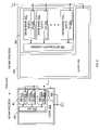
- FIG. 5is a block diagram of an integrated circuit chip 500 fabricated using a 0.13 micron (130 nanometer) process, and a corresponding integrated circuit chip 600 fabricated using a 65 nanometer (nm) process, in accordance with one embodiment of the present invention.
- Integrated circuit chip 500includes embedded DRAM array 501 and logic 502
- integrated circuit chip 600includes embedded DRAM array 601 , logic circuit 602 and voltage boosting circuit 603 .
- Embedded DRAM array 501includes N DRAM banks 510 1 - 510 N , each having a corresponding sense amplifier circuit 520 1 - 520 N , and a memory controller 530 .
- embedded DRAM array 601includes N DRAM banks 610 1 - 610 N , each having a corresponding sense amplifier circuit 620 1 - 620 N , and a memory controller 630 .
- each of DRAM banks 510 1 - 510 N and 610 1 - 610 Nincludes a 32 row by 512 column array of DRAM memory cells.
- DRAM arrays 501 and 601can be implemented using a 32 k ⁇ 32 memory macro similar to the one described in commonly owned U.S. Pat. No. 6,504,780B2, “Method and Apparatus For Completely Hiding Refresh Operations In a DRAM Device Using Clock Division”, by Wingyu Leung.
- Two separate versions of the memory macro using the same memory architecture and memory cell structureare used to design DRAM array 501 and DRAM array 601 .
- an external V CC power supplywhich provides a nominal V CC1 supply voltage of 1.2 Volts, is used to operate sense amplifier circuits 520 1 - 520 N and logic circuit 502 .
- an external V CC power supplywhich provides a reduced nominal V CC2 supply voltage of 1.0 Volts, is used to operate logic circuit 602 .
- Voltage boosting circuit 603generates a boosted voltage V CCS , which is used to operate sense amplifier circuits 620 1 - 620 N .
- the boosted voltage V CCSis selected to be equal to the V CC1 supply voltage of integrated circuit chip 500 (i.e., 1.2 Volts).
- FIG. 6is a block diagram illustrating various device parameters implemented by integrated circuit chips 500 and 600 in accordance with the present embodiment. More specifically, FIG. 6 illustrates: (1) DRAM cells 550 and 650 , which are representative of the DRAM cells included in memory banks 510 1 and 610 1 , respectively; (2) sense amplifier transistors 521 and 621 , which are representative of the transistors implemented by sense amplifier circuits 520 1 and 620 1 , respectively; and (3) logic transistors 512 and 612 , which are representative of the transistors implemented in logic circuits 502 and 602 , respectively.
- DRAM cell 550includes access transistor 551 and cell capacitor 552
- DRAM cell 650includes access transistor 651 and cell capacitor 652 .
- logic transistor 512 and sense amplifier transistor 521each has a gate oxide thickness G OX1 of approximately 20 Angstroms. This thickness is selected to optimize the performance of logic transistor 512 and sense amplifier transistor 521 in response to the V CC1 supply voltage of 1.2 Volts.
- access transistor 551has a gate oxide thickness G OX3 of about 26 Angstroms.
- the thickness of the capacitor oxide C OX of cell capacitor 552has a thickness of about 26 Angstroms.
- these increased oxide thicknessesadvantageously increase the data retention time of DRAM cell 550 .
- cell capacitor 552has a capacitance C C1 of about 3.2 fF.
- DRAM cell 550has a layout area of about 0.52 micron 2 , and an associated bit line capacitance C P1 of about 11 fF.
- logic transistor 612 and sense amplifier transistor 621each has a gate oxide thickness G OX2 of about 16 Angstroms. This thickness is selected to optimize the performance of logic transistor 612 in response to the V CC2 supply voltage of 1.0 Volt.
- the channel length of logic transistor 612corresponds with the minimum line width of the 65 nm process, thereby allowing this transistor to exhibit a fast switching time.
- Sense amplifier transistor 621operates in response to the boosted V CCS voltage of 1.2 Volts. To allow sense amplifier transistor 621 to operate at this higher voltage without reliability degradation, the channel length of this transistor 621 is made longer than the minimum line width of the 65 nm process. For example, sense amplifier transistor 621 may have a channel length of about 90 nm.
- the sense amplifier supply voltage V CCS of 1.2 Voltsis generated by voltage boosting circuit 603 in response to the V CC2 supply voltage of 1.0 Volt.
- the internally generated V CCS voltagehas a much smaller variation (+/ ⁇ 50 mv) than the external V CC2 supply voltage (+/ ⁇ 100 mV). This smaller variation exists because the V CCS voltage is used exclusively to supply the sense amplifier circuits, and because there are only 512 sense amplifier circuits in a memory block (as compared to 1024 or more in a standard DRAM array). Thus, the amount of switching current and consequently the voltage noise is minimized.
- the tighter voltage regulation together with the use of slightly longer channel length in the sense amplifier transistorsallows the use of a higher supply voltage in the sense-amplifier transistors without compromising the reliability of the sense-amplifier circuit.
- access transistor 651has a gate oxide thickness G OX3 of about 26 Angstroms.
- the thickness of the capacitor oxide C OX of cell capacitor 652has a thickness of about 26 Angstroms.
- cell capacitor 652has a capacitance C C2 of about 1.6 fF.
- DRAM cell 650has a layout area of about 0.13 micron 2 , and an associated bit line capacitance C P2 of about 5.5 fF.
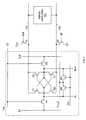
- FIG. 7is a circuit diagram of a sense amplifier 700 used in accordance with one embodiment of the present invention.
- sense amplifier 700may be present in sense amplifier circuit 620 1 of FIG. 6 .
- Sense amplifier 700is similar to the sense amplifier shown in FIG. 1 of commonly owned U.S. Pat. No. 6,324,110 B1, “High-speed Read-write Circuitry For Semi-conductor Memory,” by Wingyu Leung and Jui-Pin Tang, except that sense amplifier uses a sense amplifier power supply voltage V CCS , which is different than the V CC2 supply voltage used by logic circuitry within or outside the memory macro.
- V CCSsense amplifier power supply voltage
- the bi-stable sense-amplifier 700consists of a cross-coupled pair of PMOS transistors P 1 -P 2 and a cross-coupled pair of NMOS transistors N 1 -N 2 .
- the sources of the PMOS cross-coupled pairare connected to the virtual supply line VSL.
- the virtual supply line VSLis common to the other sense amplifiers of the same memory block (e.g., sense amplifier 701 and the other sense amplifiers in sense amplifier circuit 620 1 ).
- the sources of the NMOS cross-coupled pairare connected to the virtual ground line VGL.
- the virtual ground line VGLis common to other sense amplifiers of the same memory block.
- the cross-coupled transistor pairs P 1 -P 2 and N 1 -N 2form a regenerative sense-amplifier, which amplifies the differential signal present on the complementary bit line pair BL and BL#.
- the amplified signal on the bit line pair BL and BL#is coupled to the data line pair DL and DL# through NMOS transistors N 4 and N 5 during a read or write access to the memory block.
- NMOS transistors N 6 and N 7couple bit lines BL and BL#, respectively, to a internally generated voltage which is approximately equal to half of the sense amplifier supply voltage V CCS .
- the gates of transistors N 6 and N 7are coupled to receive the equalization (or pre-charge) control signal EQ.
- the equalization signal EQis activated high, thereby pre-charging the bit lines BL and BL# to V CCS /2.
- the virtual supply line VSLis coupled to the sense amplifier supply voltage V CCS by PMOS transistor P 3 .
- the gate of transistor P 3is coupled to receive sense amplifier enable signal SE#, which is an active low signal.
- the virtual ground line VGLis coupled to the ground voltage supply by NMOS transistor N 3 .
- the gate of transistor N 3is coupled to receive sense amplifier enable signal SE, which is an active high signal (and the complement of SE#).
- the sense amplifier enable signals SE/SE#are activated, and the regenerative latch formed by transistors P 1 -P 2 and N 1 -N 2 amplifies the small sense signal on bit line pair BL/BL#.
- the regenerative latchalso performs data restoration, so that the storage capacitor of the selected DRAM cell is charged substantially close to ground or the V CCS supply voltage at the end of a sensing operation.
- the charge stored in the cell capacitoris directly proportional to the restore voltage. For a logic ‘1’ data value the restored voltage is close to the V CCS sense amplifier supply voltage, and for a logic ‘0’ data value the restored voltage is close to ground.
- the sensing time required for sense amplifier 700 to amplify the sensing voltage (V S ) on bit line pair BL/BL# to the full V CCS voltageis dominated by the initial sensing current in the regenerative latch formed by transistors P 1 -P 2 and N 1 -N 2 when the sense amplifier enable signals SE and SE# are activated.
- This initial sensing currentis proportional to the square of the difference between the bit-line pre-charge voltage V CCS /2 and the absolute threshold voltage (V T ) of the transistors, or (V CCS /2 ⁇ V T ) 2 .
- V CCS /2In sense amplifier 700 (which was fabricated using the 65 nm process), the minimum value of V CCS /2 is 0.575 Volts (i.e., (1.2 Volts ⁇ 50 millivolt variation)/2).
- the absolute threshold voltageis about 0.4 Volts, such that the initial sensing current is equal to 0.03 k, where k is a proportional constant.
- the minimum pre-charge voltagewould be equal to 0.45 Volts (i.e., (1.0 Volt ⁇ 0.1 Volt variation)/2).
- the absolute threshold voltageis about 0.4 Volts, such that the initial sensing current would be equal to 0.0025 k.
- Boosting the sense amplifier supply voltage V SSC to 1.2 Volts in the present embodimenttherefore increases the initial sensing current of sense amplifier 700 by a factor of 12, thereby increasing the sensing speed of sense amplifier 700 .
- the transistors of sense amplifier 700are modified to have an increased gate oxide thickness of 26 Angstroms (i.e., the same thickness as the oxide used in the DRAM cells).
- the channel lengths of the transistor gatesare all increased to 0.18 microns.
- the longer gate lengths and the increased gate oxide thicknessallow sense amplifier supply voltage V CCS to be increased to 2.0 Volts, without compromising the long-term reliability of the sense amplifier 700 .
- Increasing the channel length of the transistors to 0.18 micronsincreases the overall layout area of sense amplifier 700 by less than 10 percent because the layout area is dominated by interconnect structures associated with the transistors and the channel widths of these transistors, which have dimensions substantially greater than 0.18 microns.
- a sense amplifier supply voltage V CCS of 2.0 Voltsallows 67 percent more charge to be stored in the DRAM cell capacitor than a sense amplifier supply voltage V CCS of 1.2 Volts. As a result, the cell capacitance of the memory cell can be reduced by 67 percent without affecting the sensing voltage V S .
- the folded capacitor shown in FIG. 4includes both a planar component and a side-wall component.
- the side-wall component dimensionis limited by the minimum lateral design rules and the trench depth of the process. Therefore, side-wall capacitance cannot be reduced further.
- the planar componentcan be reduced to design rules minimum. This results in a cell size reduction of less than 10 percent, because the lateral dimension of the original cell capacitor is already quite close the design rule limit.
- the benefit of this schemeis more prominent if a planar capacitor structure is used instead of trench or stack capacitor structure. This is because, as illustrated in FIG. 2 , when using a planar capacitor structure, the cell size is pre-dominantly occupied by the lateral storage capacitance.
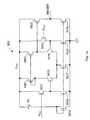
- FIG. 8is a circuit diagram of a voltage translation circuit 800 that can be used for this purpose.
- Voltage translation circuit 800which includes PMOS transistors 801 - 802 , NMOS transistors 803 - 804 and inverter 805 , generates the sense amplifier enable signals SE/SE# in response to a SENSE logic signal, which has a voltage swing of V CC2 to 0.
- the equalization signal EQ and column select signal CScan be generated in a similar manner. Because voltage translation is well known in the art of memory and logic design, this circuit is not elaborated further in this disclosure.
- voltage boosting circuit 603( FIG. 6 ) is a charge pump regulator, which generates the sense-amplifier supply voltage V CCS of 1.2 Volts in response to the 1 Volt external power supply V CC2 .
- Charge pump regulatorsare well known in the art.
- FIG. 9is a block diagram of a boosted voltage generator 603 used in one embodiment of the present invention.
- Boosted voltage generator 603includes a ring oscillator 901 , a charge pump 902 and a voltage comparator 903 , which compares the output voltage V CCS of the generator with a reference voltage V REF .
- Ring oscillator 901 and charge pump 902are conventional elements that are well documented in references such as U.S. Pat. Nos. 5,703,827 and 5,267,201.
- the reference voltage V REFcan be generated external to the memory using a band-gap reference circuit such as those described in “Analysis and Design of Analog Integrated Circuits”, by P. R. Gray and R. G. Meyer, John Wiley and Sons Inc. 3 rd edition, 1993, pp. 338-346.
- FIG. 10is a circuit diagram of voltage comparator 903 , as used in one embodiment of the present invention.
- Voltage comparator 903includes PMOS transistors 1001 - 1003 , NMOS transistors 1011 - 1019 and resistor R 1 .
- Transistors 1001 - 1003 and 1015 - 1018form a conventional two-stage differential amplifier, which amplifies the differential signal applied to the gates of transistors 1015 and 1016 .
- the small differential signalis amplified and converted into a full swing digital output signal, INHIBIT. Because the voltages V REF and V CCS received by comparator 903 are normally greater than V CC2 , a voltage step down circuit is used to ensure that the two stage amplifier stays in a high gain operating region.
- Transistors 1011 - 1014form a source-follower that translates both the reference voltage V REF and sense amplifier supply voltage V CCS to values about one threshold voltage drop (V T ⁇ 0.4 Volts) lower than their respective values.
- Resistor R 1 and transistor 1019form a biasing circuit setting transistors 1013 , 1014 , 1017 and 1018 in the saturation region.
- the V CCS voltagecan be regulated with high precision. Because the loading on the V CCS voltage supply is minimized by using a small bank size, with a relatively small number of sense amplifiers turning on at one time, the switching noise amplitude is minimized.
Landscapes
- Engineering & Computer Science (AREA)
- Microelectronics & Electronic Packaging (AREA)
- Computer Hardware Design (AREA)
- Power Engineering (AREA)
- Dram (AREA)
- Semiconductor Memories (AREA)
Abstract
Description
VS=VCC(CC)/[2(CC+CP)] (1)
VS=VCC(CC)/2CP (2)
VS=k(CC) (3)
VS=VCCS(CC)/2CP (4)
Because VCCSis constant, equation (4) can be simplified as follows (where K is a constant).
VS=K(CC)/CP (5)
Q=VCCS*CC/2 (6)
Claims (18)
Priority Applications (1)
| Application Number | Priority Date | Filing Date | Title |
|---|---|---|---|
| US12/048,170US7791975B2 (en) | 2005-06-24 | 2008-03-13 | Scalable embedded DRAM array |
Applications Claiming Priority (3)
| Application Number | Priority Date | Filing Date | Title |
|---|---|---|---|
| US11/166,856US7274618B2 (en) | 2005-06-24 | 2005-06-24 | Word line driver for DRAM embedded in a logic process |
| US11/534,506US7499307B2 (en) | 2005-06-24 | 2006-09-22 | Scalable embedded DRAM array |
| US12/048,170US7791975B2 (en) | 2005-06-24 | 2008-03-13 | Scalable embedded DRAM array |
Related Parent Applications (1)
| Application Number | Title | Priority Date | Filing Date |
|---|---|---|---|
| US11/534,506DivisionUS7499307B2 (en) | 2005-06-24 | 2006-09-22 | Scalable embedded DRAM array |
Publications (2)
| Publication Number | Publication Date |
|---|---|
| US20080159036A1 US20080159036A1 (en) | 2008-07-03 |
| US7791975B2true US7791975B2 (en) | 2010-09-07 |
Family
ID=39201233
Family Applications (3)
| Application Number | Title | Priority Date | Filing Date |
|---|---|---|---|
| US11/534,506Expired - LifetimeUS7499307B2 (en) | 2005-06-24 | 2006-09-22 | Scalable embedded DRAM array |
| US12/048,170Active2026-02-25US7791975B2 (en) | 2005-06-24 | 2008-03-13 | Scalable embedded DRAM array |
| US12/048,176Expired - Fee RelatedUS7684229B2 (en) | 2005-06-24 | 2008-03-13 | Scalable embedded DRAM array |
Family Applications Before (1)
| Application Number | Title | Priority Date | Filing Date |
|---|---|---|---|
| US11/534,506Expired - LifetimeUS7499307B2 (en) | 2005-06-24 | 2006-09-22 | Scalable embedded DRAM array |
Family Applications After (1)
| Application Number | Title | Priority Date | Filing Date |
|---|---|---|---|
| US12/048,176Expired - Fee RelatedUS7684229B2 (en) | 2005-06-24 | 2008-03-13 | Scalable embedded DRAM array |
Country Status (5)
| Country | Link |
|---|---|
| US (3) | US7499307B2 (en) |
| JP (1) | JP5563302B2 (en) |
| KR (1) | KR20090057263A (en) |
| TW (1) | TWI492228B (en) |
| WO (1) | WO2008036729A2 (en) |
Cited By (1)
| Publication number | Priority date | Publication date | Assignee | Title |
|---|---|---|---|---|
| TWI809818B (en)* | 2021-04-14 | 2023-07-21 | 鈺創科技股份有限公司 | Dynamic memory with sustainable storage architecture and clean up circuit |
Families Citing this family (15)
| Publication number | Priority date | Publication date | Assignee | Title |
|---|---|---|---|---|
| KR100752669B1 (en)* | 2006-08-22 | 2007-08-29 | 삼성전자주식회사 | Bitline Sense Amplifier in Semiconductor Memory Device with Open Bitline Structure |
| JP2009123272A (en)* | 2007-11-14 | 2009-06-04 | Nec Electronics Corp | Semiconductor memory and its control method |
| KR101194896B1 (en)* | 2010-08-30 | 2012-10-25 | 에스케이하이닉스 주식회사 | Nonvolatile memory device |
| US8780614B2 (en)* | 2011-02-02 | 2014-07-15 | Semiconductor Energy Laboratory Co., Ltd. | Semiconductor memory device |
| US8743591B2 (en)* | 2011-04-26 | 2014-06-03 | Semiconductor Energy Laboratory Co., Ltd. | Semiconductor memory device and method for driving the same |
| US8705282B2 (en)* | 2011-11-01 | 2014-04-22 | Silicon Storage Technology, Inc. | Mixed voltage non-volatile memory integrated circuit with power saving |
| US9105351B2 (en)* | 2011-11-09 | 2015-08-11 | Semiconductor Energy Laboratory Co., Ltd. | Semiconductor memory device including amplifier circuit |
| WO2018186835A1 (en)* | 2017-04-04 | 2018-10-11 | Intel Corporation | Thin-film transistor embedded dynamic random-access memory |
| US10026740B1 (en) | 2017-10-30 | 2018-07-17 | Globalfoundries Inc. | DRAM structure with a single diffusion break |
| US12354646B2 (en) | 2018-12-10 | 2025-07-08 | Etron Technology, Inc. | Dynamic memory with sustainable storage architecture |
| US12361998B2 (en) | 2018-12-10 | 2025-07-15 | Invention And Collaboration Laboratory Pte. Ltd. | Sustainable DRAM having principle power supply voltage unified with logic circuit |
| US12068020B2 (en) | 2018-12-10 | 2024-08-20 | Etron Technology, Inc. | Dynamic memory with sustainable storage architecture and clean up circuit |
| US10984874B1 (en)* | 2019-11-13 | 2021-04-20 | Sandisk Technologies Llc | Differential dbus scheme for low-latency random read for NAND memories |
| JP7486545B2 (en)* | 2021-05-28 | 2024-05-17 | ▲ゆ▼創科技股▲ふん▼有限公司 | Sustainable DRAM with a unified main power supply voltage for logic circuits |
| TW202401681A (en)* | 2022-01-27 | 2024-01-01 | 新加坡商發明與合作實驗室有限公司 | Integrated scaling and stretching platform for server processor and rack server unit |
Citations (59)
| Publication number | Priority date | Publication date | Assignee | Title |
|---|---|---|---|---|
| US4446536A (en) | 1982-06-21 | 1984-05-01 | Mcdonnell Douglas Corporation | Complementary metal oxide semiconductors address drive circuit |
| US5365479A (en) | 1994-03-03 | 1994-11-15 | National Semiconductor Corp. | Row decoder and driver with switched-bias bulk regions |
| US5438543A (en) | 1993-04-06 | 1995-08-01 | Samsung Electronics Co., Ltd. | Semiconductor memory using low power supply voltage |
| US5719814A (en) | 1995-10-31 | 1998-02-17 | Nec Corporation | Semiconductor memory device capable of storing high potential level of data |
| US5822252A (en) | 1996-03-29 | 1998-10-13 | Aplus Integrated Circuits, Inc. | Flash memory wordline decoder with overerase repair |
| US5846860A (en) | 1996-06-24 | 1998-12-08 | Taiwan Semiconductor Manufacturing Company, Ltd. | Method of making buried contact in DRAM technology |
| US5917766A (en) | 1996-05-28 | 1999-06-29 | Mitsubishi Denki Kabushiki Kaisha | Semiconductor memory device that can carry out read disturb testing and burn-in testing reliably |
| US5920225A (en) | 1995-12-20 | 1999-07-06 | Hyundai Electronic Industries, Co., Ltd. | Negative voltage drive circuit |
| US5963477A (en) | 1997-12-09 | 1999-10-05 | Macronix International Co., Ltd. | Flash EPROM erase algorithm with wordline level retry |
| US6028804A (en) | 1998-03-09 | 2000-02-22 | Monolithic System Technology, Inc. | Method and apparatus for 1-T SRAM compatible memory |
| US6031779A (en) | 1997-04-10 | 2000-02-29 | Hitachi, Ltd. | Dynamic memory |
| US6043536A (en) | 1998-05-19 | 2000-03-28 | Kabushiki Kaisha Toshiba | Semiconductor device |
| US6075720A (en) | 1998-08-14 | 2000-06-13 | Monolithic System Tech Inc | Memory cell for DRAM embedded in logic |
| US6088267A (en) | 1991-07-25 | 2000-07-11 | Kabushiki Kaisha Toshiba | Nonvolatile semiconductor memory device having row decoder |
| US6140175A (en)* | 1999-03-03 | 2000-10-31 | International Business Machines Corporation | Self-aligned deep trench DRAM array device |
| US6147914A (en) | 1998-08-14 | 2000-11-14 | Monolithic System Technology, Inc. | On-chip word line voltage generation for DRAM embedded in logic process |
| US6187618B1 (en) | 1997-06-02 | 2001-02-13 | Micron Technology, Inc. | Vertical bipolar SRAM cell, array and system, and a method for making the cell and the array |
| US6190988B1 (en)* | 1998-05-28 | 2001-02-20 | International Business Machines Corporation | Method for a controlled bottle trench for a dram storage node |
| US20010014045A1 (en) | 2000-02-16 | 2001-08-16 | Fujitsu Limited | Memory circuit for preventing rise cell array power source |
| US20010053093A1 (en) | 2000-02-16 | 2001-12-20 | Halo Lsi Device & Design Technology Inc. | Wordline decoder for flash memory |
| US20020011883A1 (en) | 2000-07-26 | 2002-01-31 | Mitsubishi Denki Kabushiki Kaisha, And Mitsubishi Electric Engineering Company Limited | Multi-power semiconductor integrated circuit device |
| US20020017947A1 (en) | 1998-11-17 | 2002-02-14 | Mitsubishi Denki Kabushiki Kaisha | Semiconductor circuit device having hierarchical power supply structure |
| US20020041531A1 (en) | 1997-06-16 | 2002-04-11 | Hitoshi Tanaka | Semiconductor integrated circuit device |
| US20020076880A1 (en) | 2000-06-12 | 2002-06-20 | Takashi Yamada | Semiconductor device and method of fabricating the same |
| US20020097628A1 (en) | 1998-04-09 | 2002-07-25 | Hiroki Fujisawa | Semiconductor integrated circuit device |
| US6440801B1 (en) | 1997-01-22 | 2002-08-27 | International Business Machines Corporation | Structure for folded architecture pillar memory cell |
| US20020122344A1 (en) | 2001-03-01 | 2002-09-05 | Riichiro Takemura | Sense amplifiers having reduced Vth deviation |
| US6455901B2 (en) | 2000-03-30 | 2002-09-24 | Kabushiki Kaisha Toshiba | Semiconductor integrated circuit |
| US6473344B2 (en) | 2001-01-03 | 2002-10-29 | Samsung Electronics Co., Ltd. | Semiconductor memory device capable of outputting a wordline voltage via an external pin |
| US6493268B1 (en) | 2000-07-13 | 2002-12-10 | Stmicroelectronics S.R.L. | Circuit device for performing hierarchic row decoding in non-volatile memory devices |
| US6496034B2 (en) | 2001-02-09 | 2002-12-17 | Micron Technology, Inc. | Programmable logic arrays with ultra thin body transistors |
| US20030001181A1 (en) | 1998-08-14 | 2003-01-02 | Monolithic System Technology, Inc. | Method of fabricating a DRAM cell having a thin dielectric access transistor and a thick dielectric storage capacitor |
| US20030002353A1 (en) | 2001-06-30 | 2003-01-02 | Jae-Goo Lee | Integrated circuit memory devices having sense amplifiers therein that receive nominal and boosted supply voltages when active and methods of operating same |
| US20030058722A1 (en) | 2001-09-24 | 2003-03-27 | San-Ha Park | Semiconductor memory device and method for driving a sense amplifier |
| US6549465B2 (en) | 2001-02-28 | 2003-04-15 | Sharp Kabushiki Kaisha | Nonvolatile semiconductor memory well voltage setting circuit without latchup and semiconductor memory device provided with the circuit |
| US6573548B2 (en) | 1998-08-14 | 2003-06-03 | Monolithic System Technology, Inc. | DRAM cell having a capacitor structure fabricated partially in a cavity and method for operating same |
| US6600186B1 (en) | 1998-11-19 | 2003-07-29 | Taiwan Semiconductor Manufacturing Company | Process technology architecture of embedded DRAM |
| US20030148580A1 (en)* | 2002-02-05 | 2003-08-07 | Nanya Technology Corporation | Method of forming a bottle-shaped trench in a semiconductor substrate |
| US20030185085A1 (en) | 2002-03-26 | 2003-10-02 | Tetsuya Kaneko | Memory embedded logic integrated circuit mounting memory circuits having different performances on the same ship |
| US20030223261A1 (en) | 2002-05-29 | 2003-12-04 | Fujitsu Limited | Semiconductor memory device |
| US6661699B1 (en) | 1998-02-02 | 2003-12-09 | Darryl Gene Walker | Random access memory cell having double-gate access transistor for reduced leakage current |
| US6665851B1 (en) | 2001-12-04 | 2003-12-16 | Synopsys, Inc. | Quick placement of electronic circuits using orthogonal one dimensional placements |
| US6718431B2 (en) | 1997-10-10 | 2004-04-06 | Rambus Inc. | Apparatus and method for pipelined memory operations |
| US20040085835A1 (en) | 2002-10-29 | 2004-05-06 | Jin-Hong Ahn | Semiconductor memory device with reduced data access time |
| US6865114B2 (en) | 2002-02-20 | 2005-03-08 | Stmicroelectronics, S.R.L. | Word line selector for a semiconductor memory |
| US20050068838A1 (en) | 2003-09-26 | 2005-03-31 | Renesas Technology Corp. | Semiconductor memory device allowing accurate burn-in test |
| US20050117411A1 (en) | 2003-11-28 | 2005-06-02 | Elpida Memory, Inc. | Semiconductor storage device |
| US20050174873A1 (en) | 2003-05-13 | 2005-08-11 | Richard Ferrant | Semiconductor memory device and method of operating same |
| US6930927B2 (en) | 2002-07-10 | 2005-08-16 | Stmicroelectronics S.R.L. | Line selector for a matrix of memory elements |
| US6940759B2 (en) | 2003-10-14 | 2005-09-06 | Atmel Corporation | Group erasing system for flash array with multiple sectors |
| US20050208727A1 (en) | 2004-03-18 | 2005-09-22 | Nanya Technology Corporation | Method of etching bottle trench and fabricating capacitor with same |
| US20050280061A1 (en) | 2004-06-21 | 2005-12-22 | Sang-Yun Lee | Vertical memory device structures |
| US20060007612A1 (en) | 2004-07-06 | 2006-01-12 | Saifun Semiconductors, Ltd. | Protection of NROM devices from charge damage |
| USRE38944E1 (en) | 1994-12-20 | 2006-01-24 | Hitachi, Ltd. | Semiconductor memory |
| US7020024B2 (en) | 2002-04-04 | 2006-03-28 | Samsung Electronics Co., Ltd. | Methods and devices for increasing voltages on non-selected wordlines during erasure of a flash memory |
| US20060112321A1 (en) | 2004-11-23 | 2006-05-25 | Monolithic System Technology, Inc. | Transparent error correcting memory that supports partial-word write |
| US20060172504A1 (en) | 2005-02-03 | 2006-08-03 | Monolithic System Technology, Inc. | Fabrication process for increased capacitance in an embedded DRAM memory |
| US20060273848A1 (en) | 2003-05-13 | 2006-12-07 | Fujitsu Limited | Semiconductor integrated circuit device |
| US20080288188A1 (en) | 2007-05-17 | 2008-11-20 | Chang William Y | Structure and Method for Monitoring Variation Within an Active Region of a Semiconductor Device Using Scaling |
Family Cites Families (10)
| Publication number | Priority date | Publication date | Assignee | Title |
|---|---|---|---|---|
| JP2647948B2 (en)* | 1989-02-02 | 1997-08-27 | 松下電器産業株式会社 | Semiconductor memory device |
| JPH0828476B2 (en)* | 1991-06-07 | 1996-03-21 | 富士通株式会社 | Semiconductor device and manufacturing method thereof |
| JPH0778472A (en)* | 1993-09-10 | 1995-03-20 | Toshiba Corp | Semiconductor integrated circuit |
| JP3510335B2 (en)* | 1994-07-18 | 2004-03-29 | 株式会社ルネサステクノロジ | Semiconductor memory device, internal power supply voltage generation circuit, internal high voltage generation circuit, intermediate voltage generation circuit, constant current source, and reference voltage generation circuit |
| KR100335496B1 (en)* | 1999-11-26 | 2002-05-08 | 윤종용 | Internal voltage generation circuit that can operate safely under low power voltage VCC |
| JP2002083942A (en)* | 2000-09-06 | 2002-03-22 | Matsushita Electric Ind Co Ltd | Semiconductor integrated circuit device |
| JP2002343083A (en)* | 2001-05-18 | 2002-11-29 | Mitsubishi Electric Corp | Semiconductor device |
| JP2003283321A (en)* | 2002-03-27 | 2003-10-03 | Mitsubishi Electric Corp | Internal power supply potential generation circuit |
| JP2005322380A (en)* | 2004-04-09 | 2005-11-17 | Toshiba Corp | Semiconductor memory device |
| US7363601B2 (en)* | 2004-10-15 | 2008-04-22 | International Business Machines Corporation | Integrated circuit selective scaling |
- 2006
- 2006-09-22USUS11/534,506patent/US7499307B2/ennot_activeExpired - Lifetime
- 2007
- 2007-08-01TWTW096128309Apatent/TWI492228B/ennot_activeIP Right Cessation
- 2007-09-19WOPCT/US2007/078878patent/WO2008036729A2/enactiveApplication Filing
- 2007-09-19JPJP2009529360Apatent/JP5563302B2/ennot_activeExpired - Fee Related
- 2007-09-19KRKR1020097005777Apatent/KR20090057263A/ennot_activeWithdrawn
- 2008
- 2008-03-13USUS12/048,170patent/US7791975B2/enactiveActive
- 2008-03-13USUS12/048,176patent/US7684229B2/ennot_activeExpired - Fee Related
Patent Citations (61)
| Publication number | Priority date | Publication date | Assignee | Title |
|---|---|---|---|---|
| US4446536A (en) | 1982-06-21 | 1984-05-01 | Mcdonnell Douglas Corporation | Complementary metal oxide semiconductors address drive circuit |
| US6166987A (en) | 1991-07-25 | 2000-12-26 | Kabushiki Kaisha Toshiba | Nonvolatile semiconductor memory device having row decoder |
| US6088267A (en) | 1991-07-25 | 2000-07-11 | Kabushiki Kaisha Toshiba | Nonvolatile semiconductor memory device having row decoder |
| US5438543A (en) | 1993-04-06 | 1995-08-01 | Samsung Electronics Co., Ltd. | Semiconductor memory using low power supply voltage |
| US5365479A (en) | 1994-03-03 | 1994-11-15 | National Semiconductor Corp. | Row decoder and driver with switched-bias bulk regions |
| USRE38944E1 (en) | 1994-12-20 | 2006-01-24 | Hitachi, Ltd. | Semiconductor memory |
| US5719814A (en) | 1995-10-31 | 1998-02-17 | Nec Corporation | Semiconductor memory device capable of storing high potential level of data |
| US5920225A (en) | 1995-12-20 | 1999-07-06 | Hyundai Electronic Industries, Co., Ltd. | Negative voltage drive circuit |
| US5822252A (en) | 1996-03-29 | 1998-10-13 | Aplus Integrated Circuits, Inc. | Flash memory wordline decoder with overerase repair |
| US5917766A (en) | 1996-05-28 | 1999-06-29 | Mitsubishi Denki Kabushiki Kaisha | Semiconductor memory device that can carry out read disturb testing and burn-in testing reliably |
| US5846860A (en) | 1996-06-24 | 1998-12-08 | Taiwan Semiconductor Manufacturing Company, Ltd. | Method of making buried contact in DRAM technology |
| US6440801B1 (en) | 1997-01-22 | 2002-08-27 | International Business Machines Corporation | Structure for folded architecture pillar memory cell |
| US6031779A (en) | 1997-04-10 | 2000-02-29 | Hitachi, Ltd. | Dynamic memory |
| US6187618B1 (en) | 1997-06-02 | 2001-02-13 | Micron Technology, Inc. | Vertical bipolar SRAM cell, array and system, and a method for making the cell and the array |
| US20020041531A1 (en) | 1997-06-16 | 2002-04-11 | Hitoshi Tanaka | Semiconductor integrated circuit device |
| US6718431B2 (en) | 1997-10-10 | 2004-04-06 | Rambus Inc. | Apparatus and method for pipelined memory operations |
| US5963477A (en) | 1997-12-09 | 1999-10-05 | Macronix International Co., Ltd. | Flash EPROM erase algorithm with wordline level retry |
| US6661699B1 (en) | 1998-02-02 | 2003-12-09 | Darryl Gene Walker | Random access memory cell having double-gate access transistor for reduced leakage current |
| US6028804A (en) | 1998-03-09 | 2000-02-22 | Monolithic System Technology, Inc. | Method and apparatus for 1-T SRAM compatible memory |
| US20020097628A1 (en) | 1998-04-09 | 2002-07-25 | Hiroki Fujisawa | Semiconductor integrated circuit device |
| US6043536A (en) | 1998-05-19 | 2000-03-28 | Kabushiki Kaisha Toshiba | Semiconductor device |
| US6190988B1 (en)* | 1998-05-28 | 2001-02-20 | International Business Machines Corporation | Method for a controlled bottle trench for a dram storage node |
| US20030001181A1 (en) | 1998-08-14 | 2003-01-02 | Monolithic System Technology, Inc. | Method of fabricating a DRAM cell having a thin dielectric access transistor and a thick dielectric storage capacitor |
| US20030151072A1 (en) | 1998-08-14 | 2003-08-14 | Monolithic System Technology, Inc. | DRAM cell having a capacitor structure fabricated partially in a cavity and method for operating same |
| US6147914A (en) | 1998-08-14 | 2000-11-14 | Monolithic System Technology, Inc. | On-chip word line voltage generation for DRAM embedded in logic process |
| US6075720A (en) | 1998-08-14 | 2000-06-13 | Monolithic System Tech Inc | Memory cell for DRAM embedded in logic |
| US6573548B2 (en) | 1998-08-14 | 2003-06-03 | Monolithic System Technology, Inc. | DRAM cell having a capacitor structure fabricated partially in a cavity and method for operating same |
| US20020017947A1 (en) | 1998-11-17 | 2002-02-14 | Mitsubishi Denki Kabushiki Kaisha | Semiconductor circuit device having hierarchical power supply structure |
| US6600186B1 (en) | 1998-11-19 | 2003-07-29 | Taiwan Semiconductor Manufacturing Company | Process technology architecture of embedded DRAM |
| US6140175A (en)* | 1999-03-03 | 2000-10-31 | International Business Machines Corporation | Self-aligned deep trench DRAM array device |
| US20010014045A1 (en) | 2000-02-16 | 2001-08-16 | Fujitsu Limited | Memory circuit for preventing rise cell array power source |
| US20010053093A1 (en) | 2000-02-16 | 2001-12-20 | Halo Lsi Device & Design Technology Inc. | Wordline decoder for flash memory |
| US6455901B2 (en) | 2000-03-30 | 2002-09-24 | Kabushiki Kaisha Toshiba | Semiconductor integrated circuit |
| US20020076880A1 (en) | 2000-06-12 | 2002-06-20 | Takashi Yamada | Semiconductor device and method of fabricating the same |
| US6493268B1 (en) | 2000-07-13 | 2002-12-10 | Stmicroelectronics S.R.L. | Circuit device for performing hierarchic row decoding in non-volatile memory devices |
| US20020011883A1 (en) | 2000-07-26 | 2002-01-31 | Mitsubishi Denki Kabushiki Kaisha, And Mitsubishi Electric Engineering Company Limited | Multi-power semiconductor integrated circuit device |
| US6473344B2 (en) | 2001-01-03 | 2002-10-29 | Samsung Electronics Co., Ltd. | Semiconductor memory device capable of outputting a wordline voltage via an external pin |
| US6496034B2 (en) | 2001-02-09 | 2002-12-17 | Micron Technology, Inc. | Programmable logic arrays with ultra thin body transistors |
| US6549465B2 (en) | 2001-02-28 | 2003-04-15 | Sharp Kabushiki Kaisha | Nonvolatile semiconductor memory well voltage setting circuit without latchup and semiconductor memory device provided with the circuit |
| US20020122344A1 (en) | 2001-03-01 | 2002-09-05 | Riichiro Takemura | Sense amplifiers having reduced Vth deviation |
| US20030002353A1 (en) | 2001-06-30 | 2003-01-02 | Jae-Goo Lee | Integrated circuit memory devices having sense amplifiers therein that receive nominal and boosted supply voltages when active and methods of operating same |
| US20030058722A1 (en) | 2001-09-24 | 2003-03-27 | San-Ha Park | Semiconductor memory device and method for driving a sense amplifier |
| US6665851B1 (en) | 2001-12-04 | 2003-12-16 | Synopsys, Inc. | Quick placement of electronic circuits using orthogonal one dimensional placements |
| US20030148580A1 (en)* | 2002-02-05 | 2003-08-07 | Nanya Technology Corporation | Method of forming a bottle-shaped trench in a semiconductor substrate |
| US6865114B2 (en) | 2002-02-20 | 2005-03-08 | Stmicroelectronics, S.R.L. | Word line selector for a semiconductor memory |
| US20030185085A1 (en) | 2002-03-26 | 2003-10-02 | Tetsuya Kaneko | Memory embedded logic integrated circuit mounting memory circuits having different performances on the same ship |
| US7020024B2 (en) | 2002-04-04 | 2006-03-28 | Samsung Electronics Co., Ltd. | Methods and devices for increasing voltages on non-selected wordlines during erasure of a flash memory |
| US20030223261A1 (en) | 2002-05-29 | 2003-12-04 | Fujitsu Limited | Semiconductor memory device |
| US6930927B2 (en) | 2002-07-10 | 2005-08-16 | Stmicroelectronics S.R.L. | Line selector for a matrix of memory elements |
| US20040085835A1 (en) | 2002-10-29 | 2004-05-06 | Jin-Hong Ahn | Semiconductor memory device with reduced data access time |
| US20060273848A1 (en) | 2003-05-13 | 2006-12-07 | Fujitsu Limited | Semiconductor integrated circuit device |
| US20050174873A1 (en) | 2003-05-13 | 2005-08-11 | Richard Ferrant | Semiconductor memory device and method of operating same |
| US20050068838A1 (en) | 2003-09-26 | 2005-03-31 | Renesas Technology Corp. | Semiconductor memory device allowing accurate burn-in test |
| US6940759B2 (en) | 2003-10-14 | 2005-09-06 | Atmel Corporation | Group erasing system for flash array with multiple sectors |
| US20050117411A1 (en) | 2003-11-28 | 2005-06-02 | Elpida Memory, Inc. | Semiconductor storage device |
| US20050208727A1 (en) | 2004-03-18 | 2005-09-22 | Nanya Technology Corporation | Method of etching bottle trench and fabricating capacitor with same |
| US20050280061A1 (en) | 2004-06-21 | 2005-12-22 | Sang-Yun Lee | Vertical memory device structures |
| US20060007612A1 (en) | 2004-07-06 | 2006-01-12 | Saifun Semiconductors, Ltd. | Protection of NROM devices from charge damage |
| US20060112321A1 (en) | 2004-11-23 | 2006-05-25 | Monolithic System Technology, Inc. | Transparent error correcting memory that supports partial-word write |
| US20060172504A1 (en) | 2005-02-03 | 2006-08-03 | Monolithic System Technology, Inc. | Fabrication process for increased capacitance in an embedded DRAM memory |
| US20080288188A1 (en) | 2007-05-17 | 2008-11-20 | Chang William Y | Structure and Method for Monitoring Variation Within an Active Region of a Semiconductor Device Using Scaling |
Non-Patent Citations (3)
| Title |
|---|
| "A 1-Mbit CMOS Dynamic RAM with a Divided Bitline Matrix Architecture", pp. 894-902, IEEE Journal of Solid-State Circuits, vol. SC-20, No. 5, Oct. 1985 by R. Taylor et al. |
| "A Mechanically Enhanced Storage node for virtually unlimited Height (MESH) Capacitor Aiming at sub 70mm DRAMs", 4 pgs., 2004, by D.H. Kim et al. |
| "Dual-Operating-Voltage Scheme for a Single 5-V 16-Mbit DRAM", pp. 1128, 1130 & 1132; IEEE Journal of Solid-State Circuits, vol. 23, No. 5, Oct. 1988, by M. Horiguchi et al. |
Cited By (1)
| Publication number | Priority date | Publication date | Assignee | Title |
|---|---|---|---|---|
| TWI809818B (en)* | 2021-04-14 | 2023-07-21 | 鈺創科技股份有限公司 | Dynamic memory with sustainable storage architecture and clean up circuit |
Also Published As
| Publication number | Publication date |
|---|---|
| JP2010504602A (en) | 2010-02-12 |
| US20070070759A1 (en) | 2007-03-29 |
| TW200816198A (en) | 2008-04-01 |
| WO2008036729A3 (en) | 2008-05-15 |
| KR20090057263A (en) | 2009-06-04 |
| US7499307B2 (en) | 2009-03-03 |
| US7684229B2 (en) | 2010-03-23 |
| WO2008036729A2 (en) | 2008-03-27 |
| US20080158929A1 (en) | 2008-07-03 |
| US20080159036A1 (en) | 2008-07-03 |
| TWI492228B (en) | 2015-07-11 |
| JP5563302B2 (en) | 2014-07-30 |
Similar Documents
| Publication | Publication Date | Title |
|---|---|---|
| US7791975B2 (en) | Scalable embedded DRAM array | |
| US7447104B2 (en) | Word line driver for DRAM embedded in a logic process | |
| US6798686B2 (en) | Semiconductor device | |
| KR100351594B1 (en) | Ferroelectric memory and semiconductor memory | |
| US20160284711A1 (en) | Semiconductor memory device and method for driving the same | |
| US20070025162A1 (en) | Sram cell with column select line | |
| US20100277996A1 (en) | Semiconductor device | |
| US7613024B2 (en) | Local digit line architecture and method for memory devices having multi-bit or low capacitance memory cells | |
| US5255235A (en) | Dynamic random access memory with dummy word lines connected to bit line potential adjusting capacitors | |
| US7233536B2 (en) | Semiconductor memory device having memory cells to store cell data and reference data | |
| US4982367A (en) | Dynamic random access memory with well-balanced read-out voltage on bit line pair and operating method therefor | |
| US7035128B2 (en) | Semiconductor memory device and semiconductor integrated circuit device | |
| CN1965404A (en) | Semiconductor storage | |
| US7038943B2 (en) | Memory array having 2T memory cells | |
| US6549448B2 (en) | FeRAM having adjacent memory cells sharing cell plate and driving method for the same | |
| US6271557B1 (en) | Center node for deep trench capacitors | |
| JPH10302464A (en) | Semiconductor integrated circuit and its power supply voltage step-down circuit | |
| Itoh et al. | Central Research Laboratory, Hitachi Ltd., Kokubunji-shi, Tokyo 185, Japan* Hitachi Cambridge Laboratory, Hitachi Europe Ltd., Cavendish Laboratory | |
| JPH07192456A (en) | Semiconductor memory device |
Legal Events
| Date | Code | Title | Description |
|---|---|---|---|
| AS | Assignment | Owner name:MOSYS, INC., CALIFORNIA Free format text:CHANGE OF NAME;ASSIGNOR:MONOLITHIC SYSTEM TECHNOLOGY, INC.;REEL/FRAME:020741/0975 Effective date:20060525 Owner name:MOSYS, INC.,CALIFORNIA Free format text:CHANGE OF NAME;ASSIGNOR:MONOLITHIC SYSTEM TECHNOLOGY, INC.;REEL/FRAME:020741/0975 Effective date:20060525 | |
| STCF | Information on status: patent grant | Free format text:PATENTED CASE | |
| FPAY | Fee payment | Year of fee payment:4 | |
| AS | Assignment | Owner name:INGALLS & SNYDER LLC, NEW YORK Free format text:SECURITY INTEREST;ASSIGNOR:MOSYS, INC.;REEL/FRAME:038081/0262 Effective date:20160314 | |
| MAFP | Maintenance fee payment | Free format text:PAYMENT OF MAINTENANCE FEE, 8TH YEAR, LARGE ENTITY (ORIGINAL EVENT CODE: M1552) Year of fee payment:8 | |
| MAFP | Maintenance fee payment | Free format text:PAYMENT OF MAINTENANCE FEE, 12TH YEAR, LARGE ENTITY (ORIGINAL EVENT CODE: M1553); ENTITY STATUS OF PATENT OWNER: LARGE ENTITY Year of fee payment:12 | |
| AS | Assignment | Owner name:INGALLS & SNYDER LLC, NEW YORK Free format text:RELEASE BY SECURED PARTY;ASSIGNOR:PERASO INC. F/K/A MOSYS, INC.;REEL/FRAME:061593/0094 Effective date:20221003 |