US7791925B2 - Structures for resistive random access memory cells - Google Patents
Structures for resistive random access memory cellsDownload PDFInfo
- Publication number
- US7791925B2 US7791925B2US12/262,262US26226208AUS7791925B2US 7791925 B2US7791925 B2US 7791925B2US 26226208 AUS26226208 AUS 26226208AUS 7791925 B2US7791925 B2US 7791925B2
- Authority
- US
- United States
- Prior art keywords
- electrode
- rram
- random access
- access memory
- resistive
- Prior art date
- Legal status (The legal status is an assumption and is not a legal conclusion. Google has not performed a legal analysis and makes no representation as to the accuracy of the status listed.)
- Active, expires
Links
Images


Classifications
- G—PHYSICS
- G11—INFORMATION STORAGE
- G11C—STATIC STORES
- G11C13/00—Digital stores characterised by the use of storage elements not covered by groups G11C11/00, G11C23/00, or G11C25/00
- G11C13/0002—Digital stores characterised by the use of storage elements not covered by groups G11C11/00, G11C23/00, or G11C25/00 using resistive RAM [RRAM] elements
- G11C13/0007—Digital stores characterised by the use of storage elements not covered by groups G11C11/00, G11C23/00, or G11C25/00 using resistive RAM [RRAM] elements comprising metal oxide memory material, e.g. perovskites
- H—ELECTRICITY
- H10—SEMICONDUCTOR DEVICES; ELECTRIC SOLID-STATE DEVICES NOT OTHERWISE PROVIDED FOR
- H10B—ELECTRONIC MEMORY DEVICES
- H10B63/00—Resistance change memory devices, e.g. resistive RAM [ReRAM] devices
- H10B63/30—Resistance change memory devices, e.g. resistive RAM [ReRAM] devices comprising selection components having three or more electrodes, e.g. transistors
- H—ELECTRICITY
- H10—SEMICONDUCTOR DEVICES; ELECTRIC SOLID-STATE DEVICES NOT OTHERWISE PROVIDED FOR
- H10N—ELECTRIC SOLID-STATE DEVICES NOT OTHERWISE PROVIDED FOR
- H10N70/00—Solid-state devices having no potential barriers, and specially adapted for rectifying, amplifying, oscillating or switching
- H10N70/011—Manufacture or treatment of multistable switching devices
- H10N70/061—Shaping switching materials
- H—ELECTRICITY
- H10—SEMICONDUCTOR DEVICES; ELECTRIC SOLID-STATE DEVICES NOT OTHERWISE PROVIDED FOR
- H10N—ELECTRIC SOLID-STATE DEVICES NOT OTHERWISE PROVIDED FOR
- H10N70/00—Solid-state devices having no potential barriers, and specially adapted for rectifying, amplifying, oscillating or switching
- H10N70/20—Multistable switching devices, e.g. memristors
- H—ELECTRICITY
- H10—SEMICONDUCTOR DEVICES; ELECTRIC SOLID-STATE DEVICES NOT OTHERWISE PROVIDED FOR
- H10N—ELECTRIC SOLID-STATE DEVICES NOT OTHERWISE PROVIDED FOR
- H10N70/00—Solid-state devices having no potential barriers, and specially adapted for rectifying, amplifying, oscillating or switching
- H10N70/801—Constructional details of multistable switching devices
- H10N70/821—Device geometry
- H—ELECTRICITY
- H10—SEMICONDUCTOR DEVICES; ELECTRIC SOLID-STATE DEVICES NOT OTHERWISE PROVIDED FOR
- H10N—ELECTRIC SOLID-STATE DEVICES NOT OTHERWISE PROVIDED FOR
- H10N70/00—Solid-state devices having no potential barriers, and specially adapted for rectifying, amplifying, oscillating or switching
- H10N70/801—Constructional details of multistable switching devices
- H10N70/881—Switching materials
- H10N70/883—Oxides or nitrides
- H10N70/8833—Binary metal oxides, e.g. TaOx
- H—ELECTRICITY
- H10—SEMICONDUCTOR DEVICES; ELECTRIC SOLID-STATE DEVICES NOT OTHERWISE PROVIDED FOR
- H10N—ELECTRIC SOLID-STATE DEVICES NOT OTHERWISE PROVIDED FOR
- H10N70/00—Solid-state devices having no potential barriers, and specially adapted for rectifying, amplifying, oscillating or switching
- H10N70/801—Constructional details of multistable switching devices
- H10N70/881—Switching materials
- H10N70/883—Oxides or nitrides
- H10N70/8836—Complex metal oxides, e.g. perovskites, spinels
- G—PHYSICS
- G11—INFORMATION STORAGE
- G11C—STATIC STORES
- G11C2213/00—Indexing scheme relating to G11C13/00 for features not covered by this group
- G11C2213/30—Resistive cell, memory material aspects
- G11C2213/31—Material having complex metal oxide, e.g. perovskite structure
- G—PHYSICS
- G11—INFORMATION STORAGE
- G11C—STATIC STORES
- G11C2213/00—Indexing scheme relating to G11C13/00 for features not covered by this group
- G11C2213/30—Resistive cell, memory material aspects
- G11C2213/32—Material having simple binary metal oxide structure
- G—PHYSICS
- G11—INFORMATION STORAGE
- G11C—STATIC STORES
- G11C2213/00—Indexing scheme relating to G11C13/00 for features not covered by this group
- G11C2213/30—Resistive cell, memory material aspects
- G11C2213/34—Material includes an oxide or a nitride
- G—PHYSICS
- G11—INFORMATION STORAGE
- G11C—STATIC STORES
- G11C2213/00—Indexing scheme relating to G11C13/00 for features not covered by this group
- G11C2213/50—Resistive cell structure aspects
- G11C2213/52—Structure characterized by the electrode material, shape, etc.
- G—PHYSICS
- G11—INFORMATION STORAGE
- G11C—STATIC STORES
- G11C2213/00—Indexing scheme relating to G11C13/00 for features not covered by this group
- G11C2213/70—Resistive array aspects
- G11C2213/72—Array wherein the access device being a diode
Definitions
- Resistive random access memoryis a nonvolatile memory type that is one possible target for future advancement in memory technology.
- RRAMusually employs a dielectric material, which although normally insulating can be made to conduct through a filament or conduction path formed after application of a sufficiently high voltage. Once the filament is formed, it may be reset (broken, resulting in a high resistance) or set (re-formed, resulting in a lower resistance) by an appropriately applied voltage. The low and high resistance are utilized to indicate a “1” or “0”, thereby allowing for data storage.
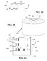
- FIGS. 1A , 1 B and 1 Care perspective views ( FIGS. 1A and 1B ) and a cross section ( FIG. 1C ) of a RRAM cell as exemplified;
- FIGS. 2A and 2Bare perspective views of a memory cell as exemplified
- FIG. 4is a cross sectional illustration of a memory device as exemplified herein;
- FIG. 6is a schematic illustration of an exemplary memory array as exemplified herein;
- FIGS. 7A through 7Jdepict an exemplary method of forming a device as disclosed herein.
- spatially related termsincluding but not limited to, “lower”, “upper”, “beneath”, “below”, “above”, and “on top”, if used herein, are utilized for ease of description to describe spatial relationships of an element(s) to another.
- Such spatially related termsencompass different orientations of the device in use or operation in addition to the particular orientations depicted in the figures and described herein. For example, if a cell depicted in the figures is turned over or flipped over, portions previously described as below or beneath other elements would then be above those other elements.
- an element, component or layer for examplewhen an element, component or layer for example is described as being “on” “connected to”, “coupled with” or “in contact with” another element, component or layer, it can be directly on, directly connected to, directly coupled with, in direct contact with, or intervening elements, components or layers may be on, connected, coupled or in contact with the particular element, component or layer, for example.
- an element, component or layer for exampleis referred to as begin “directly on”, “directly connected to”, “directly coupled with”, or “directly in contact with” another element, there are no intervening elements, components or layers for example.
- FIGS. 1A and 1BAn exemplary RRAM cell is illustrated in the perspective views of FIGS. 1A and 1B .
- the RRAM cell in FIGS. 1A and 1Bincludes a first electrode 110 , a resistive layer 120 and a second electrode 130 .
- the first electrode 110 , the resistive layer 120 and the second electrode 130generally have structures that nest inside one another, i.e. the second electrode 130 nests in the resistive layer 120 and the resistive layer 120 nests in the first electrode 110 .
- the particular structure or shape of the individual componentsis not generally limited in that their structures are related so that they are able to be nested structures.
- the RRAM cellcan be located or formed within, disposed on, or partially located or formed within a substrate.
- the second electrode 130could be a cuboid (or rectangular prism) having a particular relationship between the length, height and depth.
- the resistive layer 120could be a cuboid having the same particular relationship of length, height and depth but having an empty volume inside of the cuboid in which the second electrode 130 can be encompassed.
- the first electrode 110could be a cuboid having the same particular relationship of length, height and depth but having an empty volume inside of the cuboid in which the resistive layer 120 can be encompassed.
- FIG. 1Bdepicts another exemplary embodiment of a RRAM cell.
- the second electrode 130could be a right circular cylinder having a particular relationship between the height and radius.
- the resistive layer 120could be a right circular cylinder having the same particular relationship between height and radius but having an empty volume inside of the right circular cylinder in which the second electrode 130 can be encompassed.
- the first electrode 110could be a right circular cylinder having the same particular relationship between height and radius but having an empty volume inside of the right circular cylinder in which the resistive layer 120 can be encompassed.
- shapes other those depicted in FIGS. 1A and 1Bsuch as for example, elliptic cylinders, parabolic cylinders, hyperbolic cylinders, and cubes can be utilized in exemplary RRAM cells as disclosed herein.
- the exemplary RRAM cellalso includes a resistive layer 120 .
- the resistive layer 120has a lower portion 128 , a continuous side portion 121 and an upper portion 126 .
- the lower portion 128 and the continuous side portion 121have an outer surface 122 and an inner surface 124 .
- the resistive layer 120nests inside the first electrode 110 .
- the outer surface 122 of the resistive layer 120contacts the inner surface 114 of the first electrode 110 .
- the outer surface 122 of the resistive layer 120directly contacts the inner surface 114 of the first electrode 110 .
- the inner surface 124 of the resistive layer 120contacts the outer surface 132 of the second electrode 130 .
- the inner surface 124 of the resistive layer 120directly contacts the outer surface 132 of the second electrode 130 .
- the exemplary RRAM cellalso includes a second electrode 130 .
- the second electrode 130has a lower portion 138 and an upper portion 136 .
- the second electrode 130is generally not characterized as having a continuous side portion because it is a solid three dimensional shape as opposed to a hollow three dimensional shape as the first electrode 110 and the resistive layer 120 are.
- the second electrode 130nests inside the resistive layer 120 .
- the second electrode 120has an outer surface 132 .
- RRAM cells as disclosed hereingenerally afford a larger contact area between the electrodes and the resistive layer than do previously utilized RRAM cell structures.
- the size of the contact areais proportional to the strength of the signal of the RRAM cell and therefore can be indirectly proportional to the current required to read the cell.
- the contact area between the first electrode 210 and the resistive layer 220 in a RRAM cell as disclosed hereinis the contact area around all four sides of the RRAM cell. Therefore, the contact area equals 2(h ⁇ t 1 )(d ⁇ 2t 1 )+2(h ⁇ t 1 )(l ⁇ 2t 1 ).
- the second electrode contact area with the resistive layerwill be smaller than the first electrode (2(h ⁇ t 1 ⁇ t 2 )(d ⁇ 2t 1 ⁇ 2t 2 )+2(h ⁇ t 1 ⁇ t 2 )(l ⁇ 2t 1 ⁇ 2t 2 )), but will still be larger than in previously utilized RRAM cells.
- RRAM cells as disclosed hereincan offer larger contact areas without utilizing a larger area of a memory chip. Therefore, embodiments of RRAM cells as disclosed herein can afford larger areal densities while increasing the contact area of the electrodes and the resistive layer, which can afford enhanced functioning of the RRAM cell.
- FIGS. 3A and 3BOther exemplary embodiments of a RRAM cell are illustrated in FIGS. 3A and 3B .
- the RRAM cells depicted in FIGS. 3A and 3Binclude a semiconducting layer 325 .
- a semiconductor layer 325if utilized, can function to change the barrier height across the resistive layer 320 which can decrease the switching current.
- a semiconductor layer 325if utilized, can also function as a seed layer for the resistive layer 320 , which can provide an overlying layer having more desirable properties.
- a semiconductor layer 325if utilized, can function to change the barrier height across the resistive layer 320 and function as a seed layer for the resistive layer 320 .
- the semiconducting layer 325is located between the first electrode 310 and the resistive layer 320 .
- the semiconducting layer 325nests inside the first electrode 310 ; the resistive layer 320 nests inside the semiconducting layer 325 ; and the second electrode 330 nests inside the resistive layer 320 .
- the semiconducting layer 325similar to the other elements, includes a lower portion 348 , a continuous side portion 341 , and an upper portion 346 .
- the lower portion 348 and the continuous side portion 341form an inner surface 342 and an outer surface 344 .
- the outer surface 344 of the semiconducting layer 325contacts the inner surface 312 of the first electrode 310 . In an embodiment, the outer surface 344 of the semiconducting layer 325 directly contacts the inner surface 312 of the first electrode 310 . In an embodiment, the inner surface 342 of the semiconducting layer 325 contacts the outer surface 324 of the resistive layer 320 . In an embodiment, the inner surface 342 of the semiconducting layer 325 directly contacts the outer surface 324 of the resistive layer 320 .
- the first electrodecan be fabricated using commonly utilized materials and methods. In an embodiment, the first electrode can be fabricated using techniques that can achieve good conformal sidewall deposition. Exemplary techniques include, but are not limited to, plasma vapor deposition (PVD), ionized plasma based sputtering, long throw sputtering, chemical vapor deposition (CVD) and atomic layer deposition (ALD). In an embodiment, the first electrode can include oxidation resistant metal layers. In an embodiment, the first electrode can include iridium (Ir), platinum (Pt), titanium (Ti), ruthenium (Ru), tantalum (Ta), tungsten(W), copper (Cu), silver (Ag), aluminum (Al) or combinations thereof.
- the first electrodecan be Ir, Pt, IrO, TiN, TiAlN, Ru, RuO, W, Ta, Cu, Ag, Al, Ta, Pt, SrRuO 3 , RuO 2 , poly silicon, yttrium barium copper oxide (also referred to as “YBCO”, YBa 2 Cu 3 O 7 ), or lanthanum strontium copper oxide (also referred to as “LSCO”, La 2-x Sr x CuO 2 ).
- the first electrodecan generally be a substantially constant thickness layer that covers all surfaces of the volume in which it is located.
- the first electrodecan have a thickness (as given by t 1 in FIG. 2B ) of from about 50 nanometers (nm) to about 100 nm.
- the resistive layercan be fabricated using commonly utilized materials and methods.
- the resistive layercan be fabricated using techniques that can achieve good conformal sidewall deposition. Exemplary techniques include, but are not limited to, plasma vapor deposition (PVD), ionized plasma based sputtering, long throw sputtering, chemical vapor deposition (CVD) and atomic layer deposition (ALD).
- the resistive layercan include metal oxides, ferroelectric materials or combinations thereof.
- the resistive layerincludes a metal oxide material.
- the metal oxide materialcan be a binary oxide material or a complex metal oxide material.
- the metal oxide materialcan have components including, but not limited to aluminum (Al), titanium (Ti), tantalum (Ta), nickel (Ni), indium (In), zinc (Zn), chromium (Cr), hafnium (Hf), zirconium (Zr), iron (Fe), cobalt (Co), tin (Sn), niobium (Nb), strontium (Sr), manganese (Mn), copper (Cu) and combinations thereof
- Exemplary binary metal oxidesinclude, but are not limited to, CuO, NiO, CoO, ZnO, CrO 2 , TiO 2 , HfO 2 , ZrO 2 , Fe 2 O 3 , and Nb 2 O 5 .
- the resistive layerincludes one or more complex metal oxide materials, including, but not limited to, Pr 1-x Ca x MnO (where x ⁇ 1), La 1-x Sr x MnO 3 (where x ⁇ 1), SrFeO 2.7 , RuSr 2 GdCu 2 O 3 , YBa 2 Cu 3 O 7 , and combinations thereof.
- the resistive layerincludes one or more complex metal oxide materials, including, but not limited to, Pr 0.7 Ca 0.3 MnO 3 , La 0.7 Ca 0.3 MnO 3 and combinations thereof.
- the resistive layercan include one or more ferroelectric materials, including but not limited to, lead zirconate titanate (also referred to herein as “PZT”) having the formula PbZr x Ti 1-x O 3 where 0 ⁇ x ⁇ 1, lanthanum doped lead zirconate titanate (also referred to herein as “PLZT”, also called lead lanthanum zirconate titanate) having the formula Pb 0.83 La 0.17 (Zr 0.3 Ti 0.7 ) 0.9575 O 3 (PLZT 17/30/70), PtTiO 3 , SrTiO 3 , BaTiO 3 , BaSrTiO 3 , BaBiO, SrBi 4 Ti 4 O 15 , SrBi 2 Ta 2 O 9 , SrBi 2 TaNaO 3 (SBNT), Pb(Mg,Nb)O 3 , Pb 1.1 Nb 0.04 Zr 0.2 Ti 0.8 O 3 (PNZT), BaMgF 4
- the resistive layergenerally covers substantially all of the first electrode surface at a substantially constant thickness, and can have a thickness (as given by t 2 in FIG. 2B ) of from about 5 nanometers (nm) to about 100 nm. In an embodiment, it can have a thickness from about 5 nm to about 50 nm.
- the second electrodecan be fabricated using commonly utilized materials and methods.
- the second electrodecan be fabricated using techniques that can achieve good conformal sidewall deposition. Exemplary techniques include, but are not limited to, plasma vapor deposition (PVD), ionized plasma based sputtering, long throw sputtering, chemical vapor deposition (CVD) and atomic layer deposition (ALD).
- the second electrodecan include oxidation resistant metal layers.
- the second electrodecan include iridium (Ir), platinum (Pt), titanium (Ti), ruthenium (Ru), tantalum (Ta), tungsten (W), copper (Cu), silver (Ag), aluminum (Al) or combinations thereof.
- the second electrodecan be Ir, Pt, IrO, TiN, TiAlN, Ru, RuO, W, Ta, Cu, Ag, Al, Ta, Pt, SrRuO 3 , RuO 2 , poly silicon, yttrium barium copper oxide (also referred to as “YBCO”, YBa 2 Cu 3 O 7 ), or lanthanum strontium copper oxide (also referred to as “LSCO”, La 2-x Sr x CuO 2 ).
- Relevant dimensions of the second electrodecan depend at least in part on the shape of the RRAM cell, which is also the shape of the second electrode.
- the relevant dimensioncan be the radius or the diameter.
- the relevant dimensioncan be the length and depth of the second electrode.
- the diameter of the second electrodecan range from about 5 nm to about 30 nm.
- the length and depth of the second electrodecan both range from about 5 nm to about 30 nm. In embodiments where l 3 and d 3 are less than about 15 nm, the RRAM will most likely be cylinder, utilizing commonly known techniques.
- Exemplary embodiments of RRAM cells as disclosed hereincan include a semiconducting layer as discussed above.
- the semiconducting layercan be fabricated using commonly utilized materials and methods.
- the semiconducting layercan be fabricated using techniques that can achieve good conformal sidewall deposition. Exemplary techniques include, but are not limited to, plasma vapor deposition (PVD), ionized plasma based sputtering, long throw sputtering, chemical vapor deposition (CVD) and atomic layer deposition (ALD).
- PVDplasma vapor deposition
- CVDchemical vapor deposition
- ALDatomic layer deposition
- the semiconducting layercan include a semiconducting, non-ferroelectric material.
- the semiconducting, non-ferroelectric materialis a perovskite material.
- a perovskite materialis any material that has the same type of crystal structures as CaTiO 3 .
- Perovskitescan but need not be able to be represented by the general chemical formula of ABX 3 , where A and B are two cations of very different size, with A generally being larger than B, and X is an anion that bonds to both cations.
- a semiconducting non-ferroelectric materialis a niobium (Nb) doped strontium titanate (SrTiO also referred to as “STO”).
- Niobium (Nb) doped STOcan benefit from the good seed layer characteristics of STO and the semiconducting properties of the niobium (Nb) doping.
- Other exemplary semiconducting non-ferroelectric materialsinclude, but are not limited to chromium (Cr) doped STO and ruthenium (Ru) doped STO.
- the semiconducting layercan have a thickness of from about 50 nanometers (nm) to about 100 nm.
- FIG. 4illustrates a RRAM cell 401 that includes a top contact 455 and a bottom contact 440 .
- Elements that are included in FIG. 4 that are analogous to elements included in previous figures (such as FIG. 3C ) but are not discussed with respect to FIG. 4are numbered similarly.
- the top contact 455 and the bottom contact 440need not be present and the first electrode 410 and the second electrode 430 can electrically couple the RRAM cell 401 to another component(s).
- the top contact 455 and the bottom contact 440function to electrically couple or electrically contact the RRAM cell 401 to another component(s).
- the top contact 455 and the bottom contact 440can be made of any conductive material.
- the top contact 455can have a size that is similar to the size of the second electrode 430 so that the maximum contact area is achieved.
- an insulating layer 445can be utilized to electrically insulate the top contact 455 from other portions of the RRAM cell 401 , such as the first electrode 410 and the resistive layer 420 .
- the insulating layer 445covers the upper portions of the first electrode 410 and the resistive layer 420 .
- the top contactis disposed on the upper portion or top surface of the second electrode only; in such an embodiment, the insulating layer 445 can be disposed on the upper portion or top surfaces of the first electrode 410 and the resistive layer 420 .
- the bottom contact 440can electrically connect the RRAM cell 401 to a transistor 460 .
- the transistor 460may be any kind of transistors commonly utilized with RRAM cells, including but not limited to complimentary metal-oxide-semiconductor transistors (also referred to herein as “CMOS” transistors) such as p-type or n-type metal oxide semiconductor field effect transistors (also referred to herein as “MOSFET” transistors).
- CMOScomplimentary metal-oxide-semiconductor transistors
- MOSFETmetal oxide semiconductor field effect transistors
- the transistor 460may be formed in or on a substrate 450 .
- the RRAM cell 401may also be formed in, on, or partially in the same substrate 450 or a different substrate and later electrically coupled to the transistor 460 .
- FIG. 5illustrates a RRAM cell 501 electrically connected via a bottom contact 540 to a transistor 560 .
- the transistor 560includes a drain region 563 , a source region 565 and a gate region 561 .
- the source region 565can be electrically connected to a source line 566 ; and the top contact 555 can be electrically connected to a bit line 557 .
- the gate region 561can, but need not be connected to a word line.
- FIG. 6is a schematic circuit diagram of an illustrative memory array 601 .
- a plurality of memory devices 610(that each include a RRAM cell and a transistor for example) can be arranged in an array to form the memory array 601 .
- the memory array 601includes a number of parallel conductive bit lines 675 .
- the memory array 601also includes a number of parallel conductive word lines 670 that are generally orthogonal to the bit lines 675 .
- the word lines 670 and bit lines 675form a cross-point array where a memory device 610 can be disposed at each cross-point.
- RRAM cells as disclosed hereincan be fabricated using commonly utilized semiconductor fabrication techniques.
- An exemplary method of fabricating a RRAM cell as disclosed hereinis exemplified in FIGS. 7A through 7J .
- the steps depicted in FIGS. 7A to 7Jin no way limit the way in which a memory device as disclosed herein can be fabricated.
- the figuresare not necessarily to scale and do not necessarily depict the article at every state of preparation, i.e. intermediate stages of the article may not be illustrated in the sequence of figures.
- the materials and processes discussed with respect to FIGS. 7A to 7Jalso in no way limit materials or processes that can be utilized herein.
- FIG. 7Adepicts a substrate 750 .
- the substrate 750can include any substrate commonly utilized to fabricate memory devices. Exemplary substrates include, but are not limited to silicon, a mixture of silicon and germanium, and other similar materials.
- the substrate 750 depicted in FIG. 7Aincludes an already formed lower contact 740 .
- the lower contact 740can be formed of any conductive material. Exemplary conductive materials include, but are not limited to, Ag, Au, Pt, W and TiN.
- the lower contact 740(as well as other steps in this exemplary method) could have been formed using various etching and patterning techniques. Patterning generally describes a process or a series of processes that shape or alter the existing shape of the deposited materials and can be referred to as lithography.
- FIG. 7Bdepicts the article after the next step, deposition and exposure of a photoresist layer to form the photoresist mask 704 .
- a photoresist layerto form the photoresist mask 704 .
- Any commonly utilized type of photoresist material and photoresist processing techniquescan be utilized herein.
- the photoresist mask 704is utilized to etch a portion of the substrate 750 above the lower contact 740 , as seen in FIG. 7C . As seen in FIG. 7C the photoresist mask 704 protects a portion of the substrate while the portion that is gone allows etching of the substrate 750 to form a first void 708 .
- Commonly utilized etching techniquescan be utilized to etch the substrate 750 .
- FIG. 7Dillustrates the article after the photoresist mask 704 has been removed. Commonly utilized methods of processing and removing photoresist materials can be utilized herein. Removal of the photoresist mask 704 forms a second void 709 . The second void 709 will ultimately house the first electrode, the resistive layer and the second electrode of the RRAM cell.
- FIG. 7Eillustrates the article after a first conductive layer 714 has been deposited on at least a portion of the article.
- the first conductive layer 714can generally include materials as discussed above for the first electrode.
- the first conductive layer 714can be deposited using techniques including, but not limited to plasma vapor deposition (PVD), ionized plasma based sputtering, long throw sputtering, chemical vapor deposition (CVD) and atomic layer deposition (ALD).
- PVDplasma vapor deposition
- CVDchemical vapor deposition
- ALDatomic layer deposition
- Such techniquescan deposit a layer of conductive material that can conform to surfaces and sidewalls and produce a layer having substantially the same thickness across the layer.
- Deposition of the first conductive layer 714leaves a void, referred to herein as the third void 712 .
- the third void 712will ultimately house the resistive material and the second electrode of the RRAM cell.
- FIG. 7Fillustrates the article after a first oxide layer 716 has been deposited on at least a portion of the article.
- the first oxide layer 716can generally include materials as discussed above for the resistive layer.
- the first oxide layer 716can be deposited using techniques including, but not limited to plasma vapor deposition (PVD), ionized plasma based sputtering, long throw sputtering, chemical vapor deposition (CVD) and atomic layer deposition (ALD).
- PVDplasma vapor deposition
- CVDchemical vapor deposition
- ALDatomic layer deposition
- Such techniquescan deposit a layer of resistive material that can conform to surfaces and sidewalls and produce a layer having substantially the same thickness across the layer.
- Deposition of the first oxide layer 716leaves a void, referred to herein as the fourth void 718 .
- the fourth void 718will ultimately house the second electrode of the RRAM cell.
- FIG. 7Gillustrates the article after a second conductive layer 722 has been deposited on at least a portion of the article.
- the second conductive layer 722can generally include materials as discussed above for the second electrode.
- the second conductive layer 722can be deposited using techniques including, but not limited to plasma vapor deposition (PVD), ionized plasma based sputtering, long throw sputtering, chemical vapor deposition (CVD) and atomic layer deposition (ALD). Such techniques can deposit a layer of conductive material that can conform to surfaces and sidewalls. Deposition of the second conductive layer 722 generally substantially fills the fourth void 718 .
- the structure present on the substrate 750 at this point in this exemplary methodsubsumes the entire RRAM cell.
- FIG. 7Hillustrates the article after the next step, processing of the surface.
- This stepfunctions to make the top surfaces of the first electrode 710 , the resistive layer 720 and the second electrode 730 substantially coplanar with the portions of the substrate 750 surrounding the RRAM cell.
- An exemplary method of carrying out this processing stepincludes utilizing chemical-mechanical planarization (CMP).
- FIG. 7Iillustrates the article after an optional step, deposition of an insulating layer 724 .
- the insulating layergenerally covers at leas the top surfaces of the first electrode 710 and the resistive layer 720 and in the exemplary embodiment depicted in FIG. 7I covers those structures as well as at least a portion of the exposed substrate 750 .
- the insulating layer 724does not contact the second electrode 730 .
- the material making up the insulating layer 724can be deposited using known deposition methods, such as for example physical vapor deposition (PVD), chemical vapor deposition (CVD), electrochemical deposition (ECD), molecular beam epitaxy (MBE) and atomic layer deposition (ALD).
- PVDphysical vapor deposition
- CVDchemical vapor deposition
- ECDelectrochemical deposition
- MBEmolecular beam epitaxy
- ALDatomic layer deposition
- RRAM cells as disclosed hereincan be included in stand alone devices or can be integrated or embedded in devices that utilize the RAM, including but not limited to microprocessors (e.g., computer systems such as a PC e.g., a notebook computer or a desktop computer or a server) microcontrollers, dedicated machines such as cameras, and video or audio playback devices.
- microprocessorse.g., computer systems such as a PC e.g., a notebook computer or a desktop computer or a server
- dedicated machinessuch as cameras
- video or audio playback devicese.g., video or audio playback devices.
Landscapes
- Engineering & Computer Science (AREA)
- Chemical & Material Sciences (AREA)
- Materials Engineering (AREA)
- Manufacturing & Machinery (AREA)
- Semiconductor Memories (AREA)
Abstract
Description
Claims (20)
Priority Applications (2)
| Application Number | Priority Date | Filing Date | Title |
|---|---|---|---|
| US12/262,262US7791925B2 (en) | 2008-10-31 | 2008-10-31 | Structures for resistive random access memory cells |
| US12/835,791US8000128B2 (en) | 2008-10-31 | 2010-07-14 | Structures for resistive random access memory cells |
Applications Claiming Priority (1)
| Application Number | Priority Date | Filing Date | Title |
|---|---|---|---|
| US12/262,262US7791925B2 (en) | 2008-10-31 | 2008-10-31 | Structures for resistive random access memory cells |
Related Child Applications (1)
| Application Number | Title | Priority Date | Filing Date |
|---|---|---|---|
| US12/835,791ContinuationUS8000128B2 (en) | 2008-10-31 | 2010-07-14 | Structures for resistive random access memory cells |
Publications (2)
| Publication Number | Publication Date |
|---|---|
| US20100110758A1 US20100110758A1 (en) | 2010-05-06 |
| US7791925B2true US7791925B2 (en) | 2010-09-07 |
Family
ID=42131185
Family Applications (2)
| Application Number | Title | Priority Date | Filing Date |
|---|---|---|---|
| US12/262,262Active2029-02-05US7791925B2 (en) | 2008-10-31 | 2008-10-31 | Structures for resistive random access memory cells |
| US12/835,791Expired - Fee RelatedUS8000128B2 (en) | 2008-10-31 | 2010-07-14 | Structures for resistive random access memory cells |
Family Applications After (1)
| Application Number | Title | Priority Date | Filing Date |
|---|---|---|---|
| US12/835,791Expired - Fee RelatedUS8000128B2 (en) | 2008-10-31 | 2010-07-14 | Structures for resistive random access memory cells |
Country Status (1)
| Country | Link |
|---|---|
| US (2) | US7791925B2 (en) |
Cited By (5)
| Publication number | Priority date | Publication date | Assignee | Title |
|---|---|---|---|---|
| US8598562B2 (en) | 2011-07-01 | 2013-12-03 | Micron Technology, Inc. | Memory cell structures |
| US20210036057A1 (en)* | 2019-07-29 | 2021-02-04 | Taiwan Semiconductor Manufacturing Co., Ltd. | 3d rram cell structure for reducing forming and set voltages |
| US11056648B1 (en)* | 2019-12-12 | 2021-07-06 | SK Hynix Inc. | Semiconductor device including variable resistance element |
| US11227997B1 (en) | 2020-07-07 | 2022-01-18 | International Business Machines Corporation | Planar resistive random-access memory (RRAM) device with a shared top electrode |
| US11778932B2 (en) | 2019-11-22 | 2023-10-03 | Winbond Electronics Corp. | Resistive random access memory and manufacturing method thereof |
Families Citing this family (104)
| Publication number | Priority date | Publication date | Assignee | Title |
|---|---|---|---|---|
| US20130082232A1 (en) | 2011-09-30 | 2013-04-04 | Unity Semiconductor Corporation | Multi Layered Conductive Metal Oxide Structures And Methods For Facilitating Enhanced Performance Characteristics Of Two Terminal Memory Cells |
| US8022547B2 (en) | 2008-11-18 | 2011-09-20 | Seagate Technology Llc | Non-volatile memory cells including small volume electrical contact regions |
| KR20100062570A (en)* | 2008-12-02 | 2010-06-10 | 삼성전자주식회사 | Resistive random access memory |
| KR101556929B1 (en)* | 2009-03-23 | 2015-10-02 | 삼성전자주식회사 | Diode structure and resistive memory device including the same |
| KR101070291B1 (en)* | 2009-12-18 | 2011-10-06 | 주식회사 하이닉스반도체 | Resistive memory device and method for manufacturing the same |
| US9601692B1 (en) | 2010-07-13 | 2017-03-21 | Crossbar, Inc. | Hetero-switching layer in a RRAM device and method |
| US9570678B1 (en) | 2010-06-08 | 2017-02-14 | Crossbar, Inc. | Resistive RAM with preferental filament formation region and methods |
| US8946046B1 (en) | 2012-05-02 | 2015-02-03 | Crossbar, Inc. | Guided path for forming a conductive filament in RRAM |
| US8274812B2 (en) | 2010-06-14 | 2012-09-25 | Crossbar, Inc. | Write and erase scheme for resistive memory device |
| US9437297B2 (en) | 2010-06-14 | 2016-09-06 | Crossbar, Inc. | Write and erase scheme for resistive memory device |
| US20120007035A1 (en)* | 2010-07-12 | 2012-01-12 | Crossbar, Inc. | Intrinsic Programming Current Control for a RRAM |
| US8884261B2 (en) | 2010-08-23 | 2014-11-11 | Crossbar, Inc. | Device switching using layered device structure |
| US8569172B1 (en) | 2012-08-14 | 2013-10-29 | Crossbar, Inc. | Noble metal/non-noble metal electrode for RRAM applications |
| USRE46335E1 (en) | 2010-11-04 | 2017-03-07 | Crossbar, Inc. | Switching device having a non-linear element |
| US8502185B2 (en) | 2011-05-31 | 2013-08-06 | Crossbar, Inc. | Switching device having a non-linear element |
| KR101069124B1 (en) | 2010-11-05 | 2011-10-05 | 재단법인대구경북과학기술원 | Nonvolatile Resistance Change Memory Device |
| KR101215951B1 (en)* | 2011-03-24 | 2013-01-21 | 에스케이하이닉스 주식회사 | Semiconductor Memory And Manufacturing Method Thereof |
| US8519375B2 (en) | 2011-04-19 | 2013-08-27 | Winbond Electronics Corp. | Non-volatile memory with oxygen vacancy barrier layer |
| US9620206B2 (en) | 2011-05-31 | 2017-04-11 | Crossbar, Inc. | Memory array architecture with two-terminal memory cells |
| US8619459B1 (en) | 2011-06-23 | 2013-12-31 | Crossbar, Inc. | High operating speed resistive random access memory |
| US8659929B2 (en) | 2011-06-30 | 2014-02-25 | Crossbar, Inc. | Amorphous silicon RRAM with non-linear device and operation |
| US9627443B2 (en) | 2011-06-30 | 2017-04-18 | Crossbar, Inc. | Three-dimensional oblique two-terminal memory with enhanced electric field |
| US8946669B1 (en) | 2012-04-05 | 2015-02-03 | Crossbar, Inc. | Resistive memory device and fabrication methods |
| US9166163B2 (en) | 2011-06-30 | 2015-10-20 | Crossbar, Inc. | Sub-oxide interface layer for two-terminal memory |
| US9564587B1 (en) | 2011-06-30 | 2017-02-07 | Crossbar, Inc. | Three-dimensional two-terminal memory with enhanced electric field and segmented interconnects |
| US9058865B1 (en) | 2011-06-30 | 2015-06-16 | Crossbar, Inc. | Multi-level cell operation in silver/amorphous silicon RRAM |
| US8846484B2 (en)* | 2012-02-15 | 2014-09-30 | Intermolecular, Inc. | ReRAM stacks preparation by using single ALD or PVD chamber |
| US8971088B1 (en) | 2012-03-22 | 2015-03-03 | Crossbar, Inc. | Multi-level cell operation using zinc oxide switching material in non-volatile memory device |
| US9685608B2 (en) | 2012-04-13 | 2017-06-20 | Crossbar, Inc. | Reduced diffusion in metal electrode for two-terminal memory |
| US8658476B1 (en)* | 2012-04-20 | 2014-02-25 | Crossbar, Inc. | Low temperature P+ polycrystalline silicon material for non-volatile memory device |
| US9053781B2 (en) | 2012-06-15 | 2015-06-09 | Taiwan Semiconductor Manufacturing Company, Ltd. | Structure and method for a forming free resistive random access memory with multi-level cell |
| US9680091B2 (en) | 2012-06-15 | 2017-06-13 | Taiwan Semiconductor Manufacturing Company, Ltd. | Structure and method for a complimentary resistive switching random access memory for high density application |
| US9583556B2 (en) | 2012-07-19 | 2017-02-28 | Taiwan Semiconductor Manufacturing Company, Ltd. | Process-compatible decoupling capacitor and method for making the same |
| US8896096B2 (en) | 2012-07-19 | 2014-11-25 | Taiwan Semiconductor Manufacturing Company, Ltd. | Process-compatible decoupling capacitor and method for making the same |
| US9583701B1 (en) | 2012-08-14 | 2017-02-28 | Crossbar, Inc. | Methods for fabricating resistive memory device switching material using ion implantation |
| US9741765B1 (en) | 2012-08-14 | 2017-08-22 | Crossbar, Inc. | Monolithically integrated resistive memory using integrated-circuit foundry compatible processes |
| US9847480B2 (en) | 2012-09-28 | 2017-12-19 | Taiwan Semiconductor Manufacturing Company, Ltd. | Resistance variable memory structure and method of forming the same |
| US9576616B2 (en) | 2012-10-10 | 2017-02-21 | Crossbar, Inc. | Non-volatile memory with overwrite capability and low write amplification |
| US8921818B2 (en) | 2012-11-09 | 2014-12-30 | Taiwan Semiconductor Manufacturing Company, Ltd. | Resistance variable memory structure |
| US9231197B2 (en)* | 2012-11-12 | 2016-01-05 | Taiwan Semiconductor Manufacturing Company, Ltd. | Logic compatible RRAM structure and process |
| US8742390B1 (en) | 2012-11-12 | 2014-06-03 | Taiwan Semiconductor Manufacturing Company, Ltd. | Logic compatible RRAM structure and process |
| US9019743B2 (en) | 2012-11-29 | 2015-04-28 | Taiwan Semiconductor Manufacturing Company, Ltd. | Method and structure for resistive switching random access memory with high reliable and high density |
| US9431604B2 (en) | 2012-12-14 | 2016-08-30 | Taiwan Semiconductor Manufacturing Company, Ltd. | Resistive random access memory (RRAM) and method of making |
| US9023699B2 (en) | 2012-12-20 | 2015-05-05 | Taiwan Semiconductor Manufacturing Company, Ltd. | Resistive random access memory (RRAM) structure and method of making the RRAM structure |
| US9130162B2 (en) | 2012-12-20 | 2015-09-08 | Taiwan Semiconductor Manufacturing Company, Ltd. | Resistance variable memory structure and method of forming the same |
| US9331277B2 (en) | 2013-01-21 | 2016-05-03 | Taiwan Semiconductor Manufacturing Company, Ltd. | One transistor and one resistive random access memory (RRAM) structure with spacer |
| US8908415B2 (en) | 2013-03-01 | 2014-12-09 | Taiwan Semiconductor Manufacturing Company, Ltd. | Resistive memory reset |
| US8963114B2 (en) | 2013-03-06 | 2015-02-24 | Taiwan Semiconductor Manufacturing Company, Ltd. | One transistor and one resistive (1T1R) random access memory (RRAM) structure with dual spacers |
| US9424917B2 (en) | 2013-03-07 | 2016-08-23 | Taiwan Semiconductor Manufacturing Company, Ltd. | Method for operating RRAM memory |
| US8952347B2 (en) | 2013-03-08 | 2015-02-10 | Taiwan Semiconductor Manfacturing Company, Ltd. | Resistive memory cell array with top electrode bit line |
| US9478638B2 (en) | 2013-03-12 | 2016-10-25 | Taiwan Semiconductor Manufacturing Company, Ltd. | Resistive switching random access memory with asymmetric source and drain |
| US9231205B2 (en) | 2013-03-13 | 2016-01-05 | Taiwan Semiconductor Manufacturing Company, Ltd. | Low form voltage resistive random access memory (RRAM) |
| US9093635B2 (en) | 2013-03-14 | 2015-07-28 | Crossbar, Inc. | Controlling on-state current for two-terminal memory |
| US9153624B2 (en) | 2013-03-14 | 2015-10-06 | Crossbar, Inc. | Scaling of filament based RRAM |
| US9349953B2 (en) | 2013-03-15 | 2016-05-24 | Taiwan Semiconductor Manufacturing Company, Ltd. | Resistance variable memory structure and method of forming the same |
| CN103236497B (en)* | 2013-04-25 | 2015-10-28 | 桂林电子科技大学 | A kind of resistance-variable storing device based on bismuth titanates and preparation method thereof |
| CN104300081B (en)* | 2013-07-15 | 2017-05-03 | 中国科学院苏州纳米技术与纳米仿生研究所 | Heating electrode of phase change memory and manufacturing method thereof |
| US9337210B2 (en) | 2013-08-12 | 2016-05-10 | Micron Technology, Inc. | Vertical ferroelectric field effect transistor constructions, constructions comprising a pair of vertical ferroelectric field effect transistors, vertical strings of ferroelectric field effect transistors, and vertical strings of laterally opposing pairs of vertical ferroelectric field effect transistors |
| US9299927B2 (en) | 2013-08-16 | 2016-03-29 | Taiwan Semiconductor Manufacturing Company, Ltd. | Memory cell having resistance variable film and method of making the same |
| US9837605B2 (en) | 2013-08-16 | 2017-12-05 | Taiwan Semiconductor Manufacturing Company, Ltd. | Memory cell having resistance variable film and method of making the same |
| US9112148B2 (en)* | 2013-09-30 | 2015-08-18 | Taiwan Semiconductor Manufacturing Co., Ltd. | RRAM cell structure with laterally offset BEVA/TEVA |
| US9076522B2 (en) | 2013-09-30 | 2015-07-07 | Taiwan Semiconductor Manufacturing Co., Ltd. | Memory cells breakdown protection |
| US9286974B2 (en) | 2013-10-23 | 2016-03-15 | Taiwan Semiconductor Manufacturing Co., Ltd. | Memory devices |
| US8981334B1 (en) | 2013-11-01 | 2015-03-17 | Micron Technology, Inc. | Memory cells having regions containing one or both of carbon and boron |
| US9172036B2 (en) | 2013-11-22 | 2015-10-27 | Taiwan Semiconductor Manufacturing Co., Ltd. | Top electrode blocking layer for RRAM device |
| US9385316B2 (en) | 2014-01-07 | 2016-07-05 | Taiwan Semiconductor Manufacturing Co., Ltd. | RRAM retention by depositing Ti capping layer before HK HfO |
| US10290801B2 (en) | 2014-02-07 | 2019-05-14 | Crossbar, Inc. | Scalable silicon based resistive memory device |
| US10003022B2 (en) | 2014-03-04 | 2018-06-19 | Taiwan Semiconductor Manufacturing Co., Ltd. | RRAM cell structure with conductive etch-stop layer |
| KR102087744B1 (en)* | 2014-03-17 | 2020-03-11 | 에스케이하이닉스 주식회사 | Electronic device and method for fabricating the same |
| SG11201606383YA (en)* | 2014-03-25 | 2016-09-29 | Intel Corporaton | Techniques for forming non-planar resistive memory cells |
| US9178144B1 (en) | 2014-04-14 | 2015-11-03 | Taiwan Semiconductor Manufacturing Co., Ltd. | RRAM cell with bottom electrode |
| US9263577B2 (en) | 2014-04-24 | 2016-02-16 | Micron Technology, Inc. | Ferroelectric field effect transistors, pluralities of ferroelectric field effect transistors arrayed in row lines and column lines, and methods of forming a plurality of ferroelectric field effect transistors |
| US9472560B2 (en)* | 2014-06-16 | 2016-10-18 | Micron Technology, Inc. | Memory cell and an array of memory cells |
| US10611161B2 (en) | 2014-07-24 | 2020-04-07 | Avision Inc. | Image forming agent storage member and laser printer using the same |
| US9224470B1 (en) | 2014-08-05 | 2015-12-29 | Taiwan Semiconductor Manufacturing Company, Ltd. | Memory circuit and method of programming memory circuit |
| US9159829B1 (en) | 2014-10-07 | 2015-10-13 | Micron Technology, Inc. | Recessed transistors containing ferroelectric material |
| US9209392B1 (en) | 2014-10-14 | 2015-12-08 | Taiwan Semiconductor Manufacturing Co., Ltd. | RRAM cell with bottom electrode |
| US9276092B1 (en) | 2014-10-16 | 2016-03-01 | Micron Technology, Inc. | Transistors and methods of forming transistors |
| EP3234998A4 (en) | 2014-12-18 | 2018-08-15 | Intel Corporation | Resistive memory cells including localized filamentary channels, devices including the same, and methods of making the same |
| US20160181517A1 (en)* | 2014-12-23 | 2016-06-23 | Silicon Storage Technology, Inc. | Geometrically Enhanced Resistive Random Access Memory (RRAM) Cell And Method Of Forming Same |
| CN107004761B (en) | 2014-12-24 | 2021-09-14 | 英特尔公司 | Resistive memory cells and precursors thereof, methods of making the same, and devices including the same |
| FR3031416B1 (en) | 2015-01-06 | 2018-09-07 | Commissariat Energie Atomique | RESISTIVE NON-VOLATILE MEMORY CELL AND METHOD OF MANUFACTURING THE SAME |
| TWI559519B (en) | 2015-02-16 | 2016-11-21 | 國立清華大學 | Resistive memory |
| US9305929B1 (en) | 2015-02-17 | 2016-04-05 | Micron Technology, Inc. | Memory cells |
| US10134982B2 (en) | 2015-07-24 | 2018-11-20 | Micron Technology, Inc. | Array of cross point memory cells |
| US9853211B2 (en) | 2015-07-24 | 2017-12-26 | Micron Technology, Inc. | Array of cross point memory cells individually comprising a select device and a programmable device |
| US9768231B2 (en)* | 2016-02-12 | 2017-09-19 | Globalfoundries Singapore Pte. Ltd. | High density multi-time programmable resistive memory devices and method of forming thereof |
| US9859338B2 (en)* | 2016-03-21 | 2018-01-02 | Winbond Electronics Corp. | Three-dimensional resistive memory |
| US10396145B2 (en) | 2017-01-12 | 2019-08-27 | Micron Technology, Inc. | Memory cells comprising ferroelectric material and including current leakage paths having different total resistances |
| US10319426B2 (en)* | 2017-05-09 | 2019-06-11 | Micron Technology, Inc. | Semiconductor structures, memory cells and devices comprising ferroelectric materials, systems including same, and related methods |
| EP3688805A4 (en)* | 2017-09-29 | 2021-04-14 | INTEL Corporation | VERTICAL REAR SIDE TRANSISTOR WITH FERROELECTRIC MATERIAL |
| US10608179B2 (en)* | 2017-11-30 | 2020-03-31 | International Business Machines Corporation | Resistive random access memory with metal fin electrode |
| CN108054277A (en)* | 2017-12-25 | 2018-05-18 | 扬州大学 | BaTiO3The preparation method of base superelevation on-off ratio resistive device |
| US11888034B2 (en) | 2019-06-07 | 2024-01-30 | Intel Corporation | Transistors with metal chalcogenide channel materials |
| US11171243B2 (en) | 2019-06-27 | 2021-11-09 | Intel Corporation | Transistor structures with a metal oxide contact buffer |
| US11777029B2 (en) | 2019-06-27 | 2023-10-03 | Intel Corporation | Vertical transistors for ultra-dense logic and memory applications |
| CN111092147B (en)* | 2019-07-05 | 2022-02-08 | 河南大学 | PBCO/NSTO superconducting resistive random access memory and preparation method thereof |
| US11170834B2 (en) | 2019-07-10 | 2021-11-09 | Micron Technology, Inc. | Memory cells and methods of forming a capacitor including current leakage paths having different total resistances |
| KR102840448B1 (en) | 2019-12-18 | 2025-07-29 | 삼성전자주식회사 | Nonvolatile memory cell and nonvolatile memory device comprising the same |
| CN114078901A (en) | 2020-08-19 | 2022-02-22 | 联华电子股份有限公司 | Resistive memory device and manufacturing method thereof |
| US12266720B2 (en) | 2020-12-21 | 2025-04-01 | Intel Corporation | Transistors with monocrystalline metal chalcogenide channel materials |
| CN114361336B (en)* | 2021-12-29 | 2023-02-14 | 华中科技大学 | SrFeOx resistive memory with multi-valued properties, its preparation and application |
| CN117042466A (en)* | 2022-04-28 | 2023-11-10 | 联华电子股份有限公司 | Resistive memory structure and manufacturing method thereof |
| TW202517129A (en)* | 2023-10-03 | 2025-04-16 | 聯華電子股份有限公司 | Semiconductor device and manufacturing method thereof |
Citations (5)
| Publication number | Priority date | Publication date | Assignee | Title |
|---|---|---|---|---|
| US6104632A (en)* | 1998-05-18 | 2000-08-15 | Canon Kabushiki Kaisha | Magnetic thin film memory and recording and reproducing method and apparatus using such a memory |
| US6111784A (en)* | 1997-09-18 | 2000-08-29 | Canon Kabushiki Kaisha | Magnetic thin film memory element utilizing GMR effect, and recording/reproduction method using such memory element |
| US20080089104A1 (en)* | 2006-09-28 | 2008-04-17 | Hiroyasu Tanaka | Semiconductor memory device and method for fabricating semiconductor memory device |
| US20080304311A1 (en)* | 2007-06-07 | 2008-12-11 | Jan Boris Philipp | Integrated circuit including logic portion and memory portion |
| US7608848B2 (en)* | 2006-05-09 | 2009-10-27 | Macronix International Co., Ltd. | Bridge resistance random access memory device with a singular contact structure |
Family Cites Families (1)
| Publication number | Priority date | Publication date | Assignee | Title |
|---|---|---|---|---|
| JP4509467B2 (en)* | 2002-11-08 | 2010-07-21 | シャープ株式会社 | Nonvolatile variable resistance element and storage device |
- 2008
- 2008-10-31USUS12/262,262patent/US7791925B2/enactiveActive
- 2010
- 2010-07-14USUS12/835,791patent/US8000128B2/ennot_activeExpired - Fee Related
Patent Citations (5)
| Publication number | Priority date | Publication date | Assignee | Title |
|---|---|---|---|---|
| US6111784A (en)* | 1997-09-18 | 2000-08-29 | Canon Kabushiki Kaisha | Magnetic thin film memory element utilizing GMR effect, and recording/reproduction method using such memory element |
| US6104632A (en)* | 1998-05-18 | 2000-08-15 | Canon Kabushiki Kaisha | Magnetic thin film memory and recording and reproducing method and apparatus using such a memory |
| US7608848B2 (en)* | 2006-05-09 | 2009-10-27 | Macronix International Co., Ltd. | Bridge resistance random access memory device with a singular contact structure |
| US20080089104A1 (en)* | 2006-09-28 | 2008-04-17 | Hiroyasu Tanaka | Semiconductor memory device and method for fabricating semiconductor memory device |
| US20080304311A1 (en)* | 2007-06-07 | 2008-12-11 | Jan Boris Philipp | Integrated circuit including logic portion and memory portion |
Non-Patent Citations (3)
| Title |
|---|
| H. Kohlstedt et al., Physical Rev. B (72) 125431( 2005). |
| J.C. Bruyere et al., Appl. Phys. Letters (16) 40 (1970). |
| Kohtaroch Gotoh et al., Jpn. J. Appl. Phys. (25) 39 (1996). |
Cited By (14)
| Publication number | Priority date | Publication date | Assignee | Title |
|---|---|---|---|---|
| US8598562B2 (en) | 2011-07-01 | 2013-12-03 | Micron Technology, Inc. | Memory cell structures |
| US9070874B2 (en) | 2011-07-01 | 2015-06-30 | Micron Technology, Inc. | Memory cell structures |
| US9385315B2 (en) | 2011-07-01 | 2016-07-05 | Micron Technology, Inc. | Memory cell structures |
| US9755144B2 (en) | 2011-07-01 | 2017-09-05 | Micron Technology, Inc. | Memory cell structures |
| US10608178B2 (en) | 2011-07-01 | 2020-03-31 | Micron Technology, Inc. | Memory cell structures |
| TWI730786B (en)* | 2019-07-29 | 2021-06-11 | 台灣積體電路製造股份有限公司 | Integrated circuit device and manufacturing method thereof |
| US20210036057A1 (en)* | 2019-07-29 | 2021-02-04 | Taiwan Semiconductor Manufacturing Co., Ltd. | 3d rram cell structure for reducing forming and set voltages |
| US11088203B2 (en)* | 2019-07-29 | 2021-08-10 | Taiwan Semiconductor Manufacturing Company, Ltd. | 3D RRAM cell structure for reducing forming and set voltages |
| US11751406B2 (en) | 2019-07-29 | 2023-09-05 | Taiwan Semiconductor Manufacturing Company, Ltd. | 3D RRAM cell structure for reducing forming and set voltages |
| US11778932B2 (en) | 2019-11-22 | 2023-10-03 | Winbond Electronics Corp. | Resistive random access memory and manufacturing method thereof |
| US12193344B2 (en) | 2019-11-22 | 2025-01-07 | Winbond Electronics Corp | Method for manufacturing resistive random access memory |
| US11056648B1 (en)* | 2019-12-12 | 2021-07-06 | SK Hynix Inc. | Semiconductor device including variable resistance element |
| US11380844B2 (en) | 2019-12-12 | 2022-07-05 | SK Hynix Inc. | Semiconductor device including variable resistance element |
| US11227997B1 (en) | 2020-07-07 | 2022-01-18 | International Business Machines Corporation | Planar resistive random-access memory (RRAM) device with a shared top electrode |
Also Published As
| Publication number | Publication date |
|---|---|
| US20100110758A1 (en) | 2010-05-06 |
| US20100277969A1 (en) | 2010-11-04 |
| US8000128B2 (en) | 2011-08-16 |
Similar Documents
| Publication | Publication Date | Title |
|---|---|---|
| US7791925B2 (en) | Structures for resistive random access memory cells | |
| US10676722B2 (en) | Arrays of memory cells individually comprising a capacitor and an elevationally-extending transistor, methods of forming a tier of an array of memory cells, and methods of forming an array of memory cells individually comprising a capacitor and an elevationally-extending transistor | |
| US11508741B2 (en) | Nonvolatile memory device having resistance change structure | |
| US7961496B2 (en) | Resistive memory cells and devices having asymmetrical contacts | |
| US7535035B2 (en) | Cross-point nonvolatile memory devices using binary metal oxide layer as data storage material layer and methods of fabricating the same | |
| US8546861B2 (en) | Resistance change memory device with three-dimensional structure, and device array, electronic product and manufacturing method therefor | |
| US7439082B2 (en) | Conductive memory stack with non-uniform width | |
| US20040228172A1 (en) | Conductive memory stack with sidewall | |
| US20080048226A1 (en) | Direct cell via structures for ferroelectric random access memory devices and methods of fabricating such structures | |
| JP2006060209A (en) | Semiconductive metal oxide thin film ferroelectric memory transistor | |
| KR20080096432A (en) | Nonvolatile Semiconductor Memory and Manufacturing Method Thereof | |
| US8518792B2 (en) | Method for fabricating a damascene self-aligned ferroelectric random access memory (F-RAM) having a ferroelectric capacitor aligned with a three dimensional transistor structure | |
| CN101432879A (en) | Variable resistance element and manufacturing method thereof | |
| US20090130457A1 (en) | Dielectric structure | |
| US9825099B2 (en) | Switching element, switching element array, and resistive random access memory including switching element, and methods of manufacturing the same | |
| US9666798B1 (en) | Switching elements, resistive random access memory devices including the same, and methods of manufacturing the switching elements and the resistive random access memory devices | |
| US11289157B1 (en) | Memory device | |
| US8552515B2 (en) | Method for fabricating a damascene self-aligned ferroelectric random access memory (F-RAM) device structure employing reduced processing steps | |
| US8518791B2 (en) | Method for fabricating a damascene self-aligned ferroelectric random access memory (F-RAM) with simultaneous formation of sidewall ferroelectric capacitors | |
| KR100993052B1 (en) | A resistive change memory device, a resistive change memory device array, an electronic product, and a manufacturing method of the device having a three-dimensional structure | |
| US20170338409A1 (en) | Switching element, resistive memory device including switching element, and methods of manufacturing the same | |
| US20100096611A1 (en) | Vertically integrated memory structures | |
| US20140021432A1 (en) | Variable resistance memory device and method for fabricating the same | |
| KR20100116826A (en) | Resistance change memory device array including selection device and 3-dimensional resistance change memory device, electronic product, and method for fabricating the device array | |
| KR100998256B1 (en) | Vertical nonvolatile memory device and manufacturing method thereof |
Legal Events
| Date | Code | Title | Description |
|---|---|---|---|
| AS | Assignment | Owner name:SEAGATE TECHNOLOGY LLC,CALIFORNIA Free format text:ASSIGNMENT OF ASSIGNORS INTEREST;ASSIGNORS:LI, SHAOPING;JIN, INSIK;GAO, ZHENG;AND OTHERS;SIGNING DATES FROM 20081029 TO 20081030;REEL/FRAME:021768/0759 Owner name:SEAGATE TECHNOLOGY LLC, CALIFORNIA Free format text:ASSIGNMENT OF ASSIGNORS INTEREST;ASSIGNORS:LI, SHAOPING;JIN, INSIK;GAO, ZHENG;AND OTHERS;SIGNING DATES FROM 20081029 TO 20081030;REEL/FRAME:021768/0759 | |
| AS | Assignment | Owner name:WELLS FARGO BANK, NATIONAL ASSOCIATION, AS COLLATERAL AGENT AND SECOND PRIORITY REPRESENTATIVE, CALIFORNIA Free format text:SECURITY AGREEMENT;ASSIGNORS:MAXTOR CORPORATION;SEAGATE TECHNOLOGY LLC;SEAGATE TECHNOLOGY INTERNATIONAL;REEL/FRAME:022757/0017 Effective date:20090507 Owner name:JPMORGAN CHASE BANK, N.A., AS ADMINISTRATIVE AGENT AND FIRST PRIORITY REPRESENTATIVE, NEW YORK Free format text:SECURITY AGREEMENT;ASSIGNORS:MAXTOR CORPORATION;SEAGATE TECHNOLOGY LLC;SEAGATE TECHNOLOGY INTERNATIONAL;REEL/FRAME:022757/0017 Effective date:20090507 Owner name:JPMORGAN CHASE BANK, N.A., AS ADMINISTRATIVE AGENT Free format text:SECURITY AGREEMENT;ASSIGNORS:MAXTOR CORPORATION;SEAGATE TECHNOLOGY LLC;SEAGATE TECHNOLOGY INTERNATIONAL;REEL/FRAME:022757/0017 Effective date:20090507 Owner name:WELLS FARGO BANK, NATIONAL ASSOCIATION, AS COLLATE Free format text:SECURITY AGREEMENT;ASSIGNORS:MAXTOR CORPORATION;SEAGATE TECHNOLOGY LLC;SEAGATE TECHNOLOGY INTERNATIONAL;REEL/FRAME:022757/0017 Effective date:20090507 | |
| FEPP | Fee payment procedure | Free format text:PAYER NUMBER DE-ASSIGNED (ORIGINAL EVENT CODE: RMPN); ENTITY STATUS OF PATENT OWNER: LARGE ENTITY Free format text:PAYOR NUMBER ASSIGNED (ORIGINAL EVENT CODE: ASPN); ENTITY STATUS OF PATENT OWNER: LARGE ENTITY | |
| FEPP | Fee payment procedure | Free format text:PAYOR NUMBER ASSIGNED (ORIGINAL EVENT CODE: ASPN); ENTITY STATUS OF PATENT OWNER: LARGE ENTITY | |
| STCF | Information on status: patent grant | Free format text:PATENTED CASE | |
| AS | Assignment | Owner name:SEAGATE TECHNOLOGY LLC, CALIFORNIA Free format text:RELEASE;ASSIGNOR:JPMORGAN CHASE BANK, N.A., AS ADMINISTRATIVE AGENT;REEL/FRAME:025662/0001 Effective date:20110114 Owner name:MAXTOR CORPORATION, CALIFORNIA Free format text:RELEASE;ASSIGNOR:JPMORGAN CHASE BANK, N.A., AS ADMINISTRATIVE AGENT;REEL/FRAME:025662/0001 Effective date:20110114 Owner name:SEAGATE TECHNOLOGY INTERNATIONAL, CALIFORNIA Free format text:RELEASE;ASSIGNOR:JPMORGAN CHASE BANK, N.A., AS ADMINISTRATIVE AGENT;REEL/FRAME:025662/0001 Effective date:20110114 Owner name:SEAGATE TECHNOLOGY HDD HOLDINGS, CALIFORNIA Free format text:RELEASE;ASSIGNOR:JPMORGAN CHASE BANK, N.A., AS ADMINISTRATIVE AGENT;REEL/FRAME:025662/0001 Effective date:20110114 | |
| AS | Assignment | Owner name:THE BANK OF NOVA SCOTIA, AS ADMINISTRATIVE AGENT, CANADA Free format text:SECURITY AGREEMENT;ASSIGNOR:SEAGATE TECHNOLOGY LLC;REEL/FRAME:026010/0350 Effective date:20110118 Owner name:THE BANK OF NOVA SCOTIA, AS ADMINISTRATIVE AGENT, Free format text:SECURITY AGREEMENT;ASSIGNOR:SEAGATE TECHNOLOGY LLC;REEL/FRAME:026010/0350 Effective date:20110118 | |
| AS | Assignment | Owner name:SEAGATE TECHNOLOGY INTERNATIONAL, CAYMAN ISLANDS Free format text:TERMINATION AND RELEASE OF SECURITY INTEREST IN PATENT RIGHTS;ASSIGNOR:WELLS FARGO BANK, NATIONAL ASSOCIATION, AS COLLATERAL AGENT AND SECOND PRIORITY REPRESENTATIVE;REEL/FRAME:030833/0001 Effective date:20130312 Owner name:SEAGATE TECHNOLOGY US HOLDINGS, INC., CALIFORNIA Free format text:TERMINATION AND RELEASE OF SECURITY INTEREST IN PATENT RIGHTS;ASSIGNOR:WELLS FARGO BANK, NATIONAL ASSOCIATION, AS COLLATERAL AGENT AND SECOND PRIORITY REPRESENTATIVE;REEL/FRAME:030833/0001 Effective date:20130312 Owner name:SEAGATE TECHNOLOGY LLC, CALIFORNIA Free format text:TERMINATION AND RELEASE OF SECURITY INTEREST IN PATENT RIGHTS;ASSIGNOR:WELLS FARGO BANK, NATIONAL ASSOCIATION, AS COLLATERAL AGENT AND SECOND PRIORITY REPRESENTATIVE;REEL/FRAME:030833/0001 Effective date:20130312 Owner name:EVAULT INC. (F/K/A I365 INC.), CALIFORNIA Free format text:TERMINATION AND RELEASE OF SECURITY INTEREST IN PATENT RIGHTS;ASSIGNOR:WELLS FARGO BANK, NATIONAL ASSOCIATION, AS COLLATERAL AGENT AND SECOND PRIORITY REPRESENTATIVE;REEL/FRAME:030833/0001 Effective date:20130312 | |
| FPAY | Fee payment | Year of fee payment:4 | |
| MAFP | Maintenance fee payment | Free format text:PAYMENT OF MAINTENANCE FEE, 8TH YEAR, LARGE ENTITY (ORIGINAL EVENT CODE: M1552) Year of fee payment:8 | |
| AS | Assignment | Owner name:EVERSPIN TECHNOLOGIES, INC., ARIZONA Free format text:ASSIGNMENT OF ASSIGNORS INTEREST;ASSIGNOR:SEAGATE TECHNOLOGY LLC;REEL/FRAME:050483/0188 Effective date:20190912 | |
| MAFP | Maintenance fee payment | Free format text:PAYMENT OF MAINTENANCE FEE, 12TH YEAR, LARGE ENTITY (ORIGINAL EVENT CODE: M1553); ENTITY STATUS OF PATENT OWNER: LARGE ENTITY Year of fee payment:12 | |
| AS | Assignment | Owner name:SEAGATE TECHNOLOGY PUBLIC LIMITED COMPANY, CALIFORNIA Free format text:RELEASE BY SECURED PARTY;ASSIGNOR:THE BANK OF NOVA SCOTIA;REEL/FRAME:072193/0001 Effective date:20250303 Owner name:SEAGATE TECHNOLOGY, CALIFORNIA Free format text:RELEASE BY SECURED PARTY;ASSIGNOR:THE BANK OF NOVA SCOTIA;REEL/FRAME:072193/0001 Effective date:20250303 Owner name:SEAGATE TECHNOLOGY HDD HOLDINGS, CALIFORNIA Free format text:RELEASE BY SECURED PARTY;ASSIGNOR:THE BANK OF NOVA SCOTIA;REEL/FRAME:072193/0001 Effective date:20250303 Owner name:I365 INC., CALIFORNIA Free format text:RELEASE BY SECURED PARTY;ASSIGNOR:THE BANK OF NOVA SCOTIA;REEL/FRAME:072193/0001 Effective date:20250303 Owner name:SEAGATE TECHNOLOGY LLC, CALIFORNIA Free format text:RELEASE BY SECURED PARTY;ASSIGNOR:THE BANK OF NOVA SCOTIA;REEL/FRAME:072193/0001 Effective date:20250303 Owner name:SEAGATE TECHNOLOGY INTERNATIONAL, CAYMAN ISLANDS Free format text:RELEASE BY SECURED PARTY;ASSIGNOR:THE BANK OF NOVA SCOTIA;REEL/FRAME:072193/0001 Effective date:20250303 Owner name:SEAGATE HDD CAYMAN, CAYMAN ISLANDS Free format text:RELEASE BY SECURED PARTY;ASSIGNOR:THE BANK OF NOVA SCOTIA;REEL/FRAME:072193/0001 Effective date:20250303 Owner name:SEAGATE TECHNOLOGY (US) HOLDINGS, INC., CALIFORNIA Free format text:RELEASE BY SECURED PARTY;ASSIGNOR:THE BANK OF NOVA SCOTIA;REEL/FRAME:072193/0001 Effective date:20250303 |