US7791116B1 - CMOS imager having a nitride dielectric - Google Patents
CMOS imager having a nitride dielectricDownload PDFInfo
- Publication number
- US7791116B1 US7791116B1US09/172,298US17229898AUS7791116B1US 7791116 B1US7791116 B1US 7791116B1US 17229898 AUS17229898 AUS 17229898AUS 7791116 B1US7791116 B1US 7791116B1
- Authority
- US
- United States
- Prior art keywords
- insulating layer
- nitrogen containing
- layer
- imaging device
- gate stack
- Prior art date
- Legal status (The legal status is an assumption and is not a legal conclusion. Google has not performed a legal analysis and makes no representation as to the accuracy of the status listed.)
- Expired - Fee Related, expires
Links
Images


Classifications
- H—ELECTRICITY
- H10—SEMICONDUCTOR DEVICES; ELECTRIC SOLID-STATE DEVICES NOT OTHERWISE PROVIDED FOR
- H10F—INORGANIC SEMICONDUCTOR DEVICES SENSITIVE TO INFRARED RADIATION, LIGHT, ELECTROMAGNETIC RADIATION OF SHORTER WAVELENGTH OR CORPUSCULAR RADIATION
- H10F39/00—Integrated devices, or assemblies of multiple devices, comprising at least one element covered by group H10F30/00, e.g. radiation detectors comprising photodiode arrays
- H10F39/80—Constructional details of image sensors
- H10F39/805—Coatings
- H—ELECTRICITY
- H10—SEMICONDUCTOR DEVICES; ELECTRIC SOLID-STATE DEVICES NOT OTHERWISE PROVIDED FOR
- H10F—INORGANIC SEMICONDUCTOR DEVICES SENSITIVE TO INFRARED RADIATION, LIGHT, ELECTROMAGNETIC RADIATION OF SHORTER WAVELENGTH OR CORPUSCULAR RADIATION
- H10F39/00—Integrated devices, or assemblies of multiple devices, comprising at least one element covered by group H10F30/00, e.g. radiation detectors comprising photodiode arrays
- H10F39/011—Manufacture or treatment of image sensors covered by group H10F39/12
- H10F39/024—Manufacture or treatment of image sensors covered by group H10F39/12 of coatings or optical elements
- H—ELECTRICITY
- H10—SEMICONDUCTOR DEVICES; ELECTRIC SOLID-STATE DEVICES NOT OTHERWISE PROVIDED FOR
- H10F—INORGANIC SEMICONDUCTOR DEVICES SENSITIVE TO INFRARED RADIATION, LIGHT, ELECTROMAGNETIC RADIATION OF SHORTER WAVELENGTH OR CORPUSCULAR RADIATION
- H10F39/00—Integrated devices, or assemblies of multiple devices, comprising at least one element covered by group H10F30/00, e.g. radiation detectors comprising photodiode arrays
- H10F39/10—Integrated devices
- H10F39/12—Image sensors
- H10F39/18—Complementary metal-oxide-semiconductor [CMOS] image sensors; Photodiode array image sensors
- H—ELECTRICITY
- H10—SEMICONDUCTOR DEVICES; ELECTRIC SOLID-STATE DEVICES NOT OTHERWISE PROVIDED FOR
- H10F—INORGANIC SEMICONDUCTOR DEVICES SENSITIVE TO INFRARED RADIATION, LIGHT, ELECTROMAGNETIC RADIATION OF SHORTER WAVELENGTH OR CORPUSCULAR RADIATION
- H10F39/00—Integrated devices, or assemblies of multiple devices, comprising at least one element covered by group H10F30/00, e.g. radiation detectors comprising photodiode arrays
- H10F39/80—Constructional details of image sensors
- H10F39/803—Pixels having integrated switching, control, storage or amplification elements
- H10F39/8033—Photosensitive area
Definitions
- the inventionrelates generally to improved semiconductor imaging devices and in particular to a silicon imaging device which can be fabricated using a standard CMOS process.
- the inventionrelates to CMOS imager having a nitride, a layered nitride and oxide film or a layered film of SiO 2 , SiN and SiO 2 (“ONO”) as an insulator between the semiconductor substrate and the photogate.
- the inventionalso provides a method for fabricating the CMOS imager.
- CCDscharge coupled devices
- photodiode arrayscharge injection devices
- hybrid focal plan arraysThere are a number of different types of semiconductor-based imagers, including charge coupled devices (CCDs), photodiode arrays, charge injection devices and hybrid focal plan arrays.
- CCDsare often employed for image acquisition and enjoy a number of advantages which makes it the incumbent technology, particularly for small size imaging applications.
- CCDsare also capable of large formats with small pixel size and they employ low noise charge domain processing techniques.
- CCD imagersalso suffer from a number of disadvantages. For example, they are susceptible to radiation damage, they exhibit destructive read out over time, they require good light shielding to avoid image smear and they have a high power dissipation for large arrays.
- CCD arraysare difficult to integrate with CMOS processing in part due to a different processing technology and to their high capacitances, complicating the integration of on-chip drive and signal processing electronics with the CCD array. While there has been some attempts to integrate on-chip signal processing with the CCD array, these attempts have not been entirely successful. CCDs also must transfer an image by line charge transfers from pixel to pixel, requiring that the entire array be read out into a memory before individual pixels or groups of pixels can be accessed and processed. This takes time. CCDs may also suffer from incomplete charge transfer from pixel to pixel during charge transfer which also results in image smear.
- CMOS imagersBecause of the inherent limitations in CCD technology, there is an interest in CMOS imagers for possible use as low cost imaging devices.
- a fully compatible CMOS sensor technology enabling a higher level of integration of an image array with associated processing circuitswould be beneficial to many digital applications such as, for example, in cameras, scanners, machine vision systems, vehicle navigation systems, video telephones, computer input devices, surveillance systems, auto focus systems, star trackers, motion detection systems, image stabilization systems and data compression systems for high-definition television.
- CMOS imagershave a low voltage operation and low power consumption; CMOS imagers are compatible with integrated on-chip electronics (control logic and timing, image processing, and signal conditioning such as A/D conversion); CMOS imagers allow random access to the image data; and CMOS imagers have lower fabrication costs as compared with the conventional CCD since standard CMOS processing techniques can be used. Additionally, low power consumption is achieved for CMOS imagers because only one row of pixels at a time needs to be active during the readout and there is no charge transfer (and associated switching) from pixel to pixel during image acquisition. On-chip integration of electronics is particularly advantageous because of the potential to perform many signal conditioning functions in the digital domain (versus analog signal processing) as well as to achieve a reduction in system size and cost.
- a CMOS imager circuitincludes a focal plane array of pixel cells, each one of the cells including either a photogate or a photodiode overlying a substrate for accumulating photo-generated charge in the underlying portion of the substrate.
- a readout circuitis connected to each pixel cell and includes at least an output field effect transistor formed in the substrate and a charge transfer section formed on the substrate adjacent the photogate or photodiode having a sensing node, typically a floating diffusion node, connected to the gate of an output transistor.
- the imagermay include at least one electronic device such as a transistor for transferring charge from the underlying portion of the substrate to the floating diffusion node and one device, also typically a transistor, for resetting the node to a predetermined charge level prior to charge transference.
- the active elements of a pixel cellperform the necessary functions of: (1) photon to charge conversion; (2) accumulation of image charge; (3) transfer of charge to the floating diffusion node accompanied by charge amplification; (4) resetting the floating diffusion node to a known state before the transfer of charge to it; (5) selection of a pixel for readout; and (6) output and amplification of a signal representing pixel charge.
- Photo chargemay be amplified when it moves from the initial charge accumulation region to the floating diffusion node.
- the charge at the floating diffusion nodeis typically converted to a pixel output voltage by a source follower output transistor.
- the photosensitive element of a CMOS imager pixelis typically either a depleted p-n junction photodiode or a field induced depletion region beneath a photogate.
- image lagcan be eliminated by completely depleting the photodiode upon readout.
- CMOS imagers of the type discussed aboveare generally known as discussed, for example, in Nixon et al., “256 ⁇ 256 CMOS Active Pixel Sensor Camera-on-a-Chip,” IEEE Journal of Solid-State Circuits, Vol. 31 (12) pp. 2046-2050, 1996; Mendis et al, “CMOS Active Pixel Image Sensors,” IEEE Transactions on Electron Devices, Vol. 41 (3) pp. 452-453, 1994 as well as U.S. Pat. No. 5,708,263 and U.S. Pat. No. 5,471,515, which are herein incorporated by reference.
- CMOS imaging circuitincludes a photogate for accumulating photo-generated charge in an underlying portion of the substrate.
- CMOS imagermay include a photodiode or other image to charge converting device, in lieu of a photogate, as the initial accumulator for photo-generated charge.
- FIG. 1shows a simplified circuit for a pixel of an exemplary CMOS imager using a photogate and having a pixel photodetector circuit 14 and a readout circuit 60 .
- FIG. 1shows the circuitry for operation of a single pixel, that in practical use there will be an M ⁇ N array of pixels arranged in rows and columns with the pixels of the array accessed using row and column select circuitry, as described in more detail below.
- the photodetector circuit 14is shown in part as a cross-sectional view of a semiconductor substrate 16 typically a p-type silicon, having a surface well of p-type material 20 .
- An optional layer 18 of p-type materialmay be used if desired, but is not required.
- Substrate 16may be formed of, for example, Si, SiGe, Ge, and GaAs.
- the entire substrate 16is p-type doped silicon substrate and may contain a surface p-well 20 (with layer 18 omitted), but many other options are possible, such as, for example p on p ⁇ substrates, p on p+ substrates, p-wells in n-type substrates or the like.
- wafer or substrate used in the descriptionincludes any semiconductor-based structure having an exposed surface in which to form the circuit structure used in the invention.
- Wafer and substrateare to be understood as including, silicon-on-insulator (SOI) technology, silicon-on-sapphire (SOS) technology, doped and undoped semiconductors, epitaxial layers of silicon supported by a base semiconductor foundation, and other semiconductor structures.
- SOIsilicon-on-insulator
- SOSsilicon-on-sapphire
- doped and undoped semiconductorssilicon-on-insulator
- epitaxial layers of silicon supported by a base semiconductor foundationand other semiconductor structures.
- previous process stepsmay have been utilized to form regions/junctions in the base semiconductor structure or foundation.
- An insulating layer 22such as, for example, silicon dioxide is formed on the upper surface of p-well 20 .
- the p-type layermay be a p-well formed in substrate 16 .
- a photogate 24thin enough to pass radiant energy or of a material which passes radiant energy is formed on the insulating layer 22 .
- the photogate 24receives an applied control signal PG which causes the initial accumulation of pixel charges in n+ region 26 .
- the n+ type region 26adjacent one side of photogate 24 , is formed in the upper surface of p-well 20 .
- a transfer gate 28is formed on insulating layer 22 between n+ type region 26 and a second n+ type region 30 formed in p-well 20 .
- the n+ regions 26 and 30 and transfer gate 28form a charge transfer transistor 29 which is controlled by a transfer signal TX.
- the n+ region 30is typically called a floating diffusion region. It is also a node for passing charge accumulated thereat to the gate of a source follower transistor 36 described below.
- a reset gate 32is also formed on insulating layer 22 adjacent and between n+ type region 30 and another n+ region 34 which is also formed in p-well 20 .
- the reset gate 32 and n+ regions 30 and 34form a reset transistor 31 which is controlled by a reset signal RST.
- the n+ type region 34is coupled to voltage source VDD.
- the transfer and reset transistors 29 , 31are n-channel transistors as described in this implementation of a CMOS imager circuit in a p-well. It should be understood that it is possible to implement a CMOS imager in an n-well in which case each of the transistors would be p-channel transistors. It should also be noted that while FIG. 1 shows the use of a transfer gate 28 and associated transistor 29 , this structure provides advantages, but is not required.
- Photodetector circuit 14also includes two additional n-channel transistors, source follower transistor 36 and row select transistor 38 .
- Transistors 36 , 38are coupled in series, source to drain, with the source of transistor 36 also coupled over lead 40 to voltage source VDD and the drain of transistor 38 coupled to a lead 42 .
- the drain of row select transistor 38is connected via conductor 42 to the drains of similar row select transistors for other pixels in a given pixel row.
- a load transistor 39is also coupled between the drain of transistor 38 and a voltage source VSS. Transistor 39 is kept on by a signal VLN applied to its gate.
- the imagerincludes a readout circuit 60 which includes a signal sample and hold (S/H) circuit including a S/H n-channel field effect transistor 62 and a signal storage capacitor 64 connected to the source follower transistor 36 through row transistor 38 .
- the other side of the capacitor 64is connected to a source voltage VSS.
- the upper side of the capacitor 64is also connected to the gate of a p-channel output transistor 66 .
- the drain of the output transistor 66is connected through a column select transistor 68 to a signal sample output node VOUTS and through a load transistor 70 to the voltage supply VDD.
- a signal called “signal sample and hold” (SHS)briefly turns on the S/H transistor 62 after the charge accumulated beneath the photogate electrode 24 has been transferred to the floating diffusion node 30 and from there to the source follower transistor 36 and through row select transistor 38 to line 42 , so that the capacitor 64 stores a voltage representing the amount of charge previously accumulated beneath the photogate electrode 24 .
- SHSsignal sample and hold
- the readout circuit 60also includes a reset sample and hold (S/H) circuit including a S/H transistor 72 and a signal storage capacitor 74 connected through the S/H transistor 72 and through the row select transistor 38 to the source of the source follower transistor 36 .
- the other side of the capacitor 74is connected to the source voltage VSS.
- the upper side of the capacitor 74is also connected to the gate of a p-channel output transistor 76 .
- the drain of the output transistor 76is connected through a p-channel column select transistor 78 to a reset sample output node VOUTR and through a load transistor 80 to the supply voltage VDD.
- a signal called “reset sample and hold” (SHR)briefly turns on the S/H transistor 72 immediately after the reset signal RST has caused reset transistor 31 to turn on and reset the potential of the floating diffusion node 30 , so that the capacitor 74 stores the voltage to which the floating diffusion node 30 has been reset.
- the readout circuit 60provides correlated sampling of the potential of the floating diffusion node 30 , first of the reset charge applied to node 30 by reset transistor 31 and then of the stored charge from the photogate 24 .
- the two samplings of the diffusion node 30charges produce respective output voltages VOUTR and VOUTS of the readout circuit 60 .
- These voltagesare then subtracted (VOUTS ⁇ VOUTR) by subtractor 82 to provide an output signal terminal 81 which is an image signal independent of pixel to pixel variations caused by fabrication variations in the reset voltage transistor 31 which might cause pixel to pixel variations in the output signal.
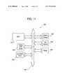
- FIG. 2illustrates a block diagram for a CMOS imager having a pixel array 200 with each pixel cell being constructed in the manner shown by element 14 of FIG. 1 .
- Pixel array 200comprises a plurality of pixels arranged in a predetermined number of columns and rows. The pixels of each row in array 200 are all turned on at the same time by a row select line and the pixels of each column are selectively output by a column select line, e.g., line 42 .
- a plurality of rows and column linesare provided for the entire array 200 .
- the row linesare selectively activated by the row driver 210 in response to row address decoder 220 and the column select lines are selectively activated by the column driver 260 in response to column address decoder 270 .
- CMOS imageris operated by the control circuit 250 which controls address decoders 220 , 270 for selecting the appropriate row and column lines for pixel readout, and row and column driver circuitry 210 , 260 which apply driving voltage to the drive transistors of the selected row and column lines.
- FIG. 3shows a simplified timing diagram for the signals used to transfer charge out of photodetector circuit 14 of the FIG. 1 CMOS imager.
- the photogate signal PGis nominally set to 5V and the reset signal RST is nominally set at 2.5V.
- the processis begun at time t 0 by briefly pulsing reset voltage RST to 5V.
- the RST voltagewhich is applied to the gate 32 of reset transistor 31 , causes transistor 31 to turn on and the floating diffusion node 30 to charge to the VDD voltage present at n+ region 34 (less the voltage drop Vth of transistor 31 ). This resets the floating diffusion node 30 to a predetermined voltage (VDD-Vth).
- the charge on floating diffusion node 30is applied to the gate of the source follower transistor 36 to control the current passing through transistor 38 , which has been turned on by a row select (ROW) signal, and load transistor 39 .
- This currentis translated into a voltage on line 42 which is next sampled by providing a SHR signal to the S/H transistor 72 which charges capacitor 74 with the source follower transistor output voltage on line 42 representing the reset charge present at floating diffusion node 30 .
- the PG signalis next pulsed to 0 volts, causing charge to be collected in n+ region 26 .
- a transfer gate voltage TXsimilar to the reset pulse RST, is then applied to transfer gate 28 of transistor 29 to cause the charge in n+ region 26 to transfer to floating diffusion node 30 .
- the transfer gate voltage TXmay be pulsed or held to a fixed DC potential.
- the transfer gate voltage TXmust be pulsed.
- the new output voltage on line 42 generated by source follower transistor 36 currentis then sampled onto capacitor 64 by enabling the sample and hold switch 62 by signal SHS.
- the column select signalis next applied to transistors 68 and 70 and the respective charges stored in capacitors 64 and 74 are subtracted in subtractor 82 to provide a pixel output signal at terminal 81 .
- CMOS imagersmay dispense with the transfer gate 28 and associated transistor 29 , or retain these structures while biasing the transfer transistor 29 to an always “on” state.
- CMOS imagerThe operation of the charge collection of the CMOS imager is known in the art and is described in several publications such as Mendis et al., “Progress in CMOS Active Pixel Image Sensors,” SPIE Vol. 2172, pp. 19-29 1994; Mendis et al., “CMOS Active Pixel Image Sensors for Highly Integrated Imaging Systems,” IEEE Journal of Solid State Circuits, Vol. 32 (2), 1997; and Eric R, Fossum, “CMOS Image Sensors: Electronic Camera on a Chip,” IEDM Vol. 95 pages 17-25 (1995) as well as other publications. These references are incorporated herein by reference.
- CMOS imagerswhich use a silicon dioxide (SiO 2 ) insulator between the photogate and the charge accumulation area beneath the photogate suffer from low capacitance, which reduces the signal to noise ratio of the imager.
- Low capacitancereduces the charge storage capacity of the accumulated electrical charge within the pixel and decreases the dynamic range of CMOS imagers. Since the size of the pixel electrical signal is very small due to the collection of photons in the photo array, the signal to noise ratio of the pixel should be as high as possible.
- a thinner SiO 2 insulatoris required. However, if the insulator layer is too thin it inhibits proper operation of the photogate and the various transistor gates of the imager by the creation of pinhole defects, gate to substrate leakage and low breakdown voltage of the insulator.
- the present inventionprovides an imaging device formed as a CMOS integrated circuit using a standard CMOS process.
- the imager circuitincludes a floating diffusion region which is connected to a gate of a source follower transistor.
- the CMOS imagerincludes a nitride, nitride/oxide or ONO insulating material between diffusion regions in the substrate and overlying gate area of the photogate.
- the nitrogen containing insulating materialprovides increased capacitance in the CMOS imager, better breakdown voltage than prior SiO 2 insulators, better breakdown voltage characteristics between the photogate and transfer gate for the case of a photogate overlapping the transfer gate, and a wider dynamic range and an improved signal to noise ratio.
- the higher breakdown voltagealso allows the imager photogate to operate at higher potentials with a further increase in charge storage capacity.
- FIG. 1is a representative circuit of a CMOS imager.
- FIG. 2is a block diagram of a CMOS active pixel sensor chip.
- FIG. 3is a representative timing diagram for the CMOS imager.
- FIG. 4illustrates a partially cut away side view of a portion of a semiconductor CMOS imager wafer in an interim stage of processing.
- FIG. 5illustrates a partially cut away side view of a portion of a semiconductor CMOS imager wafer subsequent to FIG. 4 .
- FIG. 6illustrates a partially cut away side view of a portion of a semiconductor CMOS imager wafer subsequent to FIG. 5 .
- FIG. 7illustrates a partially cut away side view of a portion of a semiconductor CMOS imager wafer subsequent to FIG. 6 .
- FIG. 8illustrates a partially cut away side view of a portion of a semiconductor CMOS imager wafer subsequent to FIG. 7 .
- FIG. 9illustrates a partially cut away side view of a portion of a semiconductor CMOS imager wafer subsequent to FIG. 8 .
- FIG. 10illustrates a partially cut away side view of a portion of a semiconductor CMOS imager wafer subsequent to FIG. 9 .
- FIG. 11is an illustration of a computer system having a CMOS imager according to the present invention.
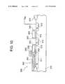
- FIG. 4This figure shows a portion of a CMOS imager 300 at one point in the fabrication process.
- the substrate 310has field oxide regions 341 formed to surround and isolate the cells which may be formed by thermal oxidation.
- a first insulating layer 315is grown over a surface of substrate 310 .
- the first insulating layer 315is a silicon dioxide layer which may be formed, i.e., grown, by conventional methods.
- the first insulating layer 315is grown by thermal oxidation of silicon and the first insulating layer 315 has a thickness of from about 30 to about 500 angstroms.
- a transfer gate stack 320 and a reset gate stack 325are deposited and patterned over the first insulating layer 315 as shown in FIG. 5 .
- the gate stacks 320 , 325include a doped polysilicon layer on insulating layer 315 , or a doped polysilicon layer with a silicide layer on top of the polysilicon on the insulating layer 315 or a doped polysilicon/silicide/insulator on the insulating layer 315 , or the gate stacks 320 , 325 may be formed of any material known to form a gate electrode.
- An insulating layer 343is formed, i.e., grown, on the edges of the exposed polysilicon gate stacks 320 , 325 and anisotropically etched to remove the insulator deposited on the horizontal surfaces as shown in FIG. 6 .
- the insulating layer 343is a deposited oxide or nitride.
- the first insulating layer 315is partly or wholly removed from the substrate by etching such that it only remains under gate stacks 320 and 325 .
- the doped regions 312 and 313are then formed in the substrate 310 as shown in FIG. 7 . Any suitable doping process may be used, such as, for example, ion implantation.
- a resist and mask(not shown) may be used to shield other areas that are not to be doped.
- Doped region 311may also formed in this step. The region 311 may be formed in a similar manner to doped regions 312 and 313 .
- the doped region 311may be formed with the same mask used for forming doped regions 312 and 313 or doped region 311 may be formed using a separate mask in an additional step. After the doped regions 311 , 312 and 313 are formed, thermal processing is used to fully form regions 311 , 312 and 313 under portions of the gate stacks 320 and 325 as shown in FIG. 7 .
- a nitrogen containing insulating layer 330is then deposited onto the substrate as illustrated in FIG. 8 .
- the nitrogen containing insulating layer 330is preferably a silicon nitride layer, a nitride oxide (NO) layer, an oxide/nitride (ON) layer or an ONO (oxide-nitride-oxide) layer deposited by a combination of CVD and thermal oxidation.
- the first oxide layermay be thermally grown or deposited by CVD.
- the nitride layeris then typically deposited by CVD.
- the final step in forming the ONO layeris to thermally oxidize the nitride layer to form the final oxide layer.
- the nitrogen containing insulating layerhas a thickness of from about 20 to about 500 angstroms, more preferably from about 30 to about 100 angstroms.
- a second conductive layer 350is next deposited over the substrate 310 and the nitrogen containing insulating layer 330 .
- the second conductive layer 350is formed of a doped polysilicon, however any partially transparent conductive material such as indium-tin-oxide (ITO), tin oxide, indium oxide or doped hydrogenated amorphous silicon may be used.
- ITOindium-tin-oxide
- tin oxideindium oxide
- doped hydrogenated amorphous siliconmay be used.
- the second conductive layer 350is patterned and etched so that the second conductive layer 350 remains over the photogate 360 as shown in FIG. 9 .
- the deposited nitride, ON, NO, ONO filmprovides better isolation between gate 320 and conductor 350 than a grown or deposited oxide layer.
- the nitrogen containing layer 330is removed wherever it is not covered and protected by the 350 conductor as shown in FIG. 10 .
- the CMOS imager 300is processed from the device shown in FIG. 10 to an operable CMOS imager by conventional processing methods to form contacts and wiring to connect gate lines and other connections in the pixel cell.
- the entire surfacemay be covered with a passivation layer of, e.g., silicon dioxide, BPSG, PSG, BSG or the like which may be planarized, typically by CMP and etched to provide contact holes, which are then metallized to provide contacts to the gates and active area diffusions of the device.
- Conventional multiple layers of conductors and insulatorsmay also be used to interconnect the structures in the manner shown in FIG. 1 .
- the nitrogen containing layer 330increases the capacitance between the photogate 350 and underlying n-type region 311 . This improves the charge storage and signal acquisition and dynamic range of the CMOS imager sensor. The increased capacitance also provides a better signal to noise ratio, a better ability of the imager to see bright scenes and a wider dynamic range.
- FIG. 11A typical processor based system which includes a CMOS imager device according to the present invention is illustrated generally at 400 in FIG. 11 .
- the illustrated systemis exemplary of a device having digital circuits which include CMOS imager devices.
- Other types of processor systemswhich include the same or similar systems of FIG. 11 include cameras, scanners, machine vision systems, vehicle navigation systems, video telephones, computer input devices, surveillance systems, auto focus systems, star trackers, motion detection systems, image stabilization systems and data compression systems for high-definition television.
- a processor based systemsuch as a computer system, generally comprises a central processing unit (CPU) 444 that communicates with an input/output (I/O) device 446 over a bus 452 .
- the CMOS imager 442also communicates with the system over bus 452 .
- the computer system 400also includes random access memory (RAM) 448 , and may include peripheral devices such as a floppy disk drive 454 and a compact disk (CD) ROM drive 456 which also communicate with CPU 444 over the bus 452 .
- CMOS imager 442is an integrated circuit which includes a nitrogen containing insulating layer, as previously described with respect to FIGS. 4-7 .
- the CMOS imager arraycan be formed on a single chip together with the logic or the logic and array may be formed on separate IC chips.
- the inventionhas been described with reference to n-regions and an n-doped channel in a p-well, it should be understood that the present invention includes p-regions and a p-doped channel in an n-well.
- the CMOS imageris described having a transfer gate and a photogate that overlaps the transfer gate; however, the photogate need not overlap the transfer gate.
- the inventionmay also be used in CMOS imagers where no transfer gate is employed.
Landscapes
- Solid State Image Pick-Up Elements (AREA)
Abstract
Description
Claims (87)
Priority Applications (2)
| Application Number | Priority Date | Filing Date | Title |
|---|---|---|---|
| US09/172,298US7791116B1 (en) | 1998-10-14 | 1998-10-14 | CMOS imager having a nitride dielectric |
| US12/849,838US8105858B2 (en) | 1998-10-14 | 2010-08-04 | CMOS imager having a nitride dielectric |
Applications Claiming Priority (1)
| Application Number | Priority Date | Filing Date | Title |
|---|---|---|---|
| US09/172,298US7791116B1 (en) | 1998-10-14 | 1998-10-14 | CMOS imager having a nitride dielectric |
Related Child Applications (1)
| Application Number | Title | Priority Date | Filing Date |
|---|---|---|---|
| US12/849,838DivisionUS8105858B2 (en) | 1998-10-14 | 2010-08-04 | CMOS imager having a nitride dielectric |
Publications (1)
| Publication Number | Publication Date |
|---|---|
| US7791116B1true US7791116B1 (en) | 2010-09-07 |
Family
ID=42669643
Family Applications (2)
| Application Number | Title | Priority Date | Filing Date |
|---|---|---|---|
| US09/172,298Expired - Fee RelatedUS7791116B1 (en) | 1998-10-14 | 1998-10-14 | CMOS imager having a nitride dielectric |
| US12/849,838Expired - Fee RelatedUS8105858B2 (en) | 1998-10-14 | 2010-08-04 | CMOS imager having a nitride dielectric |
Family Applications After (1)
| Application Number | Title | Priority Date | Filing Date |
|---|---|---|---|
| US12/849,838Expired - Fee RelatedUS8105858B2 (en) | 1998-10-14 | 2010-08-04 | CMOS imager having a nitride dielectric |
Country Status (1)
| Country | Link |
|---|---|
| US (2) | US7791116B1 (en) |
Cited By (3)
| Publication number | Priority date | Publication date | Assignee | Title |
|---|---|---|---|---|
| US20090180010A1 (en)* | 2008-01-14 | 2009-07-16 | Adkisson James W | Low lag transfer gate device |
| US20160071900A1 (en)* | 2008-10-21 | 2016-03-10 | Intellectual Ventures Ii Llc | Backside Illuminated Image Sensor |
| US9445020B2 (en)* | 1998-06-08 | 2016-09-13 | Sony Corporation | Solid-state imaging element having image signal overflow path |
Families Citing this family (1)
| Publication number | Priority date | Publication date | Assignee | Title |
|---|---|---|---|---|
| US20240355865A1 (en)* | 2023-04-21 | 2024-10-24 | Taiwan Semiconductor Manufacturing Company, Ltd. | Semiconductor capacitor for image sensor pixel circuitry |
Citations (18)
| Publication number | Priority date | Publication date | Assignee | Title |
|---|---|---|---|---|
| US4143389A (en)* | 1976-08-16 | 1979-03-06 | Hitachi, Ltd. | Photoelectric element in a solid-state image pick-up device |
| US4374700A (en) | 1981-05-29 | 1983-02-22 | Texas Instruments Incorporated | Method of manufacturing silicide contacts for CMOS devices |
| US4385307A (en)* | 1977-04-08 | 1983-05-24 | Tokyo Shibaura Electric Co., Ltd. | Solid state image sensing device for enhanced charge carrier accumulation |
| US5241198A (en)* | 1990-11-26 | 1993-08-31 | Matsushita Electronics Corporation | Charge-coupled device and solid-state imaging device |
| US5307169A (en)* | 1991-05-07 | 1994-04-26 | Olympus Optical Co., Ltd. | Solid-state imaging device using high relative dielectric constant material as insulating film |
| US5319604A (en) | 1990-05-08 | 1994-06-07 | Texas Instruments Incorporated | Circuitry and method for selectively switching negative voltages in CMOS integrated circuits |
| US5334867A (en)* | 1992-05-11 | 1994-08-02 | Samsung Electronics Co., Ltd. | Image sensor device with insulation film |
| US5461425A (en) | 1994-02-15 | 1995-10-24 | Stanford University | CMOS image sensor with pixel level A/D conversion |
| US5471515A (en) | 1994-01-28 | 1995-11-28 | California Institute Of Technology | Active pixel sensor with intra-pixel charge transfer |
| US5541402A (en) | 1994-10-17 | 1996-07-30 | At&T Corp. | Imaging active pixel device having a non-destructive read-out gate |
| US5576763A (en) | 1994-11-22 | 1996-11-19 | Lucent Technologies Inc. | Single-polysilicon CMOS active pixel |
| US5612799A (en) | 1990-11-26 | 1997-03-18 | Semiconductor Energy Laboratory Co., Inc. | Active matrix type electro-optical device |
| US5614744A (en) | 1995-08-04 | 1997-03-25 | National Semiconductor Corporation | CMOS-based, low leakage active pixel array with anti-blooming isolation |
| US5625210A (en) | 1995-04-13 | 1997-04-29 | Eastman Kodak Company | Active pixel sensor integrated with a pinned photodiode |
| US5705846A (en) | 1995-07-31 | 1998-01-06 | National Semiconductor Corporation | CMOS-compatible active pixel image array using vertical pnp cell |
| US5708263A (en) | 1995-12-27 | 1998-01-13 | International Business Machines Corporation | Photodetector array |
| US5757045A (en) | 1996-07-17 | 1998-05-26 | Taiwan Semiconductor Manufacturing Company Ltd. | CMOS device structure with reduced risk of salicide bridging and reduced resistance via use of a ultra shallow, junction extension, ion implantation |
| US5804845A (en)* | 1996-10-08 | 1998-09-08 | Eastman Kodak Company | Image sensor having ITO electrodes with an ONO layer |
Family Cites Families (2)
| Publication number | Priority date | Publication date | Assignee | Title |
|---|---|---|---|---|
| JP2568145Y2 (en)* | 1992-08-14 | 1998-04-08 | 株式会社アドバンテスト | Signal time difference measuring device |
| US6376868B1 (en)* | 1999-06-15 | 2002-04-23 | Micron Technology, Inc. | Multi-layered gate for a CMOS imager |
- 1998
- 1998-10-14USUS09/172,298patent/US7791116B1/ennot_activeExpired - Fee Related
- 2010
- 2010-08-04USUS12/849,838patent/US8105858B2/ennot_activeExpired - Fee Related
Patent Citations (19)
| Publication number | Priority date | Publication date | Assignee | Title |
|---|---|---|---|---|
| US4143389A (en)* | 1976-08-16 | 1979-03-06 | Hitachi, Ltd. | Photoelectric element in a solid-state image pick-up device |
| US4385307A (en)* | 1977-04-08 | 1983-05-24 | Tokyo Shibaura Electric Co., Ltd. | Solid state image sensing device for enhanced charge carrier accumulation |
| US4374700A (en) | 1981-05-29 | 1983-02-22 | Texas Instruments Incorporated | Method of manufacturing silicide contacts for CMOS devices |
| US5319604A (en) | 1990-05-08 | 1994-06-07 | Texas Instruments Incorporated | Circuitry and method for selectively switching negative voltages in CMOS integrated circuits |
| US5612799A (en) | 1990-11-26 | 1997-03-18 | Semiconductor Energy Laboratory Co., Inc. | Active matrix type electro-optical device |
| US5241198A (en)* | 1990-11-26 | 1993-08-31 | Matsushita Electronics Corporation | Charge-coupled device and solid-state imaging device |
| US5307169A (en)* | 1991-05-07 | 1994-04-26 | Olympus Optical Co., Ltd. | Solid-state imaging device using high relative dielectric constant material as insulating film |
| US5334867B1 (en)* | 1992-05-11 | 1996-06-25 | Samsung Electronics Co Ltd | Image sensor device with insulation film |
| US5334867A (en)* | 1992-05-11 | 1994-08-02 | Samsung Electronics Co., Ltd. | Image sensor device with insulation film |
| US5471515A (en) | 1994-01-28 | 1995-11-28 | California Institute Of Technology | Active pixel sensor with intra-pixel charge transfer |
| US5461425A (en) | 1994-02-15 | 1995-10-24 | Stanford University | CMOS image sensor with pixel level A/D conversion |
| US5541402A (en) | 1994-10-17 | 1996-07-30 | At&T Corp. | Imaging active pixel device having a non-destructive read-out gate |
| US5576763A (en) | 1994-11-22 | 1996-11-19 | Lucent Technologies Inc. | Single-polysilicon CMOS active pixel |
| US5625210A (en) | 1995-04-13 | 1997-04-29 | Eastman Kodak Company | Active pixel sensor integrated with a pinned photodiode |
| US5705846A (en) | 1995-07-31 | 1998-01-06 | National Semiconductor Corporation | CMOS-compatible active pixel image array using vertical pnp cell |
| US5614744A (en) | 1995-08-04 | 1997-03-25 | National Semiconductor Corporation | CMOS-based, low leakage active pixel array with anti-blooming isolation |
| US5708263A (en) | 1995-12-27 | 1998-01-13 | International Business Machines Corporation | Photodetector array |
| US5757045A (en) | 1996-07-17 | 1998-05-26 | Taiwan Semiconductor Manufacturing Company Ltd. | CMOS device structure with reduced risk of salicide bridging and reduced resistance via use of a ultra shallow, junction extension, ion implantation |
| US5804845A (en)* | 1996-10-08 | 1998-09-08 | Eastman Kodak Company | Image sensor having ITO electrodes with an ONO layer |
Non-Patent Citations (25)
| Title |
|---|
| Dickinson, A., et al., A 256×256 CMOS Active Pixel Image Sensor with Motion Detection, 1995 IEEE International Solid-State Circuits Conference, pp. 226-227. |
| Dickinson, A., et al., Standard CMOS Active Pixel Image Sensors for Multimedia Applications, Proceedings of Sixteenth Conference on Advanced Research in VLSI, Mar. 27-29, 1995, pp. 214-224. |
| Eid, E-S., et al., A 256×256 CMOS Active Pixel Image Sensor, Proc. SPIE vol. 2415, Apr. 1995, pp. 265-275. |
| Fossum, E., Architectures for focal plane image processing, Optical Engineering, vol. 28, No. 8, Aug. 1989, pp. 865-871. |
| Fossum, E., CMOS Image Sensors: Electronic Camera on a Chip, 1995 IEEE, pp. 17-25, IEDM. |
| Fossum, E., et al., IEDM A 37×28mm2 600k-Pixel CMOS APS Dental X-Ray Camera-on-a-Chip with Self-Triggered Readout, 1998 IEEE International Solid-State Circuits Conference, pp. 172-173. |
| Fossum, E., Low Power Camera-on-a-Chip Using CMOS Active Pixel Sensor Technology, 1995 IEEE, pp. 74-77, IEDM. |
| Janesick, J., et al., New advancements in charge-coupled device technology-sub-electron noise and 4096×4096 pixel CCDs, Proc. SPIE vol. 1242, 1990, pp. 223-237. |
| Janesick, J., et al., New advancements in charge-coupled device technology—sub-electron noise and 4096×4096 pixel CCDs, Proc. SPIE vol. 1242, 1990, pp. 223-237. |
| Kemeny, S.E., et al., Update on focal-plane image processing research, Proc. SPIE vol. 1447, 1991, pp. 243-250. |
| Mendis, S., et al., CMOS Active Pixel Image Sensor, IEEE Transactions on Electron Devices, vol. 41, No. 3, Mar. 1994, pp. 452-453. |
| Mendis, S.K., et al., A 128×128 CMOS Active Pixel Image Sensor for Highly Integrated Imaging Systems, 1993 IEEE, pp. 583-586, IEDM. |
| Mendis, S.K., et al., CMOS Active Pixel Image Sensors for Highly Integrated Imaging Systems, IEEE Journal of Solid-State Circuits, vol. 32, No. 2, Feb. 1997, pp. 187-197. |
| Mendis, S.K., et al., Low-Light-Level Image Sensor with On-Chip Signal Processing, Proc. SPIE vol. 1952, Nov. 1993, pp. 23-33. |
| Mendis, S.K., et al., Progress in CMOS Active Pixel Image Sensors, Proc. SPIE vol. 2172, May 1994, pp. 19-29. |
| Nakamura, J., et al., CMOS Active Pixel Image Sensor with Simple Floating Gate Pixels, IEEE Transactions on Electron Devices, vol. 42, No. 9, Sep. 1995, pp. 1693-1694. |
| Nixon, R.H., et al., 256×256 CMOS Active Pixel Sensor Camera-on-a-Chip, 1996 IEEE International Solid-State Circuits Conference, pp. 178-179. |
| Nixon, R.H., et al., 256×256 CMOS Active Pixel Sensor Camera-on-a-Chip, IEEE Journal of Solid-State Circuits, vol. 31, No. 12, Dec. 1996, pp. 2046-2050. |
| Panicacci, R., et al., Programmable multiresolution CMOS active pixel sensor, Proc. SPIE vol. 2654, Mar. 1996, pp. 72-79. |
| Panicacci, R.A., et al., 128Mb/s Multiport CMOS Binary Active-Pixel Image Sensor, 1996 IEEE International Solid-State Circuit Conference, pp. 100-101. |
| Yadid-Pecht, O., et al., CMOS Active Pixel Sensor Star Tracker with Regional Electronic Shutter, IEEE Journal of Solid-State Circuits, vol. 32, No. 2, Feb. 1997, pp. 285-288. |
| Yadid-Pecht, O., et al., Wide dynamic range APS star tracker, Proc. SPIE vol. 2654, Mar. 1996, pp. 82-92. |
| Zarnowski, J., et al., Imaging options expand with CMOS technology, Laser Focus World, Jun. 1997, pp. 125-130. |
| Zhou, Z., et al., A CMOS Imager with On-Chip Variable Resolution for Light-Adaptive Imaging, 1998 IEEE International Solid-State Circuits Conference, pp. 174-175. |
| Zhou, Z., et al., A Digital CMOS Active Pixel Image Sensor for Multimedia Applications, Proc. SPIE vol. 2894, Sep. 1996, pp. 282-288. |
Cited By (5)
| Publication number | Priority date | Publication date | Assignee | Title |
|---|---|---|---|---|
| US9445020B2 (en)* | 1998-06-08 | 2016-09-13 | Sony Corporation | Solid-state imaging element having image signal overflow path |
| US20090180010A1 (en)* | 2008-01-14 | 2009-07-16 | Adkisson James W | Low lag transfer gate device |
| US8743247B2 (en)* | 2008-01-14 | 2014-06-03 | International Business Machines Corporation | Low lag transfer gate device |
| US20160071900A1 (en)* | 2008-10-21 | 2016-03-10 | Intellectual Ventures Ii Llc | Backside Illuminated Image Sensor |
| US10020338B2 (en)* | 2008-10-21 | 2018-07-10 | Intellectual Ventures Ii Llc | Backside illuminated image sensor |
Also Published As
| Publication number | Publication date |
|---|---|
| US8105858B2 (en) | 2012-01-31 |
| US20100297807A1 (en) | 2010-11-25 |
Similar Documents
| Publication | Publication Date | Title |
|---|---|---|
| US6723594B2 (en) | Pixel cell with high storage capacitance for a CMOS imager | |
| US7405101B2 (en) | CMOS imager with selectively silicided gate | |
| US6500692B1 (en) | Method of making trench photosensor for a CMOS imager | |
| US6429470B1 (en) | CMOS imager with storage capacitor | |
| US7091059B2 (en) | Method of forming a photosensor comprising a plurality of trenches | |
| US6376868B1 (en) | Multi-layered gate for a CMOS imager | |
| US6967121B2 (en) | Buried channel CMOS imager and method of forming same | |
| US7655494B2 (en) | Trench photosensor for a CMOS imager | |
| US7224009B2 (en) | Method for forming a low leakage contact in a CMOS imager | |
| US6291280B1 (en) | CMOS imager cell having a buried contact and method of fabrication | |
| US6414342B1 (en) | Photogate with improved short wavelength response for a CMOS imager | |
| US8105858B2 (en) | CMOS imager having a nitride dielectric |
Legal Events
| Date | Code | Title | Description |
|---|---|---|---|
| AS | Assignment | Owner name:MICRON TECHNOLOGY, INC., IDAHO Free format text:ASSIGNMENT OF ASSIGNORS INTEREST;ASSIGNOR:RHODES, HOWARD E.;REEL/FRAME:009520/0715 Effective date:19981012 | |
| FEPP | Fee payment procedure | Free format text:PAYOR NUMBER ASSIGNED (ORIGINAL EVENT CODE: ASPN); ENTITY STATUS OF PATENT OWNER: LARGE ENTITY | |
| STCF | Information on status: patent grant | Free format text:PATENTED CASE | |
| FPAY | Fee payment | Year of fee payment:4 | |
| AS | Assignment | Owner name:U.S. BANK NATIONAL ASSOCIATION, AS COLLATERAL AGENT, CALIFORNIA Free format text:SECURITY INTEREST;ASSIGNOR:MICRON TECHNOLOGY, INC.;REEL/FRAME:038669/0001 Effective date:20160426 Owner name:U.S. BANK NATIONAL ASSOCIATION, AS COLLATERAL AGEN Free format text:SECURITY INTEREST;ASSIGNOR:MICRON TECHNOLOGY, INC.;REEL/FRAME:038669/0001 Effective date:20160426 | |
| AS | Assignment | Owner name:MORGAN STANLEY SENIOR FUNDING, INC., AS COLLATERAL AGENT, MARYLAND Free format text:PATENT SECURITY AGREEMENT;ASSIGNOR:MICRON TECHNOLOGY, INC.;REEL/FRAME:038954/0001 Effective date:20160426 Owner name:MORGAN STANLEY SENIOR FUNDING, INC., AS COLLATERAL Free format text:PATENT SECURITY AGREEMENT;ASSIGNOR:MICRON TECHNOLOGY, INC.;REEL/FRAME:038954/0001 Effective date:20160426 | |
| AS | Assignment | Owner name:U.S. BANK NATIONAL ASSOCIATION, AS COLLATERAL AGENT, CALIFORNIA Free format text:CORRECTIVE ASSIGNMENT TO CORRECT THE REPLACE ERRONEOUSLY FILED PATENT #7358718 WITH THE CORRECT PATENT #7358178 PREVIOUSLY RECORDED ON REEL 038669 FRAME 0001. ASSIGNOR(S) HEREBY CONFIRMS THE SECURITY INTEREST;ASSIGNOR:MICRON TECHNOLOGY, INC.;REEL/FRAME:043079/0001 Effective date:20160426 Owner name:U.S. BANK NATIONAL ASSOCIATION, AS COLLATERAL AGEN Free format text:CORRECTIVE ASSIGNMENT TO CORRECT THE REPLACE ERRONEOUSLY FILED PATENT #7358718 WITH THE CORRECT PATENT #7358178 PREVIOUSLY RECORDED ON REEL 038669 FRAME 0001. ASSIGNOR(S) HEREBY CONFIRMS THE SECURITY INTEREST;ASSIGNOR:MICRON TECHNOLOGY, INC.;REEL/FRAME:043079/0001 Effective date:20160426 | |
| MAFP | Maintenance fee payment | Free format text:PAYMENT OF MAINTENANCE FEE, 8TH YEAR, LARGE ENTITY (ORIGINAL EVENT CODE: M1552) Year of fee payment:8 | |
| AS | Assignment | Owner name:JPMORGAN CHASE BANK, N.A., AS COLLATERAL AGENT, ILLINOIS Free format text:SECURITY INTEREST;ASSIGNORS:MICRON TECHNOLOGY, INC.;MICRON SEMICONDUCTOR PRODUCTS, INC.;REEL/FRAME:047540/0001 Effective date:20180703 Owner name:JPMORGAN CHASE BANK, N.A., AS COLLATERAL AGENT, IL Free format text:SECURITY INTEREST;ASSIGNORS:MICRON TECHNOLOGY, INC.;MICRON SEMICONDUCTOR PRODUCTS, INC.;REEL/FRAME:047540/0001 Effective date:20180703 | |
| AS | Assignment | Owner name:MICRON TECHNOLOGY, INC., IDAHO Free format text:RELEASE BY SECURED PARTY;ASSIGNOR:U.S. BANK NATIONAL ASSOCIATION, AS COLLATERAL AGENT;REEL/FRAME:047243/0001 Effective date:20180629 | |
| AS | Assignment | Owner name:MICRON TECHNOLOGY, INC., IDAHO Free format text:RELEASE BY SECURED PARTY;ASSIGNOR:MORGAN STANLEY SENIOR FUNDING, INC., AS COLLATERAL AGENT;REEL/FRAME:050937/0001 Effective date:20190731 | |
| AS | Assignment | Owner name:MICRON SEMICONDUCTOR PRODUCTS, INC., IDAHO Free format text:RELEASE BY SECURED PARTY;ASSIGNOR:JPMORGAN CHASE BANK, N.A., AS COLLATERAL AGENT;REEL/FRAME:051028/0001 Effective date:20190731 Owner name:MICRON TECHNOLOGY, INC., IDAHO Free format text:RELEASE BY SECURED PARTY;ASSIGNOR:JPMORGAN CHASE BANK, N.A., AS COLLATERAL AGENT;REEL/FRAME:051028/0001 Effective date:20190731 | |
| FEPP | Fee payment procedure | Free format text:MAINTENANCE FEE REMINDER MAILED (ORIGINAL EVENT CODE: REM.); ENTITY STATUS OF PATENT OWNER: LARGE ENTITY | |
| LAPS | Lapse for failure to pay maintenance fees | Free format text:PATENT EXPIRED FOR FAILURE TO PAY MAINTENANCE FEES (ORIGINAL EVENT CODE: EXP.); ENTITY STATUS OF PATENT OWNER: LARGE ENTITY | |
| STCH | Information on status: patent discontinuation | Free format text:PATENT EXPIRED DUE TO NONPAYMENT OF MAINTENANCE FEES UNDER 37 CFR 1.362 | |
| FP | Lapsed due to failure to pay maintenance fee | Effective date:20220907 |