US7790633B1 - Sequential deposition/anneal film densification method - Google Patents
Sequential deposition/anneal film densification methodDownload PDFInfo
- Publication number
- US7790633B1 US7790633B1US11/519,445US51944506AUS7790633B1US 7790633 B1US7790633 B1US 7790633B1US 51944506 AUS51944506 AUS 51944506AUS 7790633 B1US7790633 B1US 7790633B1
- Authority
- US
- United States
- Prior art keywords
- annealing
- dielectric film
- layer
- substrate
- catalyst
- Prior art date
- Legal status (The legal status is an assumption and is not a legal conclusion. Google has not performed a legal analysis and makes no representation as to the accuracy of the status listed.)
- Active, expires
Links
- 238000000034methodMethods0.000titleclaimsabstractdescription154
- 230000008021depositionEffects0.000titleabstractdescription44
- 238000000280densificationMethods0.000titledescription14
- 230000008569processEffects0.000claimsabstractdescription88
- 239000000758substrateSubstances0.000claimsabstractdescription80
- VYPSYNLAJGMNEJ-UHFFFAOYSA-NSilicium dioxideChemical compoundO=[Si]=OVYPSYNLAJGMNEJ-UHFFFAOYSA-N0.000claimsabstractdescription66
- 238000000137annealingMethods0.000claimsabstractdescription60
- XLYOFNOQVPJJNP-UHFFFAOYSA-NwaterSubstancesOXLYOFNOQVPJJNP-UHFFFAOYSA-N0.000claimsabstractdescription37
- 239000003795chemical substances by applicationSubstances0.000claimsabstractdescription13
- 238000013508migrationMethods0.000claimsabstractdescription6
- 230000005012migrationEffects0.000claimsabstractdescription6
- 230000035515penetrationEffects0.000claimsabstractdescription6
- 239000007789gasSubstances0.000claimsdescription70
- 239000002243precursorSubstances0.000claimsdescription58
- 238000000151depositionMethods0.000claimsdescription51
- 239000003054catalystSubstances0.000claimsdescription32
- XUIMIQQOPSSXEZ-UHFFFAOYSA-NSiliconChemical compound[Si]XUIMIQQOPSSXEZ-UHFFFAOYSA-N0.000claimsdescription24
- 229910052710siliconInorganic materials0.000claimsdescription24
- 239000010703siliconSubstances0.000claimsdescription24
- QVGXLLKOCUKJST-UHFFFAOYSA-Natomic oxygenChemical compound[O]QVGXLLKOCUKJST-UHFFFAOYSA-N0.000claimsdescription20
- 239000001301oxygenSubstances0.000claimsdescription20
- 229910052760oxygenInorganic materials0.000claimsdescription20
- 229910052814silicon oxideInorganic materials0.000claimsdescription16
- 229910052782aluminiumInorganic materials0.000claimsdescription15
- XAGFODPZIPBFFR-UHFFFAOYSA-NaluminiumChemical compound[Al]XAGFODPZIPBFFR-UHFFFAOYSA-N0.000claimsdescription15
- 229910052751metalInorganic materials0.000claimsdescription15
- 239000002184metalSubstances0.000claimsdescription15
- 230000001590oxidative effectEffects0.000claimsdescription14
- 238000000231atomic layer depositionMethods0.000claimsdescription11
- 239000004065semiconductorSubstances0.000claimsdescription10
- GQPLMRYTRLFLPF-UHFFFAOYSA-NNitrous OxideChemical compound[O-][N+]#NGQPLMRYTRLFLPF-UHFFFAOYSA-N0.000claimsdescription6
- HOXINJBQVZWYGZ-UHFFFAOYSA-Nfenbutatin oxideChemical compoundC=1C=CC=CC=1C(C)(C)C[Sn](O[Sn](CC(C)(C)C=1C=CC=CC=1)(CC(C)(C)C=1C=CC=CC=1)CC(C)(C)C=1C=CC=CC=1)(CC(C)(C)C=1C=CC=CC=1)CC(C)(C)C1=CC=CC=C1HOXINJBQVZWYGZ-UHFFFAOYSA-N0.000claimsdescription3
- 238000011065in-situ storageMethods0.000claimsdescription3
- JLTRXTDYQLMHGR-UHFFFAOYSA-NtrimethylaluminiumChemical compoundC[Al](C)CJLTRXTDYQLMHGR-UHFFFAOYSA-N0.000claimsdescription3
- GYHNNYVSQQEPJS-UHFFFAOYSA-NGalliumChemical compound[Ga]GYHNNYVSQQEPJS-UHFFFAOYSA-N0.000claimsdescription2
- CBENFWSGALASAD-UHFFFAOYSA-NOzoneChemical compound[O-][O+]=OCBENFWSGALASAD-UHFFFAOYSA-N0.000claimsdescription2
- RTAQQCXQSZGOHL-UHFFFAOYSA-NTitaniumChemical compound[Ti]RTAQQCXQSZGOHL-UHFFFAOYSA-N0.000claimsdescription2
- QCWXUUIWCKQGHC-UHFFFAOYSA-NZirconiumChemical compound[Zr]QCWXUUIWCKQGHC-UHFFFAOYSA-N0.000claimsdescription2
- 125000002147dimethylamino groupChemical group[H]C([H])([H])N(*)C([H])([H])[H]0.000claimsdescription2
- 229910052733galliumInorganic materials0.000claimsdescription2
- 229910052735hafniumInorganic materials0.000claimsdescription2
- VBJZVLUMGGDVMO-UHFFFAOYSA-Nhafnium atomChemical compound[Hf]VBJZVLUMGGDVMO-UHFFFAOYSA-N0.000claimsdescription2
- 229910052758niobiumInorganic materials0.000claimsdescription2
- 239000010955niobiumSubstances0.000claimsdescription2
- GUCVJGMIXFAOAE-UHFFFAOYSA-Nniobium atomChemical compound[Nb]GUCVJGMIXFAOAE-UHFFFAOYSA-N0.000claimsdescription2
- 239000001272nitrous oxideSubstances0.000claimsdescription2
- 150000002978peroxidesChemical class0.000claimsdescription2
- KCIKCCHXZMLVDE-UHFFFAOYSA-NsilanediolChemical compoundO[SiH2]OKCIKCCHXZMLVDE-UHFFFAOYSA-N0.000claimsdescription2
- SCPYDCQAZCOKTP-UHFFFAOYSA-NsilanolChemical compound[SiH3]OSCPYDCQAZCOKTP-UHFFFAOYSA-N0.000claimsdescription2
- 229910052715tantalumInorganic materials0.000claimsdescription2
- GUVRBAGPIYLISA-UHFFFAOYSA-Ntantalum atomChemical compound[Ta]GUVRBAGPIYLISA-UHFFFAOYSA-N0.000claimsdescription2
- 239000010936titaniumSubstances0.000claimsdescription2
- 229910052719titaniumInorganic materials0.000claimsdescription2
- 229910052726zirconiumInorganic materials0.000claimsdescription2
- 238000009832plasma treatmentMethods0.000claims3
- 238000002230thermal chemical vapour depositionMethods0.000claims1
- 239000000377silicon dioxideSubstances0.000abstractdescription24
- 235000012239silicon dioxideNutrition0.000abstractdescription8
- 239000010408filmSubstances0.000description124
- 239000010410layerSubstances0.000description54
- 238000006243chemical reactionMethods0.000description14
- 239000000376reactantSubstances0.000description14
- 230000015572biosynthetic processEffects0.000description13
- 238000005229chemical vapour depositionMethods0.000description11
- 239000000463materialSubstances0.000description11
- NJPPVKZQTLUDBO-UHFFFAOYSA-NnovaluronChemical compoundC1=C(Cl)C(OC(F)(F)C(OC(F)(F)F)F)=CC=C1NC(=O)NC(=O)C1=C(F)C=CC=C1FNJPPVKZQTLUDBO-UHFFFAOYSA-N0.000description11
- 229920006395saturated elastomerPolymers0.000description11
- 238000007740vapor depositionMethods0.000description9
- NBIIXXVUZAFLBC-UHFFFAOYSA-NPhosphoric acidChemical compoundOP(O)(O)=ONBIIXXVUZAFLBC-UHFFFAOYSA-N0.000description8
- 238000010586diagramMethods0.000description8
- 238000012545processingMethods0.000description8
- 230000005855radiationEffects0.000description7
- 239000002356single layerSubstances0.000description7
- 230000008901benefitEffects0.000description6
- 239000000203mixtureSubstances0.000description6
- 238000010926purgeMethods0.000description6
- -1acidic compoundsChemical class0.000description5
- 229910052786argonInorganic materials0.000description5
- 230000003197catalytic effectEffects0.000description5
- 238000005516engineering processMethods0.000description5
- 239000013529heat transfer fluidSubstances0.000description5
- XKRFYHLGVUSROY-UHFFFAOYSA-NArgonChemical compound[Ar]XKRFYHLGVUSROY-UHFFFAOYSA-N0.000description4
- IJGRMHOSHXDMSA-UHFFFAOYSA-NAtomic nitrogenChemical compoundN#NIJGRMHOSHXDMSA-UHFFFAOYSA-N0.000description4
- 229910020175SiOHInorganic materials0.000description4
- 150000007513acidsChemical class0.000description4
- 239000013626chemical specieSubstances0.000description4
- 238000009792diffusion processMethods0.000description4
- 230000000694effectsEffects0.000description4
- 229910052734heliumInorganic materials0.000description4
- 239000011261inert gasSubstances0.000description4
- 238000004519manufacturing processMethods0.000description4
- 239000007800oxidant agentSubstances0.000description4
- 239000010409thin filmSubstances0.000description4
- QTBSBXVTEAMEQO-UHFFFAOYSA-NAcetic acidChemical compoundCC(O)=OQTBSBXVTEAMEQO-UHFFFAOYSA-N0.000description3
- 229910000147aluminium phosphateInorganic materials0.000description3
- 150000001875compoundsChemical class0.000description3
- 238000013461designMethods0.000description3
- 238000011049fillingMethods0.000description3
- 239000007791liquid phaseSubstances0.000description3
- 230000007246mechanismEffects0.000description3
- 239000012071phaseSubstances0.000description3
- 238000006116polymerization reactionMethods0.000description3
- UFHFLCQGNIYNRP-UHFFFAOYSA-NHydrogenChemical compound[H][H]UFHFLCQGNIYNRP-UHFFFAOYSA-N0.000description2
- 239000002253acidSubstances0.000description2
- 125000000217alkyl groupChemical group0.000description2
- VSCWAEJMTAWNJL-UHFFFAOYSA-Kaluminium trichlorideChemical compoundCl[Al](Cl)ClVSCWAEJMTAWNJL-UHFFFAOYSA-K0.000description2
- 150000008064anhydridesChemical class0.000description2
- 239000005380borophosphosilicate glassSubstances0.000description2
- 229910052681coesiteInorganic materials0.000description2
- 229910052906cristobaliteInorganic materials0.000description2
- 238000005034decorationMethods0.000description2
- 238000005137deposition processMethods0.000description2
- WLIGPBOVYTVHKD-UHFFFAOYSA-Ndihydroxy-bis[(2-methylpropan-2-yl)oxy]silaneChemical compoundCC(C)(C)O[Si](O)(O)OC(C)(C)CWLIGPBOVYTVHKD-UHFFFAOYSA-N0.000description2
- 238000010894electron beam technologyMethods0.000description2
- 238000005530etchingMethods0.000description2
- 239000011521glassSubstances0.000description2
- 239000001257hydrogenSubstances0.000description2
- 229910052739hydrogenInorganic materials0.000description2
- ORJFXWYTRPGGRK-UHFFFAOYSA-Nhydroxy-tris(2-methylbutan-2-yloxy)silaneChemical compoundCCC(C)(C)O[Si](O)(OC(C)(C)CC)OC(C)(C)CCORJFXWYTRPGGRK-UHFFFAOYSA-N0.000description2
- HLDBBQREZCVBMA-UHFFFAOYSA-Nhydroxy-tris[(2-methylpropan-2-yl)oxy]silaneChemical compoundCC(C)(C)O[Si](O)(OC(C)(C)C)OC(C)(C)CHLDBBQREZCVBMA-UHFFFAOYSA-N0.000description2
- 230000006872improvementEffects0.000description2
- 230000010354integrationEffects0.000description2
- 238000002955isolationMethods0.000description2
- 239000007788liquidSubstances0.000description2
- 150000007522mineralic acidsChemical class0.000description2
- 238000012986modificationMethods0.000description2
- 230000004048modificationEffects0.000description2
- 229910052757nitrogenInorganic materials0.000description2
- 230000006911nucleationEffects0.000description2
- 238000010899nucleationMethods0.000description2
- 150000007524organic acidsChemical class0.000description2
- 235000005985organic acidsNutrition0.000description2
- 230000003647oxidationEffects0.000description2
- 238000007254oxidation reactionMethods0.000description2
- TWNQGVIAIRXVLR-UHFFFAOYSA-Noxo(oxoalumanyloxy)alumaneChemical compoundO=[Al]O[Al]=OTWNQGVIAIRXVLR-UHFFFAOYSA-N0.000description2
- 239000005360phosphosilicate glassSubstances0.000description2
- 238000000623plasma-assisted chemical vapour depositionMethods0.000description2
- 229910021420polycrystalline siliconInorganic materials0.000description2
- 229920005591polysiliconPolymers0.000description2
- 238000011160researchMethods0.000description2
- 150000004819silanolsChemical class0.000description2
- 229910021332silicideInorganic materials0.000description2
- FVBUAEGBCNSCDD-UHFFFAOYSA-Nsilicide(4-)Chemical compound[Si-4]FVBUAEGBCNSCDD-UHFFFAOYSA-N0.000description2
- 229910052682stishoviteInorganic materials0.000description2
- 239000000126substanceSubstances0.000description2
- 239000002344surface layerSubstances0.000description2
- 238000012546transferMethods0.000description2
- 229910052905tridymiteInorganic materials0.000description2
- OKTJSMMVPCPJKN-UHFFFAOYSA-NCarbonChemical compound[C]OKTJSMMVPCPJKN-UHFFFAOYSA-N0.000description1
- 229910018557Si OInorganic materials0.000description1
- UBGLVJVWWRDJDL-UHFFFAOYSA-K[B+3].[O-]S(=O)(=O)C(F)(F)F.[O-]S(=O)(=O)C(F)(F)F.[O-]S(=O)(=O)C(F)(F)FChemical class[B+3].[O-]S(=O)(=O)C(F)(F)F.[O-]S(=O)(=O)C(F)(F)F.[O-]S(=O)(=O)C(F)(F)FUBGLVJVWWRDJDL-UHFFFAOYSA-K0.000description1
- 238000009825accumulationMethods0.000description1
- 230000001154acute effectEffects0.000description1
- 125000003545alkoxy groupChemical group0.000description1
- 150000003973alkyl aminesChemical class0.000description1
- ILRRQNADMUWWFW-UHFFFAOYSA-Kaluminium phosphateChemical compoundO1[Al]2OP1(=O)O2ILRRQNADMUWWFW-UHFFFAOYSA-K0.000description1
- 150000003863ammonium saltsChemical class0.000description1
- 150000004982aromatic aminesChemical class0.000description1
- 150000001543aryl boronic acidsChemical class0.000description1
- ZSTLPJLUQNQBDQ-UHFFFAOYSA-Nazanylidyne(dihydroxy)-$l^{5}-phosphaneChemical classOP(O)#NZSTLPJLUQNQBDQ-UHFFFAOYSA-N0.000description1
- 238000006664bond formation reactionMethods0.000description1
- 239000006227byproductSubstances0.000description1
- 229910052799carbonInorganic materials0.000description1
- 239000007795chemical reaction productSubstances0.000description1
- 239000004020conductorSubstances0.000description1
- 230000008878couplingEffects0.000description1
- 238000010168coupling processMethods0.000description1
- 238000005859coupling reactionMethods0.000description1
- 238000004132cross linkingMethods0.000description1
- 230000003247decreasing effectEffects0.000description1
- 230000001419dependent effectEffects0.000description1
- 239000003989dielectric materialSubstances0.000description1
- 238000007598dipping methodMethods0.000description1
- 230000005284excitationEffects0.000description1
- 230000008570general processEffects0.000description1
- 229910052736halogenInorganic materials0.000description1
- 150000002367halogensChemical class0.000description1
- 239000001307heliumSubstances0.000description1
- SWQJXJOGLNCZEY-UHFFFAOYSA-Nhelium atomChemical compound[He]SWQJXJOGLNCZEY-UHFFFAOYSA-N0.000description1
- BHEPBYXIRTUNPN-UHFFFAOYSA-Nhydridophosphorus(.) (triplet)Chemical compound[PH]BHEPBYXIRTUNPN-UHFFFAOYSA-N0.000description1
- 125000002887hydroxy groupChemical group[H]O*0.000description1
- AQBHYBKXRJGURC-UHFFFAOYSA-Nhydroxy-methyl-bis(2-methylbutan-2-yloxy)silaneChemical compoundCCC(C)(C)O[Si](C)(O)OC(C)(C)CCAQBHYBKXRJGURC-UHFFFAOYSA-N0.000description1
- 238000010348incorporationMethods0.000description1
- 238000002347injectionMethods0.000description1
- 239000007924injectionSubstances0.000description1
- 239000011810insulating materialSubstances0.000description1
- 239000005001laminate filmSubstances0.000description1
- 238000000608laser ablationMethods0.000description1
- 238000005259measurementMethods0.000description1
- RUFLMLWJRZAWLJ-UHFFFAOYSA-Nnickel silicideChemical compound[Ni]=[Si]=[Ni]RUFLMLWJRZAWLJ-UHFFFAOYSA-N0.000description1
- 229910021334nickel silicideInorganic materials0.000description1
- 150000004767nitridesChemical class0.000description1
- 229910052756noble gasInorganic materials0.000description1
- 150000002835noble gasesChemical class0.000description1
- 238000010422paintingMethods0.000description1
- 150000003009phosphonic acidsChemical class0.000description1
- 229910001392phosphorus oxideInorganic materials0.000description1
- LFGREXWGYUGZLY-UHFFFAOYSA-NphosphorylChemical class[P]=OLFGREXWGYUGZLY-UHFFFAOYSA-N0.000description1
- 238000005268plasma chemical vapour depositionMethods0.000description1
- 229920000642polymerPolymers0.000description1
- 238000011112process operationMethods0.000description1
- 239000000047productSubstances0.000description1
- 239000005368silicate glassSubstances0.000description1
- LIVNPJMFVYWSIS-UHFFFAOYSA-Nsilicon monoxideInorganic materials[Si-]#[O+]LIVNPJMFVYWSIS-UHFFFAOYSA-N0.000description1
- 239000012686silicon precursorSubstances0.000description1
- 239000007787solidSubstances0.000description1
- 238000001179sorption measurementMethods0.000description1
- 238000001228spectrumMethods0.000description1
- 238000005507sprayingMethods0.000description1
- 125000001424substituent groupChemical group0.000description1
- 238000002207thermal evaporationMethods0.000description1
- VOITXYVAKOUIBA-UHFFFAOYSA-NtriethylaluminiumChemical compoundCC[Al](CC)CCVOITXYVAKOUIBA-UHFFFAOYSA-N0.000description1
- 239000011800void materialSubstances0.000description1
Images


Classifications
- H—ELECTRICITY
- H01—ELECTRIC ELEMENTS
- H01L—SEMICONDUCTOR DEVICES NOT COVERED BY CLASS H10
- H01L21/00—Processes or apparatus adapted for the manufacture or treatment of semiconductor or solid state devices or of parts thereof
- H01L21/02—Manufacture or treatment of semiconductor devices or of parts thereof
- H01L21/02104—Forming layers
- H01L21/02107—Forming insulating materials on a substrate
- H01L21/02296—Forming insulating materials on a substrate characterised by the treatment performed before or after the formation of the layer
- H01L21/02318—Forming insulating materials on a substrate characterised by the treatment performed before or after the formation of the layer post-treatment
- H01L21/02345—Forming insulating materials on a substrate characterised by the treatment performed before or after the formation of the layer post-treatment treatment by exposure to radiation, e.g. visible light
- H01L21/02351—Forming insulating materials on a substrate characterised by the treatment performed before or after the formation of the layer post-treatment treatment by exposure to radiation, e.g. visible light treatment by exposure to corpuscular radiation, e.g. exposure to electrons, alpha-particles, protons or ions
- H—ELECTRICITY
- H01—ELECTRIC ELEMENTS
- H01L—SEMICONDUCTOR DEVICES NOT COVERED BY CLASS H10
- H01L21/00—Processes or apparatus adapted for the manufacture or treatment of semiconductor or solid state devices or of parts thereof
- H01L21/02—Manufacture or treatment of semiconductor devices or of parts thereof
- H01L21/02104—Forming layers
- H01L21/02107—Forming insulating materials on a substrate
- H01L21/02109—Forming insulating materials on a substrate characterised by the type of layer, e.g. type of material, porous/non-porous, pre-cursors, mixtures or laminates
- H01L21/02112—Forming insulating materials on a substrate characterised by the type of layer, e.g. type of material, porous/non-porous, pre-cursors, mixtures or laminates characterised by the material of the layer
- H01L21/02123—Forming insulating materials on a substrate characterised by the type of layer, e.g. type of material, porous/non-porous, pre-cursors, mixtures or laminates characterised by the material of the layer the material containing silicon
- H01L21/02164—Forming insulating materials on a substrate characterised by the type of layer, e.g. type of material, porous/non-porous, pre-cursors, mixtures or laminates characterised by the material of the layer the material containing silicon the material being a silicon oxide, e.g. SiO2
- H—ELECTRICITY
- H01—ELECTRIC ELEMENTS
- H01L—SEMICONDUCTOR DEVICES NOT COVERED BY CLASS H10
- H01L21/00—Processes or apparatus adapted for the manufacture or treatment of semiconductor or solid state devices or of parts thereof
- H01L21/02—Manufacture or treatment of semiconductor devices or of parts thereof
- H01L21/02104—Forming layers
- H01L21/02107—Forming insulating materials on a substrate
- H01L21/02225—Forming insulating materials on a substrate characterised by the process for the formation of the insulating layer
- H01L21/0226—Forming insulating materials on a substrate characterised by the process for the formation of the insulating layer formation by a deposition process
- H01L21/02263—Forming insulating materials on a substrate characterised by the process for the formation of the insulating layer formation by a deposition process deposition from the gas or vapour phase
- H01L21/02271—Forming insulating materials on a substrate characterised by the process for the formation of the insulating layer formation by a deposition process deposition from the gas or vapour phase deposition by decomposition or reaction of gaseous or vapour phase compounds, i.e. chemical vapour deposition
- H01L21/0228—Forming insulating materials on a substrate characterised by the process for the formation of the insulating layer formation by a deposition process deposition from the gas or vapour phase deposition by decomposition or reaction of gaseous or vapour phase compounds, i.e. chemical vapour deposition deposition by cyclic CVD, e.g. ALD, ALE, pulsed CVD
- H—ELECTRICITY
- H01—ELECTRIC ELEMENTS
- H01L—SEMICONDUCTOR DEVICES NOT COVERED BY CLASS H10
- H01L21/00—Processes or apparatus adapted for the manufacture or treatment of semiconductor or solid state devices or of parts thereof
- H01L21/02—Manufacture or treatment of semiconductor devices or of parts thereof
- H01L21/02104—Forming layers
- H01L21/02107—Forming insulating materials on a substrate
- H01L21/02296—Forming insulating materials on a substrate characterised by the treatment performed before or after the formation of the layer
- H01L21/02299—Forming insulating materials on a substrate characterised by the treatment performed before or after the formation of the layer pre-treatment
- H01L21/02312—Forming insulating materials on a substrate characterised by the treatment performed before or after the formation of the layer pre-treatment treatment by exposure to a gas or vapour
- H01L21/02315—Forming insulating materials on a substrate characterised by the treatment performed before or after the formation of the layer pre-treatment treatment by exposure to a gas or vapour treatment by exposure to a plasma
- H—ELECTRICITY
- H01—ELECTRIC ELEMENTS
- H01L—SEMICONDUCTOR DEVICES NOT COVERED BY CLASS H10
- H01L21/00—Processes or apparatus adapted for the manufacture or treatment of semiconductor or solid state devices or of parts thereof
- H01L21/02—Manufacture or treatment of semiconductor devices or of parts thereof
- H01L21/02104—Forming layers
- H01L21/02107—Forming insulating materials on a substrate
- H01L21/02296—Forming insulating materials on a substrate characterised by the treatment performed before or after the formation of the layer
- H01L21/02318—Forming insulating materials on a substrate characterised by the treatment performed before or after the formation of the layer post-treatment
- H01L21/02345—Forming insulating materials on a substrate characterised by the treatment performed before or after the formation of the layer post-treatment treatment by exposure to radiation, e.g. visible light
- H01L21/02348—Forming insulating materials on a substrate characterised by the treatment performed before or after the formation of the layer post-treatment treatment by exposure to radiation, e.g. visible light treatment by exposure to UV light
- H—ELECTRICITY
- H01—ELECTRIC ELEMENTS
- H01L—SEMICONDUCTOR DEVICES NOT COVERED BY CLASS H10
- H01L21/00—Processes or apparatus adapted for the manufacture or treatment of semiconductor or solid state devices or of parts thereof
- H01L21/02—Manufacture or treatment of semiconductor devices or of parts thereof
- H01L21/02104—Forming layers
- H01L21/02107—Forming insulating materials on a substrate
- H01L21/02296—Forming insulating materials on a substrate characterised by the treatment performed before or after the formation of the layer
- H01L21/02318—Forming insulating materials on a substrate characterised by the treatment performed before or after the formation of the layer post-treatment
- H01L21/02345—Forming insulating materials on a substrate characterised by the treatment performed before or after the formation of the layer post-treatment treatment by exposure to radiation, e.g. visible light
- H01L21/02354—Forming insulating materials on a substrate characterised by the treatment performed before or after the formation of the layer post-treatment treatment by exposure to radiation, e.g. visible light using a coherent radiation, e.g. a laser
- H—ELECTRICITY
- H01—ELECTRIC ELEMENTS
- H01L—SEMICONDUCTOR DEVICES NOT COVERED BY CLASS H10
- H01L21/00—Processes or apparatus adapted for the manufacture or treatment of semiconductor or solid state devices or of parts thereof
- H01L21/70—Manufacture or treatment of devices consisting of a plurality of solid state components formed in or on a common substrate or of parts thereof; Manufacture of integrated circuit devices or of parts thereof
- H01L21/71—Manufacture of specific parts of devices defined in group H01L21/70
- H01L21/76—Making of isolation regions between components
- H01L21/762—Dielectric regions, e.g. EPIC dielectric isolation, LOCOS; Trench refilling techniques, SOI technology, use of channel stoppers
- H01L21/76224—Dielectric regions, e.g. EPIC dielectric isolation, LOCOS; Trench refilling techniques, SOI technology, use of channel stoppers using trench refilling with dielectric materials
Definitions
- the present inventionrelates to the formation of dielectric films, in particular to the formation of dense dielectric films in high aspect ratio features on semiconductor substrates.
- ALDatomic layer deposition
- ALD methodsinvolve self-limiting adsorption of reactant gases and can provide thin, conformal dielectric films within high aspect ratio features.
- An ALD-based dielectric deposition techniquetypically involves adsorbing a metal containing precursor onto the substrate surface, then, in a second procedure, introducing a silicon oxide precursor gas. The silicon oxide precursor gas reacts with the adsorbed metal precursor to form a thin film of metal-doped silicon oxide.
- One drawback, however, to ALDis that the deposition rates are very low. Films produced by ALD are also very thin (i.e., about one monolayer); therefore, numerous ALD cycles must be repeated to adequately fill a gap feature. These processes are unacceptably slow in some applications in the manufacturing environment.
- RVDrapid vapor deposition
- PDLpulsed deposition layer
- RVDis similar to ALD in that reactant gases are introduced alternately over the substrate surface, but in RVD the silicon oxide film can grow more thickly.
- RVD methodsallow for rapid film growth similar to using CVD methods but with the film conformality of ALD methods.
- An example of the processis described in the paper by Hausmann et. al. entitled Rapid Vapor Deposition of Highly Conformal Silica Nanolaminates (2002, Science, 298, pages 403-406).
- Deposited oxide filmsrequire densification in order for its properties to match those of thermally generated silicon oxide (USG, which will allow its successful integration into functioning devices. Densification removes water from the deposited film. Moreover, the conformal nature of the process results in the formation of seams in filled trenches, which may allow attack by post gap fill wet etch (HF-based) in the seam. Etching in the seam can allow for polysilicon deposition in the seam during subsequent processing which would obviate its insulating effect. Therefore, a process sequence to anneal the film and substantially eliminate seams and voids is required.
- HF-basedpost gap fill wet etch
- this process sequencecan operate at under 500° C., in order to be able to meet the thermal budget requirements of advanced devices (see A. R. Londergan, et. al., J. Electrochem. Soc., vol. 148, pp. C21-C27, January 2001).
- PMDpremetal dielectric
- a metal silicidesuch as a nickel silicide.
- the gate silicidemay become discontinuous, thereby increasing the resistance of the circuit and leading to performance problems.
- it is desirable to implement a method to improve the material properties of the dielectric filmideally maintaining temperatures that are low enough to avoid damaging underlying heat sensitive structures.
- the present inventionaddresses this need by providing a multi-step method of forming a densified silicon oxide-based dielectric film.
- a thin layer of silicon oxide-based dielectricis thermally deposited.
- the dielectric filmis densified by an annealing process that removes water from the deposited layer.
- the deposition and anneal stepsare then repeated until the desired dielectric film thickness is obtained.
- the techniqueenables dielectric gap fill to the 45 nm technology node and beyond, while maintaining film properties. It accomplishes the densification of the thermally deposited oxide films without the need for high temperature anneal in structures as deep as 1 um.
- the dielectric depositionmay be by any suitable process, for example CVD, SOG (spin-on glass), or RVD.
- the dielectricmay be any suitable silicon oxide-based material, doped or undoped, for example undoped silicon dioxide (undoped silica glass (USG)).
- the deposited dielectric layersshould be thin enough that they are substantially completely penetrated by the annealing process agent (e.g., Oxygen-based plasma, heat, radiation or associated active chemical species) and that the water (H 2 O) generated during annealing can migrate out of the layer. In this manner, efficient removal of H 2 O from the film is facilitated, since the diffusion length for H 2 O is reduced relative to conventional thicker film depositions.
- a layer thickness of about 300-3000 ⁇ or 500-1500 ⁇ , for example about 1000 ⁇is suitable.
- Annealingmay be accomplished by a number of different techniques, including thermal, plasma and radiation based processes.
- a preferred annealing processis high density plasma (HDP)-based.
- HDPhigh density plasma
- a high density plasma in an oxidizing environmentcan densify thin dielectric films at low temperatures.
- this techniquehas the advantage of annealing while staying within the thermal budget constraints of temperature sensitive dielectric formation applications, e.g., PMD.
- silica nanolaminates formed in a high aspect ratio feature by rapid vapor depositionare annealed in a HDP reactor in order to densify the layers and eliminate seams and voids, which are caused by the conformal nature of RVD.
- This methodinvolves the following principle operations: 1) exposing a substrate surface to a catalytic metal-containing precursor gas to form a substantially saturated layer of catalytic metal-containing precursor on the substrate surface, 2) exposing the substrate surface to a silicon-containing precursor gas to form a thin dielectric layer on the substrate surface, 3) annealing the thin layer at a temperature below 500° C.
- the O 2 based HDP reactive plasmaresults in film densification and cross-linking at temperatures of less than 500° C. Low temperature operation is enabled by the high concentration of reactive species in the high density plasma. The film expands as a result of Si—O bond formation during annealing, eliminating seams in the film, a critical element for its successful integration. Optimizing film properties at low temperature allows for the use of the film low thermal budget PMD applications.
- the method of the inventioncan be used for forming a dielectric film for any purpose.
- itis used for filling structures, such as gaps, in particular high aspect ratio trenches, on semiconductor substrates, e.g., IMD, PMD and STI applications.
- a catalytic metal-containing precursorcan be an aluminum-containing precursor, such as hexakis(dimethylamino) aluminum or trimethyl aluminum.
- the formation of silica films by RVDcan also alternatively be catalyzed by metal and metalloid-free compounds, such as acidic compounds, for example phosphoric acid (H 3 PO 4 ).
- the silicon containing precursorcan be a silanol, such as tris(tert-butoxy)silanol ((C 4 H 9 O) 3 SiOH) or tris(tert-pentoxy)silanol ((C 5 H 11 O) 3 SiOH), or a silanediol, such as di(tert-butoxy)silandiol.
- Preferred flow rates for the silicon-containing precursorrange between about 20 to 1000 sccm.
- the resulting dielectric filmhas improved properties after annealing.
- the dielectric filmmay have a k-value of between about 3.8-4.3, a film stress of between about 2 Gdyn/cm 2 tensile and 2 Gdyn/cm 2 compressive, and a wet etch rate ratio (WERR) of less than 1.3:1 relative to conventionally formed thermal oxide.
- WERRwet etch rate ratio
- Exposure to the aluminum-containing precursor and the silicon-containing precursormay occur in the same chamber or different chambers in preferred embodiments of the invention. Further, additional precursor gases may be used.
- FIGS. 1A-Billustrate the problem of incomplete densification of the film and the improved results obtainable using the present invention.
- FIG. 2is a process flow diagram illustrating relevant operations of a multi-step sequential deposition/anneal process to form a fully densified dielectric film in accordance with the present invention.
- FIGS. 3A-Billustrate the relative improvement in performance achieved by the method of the present invention in a gap fill application.
- FIG. 4a process flow diagram illustrating relevant operations employing rapid vapor deposition (RVD) plus HDP/O 2 anneal to form a fully densified dielectric film in accordance with the present invention.
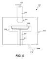
- FIG. 5is a schematic diagram showing the basic features of a RVD reactor module suitable for practicing the current invention.
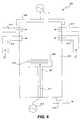
- FIG. 6is a schematic diagram showing the basic features of a HDP reactor module suitable for practicing the current invention.
- FIG. 7is a plot showing the effect of film thickness on the efficiency of the densification (anneal) process, demonstrating the effectiveness of the present invention.
- the present inventionprovides a multi-step method of forming a densified silicon oxide-based dielectric film.
- a thin layer of silicon oxide-based dielectricis thermally deposited.
- the dielectric filmis densified by an annealing process that removes water from the deposited layer.
- the deposition and anneal stepsare then repeated until the desired dielectric film thickness is obtained.
- the techniqueenables dielectric gap fill to the 45 nm technology node and beyond, while maintaining film properties. It accomplishes the densification of the thermally deposited oxide films without the need for high temperature anneal in structures as deep as 1 um.
- the dielectric depositionmay be by any suitable thermal process, for example CVD or RVD.
- the dielectricmay be any suitable silicon oxide-based material, doped or undoped, for example undoped silicon dioxide (undoped silica glass (USG)).
- the deposited dielectric layersshould be thin enough that they are substantially completely penetrated by the annealing process agent (e.g., oxygen-based plasma, heat, radiation or associated active chemical species) and that the water (H 2 O) generated during annealing can migrate out of the layer. In this manner, efficient removal of H 2 O from the film is facilitated, since the diffusion length for H 2 O is reduced relative to conventional thicker film depositions. In general, a layer thickness of about 20-20,000 ⁇ or 100-5000 ⁇ is suitable.
- annealingmay be accomplished by a number of different techniques, including thermal, plasma and radiation based processes.
- suitable annealing processesinclude thermal, furnace based; (rapid thermal processing (RTP) or rapid thermal oxidation (RTO) based; high density plasma based; capacitive (PECVD) plasma based; laser ablation based; UV film cure based; IR film cure based; and microwave plasma based.
- RTPrapid thermal processing
- PECVDrapid thermal oxidation
- PECVDplasma based
- laser ablation basedlaser ablation based
- UV film cure basedIR film cure based
- microwave plasma basedmicrowave plasma based.
- HDPhigh density plasma
- anneal processescan be thermal based, carried out in a furnace with an oxidizing environment, or incorporate a radiation anneal (UV for example). These techniques have the advantage of annealing while staying within the thermal budget constraints of temperature sensitive dielectric formation applications, e.g., PMD.
- FIGS. 1A and Billustrate this problem of incomplete densification of the film and the improved results obtainable using the present invention.
- FIG. 1Ashows a thick oxide film 102 , e.g., greater than 3000 ⁇ of RVD silicon dioxide, deposited on a silicon substrate 104 in a single step following annealing with an HDP plasma in a single step. Since H 2 O removal during the anneal process is diffusion limited, it is easier for water to diffuse from the top of the film than the bottom.
- Wet etch rate ratio (WERR) data collected for such filmsshows a variable film density, decreasing as a function of depth.
- WERRwet etch rate ratio
- FIG. 1Bshows an oxide film 112 of the same thickness as 102 ( FIG. 1A ), e.g., greater than 3000 ⁇ of RVD silicon dioxide, on a silicon substrate 114 .
- the filmis deposited and annealed by the multi-step technique of the present invention in which thin (e.g. 1000 ⁇ ) oxide layers are deposited and annealed in series to build up the total desired film thickness.
- the annealing process agente.g., oxygen-based plasma, heat, radiation or associated active chemical species
- the filmis etched (the etch direction is shown by arrow 116 ), the amount of film etched is uniform across the thickness of the film.
- the gapis partially filled with a layer of oxide; then the oxide layer is annealed to densify the oxide layer. These steps are repeated until the gap is filled with a significantly densified oxide film.
- the post-deposition annealing treatment stepcan be carried out in situ in the deposition chamber, in an integrated mode (tool), or in a separate chamber (with vacuum break). It can be carried out in an oxidizing or inert ambient (e.g., N 2 ) environment.
- an oxidizing or inert ambiente.g., N 2
- the use of water vapor as an ambient gas for the post-deposition anneal processing of oxide-based filmis a known technique.
- the anneal stepis followed by a second deposition step and the cycle is repeated until the desired densified film thickness is achieved, e.g., the structure is fully filled and densified.
- FIG. 2provides a flow illustration of a process in accordance with the present invention.
- a thin oxide layeris deposited on a substrate, for example by exposing the substrate surface to a silicon-containing precursor gas to form a silicon oxide-based dielectric film layer on the substrate ( 201 ). If the dielectric is deposited over a substrate feature such as a gap, the thin layer only partially fills the gap. In general, the layer is sufficiently thin to not prevent substantially complete penetration of the annealing agent into the layer and migration of water out of the layer.
- the thin layeris then annealed to remove water ( 203 ), and the deposition and anneal steps are repeated at least once to form a densified dielectric film of a desired thickness, e.g., a film that fills a gap ( 205 ).
- FIGS. 3A and BThe relative improvement in performance achieved by the method of the present invention in a gap fill application is illustrated in FIGS. 3A and B.
- FIG. 3Arepresents a single step RVD oxide deposition and anneal process. Decoration of such a sample (e.g., by 6:1 BOE for 10 sec) dissolves low density (only partially densified) oxide material and creates voids 301 in the trench.
- FIG. 3Brepresents a multi-step process in accordance with the invention, each cycle a RVD thin oxide deposition followed by anneal. Since the film is fully densified, no material is dissolved by decoration of such a sample in the same way. Hence, the film's performance is improved. For example in post-STI processing (such as wet dips) the film will be better at preventing any void or open seam formation.
- post-STI processingsuch as wet dips
- a preferred annealing processis high density plasma (HDP)-based.
- HDPhigh density plasma
- a high density plasma in an oxidizing environmentcan fully and uniformly densify thin dielectric films at low temperatures. This technique has the advantage of annealing while staying within the thermal budget constraints of temperature sensitive dielectric formation applications, e.g., PMD.
- a RVD methodinvolves sequentially depositing a plurality of atomic-scale films on a substrate surface by sequentially exposing and removing reactants to and from the substrate surface.
- An exemplary case of RVD using reactant gases A and Bwill now be used to illustrate principle operations of a RVD process in accordance with the present invention.
- gas Ais injected into a chamber and the molecules of gas A are chemically or physically adsorbed to the surface of a substrate, thereby forming a “saturated layer” of A.
- Formation of a saturated layeris self-limiting in nature and represents a thermodynamically distinct state of adsorbed A on a surface. In some cases, a saturated layer is only one monolayer. In other cases, a saturated layer is a fraction of a monolayer, or some multiple of monolayers.
- the remaining gas A in the chamberis purged using an inert gas.
- the gas Bis injected so that it comes in contact with the adsorbed layer of A and reacts to form a reaction product of A and B. Because the saturated layer of A is nominally thin and evenly distributed over the substrate surface, excellent film step coverage can be obtained.
- Bis flowed over the substrate for a period of time sufficient to allow the reaction between A and B to preferably go to completion; i.e., all of the adsorbed A is consumed in the reaction.
- Bis flowed over the substrate for a period of time sufficient for B to accumulate to thicknesses in excess of one monolayer.
- RVD methodsare related to the well-established chemical vapor deposition (CVD) techniques; both are thermal deposition techniques.
- CVDchemical vapor deposition
- the chemical reactant gasesare simultaneously introduced in a reaction chamber and allowed to mix and chemically react with each other in gas phase. The products of the mixed gases are then deposited on the substrate surface.
- RVD methodsdiffer from CVD since in RVD the chemical reactant gases are individually injected into a reaction chamber and not allowed to mix prior to contacting the substrate surface. That is, RVD is based on separated surface-controlled reactions. Either RVD, CVD, or spin-on glass deposition may be used for film deposition in accordance with the present invention.
- FIG. 4is a process flow diagram illustrating relevant operations in a multi-step rapid vapor deposition (RVD) and high-density plasma (HDP) anneal process to form a fully densified dielectric film in accordance with one embodiment of the present invention.
- RVDrapid vapor deposition
- HDPhigh-density plasma
- the deposition process 400begins with operation 401 , wherein a substrate is placed into a deposition chamber.
- the substrateis a semiconductor wafer.
- a “semiconductor wafer” as discussed in this documentis a semiconductor substrate at any of the various states of manufacture/fabrication in the production of integrated circuits.
- PMDpremetal dielectric
- STIshallow trench isolation
- an RVD processis used to deposit a dielectric layer on the substrate.
- a suitable RVD processsee U.S. patent application Ser. No. 10/672,309, titled “Properties of a Silica Thin Film Produced by a Rapid Vapor Deposition [RVD] Process”, filed on Sep. 26, 2003, which is incorporated by reference herein for all purposes.
- a catalyst or catalyst-containing precursor gasis pumped into the deposition chamber so as to substantially saturate the surface with the catalyst or catalyst-containing precursor.
- any suitable catalyst or catalyst-containing precursor that can sufficiently adsorb onto the substrate surface and sufficiently react with the subsequently added silicon-containing precursor to form a dielectric layer that is more than a monolayer thickmay be used.
- the catalyst or catalyst-containing precursorshould be capable of aiding the catalytic polymerization of the subsequently added silicon-containing precursor to produce a film thicker than a monolayer.
- an aluminum-containing precursorfor example, hexakis(dimethylamino)aluminum (Al 2 (N(CH 3 ) 2 ) 6 ) or trimethylaluminum (Al(CH 3 ) 3 ) is used.
- suitable aluminum-containing precursorsinclude, for example, triethylaluminum (Al(CH 2 CH 3 ) 3 ) or aluminum trichloride (AlCl 3 ).
- metal-containing precursors that can be deposited to reactivate the catalytic surfaceinclude, but are not limited to, zirconium, hafnium, gallium, titanium, niobium, tantalum, and their oxides or nitrides, or combinations thereof.
- forming a saturated layeris a self-limiting process and to a certain extent independent of process conditions.
- Relevant process conditionscan include pressure, precursor flow rate, substrate temperature, and dose.
- pressurescan range broadly, e.g., between about 1 mTorr and 760 Torr. Typical pressures range between about 10 mTorr and 5 Torr and typical temperatures range between about 20 and 300 degrees Celsius.
- Flow rates of aluminum-containing precursor gasfor example, can range broadly, e.g., between about 1 and 10000 sccm. Preferred flow rates of aluminum-containing precursor gas range between about 10 and 1000 sccm.
- the dose of aluminum-containing precursorcan range broadly, e.g., between about 0.001 milligrams and 10 grams. Typical aluminum-containing precursor doses range between about 0.01 and 0.1 grams. Exposure times suitable for forming a saturated layer are typically only seconds. In some embodiments, for example, an exposure time of about 1 to 2 seconds is found to be sufficient.
- silica films by a RVDcan also alternatively be catalyzed by metal and metalloid-free compounds, such as acidic compounds, for example phosphoric acid (H 3 PO 4 ).
- Metal- and metalloid-free compounds suitable as catalysts in a RVD processinclude organic acids (e.g., acetic acid), anhydrides of organic acids, dialkylphosphates, alkysphosphates, phosphonic acids, phosphinic acids, phosphorus oxides, alkylamines (primary, secondary or tertiary), arylamines, alky/arylboronic acids, sulphonic acids, water, ammonium salts, phosphonitrile compounds, boron triflates, inorganic acids (e.g., phosphoric acid), anhydrides of inorganic acids, and combinations thereof.
- organic acidse.g., acetic acid
- anhydrides of organic acidsdialkylphosphates, alkysphosphates, phosphonic acids, phosphin
- pressurescan range broadly, e.g., between about 1 mTorr and 760 Torr. Typical pressures range between about 500 and 1250 mTorr and typical temperatures range between about 0 and 300° C., for example between about 20 and 250° C., such as 20, 50, 100, 200, 230 or 250° C. in various implementations.
- Flow rates of catalyst reactantscan range broadly, e.g., between about 1 and 10000 sccm in the gas phase.
- Preferred gas phase flow rates of the catalystrange between about 1 and 1000 sccm.
- Catalystsmay also alternatively be delivered to the reactor and/or the substrate surface in the liquid phase.
- Suitable liquid phase delivery flow ratescan be between 0.01 and 100 mL/min; or the liquid catalysts can be delivered to the substrate surface by dipping, painting, spraying, etc.
- Suitable liquid phase catalyst concentrationscan vary widely, for example from about 10 ⁇ 3 to 12M, such as about 0.01, 0.1, 1, 2, 5, 7 or 10M.
- Exposure times suitable for forming a saturated layerare typically only seconds, e.g., about 0.1 to 10 seconds. In some embodiments, for example, an exposure time of about 1 seconds or 5 seconds is found to be sufficient. Given the directions and parameters provided herein, one of skill in the art will be able to readily determine the appropriate conditions for effective use of a given catalyst in accordance with the present invention.
- an inert gasis preferably used to purge the substrate surface and reaction chamber (not shown). It should be noted that introduction of a purge gas can be used in between operations wherein contact between reactant gases should be avoided, including between each process cycle. Further, the purge gas can be flowed continuously during any of these operations and a period or periods between the operations. Purge gases are generally inert. Examples include the noble gases (e.g., argon) and nitrogen.
- the reaction chambermay additionally be evacuated following inert gas purge.
- process 400continues with the exposure of the catalyst-activated substrate surface to a silicon-containing precursor gas under conditions suitable for the growth of a dielectric film in operation 405 .
- a silicon-containing precursor gasunder conditions suitable for the growth of a dielectric film in operation 405 .
- Any suitable silicon-containing precursor that can sufficiently adsorb onto and react with the saturated layer of aluminum-containing precursor to form a dielectric filmmay be used.
- the silicon-containing precursorshould be capable of polymerization when exposed to the adsorbed catalyst to produce a film thicker than a monolayer.
- Preferred silicon-containing precursorsinclude silanols and silanediols, such as alkoxysilanols, alkyl alkoxysilanols, alkyl alkoxysilanediols and alkoxysilanediols.
- suitable precursorsinclude tris(tert-butoxy)silanol ((C 4 H 9 O) 3 SiOH), tris(tert-pentoxy)silanol((C 5 H 11 O) 3 SiOH), di(tert-butoxy)silandiol ((C 4 H 9 O) 2 Si(OH) 2 ) and methyl di(tert-pentoxy)silanol.
- the catalystis adsorbed onto or reacts with the substrate surface, and the accumulation of dielectric film is achieved via a polymerization process.
- the activated substrate surface layercan catalytically polymerize the silicon-containing precursor to produce growing chains of silica. After a period of growth determined by the substrate temperature, the silica polymer can “gel” or “cross-link” to form a solid silicon dioxide.
- the final film thicknessdepends on the silicon dioxide layer formation rate and the amount of time the silicon containing precursor is exposed to the activated substrate surface layer.
- the filmcan also be made thicker by repeating the number of precursor deposition cycles.
- Process parameters during exposure to the silicon-containing precursorincluding temperature, gas pressure, flow rate, dose and exposure times will vary depending on the types of precursors used, reaction chamber configuration and desired final film thickness, deposition rate and dielectric characteristics, among other variables.
- Temperaturescan range from about 20 to 300° C.
- a typical deposition temperatureis about 20-250° C.
- Pressurescan range broadly, e.g., between about 1 mTorr and 760 Ton. Typical pressures range between about 10 mTorr and 750 5 Ton.
- Flow rates of silicon-containing precursor gascan range broadly, e.g., between about 1 and 10000 sccm.
- Preferred flow rates of silicon-containing precursor gasrange between about 10 and 1000 sccm.
- the dose of silicon-containing precursorcan range broadly, e.g., between about 0.001 milligrams and 100 grams. Typical silicon-containing precursor doses range between about 0.1 and 2 grams. Exposure times can range broadly, e.g., between about 1 milliseconds and 1000 seconds. Preferred exposure times typically range between about 1 and 100 seconds.
- the deposited dielectric layershould be thin enough that it can be substantially completely penetrated by the annealing process agent (e.g., Oxygen-based plasma, heat, radiation or associated active chemical species) in the subsequent annealing process and that the water (H 2 O) generated during annealing can migrate out of the layer.
- the annealing process agente.g., Oxygen-based plasma, heat, radiation or associated active chemical species
- H 2 Owater
- a layer thickness of about 20-20000 A, for example about 100-5000 ⁇is suitable.
- This layermay be generated in one or more depositions as described above; i.e., the RVD dielectric deposition operations 403 - 405 may be conducted once or repeated multiple times to form the layer.
- an anneal operation 407 using a low temperature oxygen-containing inductively coupled high density plasma (HDP)is performed in order to improve the mechanical properties of the film.
- the HDP annealis used to remove water from the as-deposited film.
- HDP operation 407is performed in an oxidizing environment.
- the oxidizer usedis an oxygen-containing oxidizer such as O 2 , H 2 O, H 2 O 2 , air, or O 3 .
- One advantage of using an oxygen-containing oxidizeris that the oxygen in the plasma reacts with the RVD deposited film to cross-link the silica and reduce or eliminate seams created during RVD gap fills.
- the oxygensubstitutes for the water that is removed from the film in the anneal process so that the film does not shrink and the film stress is not increased by water removal.
- STIgap fill
- HF-basedpost gap fill wet etch
- Suitable temperaturesrange from about 250° C. to 750° C.; suitable pressures range from about 1 to 1000 mTorr; and suitable time ranges from about 30 sec to 20 min.
- the annealing operationlasts from between about 330 to 700 seconds. In a second embodiment, the annealing operation lasts about 600 seconds.
- Operations 403 - 407are repeated as necessary until a desired thickness of dielectric material has been reached, e.g., a gap has been filled.
- the resulting dielectric filmhas improved properties after annealing.
- the dielectric filmmay have a k-value of between about 3.8-4.0, a film stress of between about 2 Gdyn/cm 2 tensile and 2 Gdyn/cm 2 compressive, and a wet etch rate ratio (WERR) of less than 1.3:1 relative to conventionally formed thermal oxide.
- WERRwet etch rate ratio
- This methodapplies to the deposition of silica (USG).
- this methodmay also be used for depositing doped silica films, such as fluorine-doped silicate glass (FSG), phosphosilicate glass (PSG), boro-phospho-silicate glass (BPSG), or carbon doped low-k materials.
- FSGfluorine-doped silicate glass
- PSGphosphosilicate glass
- BPSGboro-phospho-silicate glass
- carbon doped low-k materialssuch as carbon doped low-k materials.
- deposition co-reactantssuch as silanols with varying substituents (i.e., more than one kind of alkoxy substituent) may be used to improve the film characteristics.
- substituentsi.e., more than one kind of alkoxy substituent
- the properties of the dielectric filmmay be improved by other means as well, including by using an aluminum oxide nucleation layer formed by ALD prior to the application of the silica layer. See, for example, U.S. patent application Ser. No. 10/875,158, filed Jun.
- the methodis primarily described above with reference to a RVD-based embodiment, however it is also applicable to any deposition technique that forms films requiring densification, in particular CVD films.
- annealingmay be accomplished by a number of different techniques other than the HDP/O 2 anneal exemplified above, including those described below:
- Thermal, furnace basedFor example, furnace anneal at a temperature of greater than 700° C. for at least 30 minutes.
- Rapid thermal annealor rapid thermal oxidation (RTO) based: For example, anneal at a temperature of greater than 600° C. for at least 5 minutes in either inert (e.g., N 2 ) or oxidizing (e.g., 70% N 2 , 30% steam) environments, respectively).
- inerte.g., N 2
- oxidizinge.g., 70% N 2 , 30% steam
- Capacitive (PECVD) plasma basedFor example, anneal at a source power (HF) of at least 5000 W at a temperature of about 400° C. for at least 10 minutes.
- HFsource power
- Microwave plasma basedFor example, anneal at a temperature of about 200 to 400° C., a pressure of about 1 to 100 Torr, an oxygen-containing gas flow of about 2 L/min, and a power of up to 10,000 W, for at least 3 minutes.
- Laser basedFor example, application of a localized energy pulse, such as a laser pulse, for example one of about 10 to 100 ns in duration from an excimer laser, that raises the temperature of the film above 1000° C. without raising the substrate temperature sufficiently to modify its properties (e.g., the substrate temperature remains below 550° C. or preferably in many applications below 400° C.).
- a localized energy pulsesuch as a laser pulse, for example one of about 10 to 100 ns in duration from an excimer laser, that raises the temperature of the film above 1000° C. without raising the substrate temperature sufficiently to modify its properties (e.g., the substrate temperature remains below 550° C. or preferably in many applications below 400° C.).
- a localized energy pulse techniqueas described in further detail in commonly assigned co-pending application Ser. No. 11/327,668, incorporated herein by reference, can raise the temperature the film sufficiently to melt the film and/or remove hydroxyl moieties from the film.
- UV cure basedFor example, anneal at a power density of less than 5 W/cm 2 , in either inert (e.g., He, Ar, forming gas, or N 2 ) or oxidizing environments (e.g., in an anneal environment that comprises one or more of oxygen, ozone, peroxide or nitrous oxide) In oxidizing environments, oxygen can promote bond breaking thereby facilitating hydrogen removal for film densification.
- the UV sourcecan be a single wavelength excimer lamp or broad spectra source with arc or microwave excitations. The wavelength can be from about 100 nm-1000 nm, preferably from about 150-500 nm.
- the process pressurecan range from about 1 mTorr to 760 Torr, preferably from about 1 Torr to 200 Ton.
- the UV exposurecan also be achieved through direct exposure to a plasma of He, Ar, N 2 , NH 3 , N 2 O, O 2 , or a mixture of them.
- the wafer temperaturecan be set at from about 25° C. to 700° C., preferably from about 300-700° C.
- IR-based cureFor example, anneal in either inert (e.g., He, Ar, or N 2 ) or oxidizing environments with an IR source such as halogen lamps or other IR radiators can be placed directly above the substrate or through an IR-transparent window.
- the process pressurecan range from about 10 mTorr to 760 Ton, and preferably from about 1 Torr to 200 Ton.
- the wafer temperaturecan be set at 25 C to 700 C, preferably from 300-700 C.
- the electron energycan range from about 100 eV to 100 keV, preferably from about 5 keV to 30 keV for curing a film ranging from about 200 ⁇ to 2 microns.
- the process pressurecan range from about 0.001 mTorr to 760 Torr depending on the type of electron source employed.
- the wafer temperaturecan be set at about 25° C.
- the plasmamay comprise an oxygen-containing gas or forming gas (a mixture of hydrogen and nitrogen), for example.
- the down stream plasmaprovides the active molecular species to extract —OH from the film, causing effective removal of H 2 O from the film.
- the process pressurecan range from about 1 mTorr to 100 Torr, preferably from about 0.1 Torr to 10 Torr.
- the wafer temperaturecan be set at about 25° C. to 700° C., preferably from about 300-700° C.
- a plurality of layers of a multi-laminate dielectric filmmay be deposited prior to an anneal operation, as described, and then annealed in a single anneal operation, so long as the aggregate thickness of the dielectric multi-laminate film or portion thereof formed prior to annealing is insufficient to prevent substantially complete penetration of the annealing agent into the film and migration of water out of the film.
- deposition and post-deposition annealing treatment stepscan be carried out in situ in the same chamber, in an integrated mode (tool), or in separate chambers (with vacuum break).
- FIG. 5is a block diagram depicting some components of a suitable reactor for performing dielectric deposition using a RVD process in accordance with one embodiment of this invention. Note that this apparatus is only an example of suitable apparatus for deposition in accordance with this embodiment of the present invention. Many other apparatuses and systems, including a multi-chambered apparatus, may be used.
- a reactor 501includes a process chamber 503 , which encloses components of the reactor and serves to contain the reactant gases and provide and area to introduce the reactant gases to substrate 509 .
- the chamber wallsmay be made of or plated with any suitable material, generally a metal that is compatible with the deposition and associated processes conducted therein. In one example, the process chamber walls are made from aluminum.
- a wafer pedestal 507supports a substrate 509 .
- the pedestal 507typically includes a chuck 508 to hold the substrate in place during the deposition reaction.
- the chuck 508may be an electrostatic chuck, a mechanical chuck or various other types of chuck as are available for use in the industry and/or research.
- a heat transfer subsystem including lines 511 for supplying a heat transfer fluid to the pedestal 507controls the temperature of pedestal 507 .
- the heat transfer fluidcomprises water or another liquid.
- the reactant gases, as well as inert gases during purge,are introduced individually into the reactor at tube 525 via inlet 517 .
- a showerhead 527may be used to distribute the gas flow uniformly in the process reactor.
- Reactant gasesare introduced through a gas supply inlet mechanism including orifices. There may be multiple reactant gas tubes and inlets.
- a vacuum pump) connected to outlet 519can draw out gases between RVD cycles.
- FIG. 6is a block diagram depicting some components of a suitable HDP reactor for performing HDP/O 2 annealing in accordance with one embodiment of this invention. Note that this apparatus is only an example of suitable apparatus for annealing in accordance with this embodiment of the present invention. Many other apparatuses and systems, including a multi-chambered apparatus, may be used.
- Suitable reactorsinclude a reaction chamber, a process gas delivery system, a support for the substrate, one or more electrodes to generate a plasma and a bias source for the substrate.
- the particular designis not critical to this invention. It merely needs to support an inductively coupled high-density plasma generated by the appropriate gases over the appropriate substrates.
- suitable reactorsinclude the Novellus SPEED reactor, available from Novellus Systems, Inc. of San Jose, Calif., and the Ultima reactor, available from Applied Materials, Inc. of Santa Clara, Calif.
- a reactor 601includes a process chamber 603 which encloses other components of the reactor and serves to contain the plasma generated by an electrode 605 .
- the process chamber wallsare made from aluminum, aluminum oxide, and/or other suitable material.
- Electrode 605is powered by a “low frequency” RF source 606 . The power and frequency supplied by source 606 is sufficient to generate high-density plasma from the process gas.
- a wafer pedestal 607supports a substrate 609 .
- the pedestaltypically includes a chuck to hold the substrate in place during the deposition reaction.
- the chuckmay be an electrostatic chuck, a mechanical chuck or various other types of chuck as are available for use in the industry and/or research.
- a heat transfer subsystem including a line 611 for supplying a heat transfer fluidcontrols the temperature of substrate 609 .
- the heat transfer fluidcomprises at least one of helium and argon gas.
- the heat transfer fluidis supplied to a space 613 between the surface of the substrate and a surface of the chuck.
- a “high frequency” RF source 615serves to electrically bias substrate 609 and draw charged precursor species onto the substrate for the deposition reaction. Electrical energy from source 615 is coupled to substrate 609 via an electrode or capacitive coupling, for example. Note that the bias applied to the substrate need not be an RF bias. Other frequencies and DC bias may be used as well. In a specific embodiment, source 615 supplies a radio frequency bias to the substrate, and the radio frequency bias is generated by supplying the electrode with about 500 W of power.
- the process gasesfor example oxidant (e.g., O 2 ), are introduced via one or more inlets 617 and 617 ′.
- the gasesmay be premixed or not.
- the process gasis introduced through a gas supply inlet mechanism including orifices.
- at least some of the orificesorient the process gas along an axis of injection intersecting an exposed surface of the substrate at an acute angle.
- the gases or gas mixturesmay be introduced from a primary gas ring, which may or may not direct the gases toward the substrate surface.
- Injectorsmay be connected to the primary gas ring to direct at least some of the gases or gas mixtures into the chamber and toward substrate.
- injectors, gas rings or other mechanisms for directing process gas toward the waferare not critical to this invention.
- the sonic front caused by a process gas entering the chamberwill itself cause the gas to rapidly disperse in all directions—including toward the substrate.
- Process gasesexit chamber 603 via an outlet 619 .
- a vacuum pumpe.g., a turbomolecular pump typically draws process gases out and maintains a suitably low pressure within the reactor.
- Reactor pressureis held at a value necessary to sustain the high-density plasma.
- the process vesselis maintained at a pressure of at most about 200 mTorr.
- the process chamber pressureis maintained below 1 mTorr.
- the pressureis maintained between about 1 and 1000 mTorr; most preferably between about 1 and 30 mTorr. In one embodiment of the invention, the pressure is maintained at about 2 mTorr during annealing.
- Wafer temperatureshould be maintained sufficiently high to ensure that complete film densification.
- the temperaturemay be limited by process constraints, such as thermal budget limitations that preclude temperatures above 500° C. Such constraints become increasingly common with advanced technologies and corresponding smaller feature sizes.
- the anneal temperatureis preferably maintained between about 300 and 500° C.
- the low frequency power applied to the upper electrode (for generating the plasma)typically varies from 1 kW to 20 kW, and the high frequency power (for biasing the wafer) typically reaches at least about 0.1 W/cm 2 , for example 1W/cm 2 (preferably varying from about 0.5 kW to 10 kW) depending on the substrate size (e.g., 200 or 300 mm diameter) and the requirements of the specific process being used.
- the bias applied to the substrateis typically a radio frequency bias. Applying radio frequency bias to the substrate involves supporting the substrate on a substrate holder having an electrode supplying a radio frequency bias to the substrate.
- the radio frequency bias applied to the substrateis at the frequency range of between about 100 kHz and 27 MHz.
- the frequency range applied to the upper, plasma-generating electrodeis typically between about 300 kHz and 27 MHz.
- FIG. 7shows the effect of film thickness on the efficiency of the densification (annealing) process.
- SiO 2 filmswere deposited by RVD using a silicon precursor partial pressure below 10 Torr and a temperature of 230° C. Films were annealed by RTP at the temperatures indicated for at least 5 minutes at ambient pressure in a mixture of 30% steam and 70% N 2 .
- the films' wet etch ratewhich is a measure of film density, was measured at the top and at the bottom of the stack. For the 5000 ⁇ films, the difference is in the order of 40%, while for films 2000 ⁇ thick the wet etch rate measurements were within 12% at temperatures above 700° C. This result indicates that the thinner films were more efficiently and uniformly densified from top to bottom.
Landscapes
- Engineering & Computer Science (AREA)
- Physics & Mathematics (AREA)
- Microelectronics & Electronic Packaging (AREA)
- Condensed Matter Physics & Semiconductors (AREA)
- General Physics & Mathematics (AREA)
- Manufacturing & Machinery (AREA)
- Computer Hardware Design (AREA)
- Power Engineering (AREA)
- Toxicology (AREA)
- Optics & Photonics (AREA)
- Health & Medical Sciences (AREA)
- Plasma & Fusion (AREA)
- Chemical & Material Sciences (AREA)
- Chemical Kinetics & Catalysis (AREA)
- Formation Of Insulating Films (AREA)
Abstract
Description
This application is a continuation-in-part of U.S. patent application Ser. No. 10/975,028 filed Oct. 26, 2004 now U.S. Pat. No. 7,148,155, titled SEQUENTIAL DEPOSITION /ANNEAL FILM DENSIFICATION METHOD , incorporated herein by reference in its entirety for all purposes.
The present invention relates to the formation of dielectric films, in particular to the formation of dense dielectric films in high aspect ratio features on semiconductor substrates.
It is often necessary in semiconductor processing to fill a high aspect ratio gap with insulating material. One example of a high aspect ratio trench encountered in semi-conductor processing is in the formation of shallow trench isolation (STI). As device dimensions shrink and thermal budgets are reduced, void-free filling of high aspect ratio spaces (AR>3.0:1) becomes increasingly difficult due to limitations of existing deposition processes. The deposition of doped or undoped silicon dioxide assisted by high density plasma CVD, a directional (bottom-up) CVD process, is the method currently used for high aspect ratio (AR) gap-fill. Evolving semiconductor device designs and dramatically reduced feature sizes have resulted in several applications where HDP processes are challenged in filling the high aspect ratio structures (AR>7:1) using existing technology (see, for example, U.S. Pat. No. 6,030,881). For structures representative of the 65 nm and 45 nm technology nodes, engineering the gap-fill process becomes structure dependent, hence the process needs to be reoptimized, a task of considerable complexity, every time a new structure needs to be filled.
An alternative to CVD is atomic layer deposition (ALD). ALD methods involve self-limiting adsorption of reactant gases and can provide thin, conformal dielectric films within high aspect ratio features. An ALD-based dielectric deposition technique typically involves adsorbing a metal containing precursor onto the substrate surface, then, in a second procedure, introducing a silicon oxide precursor gas. The silicon oxide precursor gas reacts with the adsorbed metal precursor to form a thin film of metal-doped silicon oxide. One drawback, however, to ALD is that the deposition rates are very low. Films produced by ALD are also very thin (i.e., about one monolayer); therefore, numerous ALD cycles must be repeated to adequately fill a gap feature. These processes are unacceptably slow in some applications in the manufacturing environment.
A related technique, referred to as rapid vapor deposition (RVD) or pulsed deposition layer (PDL) processing, is another alternative. RVD is similar to ALD in that reactant gases are introduced alternately over the substrate surface, but in RVD the silicon oxide film can grow more thickly. Thus, RVD methods allow for rapid film growth similar to using CVD methods but with the film conformality of ALD methods. An example of the process is described in the paper by Hausmann et. al. entitled Rapid Vapor Deposition of Highly Conformal Silica Nanolaminates (2002, Science, 298, pages 403-406).
Deposited oxide films require densification in order for its properties to match those of thermally generated silicon oxide (USG, which will allow its successful integration into functioning devices. Densification removes water from the deposited film. Moreover, the conformal nature of the process results in the formation of seams in filled trenches, which may allow attack by post gap fill wet etch (HF-based) in the seam. Etching in the seam can allow for polysilicon deposition in the seam during subsequent processing which would obviate its insulating effect. Therefore, a process sequence to anneal the film and substantially eliminate seams and voids is required.
Optimally, this process sequence can operate at under 500° C., in order to be able to meet the thermal budget requirements of advanced devices (see A. R. Londergan, et. al., J. Electrochem. Soc., vol. 148, pp. C21-C27, January 2001). In premetal dielectric (PMD) applications, for example, where a layer of silica is applied over gates that have been previously built-up on a substrate, there is an inherent temperature limitation due to the material used to construct the gates, usually a metal silicide such as a nickel silicide. At temperatures above about 400-500° C., the gate silicide may become discontinuous, thereby increasing the resistance of the circuit and leading to performance problems. Further, there may be two or three PMD layers applied to a substrate before application of metal conductors. Thus, it is desirable to implement a method to improve the material properties of the dielectric film, ideally maintaining temperatures that are low enough to avoid damaging underlying heat sensitive structures.
The present invention addresses this need by providing a multi-step method of forming a densified silicon oxide-based dielectric film. First, a thin layer of silicon oxide-based dielectric is thermally deposited. Then, the dielectric film is densified by an annealing process that removes water from the deposited layer. The deposition and anneal steps are then repeated until the desired dielectric film thickness is obtained. The technique enables dielectric gap fill to the 45 nm technology node and beyond, while maintaining film properties. It accomplishes the densification of the thermally deposited oxide films without the need for high temperature anneal in structures as deep as 1 um.
The dielectric deposition may be by any suitable process, for example CVD, SOG (spin-on glass), or RVD. The dielectric may be any suitable silicon oxide-based material, doped or undoped, for example undoped silicon dioxide (undoped silica glass (USG)). The deposited dielectric layers should be thin enough that they are substantially completely penetrated by the annealing process agent (e.g., Oxygen-based plasma, heat, radiation or associated active chemical species) and that the water (H2O) generated during annealing can migrate out of the layer. In this manner, efficient removal of H2O from the film is facilitated, since the diffusion length for H2O is reduced relative to conventional thicker film depositions. In general, a layer thickness of about 300-3000 Å or 500-1500 Å, for example about 1000 Å is suitable.
Annealing may be accomplished by a number of different techniques, including thermal, plasma and radiation based processes. A preferred annealing process is high density plasma (HDP)-based. A high density plasma in an oxidizing environment can densify thin dielectric films at low temperatures. Thus, this technique has the advantage of annealing while staying within the thermal budget constraints of temperature sensitive dielectric formation applications, e.g., PMD.
In one embodiment, silica nanolaminates formed in a high aspect ratio feature by rapid vapor deposition (RVD) are annealed in a HDP reactor in order to densify the layers and eliminate seams and voids, which are caused by the conformal nature of RVD. This method involves the following principle operations: 1) exposing a substrate surface to a catalytic metal-containing precursor gas to form a substantially saturated layer of catalytic metal-containing precursor on the substrate surface, 2) exposing the substrate surface to a silicon-containing precursor gas to form a thin dielectric layer on the substrate surface, 3) annealing the thin layer at a temperature below 500° C. using HDP under oxidizing conditions; and 4) repeating1) to 3) until a desired dielectric film thickness is achieved, e.g., until the gap is filled. The O2based HDP reactive plasma results in film densification and cross-linking at temperatures of less than 500° C. Low temperature operation is enabled by the high concentration of reactive species in the high density plasma. The film expands as a result of Si—O bond formation during annealing, eliminating seams in the film, a critical element for its successful integration. Optimizing film properties at low temperature allows for the use of the film low thermal budget PMD applications.
The method of the invention can be used for forming a dielectric film for any purpose. In a specific embodiment, it is used for filling structures, such as gaps, in particular high aspect ratio trenches, on semiconductor substrates, e.g., IMD, PMD and STI applications.
Various RVD process precursors may be used in preferred embodiments of the invention. For example, a catalytic metal-containing precursor can be an aluminum-containing precursor, such as hexakis(dimethylamino) aluminum or trimethyl aluminum. The formation of silica films by RVD can also alternatively be catalyzed by metal and metalloid-free compounds, such as acidic compounds, for example phosphoric acid (H3PO4).
The silicon containing precursor can be a silanol, such as tris(tert-butoxy)silanol ((C4H9O)3SiOH) or tris(tert-pentoxy)silanol ((C5H11O)3SiOH), or a silanediol, such as di(tert-butoxy)silandiol. Preferred flow rates for the silicon-containing precursor range between about 20 to 1000 sccm.
The resulting dielectric film has improved properties after annealing. For example, the dielectric film may have a k-value of between about 3.8-4.3, a film stress of between about 2 Gdyn/cm2tensile and 2 Gdyn/cm2compressive, and a wet etch rate ratio (WERR) of less than 1.3:1 relative to conventionally formed thermal oxide.
Exposure to the aluminum-containing precursor and the silicon-containing precursor may occur in the same chamber or different chambers in preferred embodiments of the invention. Further, additional precursor gases may be used.
These and other aspects and advantages of the present invention are described below.
Reference will now be made in detail to specific embodiments of the invention. Examples of the specific embodiments are illustrated in the accompanying drawings. While the invention will be described in conjunction with these specific embodiments, it will be understood that it is not intended to limit the invention to such specific embodiments. On the contrary, it is intended to cover alternatives, modifications, and equivalents as may be included within the spirit and scope of the invention as defined by the appended claims. In the following description, numerous specific details are set forth in order to provide a thorough understanding of the present invention. The present invention may be practiced without some or all of these specific details. In other instances, well known process operations have not been described in detail in order not to unnecessarily obscure the present invention.
As indicated, the present invention provides a multi-step method of forming a densified silicon oxide-based dielectric film. First, a thin layer of silicon oxide-based dielectric is thermally deposited. Then, the dielectric film is densified by an annealing process that removes water from the deposited layer. The deposition and anneal steps are then repeated until the desired dielectric film thickness is obtained. The technique enables dielectric gap fill to the 45 nm technology node and beyond, while maintaining film properties. It accomplishes the densification of the thermally deposited oxide films without the need for high temperature anneal in structures as deep as 1 um.
General Process Parameters
The dielectric deposition may be by any suitable thermal process, for example CVD or RVD. The dielectric may be any suitable silicon oxide-based material, doped or undoped, for example undoped silicon dioxide (undoped silica glass (USG)). The deposited dielectric layers should be thin enough that they are substantially completely penetrated by the annealing process agent (e.g., oxygen-based plasma, heat, radiation or associated active chemical species) and that the water (H2O) generated during annealing can migrate out of the layer. In this manner, efficient removal of H2O from the film is facilitated, since the diffusion length for H2O is reduced relative to conventional thicker film depositions. In general, a layer thickness of about 20-20,000 Å or 100-5000 Å is suitable.
As described further below, annealing may be accomplished by a number of different techniques, including thermal, plasma and radiation based processes. Specific examples of suitable annealing processes include thermal, furnace based; (rapid thermal processing (RTP) or rapid thermal oxidation (RTO) based; high density plasma based; capacitive (PECVD) plasma based; laser ablation based; UV film cure based; IR film cure based; and microwave plasma based. One suitable annealing process is high density plasma (HDP)-based. A high density plasma in an oxidizing environment can fully and uniformly densify thin dielectric films at low temperatures. Alternative anneal processes can be thermal based, carried out in a furnace with an oxidizing environment, or incorporate a radiation anneal (UV for example). These techniques have the advantage of annealing while staying within the thermal budget constraints of temperature sensitive dielectric formation applications, e.g., PMD.
The anneal process is rate limited by the diffusion of H2O through the film. Therefore, thicker films (e.g., greater than 500 nm thick) or films deposited in the deep trenches, which are encountered in STI and PMD applications, cannot be densified to a sufficient level in a single anneal step.FIGS. 1A and B illustrate this problem of incomplete densification of the film and the improved results obtainable using the present invention.
In one embodiment where the dielectric deposition is used to fill gaps, the gap is partially filled with a layer of oxide; then the oxide layer is annealed to densify the oxide layer. These steps are repeated until the gap is filled with a significantly densified oxide film.
The post-deposition annealing treatment step can be carried out in situ in the deposition chamber, in an integrated mode (tool), or in a separate chamber (with vacuum break). It can be carried out in an oxidizing or inert ambient (e.g., N2) environment. For example, the use of water vapor as an ambient gas for the post-deposition anneal processing of oxide-based film is a known technique.
The anneal step is followed by a second deposition step and the cycle is repeated until the desired densified film thickness is achieved, e.g., the structure is fully filled and densified.
The foregoing process is summarized inFIG. 2 which provides a flow illustration of a process in accordance with the present invention. A thin oxide layer is deposited on a substrate, for example by exposing the substrate surface to a silicon-containing precursor gas to form a silicon oxide-based dielectric film layer on the substrate (201). If the dielectric is deposited over a substrate feature such as a gap, the thin layer only partially fills the gap. In general, the layer is sufficiently thin to not prevent substantially complete penetration of the annealing agent into the layer and migration of water out of the layer. The thin layer is then annealed to remove water (203), and the deposition and anneal steps are repeated at least once to form a densified dielectric film of a desired thickness, e.g., a film that fills a gap (205).
The relative improvement in performance achieved by the method of the present invention in a gap fill application is illustrated inFIGS. 3A and B.FIG. 3A represents a single step RVD oxide deposition and anneal process. Decoration of such a sample (e.g., by 6:1 BOE for 10 sec) dissolves low density (only partially densified) oxide material and createsvoids 301 in the trench.FIG. 3B represents a multi-step process in accordance with the invention, each cycle a RVD thin oxide deposition followed by anneal. Since the film is fully densified, no material is dissolved by decoration of such a sample in the same way. Hence, the film's performance is improved. For example in post-STI processing (such as wet dips) the film will be better at preventing any void or open seam formation.
A preferred annealing process is high density plasma (HDP)-based. A high density plasma in an oxidizing environment can fully and uniformly densify thin dielectric films at low temperatures. This technique has the advantage of annealing while staying within the thermal budget constraints of temperature sensitive dielectric formation applications, e.g., PMD.
Generally, a RVD method involves sequentially depositing a plurality of atomic-scale films on a substrate surface by sequentially exposing and removing reactants to and from the substrate surface. An exemplary case of RVD using reactant gases A and B will now be used to illustrate principle operations of a RVD process in accordance with the present invention. First, gas A is injected into a chamber and the molecules of gas A are chemically or physically adsorbed to the surface of a substrate, thereby forming a “saturated layer” of A. Formation of a saturated layer is self-limiting in nature and represents a thermodynamically distinct state of adsorbed A on a surface. In some cases, a saturated layer is only one monolayer. In other cases, a saturated layer is a fraction of a monolayer, or some multiple of monolayers.
After a saturated layer of A is formed, typically, the remaining gas A in the chamber is purged using an inert gas. Thereafter, the gas B is injected so that it comes in contact with the adsorbed layer of A and reacts to form a reaction product of A and B. Because the saturated layer of A is nominally thin and evenly distributed over the substrate surface, excellent film step coverage can be obtained. B is flowed over the substrate for a period of time sufficient to allow the reaction between A and B to preferably go to completion; i.e., all of the adsorbed A is consumed in the reaction. In a RVD process, B is flowed over the substrate for a period of time sufficient for B to accumulate to thicknesses in excess of one monolayer. After a desired film thickness is achieved, the flow of B is stopped and the reaction is halted. At this point, residual gas B and any byproducts of the reaction are purged from the chamber. Further RVD cycles of substrate exposure to A, followed by exposure to B, can be implemented and repeated as needed for multiple layers of material to be deposited.
RVD methods are related to the well-established chemical vapor deposition (CVD) techniques; both are thermal deposition techniques. However, in CVD, the chemical reactant gases are simultaneously introduced in a reaction chamber and allowed to mix and chemically react with each other in gas phase. The products of the mixed gases are then deposited on the substrate surface. Thus, RVD methods differ from CVD since in RVD the chemical reactant gases are individually injected into a reaction chamber and not allowed to mix prior to contacting the substrate surface. That is, RVD is based on separated surface-controlled reactions. Either RVD, CVD, or spin-on glass deposition may be used for film deposition in accordance with the present invention.
Thedeposition process 400 begins withoperation 401, wherein a substrate is placed into a deposition chamber. For many embodiments of the invention, the substrate is a semiconductor wafer. A “semiconductor wafer” as discussed in this document is a semiconductor substrate at any of the various states of manufacture/fabrication in the production of integrated circuits. As mentioned previously, two commercially important applications of the present invention are premetal dielectric (PMD) and shallow trench isolation (STI).
Next, in operations403-405, an RVD process is used to deposit a dielectric layer on the substrate. For an example of a suitable RVD process, see U.S. patent application Ser. No. 10/672,309, titled “Properties of a Silica Thin Film Produced by a Rapid Vapor Deposition [RVD] Process”, filed on Sep. 26, 2003, which is incorporated by reference herein for all purposes. Inoperation 403, a catalyst or catalyst-containing precursor gas is pumped into the deposition chamber so as to substantially saturate the surface with the catalyst or catalyst-containing precursor.
Any suitable catalyst or catalyst-containing precursor that can sufficiently adsorb onto the substrate surface and sufficiently react with the subsequently added silicon-containing precursor to form a dielectric layer that is more than a monolayer thick may be used. In addition, the catalyst or catalyst-containing precursor should be capable of aiding the catalytic polymerization of the subsequently added silicon-containing precursor to produce a film thicker than a monolayer. In preferred embodiments, an aluminum-containing precursor, for example, hexakis(dimethylamino)aluminum (Al2(N(CH3)2)6) or trimethylaluminum (Al(CH3)3) is used. Other suitable aluminum-containing precursors include, for example, triethylaluminum (Al(CH2CH3)3) or aluminum trichloride (AlCl3). Other metal-containing precursors that can be deposited to reactivate the catalytic surface include, but are not limited to, zirconium, hafnium, gallium, titanium, niobium, tantalum, and their oxides or nitrides, or combinations thereof.
As indicated earlier, forming a saturated layer is a self-limiting process and to a certain extent independent of process conditions. Relevant process conditions can include pressure, precursor flow rate, substrate temperature, and dose. For a metal catalyst-containing precursor, pressures can range broadly, e.g., between about 1 mTorr and 760 Torr. Typical pressures range between about 10 mTorr and 5 Torr and typical temperatures range between about 20 and 300 degrees Celsius. Flow rates of aluminum-containing precursor gas, for example, can range broadly, e.g., between about 1 and 10000 sccm. Preferred flow rates of aluminum-containing precursor gas range between about 10 and 1000 sccm. The dose of aluminum-containing precursor, for example, can range broadly, e.g., between about 0.001 milligrams and 10 grams. Typical aluminum-containing precursor doses range between about 0.01 and 0.1 grams. Exposure times suitable for forming a saturated layer are typically only seconds. In some embodiments, for example, an exposure time of about 1 to 2 seconds is found to be sufficient.
The formation of silica films by a RVD can also alternatively be catalyzed by metal and metalloid-free compounds, such as acidic compounds, for example phosphoric acid (H3PO4). Metal- and metalloid-free compounds suitable as catalysts in a RVD process include organic acids (e.g., acetic acid), anhydrides of organic acids, dialkylphosphates, alkysphosphates, phosphonic acids, phosphinic acids, phosphorus oxides, alkylamines (primary, secondary or tertiary), arylamines, alky/arylboronic acids, sulphonic acids, water, ammonium salts, phosphonitrile compounds, boron triflates, inorganic acids (e.g., phosphoric acid), anhydrides of inorganic acids, and combinations thereof.
For a metal- and metalloid-free catalyst, pressures can range broadly, e.g., between about 1 mTorr and 760 Torr. Typical pressures range between about 500 and 1250 mTorr and typical temperatures range between about 0 and 300° C., for example between about 20 and 250° C., such as 20, 50, 100, 200, 230 or 250° C. in various implementations. Flow rates of catalyst reactants can range broadly, e.g., between about 1 and 10000 sccm in the gas phase. Preferred gas phase flow rates of the catalyst range between about 1 and 1000 sccm. Catalysts may also alternatively be delivered to the reactor and/or the substrate surface in the liquid phase. Suitable liquid phase delivery flow rates can be between 0.01 and 100 mL/min; or the liquid catalysts can be delivered to the substrate surface by dipping, painting, spraying, etc. Suitable liquid phase catalyst concentrations can vary widely, for example from about 10−3to 12M, such as about 0.01, 0.1, 1, 2, 5, 7 or 10M. Exposure times suitable for forming a saturated layer are typically only seconds, e.g., about 0.1 to 10 seconds. In some embodiments, for example, an exposure time of about 1 seconds or 5 seconds is found to be sufficient. Given the directions and parameters provided herein, one of skill in the art will be able to readily determine the appropriate conditions for effective use of a given catalyst in accordance with the present invention.
After the catalyst layer is formed an inert gas is preferably used to purge the substrate surface and reaction chamber (not shown). It should be noted that introduction of a purge gas can be used in between operations wherein contact between reactant gases should be avoided, including between each process cycle. Further, the purge gas can be flowed continuously during any of these operations and a period or periods between the operations. Purge gases are generally inert. Examples include the noble gases (e.g., argon) and nitrogen. The reaction chamber may additionally be evacuated following inert gas purge.
Next, after the chamber is purged,process 400 continues with the exposure of the catalyst-activated substrate surface to a silicon-containing precursor gas under conditions suitable for the growth of a dielectric film inoperation 405. Any suitable silicon-containing precursor that can sufficiently adsorb onto and react with the saturated layer of aluminum-containing precursor to form a dielectric film may be used. In addition, the silicon-containing precursor should be capable of polymerization when exposed to the adsorbed catalyst to produce a film thicker than a monolayer. Preferred silicon-containing precursors include silanols and silanediols, such as alkoxysilanols, alkyl alkoxysilanols, alkyl alkoxysilanediols and alkoxysilanediols. Examples of suitable precursors include tris(tert-butoxy)silanol ((C4H9O)3SiOH), tris(tert-pentoxy)silanol((C5H11O)3SiOH), di(tert-butoxy)silandiol ((C4H9O)2Si(OH)2) and methyl di(tert-pentoxy)silanol.
While the invention is not limited to this theory of operation, as mentioned previously, it is believed that the catalyst is adsorbed onto or reacts with the substrate surface, and the accumulation of dielectric film is achieved via a polymerization process. The activated substrate surface layer can catalytically polymerize the silicon-containing precursor to produce growing chains of silica. After a period of growth determined by the substrate temperature, the silica polymer can “gel” or “cross-link” to form a solid silicon dioxide. The final film thickness depends on the silicon dioxide layer formation rate and the amount of time the silicon containing precursor is exposed to the activated substrate surface layer. The film can also be made thicker by repeating the number of precursor deposition cycles.
Process parameters during exposure to the silicon-containing precursor including temperature, gas pressure, flow rate, dose and exposure times will vary depending on the types of precursors used, reaction chamber configuration and desired final film thickness, deposition rate and dielectric characteristics, among other variables. Temperatures can range from about 20 to 300° C. A typical deposition temperature is about 20-250° C. Pressures can range broadly, e.g., between about 1 mTorr and 760 Ton. Typical pressures range between about 10 mTorr and 750 5 Ton. Flow rates of silicon-containing precursor gas can range broadly, e.g., between about 1 and 10000 sccm. Preferred flow rates of silicon-containing precursor gas range between about 10 and 1000 sccm. The dose of silicon-containing precursor can range broadly, e.g., between about 0.001 milligrams and 100 grams. Typical silicon-containing precursor doses range between about 0.1 and 2 grams. Exposure times can range broadly, e.g., between about 1 milliseconds and 1000 seconds. Preferred exposure times typically range between about 1 and 100 seconds.
The deposited dielectric layer should be thin enough that it can be substantially completely penetrated by the annealing process agent (e.g., Oxygen-based plasma, heat, radiation or associated active chemical species) in the subsequent annealing process and that the water (H2O) generated during annealing can migrate out of the layer. In general, a layer thickness of about 20-20000 A, for example about 100-5000 Å is suitable. This layer may be generated in one or more depositions as described above; i.e., the RVD dielectric deposition operations403-405 may be conducted once or repeated multiple times to form the layer.
Returning toFIG. 4 , after a thin dielectric layer has been formed, ananneal operation 407 using a low temperature oxygen-containing inductively coupled high density plasma (HDP) is performed in order to improve the mechanical properties of the film. The HDP anneal is used to remove water from the as-deposited film. In the present invention,HDP operation 407 is performed in an oxidizing environment. Specifically, the oxidizer used is an oxygen-containing oxidizer such as O2, H2O, H2O2, air, or O3. One advantage of using an oxygen-containing oxidizer is that the oxygen in the plasma reacts with the RVD deposited film to cross-link the silica and reduce or eliminate seams created during RVD gap fills. At the same time, the oxygen substitutes for the water that is removed from the film in the anneal process so that the film does not shrink and the film stress is not increased by water removal. Note that it is important to eliminate the seam in gap fill (STI, for example) by annealing to prevent attack by post gap fill wet etch (HF-based) in the seam. Etching in the seam can allow for polysilicon deposition in the seam in subsequent processing which would obviate its insulating effect.
Suitable temperatures range from about 250° C. to 750° C.; suitable pressures range from about 1 to 1000 mTorr; and suitable time ranges from about 30 sec to 20 min. In one embodiment of the invention, the annealing operation lasts from between about 330 to 700 seconds. In a second embodiment, the annealing operation lasts about 600 seconds.
Operations403-407 are repeated as necessary until a desired thickness of dielectric material has been reached, e.g., a gap has been filled.
The resulting dielectric film has improved properties after annealing. For example, the dielectric film may have a k-value of between about 3.8-4.0, a film stress of between about 2 Gdyn/cm2tensile and 2 Gdyn/cm2compressive, and a wet etch rate ratio (WERR) of less than 1.3:1 relative to conventionally formed thermal oxide.
This method applies to the deposition of silica (USG). However, this method may also be used for depositing doped silica films, such as fluorine-doped silicate glass (FSG), phosphosilicate glass (PSG), boro-phospho-silicate glass (BPSG), or carbon doped low-k materials.
Other deposition co-reactants, such as silanols with varying substituents (i.e., more than one kind of alkoxy substituent) may be used to improve the film characteristics. For an example, see U.S. patent application Ser. No. 10/874,814, filed Jun. 22, 2004, titled “Mixed Alkoxy Precursors and Methods of Their Use for Rapid Vapor Deposition of SiO2Films.” Furthermore, the properties of the dielectric film may be improved by other means as well, including by using an aluminum oxide nucleation layer formed by ALD prior to the application of the silica layer. See, for example, U.S. patent application Ser. No. 10/875,158, filed Jun. 22, 2004, titled “Silica Thin Films Produced By Rapid Surface Catalyzed Vapor Deposition (RVD) Using a Nucleation Layer.” Note also that this technique may be used in combination with a phosphorous getterer as described in U.S. patent application Ser. No. 10/874,808, filed Jun. 22, 2004, titled “Aluminum Phosphate Incorporation In Silica Thin Films Produced By Rapid Surface Catalyzed Vapor Deposition (RVD).” The above-referenced applications are incorporated by reference in their entirety for all purposes.
The method is primarily described above with reference to a RVD-based embodiment, however it is also applicable to any deposition technique that forms films requiring densification, in particular CVD films.
Also, as noted above, annealing may be accomplished by a number of different techniques other than the HDP/O2anneal exemplified above, including those described below:
Thermal, furnace based: For example, furnace anneal at a temperature of greater than 700° C. for at least 30 minutes.
Rapid thermal anneal (RTA) or rapid thermal oxidation (RTO) based: For example, anneal at a temperature of greater than 600° C. for at least 5 minutes in either inert (e.g., N2) or oxidizing (e.g., 70% N2, 30% steam) environments, respectively).
Capacitive (PECVD) plasma based: For example, anneal at a source power (HF) of at least 5000 W at a temperature of about 400° C. for at least 10 minutes.
Microwave plasma based: For example, anneal at a temperature of about 200 to 400° C., a pressure of about 1 to 100 Torr, an oxygen-containing gas flow of about 2 L/min, and a power of up to 10,000 W, for at least 3 minutes.
Laser based: For example, application of a localized energy pulse, such as a laser pulse, for example one of about 10 to 100 ns in duration from an excimer laser, that raises the temperature of the film above 1000° C. without raising the substrate temperature sufficiently to modify its properties (e.g., the substrate temperature remains below 550° C. or preferably in many applications below 400° C.). Such a localized energy pulse technique, as described in further detail in commonly assigned co-pending application Ser. No. 11/327,668, incorporated herein by reference, can raise the temperature the film sufficiently to melt the film and/or remove hydroxyl moieties from the film.
UV cure based: For example, anneal at a power density of less than 5 W/cm2, in either inert (e.g., He, Ar, forming gas, or N2) or oxidizing environments (e.g., in an anneal environment that comprises one or more of oxygen, ozone, peroxide or nitrous oxide) In oxidizing environments, oxygen can promote bond breaking thereby facilitating hydrogen removal for film densification. The UV source can be a single wavelength excimer lamp or broad spectra source with arc or microwave excitations. The wavelength can be from about 100 nm-1000 nm, preferably from about 150-500 nm. The process pressure can range from about 1 mTorr to 760 Torr, preferably from about 1 Torr to 200 Ton. The UV exposure can also be achieved through direct exposure to a plasma of He, Ar, N2, NH3, N2O, O2, or a mixture of them. The wafer temperature can be set at from about 25° C. to 700° C., preferably from about 300-700° C.
IR-based cure: For example, anneal in either inert (e.g., He, Ar, or N2) or oxidizing environments with an IR source such as halogen lamps or other IR radiators can be placed directly above the substrate or through an IR-transparent window. The process pressure can range from about 10 mTorr to 760 Ton, and preferably from about 1 Torr to 200 Ton. The wafer temperature can be set at 25 C to 700 C, preferably from 300-700 C.
Electron-beam (E-beam) based: For example, a high-energy electron beam can provide the energy to break —OH bonds and remove H2O from the film. The electron energy can range from about 100 eV to 100 keV, preferably from about 5 keV to 30 keV for curing a film ranging from about 200 Å to 2 microns. The process pressure can range from about 0.001 mTorr to 760 Torr depending on the type of electron source employed. The wafer temperature can be set at about 25° C. to 700° C., preferably from 300-700° C.
Downstream plasma based: In this embodiment, the plasma may comprise an oxygen-containing gas or forming gas (a mixture of hydrogen and nitrogen), for example. The down stream plasma provides the active molecular species to extract —OH from the film, causing effective removal of H2O from the film. The process pressure can range from about 1 mTorr to 100 Torr, preferably from about 0.1 Torr to 10 Torr. The wafer temperature can be set at about 25° C. to 700° C., preferably from about 300-700° C.
In addition, in one embodiment of the invention, a plurality of layers of a multi-laminate dielectric film, up to all, may be deposited prior to an anneal operation, as described, and then annealed in a single anneal operation, so long as the aggregate thickness of the dielectric multi-laminate film or portion thereof formed prior to annealing is insufficient to prevent substantially complete penetration of the annealing agent into the film and migration of water out of the film.
Apparatus
The deposition and post-deposition annealing treatment steps can be carried out in situ in the same chamber, in an integrated mode (tool), or in separate chambers (with vacuum break). Some sample apparatus for implementing the invention are described below. While the apparatus described below relate to RVD and HDP annealing, it should be understood that these are just examples of deposition and annealing techniques suitable for implementation of the present invention. Several other deposition and anneal techniques, noted above, and associated apparatus, examples of which are known in the art, may alternatively be used.
Deposition Apparatus
As shown, areactor 501 includes aprocess chamber 503, which encloses components of the reactor and serves to contain the reactant gases and provide and area to introduce the reactant gases tosubstrate 509. The chamber walls may be made of or plated with any suitable material, generally a metal that is compatible with the deposition and associated processes conducted therein. In one example, the process chamber walls are made from aluminum. Within the process chamber, awafer pedestal 507 supports asubstrate 509. Thepedestal 507 typically includes achuck 508 to hold the substrate in place during the deposition reaction. Thechuck 508 may be an electrostatic chuck, a mechanical chuck or various other types of chuck as are available for use in the industry and/or research.
A heat transfersubsystem including lines 511 for supplying a heat transfer fluid to thepedestal 507 controls the temperature ofpedestal 507. In some embodiments, the heat transfer fluid comprises water or another liquid. The reactant gases, as well as inert gases during purge, are introduced individually into the reactor attube 525 viainlet 517. Ashowerhead 527 may be used to distribute the gas flow uniformly in the process reactor. Reactant gases are introduced through a gas supply inlet mechanism including orifices. There may be multiple reactant gas tubes and inlets. A vacuum pump) connected tooutlet 519 can draw out gases between RVD cycles.
Anneal Apparatus
In accordance with one embodiment of the present invention, post-deposition annealing may be conducted using a HDP-based process.FIG. 6 is a block diagram depicting some components of a suitable HDP reactor for performing HDP/O2annealing in accordance with one embodiment of this invention. Note that this apparatus is only an example of suitable apparatus for annealing in accordance with this embodiment of the present invention. Many other apparatuses and systems, including a multi-chambered apparatus, may be used.
The principal components of most suitable reactors include a reaction chamber, a process gas delivery system, a support for the substrate, one or more electrodes to generate a plasma and a bias source for the substrate. The particular design is not critical to this invention. It merely needs to support an inductively coupled high-density plasma generated by the appropriate gases over the appropriate substrates. Examples of suitable reactors include the Novellus SPEED reactor, available from Novellus Systems, Inc. of San Jose, Calif., and the Ultima reactor, available from Applied Materials, Inc. of Santa Clara, Calif.
Referring toFIG. 6 , a simple block diagram depicting various HDP reactor components arranged as in a conventional reactor is provided. As shown, areactor 601 includes aprocess chamber 603 which encloses other components of the reactor and serves to contain the plasma generated by anelectrode 605. In one example, the process chamber walls are made from aluminum, aluminum oxide, and/or other suitable material.Electrode 605 is powered by a “low frequency” RF source606. The power and frequency supplied by source606 is sufficient to generate high-density plasma from the process gas.
Within the reactor, awafer pedestal 607 supports asubstrate 609. The pedestal typically includes a chuck to hold the substrate in place during the deposition reaction. The chuck may be an electrostatic chuck, a mechanical chuck or various other types of chuck as are available for use in the industry and/or research.
A heat transfer subsystem including aline 611 for supplying a heat transfer fluid controls the temperature ofsubstrate 609. In some embodiments, the heat transfer fluid comprises at least one of helium and argon gas. The heat transfer fluid is supplied to aspace 613 between the surface of the substrate and a surface of the chuck.
A “high frequency”RF source 615 serves to electricallybias substrate 609 and draw charged precursor species onto the substrate for the deposition reaction. Electrical energy fromsource 615 is coupled tosubstrate 609 via an electrode or capacitive coupling, for example. Note that the bias applied to the substrate need not be an RF bias. Other frequencies and DC bias may be used as well. In a specific embodiment,source 615 supplies a radio frequency bias to the substrate, and the radio frequency bias is generated by supplying the electrode with about 500 W of power.
The process gases, for example oxidant (e.g., O2), are introduced via one ormore inlets gases exit chamber 603 via anoutlet 619. A vacuum pump (e.g., a turbomolecular pump) typically draws process gases out and maintains a suitably low pressure within the reactor.
Reactor pressure is held at a value necessary to sustain the high-density plasma. Preferably the process vessel is maintained at a pressure of at most about 200 mTorr. In some cases, the process chamber pressure is maintained below 1 mTorr. For many applications, however, the pressure is maintained between about 1 and 1000 mTorr; most preferably between about 1 and 30 mTorr. In one embodiment of the invention, the pressure is maintained at about 2 mTorr during annealing.
Wafer temperature should be maintained sufficiently high to ensure that complete film densification. However, the temperature may be limited by process constraints, such as thermal budget limitations that preclude temperatures above 500° C. Such constraints become increasingly common with advanced technologies and corresponding smaller feature sizes. For such applications, the anneal temperature is preferably maintained between about 300 and 500° C. The low frequency power applied to the upper electrode (for generating the plasma) typically varies from 1 kW to 20 kW, and the high frequency power (for biasing the wafer) typically reaches at least about 0.1 W/cm2, for example 1W/cm2(preferably varying from about 0.5 kW to 10 kW) depending on the substrate size (e.g., 200 or 300 mm diameter) and the requirements of the specific process being used.
As indicated above, the bias applied to the substrate is typically a radio frequency bias. Applying radio frequency bias to the substrate involves supporting the substrate on a substrate holder having an electrode supplying a radio frequency bias to the substrate. For many embodiments, the radio frequency bias applied to the substrate is at the frequency range of between about 100 kHz and 27 MHz. The frequency range applied to the upper, plasma-generating electrode is typically between about 300 kHz and 27 MHz.
Although various details of the apparatus have been omitted for clarity's sake, various design alternatives may be implemented.
The following example provides details relating to performance advantages of the present invention. It should be understood the following is representative only, and that the invention is not limited by the detail set forth in this example.
Annealing Efficiency
Although the foregoing invention has been described in some detail for purposes of clarity of understanding, it will be apparent that certain changes and modifications may be practiced within the scope of the appended claims. It should be noted that there are many alternative ways of implementing both the process and compositions of the present invention. For example, while the invention has been described primarily with reference to a RVD/HDP embodiment herein, other deposition and anneal techniques can also be used in accordance with the invention. Also, while the invention has been described primarily in terms of preparing integrated circuits, it is not so limited. Accordingly, the present embodiments are to be considered as illustrative and not restrictive, and the invention is not to be limited to the details given herein, but may be modified within the scope and equivalents of the appended claims.
The entire disclosures of all references cited herein are incorporated by reference for all purposes.
Claims (23)
1. A method of forming a densified dielectric film, the method comprising:
(a) depositing a silicon oxide-based dielectric film layer on a substrate;
(b) annealing the dielectric film layer to remove water and densify the layer, wherein the annealing comprises a treatment with an annealing process agent selected from the group consisting of an oxygen-based plasma treatment and a UV-based treatment; and
(c) repeating (a) and (b) at least once to form the densified dielectric film;
wherein the thickness of the dielectric film layer formed in (a) is insufficient to prevent substantially complete penetration of an annealing process agent into the layer and migration of water out of the layer.
2. The method ofclaim 1 , wherein the film layer thickness is between about 20 Å and 2 microns.
3. The method ofclaim 1 , wherein the film layer thickness is between about 100 and 3000 Å.
4. The method ofclaim 1 , wherein (a) comprises a thermal chemical vapor deposition of a silicon-containing precursor.
5. The method ofclaim 1 , wherein (a) comprises an atomic layer deposition process.
6. The method ofclaim 1 , wherein the annealing comprises a UV-based treatment.
7. The method ofclaim 1 , wherein the annealing comprises treatment with an oxygen-containing plasma.
8. The method ofclaim 1 , wherein the (a) and (b) are conducted in situ in a single reactor chamber.
9. The method ofclaim 1 , wherein (a) comprises:
(i) exposing the substrate surface to a catalyst or catalyst-containing precursor gas to form a catalyst on the substrate surface; and
(ii) exposing the substrate surface to a silicon-containing precursor gas to form a silicon oxide-based dielectric film layer on the substrate.
10. The method ofclaim 9 , wherein the silicon-containing precursor is at least one of a silanol and a silanediol.
11. The method ofclaim 9 , wherein the catalyst or catalyst-containing precursor is a metal catalyst-containing precursor selected from the list of metal catalyst-containing precursors comprising aluminum, zirconium, hafnium, gallium, titanium, niobium, tantalum, and combinations thereof.
12. The method ofclaim 11 , wherein the metal catalyst-containing precursor is at least one of hexakis(dimethylamino) aluminum and trimethyl aluminum.
13. The method ofclaim 1 , wherein the annealing is conducted in an oxidizing environment.
14. The method ofclaim 13 , wherein the oxidizing environment comprises one or more of oxygen, ozone, peroxide or nitrous oxide.
15. The method ofclaim 1 , wherein the (a) and (b) are conducted in separate reactor chambers.
16. The method ofclaim 15 , wherein the separate reactor chambers are integrated in a single apparatus.
17. The method ofclaim 1 , wherein the substrate is a partially fabricated semiconductor wafer.
18. The method ofclaim 17 , wherein the dielectric film is deposited over gaps in the partially fabricated semiconductor wafer.
19. A method of forming a densified dielectric film, the method comprising:
(a) exposing a substrate surface to a catalyst or catalyst-containing precursor gas to form a catalyst on the substrate surface;
(b) exposing the substrate surface to a silicon-containing precursor gas to form a silicon oxide-based dielectric film layer on the substrate;
(c) repeating (a) and (b) at least once to form a dielectric film; and
(d) annealing the dielectric film to remove water and densify the film, wherein the annealing comprises a treatment with an annealing process agent selected from the group consisting of an oxygen-based plasma treatment, and a UV-based treatment;
wherein the thickness of the dielectric film formed in (c) is insufficient to prevent substantially complete penetration of an annealing process agent into the film and migration of water out of the film.
20. The method ofclaim 19 , wherein the annealing comprises an oxygen-containing plasma-based treatment.
21. The method ofclaim 19 , wherein the annealing comprises a UV-based treatment.
22. The method ofclaim 19 , wherein the annealing comprises treatment with an oxygen-containing plasma.
23. A method of forming a densified dielectric film, the method comprising:
(a) depositing a silicon oxide-based dielectric film layer on a substrate;
(b) annealing the dielectric film layer to remove water and densify the layer, wherein the annealing comprises a treatment with an annealing process agent selected from the group consisting of an oxygen-based plasma treatment and a UV-based treatment; and
wherein the thickness of the dielectric film layer formed in (a) is insufficient to prevent substantially complete penetration of an annealing process agent into the layer and migration of water out of the layer.
Priority Applications (1)
| Application Number | Priority Date | Filing Date | Title |
|---|---|---|---|
| US11/519,445US7790633B1 (en) | 2004-10-26 | 2006-09-11 | Sequential deposition/anneal film densification method |
Applications Claiming Priority (2)
| Application Number | Priority Date | Filing Date | Title |
|---|---|---|---|
| US10/975,028US7148155B1 (en) | 2004-10-26 | 2004-10-26 | Sequential deposition/anneal film densification method |
| US11/519,445US7790633B1 (en) | 2004-10-26 | 2006-09-11 | Sequential deposition/anneal film densification method |
Related Parent Applications (1)
| Application Number | Title | Priority Date | Filing Date |
|---|---|---|---|
| US10/975,028Continuation-In-PartUS7148155B1 (en) | 2004-10-26 | 2004-10-26 | Sequential deposition/anneal film densification method |
Publications (1)
| Publication Number | Publication Date |
|---|---|
| US7790633B1true US7790633B1 (en) | 2010-09-07 |
Family
ID=42669622
Family Applications (1)
| Application Number | Title | Priority Date | Filing Date |
|---|---|---|---|
| US11/519,445Active2026-02-05US7790633B1 (en) | 2004-10-26 | 2006-09-11 | Sequential deposition/anneal film densification method |
Country Status (1)
| Country | Link |
|---|---|
| US (1) | US7790633B1 (en) |
Cited By (454)
| Publication number | Priority date | Publication date | Assignee | Title |
|---|---|---|---|---|
| US20080081114A1 (en)* | 2006-10-03 | 2008-04-03 | Novellus Systems, Inc. | Apparatus and method for delivering uniform fluid flow in a chemical deposition system |
| US20110133288A1 (en)* | 2009-12-04 | 2011-06-09 | Hynix Semiconductor Inc. | Transistor of semiconductor device and method of fabricating the same |
| US7972976B1 (en) | 2005-01-31 | 2011-07-05 | Novellus Systems, Inc. | VLSI fabrication processes for introducing pores into dielectric materials |
| US20110210393A1 (en)* | 2010-03-01 | 2011-09-01 | Taiwan Semiconductor Manufacturing Co., Ltd. | Dual epitaxial process for a finfet device |
| US8043667B1 (en) | 2004-04-16 | 2011-10-25 | Novellus Systems, Inc. | Method to improve mechanical strength of low-K dielectric film using modulated UV exposure |
| US8062983B1 (en) | 2005-01-31 | 2011-11-22 | Novellus Systems, Inc. | Creation of porosity in low-k films by photo-disassociation of imbedded nanoparticles |
| US20120009413A1 (en)* | 2010-07-08 | 2012-01-12 | Molecular Imprints, Inc. | Enhanced densification of silicon oxide layers |
| US8137465B1 (en) | 2005-04-26 | 2012-03-20 | Novellus Systems, Inc. | Single-chamber sequential curing of semiconductor wafers |
| US20120142177A1 (en)* | 2010-12-03 | 2012-06-07 | Jee-Yong Kim | Methods of manufacturing a wiring structure and methods of manufacturing a semiconductor device |
| US8211510B1 (en) | 2007-08-31 | 2012-07-03 | Novellus Systems, Inc. | Cascaded cure approach to fabricate highly tensile silicon nitride films |
| US8242028B1 (en) | 2007-04-03 | 2012-08-14 | Novellus Systems, Inc. | UV treatment of etch stop and hard mask films for selectivity and hermeticity enhancement |
| US8282768B1 (en) | 2005-04-26 | 2012-10-09 | Novellus Systems, Inc. | Purging of porogen from UV cure chamber |
| US8454750B1 (en) | 2005-04-26 | 2013-06-04 | Novellus Systems, Inc. | Multi-station sequential curing of dielectric films |
| US8465991B2 (en) | 2006-10-30 | 2013-06-18 | Novellus Systems, Inc. | Carbon containing low-k dielectric constant recovery using UV treatment |
| US8889233B1 (en) | 2005-04-26 | 2014-11-18 | Novellus Systems, Inc. | Method for reducing stress in porous dielectric films |
| US8980769B1 (en) | 2005-04-26 | 2015-03-17 | Novellus Systems, Inc. | Multi-station sequential curing of dielectric films |
| US9050623B1 (en) | 2008-09-12 | 2015-06-09 | Novellus Systems, Inc. | Progressive UV cure |
| US9190263B2 (en) | 2013-08-22 | 2015-11-17 | Asm Ip Holding B.V. | Method for forming SiOCH film using organoaminosilane annealing |
| US9324811B2 (en) | 2012-09-26 | 2016-04-26 | Asm Ip Holding B.V. | Structures and devices including a tensile-stressed silicon arsenic layer and methods of forming same |
| US9353439B2 (en) | 2013-04-05 | 2016-05-31 | Lam Research Corporation | Cascade design showerhead for transient uniformity |
| US9384987B2 (en) | 2012-04-04 | 2016-07-05 | Asm Ip Holding B.V. | Metal oxide protective layer for a semiconductor device |
| US9394608B2 (en) | 2009-04-06 | 2016-07-19 | Asm America, Inc. | Semiconductor processing reactor and components thereof |
| US9404587B2 (en) | 2014-04-24 | 2016-08-02 | ASM IP Holding B.V | Lockout tagout for semiconductor vacuum valve |
| US20160225617A1 (en)* | 2015-01-30 | 2016-08-04 | Hitachi Kokusai Electric Inc. | Method of manufacturing semiconductor device, substrate processing apparatus and recording medium |
| US9412564B2 (en) | 2013-07-22 | 2016-08-09 | Asm Ip Holding B.V. | Semiconductor reaction chamber with plasma capabilities |
| WO2016137606A1 (en)* | 2015-02-23 | 2016-09-01 | Applied Materials, Inc. | Cyclic sequential processes for forming high quality thin films |
| US9447498B2 (en) | 2014-03-18 | 2016-09-20 | Asm Ip Holding B.V. | Method for performing uniform processing in gas system-sharing multiple reaction chambers |
| US9455138B1 (en) | 2015-11-10 | 2016-09-27 | Asm Ip Holding B.V. | Method for forming dielectric film in trenches by PEALD using H-containing gas |
| US9478415B2 (en) | 2015-02-13 | 2016-10-25 | Asm Ip Holding B.V. | Method for forming film having low resistance and shallow junction depth |
| US9484191B2 (en) | 2013-03-08 | 2016-11-01 | Asm Ip Holding B.V. | Pulsed remote plasma method and system |
| US9502238B2 (en) | 2015-04-03 | 2016-11-22 | Lam Research Corporation | Deposition of conformal films by atomic layer deposition and atomic layer etch |
| TWI563565B (en)* | 2010-09-23 | 2016-12-21 | Novellus Systems Inc | Plasma-activated deposition of conformal films |
| US20170004974A1 (en)* | 2015-06-26 | 2017-01-05 | Applied Materials, Inc. | Selective deposition of silicon oxide films |
| US9543180B2 (en) | 2014-08-01 | 2017-01-10 | Asm Ip Holding B.V. | Apparatus and method for transporting wafers between wafer carrier and process tool under vacuum |
| US9556516B2 (en) | 2013-10-09 | 2017-01-31 | ASM IP Holding B.V | Method for forming Ti-containing film by PEALD using TDMAT or TDEAT |
| US9558931B2 (en) | 2012-07-27 | 2017-01-31 | Asm Ip Holding B.V. | System and method for gas-phase sulfur passivation of a semiconductor surface |
| US9564312B2 (en) | 2014-11-24 | 2017-02-07 | Lam Research Corporation | Selective inhibition in atomic layer deposition of silicon-containing films |
| US9570274B2 (en) | 2010-04-15 | 2017-02-14 | Novellus Systems, Inc. | Plasma activated conformal dielectric film deposition |
| US9570290B2 (en) | 2010-04-15 | 2017-02-14 | Lam Research Corporation | Plasma assisted atomic layer deposition titanium oxide for conformal encapsulation and gapfill applications |
| US9589770B2 (en) | 2013-03-08 | 2017-03-07 | Asm Ip Holding B.V. | Method and systems for in-situ formation of intermediate reactive species |
| US9605342B2 (en) | 2012-09-12 | 2017-03-28 | Asm Ip Holding B.V. | Process gas management for an inductively-coupled plasma deposition reactor |
| US9607837B1 (en) | 2015-12-21 | 2017-03-28 | Asm Ip Holding B.V. | Method for forming silicon oxide cap layer for solid state diffusion process |
| US9611544B2 (en) | 2010-04-15 | 2017-04-04 | Novellus Systems, Inc. | Plasma activated conformal dielectric film deposition |
| US9627221B1 (en) | 2015-12-28 | 2017-04-18 | Asm Ip Holding B.V. | Continuous process incorporating atomic layer etching |
| US9640416B2 (en) | 2012-12-26 | 2017-05-02 | Asm Ip Holding B.V. | Single-and dual-chamber module-attachable wafer-handling chamber |
| US9647114B2 (en) | 2015-08-14 | 2017-05-09 | Asm Ip Holding B.V. | Methods of forming highly p-type doped germanium tin films and structures and devices including the films |
| US9657845B2 (en) | 2014-10-07 | 2017-05-23 | Asm Ip Holding B.V. | Variable conductance gas distribution apparatus and method |
| US9659769B1 (en) | 2004-10-22 | 2017-05-23 | Novellus Systems, Inc. | Tensile dielectric films using UV curing |
| US9659799B2 (en) | 2012-08-28 | 2017-05-23 | Asm Ip Holding B.V. | Systems and methods for dynamic semiconductor process scheduling |
| US9685320B2 (en) | 2010-09-23 | 2017-06-20 | Lam Research Corporation | Methods for depositing silicon oxide |
| US20170191759A1 (en)* | 2015-12-30 | 2017-07-06 | Mattson Technology, Inc. | Gas Flow Control for Millisecond Anneal System |
| US9711345B2 (en) | 2015-08-25 | 2017-07-18 | Asm Ip Holding B.V. | Method for forming aluminum nitride-based film by PEALD |
| US9735024B2 (en) | 2015-12-28 | 2017-08-15 | Asm Ip Holding B.V. | Method of atomic layer etching using functional group-containing fluorocarbon |
| US9754779B1 (en) | 2016-02-19 | 2017-09-05 | Asm Ip Holding B.V. | Method for forming silicon nitride film selectively on sidewalls or flat surfaces of trenches |
| US9773643B1 (en) | 2016-06-30 | 2017-09-26 | Lam Research Corporation | Apparatus and method for deposition and etch in gap fill |
| US9786570B2 (en) | 2012-11-08 | 2017-10-10 | Novellus Systems, Inc. | Methods for depositing films on sensitive substrates |
| US9793135B1 (en) | 2016-07-14 | 2017-10-17 | ASM IP Holding B.V | Method of cyclic dry etching using etchant film |
| US9790595B2 (en) | 2013-07-12 | 2017-10-17 | Asm Ip Holding B.V. | Method and system to reduce outgassing in a reaction chamber |
| US9793110B2 (en) | 2010-04-15 | 2017-10-17 | Lam Research Corporation | Gapfill of variable aspect ratio features with a composite PEALD and PECVD method |
| US9793148B2 (en) | 2011-06-22 | 2017-10-17 | Asm Japan K.K. | Method for positioning wafers in multiple wafer transport |
| US9793115B2 (en) | 2013-08-14 | 2017-10-17 | Asm Ip Holding B.V. | Structures and devices including germanium-tin films and methods of forming same |
| US9812320B1 (en) | 2016-07-28 | 2017-11-07 | Asm Ip Holding B.V. | Method and apparatus for filling a gap |
| US9847221B1 (en) | 2016-09-29 | 2017-12-19 | Lam Research Corporation | Low temperature formation of high quality silicon oxide films in semiconductor device manufacturing |
| US9859151B1 (en) | 2016-07-08 | 2018-01-02 | Asm Ip Holding B.V. | Selective film deposition method to form air gaps |
| US9887082B1 (en) | 2016-07-28 | 2018-02-06 | Asm Ip Holding B.V. | Method and apparatus for filling a gap |
| US9891521B2 (en) | 2014-11-19 | 2018-02-13 | Asm Ip Holding B.V. | Method for depositing thin film |
| US9892908B2 (en) | 2011-10-28 | 2018-02-13 | Asm America, Inc. | Process feed management for semiconductor substrate processing |
| US9890456B2 (en) | 2014-08-21 | 2018-02-13 | Asm Ip Holding B.V. | Method and system for in situ formation of gas-phase compounds |
| US9892917B2 (en) | 2010-04-15 | 2018-02-13 | Lam Research Corporation | Plasma assisted atomic layer deposition of multi-layer films for patterning applications |
| US9899405B2 (en) | 2014-12-22 | 2018-02-20 | Asm Ip Holding B.V. | Semiconductor device and manufacturing method thereof |
| US9899291B2 (en) | 2015-07-13 | 2018-02-20 | Asm Ip Holding B.V. | Method for protecting layer by forming hydrocarbon-based extremely thin film |
| US9905420B2 (en) | 2015-12-01 | 2018-02-27 | Asm Ip Holding B.V. | Methods of forming silicon germanium tin films and structures and devices including the films |
| US9909214B2 (en) | 2015-10-15 | 2018-03-06 | Asm Ip Holding B.V. | Method for depositing dielectric film in trenches by PEALD |
| US9916980B1 (en) | 2016-12-15 | 2018-03-13 | Asm Ip Holding B.V. | Method of forming a structure on a substrate |
| US20180096886A1 (en)* | 2016-09-30 | 2018-04-05 | Lam Research Corporation | Composite dielectric interface layers for interconnect structures |
| US9941144B2 (en) | 2015-12-30 | 2018-04-10 | Mattson Technology, Inc. | Substrate breakage detection in a thermal processing system |
| US9960072B2 (en) | 2015-09-29 | 2018-05-01 | Asm Ip Holding B.V. | Variable adjustment for precise matching of multiple chamber cavity housings |
| US9997357B2 (en) | 2010-04-15 | 2018-06-12 | Lam Research Corporation | Capped ALD films for doping fin-shaped channel regions of 3-D IC transistors |
| US10023959B2 (en) | 2015-05-26 | 2018-07-17 | Lam Research Corporation | Anti-transient showerhead |
| US10032628B2 (en) | 2016-05-02 | 2018-07-24 | Asm Ip Holding B.V. | Source/drain performance through conformal solid state doping |
| US10037884B2 (en) | 2016-08-31 | 2018-07-31 | Lam Research Corporation | Selective atomic layer deposition for gapfill using sacrificial underlayer |
| US10037905B2 (en) | 2009-11-12 | 2018-07-31 | Novellus Systems, Inc. | UV and reducing treatment for K recovery and surface clean in semiconductor processing |
| US10043661B2 (en) | 2015-07-13 | 2018-08-07 | Asm Ip Holding B.V. | Method for protecting layer by forming hydrocarbon-based extremely thin film |
| US10062563B2 (en) | 2016-07-01 | 2018-08-28 | Lam Research Corporation | Selective atomic layer deposition with post-dose treatment |
| US10083836B2 (en) | 2015-07-24 | 2018-09-25 | Asm Ip Holding B.V. | Formation of boron-doped titanium metal films with high work function |
| US10087525B2 (en) | 2015-08-04 | 2018-10-02 | Asm Ip Holding B.V. | Variable gap hard stop design |
| US10087522B2 (en) | 2016-04-21 | 2018-10-02 | Asm Ip Holding B.V. | Deposition of metal borides |
| US10090316B2 (en) | 2016-09-01 | 2018-10-02 | Asm Ip Holding B.V. | 3D stacked multilayer semiconductor memory using doped select transistor channel |
| USD830981S1 (en) | 2017-04-07 | 2018-10-16 | Asm Ip Holding B.V. | Susceptor for semiconductor substrate processing apparatus |
| US10103040B1 (en) | 2017-03-31 | 2018-10-16 | Asm Ip Holding B.V. | Apparatus and method for manufacturing a semiconductor device |
| US10134757B2 (en) | 2016-11-07 | 2018-11-20 | Asm Ip Holding B.V. | Method of processing a substrate and a device manufactured by using the method |
| US10167557B2 (en) | 2014-03-18 | 2019-01-01 | Asm Ip Holding B.V. | Gas distribution system, reactor including the system, and methods of using the same |
| US10177025B2 (en) | 2016-07-28 | 2019-01-08 | Asm Ip Holding B.V. | Method and apparatus for filling a gap |
| US10179947B2 (en) | 2013-11-26 | 2019-01-15 | Asm Ip Holding B.V. | Method for forming conformal nitrided, oxidized, or carbonized dielectric film by atomic layer deposition |
| US10190213B2 (en) | 2016-04-21 | 2019-01-29 | Asm Ip Holding B.V. | Deposition of metal borides |
| US10211308B2 (en) | 2015-10-21 | 2019-02-19 | Asm Ip Holding B.V. | NbMC layers |
| US10229833B2 (en) | 2016-11-01 | 2019-03-12 | Asm Ip Holding B.V. | Methods for forming a transition metal nitride film on a substrate by atomic layer deposition and related semiconductor device structures |
| US10236177B1 (en) | 2017-08-22 | 2019-03-19 | ASM IP Holding B.V.. | Methods for depositing a doped germanium tin semiconductor and related semiconductor device structures |
| US10240236B2 (en) | 2015-03-06 | 2019-03-26 | Lam Research Corporation | Clean resistant windows for ultraviolet thermal processing |
| US10249524B2 (en) | 2017-08-09 | 2019-04-02 | Asm Ip Holding B.V. | Cassette holder assembly for a substrate cassette and holding member for use in such assembly |
| US10249577B2 (en) | 2016-05-17 | 2019-04-02 | Asm Ip Holding B.V. | Method of forming metal interconnection and method of fabricating semiconductor apparatus using the method |
| US10262873B2 (en) | 2016-02-01 | 2019-04-16 | Mattson Technology, Inc. | Pre-heat processes for millisecond anneal system |
| US10262859B2 (en) | 2016-03-24 | 2019-04-16 | Asm Ip Holding B.V. | Process for forming a film on a substrate using multi-port injection assemblies |
| US10269559B2 (en) | 2017-09-13 | 2019-04-23 | Lam Research Corporation | Dielectric gapfill of high aspect ratio features utilizing a sacrificial etch cap layer |
| US10269558B2 (en) | 2016-12-22 | 2019-04-23 | Asm Ip Holding B.V. | Method of forming a structure on a substrate |
| US10276355B2 (en) | 2015-03-12 | 2019-04-30 | Asm Ip Holding B.V. | Multi-zone reactor, system including the reactor, and method of using the same |
| US10283353B2 (en) | 2017-03-29 | 2019-05-07 | Asm Ip Holding B.V. | Method of reforming insulating film deposited on substrate with recess pattern |
| US10290508B1 (en) | 2017-12-05 | 2019-05-14 | Asm Ip Holding B.V. | Method for forming vertical spacers for spacer-defined patterning |
| US10312055B2 (en) | 2017-07-26 | 2019-06-04 | Asm Ip Holding B.V. | Method of depositing film by PEALD using negative bias |
| US10319588B2 (en) | 2017-10-10 | 2019-06-11 | Asm Ip Holding B.V. | Method for depositing a metal chalcogenide on a substrate by cyclical deposition |
| US10322384B2 (en) | 2015-11-09 | 2019-06-18 | Asm Ip Holding B.V. | Counter flow mixer for process chamber |
| US10340135B2 (en) | 2016-11-28 | 2019-07-02 | Asm Ip Holding B.V. | Method of topologically restricted plasma-enhanced cyclic deposition of silicon or metal nitride |
| US10343920B2 (en) | 2016-03-18 | 2019-07-09 | Asm Ip Holding B.V. | Aligned carbon nanotubes |
| US10361201B2 (en) | 2013-09-27 | 2019-07-23 | Asm Ip Holding B.V. | Semiconductor structure and device formed using selective epitaxial process |
| US10359334B2 (en) | 2015-12-30 | 2019-07-23 | Mattson Technology, Inc. | Fluid leakage detection for a millisecond anneal system |
| US10367080B2 (en) | 2016-05-02 | 2019-07-30 | Asm Ip Holding B.V. | Method of forming a germanium oxynitride film |
| US10364496B2 (en) | 2011-06-27 | 2019-07-30 | Asm Ip Holding B.V. | Dual section module having shared and unshared mass flow controllers |
| US10381226B2 (en) | 2016-07-27 | 2019-08-13 | Asm Ip Holding B.V. | Method of processing substrate |
| US10381219B1 (en) | 2018-10-25 | 2019-08-13 | Asm Ip Holding B.V. | Methods for forming a silicon nitride film |
| US10378106B2 (en) | 2008-11-14 | 2019-08-13 | Asm Ip Holding B.V. | Method of forming insulation film by modified PEALD |
| US10388509B2 (en) | 2016-06-28 | 2019-08-20 | Asm Ip Holding B.V. | Formation of epitaxial layers via dislocation filtering |
| US10388513B1 (en) | 2018-07-03 | 2019-08-20 | Asm Ip Holding B.V. | Method for depositing silicon-free carbon-containing film as gap-fill layer by pulse plasma-assisted deposition |
| US10395919B2 (en) | 2016-07-28 | 2019-08-27 | Asm Ip Holding B.V. | Method and apparatus for filling a gap |
| US10403504B2 (en) | 2017-10-05 | 2019-09-03 | Asm Ip Holding B.V. | Method for selectively depositing a metallic film on a substrate |
| US10410943B2 (en) | 2016-10-13 | 2019-09-10 | Asm Ip Holding B.V. | Method for passivating a surface of a semiconductor and related systems |
| US10435790B2 (en) | 2016-11-01 | 2019-10-08 | Asm Ip Holding B.V. | Method of subatmospheric plasma-enhanced ALD using capacitively coupled electrodes with narrow gap |
| US10446393B2 (en) | 2017-05-08 | 2019-10-15 | Asm Ip Holding B.V. | Methods for forming silicon-containing epitaxial layers and related semiconductor device structures |
| US10458018B2 (en) | 2015-06-26 | 2019-10-29 | Asm Ip Holding B.V. | Structures including metal carbide material, devices including the structures, and methods of forming same |
| US10468262B2 (en) | 2017-02-15 | 2019-11-05 | Asm Ip Holding B.V. | Methods for forming a metallic film on a substrate by a cyclical deposition and related semiconductor device structures |
| US10468251B2 (en) | 2016-02-19 | 2019-11-05 | Asm Ip Holding B.V. | Method for forming spacers using silicon nitride film for spacer-defined multiple patterning |
| US10483099B1 (en) | 2018-07-26 | 2019-11-19 | Asm Ip Holding B.V. | Method for forming thermally stable organosilicon polymer film |
| US20190371602A1 (en)* | 2018-05-30 | 2019-12-05 | Taiwan Semiconductor Manufacturing Co., Ltd. | Cyclic Spin-On Coating Process for Forming Dielectric Material |
| US10501866B2 (en) | 2016-03-09 | 2019-12-10 | Asm Ip Holding B.V. | Gas distribution apparatus for improved film uniformity in an epitaxial system |
| US10504742B2 (en) | 2017-05-31 | 2019-12-10 | Asm Ip Holding B.V. | Method of atomic layer etching using hydrogen plasma |
| US10510536B2 (en) | 2018-03-29 | 2019-12-17 | Asm Ip Holding B.V. | Method of depositing a co-doped polysilicon film on a surface of a substrate within a reaction chamber |
| US10529563B2 (en) | 2017-03-29 | 2020-01-07 | Asm Ip Holdings B.V. | Method for forming doped metal oxide films on a substrate by cyclical deposition and related semiconductor device structures |
| US10529542B2 (en) | 2015-03-11 | 2020-01-07 | Asm Ip Holdings B.V. | Cross-flow reactor and method |
| US10529554B2 (en) | 2016-02-19 | 2020-01-07 | Asm Ip Holding B.V. | Method for forming silicon nitride film selectively on sidewalls or flat surfaces of trenches |
| US10535516B2 (en) | 2018-02-01 | 2020-01-14 | Asm Ip Holdings B.V. | Method for depositing a semiconductor structure on a surface of a substrate and related semiconductor structures |
| US10541333B2 (en) | 2017-07-19 | 2020-01-21 | Asm Ip Holding B.V. | Method for depositing a group IV semiconductor and related semiconductor device structures |
| US10559458B1 (en) | 2018-11-26 | 2020-02-11 | Asm Ip Holding B.V. | Method of forming oxynitride film |
| US10590535B2 (en) | 2017-07-26 | 2020-03-17 | Asm Ip Holdings B.V. | Chemical treatment, deposition and/or infiltration apparatus and method for using the same |
| US10600673B2 (en) | 2015-07-07 | 2020-03-24 | Asm Ip Holding B.V. | Magnetic susceptor to baseplate seal |
| US10607895B2 (en) | 2017-09-18 | 2020-03-31 | Asm Ip Holdings B.V. | Method for forming a semiconductor device structure comprising a gate fill metal |
| US10605530B2 (en) | 2017-07-26 | 2020-03-31 | Asm Ip Holding B.V. | Assembly of a liner and a flange for a vertical furnace as well as the liner and the vertical furnace |
| US10612137B2 (en) | 2016-07-08 | 2020-04-07 | Asm Ip Holdings B.V. | Organic reactants for atomic layer deposition |
| US10612136B2 (en) | 2018-06-29 | 2020-04-07 | ASM IP Holding, B.V. | Temperature-controlled flange and reactor system including same |
| USD880437S1 (en) | 2018-02-01 | 2020-04-07 | Asm Ip Holding B.V. | Gas supply plate for semiconductor manufacturing apparatus |
| US10643826B2 (en) | 2016-10-26 | 2020-05-05 | Asm Ip Holdings B.V. | Methods for thermally calibrating reaction chambers |
| US10643904B2 (en) | 2016-11-01 | 2020-05-05 | Asm Ip Holdings B.V. | Methods for forming a semiconductor device and related semiconductor device structures |
| US10651080B2 (en) | 2016-04-26 | 2020-05-12 | Lam Research Corporation | Oxidizing treatment of aluminum nitride films in semiconductor device manufacturing |
| US10658205B2 (en) | 2017-09-28 | 2020-05-19 | Asm Ip Holdings B.V. | Chemical dispensing apparatus and methods for dispensing a chemical to a reaction chamber |
| US10655221B2 (en) | 2017-02-09 | 2020-05-19 | Asm Ip Holding B.V. | Method for depositing oxide film by thermal ALD and PEALD |
| US10658181B2 (en) | 2018-02-20 | 2020-05-19 | Asm Ip Holding B.V. | Method of spacer-defined direct patterning in semiconductor fabrication |
| US10665501B2 (en) | 2016-11-14 | 2020-05-26 | Lam Research Corporation | Deposition of Aluminum oxide etch stop layers |
| US10683571B2 (en) | 2014-02-25 | 2020-06-16 | Asm Ip Holding B.V. | Gas supply manifold and method of supplying gases to chamber using same |
| US10685834B2 (en) | 2017-07-05 | 2020-06-16 | Asm Ip Holdings B.V. | Methods for forming a silicon germanium tin layer and related semiconductor device structures |
| US10692741B2 (en) | 2017-08-08 | 2020-06-23 | Asm Ip Holdings B.V. | Radiation shield |
| US10707106B2 (en) | 2011-06-06 | 2020-07-07 | Asm Ip Holding B.V. | High-throughput semiconductor-processing apparatus equipped with multiple dual-chamber modules |
| US10714385B2 (en) | 2016-07-19 | 2020-07-14 | Asm Ip Holding B.V. | Selective deposition of tungsten |
| US10714315B2 (en) | 2012-10-12 | 2020-07-14 | Asm Ip Holdings B.V. | Semiconductor reaction chamber showerhead |
| US10714350B2 (en) | 2016-11-01 | 2020-07-14 | ASM IP Holdings, B.V. | Methods for forming a transition metal niobium nitride film on a substrate by atomic layer deposition and related semiconductor device structures |
| US10714335B2 (en) | 2017-04-25 | 2020-07-14 | Asm Ip Holding B.V. | Method of depositing thin film and method of manufacturing semiconductor device |
| US10727140B2 (en) | 2015-12-30 | 2020-07-28 | Mattson Technology, Inc. | Preheat processes for millisecond anneal system |
| US10734244B2 (en) | 2017-11-16 | 2020-08-04 | Asm Ip Holding B.V. | Method of processing a substrate and a device manufactured by the same |
| US10734497B2 (en) | 2017-07-18 | 2020-08-04 | Asm Ip Holding B.V. | Methods for forming a semiconductor device structure and related semiconductor device structures |
| US10734262B2 (en) | 2015-12-30 | 2020-08-04 | Mattson Technology, Inc. | Substrate support in a millisecond anneal system |
| US10731249B2 (en) | 2018-02-15 | 2020-08-04 | Asm Ip Holding B.V. | Method of forming a transition metal containing film on a substrate by a cyclical deposition process, a method for supplying a transition metal halide compound to a reaction chamber, and related vapor deposition apparatus |
| US10755922B2 (en) | 2018-07-03 | 2020-08-25 | Asm Ip Holding B.V. | Method for depositing silicon-free carbon-containing film as gap-fill layer by pulse plasma-assisted deposition |
| US10770286B2 (en) | 2017-05-08 | 2020-09-08 | Asm Ip Holdings B.V. | Methods for selectively forming a silicon nitride film on a substrate and related semiconductor device structures |
| US10770336B2 (en) | 2017-08-08 | 2020-09-08 | Asm Ip Holding B.V. | Substrate lift mechanism and reactor including same |
| US10770309B2 (en) | 2015-12-30 | 2020-09-08 | Mattson Technology, Inc. | Features for improving process uniformity in a millisecond anneal system |
| US10767789B2 (en) | 2018-07-16 | 2020-09-08 | Asm Ip Holding B.V. | Diaphragm valves, valve components, and methods for forming valve components |
| US10797133B2 (en) | 2018-06-21 | 2020-10-06 | Asm Ip Holding B.V. | Method for depositing a phosphorus doped silicon arsenide film and related semiconductor device structures |
| US10804098B2 (en) | 2009-08-14 | 2020-10-13 | Asm Ip Holding B.V. | Systems and methods for thin-film deposition of metal oxides using excited nitrogen-oxygen species |
| US10811256B2 (en) | 2018-10-16 | 2020-10-20 | Asm Ip Holding B.V. | Method for etching a carbon-containing feature |
| USD900036S1 (en) | 2017-08-24 | 2020-10-27 | Asm Ip Holding B.V. | Heater electrical connector and adapter |
| US10818758B2 (en) | 2018-11-16 | 2020-10-27 | Asm Ip Holding B.V. | Methods for forming a metal silicate film on a substrate in a reaction chamber and related semiconductor device structures |
| US10829852B2 (en) | 2018-08-16 | 2020-11-10 | Asm Ip Holding B.V. | Gas distribution device for a wafer processing apparatus |
| US10847365B2 (en) | 2018-10-11 | 2020-11-24 | Asm Ip Holding B.V. | Method of forming conformal silicon carbide film by cyclic CVD |
| US10844484B2 (en) | 2017-09-22 | 2020-11-24 | Asm Ip Holding B.V. | Apparatus for dispensing a vapor phase reactant to a reaction chamber and related methods |
| US10847366B2 (en) | 2018-11-16 | 2020-11-24 | Asm Ip Holding B.V. | Methods for depositing a transition metal chalcogenide film on a substrate by a cyclical deposition process |
| US10847371B2 (en) | 2018-03-27 | 2020-11-24 | Asm Ip Holding B.V. | Method of forming an electrode on a substrate and a semiconductor device structure including an electrode |
| USD903477S1 (en) | 2018-01-24 | 2020-12-01 | Asm Ip Holdings B.V. | Metal clamp |
| US10854498B2 (en) | 2011-07-15 | 2020-12-01 | Asm Ip Holding B.V. | Wafer-supporting device and method for producing same |
| US10858737B2 (en) | 2014-07-28 | 2020-12-08 | Asm Ip Holding B.V. | Showerhead assembly and components thereof |
| US10867786B2 (en) | 2018-03-30 | 2020-12-15 | Asm Ip Holding B.V. | Substrate processing method |
| US10865475B2 (en) | 2016-04-21 | 2020-12-15 | Asm Ip Holding B.V. | Deposition of metal borides and silicides |
| US10867788B2 (en) | 2016-12-28 | 2020-12-15 | Asm Ip Holding B.V. | Method of forming a structure on a substrate |
| US10872771B2 (en) | 2018-01-16 | 2020-12-22 | Asm Ip Holding B. V. | Method for depositing a material film on a substrate within a reaction chamber by a cyclical deposition process and related device structures |
| US10883175B2 (en) | 2018-08-09 | 2021-01-05 | Asm Ip Holding B.V. | Vertical furnace for processing substrates and a liner for use therein |
| US10886123B2 (en) | 2017-06-02 | 2021-01-05 | Asm Ip Holding B.V. | Methods for forming low temperature semiconductor layers and related semiconductor device structures |
| US10892156B2 (en) | 2017-05-08 | 2021-01-12 | Asm Ip Holding B.V. | Methods for forming a silicon nitride film on a substrate and related semiconductor device structures |
| US10896820B2 (en) | 2018-02-14 | 2021-01-19 | Asm Ip Holding B.V. | Method for depositing a ruthenium-containing film on a substrate by a cyclical deposition process |
| US10910262B2 (en) | 2017-11-16 | 2021-02-02 | Asm Ip Holding B.V. | Method of selectively depositing a capping layer structure on a semiconductor device structure |
| US10914004B2 (en) | 2018-06-29 | 2021-02-09 | Asm Ip Holding B.V. | Thin-film deposition method and manufacturing method of semiconductor device |
| US10923344B2 (en) | 2017-10-30 | 2021-02-16 | Asm Ip Holding B.V. | Methods for forming a semiconductor structure and related semiconductor structures |
| US10928731B2 (en) | 2017-09-21 | 2021-02-23 | Asm Ip Holding B.V. | Method of sequential infiltration synthesis treatment of infiltrateable material and structures and devices formed using same |
| US10934619B2 (en) | 2016-11-15 | 2021-03-02 | Asm Ip Holding B.V. | Gas supply unit and substrate processing apparatus including the gas supply unit |
| US10941490B2 (en) | 2014-10-07 | 2021-03-09 | Asm Ip Holding B.V. | Multiple temperature range susceptor, assembly, reactor and system including the susceptor, and methods of using the same |
| US10957563B2 (en) | 2015-12-30 | 2021-03-23 | Mattson Technology, Inc. | Chamber wall heating for a millisecond anneal system |
| US10966286B2 (en) | 2015-12-30 | 2021-03-30 | Mattson Technology, Inc. | Nitrogen injection for ARC lamps |
| US10975470B2 (en) | 2018-02-23 | 2021-04-13 | Asm Ip Holding B.V. | Apparatus for detecting or monitoring for a chemical precursor in a high temperature environment |
| US11001925B2 (en) | 2016-12-19 | 2021-05-11 | Asm Ip Holding B.V. | Substrate processing apparatus |
| US11018002B2 (en) | 2017-07-19 | 2021-05-25 | Asm Ip Holding B.V. | Method for selectively depositing a Group IV semiconductor and related semiconductor device structures |
| US11018047B2 (en) | 2018-01-25 | 2021-05-25 | Asm Ip Holding B.V. | Hybrid lift pin |
| US11015245B2 (en) | 2014-03-19 | 2021-05-25 | Asm Ip Holding B.V. | Gas-phase reactor and system having exhaust plenum and components thereof |
| US11022879B2 (en) | 2017-11-24 | 2021-06-01 | Asm Ip Holding B.V. | Method of forming an enhanced unexposed photoresist layer |
| US11024523B2 (en) | 2018-09-11 | 2021-06-01 | Asm Ip Holding B.V. | Substrate processing apparatus and method |
| US11031242B2 (en) | 2018-11-07 | 2021-06-08 | Asm Ip Holding B.V. | Methods for depositing a boron doped silicon germanium film |
| USD922229S1 (en) | 2019-06-05 | 2021-06-15 | Asm Ip Holding B.V. | Device for controlling a temperature of a gas supply unit |
| US11049751B2 (en) | 2018-09-14 | 2021-06-29 | Asm Ip Holding B.V. | Cassette supply system to store and handle cassettes and processing apparatus equipped therewith |
| US11056567B2 (en) | 2018-05-11 | 2021-07-06 | Asm Ip Holding B.V. | Method of forming a doped metal carbide film on a substrate and related semiconductor device structures |
| US11053591B2 (en) | 2018-08-06 | 2021-07-06 | Asm Ip Holding B.V. | Multi-port gas injection system and reactor system including same |
| US11056344B2 (en) | 2017-08-30 | 2021-07-06 | Asm Ip Holding B.V. | Layer forming method |
| US11069510B2 (en) | 2017-08-30 | 2021-07-20 | Asm Ip Holding B.V. | Substrate processing apparatus |
| US11081345B2 (en) | 2018-02-06 | 2021-08-03 | Asm Ip Holding B.V. | Method of post-deposition treatment for silicon oxide film |
| US11087997B2 (en) | 2018-10-31 | 2021-08-10 | Asm Ip Holding B.V. | Substrate processing apparatus for processing substrates |
| US11088002B2 (en) | 2018-03-29 | 2021-08-10 | Asm Ip Holding B.V. | Substrate rack and a substrate processing system and method |
| US11114283B2 (en) | 2018-03-16 | 2021-09-07 | Asm Ip Holding B.V. | Reactor, system including the reactor, and methods of manufacturing and using same |
| US11114294B2 (en) | 2019-03-08 | 2021-09-07 | Asm Ip Holding B.V. | Structure including SiOC layer and method of forming same |
| USD930782S1 (en) | 2019-08-22 | 2021-09-14 | Asm Ip Holding B.V. | Gas distributor |
| US11127589B2 (en) | 2019-02-01 | 2021-09-21 | Asm Ip Holding B.V. | Method of topology-selective film formation of silicon oxide |
| US11127617B2 (en) | 2017-11-27 | 2021-09-21 | Asm Ip Holding B.V. | Storage device for storing wafer cassettes for use with a batch furnace |
| USD931978S1 (en) | 2019-06-27 | 2021-09-28 | Asm Ip Holding B.V. | Showerhead vacuum transport |
| US11139308B2 (en) | 2015-12-29 | 2021-10-05 | Asm Ip Holding B.V. | Atomic layer deposition of III-V compounds to form V-NAND devices |
| US11139191B2 (en) | 2017-08-09 | 2021-10-05 | Asm Ip Holding B.V. | Storage apparatus for storing cassettes for substrates and processing apparatus equipped therewith |
| US11158513B2 (en) | 2018-12-13 | 2021-10-26 | Asm Ip Holding B.V. | Methods for forming a rhenium-containing film on a substrate by a cyclical deposition process and related semiconductor device structures |
| US11171025B2 (en) | 2019-01-22 | 2021-11-09 | Asm Ip Holding B.V. | Substrate processing device |
| USD935572S1 (en) | 2019-05-24 | 2021-11-09 | Asm Ip Holding B.V. | Gas channel plate |
| US11205585B2 (en) | 2016-07-28 | 2021-12-21 | Asm Ip Holding B.V. | Substrate processing apparatus and method of operating the same |
| US11217444B2 (en) | 2018-11-30 | 2022-01-04 | Asm Ip Holding B.V. | Method for forming an ultraviolet radiation responsive metal oxide-containing film |
| USD940837S1 (en) | 2019-08-22 | 2022-01-11 | Asm Ip Holding B.V. | Electrode |
| US11222772B2 (en) | 2016-12-14 | 2022-01-11 | Asm Ip Holding B.V. | Substrate processing apparatus |
| US11227789B2 (en) | 2019-02-20 | 2022-01-18 | Asm Ip Holding B.V. | Method and apparatus for filling a recess formed within a substrate surface |
| US11227782B2 (en) | 2019-07-31 | 2022-01-18 | Asm Ip Holding B.V. | Vertical batch furnace assembly |
| US11232963B2 (en) | 2018-10-03 | 2022-01-25 | Asm Ip Holding B.V. | Substrate processing apparatus and method |
| US11230766B2 (en) | 2018-03-29 | 2022-01-25 | Asm Ip Holding B.V. | Substrate processing apparatus and method |
| US11239239B2 (en) | 2019-06-14 | 2022-02-01 | Samsung Electronics Co., Ltd. | Semiconductor memory devices and methods of fabricating the same |
| US11251068B2 (en) | 2018-10-19 | 2022-02-15 | Asm Ip Holding B.V. | Substrate processing apparatus and substrate processing method |
| US11251040B2 (en) | 2019-02-20 | 2022-02-15 | Asm Ip Holding B.V. | Cyclical deposition method including treatment step and apparatus for same |
| USD944946S1 (en) | 2019-06-14 | 2022-03-01 | Asm Ip Holding B.V. | Shower plate |
| US11270899B2 (en) | 2018-06-04 | 2022-03-08 | Asm Ip Holding B.V. | Wafer handling chamber with moisture reduction |
| US11274369B2 (en) | 2018-09-11 | 2022-03-15 | Asm Ip Holding B.V. | Thin film deposition method |
| US11282698B2 (en) | 2019-07-19 | 2022-03-22 | Asm Ip Holding B.V. | Method of forming topology-controlled amorphous carbon polymer film |
| US11289326B2 (en) | 2019-05-07 | 2022-03-29 | Asm Ip Holding B.V. | Method for reforming amorphous carbon polymer film |
| US11286558B2 (en) | 2019-08-23 | 2022-03-29 | Asm Ip Holding B.V. | Methods for depositing a molybdenum nitride film on a surface of a substrate by a cyclical deposition process and related semiconductor device structures including a molybdenum nitride film |
| US11286562B2 (en) | 2018-06-08 | 2022-03-29 | Asm Ip Holding B.V. | Gas-phase chemical reactor and method of using same |
| USD947913S1 (en) | 2019-05-17 | 2022-04-05 | Asm Ip Holding B.V. | Susceptor shaft |
| US11295980B2 (en) | 2017-08-30 | 2022-04-05 | Asm Ip Holding B.V. | Methods for depositing a molybdenum metal film over a dielectric surface of a substrate by a cyclical deposition process and related semiconductor device structures |
| USD948463S1 (en) | 2018-10-24 | 2022-04-12 | Asm Ip Holding B.V. | Susceptor for semiconductor substrate supporting apparatus |
| USD949319S1 (en) | 2019-08-22 | 2022-04-19 | Asm Ip Holding B.V. | Exhaust duct |
| US11306395B2 (en) | 2017-06-28 | 2022-04-19 | Asm Ip Holding B.V. | Methods for depositing a transition metal nitride film on a substrate by atomic layer deposition and related deposition apparatus |
| US11315794B2 (en) | 2019-10-21 | 2022-04-26 | Asm Ip Holding B.V. | Apparatus and methods for selectively etching films |
| US11339476B2 (en) | 2019-10-08 | 2022-05-24 | Asm Ip Holding B.V. | Substrate processing device having connection plates, substrate processing method |
| US11342216B2 (en) | 2019-02-20 | 2022-05-24 | Asm Ip Holding B.V. | Cyclical deposition method and apparatus for filling a recess formed within a substrate surface |
| US11345999B2 (en) | 2019-06-06 | 2022-05-31 | Asm Ip Holding B.V. | Method of using a gas-phase reactor system including analyzing exhausted gas |
| US11355338B2 (en) | 2019-05-10 | 2022-06-07 | Asm Ip Holding B.V. | Method of depositing material onto a surface and structure formed according to the method |
| US11361990B2 (en) | 2018-05-28 | 2022-06-14 | Asm Ip Holding B.V. | Substrate processing method and device manufactured by using the same |
| US11374112B2 (en) | 2017-07-19 | 2022-06-28 | Asm Ip Holding B.V. | Method for depositing a group IV semiconductor and related semiconductor device structures |
| US11378337B2 (en) | 2019-03-28 | 2022-07-05 | Asm Ip Holding B.V. | Door opener and substrate processing apparatus provided therewith |
| US11390946B2 (en) | 2019-01-17 | 2022-07-19 | Asm Ip Holding B.V. | Methods of forming a transition metal containing film on a substrate by a cyclical deposition process |
| US11393690B2 (en) | 2018-01-19 | 2022-07-19 | Asm Ip Holding B.V. | Deposition method |
| US11390950B2 (en) | 2017-01-10 | 2022-07-19 | Asm Ip Holding B.V. | Reactor system and method to reduce residue buildup during a film deposition process |
| US11390945B2 (en) | 2019-07-03 | 2022-07-19 | Asm Ip Holding B.V. | Temperature control assembly for substrate processing apparatus and method of using same |
| US11401605B2 (en) | 2019-11-26 | 2022-08-02 | Asm Ip Holding B.V. | Substrate processing apparatus |
| US20220254630A1 (en)* | 2021-02-08 | 2022-08-11 | Tokyo Electron Limited | Liquid phase conformal silicon oxide spin-on deposition |
| US11414760B2 (en) | 2018-10-08 | 2022-08-16 | Asm Ip Holding B.V. | Substrate support unit, thin film deposition apparatus including the same, and substrate processing apparatus including the same |
| US11424119B2 (en) | 2019-03-08 | 2022-08-23 | Asm Ip Holding B.V. | Method for selective deposition of silicon nitride layer and structure including selectively-deposited silicon nitride layer |
| US11430674B2 (en) | 2018-08-22 | 2022-08-30 | Asm Ip Holding B.V. | Sensor array, apparatus for dispensing a vapor phase reactant to a reaction chamber and related methods |
| US11430640B2 (en) | 2019-07-30 | 2022-08-30 | Asm Ip Holding B.V. | Substrate processing apparatus |
| US11437241B2 (en) | 2020-04-08 | 2022-09-06 | Asm Ip Holding B.V. | Apparatus and methods for selectively etching silicon oxide films |
| US11443926B2 (en) | 2019-07-30 | 2022-09-13 | Asm Ip Holding B.V. | Substrate processing apparatus |
| US11447861B2 (en) | 2016-12-15 | 2022-09-20 | Asm Ip Holding B.V. | Sequential infiltration synthesis apparatus and a method of forming a patterned structure |
| US11447864B2 (en) | 2019-04-19 | 2022-09-20 | Asm Ip Holding B.V. | Layer forming method and apparatus |
| USD965044S1 (en) | 2019-08-19 | 2022-09-27 | Asm Ip Holding B.V. | Susceptor shaft |
| US11453943B2 (en) | 2016-05-25 | 2022-09-27 | Asm Ip Holding B.V. | Method for forming carbon-containing silicon/metal oxide or nitride film by ALD using silicon precursor and hydrocarbon precursor |
| USD965524S1 (en) | 2019-08-19 | 2022-10-04 | Asm Ip Holding B.V. | Susceptor support |
| US11469098B2 (en) | 2018-05-08 | 2022-10-11 | Asm Ip Holding B.V. | Methods for depositing an oxide film on a substrate by a cyclical deposition process and related device structures |
| US11473195B2 (en) | 2018-03-01 | 2022-10-18 | Asm Ip Holding B.V. | Semiconductor processing apparatus and a method for processing a substrate |
| US11476109B2 (en) | 2019-06-11 | 2022-10-18 | Asm Ip Holding B.V. | Method of forming an electronic structure using reforming gas, system for performing the method, and structure formed using the method |
| US11482418B2 (en) | 2018-02-20 | 2022-10-25 | Asm Ip Holding B.V. | Substrate processing method and apparatus |
| US11482533B2 (en) | 2019-02-20 | 2022-10-25 | Asm Ip Holding B.V. | Apparatus and methods for plug fill deposition in 3-D NAND applications |
| US11482412B2 (en) | 2018-01-19 | 2022-10-25 | Asm Ip Holding B.V. | Method for depositing a gap-fill layer by plasma-assisted deposition |
| US11488819B2 (en) | 2018-12-04 | 2022-11-01 | Asm Ip Holding B.V. | Method of cleaning substrate processing apparatus |
| US11488854B2 (en) | 2020-03-11 | 2022-11-01 | Asm Ip Holding B.V. | Substrate handling device with adjustable joints |
| US11492703B2 (en) | 2018-06-27 | 2022-11-08 | Asm Ip Holding B.V. | Cyclic deposition methods for forming metal-containing material and films and structures including the metal-containing material |
| US11495459B2 (en) | 2019-09-04 | 2022-11-08 | Asm Ip Holding B.V. | Methods for selective deposition using a sacrificial capping layer |
| US11499226B2 (en) | 2018-11-02 | 2022-11-15 | Asm Ip Holding B.V. | Substrate supporting unit and a substrate processing device including the same |
| US11501968B2 (en) | 2019-11-15 | 2022-11-15 | Asm Ip Holding B.V. | Method for providing a semiconductor device with silicon filled gaps |
| US11499222B2 (en) | 2018-06-27 | 2022-11-15 | Asm Ip Holding B.V. | Cyclic deposition methods for forming metal-containing material and films and structures including the metal-containing material |
| US11515187B2 (en) | 2020-05-01 | 2022-11-29 | Asm Ip Holding B.V. | Fast FOUP swapping with a FOUP handler |
| US11515188B2 (en) | 2019-05-16 | 2022-11-29 | Asm Ip Holding B.V. | Wafer boat handling device, vertical batch furnace and method |
| US20220384186A1 (en)* | 2019-10-29 | 2022-12-01 | Lam Research Corporation | Methods to enable seamless high quality gapfill |
| US11521851B2 (en) | 2020-02-03 | 2022-12-06 | Asm Ip Holding B.V. | Method of forming structures including a vanadium or indium layer |
| US11527400B2 (en) | 2019-08-23 | 2022-12-13 | Asm Ip Holding B.V. | Method for depositing silicon oxide film having improved quality by peald using bis(diethylamino)silane |
| US11527403B2 (en) | 2019-12-19 | 2022-12-13 | Asm Ip Holding B.V. | Methods for filling a gap feature on a substrate surface and related semiconductor structures |
| US11530876B2 (en) | 2020-04-24 | 2022-12-20 | Asm Ip Holding B.V. | Vertical batch furnace assembly comprising a cooling gas supply |
| US11530483B2 (en) | 2018-06-21 | 2022-12-20 | Asm Ip Holding B.V. | Substrate processing system |
| US11532757B2 (en) | 2016-10-27 | 2022-12-20 | Asm Ip Holding B.V. | Deposition of charge trapping layers |
| US11551925B2 (en) | 2019-04-01 | 2023-01-10 | Asm Ip Holding B.V. | Method for manufacturing a semiconductor device |
| US11551912B2 (en) | 2020-01-20 | 2023-01-10 | Asm Ip Holding B.V. | Method of forming thin film and method of modifying surface of thin film |
| USD975665S1 (en) | 2019-05-17 | 2023-01-17 | Asm Ip Holding B.V. | Susceptor shaft |
| US11557474B2 (en) | 2019-07-29 | 2023-01-17 | Asm Ip Holding B.V. | Methods for selective deposition utilizing n-type dopants and/or alternative dopants to achieve high dopant incorporation |
| US11562901B2 (en) | 2019-09-25 | 2023-01-24 | Asm Ip Holding B.V. | Substrate processing method |
| US11572620B2 (en) | 2018-11-06 | 2023-02-07 | Asm Ip Holding B.V. | Methods for selectively depositing an amorphous silicon film on a substrate |
| US11581186B2 (en) | 2016-12-15 | 2023-02-14 | Asm Ip Holding B.V. | Sequential infiltration synthesis apparatus |
| US11587815B2 (en) | 2019-07-31 | 2023-02-21 | Asm Ip Holding B.V. | Vertical batch furnace assembly |
| US11587814B2 (en) | 2019-07-31 | 2023-02-21 | Asm Ip Holding B.V. | Vertical batch furnace assembly |
| US11594600B2 (en) | 2019-11-05 | 2023-02-28 | Asm Ip Holding B.V. | Structures with doped semiconductor layers and methods and systems for forming same |
| USD979506S1 (en) | 2019-08-22 | 2023-02-28 | Asm Ip Holding B.V. | Insulator |
| US11594450B2 (en) | 2019-08-22 | 2023-02-28 | Asm Ip Holding B.V. | Method for forming a structure with a hole |
| WO2023028461A1 (en)* | 2021-08-24 | 2023-03-02 | Lam Research Corporation | In-situ core protection in multi-patterning |
| USD980813S1 (en) | 2021-05-11 | 2023-03-14 | Asm Ip Holding B.V. | Gas flow control plate for substrate processing apparatus |
| US11605528B2 (en) | 2019-07-09 | 2023-03-14 | Asm Ip Holding B.V. | Plasma device using coaxial waveguide, and substrate treatment method |
| USD980814S1 (en) | 2021-05-11 | 2023-03-14 | Asm Ip Holding B.V. | Gas distributor for substrate processing apparatus |
| US11610774B2 (en) | 2019-10-02 | 2023-03-21 | Asm Ip Holding B.V. | Methods for forming a topographically selective silicon oxide film by a cyclical plasma-enhanced deposition process |
| USD981973S1 (en) | 2021-05-11 | 2023-03-28 | Asm Ip Holding B.V. | Reactor wall for substrate processing apparatus |
| US11615970B2 (en) | 2019-07-17 | 2023-03-28 | Asm Ip Holding B.V. | Radical assist ignition plasma system and method |
| US11626308B2 (en) | 2020-05-13 | 2023-04-11 | Asm Ip Holding B.V. | Laser alignment fixture for a reactor system |
| US11626316B2 (en) | 2019-11-20 | 2023-04-11 | Asm Ip Holding B.V. | Method of depositing carbon-containing material on a surface of a substrate, structure formed using the method, and system for forming the structure |
| US11629406B2 (en) | 2018-03-09 | 2023-04-18 | Asm Ip Holding B.V. | Semiconductor processing apparatus comprising one or more pyrometers for measuring a temperature of a substrate during transfer of the substrate |
| US11629407B2 (en) | 2019-02-22 | 2023-04-18 | Asm Ip Holding B.V. | Substrate processing apparatus and method for processing substrates |
| US11637014B2 (en) | 2019-10-17 | 2023-04-25 | Asm Ip Holding B.V. | Methods for selective deposition of doped semiconductor material |
| US11637011B2 (en) | 2019-10-16 | 2023-04-25 | Asm Ip Holding B.V. | Method of topology-selective film formation of silicon oxide |
| US11639548B2 (en) | 2019-08-21 | 2023-05-02 | Asm Ip Holding B.V. | Film-forming material mixed-gas forming device and film forming device |
| US11639811B2 (en) | 2017-11-27 | 2023-05-02 | Asm Ip Holding B.V. | Apparatus including a clean mini environment |
| US11646205B2 (en) | 2019-10-29 | 2023-05-09 | Asm Ip Holding B.V. | Methods of selectively forming n-type doped material on a surface, systems for selectively forming n-type doped material, and structures formed using same |
| US11643724B2 (en) | 2019-07-18 | 2023-05-09 | Asm Ip Holding B.V. | Method of forming structures using a neutral beam |
| US11646198B2 (en) | 2015-03-20 | 2023-05-09 | Lam Research Corporation | Ultrathin atomic layer deposition film accuracy thickness control |
| US11646184B2 (en) | 2019-11-29 | 2023-05-09 | Asm Ip Holding B.V. | Substrate processing apparatus |
| US11644758B2 (en) | 2020-07-17 | 2023-05-09 | Asm Ip Holding B.V. | Structures and methods for use in photolithography |
| US11646204B2 (en) | 2020-06-24 | 2023-05-09 | Asm Ip Holding B.V. | Method for forming a layer provided with silicon |
| US11658035B2 (en) | 2020-06-30 | 2023-05-23 | Asm Ip Holding B.V. | Substrate processing method |
| US11658029B2 (en) | 2018-12-14 | 2023-05-23 | Asm Ip Holding B.V. | Method of forming a device structure using selective deposition of gallium nitride and system for same |
| US11664199B2 (en) | 2018-10-19 | 2023-05-30 | Asm Ip Holding B.V. | Substrate processing apparatus and substrate processing method |
| US11664267B2 (en) | 2019-07-10 | 2023-05-30 | Asm Ip Holding B.V. | Substrate support assembly and substrate processing device including the same |
| US11664245B2 (en) | 2019-07-16 | 2023-05-30 | Asm Ip Holding B.V. | Substrate processing device |
| US11674220B2 (en) | 2020-07-20 | 2023-06-13 | Asm Ip Holding B.V. | Method for depositing molybdenum layers using an underlayer |
| US11680839B2 (en) | 2019-08-05 | 2023-06-20 | Asm Ip Holding B.V. | Liquid level sensor for a chemical source vessel |
| USD990534S1 (en) | 2020-09-11 | 2023-06-27 | Asm Ip Holding B.V. | Weighted lift pin |
| US11688603B2 (en) | 2019-07-17 | 2023-06-27 | Asm Ip Holding B.V. | Methods of forming silicon germanium structures |
| USD990441S1 (en) | 2021-09-07 | 2023-06-27 | Asm Ip Holding B.V. | Gas flow control plate |
| US11685991B2 (en) | 2018-02-14 | 2023-06-27 | Asm Ip Holding B.V. | Method for depositing a ruthenium-containing film on a substrate by a cyclical deposition process |
| WO2023121494A1 (en)* | 2021-12-22 | 2023-06-29 | Qatar Foundation For Education, Science And Community Development | Automated multi-layer two-dimensional printing |
| US11705333B2 (en) | 2020-05-21 | 2023-07-18 | Asm Ip Holding B.V. | Structures including multiple carbon layers and methods of forming and using same |
| US11718913B2 (en) | 2018-06-04 | 2023-08-08 | Asm Ip Holding B.V. | Gas distribution system and reactor system including same |
| US11725277B2 (en) | 2011-07-20 | 2023-08-15 | Asm Ip Holding B.V. | Pressure transmitter for a semiconductor processing environment |
| US11725280B2 (en) | 2020-08-26 | 2023-08-15 | Asm Ip Holding B.V. | Method for forming metal silicon oxide and metal silicon oxynitride layers |
| US11735422B2 (en) | 2019-10-10 | 2023-08-22 | Asm Ip Holding B.V. | Method of forming a photoresist underlayer and structure including same |
| US11742198B2 (en) | 2019-03-08 | 2023-08-29 | Asm Ip Holding B.V. | Structure including SiOCN layer and method of forming same |
| US11767589B2 (en) | 2020-05-29 | 2023-09-26 | Asm Ip Holding B.V. | Substrate processing device |
| US11769682B2 (en) | 2017-08-09 | 2023-09-26 | Asm Ip Holding B.V. | Storage apparatus for storing cassettes for substrates and processing apparatus equipped therewith |
| US11776846B2 (en) | 2020-02-07 | 2023-10-03 | Asm Ip Holding B.V. | Methods for depositing gap filling fluids and related systems and devices |
| US11778805B2 (en) | 2019-06-14 | 2023-10-03 | Samsung Electronics Co., Ltd. | Semiconductor memory devices and methods of fabricating the same |
| US11781243B2 (en) | 2020-02-17 | 2023-10-10 | Asm Ip Holding B.V. | Method for depositing low temperature phosphorous-doped silicon |
| US11781221B2 (en) | 2019-05-07 | 2023-10-10 | Asm Ip Holding B.V. | Chemical source vessel with dip tube |
| US11804364B2 (en) | 2020-05-19 | 2023-10-31 | Asm Ip Holding B.V. | Substrate processing apparatus |
| US11814747B2 (en) | 2019-04-24 | 2023-11-14 | Asm Ip Holding B.V. | Gas-phase reactor system-with a reaction chamber, a solid precursor source vessel, a gas distribution system, and a flange assembly |
| US11823866B2 (en) | 2020-04-02 | 2023-11-21 | Asm Ip Holding B.V. | Thin film forming method |
| US11823876B2 (en) | 2019-09-05 | 2023-11-21 | Asm Ip Holding B.V. | Substrate processing apparatus |
| US11821078B2 (en) | 2020-04-15 | 2023-11-21 | Asm Ip Holding B.V. | Method for forming precoat film and method for forming silicon-containing film |
| US11828707B2 (en) | 2020-02-04 | 2023-11-28 | Asm Ip Holding B.V. | Method and apparatus for transmittance measurements of large articles |
| US11827981B2 (en) | 2020-10-14 | 2023-11-28 | Asm Ip Holding B.V. | Method of depositing material on stepped structure |
| US11830738B2 (en) | 2020-04-03 | 2023-11-28 | Asm Ip Holding B.V. | Method for forming barrier layer and method for manufacturing semiconductor device |
| US11830730B2 (en) | 2017-08-29 | 2023-11-28 | Asm Ip Holding B.V. | Layer forming method and apparatus |
| US11840761B2 (en) | 2019-12-04 | 2023-12-12 | Asm Ip Holding B.V. | Substrate processing apparatus |
| US11873557B2 (en) | 2020-10-22 | 2024-01-16 | Asm Ip Holding B.V. | Method of depositing vanadium metal |
| US11876356B2 (en) | 2020-03-11 | 2024-01-16 | Asm Ip Holding B.V. | Lockout tagout assembly and system and method of using same |
| US11885020B2 (en) | 2020-12-22 | 2024-01-30 | Asm Ip Holding B.V. | Transition metal deposition method |
| US11887857B2 (en) | 2020-04-24 | 2024-01-30 | Asm Ip Holding B.V. | Methods and systems for depositing a layer comprising vanadium, nitrogen, and a further element |
| USD1012873S1 (en) | 2020-09-24 | 2024-01-30 | Asm Ip Holding B.V. | Electrode for semiconductor processing apparatus |
| US11885023B2 (en) | 2018-10-01 | 2024-01-30 | Asm Ip Holding B.V. | Substrate retaining apparatus, system including the apparatus, and method of using same |
| US11885013B2 (en) | 2019-12-17 | 2024-01-30 | Asm Ip Holding B.V. | Method of forming vanadium nitride layer and structure including the vanadium nitride layer |
| US11891696B2 (en) | 2020-11-30 | 2024-02-06 | Asm Ip Holding B.V. | Injector configured for arrangement within a reaction chamber of a substrate processing apparatus |
| US11901179B2 (en) | 2020-10-28 | 2024-02-13 | Asm Ip Holding B.V. | Method and device for depositing silicon onto substrates |
| US11898243B2 (en) | 2020-04-24 | 2024-02-13 | Asm Ip Holding B.V. | Method of forming vanadium nitride-containing layer |
| US11915929B2 (en) | 2019-11-26 | 2024-02-27 | Asm Ip Holding B.V. | Methods for selectively forming a target film on a substrate comprising a first dielectric surface and a second metallic surface |
| US11923181B2 (en) | 2019-11-29 | 2024-03-05 | Asm Ip Holding B.V. | Substrate processing apparatus for minimizing the effect of a filling gas during substrate processing |
| US11929251B2 (en) | 2019-12-02 | 2024-03-12 | Asm Ip Holding B.V. | Substrate processing apparatus having electrostatic chuck and substrate processing method |
| US11946137B2 (en) | 2020-12-16 | 2024-04-02 | Asm Ip Holding B.V. | Runout and wobble measurement fixtures |
| US11961741B2 (en) | 2020-03-12 | 2024-04-16 | Asm Ip Holding B.V. | Method for fabricating layer structure having target topological profile |
| US11959168B2 (en) | 2020-04-29 | 2024-04-16 | Asm Ip Holding B.V. | Solid source precursor vessel |
| USD1023959S1 (en) | 2021-05-11 | 2024-04-23 | Asm Ip Holding B.V. | Electrode for substrate processing apparatus |
| US11967488B2 (en) | 2013-02-01 | 2024-04-23 | Asm Ip Holding B.V. | Method for treatment of deposition reactor |
| US11976359B2 (en) | 2020-01-06 | 2024-05-07 | Asm Ip Holding B.V. | Gas supply assembly, components thereof, and reactor system including same |
| US11986868B2 (en) | 2020-02-28 | 2024-05-21 | Asm Ip Holding B.V. | System dedicated for parts cleaning |
| US11987881B2 (en) | 2020-05-22 | 2024-05-21 | Asm Ip Holding B.V. | Apparatus for depositing thin films using hydrogen peroxide |
| US11996289B2 (en) | 2020-04-16 | 2024-05-28 | Asm Ip Holding B.V. | Methods of forming structures including silicon germanium and silicon layers, devices formed using the methods, and systems for performing the methods |
| US11993847B2 (en) | 2020-01-08 | 2024-05-28 | Asm Ip Holding B.V. | Injector |
| US11993843B2 (en) | 2017-08-31 | 2024-05-28 | Asm Ip Holding B.V. | Substrate processing apparatus |
| US11996309B2 (en) | 2019-05-16 | 2024-05-28 | Asm Ip Holding B.V. | Wafer boat handling device, vertical batch furnace and method |
| US11996292B2 (en) | 2019-10-25 | 2024-05-28 | Asm Ip Holding B.V. | Methods for filling a gap feature on a substrate surface and related semiconductor structures |
| US12009224B2 (en) | 2020-09-29 | 2024-06-11 | Asm Ip Holding B.V. | Apparatus and method for etching metal nitrides |
| US12009241B2 (en) | 2019-10-14 | 2024-06-11 | Asm Ip Holding B.V. | Vertical batch furnace assembly with detector to detect cassette |
| US12006572B2 (en) | 2019-10-08 | 2024-06-11 | Asm Ip Holding B.V. | Reactor system including a gas distribution assembly for use with activated species and method of using same |
| US12020934B2 (en) | 2020-07-08 | 2024-06-25 | Asm Ip Holding B.V. | Substrate processing method |
| US12025484B2 (en) | 2018-05-08 | 2024-07-02 | Asm Ip Holding B.V. | Thin film forming method |
| US12027365B2 (en) | 2020-11-24 | 2024-07-02 | Asm Ip Holding B.V. | Methods for filling a gap and related systems and devices |
| US12033885B2 (en) | 2020-01-06 | 2024-07-09 | Asm Ip Holding B.V. | Channeled lift pin |
| US12040177B2 (en) | 2020-08-18 | 2024-07-16 | Asm Ip Holding B.V. | Methods for forming a laminate film by cyclical plasma-enhanced deposition processes |
| US12040181B2 (en) | 2019-05-01 | 2024-07-16 | Lam Research Corporation | Modulated atomic layer deposition |
| US12040200B2 (en) | 2017-06-20 | 2024-07-16 | Asm Ip Holding B.V. | Semiconductor processing apparatus and methods for calibrating a semiconductor processing apparatus |
| US12040199B2 (en) | 2018-11-28 | 2024-07-16 | Asm Ip Holding B.V. | Substrate processing apparatus for processing substrates |
| US12051567B2 (en) | 2020-10-07 | 2024-07-30 | Asm Ip Holding B.V. | Gas supply unit and substrate processing apparatus including gas supply unit |
| US12051602B2 (en) | 2020-05-04 | 2024-07-30 | Asm Ip Holding B.V. | Substrate processing system for processing substrates with an electronics module located behind a door in a front wall of the substrate processing system |
| US12057314B2 (en) | 2020-05-15 | 2024-08-06 | Asm Ip Holding B.V. | Methods for silicon germanium uniformity control using multiple precursors |
| US12074022B2 (en) | 2020-08-27 | 2024-08-27 | Asm Ip Holding B.V. | Method and system for forming patterned structures using multiple patterning process |
| US12087586B2 (en) | 2020-04-15 | 2024-09-10 | Asm Ip Holding B.V. | Method of forming chromium nitride layer and structure including the chromium nitride layer |
| US12106944B2 (en) | 2020-06-02 | 2024-10-01 | Asm Ip Holding B.V. | Rotating substrate support |
| US12107005B2 (en) | 2020-10-06 | 2024-10-01 | Asm Ip Holding B.V. | Deposition method and an apparatus for depositing a silicon-containing material |
| US12112940B2 (en) | 2019-07-19 | 2024-10-08 | Asm Ip Holding B.V. | Method of forming topology-controlled amorphous carbon polymer film |
| US12125700B2 (en) | 2020-01-16 | 2024-10-22 | Asm Ip Holding B.V. | Method of forming high aspect ratio features |
| US12129545B2 (en) | 2020-12-22 | 2024-10-29 | Asm Ip Holding B.V. | Precursor capsule, a vessel and a method |
| US12131885B2 (en) | 2020-12-22 | 2024-10-29 | Asm Ip Holding B.V. | Plasma treatment device having matching box |
| US12148609B2 (en) | 2020-09-16 | 2024-11-19 | Asm Ip Holding B.V. | Silicon oxide deposition method |
| US12154824B2 (en) | 2020-08-14 | 2024-11-26 | Asm Ip Holding B.V. | Substrate processing method |
| US12159788B2 (en) | 2020-12-14 | 2024-12-03 | Asm Ip Holding B.V. | Method of forming structures for threshold voltage control |
| US12157945B2 (en) | 2019-08-06 | 2024-12-03 | Lam Research Corporation | Thermal atomic layer deposition of silicon-containing films |
| US12169361B2 (en) | 2019-07-30 | 2024-12-17 | Asm Ip Holding B.V. | Substrate processing apparatus and method |
| WO2024258486A1 (en)* | 2023-06-14 | 2024-12-19 | Applied Materials, Inc. | Nested-loop plasma enhanced atomic layer deposition |
| US12173404B2 (en) | 2020-03-17 | 2024-12-24 | Asm Ip Holding B.V. | Method of depositing epitaxial material, structure formed using the method, and system for performing the method |
| US12195852B2 (en) | 2020-11-23 | 2025-01-14 | Asm Ip Holding B.V. | Substrate processing apparatus with an injector |
| US12211742B2 (en) | 2020-09-10 | 2025-01-28 | Asm Ip Holding B.V. | Methods for depositing gap filling fluid |
| US12209308B2 (en) | 2020-11-12 | 2025-01-28 | Asm Ip Holding B.V. | Reactor and related methods |
| US12217946B2 (en) | 2020-10-15 | 2025-02-04 | Asm Ip Holding B.V. | Method of manufacturing semiconductor device, and substrate treatment apparatus using ether-CAT |
| USD1060598S1 (en) | 2021-12-03 | 2025-02-04 | Asm Ip Holding B.V. | Split showerhead cover |
| US12218000B2 (en) | 2020-09-25 | 2025-02-04 | Asm Ip Holding B.V. | Semiconductor processing method |
| US12217954B2 (en) | 2020-08-25 | 2025-02-04 | Asm Ip Holding B.V. | Method of cleaning a surface |
| US12218269B2 (en) | 2020-02-13 | 2025-02-04 | Asm Ip Holding B.V. | Substrate processing apparatus including light receiving device and calibration method of light receiving device |
| US12221357B2 (en) | 2020-04-24 | 2025-02-11 | Asm Ip Holding B.V. | Methods and apparatus for stabilizing vanadium compounds |
| US12230531B2 (en) | 2018-04-09 | 2025-02-18 | Asm Ip Holding B.V. | Substrate supporting apparatus, substrate processing apparatus including the same, and substrate processing method |
| US12241158B2 (en) | 2020-07-20 | 2025-03-04 | Asm Ip Holding B.V. | Method for forming structures including transition metal layers |
| US12243757B2 (en) | 2020-05-21 | 2025-03-04 | Asm Ip Holding B.V. | Flange and apparatus for processing substrates |
| US12243742B2 (en) | 2020-04-21 | 2025-03-04 | Asm Ip Holding B.V. | Method for processing a substrate |
| US12243747B2 (en) | 2020-04-24 | 2025-03-04 | Asm Ip Holding B.V. | Methods of forming structures including vanadium boride and vanadium phosphide layers |
| US12247286B2 (en) | 2019-08-09 | 2025-03-11 | Asm Ip Holding B.V. | Heater assembly including cooling apparatus and method of using same |
| US12255053B2 (en) | 2020-12-10 | 2025-03-18 | Asm Ip Holding B.V. | Methods and systems for depositing a layer |
| US12252785B2 (en) | 2019-06-10 | 2025-03-18 | Asm Ip Holding B.V. | Method for cleaning quartz epitaxial chambers |
| US12266524B2 (en) | 2020-06-16 | 2025-04-01 | Asm Ip Holding B.V. | Method for depositing boron containing silicon germanium layers |
| US12272527B2 (en) | 2018-05-09 | 2025-04-08 | Asm Ip Holding B.V. | Apparatus for use with hydrogen radicals and method of using same |
| US12278129B2 (en) | 2020-03-04 | 2025-04-15 | Asm Ip Holding B.V. | Alignment fixture for a reactor system |
| US12276023B2 (en) | 2017-08-04 | 2025-04-15 | Asm Ip Holding B.V. | Showerhead assembly for distributing a gas within a reaction chamber |
| US12288710B2 (en) | 2020-12-18 | 2025-04-29 | Asm Ip Holding B.V. | Wafer processing apparatus with a rotatable table |
| US12322591B2 (en) | 2020-07-27 | 2025-06-03 | Asm Ip Holding B.V. | Thin film deposition process |
| US12378665B2 (en) | 2018-10-26 | 2025-08-05 | Asm Ip Holding B.V. | High temperature coatings for a preclean and etch apparatus and related methods |
| US12406846B2 (en) | 2020-05-26 | 2025-09-02 | Asm Ip Holding B.V. | Method for depositing boron and gallium containing silicon germanium layers |
| US12410515B2 (en) | 2020-01-29 | 2025-09-09 | Asm Ip Holding B.V. | Contaminant trap system for a reactor system |
| US12412742B2 (en) | 2020-07-28 | 2025-09-09 | Lam Research Corporation | Impurity reduction in silicon-containing films |
| US12431334B2 (en) | 2020-02-13 | 2025-09-30 | Asm Ip Holding B.V. | Gas distribution assembly |
| US12431354B2 (en) | 2020-07-01 | 2025-09-30 | Asm Ip Holding B.V. | Silicon nitride and silicon oxide deposition methods using fluorine inhibitor |
| US12431349B2 (en) | 2019-06-07 | 2025-09-30 | Lam Research Corporation | In-situ control of film properties during atomic layer deposition |
| US12428726B2 (en) | 2019-10-08 | 2025-09-30 | Asm Ip Holding B.V. | Gas injection system and reactor system including same |
| US12444599B2 (en) | 2021-12-08 | 2025-10-14 | Asm Ip Holding B.V. | Method for forming an ultraviolet radiation responsive metal oxide-containing film |
Citations (201)
| Publication number | Priority date | Publication date | Assignee | Title |
|---|---|---|---|---|
| US3983385A (en) | 1974-08-23 | 1976-09-28 | Union Carbide Corporation | Method and apparatus for operating a mercury vapor lamp |
| US4357451A (en) | 1980-05-21 | 1982-11-02 | Phillips Petroleum Company | Chemical dehydroxylation of silica |
| US4391663A (en) | 1980-12-05 | 1983-07-05 | Hutter Iii Charles G | Method of curing adhesive |
| US4563589A (en) | 1984-01-09 | 1986-01-07 | Scheffer Herbert D | Ultraviolet curing lamp device |
| US4885262A (en) | 1989-03-08 | 1989-12-05 | Intel Corporation | Chemical modification of spin-on glass for improved performance in IC fabrication |
| US5178682A (en) | 1988-06-21 | 1993-01-12 | Mitsubishi Denki Kabushiki Kaisha | Method for forming a thin layer on a semiconductor substrate and apparatus therefor |
| US5268320A (en) | 1990-12-26 | 1993-12-07 | Intel Corporation | Method of increasing the accuracy of an analog circuit employing floating gate memory devices |
| US5282121A (en) | 1991-04-30 | 1994-01-25 | Vari-Lite, Inc. | High intensity lighting projectors |
| US5314724A (en) | 1991-01-08 | 1994-05-24 | Fujitsu Limited | Process for forming silicon oxide film |
| US5504042A (en) | 1994-06-23 | 1996-04-02 | Texas Instruments Incorporated | Porous dielectric material with improved pore surface properties for electronics applications |
| US5525550A (en) | 1991-05-21 | 1996-06-11 | Fujitsu Limited | Process for forming thin films by plasma CVD for use in the production of semiconductor devices |
| US5527561A (en) | 1991-05-28 | 1996-06-18 | Electrotech Limited | Method for filing substrate recesses using elevated temperature and pressure |
| US5582880A (en) | 1992-03-27 | 1996-12-10 | Canon Kabushiki Kaisha | Method of manufacturing non-single crystal film and non-single crystal semiconductor device |
| US5597395A (en) | 1995-11-28 | 1997-01-28 | Corning Incorporated | Method for low temperature precompaction of glass |
| US5686054A (en) | 1994-06-01 | 1997-11-11 | Wacker-Chemie Gmbh | Process for the silylation of inorganic oxides |
| US5700844A (en) | 1996-04-09 | 1997-12-23 | International Business Machines Corporation | Process for making a foamed polymer |
| US5705028A (en) | 1993-04-21 | 1998-01-06 | Yamaha Corporation | Method of manufacturing a semiconductor device with flattened multi-layer wirings |
| US5789027A (en) | 1996-11-12 | 1998-08-04 | University Of Massachusetts | Method of chemically depositing material onto a substrate |
| US5855465A (en) | 1996-04-16 | 1999-01-05 | Gasonics International | Semiconductor wafer processing carousel |
| US5858457A (en) | 1997-09-25 | 1999-01-12 | Sandia Corporation | Process to form mesostructured films |
| US5876798A (en) | 1997-12-29 | 1999-03-02 | Chartered Semiconductor Manufacturing, Ltd. | Method of fluorinated silicon oxide film deposition |
| US5877095A (en) | 1994-09-30 | 1999-03-02 | Nippondenso Co., Ltd. | Method of fabricating a semiconductor device having a silicon nitride film made of silane, ammonia and nitrogen |
| US5985770A (en) | 1997-08-21 | 1999-11-16 | Micron Technology, Inc. | Method of depositing silicon oxides |
| US6013155A (en) | 1996-06-28 | 2000-01-11 | Lam Research Corporation | Gas injection system for plasma processing |
| US6030881A (en) | 1998-05-05 | 2000-02-29 | Novellus Systems, Inc. | High throughput chemical vapor deposition process capable of filling high aspect ratio structures |
| KR20000043888A (en) | 1998-12-29 | 2000-07-15 | 김영환 | Method for manufacturing flash memory device |
| US6102993A (en) | 1998-08-03 | 2000-08-15 | Advanced Technology Materials, Inc. | Copper precursor composition and process for manufacture of microelectronic device structures |
| US6133160A (en) | 1998-02-27 | 2000-10-17 | Semiconductor Process Laboratory Co., Ltd. | Method for reforming undercoating surface and method for production of semiconductor device |
| US6132814A (en)* | 1995-05-08 | 2000-10-17 | Electron Vision Corporation | Method for curing spin-on-glass film utilizing electron beam radiation |
| US6136680A (en) | 2000-01-21 | 2000-10-24 | Taiwan Semiconductor Manufacturing Company | Methods to improve copper-fluorinated silica glass interconnects |
| US6150272A (en) | 1998-11-16 | 2000-11-21 | Taiwan Semiconductor Manufacturing Company | Method for making metal plug contacts and metal lines in an insulating layer by chemical/mechanical polishing that reduces polishing-induced damage |
| US6184143B1 (en) | 1997-09-08 | 2001-02-06 | Hitachi, Ltd. | Semiconductor integrated circuit device and fabrication process thereof |
| US6228563B1 (en) | 1999-09-17 | 2001-05-08 | Gasonics International Corporation | Method and apparatus for removing post-etch residues and other adherent matrices |
| US20010001501A1 (en) | 1997-04-22 | 2001-05-24 | Seung-Hwan Lee | Methods of forming integrated circuit capacitors having doped HSG electrodes and capacitors formed thereby |
| US6268288B1 (en) | 1999-04-27 | 2001-07-31 | Tokyo Electron Limited | Plasma treated thermal CVD of TaN films from tantalum halide precursors |
| US6271273B1 (en) | 2000-07-14 | 2001-08-07 | Shipley Company, L.L.C. | Porous materials |
| US6270846B1 (en) | 2000-03-02 | 2001-08-07 | Sandia Corporation | Method for making surfactant-templated, high-porosity thin films |
| US20010014512A1 (en) | 1999-09-17 | 2001-08-16 | Christopher F. Lyons | Ultra-thin resist shallow trench process using high selectivity nitride etch |
| US6300219B1 (en) | 1999-08-30 | 2001-10-09 | Micron Technology, Inc. | Method of forming trench isolation regions |
| US6316063B1 (en) | 1999-12-15 | 2001-11-13 | Intel Corporation | Method for preparing carbon doped oxide insulating layers |
| US6329017B1 (en) | 1998-12-23 | 2001-12-11 | Battelle Memorial Institute | Mesoporous silica film from a solution containing a surfactant and methods of making same |
| US6335261B1 (en) | 2000-05-31 | 2002-01-01 | International Business Machines Corporation | Directional CVD process with optimized etchback |
| US20020001973A1 (en) | 1999-01-26 | 2002-01-03 | Hui-Jung Wu | Use of multifunctional si-based oligomer/polymer for the surface modification of nanoporous silica films |
| US6340628B1 (en) | 2000-12-12 | 2002-01-22 | Novellus Systems, Inc. | Method to deposit SiOCH films with dielectric constant below 3.0 |
| US20020016085A1 (en) | 2000-07-14 | 2002-02-07 | Kegang Huang | Method and apparatus for treating low k dielectric layers to reduce diffusion |
| US6352943B2 (en) | 1998-05-20 | 2002-03-05 | Semiconductor Process Laboratory Co., Ltd. | Method of film formation and method for manufacturing semiconductor device |
| US6352953B1 (en) | 1998-06-30 | 2002-03-05 | Japan Polyolefins Co., Ltd. | Catalyst containing novel transition metal compound for polymerization of olefins |
| US6365266B1 (en) | 1999-12-07 | 2002-04-02 | Air Products And Chemicals, Inc. | Mesoporous films having reduced dielectric constants |
| US6383955B1 (en) | 1998-02-05 | 2002-05-07 | Asm Japan K.K. | Silicone polymer insulation film on semiconductor substrate and method for forming the film |
| US6383466B1 (en) | 1998-12-28 | 2002-05-07 | Battelle Memorial Institute | Method of dehydroxylating a hydroxylated material and method of making a mesoporous film |
| US6387453B1 (en) | 2000-03-02 | 2002-05-14 | Sandia Corporation | Method for making surfactant-templated thin films |
| US6386466B1 (en) | 1999-04-19 | 2002-05-14 | Disco Corporation | Cleaning apparatus |
| US6392017B1 (en) | 1999-07-27 | 2002-05-21 | Heska Corporation | Parasitic helminth DiAg2 proteins and uses thereof |
| US6391932B1 (en) | 2000-08-08 | 2002-05-21 | Shipley Company, L.L.C. | Porous materials |
| US20020059904A1 (en) | 2000-11-20 | 2002-05-23 | Applied Epi, Inc. | Surface sealing showerhead for vapor deposition reactor having integrated flow diverters |
| US6394797B1 (en) | 1997-04-02 | 2002-05-28 | Hitachi, Ltd. | Substrate temperature control system and method for controlling temperature of substrate |
| US20020064341A1 (en) | 2000-11-27 | 2002-05-30 | Fauver Mark E. | Micro-fabricated optical waveguide for use in scanning fiber displays and scanned fiber image acquisition |
| US6399212B1 (en) | 1999-10-18 | 2002-06-04 | Nippon Sheet Glass Co., Ltd. | Silicon dioxide-coated polyolefin resin and process for its production |
| US6420441B1 (en) | 1999-10-01 | 2002-07-16 | Shipley Company, L.L.C. | Porous materials |
| US20020100418A1 (en) | 2000-05-12 | 2002-08-01 | Gurtej Sandhu | Versatile atomic layer deposition apparatus |
| US20020106500A1 (en) | 2000-03-20 | 2002-08-08 | Ralph Albano | Plasma curing process for porous low-k materials |
| US20020117109A1 (en) | 2001-02-27 | 2002-08-29 | Hazelton Andrew J. | Multiple stage, stage assembly having independent reaction force transfer |
| US6444715B1 (en) | 2000-06-06 | 2002-09-03 | Honeywell International Inc. | Low dielectric materials and methods of producing same |
| US20020123218A1 (en) | 2000-11-30 | 2002-09-05 | Canon Sales Co., Ltd. | Semiconductor device and mehtod of manufacturing the same |
| US20020123240A1 (en) | 2000-11-30 | 2002-09-05 | Shipley Company, L.L.C. | Electronic device manufacture |
| US20020123230A1 (en) | 1999-09-23 | 2002-09-05 | Jerome Hubacek | Gas distribution apparatus for semiconductor processing |
| US20020127436A1 (en) | 2001-03-05 | 2002-09-12 | Anelva Corporation | Magnetic recording disk, magnetic recording disk manufacturing method and magnetic recording disk manufacturing system |
| US6467491B1 (en) | 1999-05-04 | 2002-10-22 | Tokyo Electron Limited | Processing apparatus and processing method |
| US20020157960A1 (en) | 1998-04-21 | 2002-10-31 | Applied Materials, Inc. | Electro-chemical deposition cell for face-up processing of single semiconductor substrates |
| US6479374B1 (en) | 1998-04-01 | 2002-11-12 | Asahi Kasei Kabushiki Kaisha | Method of manufacturing interconnection structural body |
| US6479409B2 (en) | 2000-02-28 | 2002-11-12 | Canon Sales Co., Inc. | Fabrication of a semiconductor device with an interlayer insulating film formed from a plasma devoid of an oxidizing agent |
| US20020172766A1 (en) | 2001-03-17 | 2002-11-21 | Laxman Ravi K. | Low dielectric constant thin films and chemical vapor deposition method of making same |
| US6485599B1 (en) | 2000-07-11 | 2002-11-26 | International Business Machines Corporation | Curing of sealants using multiple frequencies of radiation |
| US20020195683A1 (en)* | 1999-08-14 | 2002-12-26 | Kim Yeong-Kwan | Semiconductor device and method for manufacturing the same |
| US6503330B1 (en) | 1999-12-22 | 2003-01-07 | Genus, Inc. | Apparatus and method to achieve continuous interface and ultrathin film during atomic layer deposition |
| US20030013280A1 (en) | 2000-12-08 | 2003-01-16 | Hideo Yamanaka | Semiconductor thin film forming method, production methods for semiconductor device and electrooptical device, devices used for these methods, and semiconductor device and electrooptical device |
| US20030015764A1 (en) | 2001-06-21 | 2003-01-23 | Ivo Raaijmakers | Trench isolation for integrated circuit |
| US6511539B1 (en) | 1999-09-08 | 2003-01-28 | Asm America, Inc. | Apparatus and method for growth of a thin film |
| US6531193B2 (en) | 1997-07-07 | 2003-03-11 | The Penn State Research Foundation | Low temperature, high quality silicon dioxide thin films deposited using tetramethylsilane (TMS) for stress control and coverage applications |
| US6531377B2 (en) | 2001-07-13 | 2003-03-11 | Infineon Technologies Ag | Method for high aspect ratio gap fill using sequential HDP-CVD |
| US6534802B1 (en) | 2001-05-07 | 2003-03-18 | Newport Fab, Llc | Method for reducing base to collector capacitance and related structure |
| US6534395B2 (en) | 2000-03-07 | 2003-03-18 | Asm Microchemistry Oy | Method of forming graded thin films using alternating pulses of vapor phase reactants |
| US6540838B2 (en) | 2000-11-29 | 2003-04-01 | Genus, Inc. | Apparatus and concept for minimizing parasitic chemical vapor deposition during atomic layer deposition |
| US20030064607A1 (en) | 2001-09-29 | 2003-04-03 | Jihperng Leu | Method for improving nucleation and adhesion of CVD and ALD films deposited onto low-dielectric-constant dielectrics |
| US20030068881A1 (en) | 2001-10-09 | 2003-04-10 | Applied Materials, Inc. | Method of depositing low k barrier layers |
| US6551339B2 (en) | 2001-08-23 | 2003-04-22 | Stas Gavronsky | Acupuncture device with improved needle guide tube |
| US6551399B1 (en) | 2000-01-10 | 2003-04-22 | Genus Inc. | Fully integrated process for MIM capacitors using atomic layer deposition |
| US6558755B2 (en) | 2000-03-20 | 2003-05-06 | Dow Corning Corporation | Plasma curing process for porous silica thin film |
| US6563092B1 (en) | 2001-11-28 | 2003-05-13 | Novellus Systems, Inc. | Measurement of substrate temperature in a process chamber using non-contact filtered infrared pyrometry |
| US6576300B1 (en) | 2000-03-20 | 2003-06-10 | Dow Corning Corporation | High modulus, low dielectric constant coatings |
| US6586349B1 (en) | 2002-02-21 | 2003-07-01 | Advanced Micro Devices, Inc. | Integrated process for fabrication of graded composite dielectric material layers for semiconductor devices |
| US20030121537A1 (en) | 1999-07-14 | 2003-07-03 | Dunn L. Brian | Pressurized liquid diffuser |
| US20030129828A1 (en) | 1999-10-02 | 2003-07-10 | Uri Cohen | Methods for making multiple seed layers for metallic interconnects |
| US20030134038A1 (en)* | 1997-08-11 | 2003-07-17 | Paranjpe Ajit P. | Method and apparatus for layer by layer deposition of thin films |
| US6596654B1 (en) | 2001-08-24 | 2003-07-22 | Novellus Systems, Inc. | Gap fill for high aspect ratio structures |
| US20030157781A1 (en) | 2001-01-20 | 2003-08-21 | Macneil John | Method of filling trenches |
| US20030157248A1 (en) | 2001-11-21 | 2003-08-21 | Watkins James J. | Mesoporous materials and methods |
| US6624091B2 (en) | 2001-05-07 | 2003-09-23 | Applied Materials, Inc. | Methods of forming gap fill and layers formed thereby |
| WO2003083167A1 (en) | 2002-03-28 | 2003-10-09 | President And Fellows Of Harvard College | Vapor deposition of silicon dioxide nanolaminates |
| US6635575B1 (en) | 1999-08-17 | 2003-10-21 | Applied Materials, Inc. | Methods and apparatus to enhance properties of Si-O-C low K films |
| US6644786B1 (en) | 2002-07-08 | 2003-11-11 | Eastman Kodak Company | Method of manufacturing a thermally actuated liquid control device |
| US20030228770A1 (en) | 2002-06-05 | 2003-12-11 | Samsung Electronics Co., Ltd. | Method of forming a thin film with a low hydrogen content on a semiconductor device |
| US20040004247A1 (en) | 2002-07-08 | 2004-01-08 | Micron Technology, Inc. | Memory utilizing oxide-nitride nanolaminates |
| US6677251B1 (en) | 2002-07-29 | 2004-01-13 | Taiwan Semiconductor Manufacturing Co., Ltd | Method for forming a hydrophilic surface on low-k dielectric insulating layers for improved adhesion |
| US20040018319A1 (en) | 2001-09-14 | 2004-01-29 | Carlo Waldfried | Ultraviolet curing processes for advanced low-k materials |
| US20040023513A1 (en) | 2000-07-21 | 2004-02-05 | Shintaro Aoyama | Method for manufacturing semiconductor device, substrate treater, and substrate treatment system |
| US20040022960A1 (en)* | 2002-04-25 | 2004-02-05 | Shi-Woo Rhee | Method for preparing dielectric films at a low temperature |
| US20040029391A1 (en) | 2002-08-09 | 2004-02-12 | Texas Instruments Incorporated | Method for improving a physical property defect value of a gate dielectric |
| US20040025787A1 (en) | 2002-04-19 | 2004-02-12 | Selbrede Steven C. | System for depositing a film onto a substrate using a low pressure gas precursor |
| US20040044127A1 (en) | 2002-08-22 | 2004-03-04 | Konica Corporation | Organic-inorganic hybrid film, its manufacturing method, optical film, and polarizing film |
| US20040043149A1 (en) | 2000-09-28 | 2004-03-04 | Gordon Roy G. | Vapor deposition of metal oxides, silicates and phosphates, and silicon dioxide |
| US20040058090A1 (en) | 2001-09-14 | 2004-03-25 | Carlo Waldfried | Low temperature UV pretreating of porous low-k materials |
| US20040069410A1 (en) | 2002-05-08 | 2004-04-15 | Farhad Moghadam | Cluster tool for E-beam treated films |
| US20040079728A1 (en) | 2002-10-23 | 2004-04-29 | Applied Materials, Inc. | Reactive ion etching for semiconductor device feature topography modification |
| US20040096672A1 (en) | 2002-11-14 | 2004-05-20 | Lukas Aaron Scott | Non-thermal process for forming porous low dielectric constant films |
| US6740602B1 (en) | 2003-03-17 | 2004-05-25 | Asm Japan K.K. | Method of forming low-dielectric constant film on semiconductor substrate by plasma reaction using high-RF power |
| US20040101633A1 (en) | 2002-05-08 | 2004-05-27 | Applied Materials, Inc. | Method for forming ultra low k films using electron beam |
| US20040102031A1 (en) | 2002-11-21 | 2004-05-27 | Kloster Grant M. | Low-K dielectric structure and method |
| US20040099952A1 (en) | 2002-11-21 | 2004-05-27 | Goodner Michael D. | Formation of interconnect structures by removing sacrificial material with supercritical carbon dioxide |
| US6759098B2 (en) | 2000-03-20 | 2004-07-06 | Axcelis Technologies, Inc. | Plasma curing of MSQ-based porous low-k film materials |
| US6770866B2 (en) | 2001-01-04 | 2004-08-03 | Laser Imaging Systems Gmbh & Co. Kg | Direct pattern writer |
| US6780789B1 (en) | 2002-08-29 | 2004-08-24 | Advanced Micro Devices, Inc. | Laser thermal oxidation to form ultra-thin gate oxide |
| US20040166240A1 (en) | 2001-06-29 | 2004-08-26 | Shi-Woo Rhee | Method for preparing low dielectric films |
| JP2004256479A (en) | 2003-02-27 | 2004-09-16 | Tosoh Corp | Material for insulating film containing organic silane compound, method for producing the same and semiconductor device |
| US20040185679A1 (en) | 2003-03-21 | 2004-09-23 | Ott Andrew W. | Forming a dielectric layer using porogens |
| US6802944B2 (en) | 2002-10-23 | 2004-10-12 | Applied Materials, Inc. | High density plasma CVD process for gapfill into high aspect ratio features |
| US20040203254A1 (en) | 2003-04-11 | 2004-10-14 | Sharp Laboratories Of America, Inc. | Modulated temperature method of atomic layer deposition (ALD) of high dielectric constant films |
| US6805801B1 (en) | 2002-03-13 | 2004-10-19 | Novellus Systems, Inc. | Method and apparatus to remove additives and contaminants from a supercritical processing solution |
| US20040206267A1 (en) | 2002-12-23 | 2004-10-21 | Sankar Sambasivan | Aluminum phosphate coatings |
| US6812043B2 (en) | 2002-04-25 | 2004-11-02 | Taiwan Semiconductor Manufacturing Co., Ltd. | Method for forming a carbon doped oxide low-k insulating layer |
| US20040224496A1 (en)* | 2003-05-06 | 2004-11-11 | Applied Materials, Inc. | Gapfill process using a combination of spin-on-glass deposition and chemical vapor deposition techniques |
| US20040247787A1 (en) | 2002-04-19 | 2004-12-09 | Mackie Neil M. | Effluent pressure control for use in a processing system |
| US6831284B2 (en) | 2002-11-21 | 2004-12-14 | Applied Materials, Inc. | Large area source for uniform electron beam generation |
| US6835417B2 (en)* | 2002-02-27 | 2004-12-28 | Infineon Technologies Ag | Method and device for depositing thin layers via ALD/CVD processes in combination with rapid thermal processes |
| US6848458B1 (en) | 2002-02-05 | 2005-02-01 | Novellus Systems, Inc. | Apparatus and methods for processing semiconductor substrates using supercritical fluids |
| US20050025892A1 (en) | 2002-11-01 | 2005-02-03 | Sumitomo Chemical Company, Limited | Composition for porous organic film |
| US20050054213A1 (en) | 2003-09-05 | 2005-03-10 | Derderian Garo J. | Methods of depositing a silicon dioxide comprising layer in the fabrication of integrated circuitry, and methods of forming trench isolation in the fabrication of integrated circuitry |
| US6867152B1 (en) | 2003-09-26 | 2005-03-15 | Novellus Systems, Inc. | Properties of a silica thin film produced by a rapid vapor deposition (RVD) process |
| US6867309B2 (en) | 2002-01-08 | 2005-03-15 | Chi Mei Optoelectronics Corporation | Red-emitting organic electroluminescent compound |
| US20050064726A1 (en) | 2003-09-23 | 2005-03-24 | Jason Reid | Method of forming low-k dielectrics |
| US6884738B2 (en)* | 2002-03-18 | 2005-04-26 | Hitachi Kokusai Electric Inc. | Manufacturing method of semiconductor device and substrate processing apparatus |
| US6903005B1 (en) | 2000-08-30 | 2005-06-07 | Micron Technology, Inc. | Method for the formation of RuSixOy-containing barrier layers for high-k dielectrics |
| US6908862B2 (en) | 2002-05-03 | 2005-06-21 | Applied Materials, Inc. | HDP-CVD dep/etch/dep process for improved deposition into high aspect ratio features |
| US20050156285A1 (en) | 2004-01-16 | 2005-07-21 | International Business Machines Corporation | Low k and ultra low k SiCOH dielectric films and methods to form the same |
| US6921727B2 (en) | 2003-03-11 | 2005-07-26 | Applied Materials, Inc. | Method for modifying dielectric characteristics of dielectric layers |
| US20050170104A1 (en) | 2004-01-29 | 2005-08-04 | Applied Materials, Inc. | Stress-tuned, single-layer silicon nitride film |
| US20050178336A1 (en) | 2003-07-15 | 2005-08-18 | Heng Liu | Chemical vapor deposition reactor having multiple inlets |
| US20050181617A1 (en) | 2000-06-30 | 2005-08-18 | Bosch William F. | Semiconductor processing equipment having improved particle performance |
| US20050191803A1 (en)* | 1997-11-05 | 2005-09-01 | Tokyo Electron Limited | Method of forming a metal film for electrode |
| US20050194619A1 (en) | 2005-01-21 | 2005-09-08 | International Business Machines Corporation | SiCOH dielectric material with improved toughness and improved Si-C bonding, semiconductor device containing the same, and method to make the same |
| US6958301B2 (en)* | 2000-12-14 | 2005-10-25 | Hynix Semiconductor Inc. | Method for forming Ta2O5 dielectric layer by using in situ N2O plasma treatment |
| US20050239264A1 (en) | 2004-04-21 | 2005-10-27 | Honeywell International Inc. | Materials suitable for shallow trench isolation |
| US20050260357A1 (en)* | 2004-05-21 | 2005-11-24 | Applied Materials, Inc. | Stabilization of high-k dielectric materials |
| US20050272220A1 (en) | 2004-06-07 | 2005-12-08 | Carlo Waldfried | Ultraviolet curing process for spin-on dielectric materials used in pre-metal and/or shallow trench isolation applications |
| US6984591B1 (en) | 2000-04-20 | 2006-01-10 | International Business Machines Corporation | Precursor source mixtures |
| US20060024976A1 (en) | 2004-06-07 | 2006-02-02 | Carlo Waldfried | Ultraviolet assisted porogen removal and/or curing processes for forming porous low k dielectrics |
| US20060027929A1 (en) | 2004-05-26 | 2006-02-09 | International Business Machines Corporation | Exposed pore sealing post patterning |
| US20060038293A1 (en) | 2004-08-23 | 2006-02-23 | Rueger Neal R | Inter-metal dielectric fill |
| US7018918B2 (en) | 2002-11-21 | 2006-03-28 | Intel Corporation | Method of forming a selectively converted inter-layer dielectric using a porogen material |
| US7030041B2 (en) | 2004-03-15 | 2006-04-18 | Applied Materials Inc. | Adhesion improvement for low k dielectrics |
| US20060105106A1 (en) | 2004-11-16 | 2006-05-18 | Applied Materials, Inc. | Tensile and compressive stressed materials for semiconductors |
| US20060118817A1 (en) | 2002-12-19 | 2006-06-08 | Koninklijke Philips Electronics N.V. | Stress-free composite substrate and method of manufacturing such a composite substrate |
| US20060145304A1 (en) | 2004-12-30 | 2006-07-06 | Boyan Boyanov | Forming a porous dielectric layer and structures formed thereby |
| US7094713B1 (en) | 2004-03-11 | 2006-08-22 | Novellus Systems, Inc. | Methods for improving the cracking resistance of low-k dielectric materials |
| US7097878B1 (en) | 2004-06-22 | 2006-08-29 | Novellus Systems, Inc. | Mixed alkoxy precursors and methods of their use for rapid vapor deposition of SiO2 films |
| US7109129B1 (en) | 2005-03-09 | 2006-09-19 | Novellus Systems, Inc. | Optimal operation of conformal silica deposition reactors |
| US20060220251A1 (en) | 2005-03-31 | 2006-10-05 | Grant Kloster | Reducing internal film stress in dielectric film |
| US7129189B1 (en) | 2004-06-22 | 2006-10-31 | Novellus Systems, Inc. | Aluminum phosphate incorporation in silica thin films produced by rapid surface catalyzed vapor deposition (RVD) |
| US20060246672A1 (en) | 2005-04-29 | 2006-11-02 | Chien-Hao Chen | Method of forming a locally strained transistor |
| US7132334B2 (en) | 2003-09-23 | 2006-11-07 | Macronix International Co., Ltd. | Methods of code programming a mask ROM device |
| US7135418B1 (en) | 2005-03-09 | 2006-11-14 | Novellus Systems, Inc. | Optimal operation of conformal silica deposition reactors |
| US20060260538A1 (en) | 2004-12-01 | 2006-11-23 | Applied Materials, Inc. | Use of Cl2 and/or HCl during silicon epitaxial film formation |
| US7148155B1 (en)* | 2004-10-26 | 2006-12-12 | Novellus Systems, Inc. | Sequential deposition/anneal film densification method |
| US7166531B1 (en) | 2005-01-31 | 2007-01-23 | Novellus Systems, Inc. | VLSI fabrication processes for introducing pores into dielectric materials |
| US7176144B1 (en) | 2003-03-31 | 2007-02-13 | Novellus Systems, Inc. | Plasma detemplating and silanol capping of porous dielectric films |
| US20070054504A1 (en) | 2005-09-07 | 2007-03-08 | Applied Materials, Inc. | Post deposition plasma treatment to increase tensile stress of HDP-CVD SIO2 |
| WO2006127463A3 (en) | 2005-05-26 | 2007-03-22 | Applied Materials Inc | Method to increase tensile stress of silicon nitride films by using a post pecvd deposition uv cure |
| US7208389B1 (en) | 2003-03-31 | 2007-04-24 | Novellus Systems, Inc. | Method of porogen removal from porous low-k films using UV radiation |
| US20070132054A1 (en) | 2005-12-13 | 2007-06-14 | Applied Materials | Memory cell having stressed layers |
| US20070134907A1 (en) | 2004-06-02 | 2007-06-14 | Tokyo Electron Limited | Substrate processing method and fabrication process of a semiconductor device |
| US7235459B2 (en)* | 2004-08-31 | 2007-06-26 | Micron Technology, Inc. | Methods of forming trench isolation in the fabrication of integrated circuitry, methods of fabricating memory circuitry, integrated circuitry and memory integrated circuitry |
| US7241704B1 (en) | 2003-03-31 | 2007-07-10 | Novellus Systems, Inc. | Methods for producing low stress porous low-k dielectric materials using precursors with organic functional groups |
| US7247582B2 (en) | 2005-05-23 | 2007-07-24 | Applied Materials, Inc. | Deposition of tensile and compressive stressed materials |
| US7253125B1 (en) | 2004-04-16 | 2007-08-07 | Novellus Systems, Inc. | Method to improve mechanical strength of low-k dielectric film using modulated UV exposure |
| US7265061B1 (en) | 2003-05-09 | 2007-09-04 | Novellus Systems, Inc. | Method and apparatus for UV exposure of low dielectric constant materials for porogen removal and improved mechanical properties |
| WO2006104583A3 (en) | 2005-03-29 | 2007-11-08 | Tokyo Electron Ltd | Method and system for increasing tensile stress in a thin film using multi-frequency electromagnetic radiation |
| US20070281497A1 (en) | 2006-06-01 | 2007-12-06 | Applied Materials, Inc. | Method to mitigate impact of uv and e-beam exposure on semiconductor device film properties by use of a bilayer film |
| US20070287240A1 (en) | 2006-06-09 | 2007-12-13 | Taiwan Semiconductor Manufacturing Company, Ltd. | Advanced forming method and structure of local mechanical strained transistor |
| US20080009141A1 (en) | 2006-07-05 | 2008-01-10 | International Business Machines Corporation | Methods to form SiCOH or SiCNH dielectrics and structures including the same |
| US20080020591A1 (en) | 2005-05-26 | 2008-01-24 | Applied Materials, Inc. | Method to increase silicon nitride tensile stress using nitrogen plasma in-situ treatment and ex-situ uv cure |
| US7332445B2 (en) | 2004-09-28 | 2008-02-19 | Air Products And Chemicals, Inc. | Porous low dielectric constant compositions and methods for making and using same |
| US7381659B2 (en) | 2005-11-22 | 2008-06-03 | International Business Machines Corporation | Method for reducing film stress for SiCOH low-k dielectric materials |
| US20080132055A1 (en) | 2004-11-04 | 2008-06-05 | International Business Machines Corporation | Hardmask for improved reliability of silicon based dielectrics |
| US7390537B1 (en) | 2003-11-20 | 2008-06-24 | Novellus Systems, Inc. | Methods for producing low-k CDO films with low residual stress |
| US20080199977A1 (en) | 2007-02-15 | 2008-08-21 | Air Products And Chemicals, Inc. | Activated Chemical Process for Enhancing Material Properties of Dielectric Films |
| US20080305600A1 (en) | 2007-06-05 | 2008-12-11 | Hsiu-Lien Liao | Method and apparatus for fabricating high tensile stress film |
| US20090017640A1 (en) | 2007-07-13 | 2009-01-15 | Applied Materials, Inc. | Boron derived materials deposition method |
| US7481882B2 (en)* | 1998-07-09 | 2009-01-27 | Samsung Electronics Co., Ltd. | Method for forming a thin film |
| US7504663B2 (en) | 2004-05-28 | 2009-03-17 | Semiconductor Energy Laboratory Co., Ltd. | Semiconductor device with a floating gate electrode that includes a plurality of particles |
| US7510982B1 (en) | 2005-01-31 | 2009-03-31 | Novellus Systems, Inc. | Creation of porosity in low-k films by photo-disassociation of imbedded nanoparticles |
| US7622162B1 (en) | 2007-06-07 | 2009-11-24 | Novellus Systems, Inc. | UV treatment of STI films for increasing tensile stress |
- 2006
- 2006-09-11USUS11/519,445patent/US7790633B1/enactiveActive
Patent Citations (215)
| Publication number | Priority date | Publication date | Assignee | Title |
|---|---|---|---|---|
| US3983385A (en) | 1974-08-23 | 1976-09-28 | Union Carbide Corporation | Method and apparatus for operating a mercury vapor lamp |
| US4357451A (en) | 1980-05-21 | 1982-11-02 | Phillips Petroleum Company | Chemical dehydroxylation of silica |
| US4391663A (en) | 1980-12-05 | 1983-07-05 | Hutter Iii Charles G | Method of curing adhesive |
| US4563589A (en) | 1984-01-09 | 1986-01-07 | Scheffer Herbert D | Ultraviolet curing lamp device |
| US5178682A (en) | 1988-06-21 | 1993-01-12 | Mitsubishi Denki Kabushiki Kaisha | Method for forming a thin layer on a semiconductor substrate and apparatus therefor |
| US4885262A (en) | 1989-03-08 | 1989-12-05 | Intel Corporation | Chemical modification of spin-on glass for improved performance in IC fabrication |
| US5268320A (en) | 1990-12-26 | 1993-12-07 | Intel Corporation | Method of increasing the accuracy of an analog circuit employing floating gate memory devices |
| US5314724A (en) | 1991-01-08 | 1994-05-24 | Fujitsu Limited | Process for forming silicon oxide film |
| US5282121A (en) | 1991-04-30 | 1994-01-25 | Vari-Lite, Inc. | High intensity lighting projectors |
| US5525550A (en) | 1991-05-21 | 1996-06-11 | Fujitsu Limited | Process for forming thin films by plasma CVD for use in the production of semiconductor devices |
| US5527561A (en) | 1991-05-28 | 1996-06-18 | Electrotech Limited | Method for filing substrate recesses using elevated temperature and pressure |
| US5582880A (en) | 1992-03-27 | 1996-12-10 | Canon Kabushiki Kaisha | Method of manufacturing non-single crystal film and non-single crystal semiconductor device |
| US5705028A (en) | 1993-04-21 | 1998-01-06 | Yamaha Corporation | Method of manufacturing a semiconductor device with flattened multi-layer wirings |
| US5851715A (en) | 1994-06-01 | 1998-12-22 | Wacker-Chemie Gmbh | Process for the silylation of inorganic oxides |
| US5686054A (en) | 1994-06-01 | 1997-11-11 | Wacker-Chemie Gmbh | Process for the silylation of inorganic oxides |
| US5504042A (en) | 1994-06-23 | 1996-04-02 | Texas Instruments Incorporated | Porous dielectric material with improved pore surface properties for electronics applications |
| US6140252A (en) | 1994-06-23 | 2000-10-31 | Texas Instruments Incorporated | Porous dielectric material with improved pore surface properties for electronics applications |
| US5877095A (en) | 1994-09-30 | 1999-03-02 | Nippondenso Co., Ltd. | Method of fabricating a semiconductor device having a silicon nitride film made of silane, ammonia and nitrogen |
| US6132814A (en)* | 1995-05-08 | 2000-10-17 | Electron Vision Corporation | Method for curing spin-on-glass film utilizing electron beam radiation |
| US5597395A (en) | 1995-11-28 | 1997-01-28 | Corning Incorporated | Method for low temperature precompaction of glass |
| US5700844A (en) | 1996-04-09 | 1997-12-23 | International Business Machines Corporation | Process for making a foamed polymer |
| US5855465A (en) | 1996-04-16 | 1999-01-05 | Gasonics International | Semiconductor wafer processing carousel |
| US6013155A (en) | 1996-06-28 | 2000-01-11 | Lam Research Corporation | Gas injection system for plasma processing |
| US5789027A (en) | 1996-11-12 | 1998-08-04 | University Of Massachusetts | Method of chemically depositing material onto a substrate |
| US6394797B1 (en) | 1997-04-02 | 2002-05-28 | Hitachi, Ltd. | Substrate temperature control system and method for controlling temperature of substrate |
| US20040033662A1 (en)* | 1997-04-22 | 2004-02-19 | Seung-Hwan Lee | Integrated circuit capacitors having doped HSG electrodes |
| US20010001501A1 (en) | 1997-04-22 | 2001-05-24 | Seung-Hwan Lee | Methods of forming integrated circuit capacitors having doped HSG electrodes and capacitors formed thereby |
| US6531193B2 (en) | 1997-07-07 | 2003-03-11 | The Penn State Research Foundation | Low temperature, high quality silicon dioxide thin films deposited using tetramethylsilane (TMS) for stress control and coverage applications |
| US20030134038A1 (en)* | 1997-08-11 | 2003-07-17 | Paranjpe Ajit P. | Method and apparatus for layer by layer deposition of thin films |
| US6372669B2 (en) | 1997-08-21 | 2002-04-16 | Micron Technology, Inc. | Method of depositing silicon oxides |
| US5985770A (en) | 1997-08-21 | 1999-11-16 | Micron Technology, Inc. | Method of depositing silicon oxides |
| US20010049205A1 (en) | 1997-08-21 | 2001-12-06 | Gurtej S. Sandhu | Method of depositing silicon oxides |
| US6184143B1 (en) | 1997-09-08 | 2001-02-06 | Hitachi, Ltd. | Semiconductor integrated circuit device and fabrication process thereof |
| US5858457A (en) | 1997-09-25 | 1999-01-12 | Sandia Corporation | Process to form mesostructured films |
| US20050191803A1 (en)* | 1997-11-05 | 2005-09-01 | Tokyo Electron Limited | Method of forming a metal film for electrode |
| US5876798A (en) | 1997-12-29 | 1999-03-02 | Chartered Semiconductor Manufacturing, Ltd. | Method of fluorinated silicon oxide film deposition |
| US6383955B1 (en) | 1998-02-05 | 2002-05-07 | Asm Japan K.K. | Silicone polymer insulation film on semiconductor substrate and method for forming the film |
| US6133160A (en) | 1998-02-27 | 2000-10-17 | Semiconductor Process Laboratory Co., Ltd. | Method for reforming undercoating surface and method for production of semiconductor device |
| US6479374B1 (en) | 1998-04-01 | 2002-11-12 | Asahi Kasei Kabushiki Kaisha | Method of manufacturing interconnection structural body |
| US20020157960A1 (en) | 1998-04-21 | 2002-10-31 | Applied Materials, Inc. | Electro-chemical deposition cell for face-up processing of single semiconductor substrates |
| US6030881A (en) | 1998-05-05 | 2000-02-29 | Novellus Systems, Inc. | High throughput chemical vapor deposition process capable of filling high aspect ratio structures |
| US6352943B2 (en) | 1998-05-20 | 2002-03-05 | Semiconductor Process Laboratory Co., Ltd. | Method of film formation and method for manufacturing semiconductor device |
| US6352953B1 (en) | 1998-06-30 | 2002-03-05 | Japan Polyolefins Co., Ltd. | Catalyst containing novel transition metal compound for polymerization of olefins |
| US7481882B2 (en)* | 1998-07-09 | 2009-01-27 | Samsung Electronics Co., Ltd. | Method for forming a thin film |
| US6102993A (en) | 1998-08-03 | 2000-08-15 | Advanced Technology Materials, Inc. | Copper precursor composition and process for manufacture of microelectronic device structures |
| US6150272A (en) | 1998-11-16 | 2000-11-21 | Taiwan Semiconductor Manufacturing Company | Method for making metal plug contacts and metal lines in an insulating layer by chemical/mechanical polishing that reduces polishing-induced damage |
| US6329017B1 (en) | 1998-12-23 | 2001-12-11 | Battelle Memorial Institute | Mesoporous silica film from a solution containing a surfactant and methods of making same |
| US6548113B1 (en) | 1998-12-23 | 2003-04-15 | Pacific Northwest Division | Vacuum/gas phase reactor for dehydroxylation and alkylation of porous silica |
| US20020034626A1 (en) | 1998-12-23 | 2002-03-21 | Jun Liu | Mesoporous silica film from a solution containing a surfactant and methods of making same |
| US6383466B1 (en) | 1998-12-28 | 2002-05-07 | Battelle Memorial Institute | Method of dehydroxylating a hydroxylated material and method of making a mesoporous film |
| KR20000043888A (en) | 1998-12-29 | 2000-07-15 | 김영환 | Method for manufacturing flash memory device |
| US20020001973A1 (en) | 1999-01-26 | 2002-01-03 | Hui-Jung Wu | Use of multifunctional si-based oligomer/polymer for the surface modification of nanoporous silica films |
| US6386466B1 (en) | 1999-04-19 | 2002-05-14 | Disco Corporation | Cleaning apparatus |
| US6268288B1 (en) | 1999-04-27 | 2001-07-31 | Tokyo Electron Limited | Plasma treated thermal CVD of TaN films from tantalum halide precursors |
| US6467491B1 (en) | 1999-05-04 | 2002-10-22 | Tokyo Electron Limited | Processing apparatus and processing method |
| US20030121537A1 (en) | 1999-07-14 | 2003-07-03 | Dunn L. Brian | Pressurized liquid diffuser |
| US6392017B1 (en) | 1999-07-27 | 2002-05-21 | Heska Corporation | Parasitic helminth DiAg2 proteins and uses thereof |
| US20020195683A1 (en)* | 1999-08-14 | 2002-12-26 | Kim Yeong-Kwan | Semiconductor device and method for manufacturing the same |
| US6635575B1 (en) | 1999-08-17 | 2003-10-21 | Applied Materials, Inc. | Methods and apparatus to enhance properties of Si-O-C low K films |
| US6300219B1 (en) | 1999-08-30 | 2001-10-09 | Micron Technology, Inc. | Method of forming trench isolation regions |
| US20030092241A1 (en) | 1999-08-30 | 2003-05-15 | Doan Trung Tri | Method of forming trench isolation regions |
| US6511539B1 (en) | 1999-09-08 | 2003-01-28 | Asm America, Inc. | Apparatus and method for growth of a thin film |
| US20010014512A1 (en) | 1999-09-17 | 2001-08-16 | Christopher F. Lyons | Ultra-thin resist shallow trench process using high selectivity nitride etch |
| US6228563B1 (en) | 1999-09-17 | 2001-05-08 | Gasonics International Corporation | Method and apparatus for removing post-etch residues and other adherent matrices |
| US20020123230A1 (en) | 1999-09-23 | 2002-09-05 | Jerome Hubacek | Gas distribution apparatus for semiconductor processing |
| US6420441B1 (en) | 1999-10-01 | 2002-07-16 | Shipley Company, L.L.C. | Porous materials |
| US20030129828A1 (en) | 1999-10-02 | 2003-07-10 | Uri Cohen | Methods for making multiple seed layers for metallic interconnects |
| US6399212B1 (en) | 1999-10-18 | 2002-06-04 | Nippon Sheet Glass Co., Ltd. | Silicon dioxide-coated polyolefin resin and process for its production |
| US6365266B1 (en) | 1999-12-07 | 2002-04-02 | Air Products And Chemicals, Inc. | Mesoporous films having reduced dielectric constants |
| US6316063B1 (en) | 1999-12-15 | 2001-11-13 | Intel Corporation | Method for preparing carbon doped oxide insulating layers |
| US6503330B1 (en) | 1999-12-22 | 2003-01-07 | Genus, Inc. | Apparatus and method to achieve continuous interface and ultrathin film during atomic layer deposition |
| US6551399B1 (en) | 2000-01-10 | 2003-04-22 | Genus Inc. | Fully integrated process for MIM capacitors using atomic layer deposition |
| US6136680A (en) | 2000-01-21 | 2000-10-24 | Taiwan Semiconductor Manufacturing Company | Methods to improve copper-fluorinated silica glass interconnects |
| US6479409B2 (en) | 2000-02-28 | 2002-11-12 | Canon Sales Co., Inc. | Fabrication of a semiconductor device with an interlayer insulating film formed from a plasma devoid of an oxidizing agent |
| US6270846B1 (en) | 2000-03-02 | 2001-08-07 | Sandia Corporation | Method for making surfactant-templated, high-porosity thin films |
| US6387453B1 (en) | 2000-03-02 | 2002-05-14 | Sandia Corporation | Method for making surfactant-templated thin films |
| US6534395B2 (en) | 2000-03-07 | 2003-03-18 | Asm Microchemistry Oy | Method of forming graded thin films using alternating pulses of vapor phase reactants |
| US6576300B1 (en) | 2000-03-20 | 2003-06-10 | Dow Corning Corporation | High modulus, low dielectric constant coatings |
| US20020106500A1 (en) | 2000-03-20 | 2002-08-08 | Ralph Albano | Plasma curing process for porous low-k materials |
| US6558755B2 (en) | 2000-03-20 | 2003-05-06 | Dow Corning Corporation | Plasma curing process for porous silica thin film |
| US6759098B2 (en) | 2000-03-20 | 2004-07-06 | Axcelis Technologies, Inc. | Plasma curing of MSQ-based porous low-k film materials |
| US6984591B1 (en) | 2000-04-20 | 2006-01-10 | International Business Machines Corporation | Precursor source mixtures |
| US20020100418A1 (en) | 2000-05-12 | 2002-08-01 | Gurtej Sandhu | Versatile atomic layer deposition apparatus |
| US6335261B1 (en) | 2000-05-31 | 2002-01-01 | International Business Machines Corporation | Directional CVD process with optimized etchback |
| US6444715B1 (en) | 2000-06-06 | 2002-09-03 | Honeywell International Inc. | Low dielectric materials and methods of producing same |
| US20050181617A1 (en) | 2000-06-30 | 2005-08-18 | Bosch William F. | Semiconductor processing equipment having improved particle performance |
| US6485599B1 (en) | 2000-07-11 | 2002-11-26 | International Business Machines Corporation | Curing of sealants using multiple frequencies of radiation |
| US6271273B1 (en) | 2000-07-14 | 2001-08-07 | Shipley Company, L.L.C. | Porous materials |
| US20020016085A1 (en) | 2000-07-14 | 2002-02-07 | Kegang Huang | Method and apparatus for treating low k dielectric layers to reduce diffusion |
| US20040023513A1 (en) | 2000-07-21 | 2004-02-05 | Shintaro Aoyama | Method for manufacturing semiconductor device, substrate treater, and substrate treatment system |
| US6391932B1 (en) | 2000-08-08 | 2002-05-21 | Shipley Company, L.L.C. | Porous materials |
| US6903005B1 (en) | 2000-08-30 | 2005-06-07 | Micron Technology, Inc. | Method for the formation of RuSixOy-containing barrier layers for high-k dielectrics |
| US20040043149A1 (en) | 2000-09-28 | 2004-03-04 | Gordon Roy G. | Vapor deposition of metal oxides, silicates and phosphates, and silicon dioxide |
| US20020059904A1 (en) | 2000-11-20 | 2002-05-23 | Applied Epi, Inc. | Surface sealing showerhead for vapor deposition reactor having integrated flow diverters |
| US20020064341A1 (en) | 2000-11-27 | 2002-05-30 | Fauver Mark E. | Micro-fabricated optical waveguide for use in scanning fiber displays and scanned fiber image acquisition |
| US6856712B2 (en) | 2000-11-27 | 2005-02-15 | University Of Washington | Micro-fabricated optical waveguide for use in scanning fiber displays and scanned fiber image acquisition |
| US6540838B2 (en) | 2000-11-29 | 2003-04-01 | Genus, Inc. | Apparatus and concept for minimizing parasitic chemical vapor deposition during atomic layer deposition |
| US20020123240A1 (en) | 2000-11-30 | 2002-09-05 | Shipley Company, L.L.C. | Electronic device manufacture |
| US20020123218A1 (en) | 2000-11-30 | 2002-09-05 | Canon Sales Co., Ltd. | Semiconductor device and mehtod of manufacturing the same |
| US20030013280A1 (en) | 2000-12-08 | 2003-01-16 | Hideo Yamanaka | Semiconductor thin film forming method, production methods for semiconductor device and electrooptical device, devices used for these methods, and semiconductor device and electrooptical device |
| US6340628B1 (en) | 2000-12-12 | 2002-01-22 | Novellus Systems, Inc. | Method to deposit SiOCH films with dielectric constant below 3.0 |
| US6958301B2 (en)* | 2000-12-14 | 2005-10-25 | Hynix Semiconductor Inc. | Method for forming Ta2O5 dielectric layer by using in situ N2O plasma treatment |
| US6770866B2 (en) | 2001-01-04 | 2004-08-03 | Laser Imaging Systems Gmbh & Co. Kg | Direct pattern writer |
| US20030157781A1 (en) | 2001-01-20 | 2003-08-21 | Macneil John | Method of filling trenches |
| US20020117109A1 (en) | 2001-02-27 | 2002-08-29 | Hazelton Andrew J. | Multiple stage, stage assembly having independent reaction force transfer |
| US20020127436A1 (en) | 2001-03-05 | 2002-09-12 | Anelva Corporation | Magnetic recording disk, magnetic recording disk manufacturing method and magnetic recording disk manufacturing system |
| US20020172766A1 (en) | 2001-03-17 | 2002-11-21 | Laxman Ravi K. | Low dielectric constant thin films and chemical vapor deposition method of making same |
| US6624091B2 (en) | 2001-05-07 | 2003-09-23 | Applied Materials, Inc. | Methods of forming gap fill and layers formed thereby |
| US6534802B1 (en) | 2001-05-07 | 2003-03-18 | Newport Fab, Llc | Method for reducing base to collector capacitance and related structure |
| US6861334B2 (en) | 2001-06-21 | 2005-03-01 | Asm International, N.V. | Method of fabricating trench isolation structures for integrated circuits using atomic layer deposition |
| US20030015764A1 (en) | 2001-06-21 | 2003-01-23 | Ivo Raaijmakers | Trench isolation for integrated circuit |
| US20040166240A1 (en) | 2001-06-29 | 2004-08-26 | Shi-Woo Rhee | Method for preparing low dielectric films |
| US6531377B2 (en) | 2001-07-13 | 2003-03-11 | Infineon Technologies Ag | Method for high aspect ratio gap fill using sequential HDP-CVD |
| US6551339B2 (en) | 2001-08-23 | 2003-04-22 | Stas Gavronsky | Acupuncture device with improved needle guide tube |
| US6596654B1 (en) | 2001-08-24 | 2003-07-22 | Novellus Systems, Inc. | Gap fill for high aspect ratio structures |
| US20040018319A1 (en) | 2001-09-14 | 2004-01-29 | Carlo Waldfried | Ultraviolet curing processes for advanced low-k materials |
| US6756085B2 (en) | 2001-09-14 | 2004-06-29 | Axcelis Technologies, Inc. | Ultraviolet curing processes for advanced low-k materials |
| US20040058090A1 (en) | 2001-09-14 | 2004-03-25 | Carlo Waldfried | Low temperature UV pretreating of porous low-k materials |
| US20030064607A1 (en) | 2001-09-29 | 2003-04-03 | Jihperng Leu | Method for improving nucleation and adhesion of CVD and ALD films deposited onto low-dielectric-constant dielectrics |
| US20030068881A1 (en) | 2001-10-09 | 2003-04-10 | Applied Materials, Inc. | Method of depositing low k barrier layers |
| US20030157248A1 (en) | 2001-11-21 | 2003-08-21 | Watkins James J. | Mesoporous materials and methods |
| US6563092B1 (en) | 2001-11-28 | 2003-05-13 | Novellus Systems, Inc. | Measurement of substrate temperature in a process chamber using non-contact filtered infrared pyrometry |
| US6867309B2 (en) | 2002-01-08 | 2005-03-15 | Chi Mei Optoelectronics Corporation | Red-emitting organic electroluminescent compound |
| US6848458B1 (en) | 2002-02-05 | 2005-02-01 | Novellus Systems, Inc. | Apparatus and methods for processing semiconductor substrates using supercritical fluids |
| US6586349B1 (en) | 2002-02-21 | 2003-07-01 | Advanced Micro Devices, Inc. | Integrated process for fabrication of graded composite dielectric material layers for semiconductor devices |
| US6835417B2 (en)* | 2002-02-27 | 2004-12-28 | Infineon Technologies Ag | Method and device for depositing thin layers via ALD/CVD processes in combination with rapid thermal processes |
| US6805801B1 (en) | 2002-03-13 | 2004-10-19 | Novellus Systems, Inc. | Method and apparatus to remove additives and contaminants from a supercritical processing solution |
| US6884738B2 (en)* | 2002-03-18 | 2005-04-26 | Hitachi Kokusai Electric Inc. | Manufacturing method of semiconductor device and substrate processing apparatus |
| WO2003083167A1 (en) | 2002-03-28 | 2003-10-09 | President And Fellows Of Harvard College | Vapor deposition of silicon dioxide nanolaminates |
| US20050112282A1 (en)* | 2002-03-28 | 2005-05-26 | President And Fellows Of Harvard College | Vapor deposition of silicon dioxide nanolaminates |
| US20040247787A1 (en) | 2002-04-19 | 2004-12-09 | Mackie Neil M. | Effluent pressure control for use in a processing system |
| US20040025787A1 (en) | 2002-04-19 | 2004-02-12 | Selbrede Steven C. | System for depositing a film onto a substrate using a low pressure gas precursor |
| US6812043B2 (en) | 2002-04-25 | 2004-11-02 | Taiwan Semiconductor Manufacturing Co., Ltd. | Method for forming a carbon doped oxide low-k insulating layer |
| US20040022960A1 (en)* | 2002-04-25 | 2004-02-05 | Shi-Woo Rhee | Method for preparing dielectric films at a low temperature |
| US6908862B2 (en) | 2002-05-03 | 2005-06-21 | Applied Materials, Inc. | HDP-CVD dep/etch/dep process for improved deposition into high aspect ratio features |
| US20040069410A1 (en) | 2002-05-08 | 2004-04-15 | Farhad Moghadam | Cluster tool for E-beam treated films |
| US20070275569A1 (en)* | 2002-05-08 | 2007-11-29 | Farhad Moghadam | Methods and apparatus for e-beam treatment used to fabricate integrated circuit devices |
| US20040101633A1 (en) | 2002-05-08 | 2004-05-27 | Applied Materials, Inc. | Method for forming ultra low k films using electron beam |
| US20030228770A1 (en) | 2002-06-05 | 2003-12-11 | Samsung Electronics Co., Ltd. | Method of forming a thin film with a low hydrogen content on a semiconductor device |
| US20040004247A1 (en) | 2002-07-08 | 2004-01-08 | Micron Technology, Inc. | Memory utilizing oxide-nitride nanolaminates |
| US6644786B1 (en) | 2002-07-08 | 2003-11-11 | Eastman Kodak Company | Method of manufacturing a thermally actuated liquid control device |
| US6677251B1 (en) | 2002-07-29 | 2004-01-13 | Taiwan Semiconductor Manufacturing Co., Ltd | Method for forming a hydrophilic surface on low-k dielectric insulating layers for improved adhesion |
| US20040029391A1 (en) | 2002-08-09 | 2004-02-12 | Texas Instruments Incorporated | Method for improving a physical property defect value of a gate dielectric |
| US20040044127A1 (en) | 2002-08-22 | 2004-03-04 | Konica Corporation | Organic-inorganic hybrid film, its manufacturing method, optical film, and polarizing film |
| US6780789B1 (en) | 2002-08-29 | 2004-08-24 | Advanced Micro Devices, Inc. | Laser thermal oxidation to form ultra-thin gate oxide |
| US20040079728A1 (en) | 2002-10-23 | 2004-04-29 | Applied Materials, Inc. | Reactive ion etching for semiconductor device feature topography modification |
| US6802944B2 (en) | 2002-10-23 | 2004-10-12 | Applied Materials, Inc. | High density plasma CVD process for gapfill into high aspect ratio features |
| US20050025892A1 (en) | 2002-11-01 | 2005-02-03 | Sumitomo Chemical Company, Limited | Composition for porous organic film |
| US20040096672A1 (en) | 2002-11-14 | 2004-05-20 | Lukas Aaron Scott | Non-thermal process for forming porous low dielectric constant films |
| US7018918B2 (en) | 2002-11-21 | 2006-03-28 | Intel Corporation | Method of forming a selectively converted inter-layer dielectric using a porogen material |
| US20040099952A1 (en) | 2002-11-21 | 2004-05-27 | Goodner Michael D. | Formation of interconnect structures by removing sacrificial material with supercritical carbon dioxide |
| US20040102031A1 (en) | 2002-11-21 | 2004-05-27 | Kloster Grant M. | Low-K dielectric structure and method |
| US6831284B2 (en) | 2002-11-21 | 2004-12-14 | Applied Materials, Inc. | Large area source for uniform electron beam generation |
| US20060118817A1 (en) | 2002-12-19 | 2006-06-08 | Koninklijke Philips Electronics N.V. | Stress-free composite substrate and method of manufacturing such a composite substrate |
| US20040206267A1 (en) | 2002-12-23 | 2004-10-21 | Sankar Sambasivan | Aluminum phosphate coatings |
| JP2004256479A (en) | 2003-02-27 | 2004-09-16 | Tosoh Corp | Material for insulating film containing organic silane compound, method for producing the same and semiconductor device |
| US6921727B2 (en) | 2003-03-11 | 2005-07-26 | Applied Materials, Inc. | Method for modifying dielectric characteristics of dielectric layers |
| US6740602B1 (en) | 2003-03-17 | 2004-05-25 | Asm Japan K.K. | Method of forming low-dielectric constant film on semiconductor substrate by plasma reaction using high-RF power |
| US20040185679A1 (en) | 2003-03-21 | 2004-09-23 | Ott Andrew W. | Forming a dielectric layer using porogens |
| US7208389B1 (en) | 2003-03-31 | 2007-04-24 | Novellus Systems, Inc. | Method of porogen removal from porous low-k films using UV radiation |
| US7241704B1 (en) | 2003-03-31 | 2007-07-10 | Novellus Systems, Inc. | Methods for producing low stress porous low-k dielectric materials using precursors with organic functional groups |
| US7176144B1 (en) | 2003-03-31 | 2007-02-13 | Novellus Systems, Inc. | Plasma detemplating and silanol capping of porous dielectric films |
| US20040203254A1 (en) | 2003-04-11 | 2004-10-14 | Sharp Laboratories Of America, Inc. | Modulated temperature method of atomic layer deposition (ALD) of high dielectric constant films |
| US20040224496A1 (en)* | 2003-05-06 | 2004-11-11 | Applied Materials, Inc. | Gapfill process using a combination of spin-on-glass deposition and chemical vapor deposition techniques |
| US7265061B1 (en) | 2003-05-09 | 2007-09-04 | Novellus Systems, Inc. | Method and apparatus for UV exposure of low dielectric constant materials for porogen removal and improved mechanical properties |
| US20050178336A1 (en) | 2003-07-15 | 2005-08-18 | Heng Liu | Chemical vapor deposition reactor having multiple inlets |
| US20050054213A1 (en) | 2003-09-05 | 2005-03-10 | Derderian Garo J. | Methods of depositing a silicon dioxide comprising layer in the fabrication of integrated circuitry, and methods of forming trench isolation in the fabrication of integrated circuitry |
| US20050064726A1 (en) | 2003-09-23 | 2005-03-24 | Jason Reid | Method of forming low-k dielectrics |
| US7132334B2 (en) | 2003-09-23 | 2006-11-07 | Macronix International Co., Ltd. | Methods of code programming a mask ROM device |
| US6867152B1 (en) | 2003-09-26 | 2005-03-15 | Novellus Systems, Inc. | Properties of a silica thin film produced by a rapid vapor deposition (RVD) process |
| US7390537B1 (en) | 2003-11-20 | 2008-06-24 | Novellus Systems, Inc. | Methods for producing low-k CDO films with low residual stress |
| US20050156285A1 (en) | 2004-01-16 | 2005-07-21 | International Business Machines Corporation | Low k and ultra low k SiCOH dielectric films and methods to form the same |
| US20050170104A1 (en) | 2004-01-29 | 2005-08-04 | Applied Materials, Inc. | Stress-tuned, single-layer silicon nitride film |
| US7094713B1 (en) | 2004-03-11 | 2006-08-22 | Novellus Systems, Inc. | Methods for improving the cracking resistance of low-k dielectric materials |
| US7030041B2 (en) | 2004-03-15 | 2006-04-18 | Applied Materials Inc. | Adhesion improvement for low k dielectrics |
| US7253125B1 (en) | 2004-04-16 | 2007-08-07 | Novellus Systems, Inc. | Method to improve mechanical strength of low-k dielectric film using modulated UV exposure |
| US7611757B1 (en) | 2004-04-16 | 2009-11-03 | Novellus Systems, Inc. | Method to improve mechanical strength of low-K dielectric film using modulated UV exposure |
| US20050239264A1 (en) | 2004-04-21 | 2005-10-27 | Honeywell International Inc. | Materials suitable for shallow trench isolation |
| US20050260357A1 (en)* | 2004-05-21 | 2005-11-24 | Applied Materials, Inc. | Stabilization of high-k dielectric materials |
| US20060027929A1 (en) | 2004-05-26 | 2006-02-09 | International Business Machines Corporation | Exposed pore sealing post patterning |
| US7504663B2 (en) | 2004-05-28 | 2009-03-17 | Semiconductor Energy Laboratory Co., Ltd. | Semiconductor device with a floating gate electrode that includes a plurality of particles |
| US20070134907A1 (en) | 2004-06-02 | 2007-06-14 | Tokyo Electron Limited | Substrate processing method and fabrication process of a semiconductor device |
| US20050272220A1 (en) | 2004-06-07 | 2005-12-08 | Carlo Waldfried | Ultraviolet curing process for spin-on dielectric materials used in pre-metal and/or shallow trench isolation applications |
| US20060024976A1 (en) | 2004-06-07 | 2006-02-02 | Carlo Waldfried | Ultraviolet assisted porogen removal and/or curing processes for forming porous low k dielectrics |
| US7129189B1 (en) | 2004-06-22 | 2006-10-31 | Novellus Systems, Inc. | Aluminum phosphate incorporation in silica thin films produced by rapid surface catalyzed vapor deposition (RVD) |
| US7097878B1 (en) | 2004-06-22 | 2006-08-29 | Novellus Systems, Inc. | Mixed alkoxy precursors and methods of their use for rapid vapor deposition of SiO2 films |
| US20060038293A1 (en) | 2004-08-23 | 2006-02-23 | Rueger Neal R | Inter-metal dielectric fill |
| US7235459B2 (en)* | 2004-08-31 | 2007-06-26 | Micron Technology, Inc. | Methods of forming trench isolation in the fabrication of integrated circuitry, methods of fabricating memory circuitry, integrated circuitry and memory integrated circuitry |
| US7332445B2 (en) | 2004-09-28 | 2008-02-19 | Air Products And Chemicals, Inc. | Porous low dielectric constant compositions and methods for making and using same |
| US7148155B1 (en)* | 2004-10-26 | 2006-12-12 | Novellus Systems, Inc. | Sequential deposition/anneal film densification method |
| US20080132055A1 (en) | 2004-11-04 | 2008-06-05 | International Business Machines Corporation | Hardmask for improved reliability of silicon based dielectrics |
| US20060105106A1 (en) | 2004-11-16 | 2006-05-18 | Applied Materials, Inc. | Tensile and compressive stressed materials for semiconductors |
| US20060260538A1 (en) | 2004-12-01 | 2006-11-23 | Applied Materials, Inc. | Use of Cl2 and/or HCl during silicon epitaxial film formation |
| US20060145304A1 (en) | 2004-12-30 | 2006-07-06 | Boyan Boyanov | Forming a porous dielectric layer and structures formed thereby |
| US20050194619A1 (en) | 2005-01-21 | 2005-09-08 | International Business Machines Corporation | SiCOH dielectric material with improved toughness and improved Si-C bonding, semiconductor device containing the same, and method to make the same |
| US7510982B1 (en) | 2005-01-31 | 2009-03-31 | Novellus Systems, Inc. | Creation of porosity in low-k films by photo-disassociation of imbedded nanoparticles |
| US7166531B1 (en) | 2005-01-31 | 2007-01-23 | Novellus Systems, Inc. | VLSI fabrication processes for introducing pores into dielectric materials |
| US7109129B1 (en) | 2005-03-09 | 2006-09-19 | Novellus Systems, Inc. | Optimal operation of conformal silica deposition reactors |
| US7135418B1 (en) | 2005-03-09 | 2006-11-14 | Novellus Systems, Inc. | Optimal operation of conformal silica deposition reactors |
| WO2006104583A3 (en) | 2005-03-29 | 2007-11-08 | Tokyo Electron Ltd | Method and system for increasing tensile stress in a thin film using multi-frequency electromagnetic radiation |
| US20060220251A1 (en) | 2005-03-31 | 2006-10-05 | Grant Kloster | Reducing internal film stress in dielectric film |
| US20060246672A1 (en) | 2005-04-29 | 2006-11-02 | Chien-Hao Chen | Method of forming a locally strained transistor |
| US7247582B2 (en) | 2005-05-23 | 2007-07-24 | Applied Materials, Inc. | Deposition of tensile and compressive stressed materials |
| WO2006127463A3 (en) | 2005-05-26 | 2007-03-22 | Applied Materials Inc | Method to increase tensile stress of silicon nitride films by using a post pecvd deposition uv cure |
| US20080020591A1 (en) | 2005-05-26 | 2008-01-24 | Applied Materials, Inc. | Method to increase silicon nitride tensile stress using nitrogen plasma in-situ treatment and ex-situ uv cure |
| US20070054504A1 (en) | 2005-09-07 | 2007-03-08 | Applied Materials, Inc. | Post deposition plasma treatment to increase tensile stress of HDP-CVD SIO2 |
| US7381659B2 (en) | 2005-11-22 | 2008-06-03 | International Business Machines Corporation | Method for reducing film stress for SiCOH low-k dielectric materials |
| US20070132054A1 (en) | 2005-12-13 | 2007-06-14 | Applied Materials | Memory cell having stressed layers |
| US20070281497A1 (en) | 2006-06-01 | 2007-12-06 | Applied Materials, Inc. | Method to mitigate impact of uv and e-beam exposure on semiconductor device film properties by use of a bilayer film |
| US20070287240A1 (en) | 2006-06-09 | 2007-12-13 | Taiwan Semiconductor Manufacturing Company, Ltd. | Advanced forming method and structure of local mechanical strained transistor |
| US20080009141A1 (en) | 2006-07-05 | 2008-01-10 | International Business Machines Corporation | Methods to form SiCOH or SiCNH dielectrics and structures including the same |
| US20080199977A1 (en) | 2007-02-15 | 2008-08-21 | Air Products And Chemicals, Inc. | Activated Chemical Process for Enhancing Material Properties of Dielectric Films |
| US20080305600A1 (en) | 2007-06-05 | 2008-12-11 | Hsiu-Lien Liao | Method and apparatus for fabricating high tensile stress film |
| US7622162B1 (en) | 2007-06-07 | 2009-11-24 | Novellus Systems, Inc. | UV treatment of STI films for increasing tensile stress |
| US20090017640A1 (en) | 2007-07-13 | 2009-01-15 | Applied Materials, Inc. | Boron derived materials deposition method |
Non-Patent Citations (166)
| Title |
|---|
| "Customer A low k Gapfill Trikon FlowFill vs FHDP", Novellus Systems, Inc., pp. 1-12. |
| Allowed Claims from U.S. Appl. No. 10/672,311. |
| Allowed Claims from U.S. Appl. No. 10/800,377. |
| Allowed Claims from U.S. Appl. No. 10/825,888. |
| Allowed Claims from U.S. Appl. No. 10/860,340. |
| Arghavani et al., Strain Engineering in Non-Volatile Memories, Reed Business Information, 2007, six pages. |
| Arno et al., "Fourier Transform Infrared Characterization of Downstream Gas-Phase Species Generated by Tetraethylorthosilicate/Ozone Atmospheric Pressure Reactions", Journal of The Electrochemical Society, 146 (1) 276-280 (1999). |
| Bandyopadhyay et al., "Method to Improve Mechanical Strength of Low-K Dielectric Film Using Modulated UV Exposure", U.S. Appl. No. 10/825,888, filed Apr. 16, 2004. |
| Bandyopadhyay et al., "Method to Improve Mechanical Strength of Low-K Dielectric Film Using Modulated UV Exposure," Novellus Systems, Inc., U.S. Appl. No. 11/824,049, filed Jun. 28, 2007. |
| Bandyopadhyay et al., "Method to Improve Mechanical Strength of Low-K Dielectric Film Using Modulated UV Exposure," Novellus Systems, Inc., U.S. Appl. No. 12/566,514, filed Sep. 24, 2009. |
| Beekmann, et al., "Properties of posttreated low kappa flowfill(TM) films and their stability after etch, resist and polymer strip processes", Microelectronic Engineering 55(2001), pp. 73-79. |
| Beekmann, et al., "Properties of posttreated low κ flowfill™ films and their stability after etch, resist and polymer strip processes", Microelectronic Engineering 55(2001), pp. 73-79. |
| Bhadri N. Varadarajan, "Tensile Silicon Nitride-P1264 NESL", C & F Study, Aug. 21, 2003. |
| Bhadri Varadarajan et al., "Development of High Stress SiN Films for Use with Strained Silicon Technologies"; Proc. 68th Symp. On Semiconductors and IC Tech.; Kyoto 2005. |
| Cho et al., "Hydroxyl Bond Removal and Film Densification Method for Oxide Films Using Microwave Post Treatment", Novellus Systems, Inc., Appln. No. Not yet assigned, filed Nov. 15, 2005, pp. 1-27. |
| Cho et al., "Localized Energy Pulse Rapid Thermal Anneal Dielectric Film Densification Method", Novellus Systems, Inc., U.S. Appl. No. 11/327,668, filed Jan. 5, 2006, pp. 1-28. |
| Cho et al., "Method and Apparatus for UV Exposure of Low Dielectric Constant Materials for Porogen Removal and Improved Mechanical Properties", Novellus Systems, Inc., U.S. Appl. No. 10/800,377, filed Mar. 11, 2004, pp. 1-31. |
| Cho et al., "Method and Apparatus for UV Exposure of Low Dielectric Constant Materials for Porogen Removal and Improved Mechanical Properties", Novellus Systems, Inc., U.S. Appl. No. 11/656,661, filed Jan. 22, 2007, pp. 1-28. |
| Cho et al., "Methods of Improving Porogen Removal and Film Mechanical Strength in Producing Ultra Low-K Carbon Doped Oxide Films Using Radical Photopolymerization", U.S. Appl. No. 10/982,654, filed Nov. 5, 2004. |
| Cho et al., "Plasma Treatments of Molecularly Templated Nanoporous Silica Films," Electrochemical and Solid-State Letters, 4 (4) G35-G38 (2001). |
| Dennis Michael Hausmann, "Atomic Layer Deposition of Metal Oxide Thin Films," A thesis presented by, Harvard University, 186 pages, Jul. 2002. |
| Draeger et al., "Creation of Porosity In Low-K Films by Photo-Disassociation Of Imbedded Nanoparticles," U.S. Appl. No. 11/146,456, filed Jun. 6, 2005. |
| Draeger et al., "Creation of Porosity in Low-K Films by Photo-Disassociation of Imbedded Nanoparticles," U.S. Appl. No. 12/369,384, filed Feb. 11, 2009. |
| Gaillard et al., "Effect of plasma and thermal annealing on chemical vapor deposition dielectrics grown using SIH4-H2O2 gas mixtures", J. Vac. Sci. Technol. A 15(5), Sep./Oct. 1997, pp. 2478-2484. |
| Gaillard et al., "Silicon dioxide chemical vapor deposition using silane and hydrogen peroxide", Rapid Communications, J. Vac. Sci. Technol. B 14(4), Jul./Aug. 1996, pp. 2767-2769. |
| Gangpadhyay et al., "The First International Surface Cleaning Workshop," Northeastern University, Nov. 11-14, 2002. |
| Ghani et al, "A 90nm High Volume Manufacturing Logic Technology Featuring Novel 45nm Gate Length Strained Silicon CMOS Transistors", IEEE, © 2003. |
| Gordon et al., "A Kinetic Model for Step Coverage by Atomic Layer Deposition in Narrow Holes or Trenches", Chemical Vapor Deposition 2003, 9, No. 2, pp. 73-78. |
| Greer et al., "Method and Apparatus to Reduce the Frequency of Chamber Cleans in Rapid Vapor Deposition (RVD) of Silicon Oxide", Novellus Systems, Inc., filed Jul. 12, 2004, U.S. Appl. No. 10/890,376, pp. 1-25. |
| Hausmann et al., "Aluminum Phosphate Incorporation in Silica Thin Films Produced by Rapid Surface Catalyzed Vapor Deposition (RVD)", Novellus Systems, Inc., filed Jun. 22, 2004, U.S. Appl. No. 10/874,808, pp. 1-21. |
| Hausmann et al., "Plasma Treatments to Improve the Properties of Silica Thin Films Produced by a Rapid Vapor Deposition (RVD)", Novellus Systems, Inc., filed Dec. 23, 2000, U.S. Appl. No. 10/746,274, pp. 1-29. |
| Hausmann et al., "Rapid Vapor Deposition of Highly Conformal Silica Nanolaminates," Science, vol. 308, Oct. 2002, 5 Pages. |
| Hausmann et al., "Silica Thin Films Produced by Rapid Surface Catalyzed Vapor Deposition (RVD) Using a Nucleation Layer", Novellus Systems, Inc., filed Jun. 22, 2004, U.S. Appl. No. 10/875,158, pp. 1-25. |
| Haverkamp et al., "Enhancing adhesion of cap layer films", U.S. Appl. No. 11/731,581, filed Mar. 30, 2007. |
| Haverkamp, et al., "Multi-Station Sequential Curing of Dielectric Films," Novellus Systems, Inc., U.S. Appl. No. 11/977,792, filed Oct. 25, 2007. |
| Haverkamp, et al., "Progressive Uv Cure," Novellus Systems, Inc., U.S. Appl. No. 12/210,060, filed Sep. 12, 2008. |
| Hockele et al., "Flowfill-Process as a New Concept for Inter-Metal-Dielectrics", Siemens AG, Semiconductor Group, 1998, pp. 235-238. |
| Ikeda et al., "The Effects of Alkoxy Functional Groups on Atomospheric-Pressure Chemical Vapor Deposition Using Alkoxysilane and Ozone", J. Electrochem. Soc., vol. 142, No. 5, May 1995, pp. 1659-1662. |
| Jan, C.H., et al, 90NM Generation, 300mm Wafer Low k ILD/Cu Interconnect Technology, 2003 IEEE Interconnect Technology Conference. |
| Jiang et al., "Tensile dielectric films using UV curing", U.S. Appl. No. 11/899,683, filed Sep. 7, 2007. |
| Johanson et al., "Apparatus and Method for Delivering Uniform Fluid Flow in a Chemical Deposition System," Novellus Systems, Inc., U.S. Appl. No. 11/542,959, filed Oct. 3, 2006, pp. 1-26. |
| Justin F. Gaynor, "In-Situ Treatment of Low-K Films With a Silylating Agent After Exposure to Oxidizing Environments," U.S. Appl. No. 10/056,926 filed Jan. 24, 2002, 34 Pages. |
| Kamian et al., "Ultra Violet Light Treatment Load Lock for Dielectric Films," Novellus Systems, Inc., U.S. Appl. No. 11/561,834, filed Nov. 20, 2006, pp. 1-25. |
| Kelman et al., "Method for Reducing Stress in Porous Dielectric Films", U.S. Appl. No. 11/369,311, filed Mar. 6, 2006. |
| Krotov et al., "Deposition Sub-Chamber with Variable Flow," Novellus Systems, Inc., U.S. Appl. No. 11/626,328, filed Jan. 23, 2007, pp. 1-34. |
| Lind, et al., "Dual Seal Process Chamber and Process," Novellus Systems, Inc., U.S. Appl. No. 11/542,723, filed Oct. 3, 2006, pp. 1-41. |
| Moore et al., "Reaction of hydrogen peroxide with organosilanes under chemical vapour deposition conditions", J. Chem. Soc., Dalton Trans., 2000, 2673-2677. |
| Nagayoshi et al., "Residual Stress of a Si1-xNx: H Films Prepared by Afterglow Plasma Chemical Vapor Deposition Technique", Jpn. J. Appl. Phys. vol. 31 (1992) pp. L867-L869 Part 2, No. 7A, Jul. 1, 1992. |
| Niu et al., "Methods For Improving the Cracking Resistance of Low-K Dielectric Materials", U.S. Appl. No. 10/860,340, Final Office Action dated Jun. 13, 2005. |
| Niu et al., "Methods For Improving The Cracking Resistance Of Low-K Dielectric Materials", U.S. Appl. No. 10/860,340, Office Action dated Mar. 2, 2005. |
| Notice of Allowance and Fee Due mailed Apr. 4, 2007, from U.S. Appl. No. 10/825,888. |
| Notice of Allowance and Fee Due mailed Dec. 20, 2005, from U.S. Appl. No. 10/860,340. |
| Notice of Allowance and Fee Due mailed May 22, 2006, from U.S. Appl. No. 10/672,311. |
| Notice of Allowance and Fee Due mailed Oct. 10, 2006, from U.S. Appl. No. 10/800,377. |
| P. Morin et al., "Tensile contact etch stop layer for nMOS performance enhancement: influence of the film morphology", ECS meeting, May 2005. |
| Papasouliotis et al., "Dynamic Rapid Vapor Deposition Process for Conformal Silica Laminates", Novellus Systems, Inc., filed Dec. 30, 2004, U.S. Appl. No. 11/027,480, pp. 1-29. |
| Papasouliotis et al., "Metal-Free Catalysts for Pulsed Deposition Layer Process for Conformal Silica Laminates", Novellus Systems, Inc., U.S. Appl. No. 11/318,268, filed Dec. 23, 2005, pp. 1-30. |
| Papasouliotis et al., "Method for Controlling Properties of Conformal Silica Nanolaminates Formed by Rapid Vapor Deposition", Novellus Systems, Inc., U.S. Appl. No. 10/874,696, filed Jun. 22, 2004, pp. 1-29. |
| Papasouliotis et al., "Methods for Forming High Density, Conformal, Silica Nanolaminate Films Via Pulsed Deposition Layer In Structures of Confined Geometry", Novellus Systems, Inc., filed Dec. 30, 2004, U.S. Appl. No. 11/026,284, pp. 1-24. |
| Papasouliotis et al., "Multi-Step Nanolaminate Dielectric Deposition and Etch Back Gap Fill Process", Novellus Systems, Inc., filed Dec. 30, 2004, U.S. Appl. No. 11/026,563, pp. 1-28. |
| Papasouliotis et al., "Reactive Seam Healing Methods for Improving Film Integrity in Structures of Confined Geometry", Novellus Systems, Inc., U.S. Appl. No. 11/334,762, filed Jan. 17, 2006, pp. 1-24. |
| Papasouliotis, George D., "Optimal Operation of Conformal Silica Deposition Reactors", Novellus Systems, Inc., U.S. Appl. No. 11/077,108, filed Mar. 9, 2005, pp. 1-31. |
| Papasouliotis, George D., "Optimal Operation of Conformal Silica Deposition Reactors", Novellus Systems, Inc., U.S. Appl. No. 11/077,198, filed Mar. 9, 2005, pp. 1-32. |
| PCT patent application No. PCT/US07/15979, International Search Report and Written Opinion dated Jan. 10, 2008. |
| Penka et al., "Integration Aspects of Flowfill and Spin-on-Glass Process for Sub-0.35mum Interconnects", pp. 1-3. |
| Penka et al., "Integration Aspects of Flowfill and Spin-on-Glass Process for Sub-0.35μm Interconnects", pp. 1-3. |
| Peter Singer, "New Materials and Designs to Improve Transistor Performance", Apr. 1, 2004, Semiconductor International. |
| R.J. Lewis, Sr., Hawley's Condensed Chemical Dictionary, 12th Edition, Van Nostrad Reinhold Co., New York, 1993 (no month), excerpts pp. 916-918 & 1123-1124. |
| Ritala et al., "Atomic Layer Deposition", Handbook of Thin Films Materials, vol. 1, 2002, pp. 103-159. |
| Robl et al., "Integration of Flowfill® and Forcefill® for cost effective via applications" Sep. 1999, pp. 77-83. |
| Rodriquez, J.A. et al., "Evolution of the mechanical stress on PECVD silicon oxide films under thermal processing", Journal of Materials Science Letters 19, 2000, pp. 1399-1401, (year 2000). |
| Roland et al., "Low Temperature Photochemical Vapor Deposition of SiO2 Using 172 nm Xe2* Excimer Lamp Radiation with Three Oxidant Chemistries: O2, H2O/O2, and H2O2", Chem Mater 2001, 13, 2493-2500. |
| Roland et al., "Theoretical Modeling of SiO2 Photochemical Vapor Deposition and Comparison to Experimental Results for Three Oxidant Chemistries: SiH4+O2, H2O/O2, and H2O2", Chem Mater 2001, 13, 2501-2510. |
| Romet et al., "Modeling of Silicon Dioxide Chemical Vapor Deposition from Tetraethoxysilane and Ozone", Journal of The Electrochemical Society, 148 (2) G82-G90 (2001). |
| Rulkens et al., "Chamber and Chamber Surface Materials to Inhibit Deposition and Methods of Making Same", Novellus Systems, Inc., filed Dec. 23, 2004, U.S. Appl. No. 11/027,388, pp. 1-26. |
| Rulkens et al., "Methods for the Use of Alkoxysilanol Precursors for Vapor Deposition of SiO2 Films", Novellus Systems, Inc., filed Dec. 23, 2004, U.S. Appl. No. 11/021,558, pp. 1-24. |
| Rulkens et al., "Mixed Alkoxy Precursors and Methods of Their Use for Rapid Vapor Deposition of SiO2 Films", Novellus Systems, Inc., filed Jun. 22, 2004, U.S. Appl. No. 10/874,814, pp. 1-26. |
| Schravendijk et al., "UV Treatment of Etch Stop and Hard Mask Films for Selectivity and Hermeticity Enhancement," Novellus Systems, Inc., U.S. Appl. No. 11/696,102, filed Apr. 3, 2007, pp. 1-22. |
| Schravendijk, "UV Treatment of FSG Films to Improve Film Stability," Novellus Systems, Inc., U.S. Appl. No. 11/622,423, filed Jan. 11, 2007, pp. 1-31. |
| Schravendijk, et al., "UV Treatment of STI Films for Stress," Novellus Systems, Inc., U.S. Appl. No. 11/811,048, filed Jun. 7, 2007. |
| Schulberg et al., "System for Deposition of Mesoporous Materials," U.S. Appl. No. 10/295,965, filed Nov. 15, 2002, 64 Pages. |
| Shaviv et al., "UV Treatment to Improve Integrity and Performance of Front End Dielectrics," Novellus Systems, Inc., U.S. Appl. No. 11/622,409, filed Jan. 11, 2007. |
| Shrinivasan et al., "Single-Chamber Sequential Curing of Semiconductor Wafers," Novellus Systems, Inc., U.S. Appl. No. 11/115,576, filed Apr. 26, 2005, pp. 1-29. |
| Shrinivassan et al., "Multi-Station Sequential Curing of Dielectric Films," Novellus Systems, Inc., U.S. Appl. No. 11/688,695, filed Mar. 20, 2007. |
| Smith, D.L et al., "Mechanism of SiN3-SiH4 Llasma", J. Electrochem. Soc., vol. 137 (2) 1990. |
| Takagi et al., "High Rate Deposition of a-Si:H and a-SiNx:H by VHF PECVD", Vacuum, 51, 1998. |
| Tarafdar et al., "Sequential Deposition/Anneal Film Densification Method", Novellus Systems, Inc., filed Oct. 26, 2004, U.S. Appl. No. 10/975,028, pp. 1-34. |
| Taylor et al., "Studies on the reaction between silane and hydrogen peroxide vapour; surface formation of planarized silica layers", J. Chem. Soc., Dalton Trans., 1997, pp. 1049-1053. |
| Tipton et al., "Method of Porogen Removal From Porous Low-K Films Using UV Radiation", Novellus Systems, Inc., U.S. Appl. No. 10/672,311, filed Sep. 26, 2003, pp. 1-27. |
| Tipton et al., "Method of Porogen Removal From Porous Low-K Films Using UV Radiation", U.S. Appl. No. 10/672,311, filed Sep. 26, 2003, Office Action dated Dec. 28, 2004. |
| Tipton et al., "Method of Porogen Removal From Porous Low-K Films Using UV Radiation", U.S. Appl. No. 10/672,311, filed Sep. 26, 2003, Office Action dated Sep. 7, 2004. |
| U.S. Appl. No. 10/972,084, Office Action mailed Dec. 30, 2008. |
| U.S. Appl. No. 10/972,084, Office Action mailed Nov. 27, 2009. |
| U.S. Appl. No. 10/982,654, Office Action mailed Dec. 4, 2008. |
| U.S. Appl. No. 11/115,576, Office Action mailed Apr. 22, 2009. |
| U.S. Appl. No. 11/115,576, Office Action mailed Oct. 1, 2009. |
| U.S. Appl. No. 11/369,311, Office Action mailed Aug. 20, 2009. |
| U.S. Appl. No. 11/369,311, Office Action mailed Jan. 5, 2010. |
| U.S. Appl. No. 11/590,661, Office Action mailed Apr. 6, 2009. |
| U.S. Appl. No. 11/606,340, Office Action mailed Feb. 5, 2009. |
| U.S. Appl. No. 11/608,056, Office Action mailed Aug. 20, 2009. |
| U.S. Appl. No. 11/622,409, Office Action mailed Jul. 1, 2009. |
| U.S. Appl. No. 11/688,695, Final Office Action mailed Dec. 31, 2009. |
| U.S. Appl. No. 11/688,695, Office Action mailed Jun. 11, 2009. |
| U.S. Appl. No. 11/696,102, Final Office Action mailed Dec. 22, 2009. |
| U.S. Appl. No. 11/696,102, Office Action mailed Jul. 1, 2009. |
| U.S. Appl. No. 11/731,581, Office Action mailed Jun. 1, 2009. |
| U.S. Appl. No. 11/811,048, Allowed Claims, (Aug. 2009). |
| U.S. Appl. No. 11/811,048, Notice of Allowance mailed Aug. 17, 2009. |
| U.S. Appl. No. 11/811,048, Notice of Allowance mailed Oct. 8, 2009. |
| U.S. Appl. No. 11/811,048, Office Action mailed Mar. 19, 2009. |
| U.S. Appl. No. 11/824,049, Allowed Claims, (Jun. 2007). |
| U.S. Appl. No. 11/824,049, Notice of Allowance mailed Jun. 22, 2009. |
| U.S. Appl. No. 11/824,049, Office Action mailed Mar. 19, 2009. |
| U.S. Appl. No. 11/899,683, Office Action mailed May 29, 2009. |
| U.S. Appl. No. 11/975,473, Office Action mailed Mar. 23, 2009. |
| U.S. Appl. No. 11/975,473, Office Action mailed Oct. 28, 2008. |
| U.S. Appl. No. 11/975,473, Office Action mailed Oct. 9, 2009. |
| U.S. Final Office Action mailed Jul. 10, 2008, from U.S. Appl. No. 10/807,680. |
| U.S. Final Office Action mailed Jul. 25, 2008, from U.S. Appl. No. 11/146,456. |
| U.S. Final Office Action mailed Jul. 9, 2008, from U.S. Appl. No. 10/982,654. |
| U.S. Final Office Action mailed May 2, 2008, from U.S. Appl. No. 11/115,576. |
| U.S. Office Action mailed Apr. 25, 2006, from U.S. Appl. No. 11/021,558. |
| U.S. Office Action mailed Apr. 3, 2008, from U.S. Appl. No. 10/982,654. |
| U.S. Office Action mailed Dec. 12, 2007, from U.S. Appl. No. 11/146,456. |
| U.S. Office Action mailed Dec. 20, 2005, from U.S. Appl. No. 10/672,311. |
| U.S. Office Action mailed Dec. 22, 2005, from U.S. Appl. No. 11/026,563. |
| U.S. Office Action mailed Dec. 27, 2006, from U.S. Appl. No. 10/825,888. |
| U.S. Office Action mailed Dec. 30, 2005, from U.S. Appl. No. 11/026,284. |
| U.S. Office Action mailed Dec. 5, 2005, from U.S. Appl. No. 10/746,274. |
| U.S. Office Action mailed Dec. 7, 2005, from U.S. Appl. No. 10/874,808. |
| U.S. Office Action mailed Feb. 24, 2006, from U.S. Appl. No. 11/077,108. |
| U.S. Office Action mailed Jan. 10, 2008, from U.S. Appl. No. 11/622,423. |
| U.S. Office Action mailed Jan. 30, 2007, from U.S. Appl. No. 10/890,376. |
| U.S. Office Action mailed Jul. 13, 2005, from U.S. Appl. No. 10/672,311. |
| U.S. Office Action mailed Jul. 23, 2008, from U.S. Appl. No. 11/622,423. |
| U.S. Office Action mailed Jul. 7, 2007, from U.S. Appl. No. 10/875,158. |
| U.S. Office Action mailed Jun. 23, 2005, from U.S. Appl. No. 10/874,808. |
| U.S. Office Action mailed Jun. 28, 2006, from U.S. Appl. No. 10/825,888. |
| U.S. Office Action mailed Mar. 24, 2006, from U.S. Appl. No. 10/975,028. |
| U.S. Office Action mailed Mar. 29, 2006, from U.S. Appl. No. 10/800,377. |
| U.S. Office Action mailed May 15, 2006, from U.S. Appl. No. 11/027,480. |
| U.S. Office Action mailed May 23, 2006, from U.S. Appl. No. 11/077,198. |
| U.S. Office Action mailed May 24, 2006, from U.S. Appl. No. 11/026,284. |
| U.S. Office Action mailed May 31, 2005, from U.S. Appl. No. 10/746,274. |
| U.S. Office Action mailed May 31, 2006, from U.S. Appl. No. 11/026,563. |
| U.S. Office Action mailed Nov. 10, 2005, from U.S. Appl. No. 11/021,558. |
| U.S. Office Action mailed Nov. 28, 2007, from U.S. Appl. No. 10/807,680. |
| U.S. Office Action mailed Oct. 17, 2008, from U.S. Appl. No. 11/115,576. |
| U.S. Office Action mailed Oct. 3, 2007, from U.S. Appl. No. 11/115,576. |
| U.S. Office Action mailed Oct. 6, 2005, from U.S. Appl. No. 10/975,028. |
| U.S. Office Action mailed Sep. 19, 2008, from U.S. Appl. No. 11/824,049. |
| U.S. Office Action mailed Sep. 22, 2005, from U.S. Appl. No. 10/874,814. |
| Van den Hoek, et al., "VLSI Fabrication Processes for Introducing Pores Into Dielectric Materials," Novellus Systems, Inc., U.S. Appl. No. 11/606,340, filed Nov. 28, 2006. |
| van Schravendijk et al., "UV Treatment for Carbon-Containing Low-K Dielectric Repair in Semiconductor Processing," Novellus Systems, Inc., U.S. Appl. No. 11/590,661, filed Oct. 30, 2006. |
| Vancouver et al., "PECVD Methods for Producing Ultra Low-K Dielectric Films Using UV Treatment," U.S. Appl. No. 11/608,056, filed Dec. 7, 2006, pp. 1-34. |
| Varadarajan et al., "A Cascaded Cure Approach to Fabricate Highly Tensile Silicon Nitride Films," Novellus Systems, Inc., U.S. Appl. No. 11/897,838, filed Aug. 31, 2007. |
| Varadarajan et al., "Tensile Dielectric Films Using UV Curing", U.S. Appl. No. 10/972,084, filed Oct. 22, 2004. |
| Varadarajan et al., "Use of VHF RF plasma to deposit high tensile stress films with improved film properties for use in strained silicon technology", U.S. Appl. No. 11/975,473, filed Oct. 18, 2007. |
| Watkins et al., "Mesoporous Materials and Methods," U.S. Appl. No. 10/301,013, filed Nov. 21, 2002, 34 Pages. |
| Wu et al., "Method and Apparatus of UV Exposure of Low Dielectric Constant Materials for Porogen Removal and Improved Mechanical Properties", Novellus Systems, Inc., U.S. Appl. No. 10/807,680, filed Mar. 23, 2004, pp. 1-34. |
| Xia et al., "High Aspect Ratio Trench Filling Using Two-Step Subatmospheric Chemical Vapor Deposited Borophosphosilicated Glass for <0.18 mu m Device Application", Journal of The Electrochemical Society, 146 (5) 1884-1888 (1999). |
| Xia et al., "High Aspect Ratio Trench Filling Using Two-Step Subatmospheric Chemical Vapor Deposited Borophosphosilicated Glass for <0.18 μ m Device Application", Journal of The Electrochemical Society, 146 (5) 1884-1888 (1999). |
| Xia et al., "High Temperature Subatmospheric Chemical Vapor Deposited Undoped Silicated Glass-A Solution for Next Generation Shallow Trench Isolation", Journal of the Electrochemical Society, 146 (3) 1181-1185 (1999). |
| Yu, J.J. et al., "UV Annealing of Ultrathin Tantalum Oxide Films", Applied Surface Science, V 186 (2002), 57-63, (year 2002). |
| Yung et al., "Spin-on Mesoporous Silica Films with Ultralow Dielectric Constants, Ordered Pore Structures, and Hydrophobic Surfaces," Adv. Mater. 2001, 13, No. 14, 1099-1102. |
Cited By (625)
| Publication number | Priority date | Publication date | Assignee | Title |
|---|---|---|---|---|
| US8715788B1 (en) | 2004-04-16 | 2014-05-06 | Novellus Systems, Inc. | Method to improve mechanical strength of low-K dielectric film using modulated UV exposure |
| US8043667B1 (en) | 2004-04-16 | 2011-10-25 | Novellus Systems, Inc. | Method to improve mechanical strength of low-K dielectric film using modulated UV exposure |
| US9659769B1 (en) | 2004-10-22 | 2017-05-23 | Novellus Systems, Inc. | Tensile dielectric films using UV curing |
| US8062983B1 (en) | 2005-01-31 | 2011-11-22 | Novellus Systems, Inc. | Creation of porosity in low-k films by photo-disassociation of imbedded nanoparticles |
| US7972976B1 (en) | 2005-01-31 | 2011-07-05 | Novellus Systems, Inc. | VLSI fabrication processes for introducing pores into dielectric materials |
| US8282768B1 (en) | 2005-04-26 | 2012-10-09 | Novellus Systems, Inc. | Purging of porogen from UV cure chamber |
| US9873946B2 (en) | 2005-04-26 | 2018-01-23 | Novellus Systems, Inc. | Multi-station sequential curing of dielectric films |
| US8137465B1 (en) | 2005-04-26 | 2012-03-20 | Novellus Systems, Inc. | Single-chamber sequential curing of semiconductor wafers |
| US8734663B2 (en) | 2005-04-26 | 2014-05-27 | Novellus Systems, Inc. | Purging of porogen from UV cure chamber |
| US8889233B1 (en) | 2005-04-26 | 2014-11-18 | Novellus Systems, Inc. | Method for reducing stress in porous dielectric films |
| US8980769B1 (en) | 2005-04-26 | 2015-03-17 | Novellus Systems, Inc. | Multi-station sequential curing of dielectric films |
| US8629068B1 (en) | 2005-04-26 | 2014-01-14 | Novellus Systems, Inc. | Multi-station sequential curing of dielectric films |
| US8454750B1 (en) | 2005-04-26 | 2013-06-04 | Novellus Systems, Inc. | Multi-station sequential curing of dielectric films |
| US10121682B2 (en) | 2005-04-26 | 2018-11-06 | Novellus Systems, Inc. | Purging of porogen from UV cure chamber |
| US8518210B2 (en) | 2005-04-26 | 2013-08-27 | Novellus Systems, Inc. | Purging of porogen from UV cure chamber |
| US9384959B2 (en) | 2005-04-26 | 2016-07-05 | Novellus Systems, Inc. | Purging of porogen from UV cure chamber |
| US20080081114A1 (en)* | 2006-10-03 | 2008-04-03 | Novellus Systems, Inc. | Apparatus and method for delivering uniform fluid flow in a chemical deposition system |
| US8465991B2 (en) | 2006-10-30 | 2013-06-18 | Novellus Systems, Inc. | Carbon containing low-k dielectric constant recovery using UV treatment |
| US8242028B1 (en) | 2007-04-03 | 2012-08-14 | Novellus Systems, Inc. | UV treatment of etch stop and hard mask films for selectivity and hermeticity enhancement |
| US8512818B1 (en) | 2007-08-31 | 2013-08-20 | Novellus Systems, Inc. | Cascaded cure approach to fabricate highly tensile silicon nitride films |
| US8211510B1 (en) | 2007-08-31 | 2012-07-03 | Novellus Systems, Inc. | Cascaded cure approach to fabricate highly tensile silicon nitride films |
| US9050623B1 (en) | 2008-09-12 | 2015-06-09 | Novellus Systems, Inc. | Progressive UV cure |
| US10378106B2 (en) | 2008-11-14 | 2019-08-13 | Asm Ip Holding B.V. | Method of forming insulation film by modified PEALD |
| US10844486B2 (en) | 2009-04-06 | 2020-11-24 | Asm Ip Holding B.V. | Semiconductor processing reactor and components thereof |
| US10480072B2 (en) | 2009-04-06 | 2019-11-19 | Asm Ip Holding B.V. | Semiconductor processing reactor and components thereof |
| US9394608B2 (en) | 2009-04-06 | 2016-07-19 | Asm America, Inc. | Semiconductor processing reactor and components thereof |
| US10804098B2 (en) | 2009-08-14 | 2020-10-13 | Asm Ip Holding B.V. | Systems and methods for thin-film deposition of metal oxides using excited nitrogen-oxygen species |
| US10037905B2 (en) | 2009-11-12 | 2018-07-31 | Novellus Systems, Inc. | UV and reducing treatment for K recovery and surface clean in semiconductor processing |
| US8268680B2 (en)* | 2009-12-04 | 2012-09-18 | Hynix Semiconductor Inc | Transistor of semiconductor device and method of fabricating the same |
| US20110133288A1 (en)* | 2009-12-04 | 2011-06-09 | Hynix Semiconductor Inc. | Transistor of semiconductor device and method of fabricating the same |
| US8937353B2 (en)* | 2010-03-01 | 2015-01-20 | Taiwan Semiconductor Manufacturing Co., Ltd. | Dual epitaxial process for a finFET device |
| US9224737B2 (en) | 2010-03-01 | 2015-12-29 | Taiwan Semiconductor Manufacturing Co., Ltd. | Dual epitaxial process for a finFET device |
| US20110210393A1 (en)* | 2010-03-01 | 2011-09-01 | Taiwan Semiconductor Manufacturing Co., Ltd. | Dual epitaxial process for a finfet device |
| US10043657B2 (en) | 2010-04-15 | 2018-08-07 | Lam Research Corporation | Plasma assisted atomic layer deposition metal oxide for patterning applications |
| US9997357B2 (en) | 2010-04-15 | 2018-06-12 | Lam Research Corporation | Capped ALD films for doping fin-shaped channel regions of 3-D IC transistors |
| US9793110B2 (en) | 2010-04-15 | 2017-10-17 | Lam Research Corporation | Gapfill of variable aspect ratio features with a composite PEALD and PECVD method |
| US10043655B2 (en) | 2010-04-15 | 2018-08-07 | Novellus Systems, Inc. | Plasma activated conformal dielectric film deposition |
| US10361076B2 (en) | 2010-04-15 | 2019-07-23 | Lam Research Corporation | Gapfill of variable aspect ratio features with a composite PEALD and PECVD method |
| US11133180B2 (en) | 2010-04-15 | 2021-09-28 | Lam Research Corporation | Gapfill of variable aspect ratio features with a composite PEALD and PECVD method |
| US11011379B2 (en) | 2010-04-15 | 2021-05-18 | Lam Research Corporation | Capped ALD films for doping fin-shaped channel regions of 3-D IC transistors |
| US10559468B2 (en) | 2010-04-15 | 2020-02-11 | Lam Research Corporation | Capped ALD films for doping fin-shaped channel regions of 3-D IC transistors |
| US9892917B2 (en) | 2010-04-15 | 2018-02-13 | Lam Research Corporation | Plasma assisted atomic layer deposition of multi-layer films for patterning applications |
| US12261038B2 (en) | 2010-04-15 | 2025-03-25 | Lam Research Corporation | Gapfill of variable aspect ratio features with a composite PEALD and PECVD method |
| US9570290B2 (en) | 2010-04-15 | 2017-02-14 | Lam Research Corporation | Plasma assisted atomic layer deposition titanium oxide for conformal encapsulation and gapfill applications |
| US9673041B2 (en) | 2010-04-15 | 2017-06-06 | Lam Research Corporation | Plasma assisted atomic layer deposition titanium oxide for patterning applications |
| US9570274B2 (en) | 2010-04-15 | 2017-02-14 | Novellus Systems, Inc. | Plasma activated conformal dielectric film deposition |
| US9611544B2 (en) | 2010-04-15 | 2017-04-04 | Novellus Systems, Inc. | Plasma activated conformal dielectric film deposition |
| US8541053B2 (en)* | 2010-07-08 | 2013-09-24 | Molecular Imprints, Inc. | Enhanced densification of silicon oxide layers |
| US20120009413A1 (en)* | 2010-07-08 | 2012-01-12 | Molecular Imprints, Inc. | Enhanced densification of silicon oxide layers |
| US9685320B2 (en) | 2010-09-23 | 2017-06-20 | Lam Research Corporation | Methods for depositing silicon oxide |
| TWI563565B (en)* | 2010-09-23 | 2016-12-21 | Novellus Systems Inc | Plasma-activated deposition of conformal films |
| US20120142177A1 (en)* | 2010-12-03 | 2012-06-07 | Jee-Yong Kim | Methods of manufacturing a wiring structure and methods of manufacturing a semiconductor device |
| US10707106B2 (en) | 2011-06-06 | 2020-07-07 | Asm Ip Holding B.V. | High-throughput semiconductor-processing apparatus equipped with multiple dual-chamber modules |
| US9793148B2 (en) | 2011-06-22 | 2017-10-17 | Asm Japan K.K. | Method for positioning wafers in multiple wafer transport |
| US10364496B2 (en) | 2011-06-27 | 2019-07-30 | Asm Ip Holding B.V. | Dual section module having shared and unshared mass flow controllers |
| US10854498B2 (en) | 2011-07-15 | 2020-12-01 | Asm Ip Holding B.V. | Wafer-supporting device and method for producing same |
| US11725277B2 (en) | 2011-07-20 | 2023-08-15 | Asm Ip Holding B.V. | Pressure transmitter for a semiconductor processing environment |
| US9892908B2 (en) | 2011-10-28 | 2018-02-13 | Asm America, Inc. | Process feed management for semiconductor substrate processing |
| US10832903B2 (en) | 2011-10-28 | 2020-11-10 | Asm Ip Holding B.V. | Process feed management for semiconductor substrate processing |
| US9384987B2 (en) | 2012-04-04 | 2016-07-05 | Asm Ip Holding B.V. | Metal oxide protective layer for a semiconductor device |
| US9558931B2 (en) | 2012-07-27 | 2017-01-31 | Asm Ip Holding B.V. | System and method for gas-phase sulfur passivation of a semiconductor surface |
| US10566223B2 (en) | 2012-08-28 | 2020-02-18 | Asm Ip Holdings B.V. | Systems and methods for dynamic semiconductor process scheduling |
| US9659799B2 (en) | 2012-08-28 | 2017-05-23 | Asm Ip Holding B.V. | Systems and methods for dynamic semiconductor process scheduling |
| US10023960B2 (en) | 2012-09-12 | 2018-07-17 | Asm Ip Holdings B.V. | Process gas management for an inductively-coupled plasma deposition reactor |
| US9605342B2 (en) | 2012-09-12 | 2017-03-28 | Asm Ip Holding B.V. | Process gas management for an inductively-coupled plasma deposition reactor |
| US9324811B2 (en) | 2012-09-26 | 2016-04-26 | Asm Ip Holding B.V. | Structures and devices including a tensile-stressed silicon arsenic layer and methods of forming same |
| US10714315B2 (en) | 2012-10-12 | 2020-07-14 | Asm Ip Holdings B.V. | Semiconductor reaction chamber showerhead |
| US11501956B2 (en) | 2012-10-12 | 2022-11-15 | Asm Ip Holding B.V. | Semiconductor reaction chamber showerhead |
| US10741458B2 (en) | 2012-11-08 | 2020-08-11 | Novellus Systems, Inc. | Methods for depositing films on sensitive substrates |
| US9786570B2 (en) | 2012-11-08 | 2017-10-10 | Novellus Systems, Inc. | Methods for depositing films on sensitive substrates |
| US10008428B2 (en) | 2012-11-08 | 2018-06-26 | Novellus Systems, Inc. | Methods for depositing films on sensitive substrates |
| US9640416B2 (en) | 2012-12-26 | 2017-05-02 | Asm Ip Holding B.V. | Single-and dual-chamber module-attachable wafer-handling chamber |
| US11967488B2 (en) | 2013-02-01 | 2024-04-23 | Asm Ip Holding B.V. | Method for treatment of deposition reactor |
| US10366864B2 (en) | 2013-03-08 | 2019-07-30 | Asm Ip Holding B.V. | Method and system for in-situ formation of intermediate reactive species |
| US10340125B2 (en) | 2013-03-08 | 2019-07-02 | Asm Ip Holding B.V. | Pulsed remote plasma method and system |
| US9589770B2 (en) | 2013-03-08 | 2017-03-07 | Asm Ip Holding B.V. | Method and systems for in-situ formation of intermediate reactive species |
| US9484191B2 (en) | 2013-03-08 | 2016-11-01 | Asm Ip Holding B.V. | Pulsed remote plasma method and system |
| US9353439B2 (en) | 2013-04-05 | 2016-05-31 | Lam Research Corporation | Cascade design showerhead for transient uniformity |
| US9790595B2 (en) | 2013-07-12 | 2017-10-17 | Asm Ip Holding B.V. | Method and system to reduce outgassing in a reaction chamber |
| US9412564B2 (en) | 2013-07-22 | 2016-08-09 | Asm Ip Holding B.V. | Semiconductor reaction chamber with plasma capabilities |
| US9793115B2 (en) | 2013-08-14 | 2017-10-17 | Asm Ip Holding B.V. | Structures and devices including germanium-tin films and methods of forming same |
| US9190263B2 (en) | 2013-08-22 | 2015-11-17 | Asm Ip Holding B.V. | Method for forming SiOCH film using organoaminosilane annealing |
| US10361201B2 (en) | 2013-09-27 | 2019-07-23 | Asm Ip Holding B.V. | Semiconductor structure and device formed using selective epitaxial process |
| US9556516B2 (en) | 2013-10-09 | 2017-01-31 | ASM IP Holding B.V | Method for forming Ti-containing film by PEALD using TDMAT or TDEAT |
| US10179947B2 (en) | 2013-11-26 | 2019-01-15 | Asm Ip Holding B.V. | Method for forming conformal nitrided, oxidized, or carbonized dielectric film by atomic layer deposition |
| US10683571B2 (en) | 2014-02-25 | 2020-06-16 | Asm Ip Holding B.V. | Gas supply manifold and method of supplying gases to chamber using same |
| US9447498B2 (en) | 2014-03-18 | 2016-09-20 | Asm Ip Holding B.V. | Method for performing uniform processing in gas system-sharing multiple reaction chambers |
| US10167557B2 (en) | 2014-03-18 | 2019-01-01 | Asm Ip Holding B.V. | Gas distribution system, reactor including the system, and methods of using the same |
| US10604847B2 (en) | 2014-03-18 | 2020-03-31 | Asm Ip Holding B.V. | Gas distribution system, reactor including the system, and methods of using the same |
| US11015245B2 (en) | 2014-03-19 | 2021-05-25 | Asm Ip Holding B.V. | Gas-phase reactor and system having exhaust plenum and components thereof |
| US9404587B2 (en) | 2014-04-24 | 2016-08-02 | ASM IP Holding B.V | Lockout tagout for semiconductor vacuum valve |
| US10858737B2 (en) | 2014-07-28 | 2020-12-08 | Asm Ip Holding B.V. | Showerhead assembly and components thereof |
| US9543180B2 (en) | 2014-08-01 | 2017-01-10 | Asm Ip Holding B.V. | Apparatus and method for transporting wafers between wafer carrier and process tool under vacuum |
| US9890456B2 (en) | 2014-08-21 | 2018-02-13 | Asm Ip Holding B.V. | Method and system for in situ formation of gas-phase compounds |
| US10787741B2 (en) | 2014-08-21 | 2020-09-29 | Asm Ip Holding B.V. | Method and system for in situ formation of gas-phase compounds |
| US11795545B2 (en) | 2014-10-07 | 2023-10-24 | Asm Ip Holding B.V. | Multiple temperature range susceptor, assembly, reactor and system including the susceptor, and methods of using the same |
| US10561975B2 (en) | 2014-10-07 | 2020-02-18 | Asm Ip Holdings B.V. | Variable conductance gas distribution apparatus and method |
| US9657845B2 (en) | 2014-10-07 | 2017-05-23 | Asm Ip Holding B.V. | Variable conductance gas distribution apparatus and method |
| US10941490B2 (en) | 2014-10-07 | 2021-03-09 | Asm Ip Holding B.V. | Multiple temperature range susceptor, assembly, reactor and system including the susceptor, and methods of using the same |
| US9891521B2 (en) | 2014-11-19 | 2018-02-13 | Asm Ip Holding B.V. | Method for depositing thin film |
| US9564312B2 (en) | 2014-11-24 | 2017-02-07 | Lam Research Corporation | Selective inhibition in atomic layer deposition of silicon-containing films |
| US10804099B2 (en) | 2014-11-24 | 2020-10-13 | Lam Research Corporation | Selective inhibition in atomic layer deposition of silicon-containing films |
| US9875891B2 (en) | 2014-11-24 | 2018-01-23 | Lam Research Corporation | Selective inhibition in atomic layer deposition of silicon-containing films |
| US9899405B2 (en) | 2014-12-22 | 2018-02-20 | Asm Ip Holding B.V. | Semiconductor device and manufacturing method thereof |
| US10438965B2 (en) | 2014-12-22 | 2019-10-08 | Asm Ip Holding B.V. | Semiconductor device and manufacturing method thereof |
| US20160225617A1 (en)* | 2015-01-30 | 2016-08-04 | Hitachi Kokusai Electric Inc. | Method of manufacturing semiconductor device, substrate processing apparatus and recording medium |
| US10062562B2 (en)* | 2015-01-30 | 2018-08-28 | Hitachi Kokusai Electric Inc. | Method of manufacturing semiconductor device, substrate processing apparatus and recording medium |
| US9478415B2 (en) | 2015-02-13 | 2016-10-25 | Asm Ip Holding B.V. | Method for forming film having low resistance and shallow junction depth |
| JP2018512727A (en)* | 2015-02-23 | 2018-05-17 | アプライド マテリアルズ インコーポレイテッドApplied Materials,Incorporated | Periodic continuous processing to form high quality thin films |
| WO2016137606A1 (en)* | 2015-02-23 | 2016-09-01 | Applied Materials, Inc. | Cyclic sequential processes for forming high quality thin films |
| US10041167B2 (en) | 2015-02-23 | 2018-08-07 | Applied Materials, Inc. | Cyclic sequential processes for forming high quality thin films |
| US10240236B2 (en) | 2015-03-06 | 2019-03-26 | Lam Research Corporation | Clean resistant windows for ultraviolet thermal processing |
| US10529542B2 (en) | 2015-03-11 | 2020-01-07 | Asm Ip Holdings B.V. | Cross-flow reactor and method |
| US10276355B2 (en) | 2015-03-12 | 2019-04-30 | Asm Ip Holding B.V. | Multi-zone reactor, system including the reactor, and method of using the same |
| US11742189B2 (en) | 2015-03-12 | 2023-08-29 | Asm Ip Holding B.V. | Multi-zone reactor, system including the reactor, and method of using the same |
| US11646198B2 (en) | 2015-03-20 | 2023-05-09 | Lam Research Corporation | Ultrathin atomic layer deposition film accuracy thickness control |
| US12354871B2 (en) | 2015-03-20 | 2025-07-08 | Lam Research Corporation | Ultrathin atomic layer deposition film accuracy thickness control |
| US9502238B2 (en) | 2015-04-03 | 2016-11-22 | Lam Research Corporation | Deposition of conformal films by atomic layer deposition and atomic layer etch |
| US10023959B2 (en) | 2015-05-26 | 2018-07-17 | Lam Research Corporation | Anti-transient showerhead |
| US10458018B2 (en) | 2015-06-26 | 2019-10-29 | Asm Ip Holding B.V. | Structures including metal carbide material, devices including the structures, and methods of forming same |
| US10176980B2 (en)* | 2015-06-26 | 2019-01-08 | Applied Materials, Inc. | Selective deposition of silicon oxide films |
| US11242598B2 (en) | 2015-06-26 | 2022-02-08 | Asm Ip Holding B.V. | Structures including metal carbide material, devices including the structures, and methods of forming same |
| CN114121605A (en)* | 2015-06-26 | 2022-03-01 | 应用材料公司 | Selective deposition of silicon oxide films |
| US20170004974A1 (en)* | 2015-06-26 | 2017-01-05 | Applied Materials, Inc. | Selective deposition of silicon oxide films |
| US10600673B2 (en) | 2015-07-07 | 2020-03-24 | Asm Ip Holding B.V. | Magnetic susceptor to baseplate seal |
| US9899291B2 (en) | 2015-07-13 | 2018-02-20 | Asm Ip Holding B.V. | Method for protecting layer by forming hydrocarbon-based extremely thin film |
| US10043661B2 (en) | 2015-07-13 | 2018-08-07 | Asm Ip Holding B.V. | Method for protecting layer by forming hydrocarbon-based extremely thin film |
| US10083836B2 (en) | 2015-07-24 | 2018-09-25 | Asm Ip Holding B.V. | Formation of boron-doped titanium metal films with high work function |
| US10087525B2 (en) | 2015-08-04 | 2018-10-02 | Asm Ip Holding B.V. | Variable gap hard stop design |
| US9647114B2 (en) | 2015-08-14 | 2017-05-09 | Asm Ip Holding B.V. | Methods of forming highly p-type doped germanium tin films and structures and devices including the films |
| US9711345B2 (en) | 2015-08-25 | 2017-07-18 | Asm Ip Holding B.V. | Method for forming aluminum nitride-based film by PEALD |
| US10312129B2 (en) | 2015-09-29 | 2019-06-04 | Asm Ip Holding B.V. | Variable adjustment for precise matching of multiple chamber cavity housings |
| US9960072B2 (en) | 2015-09-29 | 2018-05-01 | Asm Ip Holding B.V. | Variable adjustment for precise matching of multiple chamber cavity housings |
| US9909214B2 (en) | 2015-10-15 | 2018-03-06 | Asm Ip Holding B.V. | Method for depositing dielectric film in trenches by PEALD |
| US11233133B2 (en) | 2015-10-21 | 2022-01-25 | Asm Ip Holding B.V. | NbMC layers |
| US10211308B2 (en) | 2015-10-21 | 2019-02-19 | Asm Ip Holding B.V. | NbMC layers |
| US10322384B2 (en) | 2015-11-09 | 2019-06-18 | Asm Ip Holding B.V. | Counter flow mixer for process chamber |
| US9455138B1 (en) | 2015-11-10 | 2016-09-27 | Asm Ip Holding B.V. | Method for forming dielectric film in trenches by PEALD using H-containing gas |
| US9905420B2 (en) | 2015-12-01 | 2018-02-27 | Asm Ip Holding B.V. | Methods of forming silicon germanium tin films and structures and devices including the films |
| US9607837B1 (en) | 2015-12-21 | 2017-03-28 | Asm Ip Holding B.V. | Method for forming silicon oxide cap layer for solid state diffusion process |
| US9627221B1 (en) | 2015-12-28 | 2017-04-18 | Asm Ip Holding B.V. | Continuous process incorporating atomic layer etching |
| US9735024B2 (en) | 2015-12-28 | 2017-08-15 | Asm Ip Holding B.V. | Method of atomic layer etching using functional group-containing fluorocarbon |
| US11956977B2 (en) | 2015-12-29 | 2024-04-09 | Asm Ip Holding B.V. | Atomic layer deposition of III-V compounds to form V-NAND devices |
| US11139308B2 (en) | 2015-12-29 | 2021-10-05 | Asm Ip Holding B.V. | Atomic layer deposition of III-V compounds to form V-NAND devices |
| US20170191759A1 (en)* | 2015-12-30 | 2017-07-06 | Mattson Technology, Inc. | Gas Flow Control for Millisecond Anneal System |
| US10966286B2 (en) | 2015-12-30 | 2021-03-30 | Mattson Technology, Inc. | Nitrogen injection for ARC lamps |
| US10770309B2 (en) | 2015-12-30 | 2020-09-08 | Mattson Technology, Inc. | Features for improving process uniformity in a millisecond anneal system |
| US11255606B2 (en)* | 2015-12-30 | 2022-02-22 | Mattson Technology, Inc. | Gas flow control for millisecond anneal system |
| US10359334B2 (en) | 2015-12-30 | 2019-07-23 | Mattson Technology, Inc. | Fluid leakage detection for a millisecond anneal system |
| US11810802B2 (en) | 2015-12-30 | 2023-11-07 | Beijing E-town Semiconductor Technology Co., Ltd. | Substrate support in a millisecond anneal system |
| US10388552B2 (en) | 2015-12-30 | 2019-08-20 | Mattson Technology, Inc. | Substrate breakage detection in a thermal processing system |
| US12120780B2 (en) | 2015-12-30 | 2024-10-15 | Mattson Technology, Inc. | Nitrogen injection for arc lamps |
| US10957563B2 (en) | 2015-12-30 | 2021-03-23 | Mattson Technology, Inc. | Chamber wall heating for a millisecond anneal system |
| US9941144B2 (en) | 2015-12-30 | 2018-04-10 | Mattson Technology, Inc. | Substrate breakage detection in a thermal processing system |
| US10242894B2 (en) | 2015-12-30 | 2019-03-26 | Mattson Technology, Inc. | Substrate breakage detection in a thermal processing system |
| US12027427B2 (en) | 2015-12-30 | 2024-07-02 | Mattson Technology, Inc. | Preheat processes for millisecond anneal system |
| US10734262B2 (en) | 2015-12-30 | 2020-08-04 | Mattson Technology, Inc. | Substrate support in a millisecond anneal system |
| US10727140B2 (en) | 2015-12-30 | 2020-07-28 | Mattson Technology, Inc. | Preheat processes for millisecond anneal system |
| US11101142B2 (en) | 2016-02-01 | 2021-08-24 | Beijing E-Town Semiconductor Technologv Co., Ltd. | Pre-heat processes for millisecond anneal system |
| US10262873B2 (en) | 2016-02-01 | 2019-04-16 | Mattson Technology, Inc. | Pre-heat processes for millisecond anneal system |
| US10679864B2 (en) | 2016-02-01 | 2020-06-09 | Mattson Technology, Inc. | Pre-heat processes for millisecond anneal system |
| US10468251B2 (en) | 2016-02-19 | 2019-11-05 | Asm Ip Holding B.V. | Method for forming spacers using silicon nitride film for spacer-defined multiple patterning |
| US10720322B2 (en) | 2016-02-19 | 2020-07-21 | Asm Ip Holding B.V. | Method for forming silicon nitride film selectively on top surface |
| US9754779B1 (en) | 2016-02-19 | 2017-09-05 | Asm Ip Holding B.V. | Method for forming silicon nitride film selectively on sidewalls or flat surfaces of trenches |
| US11676812B2 (en) | 2016-02-19 | 2023-06-13 | Asm Ip Holding B.V. | Method for forming silicon nitride film selectively on top/bottom portions |
| US10529554B2 (en) | 2016-02-19 | 2020-01-07 | Asm Ip Holding B.V. | Method for forming silicon nitride film selectively on sidewalls or flat surfaces of trenches |
| US10501866B2 (en) | 2016-03-09 | 2019-12-10 | Asm Ip Holding B.V. | Gas distribution apparatus for improved film uniformity in an epitaxial system |
| US12240760B2 (en) | 2016-03-18 | 2025-03-04 | Asm Ip Holding B.V. | Aligned carbon nanotubes |
| US10343920B2 (en) | 2016-03-18 | 2019-07-09 | Asm Ip Holding B.V. | Aligned carbon nanotubes |
| US10262859B2 (en) | 2016-03-24 | 2019-04-16 | Asm Ip Holding B.V. | Process for forming a film on a substrate using multi-port injection assemblies |
| US10190213B2 (en) | 2016-04-21 | 2019-01-29 | Asm Ip Holding B.V. | Deposition of metal borides |
| US10851456B2 (en) | 2016-04-21 | 2020-12-01 | Asm Ip Holding B.V. | Deposition of metal borides |
| US10865475B2 (en) | 2016-04-21 | 2020-12-15 | Asm Ip Holding B.V. | Deposition of metal borides and silicides |
| US10087522B2 (en) | 2016-04-21 | 2018-10-02 | Asm Ip Holding B.V. | Deposition of metal borides |
| US10651080B2 (en) | 2016-04-26 | 2020-05-12 | Lam Research Corporation | Oxidizing treatment of aluminum nitride films in semiconductor device manufacturing |
| US10032628B2 (en) | 2016-05-02 | 2018-07-24 | Asm Ip Holding B.V. | Source/drain performance through conformal solid state doping |
| US10665452B2 (en) | 2016-05-02 | 2020-05-26 | Asm Ip Holdings B.V. | Source/drain performance through conformal solid state doping |
| US10367080B2 (en) | 2016-05-02 | 2019-07-30 | Asm Ip Holding B.V. | Method of forming a germanium oxynitride film |
| US11101370B2 (en) | 2016-05-02 | 2021-08-24 | Asm Ip Holding B.V. | Method of forming a germanium oxynitride film |
| US10249577B2 (en) | 2016-05-17 | 2019-04-02 | Asm Ip Holding B.V. | Method of forming metal interconnection and method of fabricating semiconductor apparatus using the method |
| US11453943B2 (en) | 2016-05-25 | 2022-09-27 | Asm Ip Holding B.V. | Method for forming carbon-containing silicon/metal oxide or nitride film by ALD using silicon precursor and hydrocarbon precursor |
| US10388509B2 (en) | 2016-06-28 | 2019-08-20 | Asm Ip Holding B.V. | Formation of epitaxial layers via dislocation filtering |
| US9773643B1 (en) | 2016-06-30 | 2017-09-26 | Lam Research Corporation | Apparatus and method for deposition and etch in gap fill |
| US10373806B2 (en) | 2016-06-30 | 2019-08-06 | Lam Research Corporation | Apparatus and method for deposition and etch in gap fill |
| US10957514B2 (en) | 2016-06-30 | 2021-03-23 | Lam Research Corporation | Apparatus and method for deposition and etch in gap fill |
| US10679848B2 (en) | 2016-07-01 | 2020-06-09 | Lam Research Corporation | Selective atomic layer deposition with post-dose treatment |
| US10062563B2 (en) | 2016-07-01 | 2018-08-28 | Lam Research Corporation | Selective atomic layer deposition with post-dose treatment |
| US11649546B2 (en) | 2016-07-08 | 2023-05-16 | Asm Ip Holding B.V. | Organic reactants for atomic layer deposition |
| US9859151B1 (en) | 2016-07-08 | 2018-01-02 | Asm Ip Holding B.V. | Selective film deposition method to form air gaps |
| US10612137B2 (en) | 2016-07-08 | 2020-04-07 | Asm Ip Holdings B.V. | Organic reactants for atomic layer deposition |
| US11094582B2 (en) | 2016-07-08 | 2021-08-17 | Asm Ip Holding B.V. | Selective deposition method to form air gaps |
| US11749562B2 (en) | 2016-07-08 | 2023-09-05 | Asm Ip Holding B.V. | Selective deposition method to form air gaps |
| US10541173B2 (en) | 2016-07-08 | 2020-01-21 | Asm Ip Holding B.V. | Selective deposition method to form air gaps |
| US9793135B1 (en) | 2016-07-14 | 2017-10-17 | ASM IP Holding B.V | Method of cyclic dry etching using etchant film |
| US10714385B2 (en) | 2016-07-19 | 2020-07-14 | Asm Ip Holding B.V. | Selective deposition of tungsten |
| US10381226B2 (en) | 2016-07-27 | 2019-08-13 | Asm Ip Holding B.V. | Method of processing substrate |
| US11694892B2 (en) | 2016-07-28 | 2023-07-04 | Asm Ip Holding B.V. | Method and apparatus for filling a gap |
| US11107676B2 (en) | 2016-07-28 | 2021-08-31 | Asm Ip Holding B.V. | Method and apparatus for filling a gap |
| US11205585B2 (en) | 2016-07-28 | 2021-12-21 | Asm Ip Holding B.V. | Substrate processing apparatus and method of operating the same |
| US10177025B2 (en) | 2016-07-28 | 2019-01-08 | Asm Ip Holding B.V. | Method and apparatus for filling a gap |
| US10741385B2 (en) | 2016-07-28 | 2020-08-11 | Asm Ip Holding B.V. | Method and apparatus for filling a gap |
| US10395919B2 (en) | 2016-07-28 | 2019-08-27 | Asm Ip Holding B.V. | Method and apparatus for filling a gap |
| US11610775B2 (en) | 2016-07-28 | 2023-03-21 | Asm Ip Holding B.V. | Method and apparatus for filling a gap |
| US9812320B1 (en) | 2016-07-28 | 2017-11-07 | Asm Ip Holding B.V. | Method and apparatus for filling a gap |
| US9887082B1 (en) | 2016-07-28 | 2018-02-06 | Asm Ip Holding B.V. | Method and apparatus for filling a gap |
| US10037884B2 (en) | 2016-08-31 | 2018-07-31 | Lam Research Corporation | Selective atomic layer deposition for gapfill using sacrificial underlayer |
| US10090316B2 (en) | 2016-09-01 | 2018-10-02 | Asm Ip Holding B.V. | 3D stacked multilayer semiconductor memory using doped select transistor channel |
| US9847221B1 (en) | 2016-09-29 | 2017-12-19 | Lam Research Corporation | Low temperature formation of high quality silicon oxide films in semiconductor device manufacturing |
| US10418236B2 (en)* | 2016-09-30 | 2019-09-17 | Lam Research Corporation | Composite dielectric interface layers for interconnect structures |
| US20180096886A1 (en)* | 2016-09-30 | 2018-04-05 | Lam Research Corporation | Composite dielectric interface layers for interconnect structures |
| US20180342389A1 (en)* | 2016-09-30 | 2018-11-29 | Lam Research Corporation | Composite dielectric interface layers for interconnect structures |
| US10049869B2 (en)* | 2016-09-30 | 2018-08-14 | Lam Research Corporation | Composite dielectric interface layers for interconnect structures |
| US10410943B2 (en) | 2016-10-13 | 2019-09-10 | Asm Ip Holding B.V. | Method for passivating a surface of a semiconductor and related systems |
| US10943771B2 (en) | 2016-10-26 | 2021-03-09 | Asm Ip Holding B.V. | Methods for thermally calibrating reaction chambers |
| US10643826B2 (en) | 2016-10-26 | 2020-05-05 | Asm Ip Holdings B.V. | Methods for thermally calibrating reaction chambers |
| US11532757B2 (en) | 2016-10-27 | 2022-12-20 | Asm Ip Holding B.V. | Deposition of charge trapping layers |
| US10435790B2 (en) | 2016-11-01 | 2019-10-08 | Asm Ip Holding B.V. | Method of subatmospheric plasma-enhanced ALD using capacitively coupled electrodes with narrow gap |
| US10643904B2 (en) | 2016-11-01 | 2020-05-05 | Asm Ip Holdings B.V. | Methods for forming a semiconductor device and related semiconductor device structures |
| US10229833B2 (en) | 2016-11-01 | 2019-03-12 | Asm Ip Holding B.V. | Methods for forming a transition metal nitride film on a substrate by atomic layer deposition and related semiconductor device structures |
| US10720331B2 (en) | 2016-11-01 | 2020-07-21 | ASM IP Holdings, B.V. | Methods for forming a transition metal nitride film on a substrate by atomic layer deposition and related semiconductor device structures |
| US10714350B2 (en) | 2016-11-01 | 2020-07-14 | ASM IP Holdings, B.V. | Methods for forming a transition metal niobium nitride film on a substrate by atomic layer deposition and related semiconductor device structures |
| US11810788B2 (en) | 2016-11-01 | 2023-11-07 | Asm Ip Holding B.V. | Methods for forming a transition metal niobium nitride film on a substrate by atomic layer deposition and related semiconductor device structures |
| US10644025B2 (en) | 2016-11-07 | 2020-05-05 | Asm Ip Holding B.V. | Method of processing a substrate and a device manufactured by using the method |
| US10134757B2 (en) | 2016-11-07 | 2018-11-20 | Asm Ip Holding B.V. | Method of processing a substrate and a device manufactured by using the method |
| US10622375B2 (en) | 2016-11-07 | 2020-04-14 | Asm Ip Holding B.V. | Method of processing a substrate and a device manufactured by using the method |
| US10665501B2 (en) | 2016-11-14 | 2020-05-26 | Lam Research Corporation | Deposition of Aluminum oxide etch stop layers |
| US10804144B2 (en) | 2016-11-14 | 2020-10-13 | Lam Research Corporation | Deposition of aluminum oxide etch stop layers |
| US11396702B2 (en) | 2016-11-15 | 2022-07-26 | Asm Ip Holding B.V. | Gas supply unit and substrate processing apparatus including the gas supply unit |
| US10934619B2 (en) | 2016-11-15 | 2021-03-02 | Asm Ip Holding B.V. | Gas supply unit and substrate processing apparatus including the gas supply unit |
| US10340135B2 (en) | 2016-11-28 | 2019-07-02 | Asm Ip Holding B.V. | Method of topologically restricted plasma-enhanced cyclic deposition of silicon or metal nitride |
| US11222772B2 (en) | 2016-12-14 | 2022-01-11 | Asm Ip Holding B.V. | Substrate processing apparatus |
| US11970766B2 (en) | 2016-12-15 | 2024-04-30 | Asm Ip Holding B.V. | Sequential infiltration synthesis apparatus |
| US12000042B2 (en) | 2016-12-15 | 2024-06-04 | Asm Ip Holding B.V. | Sequential infiltration synthesis apparatus and a method of forming a patterned structure |
| US11851755B2 (en) | 2016-12-15 | 2023-12-26 | Asm Ip Holding B.V. | Sequential infiltration synthesis apparatus and a method of forming a patterned structure |
| US11581186B2 (en) | 2016-12-15 | 2023-02-14 | Asm Ip Holding B.V. | Sequential infiltration synthesis apparatus |
| US9916980B1 (en) | 2016-12-15 | 2018-03-13 | Asm Ip Holding B.V. | Method of forming a structure on a substrate |
| US11447861B2 (en) | 2016-12-15 | 2022-09-20 | Asm Ip Holding B.V. | Sequential infiltration synthesis apparatus and a method of forming a patterned structure |
| US11001925B2 (en) | 2016-12-19 | 2021-05-11 | Asm Ip Holding B.V. | Substrate processing apparatus |
| US10269558B2 (en) | 2016-12-22 | 2019-04-23 | Asm Ip Holding B.V. | Method of forming a structure on a substrate |
| US10784102B2 (en) | 2016-12-22 | 2020-09-22 | Asm Ip Holding B.V. | Method of forming a structure on a substrate |
| US11251035B2 (en) | 2016-12-22 | 2022-02-15 | Asm Ip Holding B.V. | Method of forming a structure on a substrate |
| US10867788B2 (en) | 2016-12-28 | 2020-12-15 | Asm Ip Holding B.V. | Method of forming a structure on a substrate |
| US11390950B2 (en) | 2017-01-10 | 2022-07-19 | Asm Ip Holding B.V. | Reactor system and method to reduce residue buildup during a film deposition process |
| US12043899B2 (en) | 2017-01-10 | 2024-07-23 | Asm Ip Holding B.V. | Reactor system and method to reduce residue buildup during a film deposition process |
| US10655221B2 (en) | 2017-02-09 | 2020-05-19 | Asm Ip Holding B.V. | Method for depositing oxide film by thermal ALD and PEALD |
| US11410851B2 (en) | 2017-02-15 | 2022-08-09 | Asm Ip Holding B.V. | Methods for forming a metallic film on a substrate by cyclical deposition and related semiconductor device structures |
| US10468261B2 (en) | 2017-02-15 | 2019-11-05 | Asm Ip Holding B.V. | Methods for forming a metallic film on a substrate by cyclical deposition and related semiconductor device structures |
| US12106965B2 (en) | 2017-02-15 | 2024-10-01 | Asm Ip Holding B.V. | Methods for forming a metallic film on a substrate by cyclical deposition and related semiconductor device structures |
| US10468262B2 (en) | 2017-02-15 | 2019-11-05 | Asm Ip Holding B.V. | Methods for forming a metallic film on a substrate by a cyclical deposition and related semiconductor device structures |
| US11658030B2 (en) | 2017-03-29 | 2023-05-23 | Asm Ip Holding B.V. | Method for forming doped metal oxide films on a substrate by cyclical deposition and related semiconductor device structures |
| US10529563B2 (en) | 2017-03-29 | 2020-01-07 | Asm Ip Holdings B.V. | Method for forming doped metal oxide films on a substrate by cyclical deposition and related semiconductor device structures |
| US10283353B2 (en) | 2017-03-29 | 2019-05-07 | Asm Ip Holding B.V. | Method of reforming insulating film deposited on substrate with recess pattern |
| US10103040B1 (en) | 2017-03-31 | 2018-10-16 | Asm Ip Holding B.V. | Apparatus and method for manufacturing a semiconductor device |
| USD830981S1 (en) | 2017-04-07 | 2018-10-16 | Asm Ip Holding B.V. | Susceptor for semiconductor substrate processing apparatus |
| US10714335B2 (en) | 2017-04-25 | 2020-07-14 | Asm Ip Holding B.V. | Method of depositing thin film and method of manufacturing semiconductor device |
| US10950432B2 (en) | 2017-04-25 | 2021-03-16 | Asm Ip Holding B.V. | Method of depositing thin film and method of manufacturing semiconductor device |
| US10446393B2 (en) | 2017-05-08 | 2019-10-15 | Asm Ip Holding B.V. | Methods for forming silicon-containing epitaxial layers and related semiconductor device structures |
| US10892156B2 (en) | 2017-05-08 | 2021-01-12 | Asm Ip Holding B.V. | Methods for forming a silicon nitride film on a substrate and related semiconductor device structures |
| US11848200B2 (en) | 2017-05-08 | 2023-12-19 | Asm Ip Holding B.V. | Methods for selectively forming a silicon nitride film on a substrate and related semiconductor device structures |
| US10770286B2 (en) | 2017-05-08 | 2020-09-08 | Asm Ip Holdings B.V. | Methods for selectively forming a silicon nitride film on a substrate and related semiconductor device structures |
| US10504742B2 (en) | 2017-05-31 | 2019-12-10 | Asm Ip Holding B.V. | Method of atomic layer etching using hydrogen plasma |
| US10886123B2 (en) | 2017-06-02 | 2021-01-05 | Asm Ip Holding B.V. | Methods for forming low temperature semiconductor layers and related semiconductor device structures |
| US12040200B2 (en) | 2017-06-20 | 2024-07-16 | Asm Ip Holding B.V. | Semiconductor processing apparatus and methods for calibrating a semiconductor processing apparatus |
| US11306395B2 (en) | 2017-06-28 | 2022-04-19 | Asm Ip Holding B.V. | Methods for depositing a transition metal nitride film on a substrate by atomic layer deposition and related deposition apparatus |
| US11976361B2 (en) | 2017-06-28 | 2024-05-07 | Asm Ip Holding B.V. | Methods for depositing a transition metal nitride film on a substrate by atomic layer deposition and related deposition apparatus |
| US10685834B2 (en) | 2017-07-05 | 2020-06-16 | Asm Ip Holdings B.V. | Methods for forming a silicon germanium tin layer and related semiconductor device structures |
| US10734497B2 (en) | 2017-07-18 | 2020-08-04 | Asm Ip Holding B.V. | Methods for forming a semiconductor device structure and related semiconductor device structures |
| US11695054B2 (en) | 2017-07-18 | 2023-07-04 | Asm Ip Holding B.V. | Methods for forming a semiconductor device structure and related semiconductor device structures |
| US11164955B2 (en) | 2017-07-18 | 2021-11-02 | Asm Ip Holding B.V. | Methods for forming a semiconductor device structure and related semiconductor device structures |
| US12363960B2 (en) | 2017-07-19 | 2025-07-15 | Asm Ip Holding B.V. | Method for depositing a Group IV semiconductor and related semiconductor device structures |
| US10541333B2 (en) | 2017-07-19 | 2020-01-21 | Asm Ip Holding B.V. | Method for depositing a group IV semiconductor and related semiconductor device structures |
| US11004977B2 (en) | 2017-07-19 | 2021-05-11 | Asm Ip Holding B.V. | Method for depositing a group IV semiconductor and related semiconductor device structures |
| US11374112B2 (en) | 2017-07-19 | 2022-06-28 | Asm Ip Holding B.V. | Method for depositing a group IV semiconductor and related semiconductor device structures |
| US11018002B2 (en) | 2017-07-19 | 2021-05-25 | Asm Ip Holding B.V. | Method for selectively depositing a Group IV semiconductor and related semiconductor device structures |
| US10590535B2 (en) | 2017-07-26 | 2020-03-17 | Asm Ip Holdings B.V. | Chemical treatment, deposition and/or infiltration apparatus and method for using the same |
| US10605530B2 (en) | 2017-07-26 | 2020-03-31 | Asm Ip Holding B.V. | Assembly of a liner and a flange for a vertical furnace as well as the liner and the vertical furnace |
| US10312055B2 (en) | 2017-07-26 | 2019-06-04 | Asm Ip Holding B.V. | Method of depositing film by PEALD using negative bias |
| US11802338B2 (en) | 2017-07-26 | 2023-10-31 | Asm Ip Holding B.V. | Chemical treatment, deposition and/or infiltration apparatus and method for using the same |
| US12276023B2 (en) | 2017-08-04 | 2025-04-15 | Asm Ip Holding B.V. | Showerhead assembly for distributing a gas within a reaction chamber |
| US11587821B2 (en) | 2017-08-08 | 2023-02-21 | Asm Ip Holding B.V. | Substrate lift mechanism and reactor including same |
| US10770336B2 (en) | 2017-08-08 | 2020-09-08 | Asm Ip Holding B.V. | Substrate lift mechanism and reactor including same |
| US11417545B2 (en) | 2017-08-08 | 2022-08-16 | Asm Ip Holding B.V. | Radiation shield |
| US10692741B2 (en) | 2017-08-08 | 2020-06-23 | Asm Ip Holdings B.V. | Radiation shield |
| US10249524B2 (en) | 2017-08-09 | 2019-04-02 | Asm Ip Holding B.V. | Cassette holder assembly for a substrate cassette and holding member for use in such assembly |
| US11769682B2 (en) | 2017-08-09 | 2023-09-26 | Asm Ip Holding B.V. | Storage apparatus for storing cassettes for substrates and processing apparatus equipped therewith |
| US11139191B2 (en) | 2017-08-09 | 2021-10-05 | Asm Ip Holding B.V. | Storage apparatus for storing cassettes for substrates and processing apparatus equipped therewith |
| US10672636B2 (en) | 2017-08-09 | 2020-06-02 | Asm Ip Holding B.V. | Cassette holder assembly for a substrate cassette and holding member for use in such assembly |
| US10236177B1 (en) | 2017-08-22 | 2019-03-19 | ASM IP Holding B.V.. | Methods for depositing a doped germanium tin semiconductor and related semiconductor device structures |
| USD900036S1 (en) | 2017-08-24 | 2020-10-27 | Asm Ip Holding B.V. | Heater electrical connector and adapter |
| US11830730B2 (en) | 2017-08-29 | 2023-11-28 | Asm Ip Holding B.V. | Layer forming method and apparatus |
| US11581220B2 (en) | 2017-08-30 | 2023-02-14 | Asm Ip Holding B.V. | Methods for depositing a molybdenum metal film over a dielectric surface of a substrate by a cyclical deposition process and related semiconductor device structures |
| US11056344B2 (en) | 2017-08-30 | 2021-07-06 | Asm Ip Holding B.V. | Layer forming method |
| US11295980B2 (en) | 2017-08-30 | 2022-04-05 | Asm Ip Holding B.V. | Methods for depositing a molybdenum metal film over a dielectric surface of a substrate by a cyclical deposition process and related semiconductor device structures |
| US11069510B2 (en) | 2017-08-30 | 2021-07-20 | Asm Ip Holding B.V. | Substrate processing apparatus |
| US11993843B2 (en) | 2017-08-31 | 2024-05-28 | Asm Ip Holding B.V. | Substrate processing apparatus |
| US10269559B2 (en) | 2017-09-13 | 2019-04-23 | Lam Research Corporation | Dielectric gapfill of high aspect ratio features utilizing a sacrificial etch cap layer |
| US10607895B2 (en) | 2017-09-18 | 2020-03-31 | Asm Ip Holdings B.V. | Method for forming a semiconductor device structure comprising a gate fill metal |
| US10928731B2 (en) | 2017-09-21 | 2021-02-23 | Asm Ip Holding B.V. | Method of sequential infiltration synthesis treatment of infiltrateable material and structures and devices formed using same |
| US10844484B2 (en) | 2017-09-22 | 2020-11-24 | Asm Ip Holding B.V. | Apparatus for dispensing a vapor phase reactant to a reaction chamber and related methods |
| US11387120B2 (en) | 2017-09-28 | 2022-07-12 | Asm Ip Holding B.V. | Chemical dispensing apparatus and methods for dispensing a chemical to a reaction chamber |
| US10658205B2 (en) | 2017-09-28 | 2020-05-19 | Asm Ip Holdings B.V. | Chemical dispensing apparatus and methods for dispensing a chemical to a reaction chamber |
| US10403504B2 (en) | 2017-10-05 | 2019-09-03 | Asm Ip Holding B.V. | Method for selectively depositing a metallic film on a substrate |
| US12033861B2 (en) | 2017-10-05 | 2024-07-09 | Asm Ip Holding B.V. | Method for selectively depositing a metallic film on a substrate |
| US11094546B2 (en) | 2017-10-05 | 2021-08-17 | Asm Ip Holding B.V. | Method for selectively depositing a metallic film on a substrate |
| US10319588B2 (en) | 2017-10-10 | 2019-06-11 | Asm Ip Holding B.V. | Method for depositing a metal chalcogenide on a substrate by cyclical deposition |
| US10734223B2 (en) | 2017-10-10 | 2020-08-04 | Asm Ip Holding B.V. | Method for depositing a metal chalcogenide on a substrate by cyclical deposition |
| US12040184B2 (en) | 2017-10-30 | 2024-07-16 | Asm Ip Holding B.V. | Methods for forming a semiconductor structure and related semiconductor structures |
| US10923344B2 (en) | 2017-10-30 | 2021-02-16 | Asm Ip Holding B.V. | Methods for forming a semiconductor structure and related semiconductor structures |
| US10734244B2 (en) | 2017-11-16 | 2020-08-04 | Asm Ip Holding B.V. | Method of processing a substrate and a device manufactured by the same |
| US10910262B2 (en) | 2017-11-16 | 2021-02-02 | Asm Ip Holding B.V. | Method of selectively depositing a capping layer structure on a semiconductor device structure |
| US11022879B2 (en) | 2017-11-24 | 2021-06-01 | Asm Ip Holding B.V. | Method of forming an enhanced unexposed photoresist layer |
| US11682572B2 (en) | 2017-11-27 | 2023-06-20 | Asm Ip Holdings B.V. | Storage device for storing wafer cassettes for use with a batch furnace |
| US11127617B2 (en) | 2017-11-27 | 2021-09-21 | Asm Ip Holding B.V. | Storage device for storing wafer cassettes for use with a batch furnace |
| US11639811B2 (en) | 2017-11-27 | 2023-05-02 | Asm Ip Holding B.V. | Apparatus including a clean mini environment |
| US10290508B1 (en) | 2017-12-05 | 2019-05-14 | Asm Ip Holding B.V. | Method for forming vertical spacers for spacer-defined patterning |
| US10872771B2 (en) | 2018-01-16 | 2020-12-22 | Asm Ip Holding B. V. | Method for depositing a material film on a substrate within a reaction chamber by a cyclical deposition process and related device structures |
| US11501973B2 (en) | 2018-01-16 | 2022-11-15 | Asm Ip Holding B.V. | Method for depositing a material film on a substrate within a reaction chamber by a cyclical deposition process and related device structures |
| US11972944B2 (en) | 2018-01-19 | 2024-04-30 | Asm Ip Holding B.V. | Method for depositing a gap-fill layer by plasma-assisted deposition |
| US11393690B2 (en) | 2018-01-19 | 2022-07-19 | Asm Ip Holding B.V. | Deposition method |
| US11482412B2 (en) | 2018-01-19 | 2022-10-25 | Asm Ip Holding B.V. | Method for depositing a gap-fill layer by plasma-assisted deposition |
| US12119228B2 (en) | 2018-01-19 | 2024-10-15 | Asm Ip Holding B.V. | Deposition method |
| USD903477S1 (en) | 2018-01-24 | 2020-12-01 | Asm Ip Holdings B.V. | Metal clamp |
| US11018047B2 (en) | 2018-01-25 | 2021-05-25 | Asm Ip Holding B.V. | Hybrid lift pin |
| USD880437S1 (en) | 2018-02-01 | 2020-04-07 | Asm Ip Holding B.V. | Gas supply plate for semiconductor manufacturing apparatus |
| US10535516B2 (en) | 2018-02-01 | 2020-01-14 | Asm Ip Holdings B.V. | Method for depositing a semiconductor structure on a surface of a substrate and related semiconductor structures |
| USD913980S1 (en) | 2018-02-01 | 2021-03-23 | Asm Ip Holding B.V. | Gas supply plate for semiconductor manufacturing apparatus |
| US11081345B2 (en) | 2018-02-06 | 2021-08-03 | Asm Ip Holding B.V. | Method of post-deposition treatment for silicon oxide film |
| US11735414B2 (en) | 2018-02-06 | 2023-08-22 | Asm Ip Holding B.V. | Method of post-deposition treatment for silicon oxide film |
| US10896820B2 (en) | 2018-02-14 | 2021-01-19 | Asm Ip Holding B.V. | Method for depositing a ruthenium-containing film on a substrate by a cyclical deposition process |
| US11387106B2 (en) | 2018-02-14 | 2022-07-12 | Asm Ip Holding B.V. | Method for depositing a ruthenium-containing film on a substrate by a cyclical deposition process |
| US11685991B2 (en) | 2018-02-14 | 2023-06-27 | Asm Ip Holding B.V. | Method for depositing a ruthenium-containing film on a substrate by a cyclical deposition process |
| US10731249B2 (en) | 2018-02-15 | 2020-08-04 | Asm Ip Holding B.V. | Method of forming a transition metal containing film on a substrate by a cyclical deposition process, a method for supplying a transition metal halide compound to a reaction chamber, and related vapor deposition apparatus |
| US12173402B2 (en) | 2018-02-15 | 2024-12-24 | Asm Ip Holding B.V. | Method of forming a transition metal containing film on a substrate by a cyclical deposition process, a method for supplying a transition metal halide compound to a reaction chamber, and related vapor deposition apparatus |
| US11482418B2 (en) | 2018-02-20 | 2022-10-25 | Asm Ip Holding B.V. | Substrate processing method and apparatus |
| US10658181B2 (en) | 2018-02-20 | 2020-05-19 | Asm Ip Holding B.V. | Method of spacer-defined direct patterning in semiconductor fabrication |
| US10975470B2 (en) | 2018-02-23 | 2021-04-13 | Asm Ip Holding B.V. | Apparatus for detecting or monitoring for a chemical precursor in a high temperature environment |
| US11939673B2 (en) | 2018-02-23 | 2024-03-26 | Asm Ip Holding B.V. | Apparatus for detecting or monitoring for a chemical precursor in a high temperature environment |
| US11473195B2 (en) | 2018-03-01 | 2022-10-18 | Asm Ip Holding B.V. | Semiconductor processing apparatus and a method for processing a substrate |
| US11629406B2 (en) | 2018-03-09 | 2023-04-18 | Asm Ip Holding B.V. | Semiconductor processing apparatus comprising one or more pyrometers for measuring a temperature of a substrate during transfer of the substrate |
| US11114283B2 (en) | 2018-03-16 | 2021-09-07 | Asm Ip Holding B.V. | Reactor, system including the reactor, and methods of manufacturing and using same |
| US10847371B2 (en) | 2018-03-27 | 2020-11-24 | Asm Ip Holding B.V. | Method of forming an electrode on a substrate and a semiconductor device structure including an electrode |
| US12020938B2 (en) | 2018-03-27 | 2024-06-25 | Asm Ip Holding B.V. | Method of forming an electrode on a substrate and a semiconductor device structure including an electrode |
| US11398382B2 (en) | 2018-03-27 | 2022-07-26 | Asm Ip Holding B.V. | Method of forming an electrode on a substrate and a semiconductor device structure including an electrode |
| US10510536B2 (en) | 2018-03-29 | 2019-12-17 | Asm Ip Holding B.V. | Method of depositing a co-doped polysilicon film on a surface of a substrate within a reaction chamber |
| US11088002B2 (en) | 2018-03-29 | 2021-08-10 | Asm Ip Holding B.V. | Substrate rack and a substrate processing system and method |
| US11230766B2 (en) | 2018-03-29 | 2022-01-25 | Asm Ip Holding B.V. | Substrate processing apparatus and method |
| US10867786B2 (en) | 2018-03-30 | 2020-12-15 | Asm Ip Holding B.V. | Substrate processing method |
| US12230531B2 (en) | 2018-04-09 | 2025-02-18 | Asm Ip Holding B.V. | Substrate supporting apparatus, substrate processing apparatus including the same, and substrate processing method |
| US12025484B2 (en) | 2018-05-08 | 2024-07-02 | Asm Ip Holding B.V. | Thin film forming method |
| US11469098B2 (en) | 2018-05-08 | 2022-10-11 | Asm Ip Holding B.V. | Methods for depositing an oxide film on a substrate by a cyclical deposition process and related device structures |
| US12272527B2 (en) | 2018-05-09 | 2025-04-08 | Asm Ip Holding B.V. | Apparatus for use with hydrogen radicals and method of using same |
| US11056567B2 (en) | 2018-05-11 | 2021-07-06 | Asm Ip Holding B.V. | Method of forming a doped metal carbide film on a substrate and related semiconductor device structures |
| US11908733B2 (en) | 2018-05-28 | 2024-02-20 | Asm Ip Holding B.V. | Substrate processing method and device manufactured by using the same |
| US11361990B2 (en) | 2018-05-28 | 2022-06-14 | Asm Ip Holding B.V. | Substrate processing method and device manufactured by using the same |
| US11450526B2 (en)* | 2018-05-30 | 2022-09-20 | Taiwan Semiconductor Manufacturing Co., Ltd. | Cyclic spin-on coating process for forming dielectric material |
| US12170199B2 (en) | 2018-05-30 | 2024-12-17 | Taiwan Semiconductor Manufacturing Co., Ltd. | Cyclic spin-on coating process for forming dielectric material |
| US20190371602A1 (en)* | 2018-05-30 | 2019-12-05 | Taiwan Semiconductor Manufacturing Co., Ltd. | Cyclic Spin-On Coating Process for Forming Dielectric Material |
| US11791154B2 (en) | 2018-05-30 | 2023-10-17 | Taiwan Semiconductor Manufacturing Co., Ltd. | Cyclic spin-on coating process for forming dielectric material |
| TWI754799B (en)* | 2018-05-30 | 2022-02-11 | 台灣積體電路製造股份有限公司 | Method of semiconductor processing and semiconductor device |
| US11718913B2 (en) | 2018-06-04 | 2023-08-08 | Asm Ip Holding B.V. | Gas distribution system and reactor system including same |
| US11837483B2 (en) | 2018-06-04 | 2023-12-05 | Asm Ip Holding B.V. | Wafer handling chamber with moisture reduction |
| US11270899B2 (en) | 2018-06-04 | 2022-03-08 | Asm Ip Holding B.V. | Wafer handling chamber with moisture reduction |
| US11286562B2 (en) | 2018-06-08 | 2022-03-29 | Asm Ip Holding B.V. | Gas-phase chemical reactor and method of using same |
| US10797133B2 (en) | 2018-06-21 | 2020-10-06 | Asm Ip Holding B.V. | Method for depositing a phosphorus doped silicon arsenide film and related semiconductor device structures |
| US11530483B2 (en) | 2018-06-21 | 2022-12-20 | Asm Ip Holding B.V. | Substrate processing system |
| US11296189B2 (en) | 2018-06-21 | 2022-04-05 | Asm Ip Holding B.V. | Method for depositing a phosphorus doped silicon arsenide film and related semiconductor device structures |
| US11952658B2 (en) | 2018-06-27 | 2024-04-09 | Asm Ip Holding B.V. | Cyclic deposition methods for forming metal-containing material and films and structures including the metal-containing material |
| US11499222B2 (en) | 2018-06-27 | 2022-11-15 | Asm Ip Holding B.V. | Cyclic deposition methods for forming metal-containing material and films and structures including the metal-containing material |
| US11814715B2 (en) | 2018-06-27 | 2023-11-14 | Asm Ip Holding B.V. | Cyclic deposition methods for forming metal-containing material and films and structures including the metal-containing material |
| US11492703B2 (en) | 2018-06-27 | 2022-11-08 | Asm Ip Holding B.V. | Cyclic deposition methods for forming metal-containing material and films and structures including the metal-containing material |
| US11168395B2 (en) | 2018-06-29 | 2021-11-09 | Asm Ip Holding B.V. | Temperature-controlled flange and reactor system including same |
| US10914004B2 (en) | 2018-06-29 | 2021-02-09 | Asm Ip Holding B.V. | Thin-film deposition method and manufacturing method of semiconductor device |
| US10612136B2 (en) | 2018-06-29 | 2020-04-07 | ASM IP Holding, B.V. | Temperature-controlled flange and reactor system including same |
| US10388513B1 (en) | 2018-07-03 | 2019-08-20 | Asm Ip Holding B.V. | Method for depositing silicon-free carbon-containing film as gap-fill layer by pulse plasma-assisted deposition |
| US11923190B2 (en) | 2018-07-03 | 2024-03-05 | Asm Ip Holding B.V. | Method for depositing silicon-free carbon-containing film as gap-fill layer by pulse plasma-assisted deposition |
| US10755923B2 (en) | 2018-07-03 | 2020-08-25 | Asm Ip Holding B.V. | Method for depositing silicon-free carbon-containing film as gap-fill layer by pulse plasma-assisted deposition |
| US10755922B2 (en) | 2018-07-03 | 2020-08-25 | Asm Ip Holding B.V. | Method for depositing silicon-free carbon-containing film as gap-fill layer by pulse plasma-assisted deposition |
| US11646197B2 (en) | 2018-07-03 | 2023-05-09 | Asm Ip Holding B.V. | Method for depositing silicon-free carbon-containing film as gap-fill layer by pulse plasma-assisted deposition |
| US10767789B2 (en) | 2018-07-16 | 2020-09-08 | Asm Ip Holding B.V. | Diaphragm valves, valve components, and methods for forming valve components |
| US10483099B1 (en) | 2018-07-26 | 2019-11-19 | Asm Ip Holding B.V. | Method for forming thermally stable organosilicon polymer film |
| US11053591B2 (en) | 2018-08-06 | 2021-07-06 | Asm Ip Holding B.V. | Multi-port gas injection system and reactor system including same |
| US10883175B2 (en) | 2018-08-09 | 2021-01-05 | Asm Ip Holding B.V. | Vertical furnace for processing substrates and a liner for use therein |
| US10829852B2 (en) | 2018-08-16 | 2020-11-10 | Asm Ip Holding B.V. | Gas distribution device for a wafer processing apparatus |
| US11430674B2 (en) | 2018-08-22 | 2022-08-30 | Asm Ip Holding B.V. | Sensor array, apparatus for dispensing a vapor phase reactant to a reaction chamber and related methods |
| US11804388B2 (en) | 2018-09-11 | 2023-10-31 | Asm Ip Holding B.V. | Substrate processing apparatus and method |
| US11024523B2 (en) | 2018-09-11 | 2021-06-01 | Asm Ip Holding B.V. | Substrate processing apparatus and method |
| US11274369B2 (en) | 2018-09-11 | 2022-03-15 | Asm Ip Holding B.V. | Thin film deposition method |
| US11049751B2 (en) | 2018-09-14 | 2021-06-29 | Asm Ip Holding B.V. | Cassette supply system to store and handle cassettes and processing apparatus equipped therewith |
| US11885023B2 (en) | 2018-10-01 | 2024-01-30 | Asm Ip Holding B.V. | Substrate retaining apparatus, system including the apparatus, and method of using same |
| US11232963B2 (en) | 2018-10-03 | 2022-01-25 | Asm Ip Holding B.V. | Substrate processing apparatus and method |
| US11414760B2 (en) | 2018-10-08 | 2022-08-16 | Asm Ip Holding B.V. | Substrate support unit, thin film deposition apparatus including the same, and substrate processing apparatus including the same |
| US10847365B2 (en) | 2018-10-11 | 2020-11-24 | Asm Ip Holding B.V. | Method of forming conformal silicon carbide film by cyclic CVD |
| US10811256B2 (en) | 2018-10-16 | 2020-10-20 | Asm Ip Holding B.V. | Method for etching a carbon-containing feature |
| US11251068B2 (en) | 2018-10-19 | 2022-02-15 | Asm Ip Holding B.V. | Substrate processing apparatus and substrate processing method |
| US11664199B2 (en) | 2018-10-19 | 2023-05-30 | Asm Ip Holding B.V. | Substrate processing apparatus and substrate processing method |
| USD948463S1 (en) | 2018-10-24 | 2022-04-12 | Asm Ip Holding B.V. | Susceptor for semiconductor substrate supporting apparatus |
| US10381219B1 (en) | 2018-10-25 | 2019-08-13 | Asm Ip Holding B.V. | Methods for forming a silicon nitride film |
| US12378665B2 (en) | 2018-10-26 | 2025-08-05 | Asm Ip Holding B.V. | High temperature coatings for a preclean and etch apparatus and related methods |
| US11087997B2 (en) | 2018-10-31 | 2021-08-10 | Asm Ip Holding B.V. | Substrate processing apparatus for processing substrates |
| US11735445B2 (en) | 2018-10-31 | 2023-08-22 | Asm Ip Holding B.V. | Substrate processing apparatus for processing substrates |
| US11866823B2 (en) | 2018-11-02 | 2024-01-09 | Asm Ip Holding B.V. | Substrate supporting unit and a substrate processing device including the same |
| US11499226B2 (en) | 2018-11-02 | 2022-11-15 | Asm Ip Holding B.V. | Substrate supporting unit and a substrate processing device including the same |
| US11572620B2 (en) | 2018-11-06 | 2023-02-07 | Asm Ip Holding B.V. | Methods for selectively depositing an amorphous silicon film on a substrate |
| US11031242B2 (en) | 2018-11-07 | 2021-06-08 | Asm Ip Holding B.V. | Methods for depositing a boron doped silicon germanium film |
| US11244825B2 (en) | 2018-11-16 | 2022-02-08 | Asm Ip Holding B.V. | Methods for depositing a transition metal chalcogenide film on a substrate by a cyclical deposition process |
| US11798999B2 (en) | 2018-11-16 | 2023-10-24 | Asm Ip Holding B.V. | Methods for forming a metal silicate film on a substrate in a reaction chamber and related semiconductor device structures |
| US10818758B2 (en) | 2018-11-16 | 2020-10-27 | Asm Ip Holding B.V. | Methods for forming a metal silicate film on a substrate in a reaction chamber and related semiconductor device structures |
| US10847366B2 (en) | 2018-11-16 | 2020-11-24 | Asm Ip Holding B.V. | Methods for depositing a transition metal chalcogenide film on a substrate by a cyclical deposition process |
| US11411088B2 (en) | 2018-11-16 | 2022-08-09 | Asm Ip Holding B.V. | Methods for forming a metal silicate film on a substrate in a reaction chamber and related semiconductor device structures |
| US10559458B1 (en) | 2018-11-26 | 2020-02-11 | Asm Ip Holding B.V. | Method of forming oxynitride film |
| US12040199B2 (en) | 2018-11-28 | 2024-07-16 | Asm Ip Holding B.V. | Substrate processing apparatus for processing substrates |
| US11217444B2 (en) | 2018-11-30 | 2022-01-04 | Asm Ip Holding B.V. | Method for forming an ultraviolet radiation responsive metal oxide-containing film |
| US11488819B2 (en) | 2018-12-04 | 2022-11-01 | Asm Ip Holding B.V. | Method of cleaning substrate processing apparatus |
| US11769670B2 (en) | 2018-12-13 | 2023-09-26 | Asm Ip Holding B.V. | Methods for forming a rhenium-containing film on a substrate by a cyclical deposition process and related semiconductor device structures |
| US11158513B2 (en) | 2018-12-13 | 2021-10-26 | Asm Ip Holding B.V. | Methods for forming a rhenium-containing film on a substrate by a cyclical deposition process and related semiconductor device structures |
| US11658029B2 (en) | 2018-12-14 | 2023-05-23 | Asm Ip Holding B.V. | Method of forming a device structure using selective deposition of gallium nitride and system for same |
| US11959171B2 (en) | 2019-01-17 | 2024-04-16 | Asm Ip Holding B.V. | Methods of forming a transition metal containing film on a substrate by a cyclical deposition process |
| US11390946B2 (en) | 2019-01-17 | 2022-07-19 | Asm Ip Holding B.V. | Methods of forming a transition metal containing film on a substrate by a cyclical deposition process |
| US11171025B2 (en) | 2019-01-22 | 2021-11-09 | Asm Ip Holding B.V. | Substrate processing device |
| US11127589B2 (en) | 2019-02-01 | 2021-09-21 | Asm Ip Holding B.V. | Method of topology-selective film formation of silicon oxide |
| US11251040B2 (en) | 2019-02-20 | 2022-02-15 | Asm Ip Holding B.V. | Cyclical deposition method including treatment step and apparatus for same |
| US12176243B2 (en) | 2019-02-20 | 2024-12-24 | Asm Ip Holding B.V. | Method and apparatus for filling a recess formed within a substrate surface |
| US11798834B2 (en) | 2019-02-20 | 2023-10-24 | Asm Ip Holding B.V. | Cyclical deposition method and apparatus for filling a recess formed within a substrate surface |
| US11342216B2 (en) | 2019-02-20 | 2022-05-24 | Asm Ip Holding B.V. | Cyclical deposition method and apparatus for filling a recess formed within a substrate surface |
| US11227789B2 (en) | 2019-02-20 | 2022-01-18 | Asm Ip Holding B.V. | Method and apparatus for filling a recess formed within a substrate surface |
| US11482533B2 (en) | 2019-02-20 | 2022-10-25 | Asm Ip Holding B.V. | Apparatus and methods for plug fill deposition in 3-D NAND applications |
| US11615980B2 (en) | 2019-02-20 | 2023-03-28 | Asm Ip Holding B.V. | Method and apparatus for filling a recess formed within a substrate surface |
| US11629407B2 (en) | 2019-02-22 | 2023-04-18 | Asm Ip Holding B.V. | Substrate processing apparatus and method for processing substrates |
| US12410522B2 (en) | 2019-02-22 | 2025-09-09 | Asm Ip Holding B.V. | Substrate processing apparatus and method for processing substrates |
| US11901175B2 (en) | 2019-03-08 | 2024-02-13 | Asm Ip Holding B.V. | Method for selective deposition of silicon nitride layer and structure including selectively-deposited silicon nitride layer |
| US11114294B2 (en) | 2019-03-08 | 2021-09-07 | Asm Ip Holding B.V. | Structure including SiOC layer and method of forming same |
| US11742198B2 (en) | 2019-03-08 | 2023-08-29 | Asm Ip Holding B.V. | Structure including SiOCN layer and method of forming same |
| US11424119B2 (en) | 2019-03-08 | 2022-08-23 | Asm Ip Holding B.V. | Method for selective deposition of silicon nitride layer and structure including selectively-deposited silicon nitride layer |
| US11378337B2 (en) | 2019-03-28 | 2022-07-05 | Asm Ip Holding B.V. | Door opener and substrate processing apparatus provided therewith |
| US11551925B2 (en) | 2019-04-01 | 2023-01-10 | Asm Ip Holding B.V. | Method for manufacturing a semiconductor device |
| US11447864B2 (en) | 2019-04-19 | 2022-09-20 | Asm Ip Holding B.V. | Layer forming method and apparatus |
| US11814747B2 (en) | 2019-04-24 | 2023-11-14 | Asm Ip Holding B.V. | Gas-phase reactor system-with a reaction chamber, a solid precursor source vessel, a gas distribution system, and a flange assembly |
| US12040181B2 (en) | 2019-05-01 | 2024-07-16 | Lam Research Corporation | Modulated atomic layer deposition |
| US11289326B2 (en) | 2019-05-07 | 2022-03-29 | Asm Ip Holding B.V. | Method for reforming amorphous carbon polymer film |
| US11781221B2 (en) | 2019-05-07 | 2023-10-10 | Asm Ip Holding B.V. | Chemical source vessel with dip tube |
| US11355338B2 (en) | 2019-05-10 | 2022-06-07 | Asm Ip Holding B.V. | Method of depositing material onto a surface and structure formed according to the method |
| US11996309B2 (en) | 2019-05-16 | 2024-05-28 | Asm Ip Holding B.V. | Wafer boat handling device, vertical batch furnace and method |
| US11515188B2 (en) | 2019-05-16 | 2022-11-29 | Asm Ip Holding B.V. | Wafer boat handling device, vertical batch furnace and method |
| USD947913S1 (en) | 2019-05-17 | 2022-04-05 | Asm Ip Holding B.V. | Susceptor shaft |
| USD975665S1 (en) | 2019-05-17 | 2023-01-17 | Asm Ip Holding B.V. | Susceptor shaft |
| USD935572S1 (en) | 2019-05-24 | 2021-11-09 | Asm Ip Holding B.V. | Gas channel plate |
| USD922229S1 (en) | 2019-06-05 | 2021-06-15 | Asm Ip Holding B.V. | Device for controlling a temperature of a gas supply unit |
| US12195855B2 (en) | 2019-06-06 | 2025-01-14 | Asm Ip Holding B.V. | Gas-phase reactor system including a gas detector |
| US11345999B2 (en) | 2019-06-06 | 2022-05-31 | Asm Ip Holding B.V. | Method of using a gas-phase reactor system including analyzing exhausted gas |
| US11453946B2 (en) | 2019-06-06 | 2022-09-27 | Asm Ip Holding B.V. | Gas-phase reactor system including a gas detector |
| US12431349B2 (en) | 2019-06-07 | 2025-09-30 | Lam Research Corporation | In-situ control of film properties during atomic layer deposition |
| US12252785B2 (en) | 2019-06-10 | 2025-03-18 | Asm Ip Holding B.V. | Method for cleaning quartz epitaxial chambers |
| US11908684B2 (en) | 2019-06-11 | 2024-02-20 | Asm Ip Holding B.V. | Method of forming an electronic structure using reforming gas, system for performing the method, and structure formed using the method |
| US11476109B2 (en) | 2019-06-11 | 2022-10-18 | Asm Ip Holding B.V. | Method of forming an electronic structure using reforming gas, system for performing the method, and structure formed using the method |
| US11239239B2 (en) | 2019-06-14 | 2022-02-01 | Samsung Electronics Co., Ltd. | Semiconductor memory devices and methods of fabricating the same |
| US12082395B2 (en) | 2019-06-14 | 2024-09-03 | Samsung Electronics Co., Ltd. | Semiconductor memory devices and methods of fabricating the same |
| US11778805B2 (en) | 2019-06-14 | 2023-10-03 | Samsung Electronics Co., Ltd. | Semiconductor memory devices and methods of fabricating the same |
| USD944946S1 (en) | 2019-06-14 | 2022-03-01 | Asm Ip Holding B.V. | Shower plate |
| US11641730B2 (en) | 2019-06-14 | 2023-05-02 | Samsung Electronics Co., Ltd. | Semiconductor memory devices and methods of fabricating the same |
| USD931978S1 (en) | 2019-06-27 | 2021-09-28 | Asm Ip Holding B.V. | Showerhead vacuum transport |
| US11746414B2 (en) | 2019-07-03 | 2023-09-05 | Asm Ip Holding B.V. | Temperature control assembly for substrate processing apparatus and method of using same |
| US11390945B2 (en) | 2019-07-03 | 2022-07-19 | Asm Ip Holding B.V. | Temperature control assembly for substrate processing apparatus and method of using same |
| US11605528B2 (en) | 2019-07-09 | 2023-03-14 | Asm Ip Holding B.V. | Plasma device using coaxial waveguide, and substrate treatment method |
| US11664267B2 (en) | 2019-07-10 | 2023-05-30 | Asm Ip Holding B.V. | Substrate support assembly and substrate processing device including the same |
| US12107000B2 (en) | 2019-07-10 | 2024-10-01 | Asm Ip Holding B.V. | Substrate support assembly and substrate processing device including the same |
| US11996304B2 (en) | 2019-07-16 | 2024-05-28 | Asm Ip Holding B.V. | Substrate processing device |
| US11664245B2 (en) | 2019-07-16 | 2023-05-30 | Asm Ip Holding B.V. | Substrate processing device |
| US11688603B2 (en) | 2019-07-17 | 2023-06-27 | Asm Ip Holding B.V. | Methods of forming silicon germanium structures |
| US11615970B2 (en) | 2019-07-17 | 2023-03-28 | Asm Ip Holding B.V. | Radical assist ignition plasma system and method |
| US11643724B2 (en) | 2019-07-18 | 2023-05-09 | Asm Ip Holding B.V. | Method of forming structures using a neutral beam |
| US12129548B2 (en) | 2019-07-18 | 2024-10-29 | Asm Ip Holding B.V. | Method of forming structures using a neutral beam |
| US11282698B2 (en) | 2019-07-19 | 2022-03-22 | Asm Ip Holding B.V. | Method of forming topology-controlled amorphous carbon polymer film |
| US12112940B2 (en) | 2019-07-19 | 2024-10-08 | Asm Ip Holding B.V. | Method of forming topology-controlled amorphous carbon polymer film |
| US11557474B2 (en) | 2019-07-29 | 2023-01-17 | Asm Ip Holding B.V. | Methods for selective deposition utilizing n-type dopants and/or alternative dopants to achieve high dopant incorporation |
| US11443926B2 (en) | 2019-07-30 | 2022-09-13 | Asm Ip Holding B.V. | Substrate processing apparatus |
| US12169361B2 (en) | 2019-07-30 | 2024-12-17 | Asm Ip Holding B.V. | Substrate processing apparatus and method |
| US11430640B2 (en) | 2019-07-30 | 2022-08-30 | Asm Ip Holding B.V. | Substrate processing apparatus |
| US11587814B2 (en) | 2019-07-31 | 2023-02-21 | Asm Ip Holding B.V. | Vertical batch furnace assembly |
| US11587815B2 (en) | 2019-07-31 | 2023-02-21 | Asm Ip Holding B.V. | Vertical batch furnace assembly |
| US11876008B2 (en) | 2019-07-31 | 2024-01-16 | Asm Ip Holding B.V. | Vertical batch furnace assembly |
| US11227782B2 (en) | 2019-07-31 | 2022-01-18 | Asm Ip Holding B.V. | Vertical batch furnace assembly |
| US11680839B2 (en) | 2019-08-05 | 2023-06-20 | Asm Ip Holding B.V. | Liquid level sensor for a chemical source vessel |
| US12157945B2 (en) | 2019-08-06 | 2024-12-03 | Lam Research Corporation | Thermal atomic layer deposition of silicon-containing films |
| US12247286B2 (en) | 2019-08-09 | 2025-03-11 | Asm Ip Holding B.V. | Heater assembly including cooling apparatus and method of using same |
| USD965044S1 (en) | 2019-08-19 | 2022-09-27 | Asm Ip Holding B.V. | Susceptor shaft |
| USD965524S1 (en) | 2019-08-19 | 2022-10-04 | Asm Ip Holding B.V. | Susceptor support |
| US11639548B2 (en) | 2019-08-21 | 2023-05-02 | Asm Ip Holding B.V. | Film-forming material mixed-gas forming device and film forming device |
| US11594450B2 (en) | 2019-08-22 | 2023-02-28 | Asm Ip Holding B.V. | Method for forming a structure with a hole |
| US12040229B2 (en) | 2019-08-22 | 2024-07-16 | Asm Ip Holding B.V. | Method for forming a structure with a hole |
| USD940837S1 (en) | 2019-08-22 | 2022-01-11 | Asm Ip Holding B.V. | Electrode |
| USD930782S1 (en) | 2019-08-22 | 2021-09-14 | Asm Ip Holding B.V. | Gas distributor |
| USD949319S1 (en) | 2019-08-22 | 2022-04-19 | Asm Ip Holding B.V. | Exhaust duct |
| USD979506S1 (en) | 2019-08-22 | 2023-02-28 | Asm Ip Holding B.V. | Insulator |
| US12033849B2 (en) | 2019-08-23 | 2024-07-09 | Asm Ip Holding B.V. | Method for depositing silicon oxide film having improved quality by PEALD using bis(diethylamino)silane |
| US11898242B2 (en) | 2019-08-23 | 2024-02-13 | Asm Ip Holding B.V. | Methods for forming a polycrystalline molybdenum film over a surface of a substrate and related structures including a polycrystalline molybdenum film |
| US11286558B2 (en) | 2019-08-23 | 2022-03-29 | Asm Ip Holding B.V. | Methods for depositing a molybdenum nitride film on a surface of a substrate by a cyclical deposition process and related semiconductor device structures including a molybdenum nitride film |
| US11527400B2 (en) | 2019-08-23 | 2022-12-13 | Asm Ip Holding B.V. | Method for depositing silicon oxide film having improved quality by peald using bis(diethylamino)silane |
| US11827978B2 (en) | 2019-08-23 | 2023-11-28 | Asm Ip Holding B.V. | Methods for depositing a molybdenum nitride film on a surface of a substrate by a cyclical deposition process and related semiconductor device structures including a molybdenum nitride film |
| US11495459B2 (en) | 2019-09-04 | 2022-11-08 | Asm Ip Holding B.V. | Methods for selective deposition using a sacrificial capping layer |
| US11823876B2 (en) | 2019-09-05 | 2023-11-21 | Asm Ip Holding B.V. | Substrate processing apparatus |
| US11562901B2 (en) | 2019-09-25 | 2023-01-24 | Asm Ip Holding B.V. | Substrate processing method |
| US11610774B2 (en) | 2019-10-02 | 2023-03-21 | Asm Ip Holding B.V. | Methods for forming a topographically selective silicon oxide film by a cyclical plasma-enhanced deposition process |
| US12230497B2 (en) | 2019-10-02 | 2025-02-18 | Asm Ip Holding B.V. | Methods for forming a topographically selective silicon oxide film by a cyclical plasma-enhanced deposition process |
| US11339476B2 (en) | 2019-10-08 | 2022-05-24 | Asm Ip Holding B.V. | Substrate processing device having connection plates, substrate processing method |
| US12428726B2 (en) | 2019-10-08 | 2025-09-30 | Asm Ip Holding B.V. | Gas injection system and reactor system including same |
| US12006572B2 (en) | 2019-10-08 | 2024-06-11 | Asm Ip Holding B.V. | Reactor system including a gas distribution assembly for use with activated species and method of using same |
| US11735422B2 (en) | 2019-10-10 | 2023-08-22 | Asm Ip Holding B.V. | Method of forming a photoresist underlayer and structure including same |
| US12009241B2 (en) | 2019-10-14 | 2024-06-11 | Asm Ip Holding B.V. | Vertical batch furnace assembly with detector to detect cassette |
| US11637011B2 (en) | 2019-10-16 | 2023-04-25 | Asm Ip Holding B.V. | Method of topology-selective film formation of silicon oxide |
| US11637014B2 (en) | 2019-10-17 | 2023-04-25 | Asm Ip Holding B.V. | Methods for selective deposition of doped semiconductor material |
| US11315794B2 (en) | 2019-10-21 | 2022-04-26 | Asm Ip Holding B.V. | Apparatus and methods for selectively etching films |
| US11996292B2 (en) | 2019-10-25 | 2024-05-28 | Asm Ip Holding B.V. | Methods for filling a gap feature on a substrate surface and related semiconductor structures |
| US11646205B2 (en) | 2019-10-29 | 2023-05-09 | Asm Ip Holding B.V. | Methods of selectively forming n-type doped material on a surface, systems for selectively forming n-type doped material, and structures formed using same |
| US20220384186A1 (en)* | 2019-10-29 | 2022-12-01 | Lam Research Corporation | Methods to enable seamless high quality gapfill |
| US12266695B2 (en) | 2019-11-05 | 2025-04-01 | Asm Ip Holding B.V. | Structures with doped semiconductor layers and methods and systems for forming same |
| US11594600B2 (en) | 2019-11-05 | 2023-02-28 | Asm Ip Holding B.V. | Structures with doped semiconductor layers and methods and systems for forming same |
| US11501968B2 (en) | 2019-11-15 | 2022-11-15 | Asm Ip Holding B.V. | Method for providing a semiconductor device with silicon filled gaps |
| US11626316B2 (en) | 2019-11-20 | 2023-04-11 | Asm Ip Holding B.V. | Method of depositing carbon-containing material on a surface of a substrate, structure formed using the method, and system for forming the structure |
| US11915929B2 (en) | 2019-11-26 | 2024-02-27 | Asm Ip Holding B.V. | Methods for selectively forming a target film on a substrate comprising a first dielectric surface and a second metallic surface |
| US11401605B2 (en) | 2019-11-26 | 2022-08-02 | Asm Ip Holding B.V. | Substrate processing apparatus |
| US11646184B2 (en) | 2019-11-29 | 2023-05-09 | Asm Ip Holding B.V. | Substrate processing apparatus |
| US11923181B2 (en) | 2019-11-29 | 2024-03-05 | Asm Ip Holding B.V. | Substrate processing apparatus for minimizing the effect of a filling gas during substrate processing |
| US11929251B2 (en) | 2019-12-02 | 2024-03-12 | Asm Ip Holding B.V. | Substrate processing apparatus having electrostatic chuck and substrate processing method |
| US11840761B2 (en) | 2019-12-04 | 2023-12-12 | Asm Ip Holding B.V. | Substrate processing apparatus |
| US11885013B2 (en) | 2019-12-17 | 2024-01-30 | Asm Ip Holding B.V. | Method of forming vanadium nitride layer and structure including the vanadium nitride layer |
| US12119220B2 (en) | 2019-12-19 | 2024-10-15 | Asm Ip Holding B.V. | Methods for filling a gap feature on a substrate surface and related semiconductor structures |
| US11527403B2 (en) | 2019-12-19 | 2022-12-13 | Asm Ip Holding B.V. | Methods for filling a gap feature on a substrate surface and related semiconductor structures |
| US11976359B2 (en) | 2020-01-06 | 2024-05-07 | Asm Ip Holding B.V. | Gas supply assembly, components thereof, and reactor system including same |
| US12033885B2 (en) | 2020-01-06 | 2024-07-09 | Asm Ip Holding B.V. | Channeled lift pin |
| US11993847B2 (en) | 2020-01-08 | 2024-05-28 | Asm Ip Holding B.V. | Injector |
| US12125700B2 (en) | 2020-01-16 | 2024-10-22 | Asm Ip Holding B.V. | Method of forming high aspect ratio features |
| US11551912B2 (en) | 2020-01-20 | 2023-01-10 | Asm Ip Holding B.V. | Method of forming thin film and method of modifying surface of thin film |
| US12410515B2 (en) | 2020-01-29 | 2025-09-09 | Asm Ip Holding B.V. | Contaminant trap system for a reactor system |
| US11521851B2 (en) | 2020-02-03 | 2022-12-06 | Asm Ip Holding B.V. | Method of forming structures including a vanadium or indium layer |
| US11828707B2 (en) | 2020-02-04 | 2023-11-28 | Asm Ip Holding B.V. | Method and apparatus for transmittance measurements of large articles |
| US11776846B2 (en) | 2020-02-07 | 2023-10-03 | Asm Ip Holding B.V. | Methods for depositing gap filling fluids and related systems and devices |
| US12431334B2 (en) | 2020-02-13 | 2025-09-30 | Asm Ip Holding B.V. | Gas distribution assembly |
| US12218269B2 (en) | 2020-02-13 | 2025-02-04 | Asm Ip Holding B.V. | Substrate processing apparatus including light receiving device and calibration method of light receiving device |
| US11781243B2 (en) | 2020-02-17 | 2023-10-10 | Asm Ip Holding B.V. | Method for depositing low temperature phosphorous-doped silicon |
| US11986868B2 (en) | 2020-02-28 | 2024-05-21 | Asm Ip Holding B.V. | System dedicated for parts cleaning |
| US12278129B2 (en) | 2020-03-04 | 2025-04-15 | Asm Ip Holding B.V. | Alignment fixture for a reactor system |
| US11488854B2 (en) | 2020-03-11 | 2022-11-01 | Asm Ip Holding B.V. | Substrate handling device with adjustable joints |
| US11876356B2 (en) | 2020-03-11 | 2024-01-16 | Asm Ip Holding B.V. | Lockout tagout assembly and system and method of using same |
| US11837494B2 (en) | 2020-03-11 | 2023-12-05 | Asm Ip Holding B.V. | Substrate handling device with adjustable joints |
| US11961741B2 (en) | 2020-03-12 | 2024-04-16 | Asm Ip Holding B.V. | Method for fabricating layer structure having target topological profile |
| US12173404B2 (en) | 2020-03-17 | 2024-12-24 | Asm Ip Holding B.V. | Method of depositing epitaxial material, structure formed using the method, and system for performing the method |
| US11823866B2 (en) | 2020-04-02 | 2023-11-21 | Asm Ip Holding B.V. | Thin film forming method |
| US11830738B2 (en) | 2020-04-03 | 2023-11-28 | Asm Ip Holding B.V. | Method for forming barrier layer and method for manufacturing semiconductor device |
| US11437241B2 (en) | 2020-04-08 | 2022-09-06 | Asm Ip Holding B.V. | Apparatus and methods for selectively etching silicon oxide films |
| US11821078B2 (en) | 2020-04-15 | 2023-11-21 | Asm Ip Holding B.V. | Method for forming precoat film and method for forming silicon-containing film |
| US12087586B2 (en) | 2020-04-15 | 2024-09-10 | Asm Ip Holding B.V. | Method of forming chromium nitride layer and structure including the chromium nitride layer |
| US11996289B2 (en) | 2020-04-16 | 2024-05-28 | Asm Ip Holding B.V. | Methods of forming structures including silicon germanium and silicon layers, devices formed using the methods, and systems for performing the methods |
| US12243742B2 (en) | 2020-04-21 | 2025-03-04 | Asm Ip Holding B.V. | Method for processing a substrate |
| US11530876B2 (en) | 2020-04-24 | 2022-12-20 | Asm Ip Holding B.V. | Vertical batch furnace assembly comprising a cooling gas supply |
| US11887857B2 (en) | 2020-04-24 | 2024-01-30 | Asm Ip Holding B.V. | Methods and systems for depositing a layer comprising vanadium, nitrogen, and a further element |
| US12130084B2 (en) | 2020-04-24 | 2024-10-29 | Asm Ip Holding B.V. | Vertical batch furnace assembly comprising a cooling gas supply |
| US11898243B2 (en) | 2020-04-24 | 2024-02-13 | Asm Ip Holding B.V. | Method of forming vanadium nitride-containing layer |
| US12243747B2 (en) | 2020-04-24 | 2025-03-04 | Asm Ip Holding B.V. | Methods of forming structures including vanadium boride and vanadium phosphide layers |
| US12221357B2 (en) | 2020-04-24 | 2025-02-11 | Asm Ip Holding B.V. | Methods and apparatus for stabilizing vanadium compounds |
| US11959168B2 (en) | 2020-04-29 | 2024-04-16 | Asm Ip Holding B.V. | Solid source precursor vessel |
| US11798830B2 (en) | 2020-05-01 | 2023-10-24 | Asm Ip Holding B.V. | Fast FOUP swapping with a FOUP handler |
| US11515187B2 (en) | 2020-05-01 | 2022-11-29 | Asm Ip Holding B.V. | Fast FOUP swapping with a FOUP handler |
| US12051602B2 (en) | 2020-05-04 | 2024-07-30 | Asm Ip Holding B.V. | Substrate processing system for processing substrates with an electronics module located behind a door in a front wall of the substrate processing system |
| US11626308B2 (en) | 2020-05-13 | 2023-04-11 | Asm Ip Holding B.V. | Laser alignment fixture for a reactor system |
| US12057314B2 (en) | 2020-05-15 | 2024-08-06 | Asm Ip Holding B.V. | Methods for silicon germanium uniformity control using multiple precursors |
| US11804364B2 (en) | 2020-05-19 | 2023-10-31 | Asm Ip Holding B.V. | Substrate processing apparatus |
| US12243757B2 (en) | 2020-05-21 | 2025-03-04 | Asm Ip Holding B.V. | Flange and apparatus for processing substrates |
| US11705333B2 (en) | 2020-05-21 | 2023-07-18 | Asm Ip Holding B.V. | Structures including multiple carbon layers and methods of forming and using same |
| US11987881B2 (en) | 2020-05-22 | 2024-05-21 | Asm Ip Holding B.V. | Apparatus for depositing thin films using hydrogen peroxide |
| US12406846B2 (en) | 2020-05-26 | 2025-09-02 | Asm Ip Holding B.V. | Method for depositing boron and gallium containing silicon germanium layers |
| US11767589B2 (en) | 2020-05-29 | 2023-09-26 | Asm Ip Holding B.V. | Substrate processing device |
| US12106944B2 (en) | 2020-06-02 | 2024-10-01 | Asm Ip Holding B.V. | Rotating substrate support |
| US12266524B2 (en) | 2020-06-16 | 2025-04-01 | Asm Ip Holding B.V. | Method for depositing boron containing silicon germanium layers |
| US11646204B2 (en) | 2020-06-24 | 2023-05-09 | Asm Ip Holding B.V. | Method for forming a layer provided with silicon |
| US11658035B2 (en) | 2020-06-30 | 2023-05-23 | Asm Ip Holding B.V. | Substrate processing method |
| US12431354B2 (en) | 2020-07-01 | 2025-09-30 | Asm Ip Holding B.V. | Silicon nitride and silicon oxide deposition methods using fluorine inhibitor |
| US12020934B2 (en) | 2020-07-08 | 2024-06-25 | Asm Ip Holding B.V. | Substrate processing method |
| US12055863B2 (en) | 2020-07-17 | 2024-08-06 | Asm Ip Holding B.V. | Structures and methods for use in photolithography |
| US11644758B2 (en) | 2020-07-17 | 2023-05-09 | Asm Ip Holding B.V. | Structures and methods for use in photolithography |
| US11674220B2 (en) | 2020-07-20 | 2023-06-13 | Asm Ip Holding B.V. | Method for depositing molybdenum layers using an underlayer |
| US12241158B2 (en) | 2020-07-20 | 2025-03-04 | Asm Ip Holding B.V. | Method for forming structures including transition metal layers |
| US12322591B2 (en) | 2020-07-27 | 2025-06-03 | Asm Ip Holding B.V. | Thin film deposition process |
| US12412742B2 (en) | 2020-07-28 | 2025-09-09 | Lam Research Corporation | Impurity reduction in silicon-containing films |
| US12154824B2 (en) | 2020-08-14 | 2024-11-26 | Asm Ip Holding B.V. | Substrate processing method |
| US12040177B2 (en) | 2020-08-18 | 2024-07-16 | Asm Ip Holding B.V. | Methods for forming a laminate film by cyclical plasma-enhanced deposition processes |
| US12217954B2 (en) | 2020-08-25 | 2025-02-04 | Asm Ip Holding B.V. | Method of cleaning a surface |
| US11725280B2 (en) | 2020-08-26 | 2023-08-15 | Asm Ip Holding B.V. | Method for forming metal silicon oxide and metal silicon oxynitride layers |
| US12074022B2 (en) | 2020-08-27 | 2024-08-27 | Asm Ip Holding B.V. | Method and system for forming patterned structures using multiple patterning process |
| US12211742B2 (en) | 2020-09-10 | 2025-01-28 | Asm Ip Holding B.V. | Methods for depositing gap filling fluid |
| USD990534S1 (en) | 2020-09-11 | 2023-06-27 | Asm Ip Holding B.V. | Weighted lift pin |
| US12148609B2 (en) | 2020-09-16 | 2024-11-19 | Asm Ip Holding B.V. | Silicon oxide deposition method |
| USD1012873S1 (en) | 2020-09-24 | 2024-01-30 | Asm Ip Holding B.V. | Electrode for semiconductor processing apparatus |
| US12218000B2 (en) | 2020-09-25 | 2025-02-04 | Asm Ip Holding B.V. | Semiconductor processing method |
| US12009224B2 (en) | 2020-09-29 | 2024-06-11 | Asm Ip Holding B.V. | Apparatus and method for etching metal nitrides |
| US12107005B2 (en) | 2020-10-06 | 2024-10-01 | Asm Ip Holding B.V. | Deposition method and an apparatus for depositing a silicon-containing material |
| US12051567B2 (en) | 2020-10-07 | 2024-07-30 | Asm Ip Holding B.V. | Gas supply unit and substrate processing apparatus including gas supply unit |
| US11827981B2 (en) | 2020-10-14 | 2023-11-28 | Asm Ip Holding B.V. | Method of depositing material on stepped structure |
| US12217946B2 (en) | 2020-10-15 | 2025-02-04 | Asm Ip Holding B.V. | Method of manufacturing semiconductor device, and substrate treatment apparatus using ether-CAT |
| US11873557B2 (en) | 2020-10-22 | 2024-01-16 | Asm Ip Holding B.V. | Method of depositing vanadium metal |
| US11901179B2 (en) | 2020-10-28 | 2024-02-13 | Asm Ip Holding B.V. | Method and device for depositing silicon onto substrates |
| US12209308B2 (en) | 2020-11-12 | 2025-01-28 | Asm Ip Holding B.V. | Reactor and related methods |
| US12195852B2 (en) | 2020-11-23 | 2025-01-14 | Asm Ip Holding B.V. | Substrate processing apparatus with an injector |
| US12027365B2 (en) | 2020-11-24 | 2024-07-02 | Asm Ip Holding B.V. | Methods for filling a gap and related systems and devices |
| US11891696B2 (en) | 2020-11-30 | 2024-02-06 | Asm Ip Holding B.V. | Injector configured for arrangement within a reaction chamber of a substrate processing apparatus |
| US12255053B2 (en) | 2020-12-10 | 2025-03-18 | Asm Ip Holding B.V. | Methods and systems for depositing a layer |
| US12159788B2 (en) | 2020-12-14 | 2024-12-03 | Asm Ip Holding B.V. | Method of forming structures for threshold voltage control |
| US11946137B2 (en) | 2020-12-16 | 2024-04-02 | Asm Ip Holding B.V. | Runout and wobble measurement fixtures |
| US12288710B2 (en) | 2020-12-18 | 2025-04-29 | Asm Ip Holding B.V. | Wafer processing apparatus with a rotatable table |
| US12129545B2 (en) | 2020-12-22 | 2024-10-29 | Asm Ip Holding B.V. | Precursor capsule, a vessel and a method |
| US12131885B2 (en) | 2020-12-22 | 2024-10-29 | Asm Ip Holding B.V. | Plasma treatment device having matching box |
| US11885020B2 (en) | 2020-12-22 | 2024-01-30 | Asm Ip Holding B.V. | Transition metal deposition method |
| WO2022169934A1 (en)* | 2021-02-08 | 2022-08-11 | Tokyo Electron Limited | Liquid phase conformal silicon oxide spin-on deposition |
| JP2024506312A (en)* | 2021-02-08 | 2024-02-13 | 東京エレクトロン株式会社 | Liquid phase conformal silicon oxide spin-on deposition |
| US20220254630A1 (en)* | 2021-02-08 | 2022-08-11 | Tokyo Electron Limited | Liquid phase conformal silicon oxide spin-on deposition |
| US12442082B2 (en) | 2021-05-04 | 2025-10-14 | Asm Ip Holding B.V. | Reactor system comprising a tuning circuit |
| USD981973S1 (en) | 2021-05-11 | 2023-03-28 | Asm Ip Holding B.V. | Reactor wall for substrate processing apparatus |
| USD980813S1 (en) | 2021-05-11 | 2023-03-14 | Asm Ip Holding B.V. | Gas flow control plate for substrate processing apparatus |
| USD1023959S1 (en) | 2021-05-11 | 2024-04-23 | Asm Ip Holding B.V. | Electrode for substrate processing apparatus |
| USD980814S1 (en) | 2021-05-11 | 2023-03-14 | Asm Ip Holding B.V. | Gas distributor for substrate processing apparatus |
| WO2023028461A1 (en)* | 2021-08-24 | 2023-03-02 | Lam Research Corporation | In-situ core protection in multi-patterning |
| USD990441S1 (en) | 2021-09-07 | 2023-06-27 | Asm Ip Holding B.V. | Gas flow control plate |
| USD1060598S1 (en) | 2021-12-03 | 2025-02-04 | Asm Ip Holding B.V. | Split showerhead cover |
| US12444599B2 (en) | 2021-12-08 | 2025-10-14 | Asm Ip Holding B.V. | Method for forming an ultraviolet radiation responsive metal oxide-containing film |
| WO2023121494A1 (en)* | 2021-12-22 | 2023-06-29 | Qatar Foundation For Education, Science And Community Development | Automated multi-layer two-dimensional printing |
| WO2024258486A1 (en)* | 2023-06-14 | 2024-12-19 | Applied Materials, Inc. | Nested-loop plasma enhanced atomic layer deposition |
Similar Documents
| Publication | Publication Date | Title |
|---|---|---|
| US7790633B1 (en) | Sequential deposition/anneal film densification method | |
| US7148155B1 (en) | Sequential deposition/anneal film densification method | |
| US7297608B1 (en) | Method for controlling properties of conformal silica nanolaminates formed by rapid vapor deposition | |
| US7482247B1 (en) | Conformal nanolaminate dielectric deposition and etch bag gap fill process | |
| KR101161098B1 (en) | Gapfill improvement with low etch rate dielectric liners | |
| US7288463B1 (en) | Pulsed deposition layer gap fill with expansion material | |
| US6867152B1 (en) | Properties of a silica thin film produced by a rapid vapor deposition (RVD) process | |
| TWI579916B (en) | Novel gap fill integration with flowable oxide and cap oxide | |
| TWI479044B (en) | Boron film interface engineering | |
| TWI535882B (en) | Method for forming ruthenium oxide using a non-carbon flowable CVD process | |
| US7625820B1 (en) | Method of selective coverage of high aspect ratio structures with a conformal film | |
| US9018108B2 (en) | Low shrinkage dielectric films | |
| JP3607438B2 (en) | Method and apparatus for forming a good interface between a SACVD oxide film and a PECVD oxide film | |
| KR101837648B1 (en) | Insitu ozone cure for radicalcomponent cvd | |
| US7589028B1 (en) | Hydroxyl bond removal and film densification method for oxide films using microwave post treatment | |
| TWI507560B (en) | Oxygen-doping for non-carbon radical-component cvd films | |
| US7435684B1 (en) | Resolving of fluorine loading effect in the vacuum chamber | |
| TWI534290B (en) | Conformal layers by radical-component cvd | |
| JP2015521375A (en) | Improved densification for flowable membranes | |
| WO2013062756A1 (en) | Treatments for decreasing etch rates after flowable deposition of silicon-carbon-and-nitrogen-containing layers | |
| TW201623669A (en) | Flowable dielectric for selective ultra low-k pore sealing | |
| KR20140071402A (en) | Plasma activated conformal dielectric film deposition | |
| TW202032660A (en) | Doped or undoped silicon carbide deposition and remote hydrogen plasma exposure for gapfill | |
| JP2013515355A (en) | Wet oxidation process performed on dielectric material formed from flowable CVD process | |
| US7129189B1 (en) | Aluminum phosphate incorporation in silica thin films produced by rapid surface catalyzed vapor deposition (RVD) |
Legal Events
| Date | Code | Title | Description |
|---|---|---|---|
| AS | Assignment | Owner name:NOVELLUS SYSTEMS, INC., CALIFORNIA Free format text:ASSIGNMENT OF ASSIGNORS INTEREST;ASSIGNORS:TARAFDAR, RAIHAN M.;PAPASOULIOTIS, GEORGE D.;RULKENS, RON;AND OTHERS;SIGNING DATES FROM 20061005 TO 20070108;REEL/FRAME:018814/0274 | |
| STCF | Information on status: patent grant | Free format text:PATENTED CASE | |
| FPAY | Fee payment | Year of fee payment:4 | |
| MAFP | Maintenance fee payment | Free format text:PAYMENT OF MAINTENANCE FEE, 8TH YEAR, LARGE ENTITY (ORIGINAL EVENT CODE: M1552) Year of fee payment:8 | |
| MAFP | Maintenance fee payment | Free format text:PAYMENT OF MAINTENANCE FEE, 12TH YEAR, LARGE ENTITY (ORIGINAL EVENT CODE: M1553); ENTITY STATUS OF PATENT OWNER: LARGE ENTITY Year of fee payment:12 |