US7790487B2 - Method for fabricating photo sensor - Google Patents
Method for fabricating photo sensorDownload PDFInfo
- Publication number
- US7790487B2 US7790487B2US12/211,106US21110608AUS7790487B2US 7790487 B2US7790487 B2US 7790487B2US 21110608 AUS21110608 AUS 21110608AUS 7790487 B2US7790487 B2US 7790487B2
- Authority
- US
- United States
- Prior art keywords
- layer
- patterned
- silicon
- dielectric layer
- forming
- Prior art date
- Legal status (The legal status is an assumption and is not a legal conclusion. Google has not performed a legal analysis and makes no representation as to the accuracy of the status listed.)
- Active, expires
Links
Images


Classifications
- H—ELECTRICITY
- H10—SEMICONDUCTOR DEVICES; ELECTRIC SOLID-STATE DEVICES NOT OTHERWISE PROVIDED FOR
- H10F—INORGANIC SEMICONDUCTOR DEVICES SENSITIVE TO INFRARED RADIATION, LIGHT, ELECTROMAGNETIC RADIATION OF SHORTER WAVELENGTH OR CORPUSCULAR RADIATION
- H10F30/00—Individual radiation-sensitive semiconductor devices in which radiation controls the flow of current through the devices, e.g. photodetectors
- H10F30/10—Individual radiation-sensitive semiconductor devices in which radiation controls the flow of current through the devices, e.g. photodetectors the devices being sensitive to infrared radiation, visible or ultraviolet radiation, and having no potential barriers, e.g. photoresistors
- H10F30/15—Individual radiation-sensitive semiconductor devices in which radiation controls the flow of current through the devices, e.g. photodetectors the devices being sensitive to infrared radiation, visible or ultraviolet radiation, and having no potential barriers, e.g. photoresistors comprising amorphous semiconductors
- H—ELECTRICITY
- H10—SEMICONDUCTOR DEVICES; ELECTRIC SOLID-STATE DEVICES NOT OTHERWISE PROVIDED FOR
- H10F—INORGANIC SEMICONDUCTOR DEVICES SENSITIVE TO INFRARED RADIATION, LIGHT, ELECTROMAGNETIC RADIATION OF SHORTER WAVELENGTH OR CORPUSCULAR RADIATION
- H10F39/00—Integrated devices, or assemblies of multiple devices, comprising at least one element covered by group H10F30/00, e.g. radiation detectors comprising photodiode arrays
- H10F39/011—Manufacture or treatment of image sensors covered by group H10F39/12
- H10F39/016—Manufacture or treatment of image sensors covered by group H10F39/12 of thin-film-based image sensors
- H—ELECTRICITY
- H10—SEMICONDUCTOR DEVICES; ELECTRIC SOLID-STATE DEVICES NOT OTHERWISE PROVIDED FOR
- H10D—INORGANIC ELECTRIC SEMICONDUCTOR DEVICES
- H10D86/00—Integrated devices formed in or on insulating or conducting substrates, e.g. formed in silicon-on-insulator [SOI] substrates or on stainless steel or glass substrates
- H10D86/01—Manufacture or treatment
- H10D86/021—Manufacture or treatment of multiple TFTs
- H10D86/0231—Manufacture or treatment of multiple TFTs using masks, e.g. half-tone masks
Definitions
- the present inventionrelates to a method for fabricating a photo sensor on an amorphous silicon TFT panel, and more particularly, to a method for fabricating a photo sensor, which has a silicon-rich (Si-rich) dielectric layer, on an amorphous TFT panel.
- Photo sensorshave been widely used in various types of TFT displays.
- a photo sensoris normally a p-intrinsic-n (PIN) photodiode formed by IIIA material and VA material.
- the PIN photodiodehas low light receiving efficiency and tends to be influenced by untargeted light sources, and thus suffers disadvantages, e.g. poor signal-to-noise ratio.
- the IIIA material and VA material of the PIN photodiode and the TFT fabricationhave compatibility problems, which limit the application and productivity of the traditional PIN photodiode.
- TFT sensors formed by amorphous silicon materialhave been developed due to its high photosensitivity.
- the amorphous silicon TFT sensorhowever, has low photo-current stability, which means the photo current decays with time even when the sensor is not operated. Therefore, the reliability is low.
- the conventional photo sensordoes not fulfill the requirement in different electro-optical applications, and therefore a new generation of photo sensor is a key to develop.
- the photo sensor of the present inventionuses silicon-rich dielectric material, and thus the product reliability is substantially improved.
- a method of fabricating a photo sensor on an amorphous silicon TFT panelincludes the following steps. First, a substrate including a TFT region and a sensor region is provided. Then, a first patterned conductive layer is formed on the substrate, where the first patterned conductive layer includes a gate electrode of a TFT disposed in the TFT region. A gate insulating layer is then formed on the substrate and the gate electrode, and a patterned amorphous silicon layer is formed on the gate insulating layer corresponding to the gate electrode.
- a second patterned conductive layeris formed on the substrate, wherein the second patterned conductive layer includes a source electrode, a drain electrode and a bottom electrode of a photo sensor, the source electrode and the drain electrode are disposed above the gate electrode, and the bottom electrode is disposed in the sensor region.
- a patterned silicon-rich dielectric layeris formed on the substrate, where the patterned silicon-rich dielectric layer is disposed in the sensor region and electrically connected to the bottom electrode, and the patterned silicon-rich dielectric layer at least partially exposes the drain electrode.
- a patterned transparent conductive layeris formed on the substrate, where the patterned transparent conductive layer includes a top electrode disposed in the sensor region, and the photo sensor is completed.
- the photo sensor of the present inventionuses silicon-rich dielectric material, and the method of the present invention is integrated into the fabrication of amorphous silicon TFT. Consequently, the overall manufacturing cost of amorphous silicon TFT display panel is reduced, and the product reliability is improved.
- FIG. 1illustrates a schematic diagram of a photo sensor of an amorphous silicon TFT display panel according to the present invention.
- FIGS. 2-7illustrate cross-sectional views of a method for forming a photo sensor on an amorphous silicon TFT display panel according to a first embodiment of the present invention.
- FIG. 8illustrates a cross-sectional view of a method for forming a photo sensor on an amorphous silicon TFT display panel according to a second embodiment of the present invention.
- FIGS. 9-10illustrate a method of forming a photo sensor according to a third embodiment of the present invention.
- FIG. 11illustrates a method for forming a photo sensor according to a fourth embodiment of the present invention.
- FIGS. 12-13illustrate a method of forming a photo sensor according to a fifth embodiment of the present invention.
- FIGS. 14-19illustrate a method of forming a photo sensor according to a sixth embodiment of the present invention.
- FIGS. 20-23illustrate a method of forming a photo sensor integrated into the fabrication of an amorphous silicon TFT according to a seventh embodiment of the present invention.
- FIG. 24illustrates a circuit diagram of an optical touch panel or a finger print sensor using the photo sensor of the present invention.
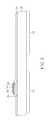
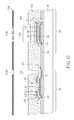
- FIG. 1illustrates a schematic diagram of a photo sensor of an amorphous silicon TFT display panel according to the present invention.
- the amorphous silicon TFT display panel 10includes a bottom substrate 34 and a top substrate 36 .
- the bottom substrate 34is normally referred to as an array substrate and the top substrate 36 is a color filter substrate.
- the TFT display panel 10may also be other types of flat display panels, such as an OLED display panel.
- the amorphous silicon TFT display panel 10further includes a display region 14 and a peripheral circuit region 12 , where the display region 14 includes a plurality of scan lines 20 and signal lines 18 , which define a plurality of pixels 16 arranged in matrix. Each pixel 16 includes a TFT 76 electrically connected to the scan line 20 and the signal line 18 .
- the TFT display panel 10also includes at least a photo sensor disposed in a sensor region 28 disposed in the periphery of the display region 14 .
- the photo sensorincludes ambient light sensors (ALS) 22 , 24 , 26 electrically connected to pads 32 disposed on the surface of the bottom substrate 34 via the conductive lines 30 .
- ALSambient light sensors
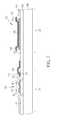
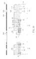
- FIGS. 2-7illustrate cross-sectional views of a method for forming a photo sensor on an amorphous silicon TFT display panel according to a first embodiment of the present invention.
- a substrate 38is provided.
- the substrate 38which may be an array substrate of a flat display panel, includes at least a TFT region 50 , and at least a sensor region 52 .
- a first conductive layeris then entirely deposited on the substrate 38 , and a first photolithographic and etching process using a first mask is performed to form a first patterned conductive layer 54 .
- the first pattern conductive layer 54is preferably metal material, and includes a gate electrode 56 disposed in the TFT region 50 . As shown in FIG.
- a gate insulating layer 58is deposited on the substrate 38 and the gate electrode 56 , and an amorphous silicon layer and a doped amorphous silicon layer are consecutively formed on the gate insulating layer 58 .
- a second photolithographic and etching process using a second maskis performed to pattern the amorphous silicon layer and the doped amorphous silicon layer to form a patterned amorphous silicon layer 60 and a patterned doped amorphous silicon layer 62 on the gate insulating layer 58 corresponding to the gate electrode 56 , where the patterned amorphous silicon layer 60 includes a semiconductor channel of a TFT.
- a second conductive layer 64 , and a silicon-rich dielectric layer 66 containing silicon-rich atomsare consecutively formed on the substrate 38 .
- the silicon-rich dielectric layer 66is a dielectric layer with excellent photosensitivity, and is a compound of silicon, oxygen, nitrogen, carbon, or hydrogen.
- a first photoresist layer(not shown) is coated on the substrate 38 , and a third photolithographic and etching process using a third mask is performed to define the pattern corresponding to the sensor region 52 .
- the silicon-rich dielectric layer 66is partially removed by dry or wet etching to form the patterned silicon-rich dielectric layer 66 in the sensor region 52 , and the first photoresist layer is then removed. It is appreciated that the molecular formula of the silicon-rich dielectric layer 66 includes SiOC, SiC, SiOx, SiNx, SiONy, SiOH, or any combination thereof.
- the silicon-rich dielectric layer 66may be formed by introducing gases containing silicon, oxygen, nitrogen, carbon, hydrogen, or a mixture thereof and then performing a chemical vapor deposition (CVD) process.
- the silicon-rich dielectric layer 66 containing SiOxmay be formed by implementing a CVD process introducing SiH 4 /N 2 O, or the silicon-rich dielectric layer 66 containing SiOH may be formed by implementing a CVD process introducing SiH 4 /N 2 O/H 2 .
- the silicon-rich dielectric layer 66is photosensitive, and therefore the composition may be adjusted to control the photosensitivity with respect to light beams of different colors.
- a laser annealing processmay be selectively performed when forming the silicon-rich dielectric layer 66 to form silicon nanocrystals in the silicon-rich dielectric layer 66 .
- a second photoresist layer(not shown) is formed on the substrate 38 , and a fourth photolithographic and etching process using a fourth mask is performed.
- the second conductive layer 64 not covered by the second photoresist layeris removed by dry or wet etching to form a second patterned conductive layer 64 ′, which includes a source electrode 70 and a drain electrode 72 electrically disconnected to each other in the TFT region 50 , and a bottom electrode 74 of a photo sensor in the sensor region 52 .
- a portion of the doped amorphous silicon layer 62is also removed in the fourth photolithographic and etching process, and the source electrode 70 and the drain electrode 72 are respectively electrically connected to the patterned amorphous silicon layer 60 via the remaining doped amorphous silicon layer 62 . Accordingly, a TFT 76 is formed on the substrate 38 .
- the bottom electrode 74 disposed in the sensor region 52is under the patterned silicon-rich dielectric layer 66 , and electrically connected to the silicon-rich dielectric layer 66 . It is appreciated that the sequence of the third and fourth photolithographic and etching processes may be swapped.
- the fourth photolithographic and etching processcan be immediately carried out to pattern the second conductive layer 64 to form a second patterned conductive layer 64 ′ including the source electrode 70 , the drain electrode 72 , and the bottom electrode 74 .
- the silicon-rich dielectric layer 66is formed, and the third photolithographic and etching process is performed to form the pattern silicon-rich dielectric layer 66 in the sensor region 52 .
- a passivation layer 78 with good water resistanceis entirely deposited on the substrate 38 .
- the passivation layer 78may include inorganic material e.g. silicon nitride or silicon oxide.
- a fifth photolithographic and etching process using a fifth maskis performed to partially remove the passivation layer 78 to form a through hole 80 , and to expose a portion of the drain electrode 72 and most part of the patterned silicon-rich dielectric layer 66 .
- a transparent conductive layersuch as indium tin oxide (ITO) or indium zinc oxide (IZO) is deposited, and a sixth photolithographic and etching process using a six mask is implemented to form a patterned transparent conductive layer 82 .
- the patterned transparent conductive layer 82includes a pixel electrode 84 disposed in the TFT region 50 , and a top electrode 86 disposed in the sensor region 52 .
- the pixel electrode 84is electrically connected to the drain electrode 72 via the patterned transparent conductive layer 82 filled into the through hole 80 .
- the top electrode 86is disposed on the surface of the silicon-rich dielectric layer 66 , and the top electrode 86 , the silicon-rich dielectric layer 66 , and the bottom electrode 74 constitute a photo sensor 88 .
- FIG. 8illustrates a cross-sectional view of a method for forming a photo sensor on an amorphous silicon TFT display panel according to a second embodiment of the present invention, where FIG. 8 follows the steps described in FIG. 5 of the first embodiment.
- organic materialis used to replace the passivation layer 78 of the first embodiment.
- a planarization layer 90which serves as a passivation of the TFT 76 , is formed on the substrate 38 to cover the TFT 76 and the silicon-rich dielectric layer 66 .
- the planarization layer 90includes photoresist material e.g. organic photoresist layer. Then, an exposure and development is implemented to pattern the planarization layer 90 to form through holes 80 , 92 , where the through hole 80 partially exposes the drain electrode 72 , and the through hole 92 partially exposes the silicon-rich dielectric layer 66 . Subsequently, a patterned transparent conductive layer 82 covering the drain electrode 72 exposed by the through hole 80 in the TFT region 50 , and covering the silicon-rich dielectric layer 66 exposed by the through hole 92 in the sensor region 52 is formed as described in the first embodiment. The portion of the patterned transparent conductive layer 82 electrically connected to the silicon-rich dielectric layer 66 serves as a top electrode 56 . Accordingly, the photo sensor 88 integrated into the fabrication of amorphous silicon TFT 76 is completed.
- photoresist materiale.g. organic photoresist layer.
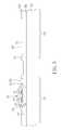
- FIGS. 9-10illustrate a method of forming a photo sensor according to a third embodiment of the present invention, where FIG. 9 follows FIG. 3 .
- a second patterned conductive layer 64 ′ including a source electrode 70 , a drain electrode 72 and a bottom electrode 74is formed on the substrate 38 .
- the second patterned conductive layer 64 ′may be formed by the following steps. First, a second conductive layer (as the second conductive layer 64 shown in FIG. 4 ) and a photoresist layer (not shown) are entirely deposited on the substrate 38 .
- a photolithographic and etching processis performed to partially remove the second conductive layer 64 and the doped amorphous silicon layer 62 .
- a patterned passivation layer 78 including a through hole 80 partially exposing the drain electrode 72 and a through hole 92 exposing most of the bottom electrode 74is formed on the substrate 38 .
- a silicon-rich dielectric layer 66is formed on the substrate 38 .
- a photolithographic and etching processis performed to partially remove the silicon-rich dielectric layer 66 so that the patterned silicon-rich dielectric layer 66 is disposed in the sensor region 52 .
- the silicon-rich dielectric layer 66may be both in the sensor region 52 and in the TFT region 50 .
- a patterned transparent conductive layer 82 including a pixel electrode 84 electrically connected to the drain electrode 72 , and a top electrode 86 of the photo sensor 88 electrically connected to the silicon-rich dielectric layer 66is formed on the substrate 38 .
- the passivation layer 78is formed prior to forming the silicon-rich dielectric layer 66 on the substrate 38 in this embodiment.
- the silicon-rich dielectric layer 66is formed in the TFT region 50 as well as in the sensor region 52 .
- FIG. 11illustrates a method for forming a photo sensor according to a fourth embodiment of the present invention, where FIG. 11 follows the fabrication of FIG. 9 . As shown in FIG. 11 , after forming the TFT 76 and the passivation layer 78 , a patterned silicon-rich dielectric layer 66 is formed on the substrate 38 .
- the silicon-rich dielectric layer 66includes a first part 66 a disposed in the sensor region 52 , and a second part 66 b disposed in the TFT region 50 , where the first part 66 a is used as the photosensitive material of the photo sensor 88 , and the second part 66 b is used as another passivation layer of the TFT 76 , the source electrode 70 and the drain electrode 72 .
- the patterned silicon-rich dielectric layer 66may be formed by the following steps. First, a silicon-rich dielectric layer 66 is entirely deposited on the substrate 38 .
- a photolithographic and etching processis performed to partially remove the silicon-rich dielectric layer 66 to form a first part 66 a in the sensor region 52 , and a second part 66 b in the TFT region 50 .
- a patterned transparent conductive layer 82 including a top electrode 86 corresponding to the sensor region 52 , and a pixel electrode 84 corresponding to the TFT region 50is formed on the substrate 38 .
- FIGS. 12-13illustrate a method of forming a photo sensor according to a fifth embodiment of the present invention.
- the silicon-rich dielectric layer 66replaces the passivation layer 78 of the third embodiment.
- FIG. 12follows the fabrication illustrated in FIG. 9 .
- a second patterned conductive layer 64 ′ including a source electrode 70 , a drain electrode 72 and a bottom electrode 74is formed on the substrate 38 , and the doped amorphous silicon layer 62 is partially removed to form a TFT 76 .
- a silicon-rich dielectric layer 96is entirely deposited, and then partially removed by photolithographic and etching techniques so that the remaining silicon-rich dielectric layer 96 covers most part of the TFT 76 and the bottom electrode 74 , and a through hole 94 is formed to partially expose the drain electrode 72 .
- a patterned transparent conductive layer 82is formed on the substrate 38 , where the patterned transparent conductive layer 82 includes a pixel electrode 84 electrically connected to the drain electrode 72 , and a top electrode 86 disposed in the sensor region 52 . Accordingly, the photo sensor 88 integrated into the fabrication of the amorphous silicon TFT 76 according to the fifth embodiment is completed.
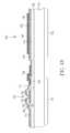
- FIGS. 14-19illustrate a method of forming a photo sensor according to a sixth embodiment of the present invention.
- this embodimentrequires only four masks to fabricate the photo sensor in the amorphous silicon TFT display panel.
- identical componentsare denoted by identical numerals.
- a substrate 38 having a TFT region 50 and a sensor region 52 defined thereonis provided.
- a first conductive layeris deposited on the substrate 38 , and patterned by performing a photolithographic and etching process using a first mask to form a first patterned conductive layer 54 including a gate electrode 56 disposed in the TFT region 50 .
- the first patterned conductive layer 54may further include a conductive line 98 disposed in the sensor region 52 .
- the first pattern conductive layer 54may exclude the conductive line 98 of the sensor region 52 in other embodiment.
- a gate insulating layer 58 covering the gate electrode 56 and the conductive line 98is formed on the substrate 38 .
- an amorphous silicon layer 100 , a doped amorphous silicon layer 62 , a second conductive layer 64 , and a silicon-rich dielectric layer 66are consecutively formed on the substrate 38 .
- a photoresist layer 218is then formed on the substrate 38 , and a second mask 216 is used to define the locations of a source electrode 70 , a drain electrode 72 , a semiconductor channel 68 (i.e. semiconductor region), a photosensitive material of the photo sensor, a bottom electrode 74 to be formed.
- the second maskmay include a graytone mask, a halftone mask or a phase shift mask.
- the second mask 216When the second mask 216 is a halftone mask, the second mask 216 includes an opaque region 216 a corresponding to the source electrode 70 , the drain electrode 72 and the bottom electrode 74 to be formed, a translucent region 216 b corresponding to the semiconductor channel to be formed, and a transparent region 216 c corresponding to the region other than the TFT region 50 and the sensor region 52 . As shown in FIG.
- an etching processis performed to remove the silicon-rich dielectric layer 66 , the second conductive layer 64 ′, the doped amorphous silicon layer 62 and the amorphous silicon layer 100 not covered by the photoresist layer 218 , so as to form the semiconductor channel 68 , the source electrode 70 , the drain electrode 72 , the bottom electrode 74 , and the patterned silicon-rich dielectric layer 66 .
- the silicon-rich dielectric layer 66includes a first part 66 a disposed in the sensor region 52 and over the surface of the bottom electrode 74 , and a second part 66 b disposed on the source electrode 70 and the drain electrode 72 , where the first part 66 a has a pattern of photosensitive material.
- the photoresist layer 218is removed, and a passivation layer 78 and a photoresist layer 102 are consecutively formed on the substrate 38 .
- a third mask 104is used to perform a photolithographic process upon the photoresist layer 102 .
- the third mask 104may include a graytone mask, a halftone mask or a phase shift mask.
- the third mask 104includes a translucent region 104 a substantially corresponding to the first part 66 a of the silicon-rich dielectric layer 66 in the sensor region 52 , and a transparent region 104 b corresponding to the location corresponding to the drain electrode 74 where a through hole pattern is to be formed.
- a development processis implemented to pattern the photoresist layer 102 to form a through hole pattern 106 and an opening pattern 108 , where the through hole pattern 106 partially exposes the passivation layer 78 .
- an anisotropic etching processis performed using the patterned photoresist layer 102 as an etching mask to partially remove the passivation layer 78 and the silicon-rich dielectric layer 66 so as to form a through hole 110 in the TFT region 50 , and an opening 112 in the sensor region 52 .
- the through hole 110partially exposes the drain electrode 72
- the opening 112partially exposes the first part 66 a of the silicon-rich dielectric layer 66 .
- a pattern transparent conductive layer 82is formed on the substrate 38 by the following steps.
- a transparent conductive layer and a photoresist layer(not shown) are entirely formed on the substrate 38 , and a photolithographic and etching process using a fourth mask is carried out to partially remove the transparent conductive layer, thereby forming a pixel electrode 84 filling into the through hole 110 and electrically connected to the drain electrode 72 in the TFT region 50 , and a top electrode 86 filling into the opening 112 and disposed on the surface of the first part 66 a of the silicon-rich dielectric layer 66 in the sensor region 52 .
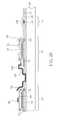
- FIGS. 20-23illustrate a method of forming a photo sensor integrated into the fabrication of an amorphous silicon TFT according to a seventh embodiment of the present invention.
- itrequires only three masks and three photolithographic processes to fabricate the photo sensor and the TFT in the amorphous silicon TFT display panel.
- a substrate 38 having a TFT region 50 , a sensor region 52 , and a pad region 114 defined thereonis provide.
- a TFT 76 and a silicon-rich dielectric layer 66are formed as described in FIGS. 14-16 .
- a bottom pad 116is formed simultaneously with the gate electrode 56 , and the gate insulating layer 58 is formed to cover the bottom pad 116 in the pad region 114 as well as the gate electrode 56 .
- the steps illustrated in FIG. 16is completed, and the photoresist layer 218 is removed.
- a passivation layer 78 and a photoresist layer 118are consecutively formed on the substrate 38 , and a photolithographic and development process using a third mask 126 is performed to pattern the photoresist layer 118 . Accordingly, an opening pattern 120 , a through hole pattern 122 and a pad pattern 124 are defined in the photoresist layer 118 .
- the third mask 126includes an opaque region 126 a corresponding to a portion of the passivation layer 78 to be reserved, a transparent region 126 c corresponding to the pad pattern 124 and the through hole pattern 122 , and a translucent region 126 b corresponding to the opening pattern 120 and selectively corresponding to one side of the through hole pattern 122 and the edge of the sensor region 52 wherever necessary.
- an etching processis performed using the patterned photoresist layer 118 as an etching mask to partially remove the passivation layer 78 , the silicon-rich dielectric layer 66 , and the gate insulating layer 58 .
- an opening 128is formed in the passivation layer 78 in the sensor region 52 , a through hole 130 partially exposing the drain electrode 72 is formed, a pad opening 132 exposing the bottom pad 116 is formed, and a portion of the photoresist layer 118 ′ corresponding to the opaque region 126 a is reserved.
- a transparent conductive layer 134is entirely formed on the substrate 38 . As shown in FIG.
- a lift-off processis performed to remove the photoresist layer 118 ′ and the transparent conductive layer 134 disposed on the surface of the photoresist layer 118 ′ simultaneously, and the transparent conductive layer 134 ′ not disposed on the photoresist layer 118 ′ is reserved.
- the remaining transparent conductive layer 134includes a top electrode 86 disposed in the sensor region 52 , a pixel electrode 84 electrically connected to the drain electrode 72 in the TFT region 50 , and a top pad 136 in the pad region 114 , where the top pad 136 and the bottom pad 116 are electrically connected together, forming a pad 32 as shown in FIG. 1 .
- the photo sensorcan be formed with only three to six masks, integrated into the fabrication of TFT of the amorphous silicon TFT display panel, and therefore the process steps are simplified and the cost is reduced.
- the photo sensor of the present inventioncan be formed outside the display region of the display panel and used as an ALS, or can also be formed inside each pixel of the display region and used as a color image sensor by co-operating with the color filters of the display panel or by adjusting the pattern of the photosensitive material of the silicon-rich dielectric layer.
- the amorphous silicon TFT display panelcan be an optical touch panel or a finger print sensor by connecting the photo current generated by the photo sensor to related circuit design.
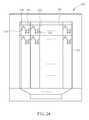
- FIG. 24illustrates a circuit diagram of an optical touch panel or a finger print sensor using the photo sensor of the present invention.
- the optical touch panel 200includes a display region 202 , a plurality of signal lines 204 and read-out lines 212 arranged in parallel, a plurality of scan lines 206 perpendicular to the signal lines 204 , and a plurality of pixels 208 defined by the signal lines 204 and the scan lines 206 and arranged in matrix.
- Each of the pixels 208includes a TFT 214 electrically connected to the signal line 204 , and at least a photo sensor 210 electrically connected to the read-out line 212 .
- the photo sensor using silicon-rich dielectric materialhas excellent product reliability.
- the signal-to-noise ratiocan reach 200 to 300 when used in UV-blue sensors.
- the process of forming the photo sensor using silicon-rich dielectric materialis integrated into the process of amorphous silicon TFT. By virtue of redesigning the sequence of photolithographic process and deposition process, the process steps, manufacturing cost, and cycle time can be reduced.
- the photo sensor using silicon-rich dielectric materialcan be used in touch panel, which can reduce the manufacturing cost of touch panel, and also provide value-added for the product.
Landscapes
- Thin Film Transistor (AREA)
- Solid State Image Pick-Up Elements (AREA)
Abstract
Description
Claims (23)
Applications Claiming Priority (3)
| Application Number | Priority Date | Filing Date | Title |
|---|---|---|---|
| TW97117078A | 2008-05-09 | ||
| TW097117078ATWI333275B (en) | 2008-05-09 | 2008-05-09 | Method for fabricating light sensor |
| TW097117078 | 2008-05-09 |
Publications (2)
| Publication Number | Publication Date |
|---|---|
| US20090280606A1 US20090280606A1 (en) | 2009-11-12 |
| US7790487B2true US7790487B2 (en) | 2010-09-07 |
Family
ID=41267179
Family Applications (1)
| Application Number | Title | Priority Date | Filing Date |
|---|---|---|---|
| US12/211,106Active2028-12-04US7790487B2 (en) | 2008-05-09 | 2008-09-16 | Method for fabricating photo sensor |
Country Status (2)
| Country | Link |
|---|---|
| US (1) | US7790487B2 (en) |
| TW (1) | TWI333275B (en) |
Cited By (17)
| Publication number | Priority date | Publication date | Assignee | Title |
|---|---|---|---|---|
| US20100315570A1 (en)* | 2009-06-11 | 2010-12-16 | Mathew Dinesh C | Portable computer display structures |
| US20100327289A1 (en)* | 2009-06-29 | 2010-12-30 | An-Thung Cho | Flat display panel, uv sensor and fabrication method thereof |
| US20110193067A1 (en)* | 2010-02-09 | 2011-08-11 | Samsung Mobile Display Co., Ltd. | Organic light-emitting device including barrier layer including silicon oxide layer and silicon-rich silicon nitride layer |
| US20110221720A1 (en)* | 2010-03-11 | 2011-09-15 | Au Optronics Corporation | Amoled display with optical feedback compensation |
| US8408780B2 (en) | 2009-11-03 | 2013-04-02 | Apple Inc. | Portable computer housing with integral display |
| US8467177B2 (en) | 2010-10-29 | 2013-06-18 | Apple Inc. | Displays with polarizer windows and opaque masking layers for electronic devices |
| US20140014847A1 (en)* | 2012-07-12 | 2014-01-16 | Carestream Health, Inc. | Radiographic imaging array fabrication process for metal oxide thin-film transistors with reduced mask count |
| US8743309B2 (en) | 2009-11-10 | 2014-06-03 | Apple Inc. | Methods for fabricating display structures |
| US8765514B1 (en)* | 2010-11-12 | 2014-07-01 | L-3 Communications Corp. | Transitioned film growth for conductive semiconductor materials |
| TWI460841B (en)* | 2012-07-13 | 2014-11-11 | Au Optronics Corp | Photo sensor type touch display panel |
| US9142804B2 (en) | 2010-02-09 | 2015-09-22 | Samsung Display Co., Ltd. | Organic light-emitting device including barrier layer and method of manufacturing the same |
| US9143668B2 (en) | 2010-10-29 | 2015-09-22 | Apple Inc. | Camera lens structures and display structures for electronic devices |
| US9330846B2 (en) | 2012-09-07 | 2016-05-03 | E Ink Holdings Inc. | Capacitor structure of capacitive touch panel |
| US11632448B2 (en) | 2019-12-03 | 2023-04-18 | Apple Inc. | Handheld electronic device |
| US11637919B2 (en) | 2019-12-03 | 2023-04-25 | Apple Inc. | Handheld electronic device |
| US12003657B2 (en) | 2021-03-02 | 2024-06-04 | Apple Inc. | Handheld electronic device |
| US12267449B2 (en) | 2022-03-03 | 2025-04-01 | Apple Inc. | Handheld electronic device |
Families Citing this family (19)
| Publication number | Priority date | Publication date | Assignee | Title |
|---|---|---|---|---|
| US7857907B2 (en)* | 2007-01-25 | 2010-12-28 | Au Optronics Corporation | Methods of forming silicon nanocrystals by laser annealing |
| US20080179762A1 (en)* | 2007-01-25 | 2008-07-31 | Au Optronics Corporation | Layered structure with laser-induced aggregation silicon nano-dots in a silicon-rich dielectric layer, and applications of the same |
| KR101571045B1 (en)* | 2008-12-26 | 2015-11-24 | 삼성디스플레이 주식회사 | Thin film transistor array substrate for X-ray detector and manufacturing method thereof |
| TWI389256B (en)* | 2009-04-17 | 2013-03-11 | Au Optronics Corp | Active element array substrate manufacturing method |
| JP5823740B2 (en)* | 2010-06-16 | 2015-11-25 | 株式会社半導体エネルギー研究所 | Input/Output Devices |
| TWI453805B (en)* | 2011-02-11 | 2014-09-21 | Au Optronics Corp | Display and its making method |
| CN102790068B (en)* | 2012-07-26 | 2014-10-22 | 北京京东方光电科技有限公司 | Manufacturing method for sensor |
| TWI472981B (en)* | 2012-11-30 | 2015-02-11 | Hannstouch Solution Inc | Touch panel and manufacturing method thereof |
| KR102103421B1 (en) | 2013-02-07 | 2020-04-23 | 삼성디스플레이 주식회사 | Organic light emitting diode device and manufacturing method thereof |
| KR102097031B1 (en)* | 2013-07-22 | 2020-04-06 | 삼성디스플레이 주식회사 | Foldable display and method of manufacturing the same |
| TWI561894B (en)* | 2015-05-29 | 2016-12-11 | Hon Hai Prec Ind Co Ltd | Manufacturing method of making electronic connection structure, tft substrate, and insulation layer |
| TWI574374B (en) | 2015-09-09 | 2017-03-11 | 友達光電股份有限公司 | Method of fabricating optical sensing element and thin film transistor element |
| KR102555180B1 (en) | 2016-11-30 | 2023-07-13 | 엘지디스플레이 주식회사 | Touch display device, display panel, and all in one switch device |
| CN107863319B (en)* | 2017-09-25 | 2021-04-02 | 惠科股份有限公司 | An array substrate and its manufacturing method |
| CN107863353A (en)* | 2017-09-25 | 2018-03-30 | 惠科股份有限公司 | Array substrate and manufacturing method thereof |
| CN107643657B (en)* | 2017-10-31 | 2019-10-11 | 武汉华星光电技术有限公司 | A method and mask for improving TITO residue on the periphery of a panel |
| KR102526246B1 (en)* | 2017-11-17 | 2023-04-26 | 엘지디스플레이 주식회사 | Driving circuit, display panel and display device |
| TWI652534B (en)* | 2017-12-21 | 2019-03-01 | 友達光電股份有限公司 | Pixel structure and display panel |
| CN113743162B (en)* | 2020-05-29 | 2024-10-15 | 京东方科技集团股份有限公司 | Sensor, display panel, and display device |
Citations (12)
| Publication number | Priority date | Publication date | Assignee | Title |
|---|---|---|---|---|
| US5075244A (en) | 1989-11-16 | 1991-12-24 | Fuji Xerox Co., Ltd. | Method of manufacturing image sensors |
| US5466617A (en)* | 1992-03-20 | 1995-11-14 | U.S. Philips Corporation | Manufacturing electronic devices comprising TFTs and MIMs |
| US5530265A (en)* | 1993-08-12 | 1996-06-25 | Semiconductor Energy Laboratory Co., Ltd. | Insulated gate semiconductor device and process for fabricating the same |
| US6100951A (en)* | 1996-09-30 | 2000-08-08 | U.S. Philips Corporation | Thin-film switching elements for electronic devices and a method of manufacturing the same |
| US6407393B1 (en) | 1999-04-01 | 2002-06-18 | Lg. Philips Lcd Co., Ltd. | X-ray image sensor and method for fabricating the same |
| US20060180816A1 (en) | 2005-02-14 | 2006-08-17 | Sharp Laboratories Of America, Inc. | Wide wavelength range silicon electroluminescence device |
| US20060205102A1 (en)* | 2002-12-19 | 2006-09-14 | Koninklijke Philips Electronics N.V. | Liquid crystal displays |
| US7221039B2 (en)* | 2004-06-24 | 2007-05-22 | Taiwan Semiconductor Manufacturing Co., Ltd. | Thin film transistor (TFT) device structure employing silicon rich silicon oxide passivation layer |
| US20090009675A1 (en)* | 2007-01-25 | 2009-01-08 | Au Optronics Corporation | Photovoltaic Cells of Si-Nanocrystals with Multi-Band Gap and Applications in a Low Temperature Polycrystalline Silicon Thin Film Transistor Panel |
| US20090153056A1 (en)* | 2007-12-17 | 2009-06-18 | Au Optronics Corporation | Pixel structure, display panel, eletro-optical apparatus, and method thererof |
| US20090283850A1 (en)* | 2008-05-16 | 2009-11-19 | An-Thung Cho | Optical sensor and method of making the same |
| US20100012937A1 (en)* | 2008-07-21 | 2010-01-21 | Au Optronics Corporation | Thin film transistor array substrate and method for fabricating the same |
- 2008
- 2008-05-09TWTW097117078Apatent/TWI333275B/enactive
- 2008-09-16USUS12/211,106patent/US7790487B2/enactiveActive
Patent Citations (12)
| Publication number | Priority date | Publication date | Assignee | Title |
|---|---|---|---|---|
| US5075244A (en) | 1989-11-16 | 1991-12-24 | Fuji Xerox Co., Ltd. | Method of manufacturing image sensors |
| US5466617A (en)* | 1992-03-20 | 1995-11-14 | U.S. Philips Corporation | Manufacturing electronic devices comprising TFTs and MIMs |
| US5530265A (en)* | 1993-08-12 | 1996-06-25 | Semiconductor Energy Laboratory Co., Ltd. | Insulated gate semiconductor device and process for fabricating the same |
| US6100951A (en)* | 1996-09-30 | 2000-08-08 | U.S. Philips Corporation | Thin-film switching elements for electronic devices and a method of manufacturing the same |
| US6407393B1 (en) | 1999-04-01 | 2002-06-18 | Lg. Philips Lcd Co., Ltd. | X-ray image sensor and method for fabricating the same |
| US20060205102A1 (en)* | 2002-12-19 | 2006-09-14 | Koninklijke Philips Electronics N.V. | Liquid crystal displays |
| US7221039B2 (en)* | 2004-06-24 | 2007-05-22 | Taiwan Semiconductor Manufacturing Co., Ltd. | Thin film transistor (TFT) device structure employing silicon rich silicon oxide passivation layer |
| US20060180816A1 (en) | 2005-02-14 | 2006-08-17 | Sharp Laboratories Of America, Inc. | Wide wavelength range silicon electroluminescence device |
| US20090009675A1 (en)* | 2007-01-25 | 2009-01-08 | Au Optronics Corporation | Photovoltaic Cells of Si-Nanocrystals with Multi-Band Gap and Applications in a Low Temperature Polycrystalline Silicon Thin Film Transistor Panel |
| US20090153056A1 (en)* | 2007-12-17 | 2009-06-18 | Au Optronics Corporation | Pixel structure, display panel, eletro-optical apparatus, and method thererof |
| US20090283850A1 (en)* | 2008-05-16 | 2009-11-19 | An-Thung Cho | Optical sensor and method of making the same |
| US20100012937A1 (en)* | 2008-07-21 | 2010-01-21 | Au Optronics Corporation | Thin film transistor array substrate and method for fabricating the same |
Cited By (45)
| Publication number | Priority date | Publication date | Assignee | Title |
|---|---|---|---|---|
| US20210223822A1 (en)* | 2009-06-11 | 2021-07-22 | Apple Inc. | Portable Computer Display Structures |
| US11740658B2 (en)* | 2009-06-11 | 2023-08-29 | Apple Inc. | Portable computer display structures |
| US12189424B2 (en)* | 2009-06-11 | 2025-01-07 | Apple Inc. | Portable computer display structures |
| US20230350457A1 (en)* | 2009-06-11 | 2023-11-02 | Apple Inc. | Portable computer display structures |
| US20120020002A1 (en)* | 2009-06-11 | 2012-01-26 | Mathew Dinesh C | Portable computer display structures |
| US20120020000A1 (en)* | 2009-06-11 | 2012-01-26 | Mathew Dinesh C | Portable computer display structures |
| US20150138710A1 (en)* | 2009-06-11 | 2015-05-21 | Apple Inc. | Portable Computer Display Structures |
| US8395722B2 (en)* | 2009-06-11 | 2013-03-12 | Apple Inc. | Portable computer display structures |
| US20100315570A1 (en)* | 2009-06-11 | 2010-12-16 | Mathew Dinesh C | Portable computer display structures |
| US10353432B2 (en) | 2009-06-11 | 2019-07-16 | Apple Inc. | Portable computer display structures |
| US8456586B2 (en)* | 2009-06-11 | 2013-06-04 | Apple Inc. | Portable computer display structures |
| US20130188305A1 (en)* | 2009-06-11 | 2013-07-25 | Apple Inc. | Portable Computer Display Structures |
| US8866989B2 (en)* | 2009-06-11 | 2014-10-21 | Apple Inc. | Portable computer display structures |
| US11003213B2 (en) | 2009-06-11 | 2021-05-11 | Apple Inc. | Portable computer display structures |
| US8711304B2 (en)* | 2009-06-11 | 2014-04-29 | Apple Inc. | Portable computer display structures |
| US20100327289A1 (en)* | 2009-06-29 | 2010-12-30 | An-Thung Cho | Flat display panel, uv sensor and fabrication method thereof |
| US8344381B2 (en)* | 2009-06-29 | 2013-01-01 | Au Optronics Corp. | Flat display panel, UV sensor and fabrication method thereof |
| US8408780B2 (en) | 2009-11-03 | 2013-04-02 | Apple Inc. | Portable computer housing with integral display |
| US9069525B2 (en) | 2009-11-10 | 2015-06-30 | Apple Inc. | Methods for fabricating display structures |
| US9575354B2 (en) | 2009-11-10 | 2017-02-21 | Apple Inc. | Methods for fabricating display structures |
| US8767141B2 (en) | 2009-11-10 | 2014-07-01 | Apple Inc. | Methods for fabricating display structures |
| US10983390B2 (en) | 2009-11-10 | 2021-04-20 | Apple Inc. | Methods for fabricating display structures |
| US8743309B2 (en) | 2009-11-10 | 2014-06-03 | Apple Inc. | Methods for fabricating display structures |
| US10261540B2 (en) | 2009-11-10 | 2019-04-16 | Apple Inc. | Methods for fabricating display structures |
| US9324776B2 (en) | 2010-02-09 | 2016-04-26 | Samsung Display Co., Ltd. | Organic light-emitting device including barrier layer including silicon oxide layer and silicon nitride layer |
| US9142804B2 (en) | 2010-02-09 | 2015-09-22 | Samsung Display Co., Ltd. | Organic light-emitting device including barrier layer and method of manufacturing the same |
| US20110193067A1 (en)* | 2010-02-09 | 2011-08-11 | Samsung Mobile Display Co., Ltd. | Organic light-emitting device including barrier layer including silicon oxide layer and silicon-rich silicon nitride layer |
| US20110221720A1 (en)* | 2010-03-11 | 2011-09-15 | Au Optronics Corporation | Amoled display with optical feedback compensation |
| US8669924B2 (en) | 2010-03-11 | 2014-03-11 | Au Optronics Corporation | Amoled display with optical feedback compensation |
| US10009525B2 (en) | 2010-10-29 | 2018-06-26 | Apple Inc. | Camera lens structures and display structures for electronic devices |
| US11188118B2 (en) | 2010-10-29 | 2021-11-30 | Apple Inc. | Displays with polarizer windows and opaque masking layers for electronic devices |
| US9372505B2 (en) | 2010-10-29 | 2016-06-21 | Apple Inc. | Displays with polarizer windows and opaque masking layers for electronic devices |
| US10571957B2 (en) | 2010-10-29 | 2020-02-25 | Apple Inc. | Displays with polarizer windows and opaque masking layers for electronic devices |
| US8467177B2 (en) | 2010-10-29 | 2013-06-18 | Apple Inc. | Displays with polarizer windows and opaque masking layers for electronic devices |
| US9143668B2 (en) | 2010-10-29 | 2015-09-22 | Apple Inc. | Camera lens structures and display structures for electronic devices |
| US8765514B1 (en)* | 2010-11-12 | 2014-07-01 | L-3 Communications Corp. | Transitioned film growth for conductive semiconductor materials |
| US20140014847A1 (en)* | 2012-07-12 | 2014-01-16 | Carestream Health, Inc. | Radiographic imaging array fabrication process for metal oxide thin-film transistors with reduced mask count |
| US9048160B2 (en)* | 2012-07-12 | 2015-06-02 | Carestream Health, Inc. | Radiographic imaging array fabrication process for metal oxide thin-film transistors with reduced mask count |
| US9911771B2 (en) | 2012-07-12 | 2018-03-06 | Carestream Health, Inc. | Radiographic imaging array fabrication process for metal oxide thin-film transistors with reduced mask count |
| TWI460841B (en)* | 2012-07-13 | 2014-11-11 | Au Optronics Corp | Photo sensor type touch display panel |
| US9330846B2 (en) | 2012-09-07 | 2016-05-03 | E Ink Holdings Inc. | Capacitor structure of capacitive touch panel |
| US11632448B2 (en) | 2019-12-03 | 2023-04-18 | Apple Inc. | Handheld electronic device |
| US11637919B2 (en) | 2019-12-03 | 2023-04-25 | Apple Inc. | Handheld electronic device |
| US12003657B2 (en) | 2021-03-02 | 2024-06-04 | Apple Inc. | Handheld electronic device |
| US12267449B2 (en) | 2022-03-03 | 2025-04-01 | Apple Inc. | Handheld electronic device |
Also Published As
| Publication number | Publication date |
|---|---|
| TW200947683A (en) | 2009-11-16 |
| TWI333275B (en) | 2010-11-11 |
| US20090280606A1 (en) | 2009-11-12 |
Similar Documents
| Publication | Publication Date | Title |
|---|---|---|
| US7790487B2 (en) | Method for fabricating photo sensor | |
| CN100543970C (en) | How to Make a Light Sensor | |
| US7439090B2 (en) | Method for manufacturing a lower substrate of a liquid crystal display device | |
| CN104749843B (en) | Array substrate and preparation method thereof, driving method and display device | |
| CN108336100B (en) | Array substrate and preparation method thereof, display panel, and display device | |
| US7413940B2 (en) | Thin-film transistor and fabrication method thereof | |
| TWI464808B (en) | Thin film transistor array substrate and manufacturing method thereof | |
| CN101022085B (en) | Semiconductor element and manufacturing method thereof | |
| US7645649B1 (en) | Method for fabricating pixel structure | |
| CN102709234B (en) | Thin-film transistor array base-plate and manufacture method thereof and electronic device | |
| CN103178119B (en) | Array base palte, array base palte preparation method and display unit | |
| CN101634789B (en) | Pixel structure and manufacturing method of pixel structure | |
| US9804463B2 (en) | Array substrate and fabrication method thereof and display device | |
| CN102629584B (en) | Array substrate and manufacturing method thereof and display device | |
| CN103033997B (en) | Display device and method for manufacturing the same | |
| WO2020210939A1 (en) | Touch display substrate, manufacturing method therefor, and display device | |
| CN112616321B (en) | Display substrate, manufacturing method thereof and display device | |
| US20060258080A1 (en) | Vertical diode, matrix position sensitive apparatus and manufacturing method of the same | |
| US10243010B2 (en) | Semiconductor substrate and display device | |
| US10868054B2 (en) | Photoelectric conversion substrate, manufacturing method of the same, display panel and display device | |
| US20120241746A1 (en) | Electrophoresis display and manufacturing method | |
| CN106298805A (en) | A kind of display floater and preparation method thereof and display device | |
| KR20060023327A (en) | Thin film transistor array substrate and manufacturing method thereof | |
| CN110729250A (en) | Array substrate manufacturing method and array substrate | |
| CN100559570C (en) | Method for manufacturing pixel structure |
Legal Events
| Date | Code | Title | Description |
|---|---|---|---|
| AS | Assignment | Owner name:AU OPTRONICS CORP., TAIWAN Free format text:ASSIGNMENT OF ASSIGNORS INTEREST;ASSIGNORS:SHIH, CHING-CHIEH;CHO, AN-THUNG;PENG, CHIA-TIEN;AND OTHERS;REEL/FRAME:021540/0818;SIGNING DATES FROM 20080903 TO 20080910 Owner name:AU OPTRONICS CORP., TAIWAN Free format text:ASSIGNMENT OF ASSIGNORS INTEREST;ASSIGNORS:SHIH, CHING-CHIEH;CHO, AN-THUNG;PENG, CHIA-TIEN;AND OTHERS;SIGNING DATES FROM 20080903 TO 20080910;REEL/FRAME:021540/0818 | |
| STCF | Information on status: patent grant | Free format text:PATENTED CASE | |
| FPAY | Fee payment | Year of fee payment:4 | |
| MAFP | Maintenance fee payment | Free format text:PAYMENT OF MAINTENANCE FEE, 8TH YEAR, LARGE ENTITY (ORIGINAL EVENT CODE: M1552) Year of fee payment:8 | |
| MAFP | Maintenance fee payment | Free format text:PAYMENT OF MAINTENANCE FEE, 12TH YEAR, LARGE ENTITY (ORIGINAL EVENT CODE: M1553); ENTITY STATUS OF PATENT OWNER: LARGE ENTITY Year of fee payment:12 | |
| AS | Assignment | Owner name:AUO CORPORATION, TAIWAN Free format text:CHANGE OF NAME;ASSIGNOR:AU OPTRONICS CORPORATION;REEL/FRAME:063785/0830 Effective date:20220718 | |
| AS | Assignment | Owner name:OPTRONIC SCIENCES LLC, TEXAS Free format text:ASSIGNMENT OF ASSIGNORS INTEREST;ASSIGNOR:AUO CORPORATION;REEL/FRAME:064658/0572 Effective date:20230802 |