US7786946B2 - Hollow dielectric pipe polyrod antenna - Google Patents
Hollow dielectric pipe polyrod antennaDownload PDFInfo
- Publication number
- US7786946B2 US7786946B2US12/004,729US472907AUS7786946B2US 7786946 B2US7786946 B2US 7786946B2US 472907 AUS472907 AUS 472907AUS 7786946 B2US7786946 B2US 7786946B2
- Authority
- US
- United States
- Prior art keywords
- dielectric
- conductor
- pipe
- dielectric pipe
- section
- Prior art date
- Legal status (The legal status is an assumption and is not a legal conclusion. Google has not performed a legal analysis and makes no representation as to the accuracy of the status listed.)
- Expired - Fee Related, expires
Links
Images


Classifications
- H—ELECTRICITY
- H01—ELECTRIC ELEMENTS
- H01Q—ANTENNAS, i.e. RADIO AERIALS
- H01Q13/00—Waveguide horns or mouths; Slot antennas; Leaky-waveguide antennas; Equivalent structures causing radiation along the transmission path of a guided wave
- H—ELECTRICITY
- H01—ELECTRIC ELEMENTS
- H01P—WAVEGUIDES; RESONATORS, LINES, OR OTHER DEVICES OF THE WAVEGUIDE TYPE
- H01P3/00—Waveguides; Transmission lines of the waveguide type
- H01P3/12—Hollow waveguides
- H01P3/123—Hollow waveguides with a complex or stepped cross-section, e.g. ridged or grooved waveguides
Definitions
- Broadband antennas or systems incorporating the sameare generally discussed herein, with particular discussions extended to a compact broadband antenna with a polyrod.
- a simple, reliable, broadband method for extracting constitutive property measurements from an electromagnetic material sampleoccurs under plane wave conditions. Therefore, the ability to mimic a plane wave condition at the material sample is of paramount importance. Performing such measurements in a small spot-size and a broad band of frequencies allows designers and users of electromagnetic materials to reliably determine the constitutive properties of material samples as a function of position, particularly graded impedance and resistance sheets (such as those used to reduce diffraction from edges of parabolic dish antennas).
- An aspect of an embodiment of the present inventionis directed toward an antenna capable of providing a relatively small spot-size in a plane wave condition.
- An embodiment of the present inventionprovides a waveguide including: a first section including a first surface facing a flange, a second surface oppositely facing away from the first surface, an upper wall, and a lower wall facing the upper wall; and a second section extending out from the second surface; wherein the first section includes an upper ridge disposed on the upper wall of the first section and a lower ridge disposed on the lower wall of the first section, wherein the second section includes an upper conductor extending out from a top portion of the second surface and a lower conductor extending out from a lower portion of the second surface with a gap between the upper conductor and the lower conductor, wherein the upper conductor is electrically connected to the upper ridge, wherein the lower conductor is electrically connected to the lower ridge, and wherein the upper conductor and the lower conductor are adapted to propagate a wave from the first section and to reduce a discontinuity of the wave propagated at a connection between the first section and the second section.
- the upper conductormay include an upper notch at a distal end away from the second surface, wherein the lower conductor may include a lower notch at a distal end away from the second surface, and wherein the upper and lower notches are configured to reduce reflection of the wave propagated by the upper conductor and the lower conductor.
- the second sectionmay consist essentially of the upper conductor extending out from the top portion of the second surface and the lower conductor extending out from the lower portion of the second surface with the gap between the upper conductor and the lower conductor.
- An embodiment of the present inventionprovides a waveguide including: a double-ridged waveguide section having a first ridge and a second ridge; a first conductor extending from the first ridge; and a second conductor extending from the second ridge; wherein the first and second conductors are configured to propagate a wave from the double-ridged waveguide section and to reduce a discontinuity of the wave propagated at a connection between the double-ridged waveguide section and the two conductors.
- the first conductormay include an upper notch at a distal end away from the double-ridged waveguide section, wherein the second conductor may include a lower notch at a distal end away from the double-ridged waveguide section, and wherein the upper and lower notches are configured to reduce reflection of the wave propagated by the upper conductor and the lower conductor.
- An embodiment of the present inventionprovides a dielectric pipe antenna including: a dielectric pipe; and a waveguide for receiving one end of the dielectric pipe; wherein the waveguide includes: a first section including a first surface facing a flange, a second surface oppositely facing away from the first surface, an upper wall, and a lower wall facing the upper wall; and a second section extending out from the second surface; wherein the first section includes an upper ridge disposed on the upper wall of the first section and a lower ridge disposed on the lower wall of the first section, wherein the second section includes an upper conductor extending out from a top portion of the second surface and a lower conductor extending out from a lower portion of the second surface with a gap between the upper conductor and the lower conductor, and wherein the dielectric pipe includes: a hollow tubular dielectric sleeve portion having an external sleeve diameter and an internal sleeve diameter; and a tapered dielectric pipe portion having an internal pipe diameter, a first outer pipe diameter at
- the dielectric pipemay have a dielectric constant ranging from about 1.5 to about 9.
- the dielectric pipemay have a dielectric constant ranging from about 2.5 to about 3.
- the hollow tubular dielectric sleeve portionmay surround and be electromagnetically coupled to the upper conductor and the lower conductor of the second section.
- a wave generated within the dielectric pipemay be substantially planar, and wherein a generated wave upon exiting the dielectric pipe may be substantially the same as the wave generated within the dielectric pipe surrounding the upper conductor and the lower conductor.
- the second sectionmay consist essentially of the upper conductor extending out from the top portion of the second surface and the lower conductor extending out from the lower portion of the second surface with the gap between the upper conductor and the lower conductor.
- Each of the upper conductor and the lower conductor of the second sectionmay have a length configured to maximize an electromagnetic coupling of the upper conductor and the lower conductor to the dielectric pipe surrounding the upper conductor and the lower conductor.
- the upper conductormay include an upper notch at a distal end away from the second surface, wherein the lower conductor may include a lower notch at a distal end away from the second surface, and wherein the upper and lower notches may be configured to reduce reflection of the wave propagated by the upper conductor and the lower conductor.
- a height of the first metallic section of the waveguidemay be about 0.473 inches, a width of the first metallic section of the waveguide may be about 0.833 inches, and each of the upper conductor and the lower conductor may have a length of about 1.476 inches, and wherein the height of the first metallic section, the width of the first metallic section, and the length of each of the upper conductor and the lower conductor may be configured to operate at frequency ranging from about 5.5 GHz to about 18 GHz.
- a length of the hollow tubular dielectric sleevemay be at about 2.952 inches, the internal sleeve diameter may be about 0.886 inches and a length of the tapered dielectric pipe portion may be at about 1.969 in, and wherein the length of the hollow tubular dielectric sleeve, the internal sleeve diameter, and the length of the tapered dielectric pipe portion may be configured to operate at a frequency range of about 5.5 GHz to about 18 GHz.
- a length of the hollow tubular dielectric sleeve, the internal sleeve diameter, a length of the tapered dielectric pipe portion and proportions of the double-ridged waveguidemay be configured to operate at a frequency range of about 100 MHz to about 100 GHz.
- the one end of the dielectric pipemay make a releasable-fit engagement with the second metallic section of the waveguide.
- An embodiment of the present inventionprovides a dielectric pipe antenna including: a dielectric pipe; and a waveguide for receiving one end of the dielectric pipe; wherein the waveguide includes: a double-ridged waveguide section having a first ridge and a second ridge; a first conductor extending from the first ridge; and a second conductor extending from the second ridge; wherein the dielectric pipe includes: a hollow tubular dielectric sleeve portion having an external sleeve diameter and an internal sleeve diameter; and a tapered dielectric pipe portion having an internal pipe diameter, a first outer pipe diameter at a first location of the tapered dielectric pipe portion, and a second outer pipe diameter at a second location of the tapered dielectric pipe portion, wherein the first outer pipe diameter is larger than the second outer pipe diameter, and wherein the first location is between the hollow tubular dielectric sleeve portion and the second location.
- the dielectric pipemay have a dielectric constant ranging from about 1.5 to about 9.
- the first conductormay include an upper notch at a distal end away from the double-ridged waveguide section, wherein the second conductor includes a lower notch at a distal end away from the double-ridged waveguide section, and wherein the upper and lower notches are configured to reduce reflection of the wave propagated by the upper conductor and the lower conductor.
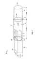
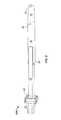
- FIG. 1is a perspective schematic view of an antenna of an embodiment of the present invention.
- FIG. 2is an antenna of an embodiment of the present invention.
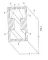
- FIG. 3is a perspective view of a double ridge waveguide.
- FIGS. 4 and 5are, respectively, a vector plot of a calculated E-field and associated contours of field strength, and a vector plot of a calculated H-field and associated contours of field strength of an antenna of an embodiment of the present invention.
- FIG. 6is a schematic cross-sectional view of an antenna an embodiment of the present invention.
- FIG. 7is a graph of computed and measured reflection coefficients just before the end of an antenna of an embodiment of the present invention.
- FIG. 8is a plot of experimentally determined spot-size as a function of frequency 0.5 inches from the end of an antenna of an embodiment of the present invention.
- One approachis to create a small aperture on a metal screen (ground plane) through which a electromagnetic field is transmitted from a source on one side to a receiver on the other side.
- a sourcetypically a thin sheet
- the modification in the electromagnetic fieldis related to properties of the sample.
- the difficulty with this approachis that the electromagnetic field at the aperture is not a plane wave, and, thus, the response of the material to a plane wave is not being measured.
- the presence of reactive fields in the apertureimplies that the sample is altering the admittance of the aperture and not simply serving as a transmitting medium.
- it would be possible to compute the electromagnetic interaction with the wave, the aperture, and the material for any given type of material (with a given thickness)the result of that computation would not apply to other materials or thicknesses of materials, given the complexity of reactive field interactions.
- An alternative approachis to utilize a system of lenses to focus a signal traveling between a plane wave source and a plane wave receiver (a pair of antennas in each other's far field).
- a focusing systemcan, in principle, concentrate electromagnetic energy into a spot-size approximately ⁇ / ⁇ in diameter.
- the difficulty with this approachis that, by definition, the spot-size generated is a strong function of frequency, so that if a spot-size 2 inches by 2 inches is being examined at 3 GHz, the spot-size shrinks to 0.3 inches by 0.3 inches at 20 GHz. Thus, any manufacturing inhomogeneities in the sample become significant sources of noise at high frequencies.
- a further problemis that the speed of light in the focal spot of a focused beam system is not equal to the speed of light in free space, but is actually faster. Furthermore, the radiating field in the neighborhood of the focal spot contains “hotspots”, where the amplitude and phase of the electromagnetic beam varies rapidly. All of these factors combine to render the sample measurements at the focal spot different from measurements that would result under plane wave conditions.
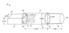
- a hollow dielectric pipe 16is coupled to the extended conductors (or ridges or transmission lines) 12 , 14 of a modified double ridge waveguide 10 to form an antenna 8 with a substantially plane wave substantially within a cross section of the dielectric pipe 16 .
- This guided wavemay be transmitted into free space by tapering the wall 18 thickness of the dielectric pipe 16 from a cross-section 20 towards a second end 22 of the dielectric pipe 16 . Adjacent to the second end 22 , the wave has maximum planarity and is substantially confined to a diameter that is substantially similar to the diameter of the dielectric pipe 16 .
- substantially plane wave conditionsare in a region about 0.75 inches in diameter for frequencies that range from about 5.6 GHz to about 16 GHz.
- the dimensions shown in FIG. 1are exemplary, and may be modified within the scope of the present invention. However, other suitable materials, and suitable geometries can also be used, and other suitable frequencies can also be achieved.
- the plane wave conditions and nearly uniform field distribution in the small regionis suited for measuring constitutive properties or the transmission and reflection coefficients of samples of sheet materials, particularly graded impedance cards.
- the first end 26 of the dielectric pipe 16is positioned to surround the extended conductors 12 , 14 .
- the dielectric pipe 16may be fixed to the waveguide 10 by any suitable means, such as a pressure fit or an adhesive.
- slotsare formed at the first end 26 of dielectric pipe 16 so that the slots may be positioned about the double ridge waveguide 10 .
- the dielectric pipe 16may then be fixed to (or inserted by) the waveguide 10 by any suitable means, such as a pressure fit or an adhesive.
- an unmodified double ridge waveguide 101has an upper ridge 12 ′ and a lower ridge 14 ′.
- the side walls 16 , 18 , the top wall 20 and the bottom wall 22are removed from an end 30 along a length of the double ridge waveguide 101 to form the modified double ridge wave guide 10 of FIGS. 1 and 2 with the extended conductors 12 , 14 .
- the extended conductors 12 , 14may be attached by any suitable means, such as welding, to an unmodified double ridge waveguide.
- the mouth 32 of the modified double ridge waveguide 10is an abrupt termination of the walls 16 , 18 , 20 , 22 of the double ridge waveguide 101 of FIG. 3 .
- the extended conductors 12 , 14continue beyond the mouth 32 .
- the resulting capacitive echo (from the termination of the top wall 20 and the bottom wall 22 ) and inductive echo (from the termination of the side walls 16 , 18 )substantially cancel each other, thus, making the transition from the double ridge waveguide 10 to a two-conductor transverse electromagnetic (TEM) line formed of the extended conductors 12 , 14 well matched.
- TEMtransverse electromagnetic
- TEM linescan be effectively coupled to dielectric slab waveguides by placing the TEM line and the dielectric slab in direct contact with each other (see the sununary article by Eric Spitz, “A class of new type of broad-band antennas”, in Electromagnetic Theory and Antennas, edited by E. C. Jordan, Pergamon Press, New York, 1963, pp. 1139-1148, expressly incorporated herein by reference in its entirety).
- the combined structurenominally supports several hybrid modes.
- the wave contained entirely in the TEM line at the beginning of the structuremay be substantially transferred to the dielectric slab after a coupling length.
- the efficiency of the transferis maximized when the wave on the TEM line and the surface wave on the dielectric waveguide have similar phase velocities.
- the dielectric pipeis suitable for coupling to the TEM line, because the lowest order linearly polarized mode supported by the dielectric pipe carries most of its energy in the air inside the dielectric pipe. Therefore, the phase velocity of the lower order linearly polarized mode in the dielectric pipe is close to the speed of light in air, as is the phase velocity of the TEM line.
- FIG. 4shows a vector plot of a calculated E-field inside the dielectric pipe as a broadband pulse propagates within it.
- the spectrum of the pulseis in a range from about 5.5 GHz to about 18 GHz. Because of symmetry, only one quadrant of the structure is shown. Overlaid on the vector plot are contours of strength of the principal (or dominant) vertically polarized field Ey.
- FIG. 5shows the calculated H-field vector plot and associated contours of field strength of the dominant horizontal magnetic field Hx.
- the field inside the pipeis dominated by a vertically polarized quasi-plane wave.
- the electromagnetic fieldis nearly uniform across the horizontal plane and varies by approximately 10% in the vertical plane, exhibiting a maximum at the center of the pipe. Outside the pipe the field decays exponentially, as expected from any guided surface wave.
- extended ridge lengthshould be close to a coupling length. This length can be determined utilizing full wave computational electromagnetic codes. To further optimize (or increase) this transfer, the echo from the ridge termination may be minimized (or reduced).
- this minimizationmay be accomplished by removing a portion (or forming a notch) 60 , 62 of the extended conductors 12 , 16 towards the dielectric pipe 16 to form destructive interference between the first portion 60 and the second portion 62 .
- the dielectric pipe 16must be terminated with minimum reflection.
- reflectionis minimized by linearly tapering the wall thickness 18 of the dielectric pipe 16 .
- FIG. 7shows the computed and measured reflection coefficient at a plane just before the end of the waveguide for an antenna of an embodiment of the present invention.
- the measurementwas performed utilizing an Agilent 8720 vector network analyzer.
- a time domain gatewas utilized to eliminate the SMA coax to waveguide transition of the waveguide feed from the measurement to measure only the radiating portion of the antenna.
- the coax to waveguide transition of commercially available double ridge waveguidestypically exhibits a reflection coefficient greater than ⁇ 10 dB from 6.5 GHz to 16 GHz.
- FIG. 7shows that the antenna radiates at least half the power fed to it at 6 GHz ( ⁇ 3 dB reflection coefficient) and greater than 90% of the power above 7.5 GHz ( ⁇ 10 dB reflection coefficient).
- FIG. 8shows experimentally determined spot-size as a function of frequency of an antenna of an embodiment of the present invention, as observed 0.5 inches from its end.
- a pair of aligned antennaswere moved across a resistive sheet (R-card) with an insertion loss of about ⁇ 1.8 dB, so that as the R-card crosses the midplane of the antennas, the R-card interrupts the signal propagating between the antennas.
- R-cardresistive sheet
- the measured insertion losswas plotted (y axis) versus the position of the probes relative to the edge of the R-card from 3 inches away (where ⁇ 3 inches is not interrupting the beam) to 3 inches past the center of the beam (where +3 inches is fully interrupting the beam).
- the point at which the antennas register half the lossmay be used as a gauge of the size and shape of the antenna's spot-size. As in FIG. 8 , this 50% error region occurs just as the center of the antennas' beam crosses half an inch into the R-card. This boundary is nearly frequency independent (x axis) from 5.4 GHz through 16 GHz.
- An exemplary applicationis a measurement of resistively loaded sheet goods, where the local value of the sheet conductance (or loss) is assessed as a function of position.
- a small spot-size and operation over a broadband of frequenciesis desirable.
- the spot-size shown in FIG. 8is exemplary. For typical samples, 50% of the value is registered within approximately half an inch of the edge of the material and 90% of the value is registered within approximately 1.5 inches, implying a spot-size containing 90% of the energy in the beam in about a 3 inch diameter.
- the removal of portions (or the formed notches) 60 , 62 from the ridge extension 12 , 14 , as shown in FIG. 6may be modified by a series of cuts, following the practice of multi-section transformers, to obtain a wider frequency match.
- the dielectric constant of a material of a dielectric pipe of the present inventionwas about 2.9, but other suitable materials with other suitable dielectric constants may be utilized.
- the dielectric constants of the dielectric pipemay range from about 2.5 to about 3.5, but other suitable dielectric constants could also be utilized.
- the wall thickness and diameter of the dielectric pipewould be adjusted accordingly, as may be determined by one skilled in the art.
- an embodiment of the present inventionprovides a waveguide that includes: a first section 10 including a first surface facing a flange 200 , a second surface oppositely facing away from the first surface, an upper wall 20 , and a lower wall 22 facing the upper wall; and a second section 12 , 14 extending out from the second surface; wherein the first section 10 includes an upper ridge 12 ′ disposed on the upper wall 20 of the first section 10 and a lower ridge 14 ′ disposed on the lower wall 22 of the first section 10 , wherein the second section 12 , 14 includes an upper conductor 12 extending out from a top portion of the second surface and a lower conductor 14 extending out from a lower portion of the second surface with a gap between the upper conductor 12 and the lower conductor 14 , wherein the upper conductor 12 is electrically connected to the upper ridge 12 ′, wherein the lower conductor 14 is electrically connected to the lower ridge 14 ′, and wherein the upper conductor 12 and the
- the upper conductor 12may include an upper notch 60 at a distal end away from the second surface, wherein the lower conductor 14 may include a lower notch 62 at a distal end away from the second surface, and wherein the upper and lower notches 60 , 62 are configured to reduce reflection of the wave propagated by the upper conductor 12 and the lower conductor 14 .
- the second sectionmay consist essentially of the upper conductor 12 extending out from the top portion of the second surface and the lower conductor 14 extending out from the lower portion of the second surface with the gap between the upper conductor 12 and the lower conductor 14 .
- an embodiment of the present inventionprovides a waveguide including: a double-ridged waveguide section 10 having a first ridge 12 ′ and a second ridge 14 ′; a first conductor 12 extending from the first ridge 12 ′; and a second conductor 14 extending from the second ridge 14 ′; wherein the first and second conductors 12 , 14 are configured to propagate a wave from the double-ridged waveguide section 10 and to reduce a discontinuity of the wave propagated at a connection between the double-ridged waveguide section 10 and the two conductors 12 , 14 .
- an embodiment of the present inventionprovides a dielectric pipe antenna including: a dielectric pipe 16 ; and a waveguide 10 for receiving one end of the dielectric pipe 16 ; wherein the waveguide 10 includes: a first section 10 including a first surface facing a flange, a second surface oppositely facing away from the first surface, an upper wall 20 , and a lower wall 22 facing the upper wall 20 ; and a second section 12 , 14 extending out from the second surface; wherein the first section 10 includes an upper ridge 12 ′ disposed on the upper wall of the first section 10 and a lower ridge 14 ′ disposed on the lower wall of the first section 10 , wherein the second section 12 , 14 includes an upper conductor 12 extending out from a top portion of the second surface and a lower conductor 14 extending out from a lower portion of the second surface with a gap between the upper conductor 12 and the lower conductor 14 , and wherein the dielectric pipe 16 includes: a hollow tubular dielectric
- the dielectric pipe 16may have a dielectric constant ranging from about 1.5 to about 9, or the dielectric pipe 16 may have a dielectric constant ranging from about 2.5 to about 3.
- hollow tubular dielectric sleeve portion 17may surround and be electromagnetically coupled to the upper conductor and the lower conductor of the second section.
- a wave generated within the dielectric pipe 16may be substantially planar, and wherein a generated wave upon exiting the dielectric pipe 16 may be substantially the same as the wave generated within the dielectric pipe 16 surrounding the upper conductor 12 and the lower conductor 14 .
- each of the upper conductor 12 and the lower conductor 14 of the second section 12 , 14may have a length configured to maximize an electromagnetic coupling of the upper conductor 12 and the lower conductor 14 to the dielectric pipe 16 surrounding the upper conductor 12 and the lower conductor 14 .
- the upper conductor 12may include an upper notch 60 at a distal end away from the second surface, wherein the lower conductor 12 may include a lower notch 62 at a distal end away from the second surface, and wherein the upper and lower notches 60 , 62 may be configured to reduce reflection of the wave propagated by the upper conductor 12 and the lower conductor 14 .
- a height of the first metallic section 10 of the waveguidemay be about 0.473 inches, a width of the first metallic section 10 of the waveguide may be about 0.833 inches, and each of the upper conductor 12 and the lower conductor 14 may have a length of about 1.476 inches, and wherein the height of the first metallic section 10 , the width of the first metallic section 10 , and the length of each of the upper conductor 12 and the lower conductor 14 may be configured to operate at frequency ranging from about 5.5 GHz to about 18 GHz.
- a length of the hollow tubular dielectric sleeve 17may be at about 2.952 inches, the internal sleeve diameter may be about 0.886 inches and a length of the tapered dielectric pipe portion 18 may be at about 1.969 in, and wherein the length of the hollow tubular dielectric sleeve 17 , the internal sleeve diameter, and the length of the tapered dielectric pipe portion 18 may be configured to operate at a frequency range of about 5.5 GHz to about 18 GHz.
- a length of the hollow tubular dielectric sleeve 17 , the internal sleeve diameter, a length of the tapered dielectric pipe portion 18 and proportions of the double-ridged waveguide 10may be configured to operate at a frequency range of about 100 MHz to about 100 GHz.
- the one end of the dielectric pipe 16may make a releasable-fit engagement with the second metallic section of the waveguide.
- an embodiment of the present inventionprovides a hollow dielectric pipe polyrod antenna capable of providing a relatively small spot-size in a plane wave condition.
Landscapes
- Waveguide Aerials (AREA)
Abstract
Description
Claims (15)
Priority Applications (1)
| Application Number | Priority Date | Filing Date | Title |
|---|---|---|---|
| US12/004,729US7786946B2 (en) | 2006-12-22 | 2007-12-21 | Hollow dielectric pipe polyrod antenna |
Applications Claiming Priority (2)
| Application Number | Priority Date | Filing Date | Title |
|---|---|---|---|
| US87153606P | 2006-12-22 | 2006-12-22 | |
| US12/004,729US7786946B2 (en) | 2006-12-22 | 2007-12-21 | Hollow dielectric pipe polyrod antenna |
Publications (2)
| Publication Number | Publication Date |
|---|---|
| US20090160721A1 US20090160721A1 (en) | 2009-06-25 |
| US7786946B2true US7786946B2 (en) | 2010-08-31 |
Family
ID=40787964
Family Applications (1)
| Application Number | Title | Priority Date | Filing Date |
|---|---|---|---|
| US12/004,729Expired - Fee RelatedUS7786946B2 (en) | 2006-12-22 | 2007-12-21 | Hollow dielectric pipe polyrod antenna |
Country Status (1)
| Country | Link |
|---|---|
| US (1) | US7786946B2 (en) |
Cited By (167)
| Publication number | Priority date | Publication date | Assignee | Title |
|---|---|---|---|---|
| US9119127B1 (en) | 2012-12-05 | 2015-08-25 | At&T Intellectual Property I, Lp | Backhaul link for distributed antenna system |
| US9154966B2 (en) | 2013-11-06 | 2015-10-06 | At&T Intellectual Property I, Lp | Surface-wave communications and methods thereof |
| US9209902B2 (en) | 2013-12-10 | 2015-12-08 | At&T Intellectual Property I, L.P. | Quasi-optical coupler |
| US9312919B1 (en) | 2014-10-21 | 2016-04-12 | At&T Intellectual Property I, Lp | Transmission device with impairment compensation and methods for use therewith |
| US9461706B1 (en) | 2015-07-31 | 2016-10-04 | At&T Intellectual Property I, Lp | Method and apparatus for exchanging communication signals |
| US9490869B1 (en) | 2015-05-14 | 2016-11-08 | At&T Intellectual Property I, L.P. | Transmission medium having multiple cores and methods for use therewith |
| US9503189B2 (en) | 2014-10-10 | 2016-11-22 | At&T Intellectual Property I, L.P. | Method and apparatus for arranging communication sessions in a communication system |
| US9509415B1 (en) | 2015-06-25 | 2016-11-29 | At&T Intellectual Property I, L.P. | Methods and apparatus for inducing a fundamental wave mode on a transmission medium |
| US9520945B2 (en) | 2014-10-21 | 2016-12-13 | At&T Intellectual Property I, L.P. | Apparatus for providing communication services and methods thereof |
| US9525524B2 (en) | 2013-05-31 | 2016-12-20 | At&T Intellectual Property I, L.P. | Remote distributed antenna system |
| US9525210B2 (en) | 2014-10-21 | 2016-12-20 | At&T Intellectual Property I, L.P. | Guided-wave transmission device with non-fundamental mode propagation and methods for use therewith |
| US9531427B2 (en) | 2014-11-20 | 2016-12-27 | At&T Intellectual Property I, L.P. | Transmission device with mode division multiplexing and methods for use therewith |
| US9564947B2 (en) | 2014-10-21 | 2017-02-07 | At&T Intellectual Property I, L.P. | Guided-wave transmission device with diversity and methods for use therewith |
| US9577306B2 (en) | 2014-10-21 | 2017-02-21 | At&T Intellectual Property I, L.P. | Guided-wave transmission device and methods for use therewith |
| US9608692B2 (en) | 2015-06-11 | 2017-03-28 | At&T Intellectual Property I, L.P. | Repeater and methods for use therewith |
| US9608740B2 (en) | 2015-07-15 | 2017-03-28 | At&T Intellectual Property I, L.P. | Method and apparatus for launching a wave mode that mitigates interference |
| US9615269B2 (en) | 2014-10-02 | 2017-04-04 | At&T Intellectual Property I, L.P. | Method and apparatus that provides fault tolerance in a communication network |
| US9628116B2 (en) | 2015-07-14 | 2017-04-18 | At&T Intellectual Property I, L.P. | Apparatus and methods for transmitting wireless signals |
| US9628854B2 (en) | 2014-09-29 | 2017-04-18 | At&T Intellectual Property I, L.P. | Method and apparatus for distributing content in a communication network |
| US9640850B2 (en) | 2015-06-25 | 2017-05-02 | At&T Intellectual Property I, L.P. | Methods and apparatus for inducing a non-fundamental wave mode on a transmission medium |
| US9653770B2 (en) | 2014-10-21 | 2017-05-16 | At&T Intellectual Property I, L.P. | Guided wave coupler, coupling module and methods for use therewith |
| US9654173B2 (en) | 2014-11-20 | 2017-05-16 | At&T Intellectual Property I, L.P. | Apparatus for powering a communication device and methods thereof |
| US9667317B2 (en) | 2015-06-15 | 2017-05-30 | At&T Intellectual Property I, L.P. | Method and apparatus for providing security using network traffic adjustments |
| US9680670B2 (en) | 2014-11-20 | 2017-06-13 | At&T Intellectual Property I, L.P. | Transmission device with channel equalization and control and methods for use therewith |
| US9685992B2 (en) | 2014-10-03 | 2017-06-20 | At&T Intellectual Property I, L.P. | Circuit panel network and methods thereof |
| US9692101B2 (en) | 2014-08-26 | 2017-06-27 | At&T Intellectual Property I, L.P. | Guided wave couplers for coupling electromagnetic waves between a waveguide surface and a surface of a wire |
| US9705571B2 (en) | 2015-09-16 | 2017-07-11 | At&T Intellectual Property I, L.P. | Method and apparatus for use with a radio distributed antenna system |
| US9705561B2 (en) | 2015-04-24 | 2017-07-11 | At&T Intellectual Property I, L.P. | Directional coupling device and methods for use therewith |
| US9722318B2 (en) | 2015-07-14 | 2017-08-01 | At&T Intellectual Property I, L.P. | Method and apparatus for coupling an antenna to a device |
| US9729197B2 (en) | 2015-10-01 | 2017-08-08 | At&T Intellectual Property I, L.P. | Method and apparatus for communicating network management traffic over a network |
| US9735833B2 (en) | 2015-07-31 | 2017-08-15 | At&T Intellectual Property I, L.P. | Method and apparatus for communications management in a neighborhood network |
| US9742462B2 (en) | 2014-12-04 | 2017-08-22 | At&T Intellectual Property I, L.P. | Transmission medium and communication interfaces and methods for use therewith |
| US9748626B2 (en) | 2015-05-14 | 2017-08-29 | At&T Intellectual Property I, L.P. | Plurality of cables having different cross-sectional shapes which are bundled together to form a transmission medium |
| US9749053B2 (en) | 2015-07-23 | 2017-08-29 | At&T Intellectual Property I, L.P. | Node device, repeater and methods for use therewith |
| US9749013B2 (en) | 2015-03-17 | 2017-08-29 | At&T Intellectual Property I, L.P. | Method and apparatus for reducing attenuation of electromagnetic waves guided by a transmission medium |
| US9755697B2 (en) | 2014-09-15 | 2017-09-05 | At&T Intellectual Property I, L.P. | Method and apparatus for sensing a condition in a transmission medium of electromagnetic waves |
| US9762289B2 (en) | 2014-10-14 | 2017-09-12 | At&T Intellectual Property I, L.P. | Method and apparatus for transmitting or receiving signals in a transportation system |
| US9769020B2 (en) | 2014-10-21 | 2017-09-19 | At&T Intellectual Property I, L.P. | Method and apparatus for responding to events affecting communications in a communication network |
| US9769128B2 (en) | 2015-09-28 | 2017-09-19 | At&T Intellectual Property I, L.P. | Method and apparatus for encryption of communications over a network |
| US9780834B2 (en) | 2014-10-21 | 2017-10-03 | At&T Intellectual Property I, L.P. | Method and apparatus for transmitting electromagnetic waves |
| US9793954B2 (en) | 2015-04-28 | 2017-10-17 | At&T Intellectual Property I, L.P. | Magnetic coupling device and methods for use therewith |
| US9793951B2 (en) | 2015-07-15 | 2017-10-17 | At&T Intellectual Property I, L.P. | Method and apparatus for launching a wave mode that mitigates interference |
| US9793955B2 (en) | 2015-04-24 | 2017-10-17 | At&T Intellectual Property I, Lp | Passive electrical coupling device and methods for use therewith |
| US9800327B2 (en) | 2014-11-20 | 2017-10-24 | At&T Intellectual Property I, L.P. | Apparatus for controlling operations of a communication device and methods thereof |
| US9820146B2 (en) | 2015-06-12 | 2017-11-14 | At&T Intellectual Property I, L.P. | Method and apparatus for authentication and identity management of communicating devices |
| US9836957B2 (en) | 2015-07-14 | 2017-12-05 | At&T Intellectual Property I, L.P. | Method and apparatus for communicating with premises equipment |
| US9838896B1 (en) | 2016-12-09 | 2017-12-05 | At&T Intellectual Property I, L.P. | Method and apparatus for assessing network coverage |
| US9847566B2 (en) | 2015-07-14 | 2017-12-19 | At&T Intellectual Property I, L.P. | Method and apparatus for adjusting a field of a signal to mitigate interference |
| US9847850B2 (en) | 2014-10-14 | 2017-12-19 | At&T Intellectual Property I, L.P. | Method and apparatus for adjusting a mode of communication in a communication network |
| US9853342B2 (en) | 2015-07-14 | 2017-12-26 | At&T Intellectual Property I, L.P. | Dielectric transmission medium connector and methods for use therewith |
| US9860075B1 (en) | 2016-08-26 | 2018-01-02 | At&T Intellectual Property I, L.P. | Method and communication node for broadband distribution |
| US9866309B2 (en) | 2015-06-03 | 2018-01-09 | At&T Intellectual Property I, Lp | Host node device and methods for use therewith |
| US9865911B2 (en) | 2015-06-25 | 2018-01-09 | At&T Intellectual Property I, L.P. | Waveguide system for slot radiating first electromagnetic waves that are combined into a non-fundamental wave mode second electromagnetic wave on a transmission medium |
| US9871283B2 (en) | 2015-07-23 | 2018-01-16 | At&T Intellectual Property I, Lp | Transmission medium having a dielectric core comprised of plural members connected by a ball and socket configuration |
| US9871282B2 (en) | 2015-05-14 | 2018-01-16 | At&T Intellectual Property I, L.P. | At least one transmission medium having a dielectric surface that is covered at least in part by a second dielectric |
| US9876571B2 (en) | 2015-02-20 | 2018-01-23 | At&T Intellectual Property I, Lp | Guided-wave transmission device with non-fundamental mode propagation and methods for use therewith |
| US9876264B2 (en) | 2015-10-02 | 2018-01-23 | At&T Intellectual Property I, Lp | Communication system, guided wave switch and methods for use therewith |
| US9876605B1 (en) | 2016-10-21 | 2018-01-23 | At&T Intellectual Property I, L.P. | Launcher and coupling system to support desired guided wave mode |
| US9882277B2 (en) | 2015-10-02 | 2018-01-30 | At&T Intellectual Property I, Lp | Communication device and antenna assembly with actuated gimbal mount |
| US9882257B2 (en) | 2015-07-14 | 2018-01-30 | At&T Intellectual Property I, L.P. | Method and apparatus for launching a wave mode that mitigates interference |
| US9893795B1 (en) | 2016-12-07 | 2018-02-13 | At&T Intellectual Property I, Lp | Method and repeater for broadband distribution |
| US9906269B2 (en) | 2014-09-17 | 2018-02-27 | At&T Intellectual Property I, L.P. | Monitoring and mitigating conditions in a communication network |
| US9904535B2 (en) | 2015-09-14 | 2018-02-27 | At&T Intellectual Property I, L.P. | Method and apparatus for distributing software |
| US9912381B2 (en) | 2015-06-03 | 2018-03-06 | At&T Intellectual Property I, Lp | Network termination and methods for use therewith |
| US9912419B1 (en) | 2016-08-24 | 2018-03-06 | At&T Intellectual Property I, L.P. | Method and apparatus for managing a fault in a distributed antenna system |
| US9912027B2 (en) | 2015-07-23 | 2018-03-06 | At&T Intellectual Property I, L.P. | Method and apparatus for exchanging communication signals |
| US9913139B2 (en) | 2015-06-09 | 2018-03-06 | At&T Intellectual Property I, L.P. | Signal fingerprinting for authentication of communicating devices |
| US9911020B1 (en) | 2016-12-08 | 2018-03-06 | At&T Intellectual Property I, L.P. | Method and apparatus for tracking via a radio frequency identification device |
| US9917341B2 (en) | 2015-05-27 | 2018-03-13 | At&T Intellectual Property I, L.P. | Apparatus and method for launching electromagnetic waves and for modifying radial dimensions of the propagating electromagnetic waves |
| US9927517B1 (en) | 2016-12-06 | 2018-03-27 | At&T Intellectual Property I, L.P. | Apparatus and methods for sensing rainfall |
| US9948333B2 (en) | 2015-07-23 | 2018-04-17 | At&T Intellectual Property I, L.P. | Method and apparatus for wireless communications to mitigate interference |
| US9948354B2 (en) | 2015-04-28 | 2018-04-17 | At&T Intellectual Property I, L.P. | Magnetic coupling device with reflective plate and methods for use therewith |
| US9954287B2 (en) | 2014-11-20 | 2018-04-24 | At&T Intellectual Property I, L.P. | Apparatus for converting wireless signals and electromagnetic waves and methods thereof |
| US9967173B2 (en) | 2015-07-31 | 2018-05-08 | At&T Intellectual Property I, L.P. | Method and apparatus for authentication and identity management of communicating devices |
| US9973940B1 (en) | 2017-02-27 | 2018-05-15 | At&T Intellectual Property I, L.P. | Apparatus and methods for dynamic impedance matching of a guided wave launcher |
| US9991580B2 (en) | 2016-10-21 | 2018-06-05 | At&T Intellectual Property I, L.P. | Launcher and coupling system for guided wave mode cancellation |
| US9999038B2 (en) | 2013-05-31 | 2018-06-12 | At&T Intellectual Property I, L.P. | Remote distributed antenna system |
| US9998870B1 (en) | 2016-12-08 | 2018-06-12 | At&T Intellectual Property I, L.P. | Method and apparatus for proximity sensing |
| US9997819B2 (en) | 2015-06-09 | 2018-06-12 | At&T Intellectual Property I, L.P. | Transmission medium and method for facilitating propagation of electromagnetic waves via a core |
| US10009901B2 (en) | 2015-09-16 | 2018-06-26 | At&T Intellectual Property I, L.P. | Method, apparatus, and computer-readable storage medium for managing utilization of wireless resources between base stations |
| US10009067B2 (en) | 2014-12-04 | 2018-06-26 | At&T Intellectual Property I, L.P. | Method and apparatus for configuring a communication interface |
| US10009063B2 (en) | 2015-09-16 | 2018-06-26 | At&T Intellectual Property I, L.P. | Method and apparatus for use with a radio distributed antenna system having an out-of-band reference signal |
| US10009065B2 (en) | 2012-12-05 | 2018-06-26 | At&T Intellectual Property I, L.P. | Backhaul link for distributed antenna system |
| US10020587B2 (en) | 2015-07-31 | 2018-07-10 | At&T Intellectual Property I, L.P. | Radial antenna and methods for use therewith |
| US10020844B2 (en) | 2016-12-06 | 2018-07-10 | T&T Intellectual Property I, L.P. | Method and apparatus for broadcast communication via guided waves |
| US10027397B2 (en) | 2016-12-07 | 2018-07-17 | At&T Intellectual Property I, L.P. | Distributed antenna system and methods for use therewith |
| US10033108B2 (en) | 2015-07-14 | 2018-07-24 | At&T Intellectual Property I, L.P. | Apparatus and methods for generating an electromagnetic wave having a wave mode that mitigates interference |
| US10033107B2 (en) | 2015-07-14 | 2018-07-24 | At&T Intellectual Property I, L.P. | Method and apparatus for coupling an antenna to a device |
| US10044409B2 (en) | 2015-07-14 | 2018-08-07 | At&T Intellectual Property I, L.P. | Transmission medium and methods for use therewith |
| US10051483B2 (en) | 2015-10-16 | 2018-08-14 | At&T Intellectual Property I, L.P. | Method and apparatus for directing wireless signals |
| US10051629B2 (en) | 2015-09-16 | 2018-08-14 | At&T Intellectual Property I, L.P. | Method and apparatus for use with a radio distributed antenna system having an in-band reference signal |
| US10069535B2 (en) | 2016-12-08 | 2018-09-04 | At&T Intellectual Property I, L.P. | Apparatus and methods for launching electromagnetic waves having a certain electric field structure |
| US10074890B2 (en) | 2015-10-02 | 2018-09-11 | At&T Intellectual Property I, L.P. | Communication device and antenna with integrated light assembly |
| US10079661B2 (en) | 2015-09-16 | 2018-09-18 | At&T Intellectual Property I, L.P. | Method and apparatus for use with a radio distributed antenna system having a clock reference |
| US10090594B2 (en) | 2016-11-23 | 2018-10-02 | At&T Intellectual Property I, L.P. | Antenna system having structural configurations for assembly |
| US10090606B2 (en) | 2015-07-15 | 2018-10-02 | At&T Intellectual Property I, L.P. | Antenna system with dielectric array and methods for use therewith |
| US10103801B2 (en) | 2015-06-03 | 2018-10-16 | At&T Intellectual Property I, L.P. | Host node device and methods for use therewith |
| US10103422B2 (en) | 2016-12-08 | 2018-10-16 | At&T Intellectual Property I, L.P. | Method and apparatus for mounting network devices |
| US10135145B2 (en) | 2016-12-06 | 2018-11-20 | At&T Intellectual Property I, L.P. | Apparatus and methods for generating an electromagnetic wave along a transmission medium |
| US10135147B2 (en) | 2016-10-18 | 2018-11-20 | At&T Intellectual Property I, L.P. | Apparatus and methods for launching guided waves via an antenna |
| US10135146B2 (en) | 2016-10-18 | 2018-11-20 | At&T Intellectual Property I, L.P. | Apparatus and methods for launching guided waves via circuits |
| US10136434B2 (en) | 2015-09-16 | 2018-11-20 | At&T Intellectual Property I, L.P. | Method and apparatus for use with a radio distributed antenna system having an ultra-wideband control channel |
| US10139820B2 (en) | 2016-12-07 | 2018-11-27 | At&T Intellectual Property I, L.P. | Method and apparatus for deploying equipment of a communication system |
| US10142086B2 (en) | 2015-06-11 | 2018-11-27 | At&T Intellectual Property I, L.P. | Repeater and methods for use therewith |
| US10148016B2 (en) | 2015-07-14 | 2018-12-04 | At&T Intellectual Property I, L.P. | Apparatus and methods for communicating utilizing an antenna array |
| US10144036B2 (en) | 2015-01-30 | 2018-12-04 | At&T Intellectual Property I, L.P. | Method and apparatus for mitigating interference affecting a propagation of electromagnetic waves guided by a transmission medium |
| US10154493B2 (en) | 2015-06-03 | 2018-12-11 | At&T Intellectual Property I, L.P. | Network termination and methods for use therewith |
| US10170840B2 (en) | 2015-07-14 | 2019-01-01 | At&T Intellectual Property I, L.P. | Apparatus and methods for sending or receiving electromagnetic signals |
| US10168695B2 (en) | 2016-12-07 | 2019-01-01 | At&T Intellectual Property I, L.P. | Method and apparatus for controlling an unmanned aircraft |
| US10178445B2 (en) | 2016-11-23 | 2019-01-08 | At&T Intellectual Property I, L.P. | Methods, devices, and systems for load balancing between a plurality of waveguides |
| US10205655B2 (en) | 2015-07-14 | 2019-02-12 | At&T Intellectual Property I, L.P. | Apparatus and methods for communicating utilizing an antenna array and multiple communication paths |
| US10224634B2 (en) | 2016-11-03 | 2019-03-05 | At&T Intellectual Property I, L.P. | Methods and apparatus for adjusting an operational characteristic of an antenna |
| US10225025B2 (en) | 2016-11-03 | 2019-03-05 | At&T Intellectual Property I, L.P. | Method and apparatus for detecting a fault in a communication system |
| US10243270B2 (en) | 2016-12-07 | 2019-03-26 | At&T Intellectual Property I, L.P. | Beam adaptive multi-feed dielectric antenna system and methods for use therewith |
| US10243784B2 (en) | 2014-11-20 | 2019-03-26 | At&T Intellectual Property I, L.P. | System for generating topology information and methods thereof |
| US10264586B2 (en) | 2016-12-09 | 2019-04-16 | At&T Mobility Ii Llc | Cloud-based packet controller and methods for use therewith |
| US10291311B2 (en) | 2016-09-09 | 2019-05-14 | At&T Intellectual Property I, L.P. | Method and apparatus for mitigating a fault in a distributed antenna system |
| US10291334B2 (en) | 2016-11-03 | 2019-05-14 | At&T Intellectual Property I, L.P. | System for detecting a fault in a communication system |
| US10298293B2 (en) | 2017-03-13 | 2019-05-21 | At&T Intellectual Property I, L.P. | Apparatus of communication utilizing wireless network devices |
| US10305190B2 (en) | 2016-12-01 | 2019-05-28 | At&T Intellectual Property I, L.P. | Reflecting dielectric antenna system and methods for use therewith |
| US10312567B2 (en) | 2016-10-26 | 2019-06-04 | At&T Intellectual Property I, L.P. | Launcher with planar strip antenna and methods for use therewith |
| US10320586B2 (en) | 2015-07-14 | 2019-06-11 | At&T Intellectual Property I, L.P. | Apparatus and methods for generating non-interfering electromagnetic waves on an insulated transmission medium |
| US10326689B2 (en) | 2016-12-08 | 2019-06-18 | At&T Intellectual Property I, L.P. | Method and system for providing alternative communication paths |
| US10326494B2 (en) | 2016-12-06 | 2019-06-18 | At&T Intellectual Property I, L.P. | Apparatus for measurement de-embedding and methods for use therewith |
| US10332553B1 (en) | 2017-12-29 | 2019-06-25 | Headway Technologies, Inc. | Double ridge near-field transducers |
| US10340603B2 (en) | 2016-11-23 | 2019-07-02 | At&T Intellectual Property I, L.P. | Antenna system having shielded structural configurations for assembly |
| US10340983B2 (en) | 2016-12-09 | 2019-07-02 | At&T Intellectual Property I, L.P. | Method and apparatus for surveying remote sites via guided wave communications |
| US10341142B2 (en) | 2015-07-14 | 2019-07-02 | At&T Intellectual Property I, L.P. | Apparatus and methods for generating non-interfering electromagnetic waves on an uninsulated conductor |
| US10340573B2 (en) | 2016-10-26 | 2019-07-02 | At&T Intellectual Property I, L.P. | Launcher with cylindrical coupling device and methods for use therewith |
| US10340600B2 (en) | 2016-10-18 | 2019-07-02 | At&T Intellectual Property I, L.P. | Apparatus and methods for launching guided waves via plural waveguide systems |
| US10340601B2 (en) | 2016-11-23 | 2019-07-02 | At&T Intellectual Property I, L.P. | Multi-antenna system and methods for use therewith |
| US10348391B2 (en) | 2015-06-03 | 2019-07-09 | At&T Intellectual Property I, L.P. | Client node device with frequency conversion and methods for use therewith |
| US10355367B2 (en) | 2015-10-16 | 2019-07-16 | At&T Intellectual Property I, L.P. | Antenna structure for exchanging wireless signals |
| US10361489B2 (en) | 2016-12-01 | 2019-07-23 | At&T Intellectual Property I, L.P. | Dielectric dish antenna system and methods for use therewith |
| US10359749B2 (en) | 2016-12-07 | 2019-07-23 | At&T Intellectual Property I, L.P. | Method and apparatus for utilities management via guided wave communication |
| US10374316B2 (en) | 2016-10-21 | 2019-08-06 | At&T Intellectual Property I, L.P. | System and dielectric antenna with non-uniform dielectric |
| US10382976B2 (en) | 2016-12-06 | 2019-08-13 | At&T Intellectual Property I, L.P. | Method and apparatus for managing wireless communications based on communication paths and network device positions |
| US10389029B2 (en) | 2016-12-07 | 2019-08-20 | At&T Intellectual Property I, L.P. | Multi-feed dielectric antenna system with core selection and methods for use therewith |
| US10389037B2 (en) | 2016-12-08 | 2019-08-20 | At&T Intellectual Property I, L.P. | Apparatus and methods for selecting sections of an antenna array and use therewith |
| US10396887B2 (en) | 2015-06-03 | 2019-08-27 | At&T Intellectual Property I, L.P. | Client node device and methods for use therewith |
| US10411356B2 (en) | 2016-12-08 | 2019-09-10 | At&T Intellectual Property I, L.P. | Apparatus and methods for selectively targeting communication devices with an antenna array |
| US10439675B2 (en) | 2016-12-06 | 2019-10-08 | At&T Intellectual Property I, L.P. | Method and apparatus for repeating guided wave communication signals |
| US10446936B2 (en) | 2016-12-07 | 2019-10-15 | At&T Intellectual Property I, L.P. | Multi-feed dielectric antenna system and methods for use therewith |
| US10498044B2 (en) | 2016-11-03 | 2019-12-03 | At&T Intellectual Property I, L.P. | Apparatus for configuring a surface of an antenna |
| US10530505B2 (en) | 2016-12-08 | 2020-01-07 | At&T Intellectual Property I, L.P. | Apparatus and methods for launching electromagnetic waves along a transmission medium |
| US10535928B2 (en) | 2016-11-23 | 2020-01-14 | At&T Intellectual Property I, L.P. | Antenna system and methods for use therewith |
| US10547348B2 (en) | 2016-12-07 | 2020-01-28 | At&T Intellectual Property I, L.P. | Method and apparatus for switching transmission mediums in a communication system |
| US10601494B2 (en) | 2016-12-08 | 2020-03-24 | At&T Intellectual Property I, L.P. | Dual-band communication device and method for use therewith |
| US10637149B2 (en) | 2016-12-06 | 2020-04-28 | At&T Intellectual Property I, L.P. | Injection molded dielectric antenna and methods for use therewith |
| US10644395B2 (en) | 2018-05-14 | 2020-05-05 | Freefall Aerospace, Inc. | Dielectric antenna array and system |
| US10650940B2 (en) | 2015-05-15 | 2020-05-12 | At&T Intellectual Property I, L.P. | Transmission medium having a conductive material and methods for use therewith |
| US10665942B2 (en) | 2015-10-16 | 2020-05-26 | At&T Intellectual Property I, L.P. | Method and apparatus for adjusting wireless communications |
| US10679767B2 (en) | 2015-05-15 | 2020-06-09 | At&T Intellectual Property I, L.P. | Transmission medium having a conductive material and methods for use therewith |
| US10694379B2 (en) | 2016-12-06 | 2020-06-23 | At&T Intellectual Property I, L.P. | Waveguide system with device-based authentication and methods for use therewith |
| US10714834B2 (en) | 2016-12-20 | 2020-07-14 | Arizona Board of Regents on behalf of Arlzona State University | Broadband quad-ridge horn antennas |
| US10727599B2 (en) | 2016-12-06 | 2020-07-28 | At&T Intellectual Property I, L.P. | Launcher with slot antenna and methods for use therewith |
| US10755542B2 (en) | 2016-12-06 | 2020-08-25 | At&T Intellectual Property I, L.P. | Method and apparatus for surveillance via guided wave communication |
| US10777879B2 (en) | 2017-07-24 | 2020-09-15 | Arizona Board Of Regents On Behalf Of Arizona State University | Optimal permeable antenna flux channels for conformal applications |
| US10777873B2 (en) | 2016-12-08 | 2020-09-15 | At&T Intellectual Property I, L.P. | Method and apparatus for mounting network devices |
| US10784670B2 (en) | 2015-07-23 | 2020-09-22 | At&T Intellectual Property I, L.P. | Antenna support for aligning an antenna |
| US10811767B2 (en) | 2016-10-21 | 2020-10-20 | At&T Intellectual Property I, L.P. | System and dielectric antenna with convex dielectric radome |
| US10819035B2 (en) | 2016-12-06 | 2020-10-27 | At&T Intellectual Property I, L.P. | Launcher with helical antenna and methods for use therewith |
| US10916969B2 (en) | 2016-12-08 | 2021-02-09 | At&T Intellectual Property I, L.P. | Method and apparatus for providing power using an inductive coupling |
| US10938108B2 (en) | 2016-12-08 | 2021-03-02 | At&T Intellectual Property I, L.P. | Frequency selective multi-feed dielectric antenna system and methods for use therewith |
| US11032819B2 (en) | 2016-09-15 | 2021-06-08 | At&T Intellectual Property I, L.P. | Method and apparatus for use with a radio distributed antenna system having a control channel reference signal |
| US11387560B2 (en) | 2019-12-03 | 2022-07-12 | At&T Intellectual Property I, L.P. | Impedance matched launcher with cylindrical coupling device and methods for use therewith |
| EP4481947A1 (en)* | 2023-06-20 | 2024-12-25 | Rohde & Schwarz GmbH & Co. KG | Metallic waveguide antenna |
Citations (9)
| Publication number | Priority date | Publication date | Assignee | Title |
|---|---|---|---|---|
| US3216017A (en)* | 1962-12-04 | 1965-11-02 | Martin Marietta Corp | Polarizer for use in antenna and transmission line systems |
| US3389394A (en)* | 1965-11-26 | 1968-06-18 | Radiation Inc | Multiple frequency antenna |
| US3518691A (en)* | 1968-04-23 | 1970-06-30 | Us Navy | Transition structure for broadband coupling of dielectric rod antenna to coaxial feed |
| US4468672A (en)* | 1981-10-28 | 1984-08-28 | Bell Telephone Laboratories, Incorporated | Wide bandwidth hybrid mode feeds |
| US4673945A (en)* | 1984-09-24 | 1987-06-16 | Alpha Industries, Inc. | Backfire antenna feeding |
| US4673947A (en)* | 1984-07-02 | 1987-06-16 | The Marconi Company Limited | Cassegrain aerial system |
| US5248987A (en)* | 1991-12-31 | 1993-09-28 | Massachusetts Institute Of Technology | Widebeam antenna |
| US5406298A (en) | 1985-04-01 | 1995-04-11 | The United States Of America As Represented By The Secretary Of The Navy | Small wideband passive/active antenna |
| US5936589A (en) | 1994-11-29 | 1999-08-10 | Murata Manufacturing Co., Ltd. | Dielectric rod antenna |
- 2007
- 2007-12-21USUS12/004,729patent/US7786946B2/ennot_activeExpired - Fee Related
Patent Citations (9)
| Publication number | Priority date | Publication date | Assignee | Title |
|---|---|---|---|---|
| US3216017A (en)* | 1962-12-04 | 1965-11-02 | Martin Marietta Corp | Polarizer for use in antenna and transmission line systems |
| US3389394A (en)* | 1965-11-26 | 1968-06-18 | Radiation Inc | Multiple frequency antenna |
| US3518691A (en)* | 1968-04-23 | 1970-06-30 | Us Navy | Transition structure for broadband coupling of dielectric rod antenna to coaxial feed |
| US4468672A (en)* | 1981-10-28 | 1984-08-28 | Bell Telephone Laboratories, Incorporated | Wide bandwidth hybrid mode feeds |
| US4673947A (en)* | 1984-07-02 | 1987-06-16 | The Marconi Company Limited | Cassegrain aerial system |
| US4673945A (en)* | 1984-09-24 | 1987-06-16 | Alpha Industries, Inc. | Backfire antenna feeding |
| US5406298A (en) | 1985-04-01 | 1995-04-11 | The United States Of America As Represented By The Secretary Of The Navy | Small wideband passive/active antenna |
| US5248987A (en)* | 1991-12-31 | 1993-09-28 | Massachusetts Institute Of Technology | Widebeam antenna |
| US5936589A (en) | 1994-11-29 | 1999-08-10 | Murata Manufacturing Co., Ltd. | Dielectric rod antenna |
Non-Patent Citations (4)
| Title |
|---|
| "Double-Ridge to Rectangular Waveguide Transitions R-30 Series," Microwave Engineering Corporation (MEC) http://www.microwaveeng.com/catalog/t8f.pdf [2 pages, accessed Nov. 13, 2008]. |
| "Double-Ridge Waveguide-To-Coaxial Adapters R-40 Series," Microwave Engineering Corporation (MEC) http://www.microwaveeng.com/catalog/t7e.pdf [1 page, accessed Nov. 13, 2008]. |
| Shen, M., "Design of a hollow dielectric pipe antenna for a free-space material measurement test set-up" Arizona State University, May 2006 thesis for Masters of Science [Abstract only], 1 page. |
| Spitz, E., "A new class of new type of broad-band antennas," Electromagnetic Theory and Antennas, Edited by E.C. Jordan, Pergamon Press, New York, 1963, pp. 1139-1148. |
Cited By (229)
| Publication number | Priority date | Publication date | Assignee | Title |
|---|---|---|---|---|
| US10009065B2 (en) | 2012-12-05 | 2018-06-26 | At&T Intellectual Property I, L.P. | Backhaul link for distributed antenna system |
| US9119127B1 (en) | 2012-12-05 | 2015-08-25 | At&T Intellectual Property I, Lp | Backhaul link for distributed antenna system |
| US9788326B2 (en) | 2012-12-05 | 2017-10-10 | At&T Intellectual Property I, L.P. | Backhaul link for distributed antenna system |
| US9699785B2 (en) | 2012-12-05 | 2017-07-04 | At&T Intellectual Property I, L.P. | Backhaul link for distributed antenna system |
| US10194437B2 (en) | 2012-12-05 | 2019-01-29 | At&T Intellectual Property I, L.P. | Backhaul link for distributed antenna system |
| US9930668B2 (en) | 2013-05-31 | 2018-03-27 | At&T Intellectual Property I, L.P. | Remote distributed antenna system |
| US9999038B2 (en) | 2013-05-31 | 2018-06-12 | At&T Intellectual Property I, L.P. | Remote distributed antenna system |
| US10051630B2 (en) | 2013-05-31 | 2018-08-14 | At&T Intellectual Property I, L.P. | Remote distributed antenna system |
| US9525524B2 (en) | 2013-05-31 | 2016-12-20 | At&T Intellectual Property I, L.P. | Remote distributed antenna system |
| US10091787B2 (en) | 2013-05-31 | 2018-10-02 | At&T Intellectual Property I, L.P. | Remote distributed antenna system |
| US9674711B2 (en) | 2013-11-06 | 2017-06-06 | At&T Intellectual Property I, L.P. | Surface-wave communications and methods thereof |
| US9467870B2 (en) | 2013-11-06 | 2016-10-11 | At&T Intellectual Property I, L.P. | Surface-wave communications and methods thereof |
| US9661505B2 (en) | 2013-11-06 | 2017-05-23 | At&T Intellectual Property I, L.P. | Surface-wave communications and methods thereof |
| US9154966B2 (en) | 2013-11-06 | 2015-10-06 | At&T Intellectual Property I, Lp | Surface-wave communications and methods thereof |
| US9876584B2 (en) | 2013-12-10 | 2018-01-23 | At&T Intellectual Property I, L.P. | Quasi-optical coupler |
| US9209902B2 (en) | 2013-12-10 | 2015-12-08 | At&T Intellectual Property I, L.P. | Quasi-optical coupler |
| US9794003B2 (en) | 2013-12-10 | 2017-10-17 | At&T Intellectual Property I, L.P. | Quasi-optical coupler |
| US9479266B2 (en) | 2013-12-10 | 2016-10-25 | At&T Intellectual Property I, L.P. | Quasi-optical coupler |
| US9692101B2 (en) | 2014-08-26 | 2017-06-27 | At&T Intellectual Property I, L.P. | Guided wave couplers for coupling electromagnetic waves between a waveguide surface and a surface of a wire |
| US10096881B2 (en) | 2014-08-26 | 2018-10-09 | At&T Intellectual Property I, L.P. | Guided wave couplers for coupling electromagnetic waves to an outer surface of a transmission medium |
| US9755697B2 (en) | 2014-09-15 | 2017-09-05 | At&T Intellectual Property I, L.P. | Method and apparatus for sensing a condition in a transmission medium of electromagnetic waves |
| US9768833B2 (en) | 2014-09-15 | 2017-09-19 | At&T Intellectual Property I, L.P. | Method and apparatus for sensing a condition in a transmission medium of electromagnetic waves |
| US10063280B2 (en) | 2014-09-17 | 2018-08-28 | At&T Intellectual Property I, L.P. | Monitoring and mitigating conditions in a communication network |
| US9906269B2 (en) | 2014-09-17 | 2018-02-27 | At&T Intellectual Property I, L.P. | Monitoring and mitigating conditions in a communication network |
| US9628854B2 (en) | 2014-09-29 | 2017-04-18 | At&T Intellectual Property I, L.P. | Method and apparatus for distributing content in a communication network |
| US9615269B2 (en) | 2014-10-02 | 2017-04-04 | At&T Intellectual Property I, L.P. | Method and apparatus that provides fault tolerance in a communication network |
| US9973416B2 (en) | 2014-10-02 | 2018-05-15 | At&T Intellectual Property I, L.P. | Method and apparatus that provides fault tolerance in a communication network |
| US9998932B2 (en) | 2014-10-02 | 2018-06-12 | At&T Intellectual Property I, L.P. | Method and apparatus that provides fault tolerance in a communication network |
| US9685992B2 (en) | 2014-10-03 | 2017-06-20 | At&T Intellectual Property I, L.P. | Circuit panel network and methods thereof |
| US9503189B2 (en) | 2014-10-10 | 2016-11-22 | At&T Intellectual Property I, L.P. | Method and apparatus for arranging communication sessions in a communication system |
| US9866276B2 (en) | 2014-10-10 | 2018-01-09 | At&T Intellectual Property I, L.P. | Method and apparatus for arranging communication sessions in a communication system |
| US9762289B2 (en) | 2014-10-14 | 2017-09-12 | At&T Intellectual Property I, L.P. | Method and apparatus for transmitting or receiving signals in a transportation system |
| US9973299B2 (en) | 2014-10-14 | 2018-05-15 | At&T Intellectual Property I, L.P. | Method and apparatus for adjusting a mode of communication in a communication network |
| US9847850B2 (en) | 2014-10-14 | 2017-12-19 | At&T Intellectual Property I, L.P. | Method and apparatus for adjusting a mode of communication in a communication network |
| US9596001B2 (en) | 2014-10-21 | 2017-03-14 | At&T Intellectual Property I, L.P. | Apparatus for providing communication services and methods thereof |
| US9577306B2 (en) | 2014-10-21 | 2017-02-21 | At&T Intellectual Property I, L.P. | Guided-wave transmission device and methods for use therewith |
| US9705610B2 (en) | 2014-10-21 | 2017-07-11 | At&T Intellectual Property I, L.P. | Transmission device with impairment compensation and methods for use therewith |
| US9871558B2 (en) | 2014-10-21 | 2018-01-16 | At&T Intellectual Property I, L.P. | Guided-wave transmission device and methods for use therewith |
| US9520945B2 (en) | 2014-10-21 | 2016-12-13 | At&T Intellectual Property I, L.P. | Apparatus for providing communication services and methods thereof |
| US9525210B2 (en) | 2014-10-21 | 2016-12-20 | At&T Intellectual Property I, L.P. | Guided-wave transmission device with non-fundamental mode propagation and methods for use therewith |
| US9948355B2 (en) | 2014-10-21 | 2018-04-17 | At&T Intellectual Property I, L.P. | Apparatus for providing communication services and methods thereof |
| US9954286B2 (en) | 2014-10-21 | 2018-04-24 | At&T Intellectual Property I, L.P. | Guided-wave transmission device with non-fundamental mode propagation and methods for use therewith |
| US9653770B2 (en) | 2014-10-21 | 2017-05-16 | At&T Intellectual Property I, L.P. | Guided wave coupler, coupling module and methods for use therewith |
| US9960808B2 (en) | 2014-10-21 | 2018-05-01 | At&T Intellectual Property I, L.P. | Guided-wave transmission device and methods for use therewith |
| US9912033B2 (en) | 2014-10-21 | 2018-03-06 | At&T Intellectual Property I, Lp | Guided wave coupler, coupling module and methods for use therewith |
| US9312919B1 (en) | 2014-10-21 | 2016-04-12 | At&T Intellectual Property I, Lp | Transmission device with impairment compensation and methods for use therewith |
| US9627768B2 (en) | 2014-10-21 | 2017-04-18 | At&T Intellectual Property I, L.P. | Guided-wave transmission device with non-fundamental mode propagation and methods for use therewith |
| US9876587B2 (en) | 2014-10-21 | 2018-01-23 | At&T Intellectual Property I, L.P. | Transmission device with impairment compensation and methods for use therewith |
| US9564947B2 (en) | 2014-10-21 | 2017-02-07 | At&T Intellectual Property I, L.P. | Guided-wave transmission device with diversity and methods for use therewith |
| US9571209B2 (en) | 2014-10-21 | 2017-02-14 | At&T Intellectual Property I, L.P. | Transmission device with impairment compensation and methods for use therewith |
| US9780834B2 (en) | 2014-10-21 | 2017-10-03 | At&T Intellectual Property I, L.P. | Method and apparatus for transmitting electromagnetic waves |
| US9577307B2 (en) | 2014-10-21 | 2017-02-21 | At&T Intellectual Property I, L.P. | Guided-wave transmission device and methods for use therewith |
| US9769020B2 (en) | 2014-10-21 | 2017-09-19 | At&T Intellectual Property I, L.P. | Method and apparatus for responding to events affecting communications in a communication network |
| US9742521B2 (en) | 2014-11-20 | 2017-08-22 | At&T Intellectual Property I, L.P. | Transmission device with mode division multiplexing and methods for use therewith |
| US9654173B2 (en) | 2014-11-20 | 2017-05-16 | At&T Intellectual Property I, L.P. | Apparatus for powering a communication device and methods thereof |
| US10243784B2 (en) | 2014-11-20 | 2019-03-26 | At&T Intellectual Property I, L.P. | System for generating topology information and methods thereof |
| US9749083B2 (en) | 2014-11-20 | 2017-08-29 | At&T Intellectual Property I, L.P. | Transmission device with mode division multiplexing and methods for use therewith |
| US9680670B2 (en) | 2014-11-20 | 2017-06-13 | At&T Intellectual Property I, L.P. | Transmission device with channel equalization and control and methods for use therewith |
| US9712350B2 (en) | 2014-11-20 | 2017-07-18 | At&T Intellectual Property I, L.P. | Transmission device with channel equalization and control and methods for use therewith |
| US9954287B2 (en) | 2014-11-20 | 2018-04-24 | At&T Intellectual Property I, L.P. | Apparatus for converting wireless signals and electromagnetic waves and methods thereof |
| US9544006B2 (en) | 2014-11-20 | 2017-01-10 | At&T Intellectual Property I, L.P. | Transmission device with mode division multiplexing and methods for use therewith |
| US9800327B2 (en) | 2014-11-20 | 2017-10-24 | At&T Intellectual Property I, L.P. | Apparatus for controlling operations of a communication device and methods thereof |
| US9531427B2 (en) | 2014-11-20 | 2016-12-27 | At&T Intellectual Property I, L.P. | Transmission device with mode division multiplexing and methods for use therewith |
| US9742462B2 (en) | 2014-12-04 | 2017-08-22 | At&T Intellectual Property I, L.P. | Transmission medium and communication interfaces and methods for use therewith |
| US10009067B2 (en) | 2014-12-04 | 2018-06-26 | At&T Intellectual Property I, L.P. | Method and apparatus for configuring a communication interface |
| US10144036B2 (en) | 2015-01-30 | 2018-12-04 | At&T Intellectual Property I, L.P. | Method and apparatus for mitigating interference affecting a propagation of electromagnetic waves guided by a transmission medium |
| US9876570B2 (en) | 2015-02-20 | 2018-01-23 | At&T Intellectual Property I, Lp | Guided-wave transmission device with non-fundamental mode propagation and methods for use therewith |
| US9876571B2 (en) | 2015-02-20 | 2018-01-23 | At&T Intellectual Property I, Lp | Guided-wave transmission device with non-fundamental mode propagation and methods for use therewith |
| US9749013B2 (en) | 2015-03-17 | 2017-08-29 | At&T Intellectual Property I, L.P. | Method and apparatus for reducing attenuation of electromagnetic waves guided by a transmission medium |
| US9831912B2 (en) | 2015-04-24 | 2017-11-28 | At&T Intellectual Property I, Lp | Directional coupling device and methods for use therewith |
| US9793955B2 (en) | 2015-04-24 | 2017-10-17 | At&T Intellectual Property I, Lp | Passive electrical coupling device and methods for use therewith |
| US10224981B2 (en) | 2015-04-24 | 2019-03-05 | At&T Intellectual Property I, Lp | Passive electrical coupling device and methods for use therewith |
| US9705561B2 (en) | 2015-04-24 | 2017-07-11 | At&T Intellectual Property I, L.P. | Directional coupling device and methods for use therewith |
| US9793954B2 (en) | 2015-04-28 | 2017-10-17 | At&T Intellectual Property I, L.P. | Magnetic coupling device and methods for use therewith |
| US9948354B2 (en) | 2015-04-28 | 2018-04-17 | At&T Intellectual Property I, L.P. | Magnetic coupling device with reflective plate and methods for use therewith |
| US9490869B1 (en) | 2015-05-14 | 2016-11-08 | At&T Intellectual Property I, L.P. | Transmission medium having multiple cores and methods for use therewith |
| US9871282B2 (en) | 2015-05-14 | 2018-01-16 | At&T Intellectual Property I, L.P. | At least one transmission medium having a dielectric surface that is covered at least in part by a second dielectric |
| US9887447B2 (en) | 2015-05-14 | 2018-02-06 | At&T Intellectual Property I, L.P. | Transmission medium having multiple cores and methods for use therewith |
| US9748626B2 (en) | 2015-05-14 | 2017-08-29 | At&T Intellectual Property I, L.P. | Plurality of cables having different cross-sectional shapes which are bundled together to form a transmission medium |
| US10679767B2 (en) | 2015-05-15 | 2020-06-09 | At&T Intellectual Property I, L.P. | Transmission medium having a conductive material and methods for use therewith |
| US10650940B2 (en) | 2015-05-15 | 2020-05-12 | At&T Intellectual Property I, L.P. | Transmission medium having a conductive material and methods for use therewith |
| US9917341B2 (en) | 2015-05-27 | 2018-03-13 | At&T Intellectual Property I, L.P. | Apparatus and method for launching electromagnetic waves and for modifying radial dimensions of the propagating electromagnetic waves |
| US10154493B2 (en) | 2015-06-03 | 2018-12-11 | At&T Intellectual Property I, L.P. | Network termination and methods for use therewith |
| US9967002B2 (en) | 2015-06-03 | 2018-05-08 | At&T Intellectual I, Lp | Network termination and methods for use therewith |
| US10348391B2 (en) | 2015-06-03 | 2019-07-09 | At&T Intellectual Property I, L.P. | Client node device with frequency conversion and methods for use therewith |
| US9866309B2 (en) | 2015-06-03 | 2018-01-09 | At&T Intellectual Property I, Lp | Host node device and methods for use therewith |
| US10050697B2 (en) | 2015-06-03 | 2018-08-14 | At&T Intellectual Property I, L.P. | Host node device and methods for use therewith |
| US10396887B2 (en) | 2015-06-03 | 2019-08-27 | At&T Intellectual Property I, L.P. | Client node device and methods for use therewith |
| US10812174B2 (en) | 2015-06-03 | 2020-10-20 | At&T Intellectual Property I, L.P. | Client node device and methods for use therewith |
| US10797781B2 (en) | 2015-06-03 | 2020-10-06 | At&T Intellectual Property I, L.P. | Client node device and methods for use therewith |
| US9935703B2 (en) | 2015-06-03 | 2018-04-03 | At&T Intellectual Property I, L.P. | Host node device and methods for use therewith |
| US9912382B2 (en) | 2015-06-03 | 2018-03-06 | At&T Intellectual Property I, Lp | Network termination and methods for use therewith |
| US9912381B2 (en) | 2015-06-03 | 2018-03-06 | At&T Intellectual Property I, Lp | Network termination and methods for use therewith |
| US10103801B2 (en) | 2015-06-03 | 2018-10-16 | At&T Intellectual Property I, L.P. | Host node device and methods for use therewith |
| US9997819B2 (en) | 2015-06-09 | 2018-06-12 | At&T Intellectual Property I, L.P. | Transmission medium and method for facilitating propagation of electromagnetic waves via a core |
| US9913139B2 (en) | 2015-06-09 | 2018-03-06 | At&T Intellectual Property I, L.P. | Signal fingerprinting for authentication of communicating devices |
| US10142086B2 (en) | 2015-06-11 | 2018-11-27 | At&T Intellectual Property I, L.P. | Repeater and methods for use therewith |
| US10027398B2 (en) | 2015-06-11 | 2018-07-17 | At&T Intellectual Property I, Lp | Repeater and methods for use therewith |
| US10142010B2 (en) | 2015-06-11 | 2018-11-27 | At&T Intellectual Property I, L.P. | Repeater and methods for use therewith |
| US9608692B2 (en) | 2015-06-11 | 2017-03-28 | At&T Intellectual Property I, L.P. | Repeater and methods for use therewith |
| US9820146B2 (en) | 2015-06-12 | 2017-11-14 | At&T Intellectual Property I, L.P. | Method and apparatus for authentication and identity management of communicating devices |
| US9667317B2 (en) | 2015-06-15 | 2017-05-30 | At&T Intellectual Property I, L.P. | Method and apparatus for providing security using network traffic adjustments |
| US10090601B2 (en) | 2015-06-25 | 2018-10-02 | At&T Intellectual Property I, L.P. | Waveguide system and methods for inducing a non-fundamental wave mode on a transmission medium |
| US9509415B1 (en) | 2015-06-25 | 2016-11-29 | At&T Intellectual Property I, L.P. | Methods and apparatus for inducing a fundamental wave mode on a transmission medium |
| US9640850B2 (en) | 2015-06-25 | 2017-05-02 | At&T Intellectual Property I, L.P. | Methods and apparatus for inducing a non-fundamental wave mode on a transmission medium |
| US9882657B2 (en) | 2015-06-25 | 2018-01-30 | At&T Intellectual Property I, L.P. | Methods and apparatus for inducing a fundamental wave mode on a transmission medium |
| US10069185B2 (en) | 2015-06-25 | 2018-09-04 | At&T Intellectual Property I, L.P. | Methods and apparatus for inducing a non-fundamental wave mode on a transmission medium |
| US9865911B2 (en) | 2015-06-25 | 2018-01-09 | At&T Intellectual Property I, L.P. | Waveguide system for slot radiating first electromagnetic waves that are combined into a non-fundamental wave mode second electromagnetic wave on a transmission medium |
| US9787412B2 (en) | 2015-06-25 | 2017-10-10 | At&T Intellectual Property I, L.P. | Methods and apparatus for inducing a fundamental wave mode on a transmission medium |
| US10170840B2 (en) | 2015-07-14 | 2019-01-01 | At&T Intellectual Property I, L.P. | Apparatus and methods for sending or receiving electromagnetic signals |
| US10033107B2 (en) | 2015-07-14 | 2018-07-24 | At&T Intellectual Property I, L.P. | Method and apparatus for coupling an antenna to a device |
| US9929755B2 (en) | 2015-07-14 | 2018-03-27 | At&T Intellectual Property I, L.P. | Method and apparatus for coupling an antenna to a device |
| US9882257B2 (en) | 2015-07-14 | 2018-01-30 | At&T Intellectual Property I, L.P. | Method and apparatus for launching a wave mode that mitigates interference |
| US10044409B2 (en) | 2015-07-14 | 2018-08-07 | At&T Intellectual Property I, L.P. | Transmission medium and methods for use therewith |
| US9836957B2 (en) | 2015-07-14 | 2017-12-05 | At&T Intellectual Property I, L.P. | Method and apparatus for communicating with premises equipment |
| US10320586B2 (en) | 2015-07-14 | 2019-06-11 | At&T Intellectual Property I, L.P. | Apparatus and methods for generating non-interfering electromagnetic waves on an insulated transmission medium |
| US9853342B2 (en) | 2015-07-14 | 2017-12-26 | At&T Intellectual Property I, L.P. | Dielectric transmission medium connector and methods for use therewith |
| US10205655B2 (en) | 2015-07-14 | 2019-02-12 | At&T Intellectual Property I, L.P. | Apparatus and methods for communicating utilizing an antenna array and multiple communication paths |
| US10341142B2 (en) | 2015-07-14 | 2019-07-02 | At&T Intellectual Property I, L.P. | Apparatus and methods for generating non-interfering electromagnetic waves on an uninsulated conductor |
| US10148016B2 (en) | 2015-07-14 | 2018-12-04 | At&T Intellectual Property I, L.P. | Apparatus and methods for communicating utilizing an antenna array |
| US9722318B2 (en) | 2015-07-14 | 2017-08-01 | At&T Intellectual Property I, L.P. | Method and apparatus for coupling an antenna to a device |
| US9847566B2 (en) | 2015-07-14 | 2017-12-19 | At&T Intellectual Property I, L.P. | Method and apparatus for adjusting a field of a signal to mitigate interference |
| US10033108B2 (en) | 2015-07-14 | 2018-07-24 | At&T Intellectual Property I, L.P. | Apparatus and methods for generating an electromagnetic wave having a wave mode that mitigates interference |
| US9947982B2 (en) | 2015-07-14 | 2018-04-17 | At&T Intellectual Property I, Lp | Dielectric transmission medium connector and methods for use therewith |
| US9628116B2 (en) | 2015-07-14 | 2017-04-18 | At&T Intellectual Property I, L.P. | Apparatus and methods for transmitting wireless signals |
| US10916863B2 (en) | 2015-07-15 | 2021-02-09 | At&T Intellectual Property I, L.P. | Antenna system with dielectric array and methods for use therewith |
| US9608740B2 (en) | 2015-07-15 | 2017-03-28 | At&T Intellectual Property I, L.P. | Method and apparatus for launching a wave mode that mitigates interference |
| US10090606B2 (en) | 2015-07-15 | 2018-10-02 | At&T Intellectual Property I, L.P. | Antenna system with dielectric array and methods for use therewith |
| US9793951B2 (en) | 2015-07-15 | 2017-10-17 | At&T Intellectual Property I, L.P. | Method and apparatus for launching a wave mode that mitigates interference |
| US9871283B2 (en) | 2015-07-23 | 2018-01-16 | At&T Intellectual Property I, Lp | Transmission medium having a dielectric core comprised of plural members connected by a ball and socket configuration |
| US9749053B2 (en) | 2015-07-23 | 2017-08-29 | At&T Intellectual Property I, L.P. | Node device, repeater and methods for use therewith |
| US9806818B2 (en) | 2015-07-23 | 2017-10-31 | At&T Intellectual Property I, Lp | Node device, repeater and methods for use therewith |
| US9912027B2 (en) | 2015-07-23 | 2018-03-06 | At&T Intellectual Property I, L.P. | Method and apparatus for exchanging communication signals |
| US10074886B2 (en) | 2015-07-23 | 2018-09-11 | At&T Intellectual Property I, L.P. | Dielectric transmission medium comprising a plurality of rigid dielectric members coupled together in a ball and socket configuration |
| US9948333B2 (en) | 2015-07-23 | 2018-04-17 | At&T Intellectual Property I, L.P. | Method and apparatus for wireless communications to mitigate interference |
| US10784670B2 (en) | 2015-07-23 | 2020-09-22 | At&T Intellectual Property I, L.P. | Antenna support for aligning an antenna |
| US9735833B2 (en) | 2015-07-31 | 2017-08-15 | At&T Intellectual Property I, L.P. | Method and apparatus for communications management in a neighborhood network |
| US10020587B2 (en) | 2015-07-31 | 2018-07-10 | At&T Intellectual Property I, L.P. | Radial antenna and methods for use therewith |
| US9461706B1 (en) | 2015-07-31 | 2016-10-04 | At&T Intellectual Property I, Lp | Method and apparatus for exchanging communication signals |
| US9838078B2 (en) | 2015-07-31 | 2017-12-05 | At&T Intellectual Property I, L.P. | Method and apparatus for exchanging communication signals |
| US9967173B2 (en) | 2015-07-31 | 2018-05-08 | At&T Intellectual Property I, L.P. | Method and apparatus for authentication and identity management of communicating devices |
| US9904535B2 (en) | 2015-09-14 | 2018-02-27 | At&T Intellectual Property I, L.P. | Method and apparatus for distributing software |
| US10136434B2 (en) | 2015-09-16 | 2018-11-20 | At&T Intellectual Property I, L.P. | Method and apparatus for use with a radio distributed antenna system having an ultra-wideband control channel |
| US10079661B2 (en) | 2015-09-16 | 2018-09-18 | At&T Intellectual Property I, L.P. | Method and apparatus for use with a radio distributed antenna system having a clock reference |
| US10009063B2 (en) | 2015-09-16 | 2018-06-26 | At&T Intellectual Property I, L.P. | Method and apparatus for use with a radio distributed antenna system having an out-of-band reference signal |
| US10009901B2 (en) | 2015-09-16 | 2018-06-26 | At&T Intellectual Property I, L.P. | Method, apparatus, and computer-readable storage medium for managing utilization of wireless resources between base stations |
| US10349418B2 (en) | 2015-09-16 | 2019-07-09 | At&T Intellectual Property I, L.P. | Method and apparatus for managing utilization of wireless resources via use of a reference signal to reduce distortion |
| US10051629B2 (en) | 2015-09-16 | 2018-08-14 | At&T Intellectual Property I, L.P. | Method and apparatus for use with a radio distributed antenna system having an in-band reference signal |
| US9705571B2 (en) | 2015-09-16 | 2017-07-11 | At&T Intellectual Property I, L.P. | Method and apparatus for use with a radio distributed antenna system |
| US10225842B2 (en) | 2015-09-16 | 2019-03-05 | At&T Intellectual Property I, L.P. | Method, device and storage medium for communications using a modulated signal and a reference signal |
| US9769128B2 (en) | 2015-09-28 | 2017-09-19 | At&T Intellectual Property I, L.P. | Method and apparatus for encryption of communications over a network |
| US9729197B2 (en) | 2015-10-01 | 2017-08-08 | At&T Intellectual Property I, L.P. | Method and apparatus for communicating network management traffic over a network |
| US9876264B2 (en) | 2015-10-02 | 2018-01-23 | At&T Intellectual Property I, Lp | Communication system, guided wave switch and methods for use therewith |
| US9882277B2 (en) | 2015-10-02 | 2018-01-30 | At&T Intellectual Property I, Lp | Communication device and antenna assembly with actuated gimbal mount |
| US10074890B2 (en) | 2015-10-02 | 2018-09-11 | At&T Intellectual Property I, L.P. | Communication device and antenna with integrated light assembly |
| US10355367B2 (en) | 2015-10-16 | 2019-07-16 | At&T Intellectual Property I, L.P. | Antenna structure for exchanging wireless signals |
| US10051483B2 (en) | 2015-10-16 | 2018-08-14 | At&T Intellectual Property I, L.P. | Method and apparatus for directing wireless signals |
| US10665942B2 (en) | 2015-10-16 | 2020-05-26 | At&T Intellectual Property I, L.P. | Method and apparatus for adjusting wireless communications |
| US9912419B1 (en) | 2016-08-24 | 2018-03-06 | At&T Intellectual Property I, L.P. | Method and apparatus for managing a fault in a distributed antenna system |
| US9860075B1 (en) | 2016-08-26 | 2018-01-02 | At&T Intellectual Property I, L.P. | Method and communication node for broadband distribution |
| US10291311B2 (en) | 2016-09-09 | 2019-05-14 | At&T Intellectual Property I, L.P. | Method and apparatus for mitigating a fault in a distributed antenna system |
| US11032819B2 (en) | 2016-09-15 | 2021-06-08 | At&T Intellectual Property I, L.P. | Method and apparatus for use with a radio distributed antenna system having a control channel reference signal |
| US10135146B2 (en) | 2016-10-18 | 2018-11-20 | At&T Intellectual Property I, L.P. | Apparatus and methods for launching guided waves via circuits |
| US10135147B2 (en) | 2016-10-18 | 2018-11-20 | At&T Intellectual Property I, L.P. | Apparatus and methods for launching guided waves via an antenna |
| US10340600B2 (en) | 2016-10-18 | 2019-07-02 | At&T Intellectual Property I, L.P. | Apparatus and methods for launching guided waves via plural waveguide systems |
| US9991580B2 (en) | 2016-10-21 | 2018-06-05 | At&T Intellectual Property I, L.P. | Launcher and coupling system for guided wave mode cancellation |
| US9876605B1 (en) | 2016-10-21 | 2018-01-23 | At&T Intellectual Property I, L.P. | Launcher and coupling system to support desired guided wave mode |
| US10374316B2 (en) | 2016-10-21 | 2019-08-06 | At&T Intellectual Property I, L.P. | System and dielectric antenna with non-uniform dielectric |
| US10811767B2 (en) | 2016-10-21 | 2020-10-20 | At&T Intellectual Property I, L.P. | System and dielectric antenna with convex dielectric radome |
| US10340573B2 (en) | 2016-10-26 | 2019-07-02 | At&T Intellectual Property I, L.P. | Launcher with cylindrical coupling device and methods for use therewith |
| US10312567B2 (en) | 2016-10-26 | 2019-06-04 | At&T Intellectual Property I, L.P. | Launcher with planar strip antenna and methods for use therewith |
| US10225025B2 (en) | 2016-11-03 | 2019-03-05 | At&T Intellectual Property I, L.P. | Method and apparatus for detecting a fault in a communication system |
| US10224634B2 (en) | 2016-11-03 | 2019-03-05 | At&T Intellectual Property I, L.P. | Methods and apparatus for adjusting an operational characteristic of an antenna |
| US10498044B2 (en) | 2016-11-03 | 2019-12-03 | At&T Intellectual Property I, L.P. | Apparatus for configuring a surface of an antenna |
| US10291334B2 (en) | 2016-11-03 | 2019-05-14 | At&T Intellectual Property I, L.P. | System for detecting a fault in a communication system |
| US10340601B2 (en) | 2016-11-23 | 2019-07-02 | At&T Intellectual Property I, L.P. | Multi-antenna system and methods for use therewith |
| US10178445B2 (en) | 2016-11-23 | 2019-01-08 | At&T Intellectual Property I, L.P. | Methods, devices, and systems for load balancing between a plurality of waveguides |
| US10535928B2 (en) | 2016-11-23 | 2020-01-14 | At&T Intellectual Property I, L.P. | Antenna system and methods for use therewith |
| US10340603B2 (en) | 2016-11-23 | 2019-07-02 | At&T Intellectual Property I, L.P. | Antenna system having shielded structural configurations for assembly |
| US10090594B2 (en) | 2016-11-23 | 2018-10-02 | At&T Intellectual Property I, L.P. | Antenna system having structural configurations for assembly |
| US10305190B2 (en) | 2016-12-01 | 2019-05-28 | At&T Intellectual Property I, L.P. | Reflecting dielectric antenna system and methods for use therewith |
| US10361489B2 (en) | 2016-12-01 | 2019-07-23 | At&T Intellectual Property I, L.P. | Dielectric dish antenna system and methods for use therewith |
| US10694379B2 (en) | 2016-12-06 | 2020-06-23 | At&T Intellectual Property I, L.P. | Waveguide system with device-based authentication and methods for use therewith |
| US10135145B2 (en) | 2016-12-06 | 2018-11-20 | At&T Intellectual Property I, L.P. | Apparatus and methods for generating an electromagnetic wave along a transmission medium |
| US10439675B2 (en) | 2016-12-06 | 2019-10-08 | At&T Intellectual Property I, L.P. | Method and apparatus for repeating guided wave communication signals |
| US10020844B2 (en) | 2016-12-06 | 2018-07-10 | T&T Intellectual Property I, L.P. | Method and apparatus for broadcast communication via guided waves |
| US9927517B1 (en) | 2016-12-06 | 2018-03-27 | At&T Intellectual Property I, L.P. | Apparatus and methods for sensing rainfall |
| US10637149B2 (en) | 2016-12-06 | 2020-04-28 | At&T Intellectual Property I, L.P. | Injection molded dielectric antenna and methods for use therewith |
| US10755542B2 (en) | 2016-12-06 | 2020-08-25 | At&T Intellectual Property I, L.P. | Method and apparatus for surveillance via guided wave communication |
| US10727599B2 (en) | 2016-12-06 | 2020-07-28 | At&T Intellectual Property I, L.P. | Launcher with slot antenna and methods for use therewith |
| US10326494B2 (en) | 2016-12-06 | 2019-06-18 | At&T Intellectual Property I, L.P. | Apparatus for measurement de-embedding and methods for use therewith |
| US10382976B2 (en) | 2016-12-06 | 2019-08-13 | At&T Intellectual Property I, L.P. | Method and apparatus for managing wireless communications based on communication paths and network device positions |
| US10819035B2 (en) | 2016-12-06 | 2020-10-27 | At&T Intellectual Property I, L.P. | Launcher with helical antenna and methods for use therewith |
| US10139820B2 (en) | 2016-12-07 | 2018-11-27 | At&T Intellectual Property I, L.P. | Method and apparatus for deploying equipment of a communication system |
| US10243270B2 (en) | 2016-12-07 | 2019-03-26 | At&T Intellectual Property I, L.P. | Beam adaptive multi-feed dielectric antenna system and methods for use therewith |
| US9893795B1 (en) | 2016-12-07 | 2018-02-13 | At&T Intellectual Property I, Lp | Method and repeater for broadband distribution |
| US10027397B2 (en) | 2016-12-07 | 2018-07-17 | At&T Intellectual Property I, L.P. | Distributed antenna system and methods for use therewith |
| US10446936B2 (en) | 2016-12-07 | 2019-10-15 | At&T Intellectual Property I, L.P. | Multi-feed dielectric antenna system and methods for use therewith |
| US10389029B2 (en) | 2016-12-07 | 2019-08-20 | At&T Intellectual Property I, L.P. | Multi-feed dielectric antenna system with core selection and methods for use therewith |
| US10168695B2 (en) | 2016-12-07 | 2019-01-01 | At&T Intellectual Property I, L.P. | Method and apparatus for controlling an unmanned aircraft |
| US10359749B2 (en) | 2016-12-07 | 2019-07-23 | At&T Intellectual Property I, L.P. | Method and apparatus for utilities management via guided wave communication |
| US10547348B2 (en) | 2016-12-07 | 2020-01-28 | At&T Intellectual Property I, L.P. | Method and apparatus for switching transmission mediums in a communication system |
| US10530505B2 (en) | 2016-12-08 | 2020-01-07 | At&T Intellectual Property I, L.P. | Apparatus and methods for launching electromagnetic waves along a transmission medium |
| US10069535B2 (en) | 2016-12-08 | 2018-09-04 | At&T Intellectual Property I, L.P. | Apparatus and methods for launching electromagnetic waves having a certain electric field structure |
| US10938108B2 (en) | 2016-12-08 | 2021-03-02 | At&T Intellectual Property I, L.P. | Frequency selective multi-feed dielectric antenna system and methods for use therewith |
| US10103422B2 (en) | 2016-12-08 | 2018-10-16 | At&T Intellectual Property I, L.P. | Method and apparatus for mounting network devices |
| US9998870B1 (en) | 2016-12-08 | 2018-06-12 | At&T Intellectual Property I, L.P. | Method and apparatus for proximity sensing |
| US10916969B2 (en) | 2016-12-08 | 2021-02-09 | At&T Intellectual Property I, L.P. | Method and apparatus for providing power using an inductive coupling |
| US10601494B2 (en) | 2016-12-08 | 2020-03-24 | At&T Intellectual Property I, L.P. | Dual-band communication device and method for use therewith |
| US10389037B2 (en) | 2016-12-08 | 2019-08-20 | At&T Intellectual Property I, L.P. | Apparatus and methods for selecting sections of an antenna array and use therewith |
| US10411356B2 (en) | 2016-12-08 | 2019-09-10 | At&T Intellectual Property I, L.P. | Apparatus and methods for selectively targeting communication devices with an antenna array |
| US10326689B2 (en) | 2016-12-08 | 2019-06-18 | At&T Intellectual Property I, L.P. | Method and system for providing alternative communication paths |
| US9911020B1 (en) | 2016-12-08 | 2018-03-06 | At&T Intellectual Property I, L.P. | Method and apparatus for tracking via a radio frequency identification device |
| US10777873B2 (en) | 2016-12-08 | 2020-09-15 | At&T Intellectual Property I, L.P. | Method and apparatus for mounting network devices |
| US10264586B2 (en) | 2016-12-09 | 2019-04-16 | At&T Mobility Ii Llc | Cloud-based packet controller and methods for use therewith |
| US9838896B1 (en) | 2016-12-09 | 2017-12-05 | At&T Intellectual Property I, L.P. | Method and apparatus for assessing network coverage |
| US10340983B2 (en) | 2016-12-09 | 2019-07-02 | At&T Intellectual Property I, L.P. | Method and apparatus for surveying remote sites via guided wave communications |
| US10714834B2 (en) | 2016-12-20 | 2020-07-14 | Arizona Board of Regents on behalf of Arlzona State University | Broadband quad-ridge horn antennas |
| US9973940B1 (en) | 2017-02-27 | 2018-05-15 | At&T Intellectual Property I, L.P. | Apparatus and methods for dynamic impedance matching of a guided wave launcher |
| US10298293B2 (en) | 2017-03-13 | 2019-05-21 | At&T Intellectual Property I, L.P. | Apparatus of communication utilizing wireless network devices |
| US10777879B2 (en) | 2017-07-24 | 2020-09-15 | Arizona Board Of Regents On Behalf Of Arizona State University | Optimal permeable antenna flux channels for conformal applications |
| US10332553B1 (en) | 2017-12-29 | 2019-06-25 | Headway Technologies, Inc. | Double ridge near-field transducers |
| US10644395B2 (en) | 2018-05-14 | 2020-05-05 | Freefall Aerospace, Inc. | Dielectric antenna array and system |
| US10998625B2 (en) | 2018-05-14 | 2021-05-04 | Freefall Aerospace, Inc. | Dielectric antenna array and system |
| US11715874B2 (en) | 2018-05-14 | 2023-08-01 | Freefall 5G, Inc. | Dielectric antenna array and system |
| US12230887B2 (en) | 2018-05-14 | 2025-02-18 | Freefall 5G, Inc. | Dielectric antenna array and system |
| US11387560B2 (en) | 2019-12-03 | 2022-07-12 | At&T Intellectual Property I, L.P. | Impedance matched launcher with cylindrical coupling device and methods for use therewith |
| EP4481947A1 (en)* | 2023-06-20 | 2024-12-25 | Rohde & Schwarz GmbH & Co. KG | Metallic waveguide antenna |
| US12362494B2 (en) | 2023-06-20 | 2025-07-15 | Rohde & Schwarz Gmbh & Co. Kg | Metallic waveguide antenna |
Also Published As
| Publication number | Publication date |
|---|---|
| US20090160721A1 (en) | 2009-06-25 |
Similar Documents
| Publication | Publication Date | Title |
|---|---|---|
| US7786946B2 (en) | Hollow dielectric pipe polyrod antenna | |
| US7889148B2 (en) | Compact broad-band admittance tunnel incorporating gaussian beam antennas | |
| EP3084463B1 (en) | Coupling device for impedance matching to a guided wave radar probe | |
| US7889149B2 (en) | Aperture matched polyrod antenna | |
| CN110114639B (en) | Measuring assembly for analyzing a flowing medium by microwaves | |
| WO2012128866A1 (en) | Gap-mode waveguide | |
| EP2843757B1 (en) | Suppressing modes in an antenna feed including a coaxial waveguide | |
| Geiger et al. | A dielectric lens antenna fed by a flexible dielectric waveguide at 160 GHz | |
| CN106338527B (en) | Oil-water moisture content measurement sensor | |
| Chung et al. | Two-layer dielectric rod antenna | |
| Beukman | Modal-based design techniques for circular quadruple-ridged flared horn antennas | |
| JP3787615B2 (en) | Method and apparatus for nondestructive measurement of complex permittivity | |
| CA2179703C (en) | Broadband horn antenna useful in mass spectroscopy | |
| JP2001083102A (en) | Electromagnetic wave concentration measuring device | |
| Kharkovsky et al. | Microwave resonant out-of-plane fed elliptical slot antenna for imaging applications | |
| EP2442096B1 (en) | Determination of electromagnetic properties of samples | |
| Kim et al. | Measurement of dielectric and radiation losses for flexible circular dielectric waveguides in Q‐band | |
| Hasar | Thickness-independent complex permittivity determination of partially filled thin dielectric materials into rectangular waveguides | |
| JPH0418790B2 (en) | ||
| Nussberger et al. | Single-rod probes for time domain reflectometry: Sensitivity and calibration | |
| JP7246785B1 (en) | Near-field air probe and inspection equipment | |
| Zimmerman | Crossed dipoles fed with a turnstile network | |
| Kancleris et al. | Resistive sensor for high power microwave pulse measurement of TE01 mode in circular waveguide | |
| An et al. | A novel type of low-cost high performance coaxial cable coupler | |
| US11821930B1 (en) | High directivity signal coupler |
Legal Events
| Date | Code | Title | Description |
|---|---|---|---|
| AS | Assignment | Owner name:ARIZONA BOARD OF REGENTS FOR AND ON BEHALF OF ARIZ Free format text:ASSIGNMENT OF ASSIGNORS INTEREST;ASSIGNORS:DIAZ, RODOLFO E.;PEEBLES, JEFFREY W.;SIGNING DATES FROM 20080801 TO 20080805;REEL/FRAME:022258/0063 | |
| STCF | Information on status: patent grant | Free format text:PATENTED CASE | |
| FPAY | Fee payment | Year of fee payment:4 | |
| MAFP | Maintenance fee payment | Free format text:PAYMENT OF MAINTENANCE FEE, 8TH YR, SMALL ENTITY (ORIGINAL EVENT CODE: M2552) Year of fee payment:8 | |
| FEPP | Fee payment procedure | Free format text:MAINTENANCE FEE REMINDER MAILED (ORIGINAL EVENT CODE: REM.); ENTITY STATUS OF PATENT OWNER: SMALL ENTITY | |
| LAPS | Lapse for failure to pay maintenance fees | Free format text:PATENT EXPIRED FOR FAILURE TO PAY MAINTENANCE FEES (ORIGINAL EVENT CODE: EXP.); ENTITY STATUS OF PATENT OWNER: SMALL ENTITY | |
| STCH | Information on status: patent discontinuation | Free format text:PATENT EXPIRED DUE TO NONPAYMENT OF MAINTENANCE FEES UNDER 37 CFR 1.362 | |
| FP | Lapsed due to failure to pay maintenance fee | Effective date:20220831 |