US7786505B1 - Reduction of charge leakage from a thyristor-based memory cell - Google Patents
Reduction of charge leakage from a thyristor-based memory cellDownload PDFInfo
- Publication number
- US7786505B1 US7786505B1US11/303,237US30323705AUS7786505B1US 7786505 B1US7786505 B1US 7786505B1US 30323705 AUS30323705 AUS 30323705AUS 7786505 B1US7786505 B1US 7786505B1
- Authority
- US
- United States
- Prior art keywords
- region
- thyristor
- gate electrode
- sidewall
- spacer
- Prior art date
- Legal status (The legal status is an assumption and is not a legal conclusion. Google has not performed a legal analysis and makes no representation as to the accuracy of the status listed.)
- Expired - Fee Related, expires
Links
- 230000015654memoryEffects0.000titleclaimsabstractdescription71
- 230000009467reductionEffects0.000titledescription6
- 125000006850spacer groupChemical group0.000claimsabstractdescription71
- 239000007943implantSubstances0.000claimsabstractdescription42
- XUIMIQQOPSSXEZ-UHFFFAOYSA-NSiliconChemical compound[Si]XUIMIQQOPSSXEZ-UHFFFAOYSA-N0.000claimsabstractdescription41
- 229910052710siliconInorganic materials0.000claimsabstractdescription41
- 239000010703siliconSubstances0.000claimsabstractdescription41
- 239000003989dielectric materialSubstances0.000claimsabstractdescription20
- 230000015572biosynthetic processEffects0.000claimsabstractdescription19
- 230000008021depositionEffects0.000claimsabstractdescription16
- 229910052735hafniumInorganic materials0.000claimsdescription13
- 230000003647oxidationEffects0.000claimsdescription13
- 238000007254oxidation reactionMethods0.000claimsdescription13
- VBJZVLUMGGDVMO-UHFFFAOYSA-Nhafnium atomChemical compound[Hf]VBJZVLUMGGDVMO-UHFFFAOYSA-N0.000claimsdescription12
- BPQQTUXANYXVAA-UHFFFAOYSA-NOrthosilicateChemical compound[O-][Si]([O-])([O-])[O-]BPQQTUXANYXVAA-UHFFFAOYSA-N0.000claimsdescription9
- 210000000746body regionAnatomy0.000claimsdescription9
- MRELNEQAGSRDBK-UHFFFAOYSA-Nlanthanum(3+);oxygen(2-)Chemical compound[O-2].[O-2].[O-2].[La+3].[La+3]MRELNEQAGSRDBK-UHFFFAOYSA-N0.000claimsdescription7
- 229910052726zirconiumInorganic materials0.000claimsdescription7
- QCWXUUIWCKQGHC-UHFFFAOYSA-NZirconiumChemical compound[Zr]QCWXUUIWCKQGHC-UHFFFAOYSA-N0.000claimsdescription6
- 229910052746lanthanumInorganic materials0.000claimsdescription5
- 229910000449hafnium oxideInorganic materials0.000claimsdescription4
- WIHZLLGSGQNAGK-UHFFFAOYSA-Nhafnium(4+);oxygen(2-)Chemical compound[O-2].[O-2].[Hf+4]WIHZLLGSGQNAGK-UHFFFAOYSA-N0.000claimsdescription4
- FZLIPJUXYLNCLC-UHFFFAOYSA-Nlanthanum atomChemical compound[La]FZLIPJUXYLNCLC-UHFFFAOYSA-N0.000claimsdescription4
- 229910052727yttriumInorganic materials0.000claimsdescription4
- CMIHHWBVHJVIGI-UHFFFAOYSA-Ngadolinium(iii) oxideChemical compound[O-2].[O-2].[O-2].[Gd+3].[Gd+3]CMIHHWBVHJVIGI-UHFFFAOYSA-N0.000claimsdescription3
- TWNQGVIAIRXVLR-UHFFFAOYSA-Noxo(oxoalumanyloxy)alumaneChemical compoundO=[Al]O[Al]=OTWNQGVIAIRXVLR-UHFFFAOYSA-N0.000claimsdescription3
- SIWVEOZUMHYXCS-UHFFFAOYSA-Noxo(oxoyttriooxy)yttriumChemical compoundO=[Y]O[Y]=OSIWVEOZUMHYXCS-UHFFFAOYSA-N0.000claimsdescription3
- HYXGAEYDKFCVMU-UHFFFAOYSA-Nscandium oxideChemical compoundO=[Sc]O[Sc]=OHYXGAEYDKFCVMU-UHFFFAOYSA-N0.000claimsdescription3
- 229910001938gadolinium oxideInorganic materials0.000claimsdescription2
- 229940075613gadolinium oxideDrugs0.000claimsdescription2
- RVTZCBVAJQQJTK-UHFFFAOYSA-Noxygen(2-);zirconium(4+)Chemical compound[O-2].[O-2].[Zr+4]RVTZCBVAJQQJTK-UHFFFAOYSA-N0.000claimsdescription2
- 229910001928zirconium oxideInorganic materials0.000claimsdescription2
- 150000004645aluminatesChemical class0.000claims2
- VWQVUPCCIRVNHF-UHFFFAOYSA-Nyttrium atomChemical compound[Y]VWQVUPCCIRVNHF-UHFFFAOYSA-N0.000claims2
- VYPSYNLAJGMNEJ-UHFFFAOYSA-NSilicium dioxideChemical compoundO=[Si]=OVYPSYNLAJGMNEJ-UHFFFAOYSA-N0.000description28
- 239000000463materialSubstances0.000description27
- 229910052814silicon oxideInorganic materials0.000description25
- -1ZrO2)Chemical compound0.000description16
- 238000000151depositionMethods0.000description12
- 229910052751metalInorganic materials0.000description11
- 239000002184metalSubstances0.000description11
- ORQBXQOJMQIAOY-UHFFFAOYSA-NnobeliumChemical compound[No]ORQBXQOJMQIAOY-UHFFFAOYSA-N0.000description11
- 235000012431wafersNutrition0.000description10
- 230000014759maintenance of locationEffects0.000description8
- 239000003990capacitorSubstances0.000description6
- 229910021420polycrystalline siliconInorganic materials0.000description6
- 229920005591polysiliconPolymers0.000description6
- 229910052581Si3N4Inorganic materials0.000description5
- 238000010586diagramMethods0.000description5
- HQVNEWCFYHHQES-UHFFFAOYSA-Nsilicon nitrideChemical compoundN12[Si]34N5[Si]62N3[Si]51N64HQVNEWCFYHHQES-UHFFFAOYSA-N0.000description5
- 230000005641tunnelingEffects0.000description5
- 238000005229chemical vapour depositionMethods0.000description4
- 229910021332silicideInorganic materials0.000description4
- 238000000277atomic layer chemical vapour depositionMethods0.000description3
- 230000008878couplingEffects0.000description3
- 238000010168coupling processMethods0.000description3
- 238000005859coupling reactionMethods0.000description3
- 238000002513implantationMethods0.000description3
- 238000000034methodMethods0.000description3
- 238000000059patterningMethods0.000description3
- FVBUAEGBCNSCDD-UHFFFAOYSA-Nsilicide(4-)Chemical compound[Si-4]FVBUAEGBCNSCDD-UHFFFAOYSA-N0.000description3
- IJGRMHOSHXDMSA-UHFFFAOYSA-NAtomic nitrogenChemical compoundN#NIJGRMHOSHXDMSA-UHFFFAOYSA-N0.000description2
- 229910015861MSixInorganic materials0.000description2
- PXHVJJICTQNCMI-UHFFFAOYSA-NNickelChemical compound[Ni]PXHVJJICTQNCMI-UHFFFAOYSA-N0.000description2
- 229910000577Silicon-germaniumInorganic materials0.000description2
- MCMNRKCIXSYSNV-UHFFFAOYSA-NZirconium dioxideChemical compoundO=[Zr]=OMCMNRKCIXSYSNV-UHFFFAOYSA-N0.000description2
- PNEYBMLMFCGWSK-UHFFFAOYSA-Naluminium oxideInorganic materials[O-2].[O-2].[O-2].[Al+3].[Al+3]PNEYBMLMFCGWSK-UHFFFAOYSA-N0.000description2
- 229910052785arsenicInorganic materials0.000description2
- RQNWIZPPADIBDY-UHFFFAOYSA-Narsenic atomChemical compound[As]RQNWIZPPADIBDY-UHFFFAOYSA-N0.000description2
- 238000000231atomic layer depositionMethods0.000description2
- 230000004888barrier functionEffects0.000description2
- 229910017052cobaltInorganic materials0.000description2
- 239000010941cobaltSubstances0.000description2
- GUTLYIVDDKVIGB-UHFFFAOYSA-Ncobalt atomChemical compound[Co]GUTLYIVDDKVIGB-UHFFFAOYSA-N0.000description2
- 229910052593corundumInorganic materials0.000description2
- 239000013078crystalSubstances0.000description2
- 239000002019doping agentSubstances0.000description2
- 238000001912gas jet depositionMethods0.000description2
- 239000012212insulatorSubstances0.000description2
- 150000004767nitridesChemical class0.000description2
- BASFCYQUMIYNBI-UHFFFAOYSA-NplatinumChemical compound[Pt]BASFCYQUMIYNBI-UHFFFAOYSA-N0.000description2
- 238000001289rapid thermal chemical vapour depositionMethods0.000description2
- 230000009257reactivityEffects0.000description2
- 238000010405reoxidation reactionMethods0.000description2
- 239000004065semiconductorSubstances0.000description2
- 150000004760silicatesChemical class0.000description2
- 239000000377silicon dioxideSubstances0.000description2
- 230000008719thickeningEffects0.000description2
- 229910001845yogo sapphireInorganic materials0.000description2
- RUDFQVOCFDJEEF-UHFFFAOYSA-Nyttrium(III) oxideInorganic materials[O-2].[O-2].[O-2].[Y+3].[Y+3]RUDFQVOCFDJEEF-UHFFFAOYSA-N0.000description2
- 229910018999CoSi2Inorganic materials0.000description1
- 241000293849CordylanthusSpecies0.000description1
- 229910005883NiSiInorganic materials0.000description1
- OAICVXFJPJFONN-UHFFFAOYSA-NPhosphorusChemical compound[P]OAICVXFJPJFONN-UHFFFAOYSA-N0.000description1
- KJTLSVCANCCWHF-UHFFFAOYSA-NRutheniumChemical compound[Ru]KJTLSVCANCCWHF-UHFFFAOYSA-N0.000description1
- 229910020286SiOxNyInorganic materials0.000description1
- CRBDXVOOZKQRFW-UHFFFAOYSA-N[Ru].[Ir]=OChemical compound[Ru].[Ir]=OCRBDXVOOZKQRFW-UHFFFAOYSA-N0.000description1
- LEVVHYCKPQWKOP-UHFFFAOYSA-N[Si].[Ge]Chemical compound[Si].[Ge]LEVVHYCKPQWKOP-UHFFFAOYSA-N0.000description1
- 229910045601alloyInorganic materials0.000description1
- 239000000956alloySubstances0.000description1
- 230000003321amplificationEffects0.000description1
- 229910021523barium zirconateInorganic materials0.000description1
- DQBAOWPVHRWLJC-UHFFFAOYSA-Nbarium(2+);dioxido(oxo)zirconiumChemical compound[Ba+2].[O-][Zr]([O-])=ODQBAOWPVHRWLJC-UHFFFAOYSA-N0.000description1
- 230000000903blocking effectEffects0.000description1
- 229910052681coesiteInorganic materials0.000description1
- 229910052906cristobaliteInorganic materials0.000description1
- 230000003247decreasing effectEffects0.000description1
- 238000009792diffusion processMethods0.000description1
- 230000000694effectsEffects0.000description1
- 239000007772electrode materialSubstances0.000description1
- 238000005530etchingMethods0.000description1
- 230000005669field effectEffects0.000description1
- CJNBYAVZURUTKZ-UHFFFAOYSA-Nhafnium(IV) oxideInorganic materialsO=[Hf]=OCJNBYAVZURUTKZ-UHFFFAOYSA-N0.000description1
- 238000002955isolationMethods0.000description1
- 150000002739metalsChemical class0.000description1
- 238000001451molecular beam epitaxyMethods0.000description1
- 229910052759nickelInorganic materials0.000description1
- 229910021334nickel silicideInorganic materials0.000description1
- RUFLMLWJRZAWLJ-UHFFFAOYSA-Nnickel silicideChemical compound[Ni]=[Si]=[Ni]RUFLMLWJRZAWLJ-UHFFFAOYSA-N0.000description1
- 229910052757nitrogenInorganic materials0.000description1
- 238000003199nucleic acid amplification methodMethods0.000description1
- KJXBRHIPHIVJCS-UHFFFAOYSA-Noxo(oxoalumanyloxy)lanthanumChemical compoundO=[Al]O[La]=OKJXBRHIPHIVJCS-UHFFFAOYSA-N0.000description1
- KTUFCUMIWABKDW-UHFFFAOYSA-Noxo(oxolanthaniooxy)lanthanumChemical compoundO=[La]O[La]=OKTUFCUMIWABKDW-UHFFFAOYSA-N0.000description1
- 229910052698phosphorusInorganic materials0.000description1
- 239000011574phosphorusSubstances0.000description1
- 238000000623plasma-assisted chemical vapour depositionMethods0.000description1
- 229910052697platinumInorganic materials0.000description1
- 239000002243precursorSubstances0.000description1
- 229910052761rare earth metalInorganic materials0.000description1
- 229910052707rutheniumInorganic materials0.000description1
- WOCIAKWEIIZHES-UHFFFAOYSA-Nruthenium(IV) oxideInorganic materialsO=[Ru]=OWOCIAKWEIIZHES-UHFFFAOYSA-N0.000description1
- 238000000926separation methodMethods0.000description1
- 235000012239silicon dioxideNutrition0.000description1
- LIVNPJMFVYWSIS-UHFFFAOYSA-Nsilicon monoxideChemical class[Si-]#[O+]LIVNPJMFVYWSIS-UHFFFAOYSA-N0.000description1
- 238000004544sputter depositionMethods0.000description1
- 230000003068static effectEffects0.000description1
- 229910052682stishoviteInorganic materials0.000description1
- 239000000758substrateSubstances0.000description1
- 229910052715tantalumInorganic materials0.000description1
- GUVRBAGPIYLISA-UHFFFAOYSA-Ntantalum atomChemical compound[Ta]GUVRBAGPIYLISA-UHFFFAOYSA-N0.000description1
- MZLGASXMSKOWSE-UHFFFAOYSA-Ntantalum nitrideChemical compound[Ta]#NMZLGASXMSKOWSE-UHFFFAOYSA-N0.000description1
- 238000005382thermal cyclingMethods0.000description1
- 229910052905tridymiteInorganic materials0.000description1
- 229910052721tungstenInorganic materials0.000description1
- 239000010937tungstenSubstances0.000description1
Images


Classifications
- H—ELECTRICITY
- H10—SEMICONDUCTOR DEVICES; ELECTRIC SOLID-STATE DEVICES NOT OTHERWISE PROVIDED FOR
- H10D—INORGANIC ELECTRIC SEMICONDUCTOR DEVICES
- H10D18/00—Thyristors
- H10D18/251—Lateral thyristors
- H—ELECTRICITY
- H10—SEMICONDUCTOR DEVICES; ELECTRIC SOLID-STATE DEVICES NOT OTHERWISE PROVIDED FOR
- H10B—ELECTRONIC MEMORY DEVICES
- H10B99/00—Subject matter not provided for in other groups of this subclass
- H10B99/20—Subject matter not provided for in other groups of this subclass comprising memory cells having thyristors
- H—ELECTRICITY
- H10—SEMICONDUCTOR DEVICES; ELECTRIC SOLID-STATE DEVICES NOT OTHERWISE PROVIDED FOR
- H10D—INORGANIC ELECTRIC SEMICONDUCTOR DEVICES
- H10D18/00—Thyristors
- H10D18/01—Manufacture or treatment
- H10D18/031—Manufacture or treatment of lateral or planar thyristors
Definitions
- One or more aspects of the inventiongenerally relate to integrated circuits and, more particularly, to reduction of charge leakage from a thyristor-based memory cell.
- DRAMdynamic random access memory
- SRAMstatic random access memory
- DRAMdynamic random access memory
- SRAMstatic random access memory
- DRAMdynamic random access memory
- SRAMis very common due to its high density with a cell size typically between 6 F 2 and 8 F 2 , where F is a minimum feature size.
- DRAMis relatively slow having an access time commonly near 20 nanoseconds (“ns”).
- SRAM access timeis typically an order of magnitude faster than DRAM.
- an SRAM cellis commonly made of four transistors and two resistors or of six transistors, thus leading to a cell size of approximately 60 F 2 to 100 F 2 .
- NDRnegative differential resistance
- a thyristor cellsuch as a thyristor cell
- RAMthyristor-based random access memory
- a thyristor-based memory cellmay be periodically pulsed to maintain state. Additional details regarding periodically pulsing a thyristor-based memory cell to restore state of such a cell may be found in Patent Cooperation Treaty (“PCT”) International Publication WO 02/082504. Charge leakage out of a thyristor-based memory cell negatively impacts a restore rate of such cell. The more frequent the restore pulsing to maintain state, the more power that is consumed.
- PCTPatent Cooperation Treaty
- One or more aspects of the inventiongenerally relate to integrated circuits and, more particularly, to reduction of charge leakage from a thyristor-based memory cell.
- An aspect of the inventionis a thyristor-based memory cell.
- a thyristor-based storage elementhas a first gate electrode formed over a first gate dielectric.
- the first gate electrodehas a first sidewall.
- the first gate dielectricis formed over a base region of the thyristor-based storage element. The base region is located in a silicon layer.
- a transistoris coupled to the thyristor-based storage element via a cathode region located in the silicon layer.
- the transistorhas a second gate electrode formed over a second gate dielectric.
- the second gate electrodehas a second sidewall.
- the second gate dielectricis formed over a body region of the transistor. The body region is located in the silicon layer.
- a spaceris formed at least in part along the second sidewall of the second gate electrode facing the first sidewall of the first gate electrode.
- a shallow implant regionis formed in the silicon layer responsive at least in part to the spacer. The spacer offsets the shallow implant region from the second sidewall. A portion of the shallow implant region is for an extension region.
- the first gate dielectric and the second gate dielectricare formed at least in part by deposition of a dielectric material.
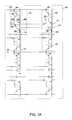
- FIG. 1Ais a schematic diagram depicting an exemplary embodiment of a memory array that includes thyristor-based memory cells.
- FIG. 1Bis a cross-sectional view depicting an exemplary embodiment of a device structure for a thyristor-based memory cell of the memory array of FIG. 1A .
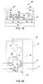
- FIGS. 2A and 2Bare enlarged versions of a portion of the schematic diagram of FIG. 1A depicting an exemplary embodiment of a thyristor-based memory cell, where charge leakage paths are illustratively shown.
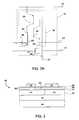
- FIG. 3is a cross-sectional view depicting an exemplary embodiment of a portion of a silicon-on-insulator wafer.
- FIGS. 4A and 4Bare respective cross-sectional views depicting an exemplary embodiment of an in-process thyristor-based memory cell, such as of FIG. 2B , after formation of gate dielectrics.
- FIG. 5Ais the cross-sectional view of FIG. 3 , though after thermal oxidation of exposed surfaces of polysilicon gate electrodes to form a silicon oxide layer.
- FIG. 5Bis the cross-sectional view of FIG. 5A with only an upper portion of the silicon oxide layer removed from an upper surface of the gate electrodes.
- FIG. 5Cis a cross-sectional view depicting the exemplary embodiment as illustratively shown in FIG. 4B , though with rounded corners of the gate electrodes.
- FIG. 5Dis the cross-sectional view of 5 B with a deposited spacer layer in addition to the silicon oxide layer remaining.
- FIG. 5Eis the cross-sectional view of the exemplary embodiment as illustratively shown in FIG. 5C , though having the silicon oxide layer used to form a portion of the offset spacers.
- FIG. 1Ais a schematic diagram depicting an exemplary embodiment of a memory array 100 .
- Memory array 100includes thyristor-based memory cells 101 . Pairs of memory cells 101 may be commonly coupled at a bitline contact 106 for connection to a bitline 110 and may be commonly coupled at a supply voltage contact 107 for connection to a supply voltage line 113 .
- voltage on supply voltage line 113is above both a logic low voltage reference level (“Vss”) and a logic high voltage reference level (“Vdd”), and this supply voltage may be used as an anodic voltage for memory cell 101 .
- Vsslogic low voltage reference level
- Vddlogic high voltage reference level
- VDDAsupply voltage line 113
- supply voltage contact 107is subsequent referred to herein as anode contact 107 .
- Each memory cell 101includes an access device (“transistor”) 108 , which may be a field effect transistor (“FET”), and a thyristor-based storage element 102 .
- access device 108need not be a transistor; however, for purposes of clarity by way of example access device 108 shall be referred to herein as transistor 108 .
- Storage element 102 and transistor 108may be commonly coupled at a node 109 .
- Node 109may be a cathodic node of storage element 102 and a source/drain node of transistor 108 , and thus may be referred to hereafter as cathode node 109 .
- FIG. 1AIllustratively shown in FIG. 1A is an equivalent circuit model of storage element 102 having cross-coupled bi-polar junction transistors (“BJTs”) 103 and 104 , as well as capacitor 105 .
- Storage element 102may be a type of a device known as Thin Capacity Coupled Thyristor (“TCCT”) device. Again, in this example, storage element 102 is coupled in series with an NMOS transistor 108 to provide memory cell 101 . However, a PMOS architecture may be used.
- TCCTThin Capacity Coupled Thyristor
- a gate of access transistor 108is formed from a wordline (“WL 1 ”) 111 in relation to an active area, as generally indicated in FIG. 1A by small dots coupling gates of access transistors 108 to WL 1 s 111 .
- a control gate of storage element 102is formed with another wordline (“WL 2 ”) 112 , as generally indicated by small dots coupling plates of capacitor 105 to WL 2 s 112 .
- WL 1 111 or a WL 2 112may vary from application to application. However, for purposes of clarity by way of example and not limitation, it shall be assumed that there are 144 memory cells coupled to each WL 1 111 and 18 memory cells coupled to each WL 2 112 , though other numbers for either or both may be used.
- An emitter node of BJT 103is coupled to anode voltage line 113 by anode contact 107 .
- a base of BJT 103is coupled to a collector of BJT 104 .
- An emitter of BJT 104is coupled to cathode node 109 .
- a base of BJT 104 and a collector of BJT 103are commonly coupled to a bottom plate of capacitor 105 , and this common coupling location may be generally referred to as storage node 150 .
- FIG. 1Bis a cross-sectional view depicting an exemplary embodiment of a device structure for a memory cell 101 of FIG. 1A .
- memory cell 101is formed using a silicon-on-insulator (“SOI”) wafer having a substrate layer 120 on which a buried oxide (“BOx”) layer 130 is formed. Formed on BOx layer 130 is an active silicon layer 140 . Though a portion of an SOI wafer is generally illustrated in FIG. 1B , other known types of semiconductor wafers may be used.
- SOIsilicon-on-insulator
- anode region 121In active silicon layer 140 , anode region 121 , base region 122 , base region 141 , cathode region 109 , and bitline access region 123 are formed.
- Base region 141is located between base region 122 and cathode region 109 of storage element 102 .
- cathode node 109 and access region 123Between cathode node 109 and access region 123 is access device body region 142 .
- regions 121 , 141 , and 142may be p-type regions, and regions 109 , 122 , and 123 may be n-type regions.
- Above regions 141 and 142may respectively be formed one or more dielectric layers 129 and 124 . Above one or more dielectric layers 124 and 129 may respectively be formed wordlines 111 and 112 of FIG.
- gate electrodes 125 and 126which in association with regions 141 and 142 are defined gate electrodes 125 and 126 , respectively.
- one or more dielectric layers 124 and 129may be the same or different sets of layers.
- one or more dielectric layers (“gate dielectric”) 124 as associated with gate electrode 126may be thinner than one or more dielectric layers (“gate dielectric”) 129 as associated with gate electrode 125 .
- Gate electrode 126is a gate of transistor 108 and an access gate of memory cell 101
- gate electrode 125is a control gate of storage element 102 of memory cell 101 .
- An anode contact 107is coupled to anode region 121
- a bitline contact 106is coupled to access region 123 .
- access region 123 and cathode node 109also serve as source/drain regions of transistor 108 .
- Other details regarding memory cell 101including silicides, extension regions, such as extension region 151 for example, and spacers, among other known details, may be found in U.S. Pat. Nos. 6,767,770 B1 and 6,690,039 B1.
- FIGS. 2A and 2Bare enlarged versions of a portion of the schematic diagram of FIG. 1A depicting an exemplary embodiment of a thyristor-based memory cell 101 , where respective charge leakage paths 201 and 202 are illustratively shown.
- charge leakage paths 201 and 202are further described.
- Charge retention, and thus data retention, of a thyristor-based memory cell 101may be harmed by leakage of such charge stored in memory cell 101 through a gate dielectric, such as leakage through gate dielectric 124 , gate dielectric 129 , or a combination thereof.
- charge stored in storage node 150may leak from base to emitter of BJT 104 , and thus to a source/drain 109 of transistor 108 , and through gate dielectric 124 to gate electrode 126 of transistor 108 , as generally indicated by charge leakage path 201 .
- Such charge leakage, having arrived at WL 1 111is leaked out onto such wordline, thereby reducing stability of memory cell 101 .
- Another possible charge leakage pathis from storage node 150 through gate dielectric 129 to WL 2 112 , which is used to provide gate electrode 125 or an upper plate of capacitor 105 . On reaching gate electrode 125 , such charge may leak out onto WL 2 112 , as generally indicated by charge leakage path page 202 , as illustratively shown in FIG. 2B .
- charge in base region 141may leak to cathode node 109 and into extension region 151 and then to and through gate dielectric 124 to gate electrode 126 .
- Charge leakage path 202is from base region 141 to and through gate dielectric 129 to gate electrode 125 .
- base region 141may be thought of as providing storage node 150 of memory cell 101 .
- Time-averaged standby currentis approximately memory cell 101 read current, as limited by transistor 109 (“FET”), times the duty cycle during which the FET is on.
- Standby power associated with restoring memory cell 101is proportional to frequency with which memory cell is restored.
- Such restore frequency of memory cell 101depends at least in part on storage capacitance and bipolar gain of memory cell 101 .
- dynamic standby current for memory cell 101depends at least in part on storage capacitance and internal amplification of such memory cell 101 .
- Charge leakage path 201removes charge from storage capacitance through gate dielectric 124 . This charge leakage through gate dielectric 124 impacts the time interval which memory cell 101 can tolerate between restore operations and still be sufficiently stable to yield a proper data state when read. Reducing charge leakage via charge leakage path 201 facilitates less frequent restore operations while maintaining proper data state of memory cell 101 when read. A reduction in the frequency of such restore operations may result in a reduction in standby power consumption in accordance with the above-described relationship to dynamic standby current and storage capacitance.
- charge leakage path 201is equally applicable to charge leakage path 202 .
- reducing the amount of charge leakage via either or both of charge leakage paths 201 and 202facilitates a longer time interval between restore pulsing of memory cell 101 , as well as a reduction in standby power consumption.
- solution spacesthere are three “solution spaces,” described below, for increasing charge retention of memory cell 101 by reducing leakage current via reducing charge leakage.
- solution spacesit is meant to generally indicate an approach to reducing charge leakage in a thyristor-based memory cell, and it is not meant to include any particular details as they may be varied as described below.
- One of these solution spacesmay be used, or a combination of any two of these solutions spaces may be used, or a combination of all three of these solution spaces may be used.
- One solution spaceis to make a gate dielectric less susceptible to charge tunneling by using a higher permittivity material to reduce charge leakage through either or both of charge leakage paths 201 and 202 .
- higher permittivity materialit is generally meant that dielectric constant, k, of the material is greater than 4.0.
- a second solution spaceis to reduce the effective area of a gate dielectric in which tunneling currents occur.
- a third solution spaceis to use a locally increased thickness in a region where tunneling current occurs across a gate dielectric. This local increase in thickness may be achieved using a “polysilicon reoxidation,” as described below in additional detail. Again, it should be understood that any one, any combination of two, or all three of these solution spaces may be applied.
- FIG. 3is a cross-sectional view depicting an exemplary embodiment of a portion of an SOI wafer 152 .
- Formed in silicon layer 140are regions 141 and 142 . Regions 141 and 142 may be formed in a known manner.
- An interfacial layer 301is deposited on an exposed surface of silicon layer 140 .
- Dielectric layer 302is deposited immediately above an exposed upper surface of interfacial layer 301 .
- Dielectric layer 302is a “high k” dielectric layer having a dielectric constant greater than 4.0.
- Another interfacial layer 303is deposited immediately above an exposed upper surface of dielectric layer 302 .
- layers 301 through 303 in combinationhave a thickness 300 .
- layers 301 , 302 , and 303are actually much thinner than illustratively shown, and have been enlarged for reasons of visibility to the detriment of perspective.
- Thickness 310 of dielectric layer 302due to the high permittivity of such dielectric layer, may provide blocking of tunneling current. Electrons, and holes, quantum mechanically tunnel through layers, such as layers 301 through 303 . Capacitance, which is conventionally surface area times the permittivity divided by the dielectric thickness, is a well known equation, and thus is not described herein in detail. Notably, for operation of a thyristor-based memory cell 101 , such as of FIG. 1B , the relative surface area of capacitors formed at least in part with respect to gate electrodes 125 and 126 may be decreased, along with gate dielectric thickness, while increasing permittivity of the gate dielectric in order to obtain a target capacitance.
- a thyristor-based memory cellmay be in a range of approximately 0.05 to 0.50 femtofarads, where thickness 310 in this embodiment is in a range of approximately 4 nm to 8 nm.
- interfacial layers 301 and 303may be determined at least in part by the reactivity of dielectric layer 302 to either or both silicon layer 140 and gate electrode material, such as that used to form either or both gate electrodes 125 and 126 .
- interfacial layers 301 or 303may be omitted depending on degree of tolerance of reactivity of dielectric layer 302 to other materials used.
- materials that may be used for dielectric layer 302include a silicon oxynitride, silicon nitride, or an aluminum oxide (e.g., Al 2 O 3 ). These examples of oxides have a dielectric constant k generally in a range of 4 to 10.
- gate dielectricssuch as unary oxides or silicates, having a dielectric constant in a range of approximately 10 to 20 may be used.
- unary oxidesinclude zirconium oxide (e.g., ZrO 2 ), hafnium oxide (e.g., HfO 2 ), yttrium oxide (e.g., Y 2 O 3 ), lanthanum oxide (e.g., La 2 O 3 ), gadolinium oxide (e.g., Gd 2 O 3 ), and scandium oxide (e.g., Sc 2 O 3 ).
- silicatesexamples include any of zirconium, hafnium, lanthanum, or yttrium oxides reacted with a silicon dioxide (e.g., ((Zr, Hf, La, Y)O 2 ) y .(SiO 2 ) 1-y ).
- a hafnium silicatee.g., HfSi x O y
- a nitrided silicatemay be used, such as a nitrided hafnium silicate (e.g., HfSi x O y N z ) for example.
- Higher k dielectricssuch as amorphous and single crystal materials, having a dielectric constant greater than approximately 20 may be used for a gate dielectric.
- amorphous materialsinclude lanthanum and yttrium aluminates, as well as rare earth aluminate alloys.
- single crystal materialsthat may be used include lanthanum aluminum oxide (e.g., LaAl 3 O 4 ), barium zirconium oxide (e.g., BaZrO 3 ), yttrium oxide, and lanthanum oxide, as previously mentioned with respect to unary oxides.
- Examples of materials that may be used for either or both of interfacial layers 301 and 303include nitrogen-doped silicon oxide, silicon oxynitride, and aluminum oxide (e.g., Al 2 O 3 ). Nitrogen-doped silicon oxide may have a less nitrogen content than silicon oxynitride. Silicon oxynitride may encompass known SiO x N y stoichiometry values.
- Known methods of deposition for forming layers 301 , 302 , and 303include furnace deposition, rapid plasma enhanced chemical vapor deposition (RPECVD), rapid thermal chemical vapor deposition (RTCVD), jet vapor deposition (JVD), molecular beam epitaxy (MBE), metal organic chemical vapor deposition (MOCVD), atomic layer chemical vapor deposition (ALCVD), and oxidation of metals, among other known types of deposition.
- RPECVDrapid plasma enhanced chemical vapor deposition
- RTCVDrapid thermal chemical vapor deposition
- JVDjet vapor deposition
- MBEmolecular beam epitaxy
- MOCVDmetal organic chemical vapor deposition
- ACVDatomic layer chemical vapor deposition
- oxidation of metalsamong other known types of deposition.
- materials having a dielectric constant greater than 4that may be used for forming dielectric layer 302 other than hafnium oxide including hafnium silicate (e.g., HfSi x O y ) and nitrided hafnium silicate (e.g., HfSi x O y N z ).
- hafnium silicatee.g., HfSi x O y
- nitrided hafnium silicatee.g., HfSi x O y N z
- Known types of deposition of a hafnium oxide, a hafnium silicate, a nitrided hafnium silicate, or a silicon oxynitridemay include a form of chemical vapor deposition (CVD), including atomic layer deposition (ALD or ALCVD).
- CVDchemical vapor deposition
- ALCVDatomic layer deposition
- Gate electrodes 125 and 126may be formed of the same or different materials. With respect to using the same materials, such electrodes 125 and 126 may be formed of silicided polysilicon, such as cobalt silicide (e.g., CoSi 2 ), nickel silicide (e.g., NiSi), or silicon germanium (e.g., SiGe). Notably, other known germanides may be used. Alternatively, different materials may be used to form gate electrodes 125 and 126 .
- material used to form gate electrode 126may include tantalum, tantalum nitride (e.g., TaN), zirconium, hafnium, or a metal silicide (e.g., MSi x ; where the metal is zirconium or hafnium), a metal nitride (e.g., MN x ; where the metal is zirconium or hafnium), or a metal silicon nitride (e.g., MSi x N y ; where the metal is zirconium or hafnium).
- Examples of materials that may be used for providing gate electrode 125 for storage element 102include platinum, ruthenium, ruthenium iridium oxide (e.g., RuO 2 Ir), nickel, cobalt, tungsten nitride (e.g., WN), or a metal silicide, metal nitride, or a metal silicon nitride, as previously mentioned with respect to gate electrode 126 .
- Known types of deposition for forming either or both of gate electrodes 126 or 125include various forms of CVD, as previously mentioned, and sputter deposition, among other known types of deposition.
- gate dielectric deposition and gate electrode deposition toolsmay be clustered.
- FIGS. 4A and 4Bare respective cross-sectional views depicting an exemplary embodiment of an in-process thyristor-based memory cell 101 , such as of FIG. 2B , after formation of gate dielectrics.
- gate dielectricsmay be formed of one or more of layers 301 , 302 , and 303 .
- FIGS. 4A and 4Ban implementation of the second solution space is considered.
- SOI wafer 152has already had formation of isolation regions, implantation of wells, formation of gate dielectrics, formation of gate electrodes 125 and 126 , and associated gate dielectric and gate electrode patterning.
- Gate dielectric layers 301 , 302 , and 303may be etched at least in part during the etching to form gate electrodes 125 and 126 .
- spacer materialhas been deposited, and an isotropic etch has been performed in order to form spacers 401 .
- spacer materialare well known and include forms of silicon oxides.
- these “zero spacers” or offset spacers 401are formed by deposition of one or more layers.
- spacers 401extend to an upper surface of silicon layer 140 , and generally dielectric layers, such as one or more of layers 301 , 302 , and 303 , do not generally extend under spacers 401 .
- Implant 403is provided to SOI wafer 152 after formation and patterning of a mask 402 , such as from a resist, to protect storage element 102 of FIG. 1A .
- Implant 403is a shallow implant used to form extension regions.
- implant 403may be an n-type dopant, such as arsenic, implanted at an angle of approximately 0 to 7 degrees from vertical to an upper surface of SOI wafer 152 at a conventional implant energy and dosage.
- shallow implant 403may implant into exposed gate electrode 126 , for example, implant 403 is to form shallow implant regions 404 in exposed silicon layer 140 .
- Shallow implant regions 404are used to provide extension regions, such as extension regions 451 at least in part responsive to sidewalls 405 of offset spacers 401 . Notably, because spacers 401 are in place prior to and during implant 403 , extension regions 451 are effectively disposed away from sidewalls of gate electrode 126 . In other words, extension regions 451 formed by shallow implant regions 404 are formed in part responsive to exposed sidewalls of spacers 401 .
- extension regionsAs is known with respect to extension regions, the further an extension region is away from an edge of a gate electrode, the greater the source/drain resistance, sometimes referred to as the “series resistance,” of the transistor, such as the transistor formed in part using gate electrode 126 .
- series resistancesometimes referred to as the “series resistance” of the transistor, such as the transistor formed in part using gate electrode 126 .
- An increase of series resistancemeans that additional drive current may be needed to operate such a transistor.
- extension regionsconventionally are not far removed from an edge of a gate electrode in order to reach a target drive current.
- gate-to-drain capacitancesometimes referred to as “overlap capacitance,” generally caused by an extension region extending under a gate electrode, increases the further such extension region extends under such gate electrode.
- overlap capacitancecan slow operation of a transistor.
- series resistancemay be increased to increase charge retention time.
- the extension region associated with the right side of gate electrode 126is effectively pulled away from such gate electrode responsive to the presence of an offset spacer 401 on that side.
- Offset spacer 401is greater in horizontal thickness than a conventional zero spacer, in that it is at least 10 nanometers (“nm”) wide.
- gate overlap between gate electrode 126 and extension region 451there is less gate overlap between gate electrode 126 and extension region 451 . More particularly, subsequent thermal cycling of SOI wafer 152 due to subsequent processing may cause shallow implant region 404 to laterally defuse. By having offset spacer 401 , the overlap between extension region 451 and gate electrode 126 is reduced. By reducing the overlap, the leakage current via charge leakage path 201 is reduced, again charge leakage via path charge leakage path 201 is made less preferential. Accordingly, data retention time of a thyristor-based memory cell 101 may be increased.
- a spacer materialsuch as a dielectric, including a silicon oxide, silicon nitride, or a combination thereof
- an isotropic etchis done to form spacers 414 along sidewalls of offset spacers 401 .
- a thin oxide layermay be formed, such as by deposition, along an exposed upper surface of silicon layer 140 prior to forming spacers 414 but after the formation of shallow implant regions (“shallow extension regions”) 404 .
- implants forming regions 122 and 121 of FIG. 1Bmay be done.
- dielectric layer 413may be conformally deposited, masked with a pattern mask, and etched to form dielectric layer 413 .
- Dielectric layer 413may be used to cover a portion of gate electrode 125 and regions 122 to block slicidation of such portion of gate electrode 125 and regions 122 during subsequent processing.
- a resistmay be deposited and patterned to form resist layer 412 to protect regions 121 of FIG. 1B from implant 430 .
- implant 430may implant into other areas, such as gate electrode 126 and a portion of gate electrode 125 , implant 430 is to form source/drain type regions for cathode region 109 and access region 123 .
- thesemay be n+ regions formed using an n-type dopant, such as arsenic or phosphorus, implanted at an angle of approximately 0 to 7 degrees from vertical to a surface of silicon layer 140 .
- Regions 109 and 123may extend to BOx layer 130 .
- implant 430is responsive to spacers 414 with respect to implantation into silicon layer 140 , though some lateral implantation or diffusion may result such that regions 109 and 123 partially extend under one or more spacers 414 .
- implant regions 109 and 123are pulled back further away from gate electrode 126 and an unmasked portion of gate electrode 125 .
- shallow implant region 404as an extension of cathode region 109 , namely where the combination is effectively a cathode node 109 , there is less opportunity for charge leakage from cathode node 109 to tunnel through gate dielectric 302 as associated with gate electrode 126 .
- the probability of leakage current via charge leakage path 201is reduced. Accordingly, data retention time of a thyristor-based memory cell 101 may be increased.
- FIG. 5Ais a cross-sectional view of FIG. 3 though after thermal oxidation of exposed surfaces of polysilicon gate electrodes 125 and 126 to form a silicon oxide layer 501 .
- thermal oxidation of polysilicon gate electrodes 125 and 126causes rounding, and thus undercutting of corners of such gate electrodes.
- FIG. 5Bwhere there is shown the cross-sectional view of FIG. 5A after removal of an upper portion of silicon oxide layer 501 .
- regions 502are undercut regions. Undercut regions 502 undercut gate electrode 126 in proximity to the location of extension regions 451 of FIG. 4B .
- FIG. 5Cis a cross-sectional view depicting the exemplary embodiment as illustratively shown in FIG. 4B , though with rounded corners of gate electrodes 125 and 126 .
- FIG. 5Cis a cross-sectional view depicting the exemplary embodiment as illustratively shown in FIG. 4B , though with rounded corners of gate electrodes 125 and 126 .
- offset spacers 401laterally extends under gate electrodes 125 and 126 . This lateral extension or “bird's beak” creates a greater dielectric separation between gate electrodes 125 and 126 with respect to active silicon of silicon layer 140 and a bottom surface of such gate electrodes.
- charge stored in base region 141has a larger dielectric boundary from what was the preferential leakage path owing to providing an undercut region 502 of FIG. 5B .
- charge leakagemay be reduced, and thus thyristor-based memory cell 101 may have a longer data retention time.
- an upper portion of silicon oxide layer 501may be removed from an upper surface of gate electrodes 125 and 126 while leaving silicon oxide layer 501 at least under corners of gate electrodes 125 and 126 .
- Such removalmay be accomplished by a blanket etchback.
- a blanket etchback(not shown) may be an anisotropic etch approximately perpendicular to the surface of silicon layer 140 .
- silicon oxide layer 501may be substantially left in place along sidewalls of gate electrodes 125 and 126 and under corners thereof.
- oxidation of polysilicon electrodes 125 and 126may be done after patterning associated gate dielectrics.
- Thickness of silicon oxide layer 501may be approximately 100 or more nm thick and, more particularly, may be approximately 150 nm thick. Accordingly, to build up an offset spacer, a spacer material may be deposited and etched with a spacer etch to form offset spacer 510 next to silicon oxide layers 510 along sidewalls of gate electrodes 125 and 126 . Thus, a thicker offset may be controllably formed prior to formation of offset spacer 401 .
- local silicon oxide thickeningmay be done using a precursor implant into the area targeted for thickening.
- an angled implant under corners of gate electrode 126may be done to accelerate oxidation of a portion of active silicon layer 140 to cause locally thicker silicon oxide under such corners.
- FIG. 5Eis the cross-sectional view of the exemplary embodiment as illustratively shown in FIG. 5C , though having offset spacer 510 and silicon oxide layer 501 used to form a portion of offset spacing in addition to offset spacer 401 .
- offset spacer 510 and silicon oxide layer 501are illustratively shown where both materials have merged.
- the material used to form offset spacer 510need not be the same type of material as silicon oxide layer 501 .
- the material used to form offset spacer 510may be the same or different from the material used to form offset spacer 401 . Materials previously described herein may be used for formation of spacer 510 .
- gate electrodes 125 and 126have rounded corners.
- silicon oxide layer 501 along at least the right sidewall of gate electrode 126 in FIG. 5Dtogether with offset spacers 510 and 401 along such right-side silicon oxide layer 501 of FIG. 5D , provide an offset for formation of extension region 451 , at least along such right side in FIG. 5E , spaced away from a right side sidewall of gate electrode 126 .
- silicon oxide layer 501 of FIG. 5Dprovides a dielectric barrier to tunneling current under at least a right side corner of gate electrode 126 , charge leakage from extension region 451 to gate electrode 126 is inhibited.
Landscapes
- Semiconductor Memories (AREA)
Abstract
Description
Claims (10)
Priority Applications (1)
| Application Number | Priority Date | Filing Date | Title |
|---|---|---|---|
| US11/303,237US7786505B1 (en) | 2005-12-16 | 2005-12-16 | Reduction of charge leakage from a thyristor-based memory cell |
Applications Claiming Priority (1)
| Application Number | Priority Date | Filing Date | Title |
|---|---|---|---|
| US11/303,237US7786505B1 (en) | 2005-12-16 | 2005-12-16 | Reduction of charge leakage from a thyristor-based memory cell |
Publications (1)
| Publication Number | Publication Date |
|---|---|
| US7786505B1true US7786505B1 (en) | 2010-08-31 |
Family
ID=42646638
Family Applications (1)
| Application Number | Title | Priority Date | Filing Date |
|---|---|---|---|
| US11/303,237Expired - Fee RelatedUS7786505B1 (en) | 2005-12-16 | 2005-12-16 | Reduction of charge leakage from a thyristor-based memory cell |
Country Status (1)
| Country | Link |
|---|---|
| US (1) | US7786505B1 (en) |
Cited By (22)
| Publication number | Priority date | Publication date | Assignee | Title |
|---|---|---|---|---|
| US6123962A (en)* | 1986-02-13 | 2000-09-26 | Takeda Chemical Industries, Inc. | Process for producing stabilized pharmaceutical composition |
| US20110215436A1 (en)* | 2010-03-02 | 2011-09-08 | Micron Technology, Inc. | Semiconductor devices including a diode structure over a conductive strap and methods of forming such semiconductor devices |
| US20110215426A1 (en)* | 2010-03-04 | 2011-09-08 | Kabushiki Kaisha Toshiba | Semiconductor device and manufacturing method of semiconductor device |
| US8519431B2 (en) | 2011-03-08 | 2013-08-27 | Micron Technology, Inc. | Thyristors |
| US8809145B2 (en) | 2010-03-02 | 2014-08-19 | Micron Technology, Inc. | Semiconductor cells, arrays, devices and systems having a buried conductive line and methods for forming the same |
| US8841715B2 (en) | 2010-03-02 | 2014-09-23 | Micron Technology, Inc. | Floating body cell structures, devices including same, and methods for forming same |
| US8980699B2 (en) | 2010-03-02 | 2015-03-17 | Micron Technology, Inc. | Thyristor-based memory cells, devices and systems including the same and methods for forming the same |
| US9129983B2 (en) | 2011-02-11 | 2015-09-08 | Micron Technology, Inc. | Memory cells, memory arrays, methods of forming memory cells, and methods of forming a shared doped semiconductor region of a vertically oriented thyristor and a vertically oriented access transistor |
| US9209187B1 (en) | 2014-08-18 | 2015-12-08 | Micron Technology, Inc. | Methods of forming an array of gated devices |
| US9224738B1 (en) | 2014-08-18 | 2015-12-29 | Micron Technology, Inc. | Methods of forming an array of gated devices |
| US9269795B2 (en) | 2011-07-26 | 2016-02-23 | Micron Technology, Inc. | Circuit structures, memory circuitry, and methods |
| WO2016049590A1 (en)* | 2014-09-25 | 2016-03-31 | Kilopass Technology, Inc. | Cross-coupled thyristor sram semiconductor structures and methods of fabrication |
| WO2016049599A1 (en)* | 2014-09-25 | 2016-03-31 | Kilopass Technology, Inc. | Write assist sram circuits and methods of operation |
| WO2016049594A1 (en)* | 2014-09-25 | 2016-03-31 | Kilopass Technology, Inc. | Two-transistor sram semiconductor structure and methods of fabrication |
| US9564199B2 (en) | 2014-09-25 | 2017-02-07 | Kilopass Technology, Inc. | Methods of reading and writing data in a thyristor random access memory |
| US9564441B2 (en) | 2014-09-25 | 2017-02-07 | Kilopass Technology, Inc. | Two-transistor SRAM semiconductor structure and methods of fabrication |
| US9608119B2 (en) | 2010-03-02 | 2017-03-28 | Micron Technology, Inc. | Semiconductor-metal-on-insulator structures, methods of forming such structures, and semiconductor devices including such structures |
| US9673054B2 (en) | 2014-08-18 | 2017-06-06 | Micron Technology, Inc. | Array of gated devices and methods of forming an array of gated devices |
| US9741413B2 (en) | 2014-09-25 | 2017-08-22 | Kilopass Technology, Inc. | Methods of reading six-transistor cross-coupled thyristor-based SRAM memory cells |
| US9837418B2 (en) | 2014-09-25 | 2017-12-05 | Kilopass Technology, Inc. | Thyristor volatile random access memory and methods of manufacture |
| US10090037B2 (en) | 2014-09-25 | 2018-10-02 | Tc Lab, Inc. | Methods of retaining and refreshing data in a thyristor random access memory |
| US10373956B2 (en) | 2011-03-01 | 2019-08-06 | Micron Technology, Inc. | Gated bipolar junction transistors, memory arrays, and methods of forming gated bipolar junction transistors |
Citations (44)
| Publication number | Priority date | Publication date | Assignee | Title |
|---|---|---|---|---|
| US20020004263A1 (en)* | 1998-05-20 | 2002-01-10 | Yoshikazu Tanabe | Process for producing semiconductor integrated circuit device and semiconductor integrated circuit device |
| US6462359B1 (en)* | 2001-03-22 | 2002-10-08 | T-Ram, Inc. | Stability in thyristor-based memory device |
| US6583452B1 (en) | 2001-12-17 | 2003-06-24 | T-Ram, Inc. | Thyristor-based device having extended capacitive coupling |
| US6611452B1 (en) | 2002-04-05 | 2003-08-26 | T-Ram, Inc. | Reference cells for TCCT based memory cells |
| US6653174B1 (en) | 1998-06-05 | 2003-11-25 | T-Ram, Inc. | Thyristor-based device over substrate surface |
| US6666481B1 (en) | 2002-10-01 | 2003-12-23 | T-Ram, Inc. | Shunt connection to emitter |
| US6683330B1 (en) | 2002-10-01 | 2004-01-27 | T-Ram, Inc. | Recessed thyristor control port |
| US6686612B1 (en) | 2002-10-01 | 2004-02-03 | T-Ram, Inc. | Thyristor-based device adapted to inhibit parasitic current |
| US6690039B1 (en) | 2002-10-01 | 2004-02-10 | T-Ram, Inc. | Thyristor-based device that inhibits undesirable conductive channel formation |
| US6690038B1 (en) | 1999-06-05 | 2004-02-10 | T-Ram, Inc. | Thyristor-based device over substrate surface |
| US6703646B1 (en) | 2002-09-24 | 2004-03-09 | T-Ram, Inc. | Thyristor with lightly-doped emitter |
| US6721220B2 (en) | 2002-07-05 | 2004-04-13 | T-Ram, Inc. | Bit line control and sense amplification for TCCT-based memory cells |
| US6727528B1 (en) | 2001-03-22 | 2004-04-27 | T-Ram, Inc. | Thyristor-based device including trench dielectric isolation for thyristor-body regions |
| US6734815B1 (en) | 2003-03-25 | 2004-05-11 | T-Ram, Inc. | Geometric D/A converter for a delay-locked loop |
| US6735113B2 (en) | 2002-10-15 | 2004-05-11 | T-Ram, Inc. | Circuit and method for implementing a write operation with TCCT-based memory cells |
| US6756838B1 (en) | 2003-03-18 | 2004-06-29 | T-Ram, Inc. | Charge pump based voltage regulator with smart power regulation |
| US6756612B1 (en) | 2002-10-28 | 2004-06-29 | T-Ram, Inc. | Carrier coupler for thyristor-based semiconductor device |
| US6767770B1 (en)* | 2002-10-01 | 2004-07-27 | T-Ram, Inc. | Method of forming self-aligned thin capacitively-coupled thyristor structure |
| US6778435B1 (en) | 2002-06-12 | 2004-08-17 | T-Ram, Inc. | Memory architecture for TCCT-based memory cells |
| US6781888B1 (en) | 2002-03-18 | 2004-08-24 | T-Ram, Inc. | Reference cells for TCCT based memory cells |
| US6785169B1 (en) | 2002-04-05 | 2004-08-31 | T-Ram, Inc. | Memory cell error recovery |
| US6790713B1 (en) | 2002-09-09 | 2004-09-14 | T-Ram, Inc. | Method for making an inlayed thyristor-based device |
| US6804162B1 (en) | 2001-04-05 | 2004-10-12 | T-Ram, Inc. | Read-modify-write memory using read-or-write banks |
| US6815734B1 (en) | 2002-10-01 | 2004-11-09 | T-Ram, Inc. | Varied trench depth for thyristor isolation |
| US6818482B1 (en) | 2002-10-01 | 2004-11-16 | T-Ram, Inc. | Method for trench isolation for thyristor-based device |
| US6828202B1 (en) | 2002-10-01 | 2004-12-07 | T-Ram, Inc. | Semiconductor region self-aligned with ion implant shadowing |
| US6885581B2 (en) | 2001-04-05 | 2005-04-26 | T-Ram, Inc. | Dynamic data restore in thyristor-based memory device |
| US6888177B1 (en) | 2002-09-24 | 2005-05-03 | T-Ram, Inc. | Increased base-emitter capacitance |
| US6888176B1 (en)* | 2002-10-01 | 2005-05-03 | T-Ram, Inc. | Thyrister semiconductor device |
| US6891205B1 (en) | 2001-03-22 | 2005-05-10 | T-Ram, Inc. | Stability in thyristor-based memory device |
| US6891774B1 (en) | 2003-09-03 | 2005-05-10 | T-Ram, Inc. | Delay line and output clock generator using same |
| US6903987B2 (en) | 2002-08-01 | 2005-06-07 | T-Ram, Inc. | Single data line sensing scheme for TCCT-based memory cells |
| US6913955B1 (en) | 2002-10-01 | 2005-07-05 | T-Ram, Inc. | Method of manufacturing a thyristor device with a control port in a trench |
| US6937085B1 (en) | 2003-04-25 | 2005-08-30 | T-Ram, Inc. | Sense amplifier based voltage comparator |
| US6944051B1 (en) | 2003-10-29 | 2005-09-13 | T-Ram, Inc. | Data restore in thryistor based memory devices |
| US6947349B1 (en) | 2003-09-03 | 2005-09-20 | T-Ram, Inc. | Apparatus and method for producing an output clock pulse and output clock generator using same |
| US6953953B1 (en) | 2002-10-01 | 2005-10-11 | T-Ram, Inc. | Deep trench isolation for thyristor-based semiconductor device |
| US6955965B1 (en)* | 2003-12-09 | 2005-10-18 | Fasl, Llc | Process for fabrication of nitride layer with reduced hydrogen content in ONO structure in semiconductor device |
| US6965129B1 (en) | 2002-11-06 | 2005-11-15 | T-Ram, Inc. | Thyristor-based device having dual control ports |
| US6975260B1 (en) | 2003-03-25 | 2005-12-13 | T-Ram, Inc. | Geometric D/A converter for a delay-locked loop |
| US6980457B1 (en) | 2002-11-06 | 2005-12-27 | T-Ram, Inc. | Thyristor-based device having a reduced-resistance contact to a buried emitter region |
| US6998298B1 (en) | 2003-08-11 | 2006-02-14 | T-Ram Semiconductor, Inc. | Thyristor semiconductor memory device and method of manufacture |
| US6998652B1 (en) | 2002-10-01 | 2006-02-14 | T-Ram, Inc. | Trench isolation for thyristor-based device |
| US7381999B1 (en)* | 2005-07-21 | 2008-06-03 | T-Ram Semiconductor, Inc. | Workfunction-adjusted thyristor-based memory device |
- 2005
- 2005-12-16USUS11/303,237patent/US7786505B1/ennot_activeExpired - Fee Related
Patent Citations (57)
| Publication number | Priority date | Publication date | Assignee | Title |
|---|---|---|---|---|
| US20020004263A1 (en)* | 1998-05-20 | 2002-01-10 | Yoshikazu Tanabe | Process for producing semiconductor integrated circuit device and semiconductor integrated circuit device |
| US6653174B1 (en) | 1998-06-05 | 2003-11-25 | T-Ram, Inc. | Thyristor-based device over substrate surface |
| US6690038B1 (en) | 1999-06-05 | 2004-02-10 | T-Ram, Inc. | Thyristor-based device over substrate surface |
| US6727528B1 (en) | 2001-03-22 | 2004-04-27 | T-Ram, Inc. | Thyristor-based device including trench dielectric isolation for thyristor-body regions |
| US6462359B1 (en)* | 2001-03-22 | 2002-10-08 | T-Ram, Inc. | Stability in thyristor-based memory device |
| US6653175B1 (en) | 2001-03-22 | 2003-11-25 | T-Ram, Inc. | Stability in thyristor-based memory device |
| US6835997B1 (en) | 2001-03-22 | 2004-12-28 | T-Ram, Inc. | Thyristor-based device with trench dielectric material |
| US6891205B1 (en) | 2001-03-22 | 2005-05-10 | T-Ram, Inc. | Stability in thyristor-based memory device |
| US6777271B1 (en) | 2001-03-22 | 2004-08-17 | T-Ram, Inc. | Thyristor-based device including trench isolation |
| US6885581B2 (en) | 2001-04-05 | 2005-04-26 | T-Ram, Inc. | Dynamic data restore in thyristor-based memory device |
| US6804162B1 (en) | 2001-04-05 | 2004-10-12 | T-Ram, Inc. | Read-modify-write memory using read-or-write banks |
| US6583452B1 (en) | 2001-12-17 | 2003-06-24 | T-Ram, Inc. | Thyristor-based device having extended capacitive coupling |
| US6940772B1 (en) | 2002-03-18 | 2005-09-06 | T-Ram, Inc | Reference cells for TCCT based memory cells |
| US6781888B1 (en) | 2002-03-18 | 2004-08-24 | T-Ram, Inc. | Reference cells for TCCT based memory cells |
| US6901021B1 (en) | 2002-03-18 | 2005-05-31 | T-Ram, Inc. | Reference cells for TCCT based memory cells |
| US6785169B1 (en) | 2002-04-05 | 2004-08-31 | T-Ram, Inc. | Memory cell error recovery |
| US6845037B1 (en) | 2002-04-05 | 2005-01-18 | T-Ram, Inc. | Reference cells for TCCT based memory cells |
| US6611452B1 (en) | 2002-04-05 | 2003-08-26 | T-Ram, Inc. | Reference cells for TCCT based memory cells |
| US6778435B1 (en) | 2002-06-12 | 2004-08-17 | T-Ram, Inc. | Memory architecture for TCCT-based memory cells |
| US6721220B2 (en) | 2002-07-05 | 2004-04-13 | T-Ram, Inc. | Bit line control and sense amplification for TCCT-based memory cells |
| US6958931B1 (en) | 2002-07-05 | 2005-10-25 | T-Ram, Inc. | Bit line control and sense amplification for TCCT-based memory cells |
| US6903987B2 (en) | 2002-08-01 | 2005-06-07 | T-Ram, Inc. | Single data line sensing scheme for TCCT-based memory cells |
| US7006398B1 (en) | 2002-08-01 | 2006-02-28 | T-Ram, Inc. | Single data line sensing scheme for TCCT-based memory cells |
| US6790713B1 (en) | 2002-09-09 | 2004-09-14 | T-Ram, Inc. | Method for making an inlayed thyristor-based device |
| US6888177B1 (en) | 2002-09-24 | 2005-05-03 | T-Ram, Inc. | Increased base-emitter capacitance |
| US6828176B1 (en) | 2002-09-24 | 2004-12-07 | T-Ram, Inc. | Thyristor having a first emitter with relatively lightly doped portion to the base |
| US6703646B1 (en) | 2002-09-24 | 2004-03-09 | T-Ram, Inc. | Thyristor with lightly-doped emitter |
| US6913955B1 (en) | 2002-10-01 | 2005-07-05 | T-Ram, Inc. | Method of manufacturing a thyristor device with a control port in a trench |
| US6911680B1 (en) | 2002-10-01 | 2005-06-28 | T-Ram, Inc. | Self-aligned thin capacitively-coupled thyristor structure |
| US6828202B1 (en) | 2002-10-01 | 2004-12-07 | T-Ram, Inc. | Semiconductor region self-aligned with ion implant shadowing |
| US6666481B1 (en) | 2002-10-01 | 2003-12-23 | T-Ram, Inc. | Shunt connection to emitter |
| US6815734B1 (en) | 2002-10-01 | 2004-11-09 | T-Ram, Inc. | Varied trench depth for thyristor isolation |
| US6686612B1 (en) | 2002-10-01 | 2004-02-03 | T-Ram, Inc. | Thyristor-based device adapted to inhibit parasitic current |
| US6767770B1 (en)* | 2002-10-01 | 2004-07-27 | T-Ram, Inc. | Method of forming self-aligned thin capacitively-coupled thyristor structure |
| US6683330B1 (en) | 2002-10-01 | 2004-01-27 | T-Ram, Inc. | Recessed thyristor control port |
| US6888176B1 (en)* | 2002-10-01 | 2005-05-03 | T-Ram, Inc. | Thyrister semiconductor device |
| US6998652B1 (en) | 2002-10-01 | 2006-02-14 | T-Ram, Inc. | Trench isolation for thyristor-based device |
| US6979602B1 (en) | 2002-10-01 | 2005-12-27 | T-Ram, Inc. | Method for making a recessed thyristor control port |
| US6690039B1 (en) | 2002-10-01 | 2004-02-10 | T-Ram, Inc. | Thyristor-based device that inhibits undesirable conductive channel formation |
| US6818482B1 (en) | 2002-10-01 | 2004-11-16 | T-Ram, Inc. | Method for trench isolation for thyristor-based device |
| US6953953B1 (en) | 2002-10-01 | 2005-10-11 | T-Ram, Inc. | Deep trench isolation for thyristor-based semiconductor device |
| US6735113B2 (en) | 2002-10-15 | 2004-05-11 | T-Ram, Inc. | Circuit and method for implementing a write operation with TCCT-based memory cells |
| US6756612B1 (en) | 2002-10-28 | 2004-06-29 | T-Ram, Inc. | Carrier coupler for thyristor-based semiconductor device |
| US6872602B1 (en) | 2002-10-28 | 2005-03-29 | T-Ram, Inc. | Carrier coupler for thyristor-based semiconductor device |
| US6965129B1 (en) | 2002-11-06 | 2005-11-15 | T-Ram, Inc. | Thyristor-based device having dual control ports |
| US6980457B1 (en) | 2002-11-06 | 2005-12-27 | T-Ram, Inc. | Thyristor-based device having a reduced-resistance contact to a buried emitter region |
| US6756838B1 (en) | 2003-03-18 | 2004-06-29 | T-Ram, Inc. | Charge pump based voltage regulator with smart power regulation |
| US6734815B1 (en) | 2003-03-25 | 2004-05-11 | T-Ram, Inc. | Geometric D/A converter for a delay-locked loop |
| US6975260B1 (en) | 2003-03-25 | 2005-12-13 | T-Ram, Inc. | Geometric D/A converter for a delay-locked loop |
| US6819278B1 (en) | 2003-03-25 | 2004-11-16 | T-Ram, Inc. | Geometric D/A converter for a delay-locked loop |
| US6937085B1 (en) | 2003-04-25 | 2005-08-30 | T-Ram, Inc. | Sense amplifier based voltage comparator |
| US6998298B1 (en) | 2003-08-11 | 2006-02-14 | T-Ram Semiconductor, Inc. | Thyristor semiconductor memory device and method of manufacture |
| US6947349B1 (en) | 2003-09-03 | 2005-09-20 | T-Ram, Inc. | Apparatus and method for producing an output clock pulse and output clock generator using same |
| US6891774B1 (en) | 2003-09-03 | 2005-05-10 | T-Ram, Inc. | Delay line and output clock generator using same |
| US6944051B1 (en) | 2003-10-29 | 2005-09-13 | T-Ram, Inc. | Data restore in thryistor based memory devices |
| US6955965B1 (en)* | 2003-12-09 | 2005-10-18 | Fasl, Llc | Process for fabrication of nitride layer with reduced hydrogen content in ONO structure in semiconductor device |
| US7381999B1 (en)* | 2005-07-21 | 2008-06-03 | T-Ram Semiconductor, Inc. | Workfunction-adjusted thyristor-based memory device |
Non-Patent Citations (8)
| Title |
|---|
| Chau, R. et al., Gate Dielectric Scaling for High-Performance CMOS: from SiO2 to High-K, Extended Abstracts of International Workshop on Gate Insulator 2003, pp. 124-126, Nov. 6-7, 2003. |
| Chau, R., Gate Dielectric Scaling for High-Performance CMOS: from SiO2 to High-K, Intel Corporation, Nov. 6, 2003. Available on the Internet at http://www.intel.com/pressroom/archive/backgmd/chau-high-k-metalgate-foils.pdf. |
| Intel Corporation, Intel's High-k/Metal Gate Announcement. Nov. 4, 2003. Available on the Internet at ftp://download.intel.com/technology/silicon/HighK-MetalGate-PressFoils-final.pdf. |
| International Technology Roadmap for Semiconductors, 2003 Edition. "Front End Processes." pp. 22-33. Availiable on the Internet at http://public.itrs.net/Files/2003ITRS/FEP2003.pdf. |
| Matsumoto, T. et al., 70 nm SOI-CMOS of 135 GHz fmax with Dual Offset-Implanted Source-Drain Extension Structure for RF/Analog and Logic Applications, Technical Digest of the International Electron Devices Meeting 2001, pp. 10.3.1-10.3.4, 2001, IEEE. |
| Nemati, F. et al. Fully Planar 0.562um2 T-RAM Cell in a 130 nm SOI CMOS Logic Technology for High-Density High-Performance SRAMs, Technical Digest of the International Electron Devices Meeting 2004, pp. 273-276 Dec. 13-15, 2004, IEEE. |
| Yeo, Y.-C. et al., Direct Tunneling Gate Leakage Current in Transistors with Ultrathin Silicon Nitride Gate Dielectric, IEEE Electron Device Letters, vol. 21, No. 11, pp. 540-542, Nov. 2000. |
| Yeo, Y.-C., MOSFET Gate Leakage Modeling and Selection Guide for Alternative Gate Dielectrics Based on Leakage Considerations, IEEE Transactions on Electron Devices, vol. 50, No. 4, pp. 1027-1035, Apr. 2003. |
Cited By (48)
| Publication number | Priority date | Publication date | Assignee | Title |
|---|---|---|---|---|
| US6123962A (en)* | 1986-02-13 | 2000-09-26 | Takeda Chemical Industries, Inc. | Process for producing stabilized pharmaceutical composition |
| US8809145B2 (en) | 2010-03-02 | 2014-08-19 | Micron Technology, Inc. | Semiconductor cells, arrays, devices and systems having a buried conductive line and methods for forming the same |
| US10157769B2 (en) | 2010-03-02 | 2018-12-18 | Micron Technology, Inc. | Semiconductor devices including a diode structure over a conductive strap and methods of forming such semiconductor devices |
| US9646869B2 (en) | 2010-03-02 | 2017-05-09 | Micron Technology, Inc. | Semiconductor devices including a diode structure over a conductive strap and methods of forming such semiconductor devices |
| US9608119B2 (en) | 2010-03-02 | 2017-03-28 | Micron Technology, Inc. | Semiconductor-metal-on-insulator structures, methods of forming such structures, and semiconductor devices including such structures |
| US8841715B2 (en) | 2010-03-02 | 2014-09-23 | Micron Technology, Inc. | Floating body cell structures, devices including same, and methods for forming same |
| US8859359B2 (en) | 2010-03-02 | 2014-10-14 | Micron Technology, Inc. | Floating body cell structures, devices including same, and methods for forming same |
| US8866209B2 (en) | 2010-03-02 | 2014-10-21 | Micron Technology, Inc. | Semiconductor cells, arrays, devices and systems having a buried conductive line and methods for forming the same |
| US8980699B2 (en) | 2010-03-02 | 2015-03-17 | Micron Technology, Inc. | Thyristor-based memory cells, devices and systems including the same and methods for forming the same |
| US10325926B2 (en) | 2010-03-02 | 2019-06-18 | Micron Technology, Inc. | Semiconductor-metal-on-insulator structures, methods of forming such structures, and semiconductor devices including such structures |
| US20110215436A1 (en)* | 2010-03-02 | 2011-09-08 | Micron Technology, Inc. | Semiconductor devices including a diode structure over a conductive strap and methods of forming such semiconductor devices |
| US20110215426A1 (en)* | 2010-03-04 | 2011-09-08 | Kabushiki Kaisha Toshiba | Semiconductor device and manufacturing method of semiconductor device |
| US9129983B2 (en) | 2011-02-11 | 2015-09-08 | Micron Technology, Inc. | Memory cells, memory arrays, methods of forming memory cells, and methods of forming a shared doped semiconductor region of a vertically oriented thyristor and a vertically oriented access transistor |
| US10886273B2 (en) | 2011-03-01 | 2021-01-05 | Micron Technology, Inc. | Gated bipolar junction transistors, memory arrays, and methods of forming gated bipolar junction transistors |
| US10373956B2 (en) | 2011-03-01 | 2019-08-06 | Micron Technology, Inc. | Gated bipolar junction transistors, memory arrays, and methods of forming gated bipolar junction transistors |
| US9691465B2 (en) | 2011-03-08 | 2017-06-27 | Micron Technology, Inc. | Thyristors, methods of programming thyristors, and methods of forming thyristors |
| US8519431B2 (en) | 2011-03-08 | 2013-08-27 | Micron Technology, Inc. | Thyristors |
| US9361966B2 (en) | 2011-03-08 | 2016-06-07 | Micron Technology, Inc. | Thyristors |
| US9269795B2 (en) | 2011-07-26 | 2016-02-23 | Micron Technology, Inc. | Circuit structures, memory circuitry, and methods |
| US9224738B1 (en) | 2014-08-18 | 2015-12-29 | Micron Technology, Inc. | Methods of forming an array of gated devices |
| US9673054B2 (en) | 2014-08-18 | 2017-06-06 | Micron Technology, Inc. | Array of gated devices and methods of forming an array of gated devices |
| US9209187B1 (en) | 2014-08-18 | 2015-12-08 | Micron Technology, Inc. | Methods of forming an array of gated devices |
| WO2016049590A1 (en)* | 2014-09-25 | 2016-03-31 | Kilopass Technology, Inc. | Cross-coupled thyristor sram semiconductor structures and methods of fabrication |
| US10529718B2 (en) | 2014-09-25 | 2020-01-07 | Tc Lab, Inc. | Thyristor volatile random access memory and methods of manufacture |
| US9613968B2 (en) | 2014-09-25 | 2017-04-04 | Kilopass Technology, Inc. | Cross-coupled thyristor SRAM semiconductor structures and methods of fabrication |
| WO2016049581A1 (en)* | 2014-09-25 | 2016-03-31 | Kilopass Technology, Inc. | Cross-coupled thyristor sram circuits and methods of operation |
| CN106537507A (en)* | 2014-09-25 | 2017-03-22 | 克劳帕斯科技有限公司 | Cross-coupled thyristor SRAM circuits and methods of operation |
| WO2016049594A1 (en)* | 2014-09-25 | 2016-03-31 | Kilopass Technology, Inc. | Two-transistor sram semiconductor structure and methods of fabrication |
| US9741413B2 (en) | 2014-09-25 | 2017-08-22 | Kilopass Technology, Inc. | Methods of reading six-transistor cross-coupled thyristor-based SRAM memory cells |
| US9748223B2 (en) | 2014-09-25 | 2017-08-29 | Kilopass Technology, Inc. | Six-transistor SRAM semiconductor structures and methods of fabrication |
| US9837418B2 (en) | 2014-09-25 | 2017-12-05 | Kilopass Technology, Inc. | Thyristor volatile random access memory and methods of manufacture |
| US9899389B2 (en) | 2014-09-25 | 2018-02-20 | Kilopass Technology, Inc. | Two-transistor SRAM semiconductor structure and methods of fabrication |
| CN106537507B (en)* | 2014-09-25 | 2018-06-19 | 克劳帕斯科技有限公司 | Cross-coupled thyristor SRAM circuit and method of operation |
| US9564199B2 (en) | 2014-09-25 | 2017-02-07 | Kilopass Technology, Inc. | Methods of reading and writing data in a thyristor random access memory |
| US9449669B2 (en) | 2014-09-25 | 2016-09-20 | Kilopass Technology, Inc. | Cross-coupled thyristor SRAM circuits and methods of operation |
| US10090037B2 (en) | 2014-09-25 | 2018-10-02 | Tc Lab, Inc. | Methods of retaining and refreshing data in a thyristor random access memory |
| US9564198B2 (en) | 2014-09-25 | 2017-02-07 | Kilopass Technology, Inc. | Six-transistor SRAM semiconductor structures and methods of fabrication |
| US10283185B2 (en) | 2014-09-25 | 2019-05-07 | Tc Lab, Inc. | Write assist thyristor-based SRAM circuits and methods of operation |
| US10056389B2 (en) | 2014-09-25 | 2018-08-21 | Kilopass Technology, Inc. | Cross-coupled thyristor SRAM semiconductor structures and methods of fabrication |
| US10332886B2 (en) | 2014-09-25 | 2019-06-25 | Tc Lab, Inc. | Thyristor volatile random access memory and methods of manufacture |
| WO2016049599A1 (en)* | 2014-09-25 | 2016-03-31 | Kilopass Technology, Inc. | Write assist sram circuits and methods of operation |
| US10381063B2 (en) | 2014-09-25 | 2019-08-13 | Tc Lab, Inc. | Methods of reading and writing data in a thyristor random access memory |
| US10438952B2 (en) | 2014-09-25 | 2019-10-08 | Tc Lab, Inc. | Method of writing into and refreshing a thyristor volatile random access memory |
| US10460789B2 (en) | 2014-09-25 | 2019-10-29 | Tc Lab, Inc. | Methods of reading and writing data in a thyristor random access memory |
| US10020043B2 (en) | 2014-09-25 | 2018-07-10 | Tc Lab, Inc. | Methods of reading and writing data in a thyristor random access memory |
| US10553588B2 (en) | 2014-09-25 | 2020-02-04 | Tc Lab, Inc. | Thyristor volatile random access memory and methods of manufacture |
| US9564441B2 (en) | 2014-09-25 | 2017-02-07 | Kilopass Technology, Inc. | Two-transistor SRAM semiconductor structure and methods of fabrication |
| US11114438B2 (en) | 2014-09-25 | 2021-09-07 | Tc Lab, Inc. | Thyristor volatile random access memory and methods of manufacture |
Similar Documents
| Publication | Publication Date | Title |
|---|---|---|
| US7786505B1 (en) | Reduction of charge leakage from a thyristor-based memory cell | |
| US12075607B2 (en) | Semiconductor device | |
| US20240203987A1 (en) | Semiconductor device having epitaxy source/drain regions | |
| US11864368B2 (en) | Static random access memory cell | |
| US7211867B2 (en) | Thin film memory, array, and operation method and manufacture method therefor | |
| US7667253B2 (en) | Non-volatile memory device with conductive sidewall spacer and method for fabricating the same | |
| US8766410B2 (en) | Embedded DRAM integrated circuits with extremely thin silicon-on-insulator pass transistors | |
| CN100474592C (en) | Semiconductor memory device | |
| US8106449B2 (en) | Semiconductor device | |
| US11930628B2 (en) | Semiconductor device and manufacturing method thereof | |
| US20060240624A1 (en) | Single transistor RAM cell and method of manufacture | |
| US20190006371A1 (en) | Semiconductor device and manufacturing method thereof | |
| US7368775B2 (en) | Single transistor DRAM cell with reduced current leakage and method of manufacture | |
| US7381999B1 (en) | Workfunction-adjusted thyristor-based memory device | |
| US20240431093A1 (en) | Dual field effect transistor 4f2 cell | |
| US20080237738A1 (en) | Integrated circuit, cell, cell arrangement, method for manufacturing an integrated circuit, method for manufacturing a cell arrangement; memory module |
Legal Events
| Date | Code | Title | Description |
|---|---|---|---|
| AS | Assignment | Owner name:T-RAM SEMICONDUCTOR, INC., CALIFORNIA Free format text:ASSIGNMENT OF ASSIGNORS INTEREST;ASSIGNORS:YANG, KEVIN J.;CHO, HYUN-JIN;REEL/FRAME:017397/0658 Effective date:20051215 | |
| AS | Assignment | Owner name:MICRON TECHNOLOGY, INC., IDAHO Free format text:PURCHASE OPTION AGREEMENT;ASSIGNOR:T-RAM SEMICONDUCTOR, INC.;REEL/FRAME:024474/0979 Effective date:20100507 | |
| FEPP | Fee payment procedure | Free format text:PAT HOLDER CLAIMS SMALL ENTITY STATUS, ENTITY STATUS SET TO SMALL (ORIGINAL EVENT CODE: LTOS); ENTITY STATUS OF PATENT OWNER: SMALL ENTITY | |
| AS | Assignment | Owner name:T-RAM (ASSIGNMENT FOR THE BENEFIT OF CREDITORS), L Free format text:ASSIGNMENT OF ASSIGNORS INTEREST;ASSIGNOR:T-RAM SEMICONDUCTOR, INC.;REEL/FRAME:031694/0018 Effective date:20130328 | |
| REMI | Maintenance fee reminder mailed | ||
| LAPS | Lapse for failure to pay maintenance fees | ||
| STCH | Information on status: patent discontinuation | Free format text:PATENT EXPIRED DUE TO NONPAYMENT OF MAINTENANCE FEES UNDER 37 CFR 1.362 | |
| FP | Lapsed due to failure to pay maintenance fee | Effective date:20140831 |