US7786464B2 - Integrated circuit having dielectric layer including nanocrystals - Google Patents
Integrated circuit having dielectric layer including nanocrystalsDownload PDFInfo
- Publication number
- US7786464B2 US7786464B2US11/943,154US94315407AUS7786464B2US 7786464 B2US7786464 B2US 7786464B2US 94315407 AUS94315407 AUS 94315407AUS 7786464 B2US7786464 B2US 7786464B2
- Authority
- US
- United States
- Prior art keywords
- phase change
- dielectric material
- material layer
- electrode
- nanocrystals
- Prior art date
- Legal status (The legal status is an assumption and is not a legal conclusion. Google has not performed a legal analysis and makes no representation as to the accuracy of the status listed.)
- Expired - Fee Related, expires
Links
Images


Classifications
- B—PERFORMING OPERATIONS; TRANSPORTING
- B82—NANOTECHNOLOGY
- B82Y—SPECIFIC USES OR APPLICATIONS OF NANOSTRUCTURES; MEASUREMENT OR ANALYSIS OF NANOSTRUCTURES; MANUFACTURE OR TREATMENT OF NANOSTRUCTURES
- B82Y10/00—Nanotechnology for information processing, storage or transmission, e.g. quantum computing or single electron logic
- H—ELECTRICITY
- H10—SEMICONDUCTOR DEVICES; ELECTRIC SOLID-STATE DEVICES NOT OTHERWISE PROVIDED FOR
- H10N—ELECTRIC SOLID-STATE DEVICES NOT OTHERWISE PROVIDED FOR
- H10N70/00—Solid-state devices having no potential barriers, and specially adapted for rectifying, amplifying, oscillating or switching
- H10N70/011—Manufacture or treatment of multistable switching devices
- H—ELECTRICITY
- H10—SEMICONDUCTOR DEVICES; ELECTRIC SOLID-STATE DEVICES NOT OTHERWISE PROVIDED FOR
- H10N—ELECTRIC SOLID-STATE DEVICES NOT OTHERWISE PROVIDED FOR
- H10N70/00—Solid-state devices having no potential barriers, and specially adapted for rectifying, amplifying, oscillating or switching
- H10N70/20—Multistable switching devices, e.g. memristors
- H10N70/231—Multistable switching devices, e.g. memristors based on solid-state phase change, e.g. between amorphous and crystalline phases, Ovshinsky effect
- H—ELECTRICITY
- H10—SEMICONDUCTOR DEVICES; ELECTRIC SOLID-STATE DEVICES NOT OTHERWISE PROVIDED FOR
- H10N—ELECTRIC SOLID-STATE DEVICES NOT OTHERWISE PROVIDED FOR
- H10N70/00—Solid-state devices having no potential barriers, and specially adapted for rectifying, amplifying, oscillating or switching
- H10N70/801—Constructional details of multistable switching devices
- H10N70/821—Device geometry
- H10N70/826—Device geometry adapted for essentially vertical current flow, e.g. sandwich or pillar type devices
- H—ELECTRICITY
- H10—SEMICONDUCTOR DEVICES; ELECTRIC SOLID-STATE DEVICES NOT OTHERWISE PROVIDED FOR
- H10N—ELECTRIC SOLID-STATE DEVICES NOT OTHERWISE PROVIDED FOR
- H10N70/00—Solid-state devices having no potential barriers, and specially adapted for rectifying, amplifying, oscillating or switching
- H10N70/801—Constructional details of multistable switching devices
- H10N70/821—Device geometry
- H10N70/828—Current flow limiting means within the switching material region, e.g. constrictions
- H—ELECTRICITY
- H10—SEMICONDUCTOR DEVICES; ELECTRIC SOLID-STATE DEVICES NOT OTHERWISE PROVIDED FOR
- H10N—ELECTRIC SOLID-STATE DEVICES NOT OTHERWISE PROVIDED FOR
- H10N70/00—Solid-state devices having no potential barriers, and specially adapted for rectifying, amplifying, oscillating or switching
- H10N70/801—Constructional details of multistable switching devices
- H10N70/881—Switching materials
- H10N70/882—Compounds of sulfur, selenium or tellurium, e.g. chalcogenides
- H10N70/8828—Tellurides, e.g. GeSbTe
- H—ELECTRICITY
- H10—SEMICONDUCTOR DEVICES; ELECTRIC SOLID-STATE DEVICES NOT OTHERWISE PROVIDED FOR
- H10N—ELECTRIC SOLID-STATE DEVICES NOT OTHERWISE PROVIDED FOR
- H10N70/00—Solid-state devices having no potential barriers, and specially adapted for rectifying, amplifying, oscillating or switching
- H10N70/801—Constructional details of multistable switching devices
- H10N70/881—Switching materials
- H10N70/884—Switching materials based on at least one element of group IIIA, IVA or VA, e.g. elemental or compound semiconductors
Definitions
- Resistive memoryutilizes the resistance value of a memory element to store one or more bits of data.
- a memory element programmed to have a high resistance valuemay represent a logic “1” data bit value and a memory element programmed to have a low resistance value may represent a logic “0” data bit value.
- the resistance value of the memory elementis switched electrically by applying a voltage pulse or a current pulse to the memory element.
- phase change memoryuses a phase change material in the resistive memory element.
- the phase change materialexhibits at least two different states.
- the states of the phase change materialmay be referred to as the amorphous state and the crystalline state, where the amorphous state involves a more disordered atomic structure and the crystalline state involves a more ordered lattice.
- the amorphous stateusually exhibits higher resistivity than the crystalline state.
- some phase change materialsexhibit multiple crystalline states, e.g. a face-centered cubic (FCC) state and a hexagonal closest packing (HCP) state, which have different resistivities and may be used to store bits of data.
- FCCface-centered cubic
- HCPhexagonal closest packing
- Phase changes in the phase change materialsmay be induced reversibly.
- the memorymay change from the amorphous state to the crystalline state and from the crystalline state to the amorphous state in response to temperature changes.
- the temperature changes to the phase change materialmay be achieved by driving current through the phase change material itself or by driving current through a resistive heater adjacent the phase change material. With both of these methods, controllable heating of the phase change material causes controllable phase change within the phase change material.
- a phase change memory including a memory array having a plurality of memory cells that are made of phase change materialmay be programmed to store data utilizing the memory states of the phase change material.
- One way to read and write data in such a phase change memory deviceis to control a current and/or a voltage pulse that is applied to the phase change material.
- the level of current and/or voltagegenerally corresponds to the temperature induced within the phase change material in each memory cell.
- a phase change memory cellcan store multiple bits of data.
- Multi-bit storage in a phase change memory cellcan be achieved by programming the phase change material to have intermediate resistance values or states, where the multi-bit or multilevel phase change memory cell can be written to more than two states. If the phase change memory cell is programmed to one of three different resistance levels, 1.5 bits of data per cell can be stored. If the phase change memory cell is programmed to one of four different resistance levels, two bits of data per cell can be stored, and so on.
- the amount of crystalline material coexisting with amorphous material and hence the cell resistanceis controlled via a suitable write strategy.
- a typical phase change memory cellincludes phase change material between two electrodes.
- the interface area between the phase change material and at least one of the electrodesdetermines the power used to program the memory cell. As the interface area between the phase change material and the at least one electrode is reduced, the current density through the phase change material is increased. The higher the current density through the phase change material, the lower the power used to program the phase change material.
- the integrated circuitincludes a first electrode, resistivity changing material coupled to the first electrode, and a second electrode.
- the integrated circuitincludes a dielectric material layer between the resistivity changing material and the second electrode.
- the dielectric material layerincludes nanocrystals.
- FIG. 1is a block diagram illustrating one embodiment of a system.
- FIG. 2is a diagram illustrating one embodiment of a memory device.
- FIG. 3Aillustrates a cross-sectional view of one embodiment of a phase change element.
- FIG. 3Billustrates a cross-sectional view of another embodiment of a phase change element.
- FIG. 3Cillustrates a cross-sectional view of another embodiment of a phase change element.
- FIG. 4illustrates a cross-sectional view of one embodiment of a preprocessed wafer.
- FIG. 5illustrates a cross-sectional view of one embodiment of the preprocessed wafer and a first dielectric material layer.
- FIG. 6illustrates a cross-sectional view of one embodiment of the preprocessed wafer, the first dielectric material layer, and a second dielectric material layer.
- FIG. 7illustrates a cross-sectional view of one embodiment of the preprocessed wafer, the first dielectric material layer, and the second dielectric material layer after etching the second dielectric material layer.
- FIG. 8illustrates a cross-sectional view of one embodiment of the preprocessed wafer, the first dielectric material layer, and the second dielectric material layer after forming nanocrystals in the first dielectric material layer.
- FIG. 9illustrates a cross-sectional view of one embodiment of the preprocessed wafer, the first dielectric material layer including the nanocrystals, the second dielectric material layer, a phase change material layer, and an electrode material layer.
- FIG. 10illustrates a cross-sectional view of one embodiment of the preprocessed wafer, the first dielectric material layer including the nanocrystals, the second dielectric material layer, phase change material, and a top electrode.
- FIG. 11illustrates a cross-sectional view of one embodiment of the preprocessed wafer and the first dielectric material layer after forming nanocrystals in the first dielectric material layer.
- FIG. 12illustrates a cross-sectional view of one embodiment of the preprocessed wafer, the first dielectric material layer including the nanocrystals, and a second dielectric material layer.
- FIG. 13illustrates a cross-sectional view of one embodiment of the preprocessed wafer, the first dielectric material layer including the nanocrystals, and the second dielectric material layer after etching the second dielectric material layer.
- FIG. 14illustrates a cross-sectional view of one embodiment of the preprocessed wafer, the first dielectric material layer including the nanocrystals, the second dielectric material layer, a phase change material layer, and an electrode material layer.
- FIG. 15illustrates a cross-sectional view of one embodiment of the preprocessed wafer, the first dielectric material layer including the nanocrystals, the second dielectric material layer, phase change material, and a top electrode.
- FIG. 1is a block diagram illustrating one embodiment of a system 90 .
- System 90includes a host 92 and a memory device 100 .
- Host 92is communicatively coupled to memory device 100 through communication link 94 .
- Host 92includes a computer (e.g., desktop, laptop, handheld), portable electronic device (e.g., cellular phone, personal digital assistant (PDA), MP3 player, video player), or any other suitable device that uses memory.
- Memory device 100provides memory for host 92 .
- memory device 100includes a phase change memory device or other suitable resistive or resistivity changing memory device.
- FIG. 2is a diagram illustrating one embodiment of memory device 100 .
- Memory device 100includes write circuit 124 , controller 120 , memory array 101 , and sense circuit 126 .
- Memory array 101includes a plurality of phase change memory cells 104 a - 104 d (collectively referred to as phase change memory cells 104 ), a plurality of bit lines (BLs) 112 a - 112 b (collectively referred to as bit lines 112 ), and a plurality of word lines (WLs) 110 a - 110 b (collectively referred to as word lines 110 ).
- phase change memory cells 104includes a plurality of phase change memory cells 104 a - 104 d (collectively referred to as phase change memory cells 104 ), a plurality of bit lines (BLs) 112 a - 112 b (collectively referred to as bit lines 112 ), and a plurality of word lines (WLs) 110 a - 110 b (collectively referred to
- Each phase change memory cell 104includes a dielectric material layer including nanocrystals.
- the dielectric material layeris between phase change material and an electrode.
- the nanocrystalsensure reproducibility of dielectric breakdown through the dielectric material layer.
- the dielectric breakdowndefines an interface area between the electrode and the phase change material. By reducing the interface area between the phase change material and the electrode via the dielectric breakdown, the current density through the phase change material is increased. With the increased current density, less power is used to program the phase change material.
- electrically coupledis not meant to mean that the elements must be directly coupled together and intervening elements may be provided between the “electrically coupled” elements.
- Memory array 101is electrically coupled to write circuit 124 through signal path 125 , to controller 120 through signal path 121 , and to sense circuit 126 through signal path 127 .
- Controller 120is electrically coupled to write circuit 124 through signal path 128 and to sense circuit 126 through signal path 130 .
- Each phase change memory cell 104is electrically coupled to a word line 110 , a bit line 112 , and a common or ground 114 .
- Phase change memory cell 104 ais electrically coupled to bit line 112 a , word line 110 a , and common or ground 114
- phase change memory cell 104 bis electrically coupled to bit line 112 a , word line 110 b , and common or ground 114 .
- Phase change memory cell 104 cis electrically coupled to bit line 112 b , word line 110 a , and common or ground 114
- phase change memory cell 104 dis electrically coupled to bit line 112 b , word line 110 b , and common or ground 114 .
- Each phase change memory cell 104includes a phase change element 106 and a transistor 108 .
- transistor 108is a field-effect transistor (FET) in the illustrated embodiment, in other embodiments, transistor 108 can be another suitable device such as a bipolar transistor or a 3D transistor structure. In other embodiments, a diode-like structure may be used in place of transistor 108 .
- Phase change memory cell 104 aincludes phase change element 106 a and transistor 108 a .
- One side of phase change element 106 ais electrically coupled to bit line 112 a
- the other side of phase change element 106 ais electrically coupled to one side of the source-drain path of transistor 108 a .
- the other side of the source-drain path of transistor 108 ais electrically coupled to common or ground 114 .
- the gate of transistor 108 ais electrically coupled to word line 110 a.
- Phase change memory cell 104 bincludes phase change element 106 b and transistor 108 b .
- One side of phase change element 106 bis electrically coupled to bit line 112 a
- the other side of phase change element 106 bis electrically coupled to one side of the source-drain path of transistor 108 b .
- the other side of the source-drain path of transistor 108 bis electrically coupled to common or ground 114 .
- the gate of transistor 108 bis electrically coupled to word line 110 b.
- Phase change memory cell 104 cincludes phase change element 106 c and transistor 108 c .
- One side of phase change element 106 cis electrically coupled to bit line 112 b and the other side of phase change element 106 c is electrically coupled to one side of the source-drain path of transistor 108 c .
- the other side of the source-drain path of transistor 108 cis electrically coupled to common or ground 114 .
- the gate of transistor 108 cis electrically coupled to word line 110 a.
- Phase change memory cell 104 dincludes phase change element 106 d and transistor 108 d .
- One side of phase change element 106 dis electrically coupled to bit line 112 b and the other side of phase change element 106 d is electrically coupled to one side of the source-drain path of transistor 108 d .
- the other side of the source-drain path of transistor 108 dis electrically coupled to common or ground 114 .
- the gate of transistor 108 dis electrically coupled to word line 110 b.
- each phase change element 106is electrically coupled to a common or ground 114 and each transistor 108 is electrically coupled to a bit line 112 .
- phase change memory cell 104 aone side of phase change element 106 a is electrically coupled to common or ground 114 .
- the other side of phase change element 106 ais electrically coupled to one side of the source-drain path of transistor 108 a .
- the other side of the source-drain path of transistor 108 ais electrically coupled to bit line 112 a.
- Each phase change element 106comprises a phase change material that may be made up of a variety of materials in accordance with the present invention.
- chalcogenide alloysthat contain one or more elements from group VI of the periodic table are useful as such materials.
- the phase change material of phase change element 106is made up of a chalcogenide compound material, such as GeSbTe, SbTe, GeTe or AgInSbTe.
- the phase change materialis chalcogen free, such as GeSb, GaSb, InSb, or GeGaInSb.
- the phase change materialis made up of any suitable material including one or more of the elements Ge, Sb, Te, Ga, As, In, Se, and S.
- Each phase change element 106may be changed from an amorphous state to a crystalline state or from a crystalline state to an amorphous state under the influence of temperature change.
- the amount of crystalline material coexisting with amorphous material in the phase change material of one of the phase change elements 106 a - 106 dthereby defines two or more states for storing data within memory device 100 .
- a phase change materialexhibits significantly higher resistivity than in the crystalline state. Therefore, the two or more states of phase change elements 106 a - 106 d differ in their electrical resistivity.
- the two or more statesare two states and a binary system is used, wherein the two states are assigned bit values of “0” and “1”.
- the two or more statescan be three states and a ternary system can be used, wherein the three states are assigned bit values of “0”, “1”, and “2”. In another embodiment, the two or more states are four states that can be assigned multi-bit values, such as “00”, “01”, “10”, and “11”. In other embodiments, the two or more states can be any suitable number of states in the phase change material of a phase change element.
- Controller 120includes a microprocessor, microcontroller, or other suitable logic circuitry for controlling the operation of memory circuit 100 . Controller 120 controls read and write operations of memory circuit 100 including the application of control and data signals to memory array 101 through write circuit 124 and sense circuit 126 .
- write circuit 124provides voltage pulses through signal path 125 and bit lines 112 to memory cells 104 to program the memory cells. In other embodiments, write circuit 124 provides current pulses through signal path 125 and bit lines 112 to memory cells 104 to program the memory cells.
- Sense circuit 126reads each of the two or more states of memory cells 104 through bit lines 112 and signal path 127 .
- sense circuit 126to read the resistance of one of the memory cells 104 , sense circuit 126 provides current that flows through one of the memory cells 104 . Sense circuit 126 then reads the voltage across that one of the memory cells 104 . In one embodiment, sense circuit 126 provides voltage across one of the memory cells 104 and reads the current that flows through that one of the memory cells 104 .
- write circuit 124provides voltage across one of the memory cells 104 and sense circuit 126 reads the current that flows through that one of the memory cells 104 . In one embodiment, write circuit 124 provides current that flows through one of the memory cells 104 and sense circuit 126 reads the voltage across that one of the memory cells 104 .
- phase change memory cell 104 aDuring a set operation of phase change memory cell 104 a , one or more set current or voltage pulses are selectively enabled by write circuit 124 and sent through bit line 112 a to phase change element 106 a thereby heating phase change element 106 a above its crystallization temperature (but usually below its melting temperature) with word line 110 a selected to activate transistor 108 a . In this way, phase change element 106 a reaches its crystalline state or a partially crystalline and partially amorphous state during this set operation.
- phase change memory cell 104 aDuring a reset operation of phase change memory cell 104 a , a reset current or voltage pulse is selectively enabled by write circuit 124 and sent through bit line 112 a to phase change element 106 a .
- the reset current or voltagequickly heats phase change element 106 a above its melting temperature.
- phase change element 106 aquickly quench cools into the amorphous state or a partially amorphous and partially crystalline state.
- Phase change memory cells 104 b - 104 d and other phase change memory cells 104 in memory array 100are set and reset similarly to phase change memory cell 104 a using a similar current or voltage pulse.
- FIG. 3Aillustrates a cross-sectional view of one embodiment of a phase change element 200 a .
- each phase change element 106is similar to phase change element 200 a .
- phase change element 200 ais a via phase change element.
- Phase change element 200 aincludes a bottom electrode 202 , a dielectric material layer 204 including nanocrystals 206 , phase change material 208 , a top electrode 210 , and dielectric material 212 , 214 , and 216 .
- Phase change material 208includes a first portion 220 and a second portion 222 .
- First portion 220has a smaller cross-sectional width than second portion 222 .
- Bottom electrode 202includes TiN, TaN, W, Al, Ti, Ta, TiSiN, TaSiN, TiAlN, TaAlN, Cu, WN, C, or other suitable electrode material.
- Bottom electrode 202is laterally surrounded by dielectric material 212 .
- Dielectric material 212includes SiO 2 , SiO x , SiN, fluorinated silica glass (FSG), boro-phosphorous silicate glass (BPSG), boro-silicate glass (BSG), or other suitable dielectric material.
- FSGfluorinated silica glass
- BPSGboro-phosphorous silicate glass
- BSGboro-silicate glass
- the top of bottom electrode 202 and the top of dielectric material 212contact the bottom of dielectric material layer 204 including nanocrystals 206 .
- Nanocrystals 206are located within dielectric material layer 204 above bottom electrode 202 .
- Dielectric material layer 204includes SiO 2 , SiO x , or other suitable dielectric material. Nanocrystals 206 include Si, Ge, or other suitable nanocrystals. In one embodiment, dielectric material layer 204 has a thickness within a range of approximately 3-4 nanometers. In another embodiment, dielectric material layer 204 has a thickness within a range of approximately 3-15 nanometers. In one embodiment, nanocrystals 206 are grown in dielectric material layer 204 using a nanocrystal growth process. In another embodiment, nanocrystals 206 are implanted into dielectric material layer 204 using an ion implantation process. The top of dielectric material layer 204 contacts the bottom of first portion 220 of phase change material 208 and the bottom of dielectric material 214 .
- Phase change material 208provides a storage location for storing one or more bits of data.
- the active or phase change region in phase change material 208is at the interface between phase change material 208 and dielectric material layer 204 where nanocrystals 206 are present.
- Dielectric material 214laterally surrounds first portion 220 of phase change material 208 .
- Dielectric material 214includes SiO 2 , SiO x , SiN, FSG, BPSG, BSG, or other suitable dielectric material.
- the top of dielectric material 214contacts the bottom of second portion 222 of phase change material 208 and the bottom of dielectric material 216 .
- top electrode 210includes TiN, TaN, W, Al, Ti, Ta, TiSiN, TaSiN, TiAlN, Cu, WN, C, or other suitable electrode material.
- the second portion 222 of phase change material 208 and top electrode 210are laterally surrounded by dielectric material 216 .
- Dielectric material 216includes SiO 2 , SiO x , SiN, FSG, BPSG, BSG, or other suitable dielectric material.
- the current path through memory element 200 ais from top electrode 210 through phase change material 208 and dielectric material layer 204 , including at least one nanocrystal 206 , to bottom electrode 202 as indicated at 218 .
- the current pathis reversed.
- the interface area between phase change material 208 and dielectric material layer 204is defined by dielectric breakdown.
- Nanocrystals 206ensure the reproducibility of the dielectric breakdown within dielectric material layer 204 .
- Nanocrystals 206define predetermined breaking points within dielectric material layer 204 in the nanometer range.
- the dielectric breakdown between bottom electrode 202 and phase change material 208occurs via a nanocrystal, thereby confining the programming current. By reducing the interface area, the current density is increased, thus reducing the power used to program phase change element 200 a.
- phase change element 200 aDuring operation, current or voltage pulses are applied between top electrode 210 and bottom electrode 202 to program phase change element 200 a .
- a set current or voltage pulseis selectively enabled by write circuit 124 and sent through a bit line to top electrode 210 .
- the set current or voltage pulsepasses through phase change material 208 thereby heating the phase change material above its crystallization temperature (but usually below its melting temperature). In this way, the phase change material reaches a crystalline state or a partially crystalline and partially amorphous state during the set operation.
- a reset current or voltage pulseis selectively enabled by write circuit 124 and sent through a bit line to top electrode 210 . From top electrode 210 , the reset current or voltage pulse passes through phase change material 208 . The reset current or voltage quickly heats the phase change material above its melting temperature. After the current or voltage pulse is turned off, the phase change material quickly quench cools into an amorphous state or a partially amorphous and partially crystalline state.
- FIG. 3Billustrates a cross-sectional view of another embodiment of a phase change element 200 b .
- each phase change element 106is similar to phase change element 200 b .
- Phase change element 200 bis similar to phase change element 200 a previously described and illustrated with reference to FIG. 3A , except that in phase change element 200 b , nanocrystals 206 are distributed throughout a dielectric material layer 205 .
- Nanocrystals 206are located throughout dielectric material layer 205 .
- Dielectric material layer 205includes SiO 2 , SiO x , or other suitable dielectric material.
- Nanocrystals 206include Si, Ge, or other suitable nanocrystals.
- dielectric material layer 205has a thickness within a range of approximately 3-4 nanometers. In another embodiment, dielectric material layer 205 has a thickness within a range of approximately 3-15 nanometers.
- nanocrystals 206are grown in dielectric material layer 205 using a nanocrystal growth process.
- nanocrystals 206are implanted into dielectric material layer 205 using an ion implantation process.
- the top of dielectric material layer 205contacts the bottom of first portion 220 of phase change material 208 and the bottom of dielectric material 214 .
- Phase change element 200 bis programmed similarly to phase change element 200 a previously described and illustrated with reference to FIG. 3A .
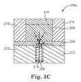
- FIG. 3Cillustrates a cross-sectional view of another embodiment of a phase change element 200 c .
- each phase change element 106is similar to phase change element 200 c .
- phase change element 200 cis a mushroom phase change element.
- Phase change element 200 cis similar to phase change element 200 a previously described and illustrated with reference to FIG. 3A , except that in phase change element 200 c , the cross-sectional width of phase change material 208 is greater than the cross-sectional width of the portion of dielectric material layer 204 that includes nanocrystals 206 and dielectric material 214 is removed. The top of dielectric material layer 204 contacts the bottom of phase change material 208 and the bottom of dielectric material 216 .
- Phase change element 200 cis programmed similarly to phase change element 200 a previously described and illustrated with reference to FIG. 3A .
- FIGS. 4-10illustrate embodiments for fabricating a phase change element, such as phase change element 200 a previously described and illustrated with reference to FIG. 3A .
- FIG. 4illustrates a cross-sectional view of one embodiment of a preprocessed wafer 230 .
- Preprocessed wafer 230includes bottom electrode 202 , dielectric material 212 , and lower wafer layers (not shown).
- the lower wafer layersinclude access devices, such as transistors or diodes, where each transistor or diode is coupled to a bottom electrode 202 .
- Bottom electrode 202includes TiN, TaN, W, Al, Ti, Ta, TiSiN, TaSiN, TiAlN, TaAlN, Cu, WN, C, or other suitable electrode material.
- Bottom electrode 202is laterally surrounded by dielectric material 212 .
- Dielectric material 212includes SiO 2 , SiO x , SiN, FSG, BPSG, BSG, or other suitable dielectric material.
- FIG. 5illustrates a cross-sectional view of one embodiment of preprocessed wafer 230 and a first dielectric material layer 204 a .
- a dielectric materialsuch as SiO 2 , SiO x , or other suitable dielectric material is deposited over preprocessed wafer 230 to provide first dielectric material layer 204 a .
- First dielectric material layer 204is deposited using chemical vapor deposition (CVD), high density plasma-chemical vapor deposition (HDP-CVD), atomic layer deposition (ALD), metal organic chemical vapor deposition (MOCVD), physical vapor deposition (PVD), jet vapor deposition (JVD), or other suitable deposition technique.
- first dielectric material layer 204 ais deposited to a thickness of between approximately 3-4 nanometers.
- first dielectric material layer 204 ais deposited to a thickness of between approximately 3-15 nanometers.
- FIG. 6illustrates a cross-sectional view of one embodiment of preprocessed wafer 230 , first dielectric material layer 204 a , and a second dielectric material layer 214 a .
- a dielectric materialsuch as SiO 2 , SiO x , SiN, FSG, BPSG, BSG, or other suitable dielectric material is deposited over first dielectric material layer 204 a to provide second dielectric material layer 214 a .
- Second dielectric material layer 214 ais deposited using CVD, HDP-CVD, ALD, MOCVD, PVD, JVD, or other suitable deposition technique. In one embodiment, second dielectric material layer 214 a is deposited to a thickness greater than the thickness of first dielectric material layer 204 a.
- FIG. 7illustrates a cross-sectional view of one embodiment of preprocessed wafer 230 , first dielectric material layer 204 a , and second dielectric material layer 214 after etching second dielectric material layer 214 a .
- Second dielectric material layer 214 ais etched to provide opening 232 exposing a portion of first dielectric material layer 204 a .
- opening 232is substantially centered above bottom electrode 202 .
- FIG. 8illustrates a cross-sectional view of one embodiment of preprocessed wafer 230 , first dielectric material layer 204 , and second dielectric material layer 214 after forming nanocrystals 206 in first dielectric material layer 204 a .
- nanocrystals 206such as Si, Ge, or other suitable nanocrystals are grown in exposed portions of first dielectric material layer 204 a .
- nanocrystals 206such as Si+, Ge+, or other suitable nanocrystals are implanted into exposed portions of first dielectric material layer 204 a .
- the nanocrystalsare implanted at an energy between approximately 1-20 keV, at a dose between approximately 10 15 -10 16 cm ⁇ 2 , and followed by rapid thermal processing (RTP) at approximately 950° C. for approximately 30 s.
- RTPrapid thermal processing
- FIG. 9illustrates a cross-sectional view of one embodiment of preprocessed wafer 230 , first dielectric material layer 204 including nanocrystals 206 , second dielectric material layer 214 , a phase change material layer 208 a , and an electrode material layer 210 a .
- a phase change materialsuch as a chalcogenide compound material or other suitable phase change material is deposited into opening 232 and over exposed portions of first dielectric material layer 204 and second dielectric material layer 214 to provide phase change material layer 208 a .
- Phase change material layer 208 ais deposited using CVD, HDP-CVD, ALD, MOCVD, PVD, JVD, or other suitable deposition technique.
- Electrode material layer 210 ais deposited using CVD, HDP-CVD, ALD, MOCVD, PVD, JVD, or other suitable deposition technique.
- FIG. 10illustrates a cross-sectional view of one embodiment of preprocessed wafer 230 , first dielectric material layer 204 including nanocrystals 206 , second dielectric material layer 214 , phase change material 208 , and a top electrode 210 .
- Electrode material layer 210 a and phase change material layer 208 aare etched to expose a portion of dielectric material layer 214 and to provide top electrode 210 and phase change material 208 .
- top electrode 210 and phase change material 208are substantially centered above bottom electrode 202 .
- second dielectric material layer 214is removed after forming nanocrystals 206 as illustrated in FIG. 8 .
- a phase change materialsuch as a chalcogenide compound material or other suitable phase change material is deposited over first dielectric material layer 204 to provide a phase change material layer.
- the phase change material layeris deposited using CVD, HDP-CVD, ALD, MOCVD, PVD, JVD, or other suitable deposition technique.
- a dielectric materialsuch as SiO 2 , SiO x , SiN, FSG, BPSG, BSG, or other suitable dielectric material is deposited over exposed portions of top electrode 210 , phase change material 208 , and first dielectric material layer 204 .
- the dielectric material layeris deposited using CVD, HDP-CVD, ALD, MOCVD, PVD, JVD, or other suitable deposition technique.
- the dielectric material layeris then planarized to expose top electrode 210 and to provide dielectric material 216 and phase change element 200 c as previously described and illustrated with reference to FIG. 3C .
- the dielectric material layeris planarized using CMP or another suitable planarization technique.
- Upper metallization layersare then fabricated, including bit lines 112 coupled to top electrodes 210 .
- FIG. 11illustrates a cross-sectional view of one embodiment of preprocessed wafer 230 and first dielectric material layer 205 after forming nanocrystals 206 in first dielectric material layer 204 a .
- nanocrystals 206such as Si, Ge, or other suitable nanocrystals are grown in first dielectric material layer 204 a .
- nanocrystals 206such as Si+, Ge+, or other suitable nanocrystals are implanted into first dielectric material layer 204 a .
- the nanocrystalsare implanted at an energy between approximately 1-20 keV, at a dose between approximately 10 15 -10 16 cm ⁇ 2 , and followed by RTP at approximately 950° C. for approximately 30 s.
- FIG. 12illustrates a cross-sectional view of one embodiment of preprocessed wafer 230 , first dielectric material layer 205 including nanocrystals 206 , and a second dielectric material layer 214 a .
- a dielectric materialsuch as SiO 2 , SiO x , SiN, FSG, BPSG, BSG, or other suitable dielectric material is deposited over first dielectric material layer 205 to provide second dielectric material layer 214 a .
- Second dielectric material layer 214 ais deposited using CVD, HDP-CVD, ALD, MOCVD, PVD, JVD, or other suitable deposition technique. In one embodiment, second dielectric material layer 214 a is deposited to a thickness greater than the thickness of first dielectric material layer 205 .
- FIG. 13illustrates a cross-sectional view of one embodiment of preprocessed wafer 230 , first dielectric material layer 205 including nanocrystals 206 , and second dielectric material layer 214 after etching second dielectric material layer 214 a .
- Second dielectric material layer 214 ais etched to provide opening 232 exposing a portion of first dielectric material layer 205 .
- opening 232is substantially centered above bottom electrode 202 .
- FIG. 14illustrates a cross-sectional view of one embodiment of preprocessed wafer 230 , first dielectric material layer 205 including nanocrystals 206 , second dielectric material layer 214 , a phase change material layer 208 a , and an electrode material layer 210 a .
- a phase change materialsuch as a chalcogenide compound material or other suitable phase change material is deposited into opening 232 and over exposed portions of first dielectric material layer 205 and second dielectric material layer 214 to provide phase change material layer 208 a .
- Phase change material layer 208 ais deposited using CVD, HDP-CVD, ALD, MOCVD, PVD, JVD, or other suitable deposition technique.
- Electrode material layer 210 ais deposited using CVD, HDP-CVD, ALD, MOCVD, PVD, JVD, or other suitable deposition technique.
- a dielectric materialsuch as SiO 2 , SiO x , SiN, FSG, BPSG, BSG, or other suitable dielectric material is deposited over exposed portions of top electrode 210 , phase change material 208 , and second dielectric material layer 214 .
- the dielectric material layeris deposited using CVD, HDP-CVD, ALD, MOCVD, PVD, JVD, or other suitable deposition technique.
- the dielectric material layeris then planarized to expose top electrode 210 and to provide dielectric material 216 and phase change element 200 b as previously described and illustrated with reference to FIG. 3B .
- the dielectric material layeris planarized using CMP or another suitable planarization technique.
- Upper metallization layersare then fabricated, including bit lines 112 coupled to top electrodes 210 .
- phase change memory elementsWhile the specific embodiments described herein substantially focused on using phase change memory elements, the present invention can be applied to any suitable type of resistive or resistivity changing memory elements.
Landscapes
- Engineering & Computer Science (AREA)
- Chemical & Material Sciences (AREA)
- Nanotechnology (AREA)
- Physics & Mathematics (AREA)
- Mathematical Physics (AREA)
- Theoretical Computer Science (AREA)
- Crystallography & Structural Chemistry (AREA)
- Manufacturing & Machinery (AREA)
- Semiconductor Memories (AREA)
Abstract
Description
Claims (23)
Priority Applications (1)
| Application Number | Priority Date | Filing Date | Title |
|---|---|---|---|
| US11/943,154US7786464B2 (en) | 2007-11-20 | 2007-11-20 | Integrated circuit having dielectric layer including nanocrystals |
Applications Claiming Priority (1)
| Application Number | Priority Date | Filing Date | Title |
|---|---|---|---|
| US11/943,154US7786464B2 (en) | 2007-11-20 | 2007-11-20 | Integrated circuit having dielectric layer including nanocrystals |
Publications (2)
| Publication Number | Publication Date |
|---|---|
| US20090127536A1 US20090127536A1 (en) | 2009-05-21 |
| US7786464B2true US7786464B2 (en) | 2010-08-31 |
Family
ID=40640943
Family Applications (1)
| Application Number | Title | Priority Date | Filing Date |
|---|---|---|---|
| US11/943,154Expired - Fee RelatedUS7786464B2 (en) | 2007-11-20 | 2007-11-20 | Integrated circuit having dielectric layer including nanocrystals |
Country Status (1)
| Country | Link |
|---|---|
| US (1) | US7786464B2 (en) |
Cited By (69)
| Publication number | Priority date | Publication date | Assignee | Title |
|---|---|---|---|---|
| US20110317470A1 (en)* | 2010-06-24 | 2011-12-29 | The Regents Of The University Of Michigan | Rectification element and method for resistive switching for non volatile memory device |
| US8374018B2 (en) | 2010-07-09 | 2013-02-12 | Crossbar, Inc. | Resistive memory using SiGe material |
| US8391049B2 (en) | 2010-09-29 | 2013-03-05 | Crossbar, Inc. | Resistor structure for a non-volatile memory device and method |
| US8394670B2 (en) | 2011-05-31 | 2013-03-12 | Crossbar, Inc. | Vertical diodes for non-volatile memory device |
| US8404553B2 (en) | 2010-08-23 | 2013-03-26 | Crossbar, Inc. | Disturb-resistant non-volatile memory device and method |
| US8441835B2 (en) | 2010-06-11 | 2013-05-14 | Crossbar, Inc. | Interface control for improved switching in RRAM |
| US8450209B2 (en) | 2010-11-05 | 2013-05-28 | Crossbar, Inc. | p+ Polysilicon material on aluminum for non-volatile memory device and method |
| US8450710B2 (en) | 2011-05-27 | 2013-05-28 | Crossbar, Inc. | Low temperature p+ silicon junction material for a non-volatile memory device |
| US8467227B1 (en) | 2010-11-04 | 2013-06-18 | Crossbar, Inc. | Hetero resistive switching material layer in RRAM device and method |
| US8492195B2 (en) | 2010-08-23 | 2013-07-23 | Crossbar, Inc. | Method for forming stackable non-volatile resistive switching memory devices |
| US8519485B2 (en) | 2010-06-11 | 2013-08-27 | Crossbar, Inc. | Pillar structure for memory device and method |
| US8558212B2 (en) | 2010-09-29 | 2013-10-15 | Crossbar, Inc. | Conductive path in switching material in a resistive random access memory device and control |
| US8659929B2 (en) | 2011-06-30 | 2014-02-25 | Crossbar, Inc. | Amorphous silicon RRAM with non-linear device and operation |
| US8658476B1 (en) | 2012-04-20 | 2014-02-25 | Crossbar, Inc. | Low temperature P+ polycrystalline silicon material for non-volatile memory device |
| US8716098B1 (en) | 2012-03-09 | 2014-05-06 | Crossbar, Inc. | Selective removal method and structure of silver in resistive switching device for a non-volatile memory device |
| US8765566B2 (en) | 2012-05-10 | 2014-07-01 | Crossbar, Inc. | Line and space architecture for a non-volatile memory device |
| US8791010B1 (en) | 2010-12-31 | 2014-07-29 | Crossbar, Inc. | Silver interconnects for stacked non-volatile memory device and method |
| US8796658B1 (en) | 2012-05-07 | 2014-08-05 | Crossbar, Inc. | Filamentary based non-volatile resistive memory device and method |
| US8809831B2 (en) | 2010-07-13 | 2014-08-19 | Crossbar, Inc. | On/off ratio for non-volatile memory device and method |
| US8815696B1 (en) | 2010-12-31 | 2014-08-26 | Crossbar, Inc. | Disturb-resistant non-volatile memory device using via-fill and etchback technique |
| US8884261B2 (en) | 2010-08-23 | 2014-11-11 | Crossbar, Inc. | Device switching using layered device structure |
| US8889521B1 (en) | 2012-09-14 | 2014-11-18 | Crossbar, Inc. | Method for silver deposition for a non-volatile memory device |
| US8930174B2 (en) | 2010-12-28 | 2015-01-06 | Crossbar, Inc. | Modeling technique for resistive random access memory (RRAM) cells |
| US8934280B1 (en) | 2013-02-06 | 2015-01-13 | Crossbar, Inc. | Capacitive discharge programming for two-terminal memory cells |
| US8947908B2 (en) | 2010-11-04 | 2015-02-03 | Crossbar, Inc. | Hetero-switching layer in a RRAM device and method |
| US8946046B1 (en) | 2012-05-02 | 2015-02-03 | Crossbar, Inc. | Guided path for forming a conductive filament in RRAM |
| US8946669B1 (en) | 2012-04-05 | 2015-02-03 | Crossbar, Inc. | Resistive memory device and fabrication methods |
| US8946673B1 (en) | 2012-08-24 | 2015-02-03 | Crossbar, Inc. | Resistive switching device structure with improved data retention for non-volatile memory device and method |
| US8982647B2 (en) | 2012-11-14 | 2015-03-17 | Crossbar, Inc. | Resistive random access memory equalization and sensing |
| US9012307B2 (en) | 2010-07-13 | 2015-04-21 | Crossbar, Inc. | Two terminal resistive switching device structure and method of fabricating |
| US9087576B1 (en) | 2012-03-29 | 2015-07-21 | Crossbar, Inc. | Low temperature fabrication method for a three-dimensional memory device and structure |
| US9112145B1 (en) | 2013-01-31 | 2015-08-18 | Crossbar, Inc. | Rectified switching of two-terminal memory via real time filament formation |
| US9153623B1 (en) | 2010-12-31 | 2015-10-06 | Crossbar, Inc. | Thin film transistor steering element for a non-volatile memory device |
| US9191000B2 (en) | 2011-07-29 | 2015-11-17 | Crossbar, Inc. | Field programmable gate array utilizing two-terminal non-volatile memory |
| US9252191B2 (en) | 2011-07-22 | 2016-02-02 | Crossbar, Inc. | Seed layer for a p+ silicon germanium material for a non-volatile memory device and method |
| US9312483B2 (en) | 2012-09-24 | 2016-04-12 | Crossbar, Inc. | Electrode structure for a non-volatile memory device and method |
| US9324942B1 (en) | 2013-01-31 | 2016-04-26 | Crossbar, Inc. | Resistive memory cell with solid state diode |
| US9401475B1 (en) | 2010-08-23 | 2016-07-26 | Crossbar, Inc. | Method for silver deposition for a non-volatile memory device |
| US9406379B2 (en) | 2013-01-03 | 2016-08-02 | Crossbar, Inc. | Resistive random access memory with non-linear current-voltage relationship |
| US9412790B1 (en) | 2012-12-04 | 2016-08-09 | Crossbar, Inc. | Scalable RRAM device architecture for a non-volatile memory device and method |
| US9460788B2 (en) | 2014-07-09 | 2016-10-04 | Crossbar, Inc. | Non-volatile memory cell utilizing volatile switching two terminal device and a MOS transistor |
| US9520557B2 (en) | 2008-10-20 | 2016-12-13 | The Regents Of The University Of Michigan | Silicon based nanoscale crossbar memory |
| US9543359B2 (en) | 2011-05-31 | 2017-01-10 | Crossbar, Inc. | Switching device having a non-linear element |
| US9564587B1 (en) | 2011-06-30 | 2017-02-07 | Crossbar, Inc. | Three-dimensional two-terminal memory with enhanced electric field and segmented interconnects |
| US9570678B1 (en) | 2010-06-08 | 2017-02-14 | Crossbar, Inc. | Resistive RAM with preferental filament formation region and methods |
| US9576616B2 (en) | 2012-10-10 | 2017-02-21 | Crossbar, Inc. | Non-volatile memory with overwrite capability and low write amplification |
| US9583701B1 (en) | 2012-08-14 | 2017-02-28 | Crossbar, Inc. | Methods for fabricating resistive memory device switching material using ion implantation |
| USRE46335E1 (en) | 2010-11-04 | 2017-03-07 | Crossbar, Inc. | Switching device having a non-linear element |
| US9601692B1 (en) | 2010-07-13 | 2017-03-21 | Crossbar, Inc. | Hetero-switching layer in a RRAM device and method |
| US9601690B1 (en) | 2011-06-30 | 2017-03-21 | Crossbar, Inc. | Sub-oxide interface layer for two-terminal memory |
| US9620206B2 (en) | 2011-05-31 | 2017-04-11 | Crossbar, Inc. | Memory array architecture with two-terminal memory cells |
| US9627443B2 (en) | 2011-06-30 | 2017-04-18 | Crossbar, Inc. | Three-dimensional oblique two-terminal memory with enhanced electric field |
| US9633723B2 (en) | 2011-06-23 | 2017-04-25 | Crossbar, Inc. | High operating speed resistive random access memory |
| US9633724B2 (en) | 2014-07-07 | 2017-04-25 | Crossbar, Inc. | Sensing a non-volatile memory device utilizing selector device holding characteristics |
| US9685483B2 (en) | 2014-07-09 | 2017-06-20 | Crossbar, Inc. | Selector-based non-volatile cell fabrication utilizing IC-foundry compatible process |
| US9685608B2 (en) | 2012-04-13 | 2017-06-20 | Crossbar, Inc. | Reduced diffusion in metal electrode for two-terminal memory |
| US9698201B2 (en) | 2014-07-09 | 2017-07-04 | Crossbar, Inc. | High density selector-based non volatile memory cell and fabrication |
| US9729155B2 (en) | 2011-07-29 | 2017-08-08 | Crossbar, Inc. | Field programmable gate array utilizing two-terminal non-volatile memory |
| US9735358B2 (en) | 2012-08-14 | 2017-08-15 | Crossbar, Inc. | Noble metal / non-noble metal electrode for RRAM applications |
| US9741765B1 (en) | 2012-08-14 | 2017-08-22 | Crossbar, Inc. | Monolithically integrated resistive memory using integrated-circuit foundry compatible processes |
| US9761635B1 (en) | 2014-03-11 | 2017-09-12 | Crossbar, Inc. | Selector device for two-terminal memory |
| US9768234B2 (en) | 2014-05-20 | 2017-09-19 | Crossbar, Inc. | Resistive memory architecture and devices |
| US10056907B1 (en) | 2011-07-29 | 2018-08-21 | Crossbar, Inc. | Field programmable gate array utilizing two-terminal non-volatile memory |
| US10096362B1 (en) | 2017-03-24 | 2018-10-09 | Crossbar, Inc. | Switching block configuration bit comprising a non-volatile memory cell |
| US10115819B2 (en) | 2015-05-29 | 2018-10-30 | Crossbar, Inc. | Recessed high voltage metal oxide semiconductor transistor for RRAM cell |
| US10211397B1 (en) | 2014-07-07 | 2019-02-19 | Crossbar, Inc. | Threshold voltage tuning for a volatile selection device |
| US10290801B2 (en) | 2014-02-07 | 2019-05-14 | Crossbar, Inc. | Scalable silicon based resistive memory device |
| US11056645B2 (en)* | 2018-12-20 | 2021-07-06 | Samsung Electronics Co., Ltd. | Vertical memory devices |
| US11068620B2 (en) | 2012-11-09 | 2021-07-20 | Crossbar, Inc. | Secure circuit integrated with memory layer |
Families Citing this family (6)
| Publication number | Priority date | Publication date | Assignee | Title |
|---|---|---|---|---|
| US20100123117A1 (en)* | 2008-11-19 | 2010-05-20 | Seagate Technology Llc | Non volatile memory cells including a filament growth layer and methods of forming the same |
| CN101789492B (en)* | 2010-03-01 | 2011-12-07 | 中国科学院半导体研究所 | Preparation method of plane phase change memory |
| US9082954B2 (en)* | 2010-09-24 | 2015-07-14 | Macronix International Co., Ltd. | PCRAM with current flowing laterally relative to axis defined by electrodes |
| GB2515567A (en)* | 2013-06-28 | 2014-12-31 | Ibm | Phase-Change memory cells |
| US9627612B2 (en)* | 2014-02-27 | 2017-04-18 | International Business Machines Corporation | Metal nitride keyhole or spacer phase change memory cell structures |
| US12268103B2 (en)* | 2022-06-09 | 2025-04-01 | Taiwan Semiconductor Manufacturing Company Limited | Phase change material switch with improved thermal confinement and methods for forming the same |
Citations (5)
| Publication number | Priority date | Publication date | Assignee | Title |
|---|---|---|---|---|
| US6329666B1 (en)* | 1996-10-02 | 2001-12-11 | Micron Technology, Inc. | Controllable ovonic phase-change semiconductor memory device and methods of fabricating the same |
| US20030103406A1 (en)* | 1999-01-14 | 2003-06-05 | Tran Hieu Van | Digital multilevel memory system having multistage autozero sensing |
| US20050158950A1 (en) | 2002-12-19 | 2005-07-21 | Matrix Semiconductor, Inc. | Non-volatile memory cell comprising a dielectric layer and a phase change material in series |
| US20050173691A1 (en) | 2004-02-09 | 2005-08-11 | Macronix International Co., Ltd. | Structure for phase change memory and the method of forming same |
| US20070018342A1 (en)* | 2005-07-20 | 2007-01-25 | Micron Technology, Inc. | Devices with nanocrystals and methods of formation |
- 2007
- 2007-11-20USUS11/943,154patent/US7786464B2/ennot_activeExpired - Fee Related
Patent Citations (5)
| Publication number | Priority date | Publication date | Assignee | Title |
|---|---|---|---|---|
| US6329666B1 (en)* | 1996-10-02 | 2001-12-11 | Micron Technology, Inc. | Controllable ovonic phase-change semiconductor memory device and methods of fabricating the same |
| US20030103406A1 (en)* | 1999-01-14 | 2003-06-05 | Tran Hieu Van | Digital multilevel memory system having multistage autozero sensing |
| US20050158950A1 (en) | 2002-12-19 | 2005-07-21 | Matrix Semiconductor, Inc. | Non-volatile memory cell comprising a dielectric layer and a phase change material in series |
| US20050173691A1 (en) | 2004-02-09 | 2005-08-11 | Macronix International Co., Ltd. | Structure for phase change memory and the method of forming same |
| US20070018342A1 (en)* | 2005-07-20 | 2007-01-25 | Micron Technology, Inc. | Devices with nanocrystals and methods of formation |
Non-Patent Citations (6)
| Title |
|---|
| "Chemical Vapor Deposition of Ge nanocrystals on SiO2", T. Baron, et al., 2003 American Institute of Physics. (3 pgs.). |
| "Highly Reliable 50nm Contact Cell Technology for 256Mb PRAM", S.J. Ahn, et al., 2005 Symposium on VLSI Technology Digest of Technical Papers. (2 pgs.). |
| "How Far will Silicon Nanocrystals Push the Scaling Limits of NVMs Technologies?", B. De Salvo, et al., 2003 IEEE (4 pgs.). |
| "Influence of the Chemical Properties of the Substrate on Silicon Quantum Dot Nucleation", F. Mazen, et al., Journal of the Electrochemical Society, 2003. (6 pgs.). |
| "Microstructure and Electrical Properties of Ge- and Si-Nanoclusters in Implanted Gate Oxide for Embedded Memory Applications", K. H. Stegemann, et al. (7 pgs.). |
| "Novel One-Mask Self-heating Pillar Phase Change Memory", T. D. Happ, et al., 2006 Symposium on VLSI Technology Digest of Technical Papers. (2 pgs.). |
Cited By (103)
| Publication number | Priority date | Publication date | Assignee | Title |
|---|---|---|---|---|
| US9520557B2 (en) | 2008-10-20 | 2016-12-13 | The Regents Of The University Of Michigan | Silicon based nanoscale crossbar memory |
| US9570678B1 (en) | 2010-06-08 | 2017-02-14 | Crossbar, Inc. | Resistive RAM with preferental filament formation region and methods |
| US8993397B2 (en) | 2010-06-11 | 2015-03-31 | Crossbar, Inc. | Pillar structure for memory device and method |
| US8599601B2 (en) | 2010-06-11 | 2013-12-03 | Crossbar, Inc. | Interface control for improved switching in RRAM |
| US8441835B2 (en) | 2010-06-11 | 2013-05-14 | Crossbar, Inc. | Interface control for improved switching in RRAM |
| US8519485B2 (en) | 2010-06-11 | 2013-08-27 | Crossbar, Inc. | Pillar structure for memory device and method |
| US8351241B2 (en)* | 2010-06-24 | 2013-01-08 | The Regents Of The University Of Michigan | Rectification element and method for resistive switching for non volatile memory device |
| US8750020B2 (en) | 2010-06-24 | 2014-06-10 | The Regents Of The University Of Michigan | Resistive switching for non volatile memory device using an integrated breakdown element |
| US9048658B2 (en) | 2010-06-24 | 2015-06-02 | The Regents Of The University Of Michigan | Resistive switching for non volatile memory device using an integrated breakdown element |
| US20110317470A1 (en)* | 2010-06-24 | 2011-12-29 | The Regents Of The University Of Michigan | Rectification element and method for resistive switching for non volatile memory device |
| US9627614B2 (en) | 2010-06-24 | 2017-04-18 | The Regents Of The University Of Michigan | Resistive switching for non volatile memory device using an integrated breakdown element |
| US8750019B2 (en) | 2010-07-09 | 2014-06-10 | Crossbar, Inc. | Resistive memory using SiGe material |
| US9036400B2 (en) | 2010-07-09 | 2015-05-19 | Crossbar, Inc. | Method and structure of monolithically integrated IC and resistive memory using IC foundry-compatible processes |
| US8374018B2 (en) | 2010-07-09 | 2013-02-12 | Crossbar, Inc. | Resistive memory using SiGe material |
| US9012307B2 (en) | 2010-07-13 | 2015-04-21 | Crossbar, Inc. | Two terminal resistive switching device structure and method of fabricating |
| US8809831B2 (en) | 2010-07-13 | 2014-08-19 | Crossbar, Inc. | On/off ratio for non-volatile memory device and method |
| US9755143B2 (en) | 2010-07-13 | 2017-09-05 | Crossbar, Inc. | On/off ratio for nonvolatile memory device and method |
| US9601692B1 (en) | 2010-07-13 | 2017-03-21 | Crossbar, Inc. | Hetero-switching layer in a RRAM device and method |
| US8648327B2 (en) | 2010-08-23 | 2014-02-11 | Crossbar, Inc. | Stackable non-volatile resistive switching memory devices |
| US9590013B2 (en) | 2010-08-23 | 2017-03-07 | Crossbar, Inc. | Device switching using layered device structure |
| US9401475B1 (en) | 2010-08-23 | 2016-07-26 | Crossbar, Inc. | Method for silver deposition for a non-volatile memory device |
| US9035276B2 (en) | 2010-08-23 | 2015-05-19 | Crossbar, Inc. | Stackable non-volatile resistive switching memory device |
| US9412789B1 (en) | 2010-08-23 | 2016-08-09 | Crossbar, Inc. | Stackable non-volatile resistive switching memory device and method of fabricating the same |
| US10224370B2 (en) | 2010-08-23 | 2019-03-05 | Crossbar, Inc. | Device switching using layered device structure |
| US8404553B2 (en) | 2010-08-23 | 2013-03-26 | Crossbar, Inc. | Disturb-resistant non-volatile memory device and method |
| US8492195B2 (en) | 2010-08-23 | 2013-07-23 | Crossbar, Inc. | Method for forming stackable non-volatile resistive switching memory devices |
| US8884261B2 (en) | 2010-08-23 | 2014-11-11 | Crossbar, Inc. | Device switching using layered device structure |
| US8912523B2 (en) | 2010-09-29 | 2014-12-16 | Crossbar, Inc. | Conductive path in switching material in a resistive random access memory device and control |
| US9129887B2 (en) | 2010-09-29 | 2015-09-08 | Crossbar, Inc. | Resistor structure for a non-volatile memory device and method |
| US8558212B2 (en) | 2010-09-29 | 2013-10-15 | Crossbar, Inc. | Conductive path in switching material in a resistive random access memory device and control |
| US8391049B2 (en) | 2010-09-29 | 2013-03-05 | Crossbar, Inc. | Resistor structure for a non-volatile memory device and method |
| US8659933B2 (en) | 2010-11-04 | 2014-02-25 | Crossbar, Inc. | Hereto resistive switching material layer in RRAM device and method |
| US8947908B2 (en) | 2010-11-04 | 2015-02-03 | Crossbar, Inc. | Hetero-switching layer in a RRAM device and method |
| USRE46335E1 (en) | 2010-11-04 | 2017-03-07 | Crossbar, Inc. | Switching device having a non-linear element |
| US8467227B1 (en) | 2010-11-04 | 2013-06-18 | Crossbar, Inc. | Hetero resistive switching material layer in RRAM device and method |
| US8450209B2 (en) | 2010-11-05 | 2013-05-28 | Crossbar, Inc. | p+ Polysilicon material on aluminum for non-volatile memory device and method |
| US8930174B2 (en) | 2010-12-28 | 2015-01-06 | Crossbar, Inc. | Modeling technique for resistive random access memory (RRAM) cells |
| US9153623B1 (en) | 2010-12-31 | 2015-10-06 | Crossbar, Inc. | Thin film transistor steering element for a non-volatile memory device |
| US9831289B2 (en) | 2010-12-31 | 2017-11-28 | Crossbar, Inc. | Disturb-resistant non-volatile memory device using via-fill and etchback technique |
| US8815696B1 (en) | 2010-12-31 | 2014-08-26 | Crossbar, Inc. | Disturb-resistant non-volatile memory device using via-fill and etchback technique |
| US8791010B1 (en) | 2010-12-31 | 2014-07-29 | Crossbar, Inc. | Silver interconnects for stacked non-volatile memory device and method |
| US8450710B2 (en) | 2011-05-27 | 2013-05-28 | Crossbar, Inc. | Low temperature p+ silicon junction material for a non-volatile memory device |
| US9620206B2 (en) | 2011-05-31 | 2017-04-11 | Crossbar, Inc. | Memory array architecture with two-terminal memory cells |
| US9543359B2 (en) | 2011-05-31 | 2017-01-10 | Crossbar, Inc. | Switching device having a non-linear element |
| US8394670B2 (en) | 2011-05-31 | 2013-03-12 | Crossbar, Inc. | Vertical diodes for non-volatile memory device |
| US9633723B2 (en) | 2011-06-23 | 2017-04-25 | Crossbar, Inc. | High operating speed resistive random access memory |
| US9564587B1 (en) | 2011-06-30 | 2017-02-07 | Crossbar, Inc. | Three-dimensional two-terminal memory with enhanced electric field and segmented interconnects |
| US9601690B1 (en) | 2011-06-30 | 2017-03-21 | Crossbar, Inc. | Sub-oxide interface layer for two-terminal memory |
| US9627443B2 (en) | 2011-06-30 | 2017-04-18 | Crossbar, Inc. | Three-dimensional oblique two-terminal memory with enhanced electric field |
| US9570683B1 (en) | 2011-06-30 | 2017-02-14 | Crossbar, Inc. | Three-dimensional two-terminal memory with enhanced electric field and segmented interconnects |
| US8659929B2 (en) | 2011-06-30 | 2014-02-25 | Crossbar, Inc. | Amorphous silicon RRAM with non-linear device and operation |
| US9252191B2 (en) | 2011-07-22 | 2016-02-02 | Crossbar, Inc. | Seed layer for a p+ silicon germanium material for a non-volatile memory device and method |
| US9729155B2 (en) | 2011-07-29 | 2017-08-08 | Crossbar, Inc. | Field programmable gate array utilizing two-terminal non-volatile memory |
| US9191000B2 (en) | 2011-07-29 | 2015-11-17 | Crossbar, Inc. | Field programmable gate array utilizing two-terminal non-volatile memory |
| US10056907B1 (en) | 2011-07-29 | 2018-08-21 | Crossbar, Inc. | Field programmable gate array utilizing two-terminal non-volatile memory |
| US8716098B1 (en) | 2012-03-09 | 2014-05-06 | Crossbar, Inc. | Selective removal method and structure of silver in resistive switching device for a non-volatile memory device |
| US9087576B1 (en) | 2012-03-29 | 2015-07-21 | Crossbar, Inc. | Low temperature fabrication method for a three-dimensional memory device and structure |
| US9673255B2 (en) | 2012-04-05 | 2017-06-06 | Crossbar, Inc. | Resistive memory device and fabrication methods |
| US8946669B1 (en) | 2012-04-05 | 2015-02-03 | Crossbar, Inc. | Resistive memory device and fabrication methods |
| US9685608B2 (en) | 2012-04-13 | 2017-06-20 | Crossbar, Inc. | Reduced diffusion in metal electrode for two-terminal memory |
| US10910561B1 (en) | 2012-04-13 | 2021-02-02 | Crossbar, Inc. | Reduced diffusion in metal electrode for two-terminal memory |
| US9793474B2 (en) | 2012-04-20 | 2017-10-17 | Crossbar, Inc. | Low temperature P+ polycrystalline silicon material for non-volatile memory device |
| US8658476B1 (en) | 2012-04-20 | 2014-02-25 | Crossbar, Inc. | Low temperature P+ polycrystalline silicon material for non-volatile memory device |
| US8946046B1 (en) | 2012-05-02 | 2015-02-03 | Crossbar, Inc. | Guided path for forming a conductive filament in RRAM |
| US9972778B2 (en) | 2012-05-02 | 2018-05-15 | Crossbar, Inc. | Guided path for forming a conductive filament in RRAM |
| US9385319B1 (en) | 2012-05-07 | 2016-07-05 | Crossbar, Inc. | Filamentary based non-volatile resistive memory device and method |
| US8796658B1 (en) | 2012-05-07 | 2014-08-05 | Crossbar, Inc. | Filamentary based non-volatile resistive memory device and method |
| US8765566B2 (en) | 2012-05-10 | 2014-07-01 | Crossbar, Inc. | Line and space architecture for a non-volatile memory device |
| US9583701B1 (en) | 2012-08-14 | 2017-02-28 | Crossbar, Inc. | Methods for fabricating resistive memory device switching material using ion implantation |
| US10096653B2 (en) | 2012-08-14 | 2018-10-09 | Crossbar, Inc. | Monolithically integrated resistive memory using integrated-circuit foundry compatible processes |
| US9741765B1 (en) | 2012-08-14 | 2017-08-22 | Crossbar, Inc. | Monolithically integrated resistive memory using integrated-circuit foundry compatible processes |
| US9735358B2 (en) | 2012-08-14 | 2017-08-15 | Crossbar, Inc. | Noble metal / non-noble metal electrode for RRAM applications |
| US8946673B1 (en) | 2012-08-24 | 2015-02-03 | Crossbar, Inc. | Resistive switching device structure with improved data retention for non-volatile memory device and method |
| US8889521B1 (en) | 2012-09-14 | 2014-11-18 | Crossbar, Inc. | Method for silver deposition for a non-volatile memory device |
| US9312483B2 (en) | 2012-09-24 | 2016-04-12 | Crossbar, Inc. | Electrode structure for a non-volatile memory device and method |
| US9576616B2 (en) | 2012-10-10 | 2017-02-21 | Crossbar, Inc. | Non-volatile memory with overwrite capability and low write amplification |
| US12254124B1 (en) | 2012-11-09 | 2025-03-18 | Crossbar, Inc. | Secure circuit integrated with memory layer |
| US11836277B2 (en) | 2012-11-09 | 2023-12-05 | Crossbar, Inc. | Secure circuit integrated with memory layer |
| US11068620B2 (en) | 2012-11-09 | 2021-07-20 | Crossbar, Inc. | Secure circuit integrated with memory layer |
| US8982647B2 (en) | 2012-11-14 | 2015-03-17 | Crossbar, Inc. | Resistive random access memory equalization and sensing |
| US9412790B1 (en) | 2012-12-04 | 2016-08-09 | Crossbar, Inc. | Scalable RRAM device architecture for a non-volatile memory device and method |
| US9406379B2 (en) | 2013-01-03 | 2016-08-02 | Crossbar, Inc. | Resistive random access memory with non-linear current-voltage relationship |
| US9112145B1 (en) | 2013-01-31 | 2015-08-18 | Crossbar, Inc. | Rectified switching of two-terminal memory via real time filament formation |
| US9324942B1 (en) | 2013-01-31 | 2016-04-26 | Crossbar, Inc. | Resistive memory cell with solid state diode |
| US8934280B1 (en) | 2013-02-06 | 2015-01-13 | Crossbar, Inc. | Capacitive discharge programming for two-terminal memory cells |
| US10290801B2 (en) | 2014-02-07 | 2019-05-14 | Crossbar, Inc. | Scalable silicon based resistive memory device |
| US9847130B1 (en) | 2014-03-11 | 2017-12-19 | Crossbar, Inc. | Selector device for two-terminal memory |
| US9761635B1 (en) | 2014-03-11 | 2017-09-12 | Crossbar, Inc. | Selector device for two-terminal memory |
| US11776626B2 (en) | 2014-03-11 | 2023-10-03 | Crossbar, Inc. | Selector device for two-terminal memory |
| US10121540B1 (en) | 2014-03-11 | 2018-11-06 | Crossbar, Inc. | Selector device for two-terminal memory |
| US10964388B2 (en) | 2014-03-11 | 2021-03-30 | Crossbar, Inc. | Selector device for two-terminal memory |
| US9768234B2 (en) | 2014-05-20 | 2017-09-19 | Crossbar, Inc. | Resistive memory architecture and devices |
| US9633724B2 (en) | 2014-07-07 | 2017-04-25 | Crossbar, Inc. | Sensing a non-volatile memory device utilizing selector device holding characteristics |
| US10211397B1 (en) | 2014-07-07 | 2019-02-19 | Crossbar, Inc. | Threshold voltage tuning for a volatile selection device |
| US10079060B2 (en) | 2014-07-07 | 2018-09-18 | Crossbar, Inc. | Sensing a non-volatile memory device utilizing selector device holding characteristics |
| US10210929B1 (en) | 2014-07-09 | 2019-02-19 | Crossbar, Inc. | Non-volatile memory cell utilizing volatile switching two terminal device and a MOS transistor |
| US9460788B2 (en) | 2014-07-09 | 2016-10-04 | Crossbar, Inc. | Non-volatile memory cell utilizing volatile switching two terminal device and a MOS transistor |
| US9698201B2 (en) | 2014-07-09 | 2017-07-04 | Crossbar, Inc. | High density selector-based non volatile memory cell and fabrication |
| US9685483B2 (en) | 2014-07-09 | 2017-06-20 | Crossbar, Inc. | Selector-based non-volatile cell fabrication utilizing IC-foundry compatible process |
| US10115819B2 (en) | 2015-05-29 | 2018-10-30 | Crossbar, Inc. | Recessed high voltage metal oxide semiconductor transistor for RRAM cell |
| US10541025B2 (en) | 2017-03-24 | 2020-01-21 | Crossbar, Inc. | Switching block configuration bit comprising a non-volatile memory cell |
| US10096362B1 (en) | 2017-03-24 | 2018-10-09 | Crossbar, Inc. | Switching block configuration bit comprising a non-volatile memory cell |
| US11056645B2 (en)* | 2018-12-20 | 2021-07-06 | Samsung Electronics Co., Ltd. | Vertical memory devices |
Also Published As
| Publication number | Publication date |
|---|---|
| US20090127536A1 (en) | 2009-05-21 |
Similar Documents
| Publication | Publication Date | Title |
|---|---|---|
| US7786464B2 (en) | Integrated circuit having dielectric layer including nanocrystals | |
| US7545668B2 (en) | Mushroom phase change memory having a multilayer electrode | |
| US8284596B2 (en) | Integrated circuit including an array of diodes coupled to a layer of resistance changing material | |
| US7863593B2 (en) | Integrated circuit including force-filled resistivity changing material | |
| US8208294B2 (en) | Resistive memory cell accessed using two bit lines | |
| US7838860B2 (en) | Integrated circuit including vertical diode | |
| US7869257B2 (en) | Integrated circuit including diode memory cells | |
| US9064794B2 (en) | Integrated circuit including vertical diode | |
| US7888665B2 (en) | Integrated circuit including memory cell having cup-shaped electrode interface | |
| US8189372B2 (en) | Integrated circuit including electrode having recessed portion | |
| US20080265239A1 (en) | Integrated circuit including spacer material layer | |
| US8039299B2 (en) | Method for fabricating an integrated circuit including resistivity changing material having a planarized surface | |
| US8003971B2 (en) | Integrated circuit including memory element doped with dielectric material | |
| US20090185411A1 (en) | Integrated circuit including diode memory cells | |
| US7545019B2 (en) | Integrated circuit including logic portion and memory portion | |
| US7671354B2 (en) | Integrated circuit including spacer defined electrode | |
| US7745812B2 (en) | Integrated circuit including vertical diode | |
| US20080316793A1 (en) | Integrated circuit including contact contacting bottom and sidewall of electrode | |
| US8189374B2 (en) | Memory device including an electrode having an outer portion with greater resistivity | |
| US7671353B2 (en) | Integrated circuit having contact including material between sidewalls | |
| US7696510B2 (en) | Integrated circuit including memory having reduced cross talk | |
| US7829879B2 (en) | Integrated circuit including U-shaped access device | |
| US20080315171A1 (en) | Integrated circuit including vertical diode | |
| US7679074B2 (en) | Integrated circuit having multilayer electrode | |
| US7994536B2 (en) | Integrated circuit including U-shaped access device |
Legal Events
| Date | Code | Title | Description |
|---|---|---|---|
| AS | Assignment | Owner name:INFINEON TECHNOLOGIES NORTH AMERICA CORP., CALIFOR Free format text:ASSIGNMENT OF ASSIGNORS INTEREST;ASSIGNOR:NIRSCHL, THOMAS;REEL/FRAME:020231/0013 Effective date:20071108 Owner name:INFINEON TECHNOLOGIES AG, GERMANY Free format text:ASSIGNMENT OF ASSIGNORS INTEREST;ASSIGNOR:KAKOSCHKE, RONALD;REEL/FRAME:020231/0041 Effective date:20071108 | |
| AS | Assignment | Owner name:INFINEON TECHNOLOGIES AG, GERMANY Free format text:ASSIGNMENT OF ASSIGNORS INTEREST;ASSIGNOR:INFINEON TECHNOLOGIES NORTH AMERICA CORP.;REEL/FRAME:020372/0515 Effective date:20080114 Owner name:INFINEON TECHNOLOGIES AG,GERMANY Free format text:ASSIGNMENT OF ASSIGNORS INTEREST;ASSIGNOR:INFINEON TECHNOLOGIES NORTH AMERICA CORP.;REEL/FRAME:020372/0515 Effective date:20080114 | |
| FEPP | Fee payment procedure | Free format text:PAYOR NUMBER ASSIGNED (ORIGINAL EVENT CODE: ASPN); ENTITY STATUS OF PATENT OWNER: LARGE ENTITY | |
| STCF | Information on status: patent grant | Free format text:PATENTED CASE | |
| FPAY | Fee payment | Year of fee payment:4 | |
| MAFP | Maintenance fee payment | Free format text:PAYMENT OF MAINTENANCE FEE, 8TH YEAR, LARGE ENTITY (ORIGINAL EVENT CODE: M1552) Year of fee payment:8 | |
| FEPP | Fee payment procedure | Free format text:MAINTENANCE FEE REMINDER MAILED (ORIGINAL EVENT CODE: REM.); ENTITY STATUS OF PATENT OWNER: LARGE ENTITY | |
| LAPS | Lapse for failure to pay maintenance fees | Free format text:PATENT EXPIRED FOR FAILURE TO PAY MAINTENANCE FEES (ORIGINAL EVENT CODE: EXP.); ENTITY STATUS OF PATENT OWNER: LARGE ENTITY | |
| STCH | Information on status: patent discontinuation | Free format text:PATENT EXPIRED DUE TO NONPAYMENT OF MAINTENANCE FEES UNDER 37 CFR 1.362 | |
| FP | Lapsed due to failure to pay maintenance fee | Effective date:20220831 |