US7786463B2 - Non-volatile multi-bit memory with programmable capacitance - Google Patents
Non-volatile multi-bit memory with programmable capacitanceDownload PDFInfo
- Publication number
- US7786463B2 US7786463B2US12/123,685US12368508AUS7786463B2US 7786463 B2US7786463 B2US 7786463B2US 12368508 AUS12368508 AUS 12368508AUS 7786463 B2US7786463 B2US 7786463B2
- Authority
- US
- United States
- Prior art keywords
- solid electrolyte
- electrolyte cell
- anode
- memory unit
- bit memory
- Prior art date
- Legal status (The legal status is an assumption and is not a legal conclusion. Google has not performed a legal analysis and makes no representation as to the accuracy of the status listed.)
- Expired - Fee Related, expires
Links
Images


Classifications
- H—ELECTRICITY
- H10—SEMICONDUCTOR DEVICES; ELECTRIC SOLID-STATE DEVICES NOT OTHERWISE PROVIDED FOR
- H10N—ELECTRIC SOLID-STATE DEVICES NOT OTHERWISE PROVIDED FOR
- H10N70/00—Solid-state devices having no potential barriers, and specially adapted for rectifying, amplifying, oscillating or switching
- H10N70/011—Manufacture or treatment of multistable switching devices
- H10N70/041—Modification of switching materials after formation, e.g. doping
- H10N70/046—Modification of switching materials after formation, e.g. doping by diffusion, e.g. photo-dissolution
- H—ELECTRICITY
- H10—SEMICONDUCTOR DEVICES; ELECTRIC SOLID-STATE DEVICES NOT OTHERWISE PROVIDED FOR
- H10N—ELECTRIC SOLID-STATE DEVICES NOT OTHERWISE PROVIDED FOR
- H10N70/00—Solid-state devices having no potential barriers, and specially adapted for rectifying, amplifying, oscillating or switching
- H10N70/20—Multistable switching devices, e.g. memristors
- H10N70/24—Multistable switching devices, e.g. memristors based on migration or redistribution of ionic species, e.g. anions, vacancies
- H10N70/245—Multistable switching devices, e.g. memristors based on migration or redistribution of ionic species, e.g. anions, vacancies the species being metal cations, e.g. programmable metallization cells
- H—ELECTRICITY
- H10—SEMICONDUCTOR DEVICES; ELECTRIC SOLID-STATE DEVICES NOT OTHERWISE PROVIDED FOR
- H10N—ELECTRIC SOLID-STATE DEVICES NOT OTHERWISE PROVIDED FOR
- H10N70/00—Solid-state devices having no potential barriers, and specially adapted for rectifying, amplifying, oscillating or switching
- H10N70/20—Multistable switching devices, e.g. memristors
- H10N70/253—Multistable switching devices, e.g. memristors having three or more electrodes, e.g. transistor-like devices
- H—ELECTRICITY
- H10—SEMICONDUCTOR DEVICES; ELECTRIC SOLID-STATE DEVICES NOT OTHERWISE PROVIDED FOR
- H10N—ELECTRIC SOLID-STATE DEVICES NOT OTHERWISE PROVIDED FOR
- H10N70/00—Solid-state devices having no potential barriers, and specially adapted for rectifying, amplifying, oscillating or switching
- H10N70/801—Constructional details of multistable switching devices
- H10N70/841—Electrodes
- H10N70/8416—Electrodes adapted for supplying ionic species
- H—ELECTRICITY
- H10—SEMICONDUCTOR DEVICES; ELECTRIC SOLID-STATE DEVICES NOT OTHERWISE PROVIDED FOR
- H10N—ELECTRIC SOLID-STATE DEVICES NOT OTHERWISE PROVIDED FOR
- H10N70/00—Solid-state devices having no potential barriers, and specially adapted for rectifying, amplifying, oscillating or switching
- H10N70/801—Constructional details of multistable switching devices
- H10N70/881—Switching materials
- H10N70/882—Compounds of sulfur, selenium or tellurium, e.g. chalcogenides
- H10N70/8825—Selenides, e.g. GeSe
- G—PHYSICS
- G11—INFORMATION STORAGE
- G11C—STATIC STORES
- G11C16/00—Erasable programmable read-only memories
- G11C16/02—Erasable programmable read-only memories electrically programmable
- G11C16/04—Erasable programmable read-only memories electrically programmable using variable threshold transistors, e.g. FAMOS
- G11C16/0466—Erasable programmable read-only memories electrically programmable using variable threshold transistors, e.g. FAMOS comprising cells with charge storage in an insulating layer, e.g. metal-nitride-oxide-silicon [MNOS], silicon-oxide-nitride-oxide-silicon [SONOS]
- G11C16/0475—Erasable programmable read-only memories electrically programmable using variable threshold transistors, e.g. FAMOS comprising cells with charge storage in an insulating layer, e.g. metal-nitride-oxide-silicon [MNOS], silicon-oxide-nitride-oxide-silicon [SONOS] comprising two or more independent storage sites which store independent data
Definitions
- Nonvolatile memoryis a type of memory that retains stored data when power is removed from the memory.
- nonvolatile memoriesincluding e.g., flash memory.
- Flash memory cellsmake use of a floating-gate covered with an insulating layer. There is also a control gate which overlays the insulating layer. Below the floating gate is another insulating layer sandwiched between the floating gate and the cell substrate. This insulating layer is an oxide layer and is often referred to as the gate oxide or tunnel oxide.
- the substratecontains doped source and drain regions, with a channel region disposed between the source and drain regions.
- the floating-gate transistorsgenerally include n-channel floating-gate field-effect transistors, but may also include p-channel floating-gate field-effect transistors. Access operations are carried out by applying biases to the transistor.
- a charged floating gatemay represent a logical “1” while a non-charged floating gate may represent a logical “0.”
- a flash memory cellmay be programmed to a desired state by first erasing the cell to a logical “0” and, if necessary, writing the cell to a logical “1.”
- flash memory devicesare organized so that a write operation can target a specific cell while an erase operation affects an entire block of cells. Changing any portion of one block therefore requires erasing the entire block and writing those bits in the block which correspond to a logical “1”.
- the present disclosurerelates to non-volatile multi-bit memory having a programmable capacitance.
- the multi-bit memorycan have its threshold voltage changed by changing the capacitance of each solid electrolyte cell of the memory gate stack.
- One approach to changing the capacitance each solid electrolyte cell of the memory gate stackis to utilize electrochemical reactions to build or break metal dendrites in each solid electrolyte cell within the gate stack.
- Particular multi-bit memory unit architectures including the solid electrolyte cellsare disclosed.
- a multi-bit memory unitincludes a substrate having a source region and a drain region.
- a first insulating layeris over the substrate.
- a first solid electrolyte cellis over the insulating layer and has a capacitance that is controllable between at least two states and is proximate the source region.
- a second solid electrolyte cellis over the insulating layer and has a capacitance that is controllable between at least two states and is proximate the drain region.
- An insulating elementisolates the first solid electrolyte cell from the second solid electrolyte cell.
- a first anodeis electrically coupled to the first solid electrolyte cell. The first solid electrolyte cell is between the anode and the insulating layer.
- a second anodeis electrically coupled to the second solid electrolyte cell.
- the second solid electrolyte cellis between the anode and the insulating layer.
- a gate contact layeris over the substrate and between the source region and drain region and in electrical connection with the first anode and the second anode.
- the gate contact layeris electrically coupled to a voltage source.
- a multi-bit memory unitin another particular embodiment, includes a substrate having a source region and a drain region. An insulating layer is over the substrate. A first solid electrolyte cell is disposed between a first anode and a first barrier layer. The first solid electrolyte cell is over the insulating layer and has a capacitance that is controllable between at least two states. A second solid electrolyte cell is disposed between a second anode and a second barrier layer. The second solid electrolyte cell is over the insulating layer and has a capacitance that is controllable between at least two states. A gate contact layer is over the substrate and between the source region and drain region and in electrical connection with the first anode and the second anode.
- the gate contact layeris electrically coupled to a voltage source.
- the first solid electrolyte cellis located closer to the source region than the second solid electrolyte cell and the second solid electrolyte cell is located closer to the drain region than the first solid electrolyte cell.
- the first solid electrolyte cellis electrically isolated from the second solid electrolyte cell.
- a multi-bit non-volatile memory unitin another embodiment, includes a substrate including a source region and a drain region. The source region is electrically coupled to a source voltage source and the drain region is electrically coupled to a drain voltage source. An insulating layer is over the substrate. A first solid electrolyte cell is disposed between a first electrochemically active anode and a first barrier layer. The first solid electrolyte cell is over the insulating layer. The first solid electrolyte cell has a capacitance that is controllable between at least two states. A second solid electrolyte cell is disposed between a second electrochemically active anode and a second barrier layer. The second solid electrolyte cell is over the insulating layer.
- the second solid electrolyte cellhas a capacitance that is controllable between at least two states.
- a gate contact layeris over the substrate and between the source region and drain region and in electrical connection with the first electrochemically active anode and the second electrochemically active anode.
- the gate contact layeris electrically coupled to a gate voltage source.
- the first solid electrolyte cellis located closer to the source region than the second solid electrolyte cell and the second solid electrolyte cell is located closer to the drain region than the first solid electrolyte cell.
- the first solid electrolyte cell, first anode and first barrier layerare electrically isolated from the second solid electrolyte cell, second anode and second barrier layer.
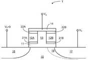
- FIG. 1is a schematic cross-sectional diagram of an illustrative non-volatile multi-bit memory unit having programmable capacitance
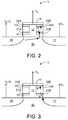
- FIG. 2is a schematic cross-sectional diagram of an exemplary non-volatile multi-bit memory unit shown in FIG. 1 during a programming operation of one solid electrolyte cell;
- FIG. 3is a schematic cross-sectional diagram of an exemplary non-volatile multi-bit memory unit shown in FIG. 1 during an erase operation of the solid electrolyte cell programmed in FIG. 2 ;
- FIG. 4is a schematic cross-sectional diagram of an exemplary non-volatile multi-bit memory unit shown in FIG. 1 during a programming operation of another solid electrolyte cell;
- FIG. 5is a schematic cross-sectional diagram of an exemplary non-volatile multi-bit memory unit shown in FIG. 1 during an erase operation of the solid electrolyte cell programmed in FIG. 4 ;
- FIG. 6is a schematic cross-sectional diagram of an exemplary non-volatile memory unit shown in FIG. 1 during a read operation of one solid electrolyte cell.
- the present disclosurerelates to non-volatile multi-bit memory having a programmable capacitance.
- the multi-bit memorycan have its threshold voltage changed by changing the capacitance of each solid electrolyte cell of the memory gate stack.
- One approach to changing the capacitance, resistance, or conductivity (hereinafter referred to as capacitance) of each solid electrolyte cell of the memory gate stackis to utilize electrochemical reactions to build or break metal dendrites in each solid electrolyte cell within the gate stack.
- capacitancecapacitance
- Particular multi-bit memory unit architectures including the solid electrolyte cellsare disclosed.
- Thesesinclude single transistors that have two programmable solid electrolyte cells that are physically and electrically separated from each other and each cell can be programmed to be either conductive or non-conductive, which changes the capacitance of the gate stack. The channel current will thus be changed by this capacitance change.
- Each cell or bitcan be programmed independently of each other to store two data states in a single gate stack or transistor.
- the non-volatile memory unitsare described herein can replace traditional memory units such as, for example, FLASH memory. While the present disclosure is not so limited, an appreciation of various aspects of the disclosure will be gained through a discussion of the examples provided below.
- FIG. 1is a schematic cross-sectional diagram of an illustrative non-volatile multi-bit memory unit 1 having programmable capacitance.
- the non-volatile multi-bit memory unit 1includes a substrate 10 including a source region 18 and a drain region 17 .
- the substrate 10can be formed of any useful material such as, for example, a semiconductor material.
- the source region 18 and a drain region 17are doped to have an n- or p-type conductivity within an different n- or p-type conductivity substrate 10 .
- the source region 18 and a drain region 17are formed adjacent to a gate stack as conductive regions having a conductivity type that is different than the conductivity type of the substrate 10 .
- the source region 18 and drain region 17can be n-type regions formed by implantation and/or diffusion of n-type dopants, such as arsenic or phosphorus.
- the edges of the source region 18 and drain region 17can be generally made to coincide with, or underlap, the gate stack edges.
- the source region 18 and the drain region 17can be electrically coupled to a source voltages V s and V d (via bit lines or word lines).
- the multi-bit memory unit 1has a gate stack configuration where the gate stack includes an insulating layer 11 over the substrate 10 and a first solid electrolyte layer 12 A over the insulating layer 11 .
- the first solid electrolyte layer 12 Ahas a capacitance that is controllable between at least two states and is proximate to the source region 18 .
- a second solid electrolyte layer 12 Bis over the insulating layer 11 .
- the second solid electrolyte layer 12 Bhas a capacitance that is controllable between at least two states and is proximate to the drain region 17 .
- An insulating element 13physically and electrically isolates the first solid electrolyte layer 12 A from the second solid electrolyte layer 12 B.
- a first anode 22 Ais electrically coupled to the first solid electrolyte layer 12 A.
- the first solid electrolyte layer 12 Ais disposed between the first anode 22 A and the insulating layer 11 .
- a second anode 22 Bis electrically coupled to the second solid electrolyte layer 12 B.
- the second solid electrolyte layer 12 Bis disposed between the second anode 22 B and the insulating layer 11 .
- a gate contact layer 14is disposed over the substrate and between the source region 18 and a drain region 17 and in electrical connection with the first anode 22 A and the second anode 22 B.
- the gate contact layer 14is electrically coupled to a gate voltage source V g (via a word line or bit line).
- the insulating layer 11can also be referred to as the gate oxide layer.
- the elements of the multi-bit memory unit 1can be formed using conventional semiconductor fabrication techniques.
- the multi-bit memory unit 1can include one or more additional layers (not shown) or such as barrier layers 21 A, 21 B (e.g., tantalum nitride or other metal layer) between the solid electrolyte layer 12 A, 12 B and the insulating layer 11 and 13 , or side wall elements (not shown) such as, for example, insulating sidewalls formed by blanket deposition of an insulating material.
- the insulating layerscan be formed of any useful insulating material such as, for example, silicon oxide, silicon nitride, or silicon oxynitride.
- Barrier layers 21 A, 21 Bwhen present, assist in reducing or preventing diffusion or migration of the solid electrolyte layer 12 A, 12 B material into the insulating layer 11 .
- the solid electrolyte layers 12 A, 12 Bare sandwiched between the anodes 22 A, 22 B and the insulating layer 11 .
- the solid electrolyte layers 12 A, 12 Bare each capable of being switched (independent from one another) from a first logic state to a second logic state.
- the solid electrolyte layer 12 A, 12 Buses electrochemical reaction to build or break metal dendrites in the solid electrolyte layer 12 A, 12 B.
- the multi-bit memory unit 1 voltage thresholdcan be changed between a high and low voltage threshold when reading each solid electrolyte layer 12 A, 12 B to determine if the solid electrolyte layer 12 A, 12 B has a first logic state to a second logic state.
- the solid electrolyte layer 12 A, 12 Bincludes a chalcogenide material.
- the chalocogenide materialis germanium-selenide (Ge x Se 100-x ) containing a silver (Ag) component.
- One method of providing silver to a germanium-selenide compositionis to form a germanium-selenide glass and then deposit a thin layer of silver upon the glass, for example by sputtering, physical vapor deposition, or other known techniques in the art.
- the layer of silveris irradiated with electromagnetic energy, so that the energy passes through the silver and to the silver/glass interface, to break a chalcogenide bond of the chalcogenide material such that the glass is doped or photodoped with silver.
- Another method for providing silver to the glassis to provide a layer of silver-selenide on a germanium-selenide glass.
- Placing the solid electrolyte layer 12 A, 12 B in direct contact with the anode 22 A, 22 B where the anode 22 A, 22 B includes an electrochemically active material (i.e., metal)allows the solid electrolyte layer 12 A, 12 B to be switched between a high resistance state and a low resistance state, via application of a voltage across the solid electrolyte layer 12 A, 12 B and anode 22 A, 22 B. Switching the solid electrolyte layer 12 A, 12 B between a high resistance state and a low resistance state is further described below.
- FIG. 2is a schematic cross-sectional diagram of an exemplary non-volatile multi-bit memory unit 1 shown in FIG. 1 during a programming operation of one solid electrolyte cell 12 B.
- FIG. 3is a schematic cross-sectional diagram of an exemplary non-volatile multi-bit memory unit 1 shown in FIG. 1 during an erase operation of the solid electrolyte cell 12 B programmed in FIG. 2 .
- the second anode 22 Bis formed of an electrochemically active material (e.g., copper, silver, tin) and a second barrier layer 21 B (if present) is formed of an electrochemically inert material (e.g., platinum, nickel, tantalum).
- a positive gate voltage V g(for example 5 to 8 V) is applied to the gate contact layer 14 and a drain voltage V d (for example 4V) is applied to the drain region 17 to program the solid electrolyte cell 12 B.
- An oxidation reactionoccurs at the electrochemically active metal (M) anode 22 B solid electrolyte cell 12 B interface supplying metal ions M + into the solid electrolyte cell 12 B and the electrons e ⁇ cross the gate oxide layer (and barrier layer 21 B, if present) into the solid electrolyte layer 12 B.
- the supplied metal ions M + and electrons e ⁇undergo a reduction reaction (M + +e ⁇ ⁇ M) and metal dendrites grow in the solid electrolyte cell 12 B, increasing the cell 12 B conductivity.
- Erasing the solid electrolyte cell 12 Bis accomplished with hot holes generated in the drain region 17 from the band to band tunneling current at the drain to substrate junction. These holes injected from the drain region 17 initiate the reaction breaking down the metal dendrites within the solid electrolyte cell 12 B, decreasing the cell 12 B conductivity.
- a negative voltage V g(for example ⁇ 3 to ⁇ 5 V) is applied to the gate contact layer 14 and a drain voltage V d (for example 3 to 5 V) is applied to the drain region 17 to erase the solid electrolyte cell 12 B.
- Metal dendrites in the solid electrolyte cell 12 Bare oxidized and dissolved into metal ions M + and the metal ions M + drift to the anode 22 B by the negative gate voltage V g and electrons e ⁇ are combined with the injected holes.
- solid electrolyte cell 12 Binterface metal ions M + react with electrons e ⁇ and metal (M) is deposited onto the anode 22 B.
- the conductivity of the solid electrolyte layer 12 Bchanges back to the state before programming.
- FIG. 4is a schematic cross-sectional diagram of an exemplary non-volatile multi-bit memory unit 1 shown in FIG. 1 during a programming operation of one solid electrolyte cell 12 A.
- FIG. 5is a schematic cross-sectional diagram of an exemplary non-volatile multi-bit memory unit 1 shown in FIG. 1 during an erase operation of the solid electrolyte cell 12 A programmed in FIG. 4 .
- the first anode 22 Ais formed of an electrochemically active material (e.g., copper, silver, tin) and a first barrier layer 21 A (if present) is formed of an electrochemically inert material (e.g., platinum, nickel, tantalum).
- a positive gate voltage V g(for example 5 to 8 V) is applied to the gate contact layer 14 and a source voltage V s (for example 4V) is applied to the source region 18 to program the solid electrolyte cell 12 A.
- V d0.
- Electrons e ⁇are injected close to the source region 18 and metal ions M + are formed at the anode 22 A by the positive gate voltage V g .
- An oxidation reactionoccurs at the electrochemically active metal (M) anode 22 A solid electrolyte cell 12 A interface supplying metal ions M + into the solid electrolyte cell 12 A and the electrons e ⁇ cross the gate oxide layer (and barrier layer 21 A, if present) into the solid electrolyte cell 12 A.
- the supplied metal ions M + and electrons e ⁇undergo a reduction reaction (M + +e ⁇ ⁇ M) and metal dendrites grow in the solid electrolyte cell 12 A, increasing the cell 12 A conductivity.
- Erasing the solid electrolyte cell 12 Ais accomplished with hot holes generated in the source region 18 from the band to band tunneling current at the drain to substrate junction. These holes injected from the source region 18 initiate the reaction breaking down the metal dendrites within the solid electrolyte cell 12 A, decreasing the cell 12 A conductivity.
- a negative voltage V g(for example ⁇ 3 to ⁇ 5 V) is applied to the gate contact layer 14 and a source voltage V s (for example 3 to 5 V) is applied to the source region 18 to erase the solid electrolyte cell 12 A.
- Metal dendrites in the solid electrolyte cell 12 Aare oxidized and dissolved into metal ions M + and the metal ions M + drift to the anode 22 A by the negative gate voltage V g and electrons e ⁇ are combined with the injected holes.
- solid electrolyte cell 12 Ainterface metal ions M + react with electrons e ⁇ and metal (M) is deposited onto the anode 22 A.
- the conductivity of the solid electrolyte layer 12 Achanges back to the state before programming.
- Each of the first region 12 A and the second region 12 B of the solid electrolyte layeris capable of being independently switched from a first logic state (e.g., “1”) to a second logic state (e.g., “0”).
- this multi-bit memory unit 1has four states (e.g., “11”, “00”, “10”, and “01”) where each bit can be independently read during the read operation.
- FIG. 6is a schematic cross-sectional diagram of an exemplary non-volatile memory unit 1 shown in FIG. 1 during a read operation of one solid electrolyte cell 12 A.
- V dfor example 1.5 V
- V s0
- V gfor example 1.2 to 3.3 V
- the gate currentis mainly determined by the injected carriers from the detected bit 12 A side and thus can tell the state of the first bit 12 A. Reading the second bit 12 B is accomplished in the same manner except that the a source voltage V s (for example 1.5 V) is applied to the source region 18 and the drain region 17 is grounded.
- V sfor example 1.5 V
- a depletion region(not shown) will screen the first bit 12 A effect on the threshold voltage due to the second bit 12 B, as described above.
Landscapes
- Engineering & Computer Science (AREA)
- Manufacturing & Machinery (AREA)
- Semiconductor Memories (AREA)
Abstract
Description
Claims (20)
Priority Applications (2)
| Application Number | Priority Date | Filing Date | Title |
|---|---|---|---|
| US12/123,685US7786463B2 (en) | 2008-05-20 | 2008-05-20 | Non-volatile multi-bit memory with programmable capacitance |
| US12/857,717US8766230B2 (en) | 2008-05-20 | 2010-08-17 | Non-volatile multi-bit memory with programmable capacitance |
Applications Claiming Priority (1)
| Application Number | Priority Date | Filing Date | Title |
|---|---|---|---|
| US12/123,685US7786463B2 (en) | 2008-05-20 | 2008-05-20 | Non-volatile multi-bit memory with programmable capacitance |
Related Child Applications (1)
| Application Number | Title | Priority Date | Filing Date |
|---|---|---|---|
| US12/857,717ContinuationUS8766230B2 (en) | 2008-05-20 | 2010-08-17 | Non-volatile multi-bit memory with programmable capacitance |
Publications (2)
| Publication Number | Publication Date |
|---|---|
| US20090289240A1 US20090289240A1 (en) | 2009-11-26 |
| US7786463B2true US7786463B2 (en) | 2010-08-31 |
Family
ID=41341411
Family Applications (2)
| Application Number | Title | Priority Date | Filing Date |
|---|---|---|---|
| US12/123,685Expired - Fee RelatedUS7786463B2 (en) | 2008-05-20 | 2008-05-20 | Non-volatile multi-bit memory with programmable capacitance |
| US12/857,717Expired - Fee RelatedUS8766230B2 (en) | 2008-05-20 | 2010-08-17 | Non-volatile multi-bit memory with programmable capacitance |
Family Applications After (1)
| Application Number | Title | Priority Date | Filing Date |
|---|---|---|---|
| US12/857,717Expired - Fee RelatedUS8766230B2 (en) | 2008-05-20 | 2010-08-17 | Non-volatile multi-bit memory with programmable capacitance |
Country Status (1)
| Country | Link |
|---|---|
| US (2) | US7786463B2 (en) |
Cited By (1)
| Publication number | Priority date | Publication date | Assignee | Title |
|---|---|---|---|---|
| CN103761987A (en)* | 2014-01-08 | 2014-04-30 | 华中科技大学 | RRAM (resistive random access memory)-based multi-bit storage structure and read-write operation method for same |
Families Citing this family (3)
| Publication number | Priority date | Publication date | Assignee | Title |
|---|---|---|---|---|
| TWI464105B (en)* | 2010-06-18 | 2014-12-11 | Opus Microsystems Corp | Two-dimensional comb-shaped actuator and manufacturing method thereof |
| US11568927B2 (en)* | 2021-03-30 | 2023-01-31 | International Business Machines Corporation | Two-terminal non-volatile memory cell for decoupled read and write operations |
| US11569444B2 (en)* | 2021-03-30 | 2023-01-31 | International Business Machines Corporation | Three-dimensional confined memory cell with decoupled read-write |
Citations (9)
| Publication number | Priority date | Publication date | Assignee | Title |
|---|---|---|---|---|
| US5761115A (en) | 1996-05-30 | 1998-06-02 | Axon Technologies Corporation | Programmable metallization cell structure and method of making same |
| US6894304B2 (en) | 2001-08-27 | 2005-05-17 | Micron Technology, Inc. | Apparatus and method for dual cell common electrode PCRAM memory device |
| US6903361B2 (en) | 2003-09-17 | 2005-06-07 | Micron Technology, Inc. | Non-volatile memory structure |
| US20060118848A1 (en) | 1998-12-04 | 2006-06-08 | Axon Technologies Coproration | Microelectronic programmable device and methods of forming and programming the same |
| US7116577B2 (en) | 1997-08-01 | 2006-10-03 | Saifun Semiconductors Ltd | Two bit non-volatile electrically erasable and programmable semiconductor memory cell utilizing asymmetrical charge trapping |
| US7169635B2 (en) | 2000-02-11 | 2007-01-30 | Axon Technologies Corporation | Programmable structure, an array including the structure, and methods of forming the same |
| US7202520B2 (en) | 2002-02-20 | 2007-04-10 | Micron Technology, Inc. | Multiple data state memory cell |
| US20070210348A1 (en)* | 2005-12-23 | 2007-09-13 | Song Jongheui | Phase-change memory device and methods of fabricating the same |
| US7282783B2 (en) | 2004-07-19 | 2007-10-16 | Micron Technology, Inc. | Resistance variable memory device and method of fabrication |
Family Cites Families (3)
| Publication number | Priority date | Publication date | Assignee | Title |
|---|---|---|---|---|
| US7915603B2 (en)* | 2006-10-27 | 2011-03-29 | Qimonda Ag | Modifiable gate stack memory element |
| US7778063B2 (en)* | 2006-11-08 | 2010-08-17 | Symetrix Corporation | Non-volatile resistance switching memories and methods of making same |
| US7977722B2 (en) | 2008-05-20 | 2011-07-12 | Seagate Technology Llc | Non-volatile memory with programmable capacitance |
- 2008
- 2008-05-20USUS12/123,685patent/US7786463B2/ennot_activeExpired - Fee Related
- 2010
- 2010-08-17USUS12/857,717patent/US8766230B2/ennot_activeExpired - Fee Related
Patent Citations (10)
| Publication number | Priority date | Publication date | Assignee | Title |
|---|---|---|---|---|
| US5761115A (en) | 1996-05-30 | 1998-06-02 | Axon Technologies Corporation | Programmable metallization cell structure and method of making same |
| US7116577B2 (en) | 1997-08-01 | 2006-10-03 | Saifun Semiconductors Ltd | Two bit non-volatile electrically erasable and programmable semiconductor memory cell utilizing asymmetrical charge trapping |
| US20060118848A1 (en) | 1998-12-04 | 2006-06-08 | Axon Technologies Coproration | Microelectronic programmable device and methods of forming and programming the same |
| US7169635B2 (en) | 2000-02-11 | 2007-01-30 | Axon Technologies Corporation | Programmable structure, an array including the structure, and methods of forming the same |
| US6894304B2 (en) | 2001-08-27 | 2005-05-17 | Micron Technology, Inc. | Apparatus and method for dual cell common electrode PCRAM memory device |
| US7202520B2 (en) | 2002-02-20 | 2007-04-10 | Micron Technology, Inc. | Multiple data state memory cell |
| US6903361B2 (en) | 2003-09-17 | 2005-06-07 | Micron Technology, Inc. | Non-volatile memory structure |
| US7276722B2 (en) | 2003-09-17 | 2007-10-02 | Micron Technology, Inc. | Non-volatile memory structure |
| US7282783B2 (en) | 2004-07-19 | 2007-10-16 | Micron Technology, Inc. | Resistance variable memory device and method of fabrication |
| US20070210348A1 (en)* | 2005-12-23 | 2007-09-13 | Song Jongheui | Phase-change memory device and methods of fabricating the same |
Non-Patent Citations (4)
| Title |
|---|
| Eitan et al., NROM: A Novel Localized Trapping, 2-Bit Nonvolatile Memory Cell, IEEE Electron Device Letters, vol. 21, No. 11, Nov. 2000, pp. 543-545. |
| Kozicki et al., Mass Transport in Chalcogenide Electrolyte Films-Materials and Applications, Journal of Non-Crystalline Solids 354 (2006), pp. 567-577. |
| Kozicki et al., Nanoscale Memory Elements Based on Solid-State Electrolytes, IEEE Transactions on Nanotechnology, vol. 4, No. 3, May 2005, pp. 331-338. |
| U.S. Appl. No. 12/123,662, filed May 20, 2008, Xuguang Wang. |
Cited By (1)
| Publication number | Priority date | Publication date | Assignee | Title |
|---|---|---|---|---|
| CN103761987A (en)* | 2014-01-08 | 2014-04-30 | 华中科技大学 | RRAM (resistive random access memory)-based multi-bit storage structure and read-write operation method for same |
Also Published As
| Publication number | Publication date |
|---|---|
| US8766230B2 (en) | 2014-07-01 |
| US20090289240A1 (en) | 2009-11-26 |
| US20100309717A1 (en) | 2010-12-09 |
Similar Documents
| Publication | Publication Date | Title |
|---|---|---|
| US7977722B2 (en) | Non-volatile memory with programmable capacitance | |
| AU763809B2 (en) | Programmable microelectronic devices and methods of forming and programming same | |
| US6172905B1 (en) | Method of operating a semiconductor device | |
| US6985378B2 (en) | Programmable microelectronic device, structure, and system and method of forming the same | |
| US8059446B2 (en) | Integrated circuit with memory having a current limiting switch | |
| US5969383A (en) | Split-gate memory device and method for accessing the same | |
| TWI360818B (en) | Nonvolatile memory and method of making same | |
| US6946347B2 (en) | Non-volatile memory structure | |
| US20030156447A1 (en) | Programming circuit for a programmable microelectronic device, system including the circuit, and method of forming the same | |
| US20040136240A1 (en) | Memory device having high work function gate and method of erasing same | |
| EP1425756A1 (en) | Non-volatile semiconductor memory and method of operating the same | |
| KR100244406B1 (en) | Non-volatile semiconductor memory device | |
| US8766230B2 (en) | Non-volatile multi-bit memory with programmable capacitance | |
| CN101436595B (en) | Integrated memory device, integrated memory chip and method for processing such memory chip | |
| KR20000029664A (en) | Method of operating a storage cell arrangement | |
| KR100873451B1 (en) | Memory Cell, Memory with a Memory Cell and Method for Writing Data in a Memory cell | |
| WO2003058638A1 (en) | Programming circuit for a programmable microelectronic device, system including the circuit, and method of forming the same | |
| US7483299B2 (en) | Devices and operation methods for reducing second bit effect in memory device | |
| JP2005184029A (en) | Nonvolatile storage element and semiconductor integrated circuit device | |
| CN101345262A (en) | Semiconductor structure and method for reducing second bit effect of memory element | |
| KR100745030B1 (en) | Flash memory device, manufacturing method thereof and driving method thereof | |
| KR960010959B1 (en) | Non-volatile semiconductor memory | |
| JP2005184028A (en) | Nonvolatile storage element | |
| KR20080001338A (en) | Manufacturing and Reading Methods of Flash Memory Devices | |
| KR100536798B1 (en) | non-volatile memory device and fabricating method thereof |
Legal Events
| Date | Code | Title | Description |
|---|---|---|---|
| AS | Assignment | Owner name:SEAGATE TECHNOLOGY LLC, CALIFORNIA Free format text:ASSIGNMENT OF ASSIGNORS INTEREST;ASSIGNORS:WANG, XUGUANG;HUANG, SHUIYUAN;DIMITROV, DIMITAR V.;AND OTHERS;REEL/FRAME:020972/0422;SIGNING DATES FROM 20080514 TO 20080515 Owner name:SEAGATE TECHNOLOGY LLC, CALIFORNIA Free format text:ASSIGNMENT OF ASSIGNORS INTEREST;ASSIGNORS:WANG, XUGUANG;HUANG, SHUIYUAN;DIMITROV, DIMITAR V.;AND OTHERS;SIGNING DATES FROM 20080514 TO 20080515;REEL/FRAME:020972/0422 | |
| AS | Assignment | Owner name:WELLS FARGO BANK, NATIONAL ASSOCIATION, AS COLLATERAL AGENT AND SECOND PRIORITY REPRESENTATIVE, CALIFORNIA Free format text:SECURITY AGREEMENT;ASSIGNORS:MAXTOR CORPORATION;SEAGATE TECHNOLOGY LLC;SEAGATE TECHNOLOGY INTERNATIONAL;REEL/FRAME:022757/0017 Effective date:20090507 Owner name:JPMORGAN CHASE BANK, N.A., AS ADMINISTRATIVE AGENT AND FIRST PRIORITY REPRESENTATIVE, NEW YORK Free format text:SECURITY AGREEMENT;ASSIGNORS:MAXTOR CORPORATION;SEAGATE TECHNOLOGY LLC;SEAGATE TECHNOLOGY INTERNATIONAL;REEL/FRAME:022757/0017 Effective date:20090507 Owner name:JPMORGAN CHASE BANK, N.A., AS ADMINISTRATIVE AGENT Free format text:SECURITY AGREEMENT;ASSIGNORS:MAXTOR CORPORATION;SEAGATE TECHNOLOGY LLC;SEAGATE TECHNOLOGY INTERNATIONAL;REEL/FRAME:022757/0017A Effective date:20090507 Owner name:WELLS FARGO BANK, NATIONAL ASSOCIATION, AS COLLATE Free format text:SECURITY AGREEMENT;ASSIGNORS:MAXTOR CORPORATION;SEAGATE TECHNOLOGY LLC;SEAGATE TECHNOLOGY INTERNATIONAL;REEL/FRAME:022757/0017A Effective date:20090507 Owner name:JPMORGAN CHASE BANK, N.A., AS ADMINISTRATIVE AGENT Free format text:SECURITY AGREEMENT;ASSIGNORS:MAXTOR CORPORATION;SEAGATE TECHNOLOGY LLC;SEAGATE TECHNOLOGY INTERNATIONAL;REEL/FRAME:022757/0017 Effective date:20090507 Owner name:WELLS FARGO BANK, NATIONAL ASSOCIATION, AS COLLATE Free format text:SECURITY AGREEMENT;ASSIGNORS:MAXTOR CORPORATION;SEAGATE TECHNOLOGY LLC;SEAGATE TECHNOLOGY INTERNATIONAL;REEL/FRAME:022757/0017 Effective date:20090507 | |
| FEPP | Fee payment procedure | Free format text:PAYER NUMBER DE-ASSIGNED (ORIGINAL EVENT CODE: RMPN); ENTITY STATUS OF PATENT OWNER: LARGE ENTITY Free format text:PAYOR NUMBER ASSIGNED (ORIGINAL EVENT CODE: ASPN); ENTITY STATUS OF PATENT OWNER: LARGE ENTITY | |
| FEPP | Fee payment procedure | Free format text:PAYOR NUMBER ASSIGNED (ORIGINAL EVENT CODE: ASPN); ENTITY STATUS OF PATENT OWNER: LARGE ENTITY | |
| STCF | Information on status: patent grant | Free format text:PATENTED CASE | |
| AS | Assignment | Owner name:SEAGATE TECHNOLOGY INTERNATIONAL, CALIFORNIA Free format text:RELEASE;ASSIGNOR:JPMORGAN CHASE BANK, N.A., AS ADMINISTRATIVE AGENT;REEL/FRAME:025662/0001 Effective date:20110114 Owner name:SEAGATE TECHNOLOGY LLC, CALIFORNIA Free format text:RELEASE;ASSIGNOR:JPMORGAN CHASE BANK, N.A., AS ADMINISTRATIVE AGENT;REEL/FRAME:025662/0001 Effective date:20110114 Owner name:MAXTOR CORPORATION, CALIFORNIA Free format text:RELEASE;ASSIGNOR:JPMORGAN CHASE BANK, N.A., AS ADMINISTRATIVE AGENT;REEL/FRAME:025662/0001 Effective date:20110114 Owner name:SEAGATE TECHNOLOGY HDD HOLDINGS, CALIFORNIA Free format text:RELEASE;ASSIGNOR:JPMORGAN CHASE BANK, N.A., AS ADMINISTRATIVE AGENT;REEL/FRAME:025662/0001 Effective date:20110114 | |
| AS | Assignment | Owner name:THE BANK OF NOVA SCOTIA, AS ADMINISTRATIVE AGENT, CANADA Free format text:SECURITY AGREEMENT;ASSIGNOR:SEAGATE TECHNOLOGY LLC;REEL/FRAME:026010/0350 Effective date:20110118 Owner name:THE BANK OF NOVA SCOTIA, AS ADMINISTRATIVE AGENT, Free format text:SECURITY AGREEMENT;ASSIGNOR:SEAGATE TECHNOLOGY LLC;REEL/FRAME:026010/0350 Effective date:20110118 | |
| AS | Assignment | Owner name:SEAGATE TECHNOLOGY INTERNATIONAL, CAYMAN ISLANDS Free format text:TERMINATION AND RELEASE OF SECURITY INTEREST IN PATENT RIGHTS;ASSIGNOR:WELLS FARGO BANK, NATIONAL ASSOCIATION, AS COLLATERAL AGENT AND SECOND PRIORITY REPRESENTATIVE;REEL/FRAME:030833/0001 Effective date:20130312 Owner name:SEAGATE TECHNOLOGY US HOLDINGS, INC., CALIFORNIA Free format text:TERMINATION AND RELEASE OF SECURITY INTEREST IN PATENT RIGHTS;ASSIGNOR:WELLS FARGO BANK, NATIONAL ASSOCIATION, AS COLLATERAL AGENT AND SECOND PRIORITY REPRESENTATIVE;REEL/FRAME:030833/0001 Effective date:20130312 Owner name:EVAULT INC. (F/K/A I365 INC.), CALIFORNIA Free format text:TERMINATION AND RELEASE OF SECURITY INTEREST IN PATENT RIGHTS;ASSIGNOR:WELLS FARGO BANK, NATIONAL ASSOCIATION, AS COLLATERAL AGENT AND SECOND PRIORITY REPRESENTATIVE;REEL/FRAME:030833/0001 Effective date:20130312 Owner name:SEAGATE TECHNOLOGY LLC, CALIFORNIA Free format text:TERMINATION AND RELEASE OF SECURITY INTEREST IN PATENT RIGHTS;ASSIGNOR:WELLS FARGO BANK, NATIONAL ASSOCIATION, AS COLLATERAL AGENT AND SECOND PRIORITY REPRESENTATIVE;REEL/FRAME:030833/0001 Effective date:20130312 | |
| FPAY | Fee payment | Year of fee payment:4 | |
| MAFP | Maintenance fee payment | Free format text:PAYMENT OF MAINTENANCE FEE, 8TH YEAR, LARGE ENTITY (ORIGINAL EVENT CODE: M1552) Year of fee payment:8 | |
| FEPP | Fee payment procedure | Free format text:MAINTENANCE FEE REMINDER MAILED (ORIGINAL EVENT CODE: REM.); ENTITY STATUS OF PATENT OWNER: LARGE ENTITY | |
| LAPS | Lapse for failure to pay maintenance fees | Free format text:PATENT EXPIRED FOR FAILURE TO PAY MAINTENANCE FEES (ORIGINAL EVENT CODE: EXP.); ENTITY STATUS OF PATENT OWNER: LARGE ENTITY | |
| STCH | Information on status: patent discontinuation | Free format text:PATENT EXPIRED DUE TO NONPAYMENT OF MAINTENANCE FEES UNDER 37 CFR 1.362 | |
| FP | Lapsed due to failure to pay maintenance fee | Effective date:20220831 | |
| AS | Assignment | Owner name:SEAGATE TECHNOLOGY PUBLIC LIMITED COMPANY, CALIFORNIA Free format text:RELEASE BY SECURED PARTY;ASSIGNOR:THE BANK OF NOVA SCOTIA;REEL/FRAME:072193/0001 Effective date:20250303 Owner name:SEAGATE TECHNOLOGY, CALIFORNIA Free format text:RELEASE BY SECURED PARTY;ASSIGNOR:THE BANK OF NOVA SCOTIA;REEL/FRAME:072193/0001 Effective date:20250303 Owner name:SEAGATE TECHNOLOGY HDD HOLDINGS, CALIFORNIA Free format text:RELEASE BY SECURED PARTY;ASSIGNOR:THE BANK OF NOVA SCOTIA;REEL/FRAME:072193/0001 Effective date:20250303 Owner name:I365 INC., CALIFORNIA Free format text:RELEASE BY SECURED PARTY;ASSIGNOR:THE BANK OF NOVA SCOTIA;REEL/FRAME:072193/0001 Effective date:20250303 Owner name:SEAGATE TECHNOLOGY LLC, CALIFORNIA Free format text:RELEASE BY SECURED PARTY;ASSIGNOR:THE BANK OF NOVA SCOTIA;REEL/FRAME:072193/0001 Effective date:20250303 Owner name:SEAGATE TECHNOLOGY INTERNATIONAL, CAYMAN ISLANDS Free format text:RELEASE BY SECURED PARTY;ASSIGNOR:THE BANK OF NOVA SCOTIA;REEL/FRAME:072193/0001 Effective date:20250303 Owner name:SEAGATE HDD CAYMAN, CAYMAN ISLANDS Free format text:RELEASE BY SECURED PARTY;ASSIGNOR:THE BANK OF NOVA SCOTIA;REEL/FRAME:072193/0001 Effective date:20250303 Owner name:SEAGATE TECHNOLOGY (US) HOLDINGS, INC., CALIFORNIA Free format text:RELEASE BY SECURED PARTY;ASSIGNOR:THE BANK OF NOVA SCOTIA;REEL/FRAME:072193/0001 Effective date:20250303 |