US7786015B2 - Method for fabricating self-aligned complementary pillar structures and wiring - Google Patents
Method for fabricating self-aligned complementary pillar structures and wiringDownload PDFInfo
- Publication number
- US7786015B2 US7786015B2US12/149,151US14915108AUS7786015B2US 7786015 B2US7786015 B2US 7786015B2US 14915108 AUS14915108 AUS 14915108AUS 7786015 B2US7786015 B2US 7786015B2
- Authority
- US
- United States
- Prior art keywords
- features
- sidewall spacers
- spaced apart
- filler
- forming
- Prior art date
- Legal status (The legal status is an assumption and is not a legal conclusion. Google has not performed a legal analysis and makes no representation as to the accuracy of the status listed.)
- Active
Links
Images


Classifications
- H—ELECTRICITY
- H01—ELECTRIC ELEMENTS
- H01L—SEMICONDUCTOR DEVICES NOT COVERED BY CLASS H10
- H01L21/00—Processes or apparatus adapted for the manufacture or treatment of semiconductor or solid state devices or of parts thereof
- H01L21/02—Manufacture or treatment of semiconductor devices or of parts thereof
- H01L21/027—Making masks on semiconductor bodies for further photolithographic processing not provided for in group H01L21/18 or H01L21/34
- H01L21/033—Making masks on semiconductor bodies for further photolithographic processing not provided for in group H01L21/18 or H01L21/34 comprising inorganic layers
- H01L21/0334—Making masks on semiconductor bodies for further photolithographic processing not provided for in group H01L21/18 or H01L21/34 comprising inorganic layers characterised by their size, orientation, disposition, behaviour, shape, in horizontal or vertical plane
- H01L21/0337—Making masks on semiconductor bodies for further photolithographic processing not provided for in group H01L21/18 or H01L21/34 comprising inorganic layers characterised by their size, orientation, disposition, behaviour, shape, in horizontal or vertical plane characterised by the process involved to create the mask, e.g. lift-off masks, sidewalls, or to modify the mask, e.g. pre-treatment, post-treatment
- H—ELECTRICITY
- H01—ELECTRIC ELEMENTS
- H01L—SEMICONDUCTOR DEVICES NOT COVERED BY CLASS H10
- H01L21/00—Processes or apparatus adapted for the manufacture or treatment of semiconductor or solid state devices or of parts thereof
- H01L21/02—Manufacture or treatment of semiconductor devices or of parts thereof
- H01L21/027—Making masks on semiconductor bodies for further photolithographic processing not provided for in group H01L21/18 or H01L21/34
- H01L21/033—Making masks on semiconductor bodies for further photolithographic processing not provided for in group H01L21/18 or H01L21/34 comprising inorganic layers
- H01L21/0334—Making masks on semiconductor bodies for further photolithographic processing not provided for in group H01L21/18 or H01L21/34 comprising inorganic layers characterised by their size, orientation, disposition, behaviour, shape, in horizontal or vertical plane
- H01L21/0338—Process specially adapted to improve the resolution of the mask
- H—ELECTRICITY
- H01—ELECTRIC ELEMENTS
- H01L—SEMICONDUCTOR DEVICES NOT COVERED BY CLASS H10
- H01L21/00—Processes or apparatus adapted for the manufacture or treatment of semiconductor or solid state devices or of parts thereof
- H01L21/02—Manufacture or treatment of semiconductor devices or of parts thereof
- H01L21/04—Manufacture or treatment of semiconductor devices or of parts thereof the devices having potential barriers, e.g. a PN junction, depletion layer or carrier concentration layer
- H01L21/18—Manufacture or treatment of semiconductor devices or of parts thereof the devices having potential barriers, e.g. a PN junction, depletion layer or carrier concentration layer the devices having semiconductor bodies comprising elements of Group IV of the Periodic Table or AIIIBV compounds with or without impurities, e.g. doping materials
- H01L21/30—Treatment of semiconductor bodies using processes or apparatus not provided for in groups H01L21/20 - H01L21/26
- H01L21/302—Treatment of semiconductor bodies using processes or apparatus not provided for in groups H01L21/20 - H01L21/26 to change their surface-physical characteristics or shape, e.g. etching, polishing, cutting
- H01L21/306—Chemical or electrical treatment, e.g. electrolytic etching
- H01L21/308—Chemical or electrical treatment, e.g. electrolytic etching using masks
- H01L21/3083—Chemical or electrical treatment, e.g. electrolytic etching using masks characterised by their size, orientation, disposition, behaviour, shape, in horizontal or vertical plane
- H01L21/3086—Chemical or electrical treatment, e.g. electrolytic etching using masks characterised by their size, orientation, disposition, behaviour, shape, in horizontal or vertical plane characterised by the process involved to create the mask, e.g. lift-off masks, sidewalls, or to modify the mask, e.g. pre-treatment, post-treatment
- H—ELECTRICITY
- H01—ELECTRIC ELEMENTS
- H01L—SEMICONDUCTOR DEVICES NOT COVERED BY CLASS H10
- H01L21/00—Processes or apparatus adapted for the manufacture or treatment of semiconductor or solid state devices or of parts thereof
- H01L21/02—Manufacture or treatment of semiconductor devices or of parts thereof
- H01L21/04—Manufacture or treatment of semiconductor devices or of parts thereof the devices having potential barriers, e.g. a PN junction, depletion layer or carrier concentration layer
- H01L21/18—Manufacture or treatment of semiconductor devices or of parts thereof the devices having potential barriers, e.g. a PN junction, depletion layer or carrier concentration layer the devices having semiconductor bodies comprising elements of Group IV of the Periodic Table or AIIIBV compounds with or without impurities, e.g. doping materials
- H01L21/30—Treatment of semiconductor bodies using processes or apparatus not provided for in groups H01L21/20 - H01L21/26
- H01L21/302—Treatment of semiconductor bodies using processes or apparatus not provided for in groups H01L21/20 - H01L21/26 to change their surface-physical characteristics or shape, e.g. etching, polishing, cutting
- H01L21/306—Chemical or electrical treatment, e.g. electrolytic etching
- H01L21/308—Chemical or electrical treatment, e.g. electrolytic etching using masks
- H01L21/3083—Chemical or electrical treatment, e.g. electrolytic etching using masks characterised by their size, orientation, disposition, behaviour, shape, in horizontal or vertical plane
- H01L21/3088—Process specially adapted to improve the resolution of the mask
- H—ELECTRICITY
- H01—ELECTRIC ELEMENTS
- H01L—SEMICONDUCTOR DEVICES NOT COVERED BY CLASS H10
- H01L21/00—Processes or apparatus adapted for the manufacture or treatment of semiconductor or solid state devices or of parts thereof
- H01L21/02—Manufacture or treatment of semiconductor devices or of parts thereof
- H01L21/04—Manufacture or treatment of semiconductor devices or of parts thereof the devices having potential barriers, e.g. a PN junction, depletion layer or carrier concentration layer
- H01L21/18—Manufacture or treatment of semiconductor devices or of parts thereof the devices having potential barriers, e.g. a PN junction, depletion layer or carrier concentration layer the devices having semiconductor bodies comprising elements of Group IV of the Periodic Table or AIIIBV compounds with or without impurities, e.g. doping materials
- H01L21/30—Treatment of semiconductor bodies using processes or apparatus not provided for in groups H01L21/20 - H01L21/26
- H01L21/31—Treatment of semiconductor bodies using processes or apparatus not provided for in groups H01L21/20 - H01L21/26 to form insulating layers thereon, e.g. for masking or by using photolithographic techniques; After treatment of these layers; Selection of materials for these layers
- H01L21/3105—After-treatment
- H01L21/311—Etching the insulating layers by chemical or physical means
- H01L21/31144—Etching the insulating layers by chemical or physical means using masks
- H—ELECTRICITY
- H01—ELECTRIC ELEMENTS
- H01L—SEMICONDUCTOR DEVICES NOT COVERED BY CLASS H10
- H01L21/00—Processes or apparatus adapted for the manufacture or treatment of semiconductor or solid state devices or of parts thereof
- H01L21/02—Manufacture or treatment of semiconductor devices or of parts thereof
- H01L21/04—Manufacture or treatment of semiconductor devices or of parts thereof the devices having potential barriers, e.g. a PN junction, depletion layer or carrier concentration layer
- H01L21/18—Manufacture or treatment of semiconductor devices or of parts thereof the devices having potential barriers, e.g. a PN junction, depletion layer or carrier concentration layer the devices having semiconductor bodies comprising elements of Group IV of the Periodic Table or AIIIBV compounds with or without impurities, e.g. doping materials
- H01L21/30—Treatment of semiconductor bodies using processes or apparatus not provided for in groups H01L21/20 - H01L21/26
- H01L21/31—Treatment of semiconductor bodies using processes or apparatus not provided for in groups H01L21/20 - H01L21/26 to form insulating layers thereon, e.g. for masking or by using photolithographic techniques; After treatment of these layers; Selection of materials for these layers
- H01L21/3205—Deposition of non-insulating-, e.g. conductive- or resistive-, layers on insulating layers; After-treatment of these layers
- H01L21/321—After treatment
- H01L21/3213—Physical or chemical etching of the layers, e.g. to produce a patterned layer from a pre-deposited extensive layer
- H01L21/32139—Physical or chemical etching of the layers, e.g. to produce a patterned layer from a pre-deposited extensive layer using masks
- H—ELECTRICITY
- H10—SEMICONDUCTOR DEVICES; ELECTRIC SOLID-STATE DEVICES NOT OTHERWISE PROVIDED FOR
- H10B—ELECTRONIC MEMORY DEVICES
- H10B20/00—Read-only memory [ROM] devices
- H10B20/20—Programmable ROM [PROM] devices comprising field-effect components
- H10B20/25—One-time programmable ROM [OTPROM] devices, e.g. using electrically-fusible links
Definitions
- the inventiongenerally relates to a method of making a semiconductor device, and more particularly, to a method of making semiconductor pillar structures and wiring.
- Memory circuitsare the backbone of such devices as data and instruction sets are stored therein. Maximizing the number of memory elements per unit area on such circuits minimizes their cost and thus is a primary motivation in the designing of such circuits.
- both of these techniqueshave the effect of dividing the photolithographically-produced pitch by two. In this way, the resolution capability of a given photolithography tool can be extended.
- the double-patterning schemeextends the pitch by a factor of the square root of 2.
- the sidewall spacer method, as-is,cannot be used at all since such a scheme would produce regularly spaced cylindrical annuli, rather than solid pillars.
- a method of making a semiconductor deviceincludes forming at least one device layer over a substrate, forming at least two spaced apart features over the at least one device layer, forming sidewall spacers on the at least two features, selectively removing the spaced apart features, filling a space between a first sidewall spacer and a second sidewall spacer with a filler feature, selectively removing the sidewall spacers to leave a plurality of the filler features spaced apart from each other, and etching the at least one device layer using the filler feature as a mask.
- FIG. 1is a perspective view of a nonvolatile memory cell.
- FIG. 2is a perspective view of an array of memory cells of FIG. 1 .
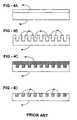
- FIGS. 3A through 3Dare cross-sectional side views illustrating steps in the process of forming conductive rails by a subtractive method.
- FIGS. 4A through 4Dare cross-sectional side views illustrating steps in the process of forming conductive rails by a Damascene method.
- FIG. 5is a cross-sectional side view of the device layers prior to the formation of the pillar structures.
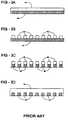
- FIGS. 6 through 10are cross-sectional side views ( Figures with subpart A and C) and top views ( Figures with subpart B) of process steps of making a device array according to one embodiment of the invention.
- FIGS. 11A through 11Fare cross-sectional side views of process steps of making a wiring structure according to another alternative embodiment of the invention.
- FIGS. 12A through 12Bare cross-sectional side views of process steps of making a wiring structure according to another alternative embodiment of the invention.
- the present inventorsrealized that instead of using sidewall spacers as mask for etching device layers, the sidewall spacers may instead be used as sacrificial spacers when forming the etching mask. Once the etching mask is formed, the sidewall spacers are removed and portions of the device layers located below the former sidewall spacer locations are removed to leave spaced apart devices, such as pillar shaped devices.
- At least two spaced apart featuresare then formed over the device layers.
- a plurality (i.e., more than two) featuresare formed to form a large device array.
- the featuresmay be formed directly on or above semiconductor, conductive and/or insulating device layers.
- the featuresmay have any shape and may be made of any material as long as these features can subsequently function as an etching mask for etching the underlying device layers.
- Sidewall spacersare then formed on the features.
- Sidewall spacersmay be formed by conventional sidewall spacer formation methods, such as by depositing a film over the features and then anisotropically etching the film to leave sidewall spacers on the features.
- the spacersmay be made of a conductive, insulating or semiconductor material different from that of the upper portions of the features.
- the sidewall spacer materialcan be selected i) such that it can be selectively anisotropically etched with dry etch chemistry compared to the material in at least the upper portions of the features; and ii) such that it can be selectively removed (such as isotropically etched) compared to the material in at least the upper portions of the features using a different dry or wet etch chemistry.
- the spacersmay be formed from silicon oxide.
- the spacersmay be formed from a nitride, such as silicon nitride. Other material combinations may also be used.
- the original featuresare selectively removed.
- the removalmay be performed by selective wet etching for example.
- the step of selectively removingcomprises selectively etching the material of the original features without substantially removing the sidewall spacer material.
- the removal of the original featuresleaves the sidewall spacers spaced apart from one another.
- the filler featuresmay be formed by forming a filler film or layer over and between the sidewall spacers, followed by planarizing the filler film to expose upper portions of the sidewall spacers.
- the planarizationcan be carried out by chemical-mechanical polishing (CMP) or etchback.
- CMPchemical-mechanical polishing
- the CMP processcan use the upper portions of the spacers as a polish stop.
- a TiN hard mask on the featuresmay be used as a polish stop.
- the filler filmmay comprise the same or different material as the features.
- the filler film materialshould be different from the material of the sidewall spacers so that the sidewall spacers can be selectively etched compared to the filler features.
- the filler film materialmay comprise tungsten, amorphous carbon, silicon nitride or silicon oxynitride.
- the filler film materialmay comprise silicon oxide when the spacers are made of material other than silicon oxide.
- the sidewall spacersare selectively removed.
- the removalmay be performed by selective wet etching for example.
- the step of selectively removingcomprises selectively etching the material of the sidewall spacers without substantially removing the filler feature material. The removal of the spacers leaves the filler features spaced apart from each other.
- the spaced apart filler featuresthen function as etching mask during the etching of the underlying device layers.
- the device layersmay be etched using isotropic or anisotropic etching using the filler features as a mask.
- the filler featuresmay be retained in a completed device or removed after etching the device layers.
- the conductive filler featuresmay be retained as portions of upper electrodes.
- the devicesmay have a substantially cylindrical and/or substantially rectangular pillar shape, depending on the shape of the features and the filler features, as will be described in more detail below.
- Non-pillar shaped devicesmay also be formed.
- the devicesmay comprise diodes, transistors, resistors, antifuse dielectrics, fuses, resistivity-switching materials, capacitors, etc.
- Logic, volatile memory or nonvolatile memory devices or arraysmay be formed.
- the pillar structures described in U.S. application Ser. No. 12/000,758 filed on Dec. 17, 2007 to Petti et. al., which is hereby incorporated by reference in its entirety,may be formed.
- a plurality of pillar shaped devicesthat comprise a plurality of diodes containing nonvolatile memory cells are formed.
- U.S. Pat. No. 6,952,030issued to Herner et al. and entitled “High-Density Three-Dimensional Memory Cell,” hereinafter the “'030 patent” and hereby incorporated by reference in its entirety, discloses an exemplary nonvolatile memory cell which can be formed by the method of the embodiments of the present invention.
- the memory cell 20includes a vertically oriented, cylindrical pillar shaped junction diode.
- junction diodeis used herein to refer to a semiconductor device with the property of non-ohmic conduction, having two terminal electrodes, and made of semiconducting material which is p-type at one electrode and n-type at the other. Examples include p-n diodes and n-p diodes, which have a p-type semiconductor material and an n-type semiconductor material in contact, such as Zener diodes, and p-i-n diodes, in which an intrinsic (undoped) semiconductor material is interposed between the p-type semiconductor material and the n-type semiconductor material.
- the diode 22 and an optional antifuse dielectric 24are interposed between top 26 and bottom 28 conductors or electrodes.
- the vertically oriented junction diode 22includes a heavily doped semiconductor region 30 of a first conductivity type (such as n-type), an intermediate region 32 which is undoped semiconductor material or lightly doped semiconductor material (which will be referred to as an intrinsic region), and a heavily doped semiconductor region 34 of the second conductivity type (such as p-type) to form a p-i-n diode. If desired, the location of the p and n-type regions may be reversed.
- the semiconductor material of the junction diode 22is generally silicon, germanium, or an alloy of silicon and/or germanium. Other semiconductor materials may also be used.
- junction diode 22 and the antifuse dielectric 24are arranged in series between the bottom conductor 28 and the top conductor 26 , which may be formed of a metal or any other conductor, such as tungsten and/or TiN.
- the antifuse dielectric 24may be located above or below the diode 22 .
- the memory cellmay comprise a one-time programmable (OTP) or re-writable nonvolatile memory cell.
- OTPone-time programmable
- each diode 22may act as a steering element of a memory cell and another material or layer 24 which acts as a resistivity switching material (i.e., which stores the data) is provided in series with the diode between the conductors.
- the resistivity switching material 24may comprise a fuse, polysilicon memory effect material, metal oxide (such as nickel oxide, perovskite materials, etc,), carbon nanotubes, phase change materials, switchable complex metal oxides, conductive bridge elements, or switchable polymers.
- the resistivity of the resistivity switching material 24may be increased or decreased in response to a forward and/or reverse bias provided between the electrodes or conductors.
- the cell 20operates as follows. In the initial state, very little current flows through the junction diode 22 when a read voltage is applied between the top conductor 26 and the bottom conductor 28 because the antifuse dielectric 24 impedes current flow. The application of a programming voltage between the top conductor 26 and bottom conductor 28 causes dielectric breakdown of the antifuse material, permanently forming a conductive path through the antifuse 24 . If the diode semiconductor material is initially formed in a high resistivity state, then the semiconductor material of diode 22 may be altered as well, changing it to a lower-resistivity state. After programming, a higher read current flows between the top conductor 26 and the bottom conductor 28 upon application of a read voltage. In this way, a programmed cell can be distinguished from an unprogrammed cell.
- the antifuse dielectric 24may be omitted.
- the polycrystalline semiconductor material of diode 22is formed in a relatively high-resistivity state, which also tends to impede current flow, as described in a U.S. patent application Ser. No. 10/955,549, “Nonvolatile Memory Cell Without a Dielectric Antifuse Having High- and Low-Impedance States,” filed by Herner et al. on Sep. 29, 2004 and hereinafter the “'549 application”; and U.S. patent application Ser. No. 11/148,530, “Nonvolatile Memory Cell Operating by Increasing Order in Polycrystalline Semiconductor Material,” filed by Herner et al. on Jun. 8, 2005 and hereinafter the “ '530 application,” both hereby incorporated by reference.
- the application of a programming voltagelowers the resistivity state of the diode.
- the diodeacts as a resistivity switching material in this embodiment.
- a portion of a first memory level 36 of memory cells 20 similar to the cell 20 of FIG. 1is shown.
- Two, three, four, or more such memory levels, such as eight levelsmay be formed, stacked one atop the other, to form a monolithic three dimensional memory array, preferably formed above a substrate such as a monocrystalline silicon wafer, and described in the '030 patent and the '549 and '530 applications.
- the diode pillars 22preferably have a pitch of less than 100 nm, such as pitch of 78 nm or less and a diameter of 100 nm or less, such as 50 nm or less, such as 32 nm for example.
- the bottom electrodes or conductors 28can be formed either by subtractive or by Damascene methods.
- a subtractive methoda conductive layer or film is patterned into spaced apart electrodes and the gaps between the electrodes are then filled with an insulating material.
- a Damascene methodgrooves are formed in an insulating material, a conductive layer or film is formed in the grooves and over the insulating layer, and then the conductive layer or film is planarized to leave spaced apart electrodes in the grooves.
- FIGS. 3A-3Dillustrate the subtractive method of forming rail-shaped electrodes or conductors 28 .
- one or more conductive layers 40such as a W and/or a TiN layers are deposited over a substrate, and a layer of photoresist 42 is spun onto it.
- the layer of photoresist 42is then photolithographically patterned into the desired form.
- an etch stepremoves portions of the conductive layer(s) 40 where they are not protected by etched photoresist layer 42 .
- the photoresist layer 42is stripped, leaving conductor or electrode rails 40 behind.
- the gaps between the rails 40are filled with an insulating material 44 , such as silicon oxide, silicon nitride or other insulating materials. If desired, any overfill of the insulating material 44 can be removed, for example by chemical-mechanical polishing (CMP), to expose the upper surface of the rails 40 in the planarized surface of the insulating layer 44 .
- CMPchemical-mechanical polishing
- FIGS. 4A to 4Dillustrate an example of the Damascene method to form the electrode or conductor 28 .
- a layer of photoresist 48is spun onto a deposited insulating layer 50 , such as a silicon oxide layer.
- the layer of photoresist 48is patterned.
- An etch stepthen forms grooves or trenches 52 in the insulating layer 50 .
- one or more conductive layers 46such as a W and/or TiN layers are deposited to fill the grooves or trenches 52 .
- the one or more conductive layers 46are planarized, for example by CMP or etchback, with the upper surface of the insulating layer to leave the rail shaped conductors in the grooves, as shown in FIG. 4D .
- FIG. 5shows an initial stage of fabrication of a semiconductor device, such as a pillar shaped nonvolatile memory cell array 110 , according to one embodiment of the invention.
- the array 110contains a plurality of bottom electrodes 114 formed by the subtractive or Damascene methods described above with respect to FIGS. 3 or 4 respectively.
- the electrodes 114correspond to the rail shaped conductors 28 shown in FIGS. 1 and 2 .
- the electrodes 114may comprise any suitable conductive material, such as tungsten, aluminum, their alloys, etc.
- the electrodes 114are separated from each other by an insulating material 116 , such as silicon oxide.
- An optional adhesion layer 118is formed above the electrodes 114 .
- the adhesion layermay comprise titanium nitride or tungsten nitride.
- the optional antifuse dielectric layer 120is deposited over the adhesion layer 118 .
- the antifuse dielectric layer 120may comprise a thin silicon oxide or other insulating layer, such as a high dielectric constant insulating layer. Alternatively, another resistivity switching material described above may be substituted from the antifuse dielectric layer.
- Another optional adhesion layer 122such a TiN layer, is deposited over the antifuse dielectric layer 120 . Therefore, the dielectric layer 120 is sandwiched between two adhesion layers 118 , 122 .
- An optional upper adhesion layer 126is formed over the semiconductor layers 124 .
- Layer 126may have a thickness of between about 100 ⁇ and about 300 ⁇ , such as between about 150 ⁇ and about 200 ⁇ .
- a hard mask layer 128such as a W or amorphous carbon layer, is formed over the adhesion layer 126 .
- Layer 128may be a lower antireflective layer (such as a DARC layer) that is between about 250 ⁇ and about 750 ⁇ thick, such as between about 400 ⁇ and about 500 ⁇ thick.
- an upper layer 130such as a TiN, silicon nitride, or silicon oxynitride layer is formed on the hard mask layer 128 .
- FIG. 6Arepresents a side cross-sectional view of the device layers and FIG. 6B represents a top view of the same after the first step.
- a photoresist layeris formed on the layer 130 .
- an upper antireflective layersuch as a BARC layer, may be formed between the photoresist and layer 130 .
- the critical diameter (“CD”)is between about 50 to about 60 nm, with a diagonal pitch of about 90 nm.
- the photoresist layeris exposed and patterned.
- the photoresist patternis then used as a mask to etch layers 128 and 130 into a plurality of features 132 .
- the featuresare spaced apart from each other by spaces 134 (in the horizontal and vertical directions as shown in FIG. 6B ).
- layer 130may then be removed, resulting in a CD of about 32 nm.
- the features 132are preferably arranged along a plurality of imaginary diagonal lines 136 in a rhombus or rotated square type pattern, as shown in FIG. 6B . Only four of the plurality of diagonal lines 136 are shown in FIG. 6B for clarity. As shown in FIG. 6B , the features 132 preferably have a substantially cylindrical shape (i.e., they have a circular or near circular (such as oval) cross section).
- Alignment edge features 137are provided adjacent to the device array boundary, as shown in FIG. 6B .
- the alignment edge featuresmay have a larger size than the plurality of spaced apart features 132 and/or they may have a different shape, such as an oval cross sectional shape.
- the alignment edge featureswill be used to simplify alignment in the cut mask step that will be described below.
- FIGS. 7A and 7Bshow the next process step.
- silicon oxide or silicon nitride spacers 138are formed on each feature 132 .
- each feature 132is cylindrical, then it technically has only one sidewall and only one ring or annulus shaped spacer 138 is formed around the sidewall of the feature 132 .
- the term “spacers”will denote the single annular spacer 138 as well as two or more spacers 138 formed on discrete sidewalls of a polygonal feature 132 .
- the spacers 138are formed by depositing a silicon oxide or nitride layer or film over and between the features 132 followed by anisotropic etching of the silicon oxide or nitride layer or film.
- the spacers 138fill the spaces 134 around the features 132 primarily along the plurality of diagonal lines 136 , leaving discrete spaces or interstices 140 between adjacent sidewall spacers 138 . Due to the annular shape of the sidewall spacers 138 , the interstices have a rectangular cross sectional shape with concave sidewalls, as shown in FIG. 7 b .
- the original features 132are then removed by selective etching, leaving the spacers 138 spaced apart from one another, as shown in FIG. 7C . If the features 132 are made of amorphous carbon, then ashing can be used to remove them.
- FIGS. 8A and 8Bshow the next two steps of the process.
- a tungsten filler material film or layeris formed between the spacers 138 , filling the space initially occupied by the original features 132 and the spaces 134 .
- an insulating filler material film or layersuch as silicon oxide, silicon nitride, silicon oxynitride, amorphous carbon, which has different etch characteristics from the spacer material may be used instead.
- the tungsten filler filmis then planarized by CMP or etchback to expose the upper surfaces of the spacers 138 , resulting in a loss of about 200 to about 400 ⁇ , such as about 300 ⁇ to about 500 ⁇ , of the tungsten filler film.
- the planarizationleaves a plurality of tungsten filler features 142 between the spacers 138 .
- the features 142 at this point of the processmay be between about 1500 ⁇ and about 1700 ⁇ thick. Since some of the filler features 142 B fill the interstices 140 , these filler features 142 B have a rectangular or square cross sectional shape with concave sidewalls (i.e., a substantially rectangular or square shape). If the original features 132 have a cylindrical shape, then the filler features 142 A that fill the spaces previously occupied by features 132 also have a cylindrical shape, as shown in FIG. 8B . At this point in the fabrication of the device array, the spaces 134 are completely filled with either spacers 138 or filler features 142 .
- an optional cut masking and etching stepis performed after the planarization of the filler film to remove the filler film or filler features 142 from the area outside of the device array.
- a photoresist layeris formed over the plurality of filler features 142 .
- the photoresist layeris exposed such that the edges of the exposed areas intersect all of the edge features 137 . Elongating or enlarging the edge features 137 thus allows for an easier alignment of this cut mask.
- the remaining filler film or filler features remaining in areas outside of the device array boundary that are not covered by the photoresist patternare etched away. If desired, the cut masking and etching step can be performed prior to the planarization step.
- FIGS. 9A and 9Bshow the next step in the process.
- the spacers 138are selectively etched away leaving the filler features 142 spaced apart by spaces 145 .
- the spacers 138may be selectively etched by any selective wet or dry etch which can selectively etch silicon oxide or nitride of spaces 138 over the tungsten material of filler features 142 .
- an HF isotropic wet etchmay be used.
- the device layers 118 , 120 , 122 and 124are etched using the filler features 142 as a mask to form a plurality of pillar shaped devices 112 .
- each of the devicescomprises the p-i-n diode in series with an antifuse dielectric, as described with respect to FIG. 1 .
- the pillar shaped devices 112have a pitch which is double that of what the pitch would have been had only the features 132 been used as mask.
- the spaces between the pillar devices 112are filled with a gap fill insulating material, such as silicon oxide, to isolate the devices 112 from each other.
- the gap fill insulating materialmay be planarized by CMP or etchback.
- the filler features 142may be either retained in the final device or removed after the formation of the pillar devices 112 .
- the filler features 142may be retained in contact with the upper part of the devices 112 .
- the upper conductors or electrodes 26 shown in FIG. 1are then formed in contact with the filler features 142 .
- 400-500 ⁇ of tungsten filler features 142may remain in the device shown in FIGS. 10A-10B .
- the filler features 142may be removed prior to formation of the upper conductors or electrodes 26 .
- the upper conductors or electrodes 26may be formed by the subtractive or the Damascene processes described above with respect to FIGS. 3 or 4 .
- FIGS. 11A-11Fillustrate the process steps of making a wiring structure according to an alternative embodiment of the invention.
- the method of this embodimentcan be used together with the method of the prior embodiment to form the lower wiring for the semiconductor pillar devices.
- the methodcan be used to form wiring for other non-pillar shaped devices or for pillar devices made by other methods.
- FIG. 11Aillustrates a first step in the method in which a photoresist pattern 201 of about 500 to about 2000 ⁇ thick, or preferably about 1200 ⁇ thick is formed on one or more antireflective and/or hard mask layers.
- the photoresist patternmay be formed by exposing a photoresist layer to any suitable radiation, such as 193 nm radiation and developing the photoresist layer.
- the CD of the photoresist patternis about 54 to about 64 nm, with a pitch of about 128 nm.
- the photoresist patternmay be formed on an upper antireflective layer, such as a BARC layer 202 , which can be about 200 to about 400 ⁇ , such as 250 ⁇ , in thickness.
- a layer of insulating materialsuch as a silicon oxynitride DARC layer 203 , which is about 300 to about 500 ⁇ , such as about 400 ⁇ , thick, may be located below this BARC layer.
- a layer of hard mask materialsuch as an amorphous carbon advanced patterning film (APF) 204 A, may be located below the insulating layer 203 .
- the thickness of the hard mask layermay be about 1000 to 3000 ⁇ , such as about 2000 ⁇ .
- the hard mask (amorphous carbon)may be located above an insulating layer 205 , such as a silicon oxide or other insulating layer.
- Layer 205may have a thickness of about 2000 to about 4000 ⁇ , such as 3000 ⁇ .
- the insulating layer 205may be located over a semiconductor wafer or other suitable substrate. Various circuits or devices may be located on or in the substrate. Any one of the BARC 202 , DARC 203 , and APF 204 A are optional and can be omitted.
- FIG. 11Bshows the next process step, in which the BARC layer, the DARC layer, and the hard mask layer are etched using the resist pattern 201 as a mask.
- the photoresist, DARC layer, and BARC layerare then selectively removed to leave hard mask structures 204 B, with a CD of about 32 nm. Other CD may also be used.
- the hard mask structures 204 Bbecome masking features, similar to the feature 132 described with respect to FIGS. 6 to 10 . Any hard mask material other than amorphous carbon may be used to form structures 204 B.
- sidewall spacers 206are formed on each hard mask structure 204 B.
- Any spacer materialsuch as silicon nitride, silicon oxide, silicon oxynitride, may be used. It should be noted that if each structure is cylindrical, then it technically has only one sidewall and only one ring or annulus shaped spacer is formed around the sidewall of the structure. If the structures 204 B are rail shaped, then two spacers 206 are formed on opposite sidewalls of the structures 204 B. The spacers are formed by depositing a silicon oxide or nitride layer or film over and between the structures followed by anisotropic etching of the silicon nitride or oxide layer or film.
- the hard mask structures 204 Bare then removed by selective etching or ashing, leaving the spacers 206 spaced apart from one another, as shown in FIG. 11D .
- ashingis employed to remove them.
- FIGS. 11E and 11Fillustrate the next two steps of the process.
- the spacers 206act as a mask, and the oxide insulating layer 205 below the spacers is etched to form line structures 209 and grooves and/or trenches 207 between the insulating line 209 .
- the spacers 206are then selectively etched away by any selective wet or dry etch.
- An electrically conductive filler materialis then deposited to form a film or layer over and between the oxide line structures.
- the filler materialmay comprise one or more conductive layers, such as tungsten, copper, aluminum, tantalum, titanium, titanium nitride, etc.
- the conductive filler filmis then planarized by CMP or etchback to expose the upper surfaces of the oxide line structures 209 .
- the resulting thickness of the conductive filler features 208 in the trenchesis about the same as the depth of the trenches 207 created by the previous etching, which is about 1000 to about 3000 ⁇ , such as 2000 ⁇ .
- the CMP processleaves a structure with insulating line structures 209 electrically isolating separating adjacent conductive filler features 208 , which can function as electrodes for a semiconductor or other solid state device.
- the electrodes 208may be rail shaped and may be located below the semiconductor devices described in the prior embodiment. Thus, the conductive electrodes 208 are formed in the trenches 207 by a damascene process.
- FIGS. 12A and 12BAnother alternative embodiment to form conductive electrodes is illustrated in FIGS. 12A and 12B .
- the insulating layer 205is not etched to form trenches 207 as shown in FIG. 11E .
- the hard mask pillars 204 Bare removed as shown in FIGS. 11D and 12A , leaving spacers 206 spaced apart from one another.
- the conductive filler material described in the prior embodimentis deposited to form a film or layer over and between the spacers 206 .
- the conductive filmis then planarized by CMP or etchback to form electrodes 208 by a damascene process.
- Each electrode 208is separated and electrically isolated from adjacent electrodes 208 by an insulating spacer 206 .
- the height of the electrodes 208is comparable to the height of the spacers 206 , which is between about 1000 to about 3000 ⁇ , such as 2000 ⁇ .
- Formation of a first memory levelhas been described. Additional memory levels can be formed above this first memory level to form a monolithic three dimensional memory array.
- conductorscan be shared between memory levels; i.e. top conductor would serve as the bottom conductor of the next memory level.
- an interlevel dielectric(not shown) is formed above the first memory level, its surface planarized, and construction of a second memory level begins on this planarized interlevel dielectric, with no shared conductors.
- a monolithic three dimensional memory arrayis one in which multiple memory levels are formed above a single substrate, such as a wafer, with no intervening substrates.
- the layers forming one memory levelare deposited or grown directly over the layers of an existing level or levels.
- stacked memorieshave been constructed by forming memory levels on separate substrates and adhering the memory levels atop each other, as in Leedy, U.S. Pat. No. 5,915,167, “Three dimensional structure memory.”
- the substratesmay be thinned or removed from the memory levels before bonding, but as the memory levels are initially formed over separate substrates, such memories are not true monolithic three dimensional memory arrays.
- a monolithic three dimensional memory array formed above a substratecomprises at least a first memory level formed at a first height above the substrate and a second memory level formed at a second height different from the first height. Three, four, eight, or indeed any number of memory levels can be formed above the substrate in such a multilevel array.
Landscapes
- Engineering & Computer Science (AREA)
- Physics & Mathematics (AREA)
- Condensed Matter Physics & Semiconductors (AREA)
- General Physics & Mathematics (AREA)
- Manufacturing & Machinery (AREA)
- Computer Hardware Design (AREA)
- Microelectronics & Electronic Packaging (AREA)
- Power Engineering (AREA)
- Chemical & Material Sciences (AREA)
- Inorganic Chemistry (AREA)
- Semiconductor Memories (AREA)
- Internal Circuitry In Semiconductor Integrated Circuit Devices (AREA)
Abstract
Description
Claims (16)
Priority Applications (3)
| Application Number | Priority Date | Filing Date | Title |
|---|---|---|---|
| US12/149,151US7786015B2 (en) | 2008-04-28 | 2008-04-28 | Method for fabricating self-aligned complementary pillar structures and wiring |
| PCT/US2009/002400WO2009134323A1 (en) | 2008-04-28 | 2009-04-17 | Method for fabricating self-aligned complimentary pillar structures and wiring |
| TW098113921ATW201005873A (en) | 2008-04-28 | 2009-04-27 | Method for fabricating self-aligned complimentary pillar structures and wiring |
Applications Claiming Priority (1)
| Application Number | Priority Date | Filing Date | Title |
|---|---|---|---|
| US12/149,151US7786015B2 (en) | 2008-04-28 | 2008-04-28 | Method for fabricating self-aligned complementary pillar structures and wiring |
Publications (2)
| Publication Number | Publication Date |
|---|---|
| US20090269932A1 US20090269932A1 (en) | 2009-10-29 |
| US7786015B2true US7786015B2 (en) | 2010-08-31 |
Family
ID=40983455
Family Applications (1)
| Application Number | Title | Priority Date | Filing Date |
|---|---|---|---|
| US12/149,151ActiveUS7786015B2 (en) | 2008-04-28 | 2008-04-28 | Method for fabricating self-aligned complementary pillar structures and wiring |
Country Status (3)
| Country | Link |
|---|---|
| US (1) | US7786015B2 (en) |
| TW (1) | TW201005873A (en) |
| WO (1) | WO2009134323A1 (en) |
Cited By (15)
| Publication number | Priority date | Publication date | Assignee | Title |
|---|---|---|---|---|
| US20100112483A1 (en)* | 2008-10-30 | 2010-05-06 | Wing Ngai Christopher Siu | System and method for self-aligned dual patterning |
| US20100167520A1 (en)* | 2008-12-31 | 2010-07-01 | Sandisk 3D Llc | Resist feature and removable spacer pitch doubling patterning method for pillar structures |
| US20100184259A1 (en)* | 2007-06-27 | 2010-07-22 | Radigan Steven J | Method for fabricating a 3-d integrated circuit using a hard mask of silicon-oxynitride on amorphous carbon |
| US20100193916A1 (en)* | 2008-12-31 | 2010-08-05 | Sandisk 3D Llc | Methods for increased array feature density |
| US8080443B2 (en) | 2008-10-27 | 2011-12-20 | Sandisk 3D Llc | Method of making pillars using photoresist spacer mask |
| US20130034963A1 (en)* | 2011-08-02 | 2013-02-07 | Chung Byung-Hong | Methods of forming fine patterns for semiconductor device |
| US20130137270A1 (en)* | 2011-11-24 | 2013-05-30 | Powerchip Technology Corporation | Method for forming contact hole |
| US8889558B2 (en) | 2012-12-12 | 2014-11-18 | Micron Technology, Inc. | Methods of forming a pattern on a substrate |
| US8889559B2 (en) | 2012-12-12 | 2014-11-18 | Micron Technology, Inc. | Methods of forming a pattern on a substrate |
| US8937018B2 (en) | 2013-03-06 | 2015-01-20 | Micron Technology, Inc. | Methods of forming a pattern on a substrate |
| US8999852B2 (en) | 2012-12-12 | 2015-04-07 | Micron Technology, Inc. | Substrate mask patterns, methods of forming a structure on a substrate, methods of forming a square lattice pattern from an oblique lattice pattern, and methods of forming a pattern on a substrate |
| US9018048B2 (en) | 2012-09-27 | 2015-04-28 | Stmicroelectronics S.R.L. | Process for manufactuirng super-barrier rectifiers |
| US9184058B2 (en) | 2013-12-23 | 2015-11-10 | Micron Technology, Inc. | Methods of forming patterns by using a brush layer and masks |
| US10847376B2 (en) | 2018-06-28 | 2020-11-24 | Sandisk Technologies Llc | In-situ deposition and etch process and apparatus for precision patterning of semiconductor devices |
| US10957648B2 (en) | 2018-07-20 | 2021-03-23 | Sandisk Technologies Llc | Three-dimensional memory device containing contact via structure extending through source contact layer and dielectric spacer assembly |
Families Citing this family (20)
| Publication number | Priority date | Publication date | Assignee | Title |
|---|---|---|---|---|
| US7732235B2 (en)* | 2008-06-30 | 2010-06-08 | Sandisk 3D Llc | Method for fabricating high density pillar structures by double patterning using positive photoresist |
| KR20100083581A (en)* | 2009-01-14 | 2010-07-22 | 삼성전자주식회사 | Methods of forming semiconductor device |
| US7902869B1 (en) | 2010-04-30 | 2011-03-08 | Hewlett-Packard Development Company, L.P. | Extensible three dimensional circuit |
| US9818478B2 (en) | 2012-12-07 | 2017-11-14 | Attopsemi Technology Co., Ltd | Programmable resistive device and memory using diode as selector |
| US9711237B2 (en) | 2010-08-20 | 2017-07-18 | Attopsemi Technology Co., Ltd. | Method and structure for reliable electrical fuse programming |
| US10229746B2 (en) | 2010-08-20 | 2019-03-12 | Attopsemi Technology Co., Ltd | OTP memory with high data security |
| US10916317B2 (en) | 2010-08-20 | 2021-02-09 | Attopsemi Technology Co., Ltd | Programmable resistance memory on thin film transistor technology |
| US10923204B2 (en) | 2010-08-20 | 2021-02-16 | Attopsemi Technology Co., Ltd | Fully testible OTP memory |
| US10249379B2 (en) | 2010-08-20 | 2019-04-02 | Attopsemi Technology Co., Ltd | One-time programmable devices having program selector for electrical fuses with extended area |
| US10192615B2 (en) | 2011-02-14 | 2019-01-29 | Attopsemi Technology Co., Ltd | One-time programmable devices having a semiconductor fin structure with a divided active region |
| US10586832B2 (en) | 2011-02-14 | 2020-03-10 | Attopsemi Technology Co., Ltd | One-time programmable devices using gate-all-around structures |
| KR20130043533A (en)* | 2011-10-20 | 2013-04-30 | 삼성전자주식회사 | Non-volatile memory device having conductive buffer pattern and method of forming the same |
| CN103187243B (en)* | 2011-12-31 | 2016-03-02 | 中芯国际集成电路制造(北京)有限公司 | The manufacture method of semiconductor device |
| CN103779263B (en)* | 2012-10-18 | 2017-03-08 | 中芯国际集成电路制造(上海)有限公司 | A kind of manufacture method of the semiconductor device based on self-aligned double patterning case |
| US10535413B2 (en) | 2017-04-14 | 2020-01-14 | Attopsemi Technology Co., Ltd | Low power read operation for programmable resistive memories |
| US11062786B2 (en) | 2017-04-14 | 2021-07-13 | Attopsemi Technology Co., Ltd | One-time programmable memories with low power read operation and novel sensing scheme |
| US10726914B2 (en) | 2017-04-14 | 2020-07-28 | Attopsemi Technology Co. Ltd | Programmable resistive memories with low power read operation and novel sensing scheme |
| US11615859B2 (en) | 2017-04-14 | 2023-03-28 | Attopsemi Technology Co., Ltd | One-time programmable memories with ultra-low power read operation and novel sensing scheme |
| US10770160B2 (en) | 2017-11-30 | 2020-09-08 | Attopsemi Technology Co., Ltd | Programmable resistive memory formed by bit slices from a standard cell library |
| US10930705B2 (en)* | 2018-03-28 | 2021-02-23 | International Business Machines Corporation | Crystallized silicon vertical diode on BEOL for access device for confined PCM arrays |
Citations (84)
| Publication number | Priority date | Publication date | Assignee | Title |
|---|---|---|---|---|
| GB1476585A (en) | 1974-06-28 | 1977-06-16 | Rca Corp | Method for manufacturing semiconductor devices |
| US4151602A (en) | 1975-04-02 | 1979-04-24 | U.S. Philips Corporation | Magnetic bubble multilayer arrangement |
| US4201800A (en) | 1978-04-28 | 1980-05-06 | International Business Machines Corp. | Hardened photoresist master image mask process |
| US4646266A (en) | 1984-09-28 | 1987-02-24 | Energy Conversion Devices, Inc. | Programmable semiconductor structures and methods for using the same |
| EP0288739A2 (en) | 1987-04-30 | 1988-11-02 | International Business Machines Corporation | Method of self-aligning a trench isolation structure to an implanted well region |
| US5024971A (en) | 1990-08-20 | 1991-06-18 | Motorola, Inc. | Method for patterning submicron openings using an image reversal layer of material |
| US5482885A (en)* | 1994-03-18 | 1996-01-09 | United Microelectronics Corp. | Method for forming most capacitor using poly spacer technique |
| US5667940A (en) | 1994-05-11 | 1997-09-16 | United Microelectronics Corporation | Process for creating high density integrated circuits utilizing double coating photoresist mask |
| US5739068A (en) | 1995-02-22 | 1998-04-14 | Micron Technology, Inc. | Semiconductor processing method of making electrical contact to a node received within a mass of insulating dielectric material |
| US5751012A (en) | 1995-06-07 | 1998-05-12 | Micron Technology, Inc. | Polysilicon pillar diode for use in a non-volatile memory cell |
| US5835396A (en) | 1996-10-17 | 1998-11-10 | Zhang; Guobiao | Three-dimensional read-only memory |
| US5915167A (en) | 1997-04-04 | 1999-06-22 | Elm Technology Corporation | Three dimensional structure memory |
| US5977638A (en) | 1996-11-21 | 1999-11-02 | Cypress Semiconductor Corp. | Edge metal for interconnect layers |
| US5998287A (en) | 1994-06-13 | 1999-12-07 | United Microelectronics Corp. | Process for producing very narrow buried bit lines for non-volatile memory devices |
| US6034882A (en) | 1998-11-16 | 2000-03-07 | Matrix Semiconductor, Inc. | Vertically stacked field programmable nonvolatile memory and method of fabrication |
| US6055180A (en) | 1997-06-17 | 2000-04-25 | Thin Film Electronics Asa | Electrically addressable passive device, method for electrical addressing of the same and uses of the device and the method |
| US6096659A (en) | 1998-04-13 | 2000-08-01 | Advanced Micro Devices, Inc. | Manufacturing process for reducing feature dimensions in a semiconductor |
| US6140234A (en) | 1998-01-20 | 2000-10-31 | International Business Machines Corporation | Method to selectively fill recesses with conductive metal |
| US6221562B1 (en) | 1998-11-13 | 2001-04-24 | International Business Machines Corporation | Resist image reversal by means of spun-on-glass |
| US20020052068A1 (en) | 1997-11-25 | 2002-05-02 | Werner Juengling | Dram capacitor array and integrated device array of substantially identically shaped devices |
| US20020072208A1 (en) | 1999-09-02 | 2002-06-13 | Fernando Gonzalez | Methods of forming dram assemblies, transistor devices, and openings in substrates |
| US6420215B1 (en) | 2000-04-28 | 2002-07-16 | Matrix Semiconductor, Inc. | Three-dimensional memory array and method of fabrication |
| US6420231B1 (en) | 1999-06-30 | 2002-07-16 | Sandisk Corporation | Processing techniques for making a dual floating gate EEPROM cell array |
| US20020172901A1 (en) | 1998-11-09 | 2002-11-21 | Nec Corporation | Method of exposing a lattice pattern onto a photo-resist film |
| US6492075B1 (en) | 2000-06-16 | 2002-12-10 | Advanced Micro Devices, Inc. | Chemical trim process |
| US6496401B2 (en) | 2000-05-31 | 2002-12-17 | Infineon Technologies Ag | Memory cell configuration |
| US20030122156A1 (en) | 2001-06-26 | 2003-07-03 | Jon Maimon | Programmable resistance memory element and method for making same |
| US20030157436A1 (en) | 2002-02-20 | 2003-08-21 | Dirk Manger | Method for forming a hard mask in a layer on a planar device |
| US6618295B2 (en) | 2001-03-21 | 2003-09-09 | Matrix Semiconductor, Inc. | Method and apparatus for biasing selected and unselected array lines when writing a memory array |
| US20030178684A1 (en) | 1996-11-06 | 2003-09-25 | Fujitsu Limited | Semiconductor device and method for fabricating the same |
| US6631085B2 (en) | 2000-04-28 | 2003-10-07 | Matrix Semiconductor, Inc. | Three-dimensional memory array incorporating serial chain diode stack |
| WO2004061851A2 (en) | 2002-12-19 | 2004-07-22 | Matrix Semiconductor, Inc | An improved method for making high-density nonvolatile memory |
| US20040241993A1 (en) | 2003-05-29 | 2004-12-02 | Chun-Jung Lin | Method for forming double density wordline |
| US20040245557A1 (en) | 2003-06-03 | 2004-12-09 | Samsung Electronics Co., Ltd. | Nonvolatile memory device comprising one switching device and one resistant material and method of manufacturing the same |
| US20050014385A1 (en) | 2003-07-15 | 2005-01-20 | Ghozeil Adam L. | Array of nanoscopic mosfet transistors and fabrication methods |
| US6856572B2 (en) | 2000-04-28 | 2005-02-15 | Matrix Semiconductor, Inc. | Multi-headed decoder structure utilizing memory array line driver with dual purpose driver device |
| US6855614B2 (en)* | 2000-11-13 | 2005-02-15 | Integrated Discrete Devices, Llc | Sidewalls as semiconductor etch stop and diffusion barrier |
| US20050052915A1 (en) | 2002-12-19 | 2005-03-10 | Matrix Semiconductor, Inc. | Nonvolatile memory cell without a dielectric antifuse having high- and low-impedance states |
| US6879505B2 (en) | 2003-03-31 | 2005-04-12 | Matrix Semiconductor, Inc. | Word line arrangement having multi-layer word line segments for three-dimensional memory array |
| US20050112812A1 (en) | 2003-11-20 | 2005-05-26 | Wen-Yueh Jang | Method for forming narrow trench structures |
| US20050170294A1 (en) | 2003-10-15 | 2005-08-04 | Yuji Kobayashi | Method of forming contact hole and method of manufacturing semiconductor device |
| US20050196684A1 (en) | 2004-02-23 | 2005-09-08 | Hiroko Nakamura | Mask pattern data producing method, patterning method, reticle correcting method, reticle manufacturing method, and semiconductor apparatus manufacturing method |
| US6951780B1 (en) | 2003-12-18 | 2005-10-04 | Matrix Semiconductor, Inc. | Selective oxidation of silicon in diode, TFT, and monolithic three dimensional memory arrays |
| US20050226067A1 (en) | 2002-12-19 | 2005-10-13 | Matrix Semiconductor, Inc. | Nonvolatile memory cell operating by increasing order in polycrystalline semiconductor material |
| US20050269553A1 (en) | 2003-09-08 | 2005-12-08 | Nantero, Inc. | Spin-coatable liquid for use in electronic fabrication processes |
| US20060035167A1 (en) | 2004-08-12 | 2006-02-16 | International Business Machines Corporation | Ultrathin polymeric photoacid generator layer and method of fabricating at least one of a device and a mask by using said layer |
| US20060105476A1 (en) | 2004-01-08 | 2006-05-18 | Yeon-Dong Choi | Photoresist pattern, method of fabricating the same, and method of assuring the quality thereof |
| US20060154182A1 (en) | 2005-01-12 | 2006-07-13 | International Business Machines Corporation | Method for post lithographic critical dimension shrinking using post overcoat planarization |
| US7078348B1 (en) | 2001-06-27 | 2006-07-18 | Advanced Micro Devices, Inc. | Dual layer patterning scheme to make dual damascene |
| US7081377B2 (en) | 2002-06-27 | 2006-07-25 | Sandisk 3D Llc | Three-dimensional memory |
| US20060177977A1 (en) | 2005-02-08 | 2006-08-10 | The Hong Kong University Of Science And Technology | Method for patterning fins and gates in a FinFET device using trimmed hard-mask capped with imaging layer |
| US20060216937A1 (en)* | 2005-03-25 | 2006-09-28 | Matrix Semiconductor, Inc. | Method for reducing dielectric overetch using a dielectric etch stop at a planar surface |
| US20060250837A1 (en) | 2005-05-09 | 2006-11-09 | Sandisk 3D, Llc | Nonvolatile memory cell comprising a diode and a resistance-switching material |
| US20060250836A1 (en) | 2005-05-09 | 2006-11-09 | Matrix Semiconductor, Inc. | Rewriteable memory cell comprising a diode and a resistance-switching material |
| US20060273298A1 (en) | 2005-06-02 | 2006-12-07 | Matrix Semiconductor, Inc. | Rewriteable memory cell comprising a transistor and resistance-switching material in series |
| EP1746645A2 (en) | 2005-07-18 | 2007-01-24 | Saifun Semiconductors Ltd. | Memory array with sub-minimum feature size word line spacing and method of fabrication |
| US7176064B2 (en) | 2003-12-03 | 2007-02-13 | Sandisk 3D Llc | Memory cell comprising a semiconductor junction diode crystallized adjacent to a silicide |
| US20070049035A1 (en) | 2005-08-31 | 2007-03-01 | Tran Luan C | Method of forming pitch multipled contacts |
| US20070059914A1 (en) | 2005-09-14 | 2007-03-15 | Hynix Semiconductor Inc. | Method of forming micro patterns in semiconductor devices |
| US7211866B2 (en) | 2001-08-08 | 2007-05-01 | Sandisk Corporation | Scalable self-aligned dual floating gate memory cell array and methods of forming the array |
| US20070099431A1 (en)* | 2005-11-01 | 2007-05-03 | Micron Technology, Inc. | Process for increasing feature density during the manufacture of a semiconductor device |
| US20070114508A1 (en) | 2005-11-23 | 2007-05-24 | Matrix Semiconductor, Inc. | Reversible resistivity-switching metal oxide or nitride layer with added metal |
| US20070114509A1 (en) | 2005-11-23 | 2007-05-24 | Sandisk 3D Llc | Memory cell comprising nickel-cobalt oxide switching element |
| US20070158688A1 (en) | 2005-09-30 | 2007-07-12 | Dirk Caspary | Memory device and a method of forming a memory device |
| US20070176160A1 (en) | 2006-01-27 | 2007-08-02 | Hamamatsu Photonics K.K. | Electron tube |
| EP1818977A2 (en) | 2006-02-13 | 2007-08-15 | ASML Netherlands B.V. | Lithographic projection apparatus and device manufacturing method |
| US20070197014A1 (en) | 2006-02-17 | 2007-08-23 | Samsung Electronics Co., Ltd. | Method of fabricating semiconductor device |
| WO2007103343A1 (en) | 2006-03-09 | 2007-09-13 | Micron Technology, Inc. | Trim process for critical dimension control for integrated circuits |
| US7271057B2 (en) | 2004-09-01 | 2007-09-18 | Micron Technology, Inc. | Memory array with overlapping buried digit line and active area and method for forming same |
| US20070269746A1 (en) | 2006-05-17 | 2007-11-22 | Hiroko Nakamura | Pattern forming method used in semiconductor device manufacturing and method of manufacturing semiconductor device |
| US7307013B2 (en) | 2004-06-30 | 2007-12-11 | Sandisk 3D Llc | Nonselective unpatterned etchback to expose buried patterned features |
| US20070284656A1 (en) | 2006-05-31 | 2007-12-13 | Sandisk 3D Llc | Conductive hard mask to protect patterned features during trench etch |
| KR20070122049A (en) | 2006-06-23 | 2007-12-28 | 주식회사 하이닉스반도체 | Micro pattern formation method using double exposure process |
| US20080014533A1 (en) | 2006-07-14 | 2008-01-17 | Keller David J | Semiconductor device fabrication and dry develop process suitable for critical dimension tunability and profile control |
| US20080013364A1 (en) | 2002-12-19 | 2008-01-17 | Sandisk 3D Llc | Method of making non-volatile memory cell with embedded antifuse |
| JP2008083537A (en) | 2006-09-28 | 2008-04-10 | Tokyo Ohka Kogyo Co Ltd | Pattern forming method and coating film forming material |
| US20080085600A1 (en) | 2006-10-10 | 2008-04-10 | Toshiharu Furukawa | Method of forming lithographic and sub-lithographic dimensioned structures |
| US20080128867A1 (en) | 2006-12-05 | 2008-06-05 | Sang-Uk Lee | Method for forming micro-pattern in a semiconductor device |
| WO2008114644A1 (en) | 2007-03-16 | 2008-09-25 | Jsr Corporation | Resist pattern formation method, and resin composition capable of insolubilizing resist pattern |
| US20080241736A1 (en) | 2007-03-29 | 2008-10-02 | Tomohiro Kobayashi | Resist composition and patterning process |
| US20080248654A1 (en) | 2007-04-06 | 2008-10-09 | Hynix Semiconductor Inc. | Method of forming a micro pattern of a semiconductor device |
| US7514204B2 (en) | 2006-10-24 | 2009-04-07 | Shin-Etsu Chemical Co., Ltd. | Resist composition and patterning process |
| US20090149026A1 (en) | 2007-12-06 | 2009-06-11 | Micron Technology, Inc. | Method for forming high density patterns |
| US20090321789A1 (en) | 2008-06-30 | 2009-12-31 | Sandisk 3D Llc | Triangle two dimensional complementary patterning of pillars |
Family Cites Families (1)
| Publication number | Priority date | Publication date | Assignee | Title |
|---|---|---|---|---|
| JPH0858497A (en)* | 1994-08-26 | 1996-03-05 | Suzuki Motor Corp | Support structure of bumper side part |
- 2008
- 2008-04-28USUS12/149,151patent/US7786015B2/enactiveActive
- 2009
- 2009-04-17WOPCT/US2009/002400patent/WO2009134323A1/enactiveApplication Filing
- 2009-04-27TWTW098113921Apatent/TW201005873A/enunknown
Patent Citations (88)
| Publication number | Priority date | Publication date | Assignee | Title |
|---|---|---|---|---|
| GB1476585A (en) | 1974-06-28 | 1977-06-16 | Rca Corp | Method for manufacturing semiconductor devices |
| US4151602A (en) | 1975-04-02 | 1979-04-24 | U.S. Philips Corporation | Magnetic bubble multilayer arrangement |
| US4201800A (en) | 1978-04-28 | 1980-05-06 | International Business Machines Corp. | Hardened photoresist master image mask process |
| US4646266A (en) | 1984-09-28 | 1987-02-24 | Energy Conversion Devices, Inc. | Programmable semiconductor structures and methods for using the same |
| EP0288739A2 (en) | 1987-04-30 | 1988-11-02 | International Business Machines Corporation | Method of self-aligning a trench isolation structure to an implanted well region |
| US5024971A (en) | 1990-08-20 | 1991-06-18 | Motorola, Inc. | Method for patterning submicron openings using an image reversal layer of material |
| US5482885A (en)* | 1994-03-18 | 1996-01-09 | United Microelectronics Corp. | Method for forming most capacitor using poly spacer technique |
| US5667940A (en) | 1994-05-11 | 1997-09-16 | United Microelectronics Corporation | Process for creating high density integrated circuits utilizing double coating photoresist mask |
| US5998287A (en) | 1994-06-13 | 1999-12-07 | United Microelectronics Corp. | Process for producing very narrow buried bit lines for non-volatile memory devices |
| US5739068A (en) | 1995-02-22 | 1998-04-14 | Micron Technology, Inc. | Semiconductor processing method of making electrical contact to a node received within a mass of insulating dielectric material |
| US5751012A (en) | 1995-06-07 | 1998-05-12 | Micron Technology, Inc. | Polysilicon pillar diode for use in a non-volatile memory cell |
| US5835396A (en) | 1996-10-17 | 1998-11-10 | Zhang; Guobiao | Three-dimensional read-only memory |
| US20030178684A1 (en) | 1996-11-06 | 2003-09-25 | Fujitsu Limited | Semiconductor device and method for fabricating the same |
| US5977638A (en) | 1996-11-21 | 1999-11-02 | Cypress Semiconductor Corp. | Edge metal for interconnect layers |
| US5915167A (en) | 1997-04-04 | 1999-06-22 | Elm Technology Corporation | Three dimensional structure memory |
| US6055180A (en) | 1997-06-17 | 2000-04-25 | Thin Film Electronics Asa | Electrically addressable passive device, method for electrical addressing of the same and uses of the device and the method |
| US20020052068A1 (en) | 1997-11-25 | 2002-05-02 | Werner Juengling | Dram capacitor array and integrated device array of substantially identically shaped devices |
| US6140234A (en) | 1998-01-20 | 2000-10-31 | International Business Machines Corporation | Method to selectively fill recesses with conductive metal |
| US6096659A (en) | 1998-04-13 | 2000-08-01 | Advanced Micro Devices, Inc. | Manufacturing process for reducing feature dimensions in a semiconductor |
| US20020172901A1 (en) | 1998-11-09 | 2002-11-21 | Nec Corporation | Method of exposing a lattice pattern onto a photo-resist film |
| US6221562B1 (en) | 1998-11-13 | 2001-04-24 | International Business Machines Corporation | Resist image reversal by means of spun-on-glass |
| US6185122B1 (en) | 1998-11-16 | 2001-02-06 | Matrix Semiconductor, Inc. | Vertically stacked field programmable nonvolatile memory and method of fabrication |
| US6034882A (en) | 1998-11-16 | 2000-03-07 | Matrix Semiconductor, Inc. | Vertically stacked field programmable nonvolatile memory and method of fabrication |
| US6420231B1 (en) | 1999-06-30 | 2002-07-16 | Sandisk Corporation | Processing techniques for making a dual floating gate EEPROM cell array |
| US20020072208A1 (en) | 1999-09-02 | 2002-06-13 | Fernando Gonzalez | Methods of forming dram assemblies, transistor devices, and openings in substrates |
| US6631085B2 (en) | 2000-04-28 | 2003-10-07 | Matrix Semiconductor, Inc. | Three-dimensional memory array incorporating serial chain diode stack |
| US6420215B1 (en) | 2000-04-28 | 2002-07-16 | Matrix Semiconductor, Inc. | Three-dimensional memory array and method of fabrication |
| US6856572B2 (en) | 2000-04-28 | 2005-02-15 | Matrix Semiconductor, Inc. | Multi-headed decoder structure utilizing memory array line driver with dual purpose driver device |
| US6496401B2 (en) | 2000-05-31 | 2002-12-17 | Infineon Technologies Ag | Memory cell configuration |
| US6492075B1 (en) | 2000-06-16 | 2002-12-10 | Advanced Micro Devices, Inc. | Chemical trim process |
| US6855614B2 (en)* | 2000-11-13 | 2005-02-15 | Integrated Discrete Devices, Llc | Sidewalls as semiconductor etch stop and diffusion barrier |
| US6618295B2 (en) | 2001-03-21 | 2003-09-09 | Matrix Semiconductor, Inc. | Method and apparatus for biasing selected and unselected array lines when writing a memory array |
| US20030122156A1 (en) | 2001-06-26 | 2003-07-03 | Jon Maimon | Programmable resistance memory element and method for making same |
| US7078348B1 (en) | 2001-06-27 | 2006-07-18 | Advanced Micro Devices, Inc. | Dual layer patterning scheme to make dual damascene |
| US7211866B2 (en) | 2001-08-08 | 2007-05-01 | Sandisk Corporation | Scalable self-aligned dual floating gate memory cell array and methods of forming the array |
| US20030157436A1 (en) | 2002-02-20 | 2003-08-21 | Dirk Manger | Method for forming a hard mask in a layer on a planar device |
| US7081377B2 (en) | 2002-06-27 | 2006-07-25 | Sandisk 3D Llc | Three-dimensional memory |
| US20050226067A1 (en) | 2002-12-19 | 2005-10-13 | Matrix Semiconductor, Inc. | Nonvolatile memory cell operating by increasing order in polycrystalline semiconductor material |
| US20080013364A1 (en) | 2002-12-19 | 2008-01-17 | Sandisk 3D Llc | Method of making non-volatile memory cell with embedded antifuse |
| WO2004061851A2 (en) | 2002-12-19 | 2004-07-22 | Matrix Semiconductor, Inc | An improved method for making high-density nonvolatile memory |
| US20050052915A1 (en) | 2002-12-19 | 2005-03-10 | Matrix Semiconductor, Inc. | Nonvolatile memory cell without a dielectric antifuse having high- and low-impedance states |
| US6952030B2 (en) | 2002-12-19 | 2005-10-04 | Matrix Semiconductor, Inc. | High-density three-dimensional memory cell |
| US6879505B2 (en) | 2003-03-31 | 2005-04-12 | Matrix Semiconductor, Inc. | Word line arrangement having multi-layer word line segments for three-dimensional memory array |
| US7177169B2 (en) | 2003-03-31 | 2007-02-13 | Matrix Semiconductor, Inc. | Word line arrangement having multi-layer word line segments for three-dimensional memory array |
| US20040241993A1 (en) | 2003-05-29 | 2004-12-02 | Chun-Jung Lin | Method for forming double density wordline |
| US20040245557A1 (en) | 2003-06-03 | 2004-12-09 | Samsung Electronics Co., Ltd. | Nonvolatile memory device comprising one switching device and one resistant material and method of manufacturing the same |
| US20050014385A1 (en) | 2003-07-15 | 2005-01-20 | Ghozeil Adam L. | Array of nanoscopic mosfet transistors and fabrication methods |
| US20050269553A1 (en) | 2003-09-08 | 2005-12-08 | Nantero, Inc. | Spin-coatable liquid for use in electronic fabrication processes |
| US20050170294A1 (en) | 2003-10-15 | 2005-08-04 | Yuji Kobayashi | Method of forming contact hole and method of manufacturing semiconductor device |
| US20050112812A1 (en) | 2003-11-20 | 2005-05-26 | Wen-Yueh Jang | Method for forming narrow trench structures |
| US7176064B2 (en) | 2003-12-03 | 2007-02-13 | Sandisk 3D Llc | Memory cell comprising a semiconductor junction diode crystallized adjacent to a silicide |
| US6951780B1 (en) | 2003-12-18 | 2005-10-04 | Matrix Semiconductor, Inc. | Selective oxidation of silicon in diode, TFT, and monolithic three dimensional memory arrays |
| US20060105476A1 (en) | 2004-01-08 | 2006-05-18 | Yeon-Dong Choi | Photoresist pattern, method of fabricating the same, and method of assuring the quality thereof |
| US20050196684A1 (en) | 2004-02-23 | 2005-09-08 | Hiroko Nakamura | Mask pattern data producing method, patterning method, reticle correcting method, reticle manufacturing method, and semiconductor apparatus manufacturing method |
| US7307013B2 (en) | 2004-06-30 | 2007-12-11 | Sandisk 3D Llc | Nonselective unpatterned etchback to expose buried patterned features |
| US20060035167A1 (en) | 2004-08-12 | 2006-02-16 | International Business Machines Corporation | Ultrathin polymeric photoacid generator layer and method of fabricating at least one of a device and a mask by using said layer |
| US7271057B2 (en) | 2004-09-01 | 2007-09-18 | Micron Technology, Inc. | Memory array with overlapping buried digit line and active area and method for forming same |
| US20060154182A1 (en) | 2005-01-12 | 2006-07-13 | International Business Machines Corporation | Method for post lithographic critical dimension shrinking using post overcoat planarization |
| US20060177977A1 (en) | 2005-02-08 | 2006-08-10 | The Hong Kong University Of Science And Technology | Method for patterning fins and gates in a FinFET device using trimmed hard-mask capped with imaging layer |
| US20060216937A1 (en)* | 2005-03-25 | 2006-09-28 | Matrix Semiconductor, Inc. | Method for reducing dielectric overetch using a dielectric etch stop at a planar surface |
| US20060250836A1 (en) | 2005-05-09 | 2006-11-09 | Matrix Semiconductor, Inc. | Rewriteable memory cell comprising a diode and a resistance-switching material |
| US20060250837A1 (en) | 2005-05-09 | 2006-11-09 | Sandisk 3D, Llc | Nonvolatile memory cell comprising a diode and a resistance-switching material |
| US20060273298A1 (en) | 2005-06-02 | 2006-12-07 | Matrix Semiconductor, Inc. | Rewriteable memory cell comprising a transistor and resistance-switching material in series |
| EP1746645A2 (en) | 2005-07-18 | 2007-01-24 | Saifun Semiconductors Ltd. | Memory array with sub-minimum feature size word line spacing and method of fabrication |
| US20070049035A1 (en) | 2005-08-31 | 2007-03-01 | Tran Luan C | Method of forming pitch multipled contacts |
| US20070059914A1 (en) | 2005-09-14 | 2007-03-15 | Hynix Semiconductor Inc. | Method of forming micro patterns in semiconductor devices |
| US20070158688A1 (en) | 2005-09-30 | 2007-07-12 | Dirk Caspary | Memory device and a method of forming a memory device |
| US20070099431A1 (en)* | 2005-11-01 | 2007-05-03 | Micron Technology, Inc. | Process for increasing feature density during the manufacture of a semiconductor device |
| US20070114509A1 (en) | 2005-11-23 | 2007-05-24 | Sandisk 3D Llc | Memory cell comprising nickel-cobalt oxide switching element |
| US20070114508A1 (en) | 2005-11-23 | 2007-05-24 | Matrix Semiconductor, Inc. | Reversible resistivity-switching metal oxide or nitride layer with added metal |
| US20070176160A1 (en) | 2006-01-27 | 2007-08-02 | Hamamatsu Photonics K.K. | Electron tube |
| EP1818977A2 (en) | 2006-02-13 | 2007-08-15 | ASML Netherlands B.V. | Lithographic projection apparatus and device manufacturing method |
| US20070197014A1 (en) | 2006-02-17 | 2007-08-23 | Samsung Electronics Co., Ltd. | Method of fabricating semiconductor device |
| WO2007103343A1 (en) | 2006-03-09 | 2007-09-13 | Micron Technology, Inc. | Trim process for critical dimension control for integrated circuits |
| US20070212889A1 (en) | 2006-03-09 | 2007-09-13 | Abatchev Mirzafer K | Trim process for critical dimension control for integrated circuits |
| US20070269746A1 (en) | 2006-05-17 | 2007-11-22 | Hiroko Nakamura | Pattern forming method used in semiconductor device manufacturing and method of manufacturing semiconductor device |
| US20070284656A1 (en) | 2006-05-31 | 2007-12-13 | Sandisk 3D Llc | Conductive hard mask to protect patterned features during trench etch |
| KR20070122049A (en) | 2006-06-23 | 2007-12-28 | 주식회사 하이닉스반도체 | Micro pattern formation method using double exposure process |
| US20080014533A1 (en) | 2006-07-14 | 2008-01-17 | Keller David J | Semiconductor device fabrication and dry develop process suitable for critical dimension tunability and profile control |
| JP2008083537A (en) | 2006-09-28 | 2008-04-10 | Tokyo Ohka Kogyo Co Ltd | Pattern forming method and coating film forming material |
| US20080085600A1 (en) | 2006-10-10 | 2008-04-10 | Toshiharu Furukawa | Method of forming lithographic and sub-lithographic dimensioned structures |
| US7514204B2 (en) | 2006-10-24 | 2009-04-07 | Shin-Etsu Chemical Co., Ltd. | Resist composition and patterning process |
| US20080128867A1 (en) | 2006-12-05 | 2008-06-05 | Sang-Uk Lee | Method for forming micro-pattern in a semiconductor device |
| WO2008114644A1 (en) | 2007-03-16 | 2008-09-25 | Jsr Corporation | Resist pattern formation method, and resin composition capable of insolubilizing resist pattern |
| US20080241736A1 (en) | 2007-03-29 | 2008-10-02 | Tomohiro Kobayashi | Resist composition and patterning process |
| US20080248654A1 (en) | 2007-04-06 | 2008-10-09 | Hynix Semiconductor Inc. | Method of forming a micro pattern of a semiconductor device |
| US20090149026A1 (en) | 2007-12-06 | 2009-06-11 | Micron Technology, Inc. | Method for forming high density patterns |
| US20090321789A1 (en) | 2008-06-30 | 2009-12-31 | Sandisk 3D Llc | Triangle two dimensional complementary patterning of pillars |
Non-Patent Citations (18)
| Title |
|---|
| Black et al., Polymer Self Assembly in Semiconductor Microelectronics, IBM J. Res. & Dev., Sep. 2007, pp. 605-633, vol. 51, No. 5. |
| International Search Report and Written Opinion mailed Jun. 8, 2009, received in International Application No. PCT/US2009/039121. |
| International Search Report and Written Opinion mailed Jun. 8, 2009, received in International Application No. PCT/US2009/039124. |
| International Search Report and Written Opinion mailed Mar. 4, 2010, received in International Application No. PCT/US2009/059188. |
| International Search Report and Written Opinion mailed Oct. 9, 2009 in International Application No. PCT/US2009/048581. |
| International Search Report and Written Opinion mailed Sep. 7, 2009, (16 pgs.). |
| Invitation to Pay Additional Fees including partial International Search Report mailed Oct. 21, 2009 in International Application No. PCT/US2009/048584. |
| Naji, Peter J. et al., "A 256kb 3.0V 1T1MTJ Nonvolatile Magnetoresitive RAM", Digest of of Technical Papers of the 2001 IEEE International Solid-State Circuits Conference, ISSCC 2001 / Session 7 / Technology Directions: Advanced Technologies / 7.6, Feb. 6, 2001, 3 pgs. |
| Office Action mailed Jan. 28, 2010, received in U.S. Appl. No. 12/216,109. |
| Office Action mailed Jul. 28, 2009 in U.S. Appl. No. 12/149,151. |
| Office Action mailed Jul. 8, 2009, received in U.S. Appl. No. 12/216,107. |
| Office Action mailed Mar. 30, 2009, received in U.S. Appl. No. 11/864,205. |
| U.S. Appl. No. 09/560,626, filed Apr. 28, 2000, Knall. |
| U.S. Appl. No. 11/864,205, filed Sep. 28, 2007, Chen. |
| U.S. Appl. No. 12/000,758, filed Dec. 17, 2007, Petti, et al. |
| U.S. Appl. No. 12/005,276, filed Dec. 27, 2007, Scheuerlein et al. |
| U.S. Appl. No. 12/005,346, filed Dec. 27, 2007, Scheuerlen et al. |
| U.S. Appl. No. 9/638,428, filed Aug. 14, 2000, Johnson. |
Cited By (29)
| Publication number | Priority date | Publication date | Assignee | Title |
|---|---|---|---|---|
| US20100184259A1 (en)* | 2007-06-27 | 2010-07-22 | Radigan Steven J | Method for fabricating a 3-d integrated circuit using a hard mask of silicon-oxynitride on amorphous carbon |
| US7994068B2 (en)* | 2007-06-27 | 2011-08-09 | Sandisk 3D Llc | Method for fabricating a 3-D integrated circuit using a hard mask of silicon-oxynitride on amorphous carbon |
| US8080443B2 (en) | 2008-10-27 | 2011-12-20 | Sandisk 3D Llc | Method of making pillars using photoresist spacer mask |
| US20100112483A1 (en)* | 2008-10-30 | 2010-05-06 | Wing Ngai Christopher Siu | System and method for self-aligned dual patterning |
| US8323451B2 (en) | 2008-10-30 | 2012-12-04 | Applied Materials, Inc. | System and method for self-aligned dual patterning |
| US7935464B2 (en)* | 2008-10-30 | 2011-05-03 | Applied Materials, Inc. | System and method for self-aligned dual patterning |
| US20110203733A1 (en)* | 2008-10-30 | 2011-08-25 | Christopher Siu Wing Ngai | System and method for self-aligned dual patterning |
| US8084347B2 (en) | 2008-12-31 | 2011-12-27 | Sandisk 3D Llc | Resist feature and removable spacer pitch doubling patterning method for pillar structures |
| US8114765B2 (en) | 2008-12-31 | 2012-02-14 | Sandisk 3D Llc | Methods for increased array feature density |
| US20100193916A1 (en)* | 2008-12-31 | 2010-08-05 | Sandisk 3D Llc | Methods for increased array feature density |
| US8357606B2 (en) | 2008-12-31 | 2013-01-22 | Sandisk 3D Llc | Resist feature and removable spacer pitch doubling patterning method for pillar structures |
| US8372740B2 (en) | 2008-12-31 | 2013-02-12 | Sandisk 3D, Llc | Methods for increased array feature density |
| US20100167520A1 (en)* | 2008-12-31 | 2010-07-01 | Sandisk 3D Llc | Resist feature and removable spacer pitch doubling patterning method for pillar structures |
| US8637389B2 (en) | 2008-12-31 | 2014-01-28 | Sandisk 3D Llc | Resist feature and removable spacer pitch doubling patterning method for pillar structures |
| US8658526B2 (en) | 2008-12-31 | 2014-02-25 | Sandisk 3D Llc | Methods for increased array feature density |
| US8889560B2 (en)* | 2011-08-02 | 2014-11-18 | Samsung Electronics Co., Ltd. | Methods of forming fine patterns for semiconductor device |
| US20130034963A1 (en)* | 2011-08-02 | 2013-02-07 | Chung Byung-Hong | Methods of forming fine patterns for semiconductor device |
| US20130137270A1 (en)* | 2011-11-24 | 2013-05-30 | Powerchip Technology Corporation | Method for forming contact hole |
| US8709946B2 (en)* | 2011-11-24 | 2014-04-29 | Powerchip Technology Corporation | Method for forming contact hole |
| US9018048B2 (en) | 2012-09-27 | 2015-04-28 | Stmicroelectronics S.R.L. | Process for manufactuirng super-barrier rectifiers |
| US8889558B2 (en) | 2012-12-12 | 2014-11-18 | Micron Technology, Inc. | Methods of forming a pattern on a substrate |
| US8889559B2 (en) | 2012-12-12 | 2014-11-18 | Micron Technology, Inc. | Methods of forming a pattern on a substrate |
| US8999852B2 (en) | 2012-12-12 | 2015-04-07 | Micron Technology, Inc. | Substrate mask patterns, methods of forming a structure on a substrate, methods of forming a square lattice pattern from an oblique lattice pattern, and methods of forming a pattern on a substrate |
| US9741580B2 (en) | 2012-12-12 | 2017-08-22 | Micron Technology, Inc. | Substrate mask patterns, methods of forming a structure on a substrate, methods of forming a square lattice pattern from an oblique lattice pattern, and methods of forming a pattern on a substrate |
| US8937018B2 (en) | 2013-03-06 | 2015-01-20 | Micron Technology, Inc. | Methods of forming a pattern on a substrate |
| US9184058B2 (en) | 2013-12-23 | 2015-11-10 | Micron Technology, Inc. | Methods of forming patterns by using a brush layer and masks |
| US9418848B2 (en) | 2013-12-23 | 2016-08-16 | Micron Technology, Inc. | Methods of forming patterns with a mask formed utilizing a brush layer |
| US10847376B2 (en) | 2018-06-28 | 2020-11-24 | Sandisk Technologies Llc | In-situ deposition and etch process and apparatus for precision patterning of semiconductor devices |
| US10957648B2 (en) | 2018-07-20 | 2021-03-23 | Sandisk Technologies Llc | Three-dimensional memory device containing contact via structure extending through source contact layer and dielectric spacer assembly |
Also Published As
| Publication number | Publication date |
|---|---|
| WO2009134323A1 (en) | 2009-11-05 |
| US20090269932A1 (en) | 2009-10-29 |
| TW201005873A (en) | 2010-02-01 |
Similar Documents
| Publication | Publication Date | Title |
|---|---|---|
| US7786015B2 (en) | Method for fabricating self-aligned complementary pillar structures and wiring | |
| US7781269B2 (en) | Triangle two dimensional complementary patterning of pillars | |
| EP2380189B1 (en) | Resist feature and removable spacer pitch doubling patterning method for pillar structures | |
| US7759201B2 (en) | Method for fabricating pitch-doubling pillar structures | |
| US7935553B2 (en) | Method for fabricating high density pillar structures by double patterning using positive photoresist | |
| JP5139269B2 (en) | High density non-volatile memory arrays fabricated at low temperature including semiconductor diodes. | |
| US8658526B2 (en) | Methods for increased array feature density |
Legal Events
| Date | Code | Title | Description |
|---|---|---|---|
| AS | Assignment | Owner name:SANDISK 3D LLC, CALIFORNIA Free format text:ASSIGNMENT OF ASSIGNORS INTEREST;ASSIGNORS:CHEN, YUNG-TIN;WANG, CHUN-MING;RADIGAN, STEVEN J.;AND OTHERS;REEL/FRAME:020915/0751;SIGNING DATES FROM 20080417 TO 20080423 Owner name:SANDISK 3D LLC, CALIFORNIA Free format text:ASSIGNMENT OF ASSIGNORS INTEREST;ASSIGNORS:CHEN, YUNG-TIN;WANG, CHUN-MING;RADIGAN, STEVEN J.;AND OTHERS;SIGNING DATES FROM 20080417 TO 20080423;REEL/FRAME:020915/0751 | |
| STCF | Information on status: patent grant | Free format text:PATENTED CASE | |
| FPAY | Fee payment | Year of fee payment:4 | |
| AS | Assignment | Owner name:SANDISK TECHNOLOGIES INC., TEXAS Free format text:ASSIGNMENT OF ASSIGNORS INTEREST;ASSIGNOR:SANDISK 3D LLC.;REEL/FRAME:038300/0665 Effective date:20160324 | |
| AS | Assignment | Owner name:SANDISK TECHNOLOGIES INC., TEXAS Free format text:CORRECTIVE ASSIGNMENT TO CORRECT THE INCORRECT LISTED PATENT NUMBER 8853569 TO THE CORRECT PATENT NUMBER 8883569 PREVIOUSLY RECORDED ON REEL 038300 FRAME 0665. ASSIGNOR(S) HEREBY CONFIRMS THE ASSIGNMENT;ASSIGNOR:SANDISK 3D LLC;REEL/FRAME:038520/0552 Effective date:20160324 | |
| AS | Assignment | Owner name:SANDISK TECHNOLOGIES LLC, TEXAS Free format text:CHANGE OF NAME;ASSIGNOR:SANDISK TECHNOLOGIES INC;REEL/FRAME:038809/0600 Effective date:20160516 | |
| MAFP | Maintenance fee payment | Free format text:PAYMENT OF MAINTENANCE FEE, 8TH YEAR, LARGE ENTITY (ORIGINAL EVENT CODE: M1552) Year of fee payment:8 | |
| AS | Assignment | Owner name:WODEN TECHNOLOGIES INC., DELAWARE Free format text:ASSIGNMENT OF ASSIGNORS INTEREST;ASSIGNOR:SANDISK TECHNOLOGIES LLC;REEL/FRAME:058871/0928 Effective date:20210729 | |
| MAFP | Maintenance fee payment | Free format text:PAYMENT OF MAINTENANCE FEE, 12TH YEAR, LARGE ENTITY (ORIGINAL EVENT CODE: M1553); ENTITY STATUS OF PATENT OWNER: LARGE ENTITY Year of fee payment:12 | |
| AS | Assignment | Owner name:TAIWAN SEMICONDUCTOR MANUFACTURING COMPANY, LTD., TAIWAN Free format text:ASSIGNMENT OF ASSIGNORS INTEREST;ASSIGNOR:WODEN TECHNOLOGIES INC.;REEL/FRAME:060244/0902 Effective date:20220414 |