US7785950B2 - Dual stress memory technique method and related structure - Google Patents
Dual stress memory technique method and related structureDownload PDFInfo
- Publication number
- US7785950B2 US7785950B2US11/164,114US16411405AUS7785950B2US 7785950 B2US7785950 B2US 7785950B2US 16411405 AUS16411405 AUS 16411405AUS 7785950 B2US7785950 B2US 7785950B2
- Authority
- US
- United States
- Prior art keywords
- stress
- pfet
- nfet
- stress layer
- layer
- Prior art date
- Legal status (The legal status is an assumption and is not a legal conclusion. Google has not performed a legal analysis and makes no representation as to the accuracy of the status listed.)
- Expired - Fee Related, expires
Links
Images


Classifications
- H—ELECTRICITY
- H10—SEMICONDUCTOR DEVICES; ELECTRIC SOLID-STATE DEVICES NOT OTHERWISE PROVIDED FOR
- H10D—INORGANIC ELECTRIC SEMICONDUCTOR DEVICES
- H10D84/00—Integrated devices formed in or on semiconductor substrates that comprise only semiconducting layers, e.g. on Si wafers or on GaAs-on-Si wafers
- H10D84/01—Manufacture or treatment
- H10D84/0123—Integrating together multiple components covered by H10D12/00 or H10D30/00, e.g. integrating multiple IGBTs
- H10D84/0126—Integrating together multiple components covered by H10D12/00 or H10D30/00, e.g. integrating multiple IGBTs the components including insulated gates, e.g. IGFETs
- H10D84/0165—Integrating together multiple components covered by H10D12/00 or H10D30/00, e.g. integrating multiple IGBTs the components including insulated gates, e.g. IGFETs the components including complementary IGFETs, e.g. CMOS devices
- H10D84/0167—Manufacturing their channels
- H—ELECTRICITY
- H10—SEMICONDUCTOR DEVICES; ELECTRIC SOLID-STATE DEVICES NOT OTHERWISE PROVIDED FOR
- H10D—INORGANIC ELECTRIC SEMICONDUCTOR DEVICES
- H10D30/00—Field-effect transistors [FET]
- H10D30/60—Insulated-gate field-effect transistors [IGFET]
- H10D30/791—Arrangements for exerting mechanical stress on the crystal lattice of the channel regions
- H10D30/792—Arrangements for exerting mechanical stress on the crystal lattice of the channel regions comprising applied insulating layers, e.g. stress liners
- H—ELECTRICITY
- H10—SEMICONDUCTOR DEVICES; ELECTRIC SOLID-STATE DEVICES NOT OTHERWISE PROVIDED FOR
- H10D—INORGANIC ELECTRIC SEMICONDUCTOR DEVICES
- H10D84/00—Integrated devices formed in or on semiconductor substrates that comprise only semiconducting layers, e.g. on Si wafers or on GaAs-on-Si wafers
- H10D84/01—Manufacture or treatment
- H10D84/0123—Integrating together multiple components covered by H10D12/00 or H10D30/00, e.g. integrating multiple IGBTs
- H10D84/0126—Integrating together multiple components covered by H10D12/00 or H10D30/00, e.g. integrating multiple IGBTs the components including insulated gates, e.g. IGFETs
- H10D84/0165—Integrating together multiple components covered by H10D12/00 or H10D30/00, e.g. integrating multiple IGBTs the components including insulated gates, e.g. IGFETs the components including complementary IGFETs, e.g. CMOS devices
- H10D84/0184—Manufacturing their gate sidewall spacers
- H—ELECTRICITY
- H10—SEMICONDUCTOR DEVICES; ELECTRIC SOLID-STATE DEVICES NOT OTHERWISE PROVIDED FOR
- H10D—INORGANIC ELECTRIC SEMICONDUCTOR DEVICES
- H10D84/00—Integrated devices formed in or on semiconductor substrates that comprise only semiconducting layers, e.g. on Si wafers or on GaAs-on-Si wafers
- H10D84/01—Manufacture or treatment
- H10D84/02—Manufacture or treatment characterised by using material-based technologies
- H10D84/03—Manufacture or treatment characterised by using material-based technologies using Group IV technology, e.g. silicon technology or silicon-carbide [SiC] technology
- H10D84/038—Manufacture or treatment characterised by using material-based technologies using Group IV technology, e.g. silicon technology or silicon-carbide [SiC] technology using silicon technology, e.g. SiGe
Definitions
- the inventionrelates generally to stress memory techniques, and more particularly, to a method of providing a dual stress memory technique and related structure.
- FETsfield effect transistors
- tensile stressis known to enhance electron mobility (or n-channel FET (nFET) drive currents) while compressive stress is known to enhance hole mobility (or p-channel FET (pFET) drive currents).
- SMTstress memorization technique
- an intrinsically stressed materiale.g., silicon nitride
- the stressed materialis then removed.
- the stressremains and improves electron or hole mobility, which improves overall performance.
- the annealis typically provided as part of a dopant activation anneal.
- nFETsn-type field effect transistors
- a method for providing a dual stress memory technique in a semiconductor device including an nFET and a pFET and a related structureare disclosed.
- One embodiment of the methodincludes forming a tensile stress layer over the nFET and a compressive stress layer over the pFET, annealing to memorize stress in the semiconductor device and removing the stress layers.
- the compressive stress layermay include a high stress silicon nitride deposited using a high density plasma (HDP) deposition method.
- the annealing stepmay include using a temperature of approximately 400-1200° C. The high stress compressive silicon nitride and/or the anneal temperatures ensure that the compressive stress memorization is retained in the pFET.
- a first aspect of the inventionprovides a method of providing a dual stress memory technique in a semiconductor device including an nFET and a pFET, the method comprising the steps of: forming a first stress layer over the semiconductor device; forming an etch stop layer over the first stress layer; removing the first stress layer and the etch stop layer over a first one of the nFET and the pFET; forming a second stress layer over the semiconductor device, wherein a stress layer over the pFET includes a compressive stress silicon nitride; annealing to memorize stress in the semiconductor device; and removing the first and second stress layer and the etch stop layer.
- a second aspect of the inventionprovides a method of providing a dual stress memory technique for a semiconductor device including an nFET and a pFET, the method comprising the steps of: forming a tensile stress layer over the nFET and a compressive stress layer over the pFET, wherein the compressive stress layer include a high stress film that retains at least partial compressive stress during a subsequent anneal; annealing to memorize stress in the semiconductor device; and removing the compressive and tensile stress layers.
- a third aspect of the inventionprovides a semiconductor device comprising: an nFET having a tensile stress memorized into a part thereof; and a pFET having a compressive stress memorized into a part thereof.
- FIG. 1shows a preliminary structure for one embodiment of a method according to the invention.
- FIGS. 2-7show a method according to one embodiment of the invention.
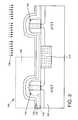
- FIG. 1shows a preliminary structure for one embodiment of a method of providing a dual stress memory technique (SMT) for a semiconductor device 100 .
- the preliminary structureincludes a substrate 102 having an n-type field effect transistor (nFET) 104 and a p-type field effect transistor (pFET) 106 formed thereon.
- semiconductor device 100has completed initial processing such as conventional shallow trench isolation (STI) 110 formation, well implants, gate dielectric 112 formation, gate conductor 114 formation, and extension/halo/source/drain implants for diffusions 116 .
- STIshallow trench isolation
- a first stepincludes forming a tensile stress layer 120 over nFET 104 and a compressive stress layer 122 over pFET 106 .
- Both tensile stress layer 120 and compressive stress layer 122may include intrinsically stressed silicon nitride (Si 3 N 4 ).
- compressive stress layer 122includes a high density plasma (HDP) silicon nitride (Si 3 N 4 ), i.e., a silicon nitride formed using a high density plasma deposition process.
- HDPhigh density plasma
- the compressive stress layer forming stepincludes performing a HDP deposition of silicon nitride using the following conditions: approximately 50 mTorr of pressure, approximately 200 standard cubic centimeters (sccm) of argon (Ar), approximately 100 sccm of silane (SiH 4 ), approximately 300 sccm of nitrogen (N 2 ), approximately 0-1500 W of radio frequency (RF) bias power and approximately 2000W-4500W of RF source power.
- Compressive stress layer 122thus includes a high stress silicon nitride that enables provision of the dual SMT because it allows retention of compressive stress (full or partial) such that the stress is memorized in parts of pFET 106 during the subsequent anneal step, described below.
- a first optional preliminary stepincludes, as shown in FIG. 3 , forming an etch stop layer 118 , e.g., of silicon dioxide (SiO 2 ), (shown in phantom in FIG. 3 only).
- a first sub-stepshown in FIG. 3 includes forming a first stress layer 130 over semiconductor device 100 .
- first stress layer 130may be either tensile stress layer 120 ( FIG. 2 ) or compressive stress layer 122 ( FIG. 2 ). As shown in FIG.
- first stress layer 130includes an intrinsically tensilely stressed silicon nitride.
- a second sub-stepalso shown in FIG. 3 , includes forming an etch stop layer 132 over first stress layer 130 .
- Etch stop layer 132may include any now known or later developed etch stop material such as silicon dioxide (SiO 2 ).
- first stress layer 130 and etch stop layer 132are removed over a first one of nFET 104 and pFET 106 (pFET 106 as shown) to expose one of the FETs.
- the etching 138may include use of a patterned mask 136 (shown in phantom) and any conventional dry etching chemistry for the materials used.
- FIG. 4shows the resulting structure including exposed pFET 106 .
- a second stress layer 140is formed over semiconductor device 100 .
- second stress layer 140is formed over pFET 106 and, hence, includes the above-described high density, compressive stress silicon nitride.
- a next stepmay include removing second stress layer 140 over nFET 104 prior to the annealing step, described below.
- the removing stepmay include use of a patterned mask 146 (shown in phantom) and any conventional dry etching 144 for the materials used.
- FIG. 6shows the resulting structure. Where second stress layer 140 is not removed, it should be recognized that some degradation of stress imparted by first stress layer 130 may be present, but that this degradation is minimal.
- the above-described stepsmay be switched. That is, the forming step may include forming a compressive stress layer 122 over semiconductor device 100 , forming an etch stop layer 132 over the compressive stress layer, removing compressive stress layer 122 and etch stop layer 132 over nFET 104 , and forming a tensile stress layer 120 over semiconductor device 100 .
- tensile stress layer 120may be optionally removed over pFET 106 prior to the annealing step, described below. Where tensile stress layer 120 is not removed, it should be recognized that some degradation of stress imparted by compressive stress layer 122 may be present, but that this degradation is minimal.
- FIG. 6also shows a second step according to one embodiment of the method, which includes annealing 150 to memorize stress in semiconductor device 100 .
- Annealing 150preferably includes using a temperature of no less than approximately 400° C. and no greater than approximately 1200° C. The anneal temperature is optimized so that device 100 will be able to memorize the stress from stress layers 120 , 122 , and not lose the compressive stress on parts of pFET 106 , which would result in a neutral or tensile stress thereon.
- one conventional plasma-enhanced chemical vapor deposited (PECVD) compressive silicon nitridewhich is formed with approximately ⁇ 1.8 GPa of stress drops to approximately 0.04 GPa, i.e., a tensile stress, after anneal.
- PECVDplasma-enhanced chemical vapor deposited
- an HDP compressive stress silicon nitride according to the inventionis formed with approximately ⁇ 3.0 GPa, which results in a stress of no less than ⁇ 100 MPa, thus retaining a compressive stress.
- the compressive stressmay be in the range of approximately ⁇ 1 GPa.
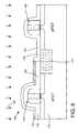
- FIG. 7shows a third step including removing stress layers 120 , 122 and etch stop layer 132 .
- This removing step 148may include a wet or dry etch, or combination of them; for example, a wet or dry etch to remove etch stop layer 132 and then a wet strip using hot phosphorous acid to remove silicon nitride stress layers.
- FIG. 7also shows a semiconductor device 200 according to the invention including an nFET 204 having a tensile stress 260 memorized into a part thereof, e.g., gate conductor 214 and/or diffusion region 216 , and a pFET 206 having a compressive stress 262 memorized into a part thereof, e.g., gate conductor 220 and/or diffusion region 222 .
Landscapes
- Insulated Gate Type Field-Effect Transistor (AREA)
- Metal-Oxide And Bipolar Metal-Oxide Semiconductor Integrated Circuits (AREA)
- Non-Volatile Memory (AREA)
- Chemical Vapour Deposition (AREA)
- Formation Of Insulating Films (AREA)
- Semiconductor Memories (AREA)
Abstract
Description
Claims (13)
Priority Applications (7)
| Application Number | Priority Date | Filing Date | Title |
|---|---|---|---|
| US11/164,114US7785950B2 (en) | 2005-11-10 | 2005-11-10 | Dual stress memory technique method and related structure |
| KR1020060074829AKR100735533B1 (en) | 2005-11-10 | 2006-08-08 | Method of providing a dual stress memory technique and related structure |
| SG200606456-2ASG132585A1 (en) | 2005-11-10 | 2006-09-15 | Dual stress memory technique method and related structure |
| SG200901689-0ASG151256A1 (en) | 2005-11-10 | 2006-09-15 | Dual stress memory technique method and related structure |
| SG200607711-9ASG132607A1 (en) | 2005-11-10 | 2006-11-08 | Dual stress memory technique method and related structure |
| JP2006303401AJP2007134718A (en) | 2005-11-10 | 2006-11-08 | 2-stress memory technology in semiconductor devices |
| CNB2006101463928ACN100570860C (en) | 2005-11-10 | 2006-11-09 | Double stress memory technology method and related semiconductor device |
Applications Claiming Priority (1)
| Application Number | Priority Date | Filing Date | Title |
|---|---|---|---|
| US11/164,114US7785950B2 (en) | 2005-11-10 | 2005-11-10 | Dual stress memory technique method and related structure |
Publications (2)
| Publication Number | Publication Date |
|---|---|
| US20070105299A1 US20070105299A1 (en) | 2007-05-10 |
| US7785950B2true US7785950B2 (en) | 2010-08-31 |
Family
ID=38004289
Family Applications (1)
| Application Number | Title | Priority Date | Filing Date |
|---|---|---|---|
| US11/164,114Expired - Fee RelatedUS7785950B2 (en) | 2005-11-10 | 2005-11-10 | Dual stress memory technique method and related structure |
Country Status (5)
| Country | Link |
|---|---|
| US (1) | US7785950B2 (en) |
| JP (1) | JP2007134718A (en) |
| KR (1) | KR100735533B1 (en) |
| CN (1) | CN100570860C (en) |
| SG (3) | SG132585A1 (en) |
Cited By (6)
| Publication number | Priority date | Publication date | Assignee | Title |
|---|---|---|---|---|
| US20100015766A1 (en)* | 2008-07-21 | 2010-01-21 | Texas Instruments Incorporated | Complementary stress memorization technique layer method |
| US20100117159A1 (en)* | 2006-02-15 | 2010-05-13 | Richard Lindsay | Strained Semiconductor Device and Method of Making Same |
| US9082875B2 (en) | 2009-03-27 | 2015-07-14 | International Business Machines Corporation | Methods for normalizing strain in semicondcutor devices and strain normalized semiconductor devices |
| US9368627B2 (en) | 2014-09-11 | 2016-06-14 | Taiwan Semiconductor Manufacturing Company Ltd. | Semiconductor structure and manufacturing method thereof |
| US9899386B2 (en)* | 2004-03-30 | 2018-02-20 | Samsung Electronics Co., Ltd. | Low noise and high performance LSI device |
| US10892263B2 (en) | 2018-06-15 | 2021-01-12 | Samsung Electronics Co., Ltd. | Methods of fabricating semiconductor device |
Families Citing this family (43)
| Publication number | Priority date | Publication date | Assignee | Title |
|---|---|---|---|---|
| US7785950B2 (en) | 2005-11-10 | 2010-08-31 | International Business Machines Corporation | Dual stress memory technique method and related structure |
| US7332447B2 (en)* | 2005-11-24 | 2008-02-19 | United Microelectronics Corp. | Method of forming a contact |
| JP4899085B2 (en)* | 2006-03-03 | 2012-03-21 | 富士通セミコンダクター株式会社 | Semiconductor device and manufacturing method thereof |
| US7514370B2 (en)* | 2006-05-19 | 2009-04-07 | International Business Machines Corporation | Compressive nitride film and method of manufacturing thereof |
| KR101244590B1 (en)* | 2006-05-31 | 2013-03-25 | 도쿄엘렉트론가부시키가이샤 | Plasma cvd method, method for forming silicon nitride film and method for manufacturing semiconductor device |
| JP5017958B2 (en)* | 2006-08-08 | 2012-09-05 | 富士通セミコンダクター株式会社 | Manufacturing method of semiconductor device |
| US7632729B2 (en)* | 2006-09-27 | 2009-12-15 | Taiwan Semiconductor Manufacturing Co., Ltd. | Method for semiconductor device performance enhancement |
| US7795644B2 (en)* | 2007-01-04 | 2010-09-14 | Taiwan Semiconductor Manufacturing Co., Ltd. | Integrated circuits with stress memory effect and fabrication methods thereof |
| US7759207B2 (en)* | 2007-03-21 | 2010-07-20 | Chartered Semiconductor Manufacturing Ltd. | Integrated circuit system employing stress memorization transfer |
| US20080237734A1 (en)* | 2007-03-29 | 2008-10-02 | United Microelectronics Corp. | Complementary metal-oxide-semiconductor transistor and method of fabricating the same |
| US7611939B2 (en)* | 2007-05-07 | 2009-11-03 | Texas Instruments Incorporated | Semiconductor device manufactured using a laminated stress layer |
| US7834399B2 (en) | 2007-06-05 | 2010-11-16 | International Business Machines Corporation | Dual stress memorization technique for CMOS application |
| US7741168B2 (en)* | 2007-07-25 | 2010-06-22 | Sematech, Inc. | Systems and methods for fabricating nanometric-scale semiconductor devices with dual-stress layers using double-stress oxide/nitride stacks |
| US20090050972A1 (en)* | 2007-08-20 | 2009-02-26 | Richard Lindsay | Strained Semiconductor Device and Method of Making Same |
| JP5117883B2 (en)* | 2008-02-25 | 2013-01-16 | ルネサスエレクトロニクス株式会社 | Manufacturing method of semiconductor device |
| US7767534B2 (en)* | 2008-09-29 | 2010-08-03 | Advanced Micro Devices, Inc. | Methods for fabricating MOS devices having highly stressed channels |
| US8969969B2 (en) | 2009-03-20 | 2015-03-03 | International Business Machines Corporation | High threshold voltage NMOS transistors for low power IC technology |
| US8039349B2 (en)* | 2009-07-30 | 2011-10-18 | Globalfoundries Inc. | Methods for fabricating non-planar semiconductor devices having stress memory |
| CN102054769B (en)* | 2009-10-29 | 2013-03-27 | 中芯国际集成电路制造(上海)有限公司 | Forming method of complementary metal oxide semiconductor (CMOS) structure |
| CN102194749B (en)* | 2010-03-11 | 2013-06-12 | 中芯国际集成电路制造(上海)有限公司 | Method for making complementary type metal-oxide semiconductor device |
| KR20120023968A (en) | 2010-09-03 | 2012-03-14 | 삼성전자주식회사 | Methods of forming transistors, methods of forming cmos transistors and methods of manufacturing semiconductor devices using the same |
| CN102446761B (en)* | 2010-09-30 | 2015-07-15 | 中国科学院微电子研究所 | Method for manufacturing semiconductor structure |
| US9202913B2 (en) | 2010-09-30 | 2015-12-01 | Institute of Microelectronics, Chinese Academy of Sciences | Method for manufacturing semiconductor structure |
| US8535999B2 (en) | 2010-10-12 | 2013-09-17 | International Business Machines Corporation | Stress memorization process improvement for improved technology performance |
| CN102456626B (en)* | 2010-10-20 | 2013-12-18 | 中芯国际集成电路制造(上海)有限公司 | Method for manufacturing semiconductor device based on dual stress liner technology |
| CN102468160A (en)* | 2010-11-03 | 2012-05-23 | 中芯国际集成电路制造(上海)有限公司 | Method for improving narrow channel effect of NFET (N-channel field effect transistor) by utilizing stress memorization technology |
| US8216928B1 (en) | 2011-01-26 | 2012-07-10 | GlobalFoundries, Inc. | Methods for fabricating semiconductor devices having local contacts |
| CN102420119B (en)* | 2011-04-29 | 2013-06-26 | 上海华力微电子有限公司 | Gate polysilicon etching method for enhancing stress memorization technique |
| KR20120136672A (en) | 2011-06-09 | 2012-12-20 | 삼성전자주식회사 | Method for manufacturing semiconductor device |
| CN102446722A (en)* | 2011-08-29 | 2012-05-09 | 上海华力微电子有限公司 | Method for preventing photoresist failure in dual-stress silicon nitride process |
| CN102456565A (en)* | 2011-08-29 | 2012-05-16 | 上海华力微电子有限公司 | Method for preventing photoresist failure in dual-stress silicon nitride process |
| CN103094108B (en)* | 2011-10-29 | 2015-12-02 | 中芯国际集成电路制造(上海)有限公司 | The manufacture method of semiconductor device |
| CN103183307B (en)* | 2011-12-28 | 2016-04-20 | 中国科学院微电子研究所 | Tensile stress LPCVD SiO2Method for producing film |
| CN102709178B (en)* | 2012-05-22 | 2015-08-19 | 上海华力微电子有限公司 | A kind of method forming dual stressed layers silicon nitride film |
| CN103474350A (en)* | 2012-06-06 | 2013-12-25 | 中芯国际集成电路制造(上海)有限公司 | Semiconductor structure and its formation method |
| CN103839800A (en)* | 2012-11-20 | 2014-06-04 | 中国科学院微电子研究所 | Method for producing silicon nitride |
| CN103107239B (en)* | 2012-12-06 | 2016-08-31 | 杭州赛昂电力有限公司 | Heterojunction solar battery and preparation method thereof |
| CN103107234B (en)* | 2012-12-06 | 2016-03-23 | 杭州赛昂电力有限公司 | Heterojunction solar battery and preparation method thereof |
| CN103107236B (en)* | 2012-12-06 | 2016-05-04 | 杭州赛昂电力有限公司 | Heterojunction solar battery and preparation method thereof |
| CN103700631A (en)* | 2013-11-29 | 2014-04-02 | 上海华力微电子有限公司 | Preparation method for non-junction MOS FET (metal oxide semiconductor field effect transistor) device |
| CN104733391A (en)* | 2015-03-31 | 2015-06-24 | 上海华力微电子有限公司 | Semiconductor device manufacturing method |
| KR102426960B1 (en)* | 2015-10-15 | 2022-08-01 | 주식회사 테스 | Method for forming silicon oxide film using plasmas |
| US9941211B1 (en) | 2017-03-24 | 2018-04-10 | International Business Machines Corporation | Reducing metallic interconnect resistivity through application of mechanical strain |
Citations (90)
| Publication number | Priority date | Publication date | Assignee | Title |
|---|---|---|---|---|
| US3602841A (en) | 1970-06-18 | 1971-08-31 | Ibm | High frequency bulk semiconductor amplifiers and oscillators |
| US4665415A (en) | 1985-04-24 | 1987-05-12 | International Business Machines Corporation | Semiconductor device with hole conduction via strained lattice |
| JPS6476755A (en) | 1987-09-18 | 1989-03-22 | Hitachi Ltd | Semiconductor device |
| US4853076A (en) | 1983-12-29 | 1989-08-01 | Massachusetts Institute Of Technology | Semiconductor thin films |
| US4855245A (en) | 1985-09-13 | 1989-08-08 | Siemens Aktiengesellschaft | Method of manufacturing integrated circuit containing bipolar and complementary MOS transistors on a common substrate |
| US4952524A (en) | 1989-05-05 | 1990-08-28 | At&T Bell Laboratories | Semiconductor device manufacture including trench formation |
| US4958213A (en) | 1987-12-07 | 1990-09-18 | Texas Instruments Incorporated | Method for forming a transistor base region under thick oxide |
| US5006913A (en) | 1988-11-05 | 1991-04-09 | Mitsubishi Denki Kabushiki Kaisha | Stacked type semiconductor device |
| US5060030A (en) | 1990-07-18 | 1991-10-22 | Raytheon Company | Pseudomorphic HEMT having strained compensation layer |
| US5081513A (en) | 1991-02-28 | 1992-01-14 | Xerox Corporation | Electronic device with recovery layer proximate to active layer |
| US5108843A (en) | 1988-11-30 | 1992-04-28 | Ricoh Company, Ltd. | Thin film semiconductor and process for producing the same |
| US5134085A (en) | 1991-11-21 | 1992-07-28 | Micron Technology, Inc. | Reduced-mask, split-polysilicon CMOS process, incorporating stacked-capacitor cells, for fabricating multi-megabit dynamic random access memories |
| US5310446A (en) | 1990-01-10 | 1994-05-10 | Ricoh Company, Ltd. | Method for producing semiconductor film |
| US5354695A (en) | 1992-04-08 | 1994-10-11 | Leedy Glenn J | Membrane dielectric isolation IC fabrication |
| US5371399A (en) | 1991-06-14 | 1994-12-06 | International Business Machines Corporation | Compound semiconductor having metallic inclusions and devices fabricated therefrom |
| US5391510A (en) | 1992-02-28 | 1995-02-21 | International Business Machines Corporation | Formation of self-aligned metal gate FETs using a benignant removable gate material during high temperature steps |
| US5459346A (en) | 1988-06-28 | 1995-10-17 | Ricoh Co., Ltd. | Semiconductor substrate with electrical contact in groove |
| US5557122A (en) | 1995-05-12 | 1996-09-17 | Alliance Semiconductors Corporation | Semiconductor electrode having improved grain structure and oxide growth properties |
| US5561302A (en) | 1994-09-26 | 1996-10-01 | Motorola, Inc. | Enhanced mobility MOSFET device and method |
| US5670798A (en) | 1995-03-29 | 1997-09-23 | North Carolina State University | Integrated heterostructures of Group III-V nitride semiconductor materials including epitaxial ohmic contact non-nitride buffer layer and methods of fabricating same |
| US5679965A (en) | 1995-03-29 | 1997-10-21 | North Carolina State University | Integrated heterostructures of Group III-V nitride semiconductor materials including epitaxial ohmic contact, non-nitride buffer layer and methods of fabricating same |
| US5861651A (en) | 1997-02-28 | 1999-01-19 | Lucent Technologies Inc. | Field effect devices and capacitors with improved thin film dielectrics and method for making same |
| US5880040A (en) | 1996-04-15 | 1999-03-09 | Macronix International Co., Ltd. | Gate dielectric based on oxynitride grown in N2 O and annealed in NO |
| US5940736A (en) | 1997-03-11 | 1999-08-17 | Lucent Technologies Inc. | Method for forming a high quality ultrathin gate oxide layer |
| US5940716A (en) | 1996-03-15 | 1999-08-17 | Samsung Electronics Co., Ltd. | Methods of forming trench isolation regions using repatterned trench masks |
| US5960297A (en) | 1997-07-02 | 1999-09-28 | Kabushiki Kaisha Toshiba | Shallow trench isolation structure and method of forming the same |
| US5989978A (en) | 1998-07-16 | 1999-11-23 | Chartered Semiconductor Manufacturing, Ltd. | Shallow trench isolation of MOSFETS with reduced corner parasitic currents |
| US6008126A (en) | 1992-04-08 | 1999-12-28 | Elm Technology Corporation | Membrane dielectric isolation IC fabrication |
| US6025280A (en) | 1997-04-28 | 2000-02-15 | Lucent Technologies Inc. | Use of SiD4 for deposition of ultra thin and controllable oxides |
| US6066545A (en) | 1997-12-09 | 2000-05-23 | Texas Instruments Incorporated | Birdsbeak encroachment using combination of wet and dry etch for isolation nitride |
| US6090684A (en) | 1998-07-31 | 2000-07-18 | Hitachi, Ltd. | Method for manufacturing semiconductor device |
| US6107143A (en) | 1998-03-02 | 2000-08-22 | Samsung Electronics Co., Ltd. | Method for forming a trench isolation structure in an integrated circuit |
| US6117722A (en) | 1999-02-18 | 2000-09-12 | Taiwan Semiconductor Manufacturing Company | SRAM layout for relaxing mechanical stress in shallow trench isolation technology and method of manufacture thereof |
| US6133071A (en) | 1997-10-15 | 2000-10-17 | Nec Corporation | Semiconductor device with plate heat sink free from cracks due to thermal stress and process for assembling it with package |
| US6165383A (en) | 1998-04-10 | 2000-12-26 | Organic Display Technology | Useful precursors for organic electroluminescent materials and devices made from such materials |
| US6221735B1 (en) | 2000-02-15 | 2001-04-24 | Philips Semiconductors, Inc. | Method for eliminating stress induced dislocations in CMOS devices |
| US6228694B1 (en) | 1999-06-28 | 2001-05-08 | Intel Corporation | Method of increasing the mobility of MOS transistors by use of localized stress regions |
| US6255169B1 (en) | 1999-02-22 | 2001-07-03 | Advanced Micro Devices, Inc. | Process for fabricating a high-endurance non-volatile memory device |
| US6261964B1 (en) | 1997-03-14 | 2001-07-17 | Micron Technology, Inc. | Material removal method for forming a structure |
| US6265317B1 (en) | 2001-01-09 | 2001-07-24 | Taiwan Semiconductor Manufacturing Company | Top corner rounding for shallow trench isolation |
| US20010009784A1 (en) | 1998-01-09 | 2001-07-26 | Yanjun Ma | Structure and method of making a sub-micron MOS transistor |
| US6274444B1 (en) | 1999-07-30 | 2001-08-14 | United Microelectronics Corp. | Method for forming mosfet |
| US6281532B1 (en) | 1999-06-28 | 2001-08-28 | Intel Corporation | Technique to obtain increased channel mobilities in NMOS transistors by gate electrode engineering |
| US6284623B1 (en) | 1999-10-25 | 2001-09-04 | Peng-Fei Zhang | Method of fabricating semiconductor devices using shallow trench isolation with reduced narrow channel effect |
| US6284626B1 (en) | 1999-04-06 | 2001-09-04 | Vantis Corporation | Angled nitrogen ion implantation for minimizing mechanical stress on side walls of an isolation trench |
| US6319794B1 (en) | 1998-10-14 | 2001-11-20 | International Business Machines Corporation | Structure and method for producing low leakage isolation devices |
| US6362082B1 (en) | 1999-06-28 | 2002-03-26 | Intel Corporation | Methodology for control of short channel effects in MOS transistors |
| US6361885B1 (en) | 1998-04-10 | 2002-03-26 | Organic Display Technology | Organic electroluminescent materials and device made from such materials |
| US6368931B1 (en) | 2000-03-27 | 2002-04-09 | Intel Corporation | Thin tensile layers in shallow trench isolation and method of making same |
| US6372291B1 (en)* | 1999-12-23 | 2002-04-16 | Applied Materials, Inc. | In situ deposition and integration of silicon nitride in a high density plasma reactor |
| US20020063292A1 (en) | 2000-11-29 | 2002-05-30 | Mark Armstrong | CMOS fabrication process utilizing special transistor orientation |
| US6403975B1 (en) | 1996-04-09 | 2002-06-11 | Max-Planck Gesellschaft Zur Forderung Der Wissenschafteneev | Semiconductor components, in particular photodetectors, light emitting diodes, optical modulators and waveguides with multilayer structures grown on silicon substrates |
| US6403486B1 (en) | 2001-04-30 | 2002-06-11 | Taiwan Semiconductor Manufacturing Company | Method for forming a shallow trench isolation |
| US6406973B1 (en) | 1999-06-29 | 2002-06-18 | Hyundai Electronics Industries Co., Ltd. | Transistor in a semiconductor device and method of manufacturing the same |
| US20020086497A1 (en) | 2000-12-30 | 2002-07-04 | Kwok Siang Ping | Beaker shape trench with nitride pull-back for STI |
| US20020086472A1 (en) | 2000-12-29 | 2002-07-04 | Brian Roberds | Technique to obtain high mobility channels in MOS transistors by forming a strain layer on an underside of a channel |
| US20020090791A1 (en) | 1999-06-28 | 2002-07-11 | Brian S. Doyle | Method for reduced capacitance interconnect system using gaseous implants into the ild |
| US6461936B1 (en) | 2002-01-04 | 2002-10-08 | Infineon Technologies Ag | Double pullback method of filling an isolation trench |
| US6476462B2 (en) | 1999-12-28 | 2002-11-05 | Texas Instruments Incorporated | MOS-type semiconductor device and method for making same |
| US6483171B1 (en) | 1999-08-13 | 2002-11-19 | Micron Technology, Inc. | Vertical sub-micron CMOS transistors on (110), (111), (311), (511), and higher order surfaces of bulk, SOI and thin film structures and method of forming same |
| US6493497B1 (en) | 2000-09-26 | 2002-12-10 | Motorola, Inc. | Electro-optic structure and process for fabricating same |
| US6498358B1 (en) | 2001-07-20 | 2002-12-24 | Motorola, Inc. | Structure and method for fabricating an electro-optic system having an electrochromic diffraction grating |
| US6501121B1 (en) | 2000-11-15 | 2002-12-31 | Motorola, Inc. | Semiconductor structure |
| US6506652B2 (en) | 1998-11-13 | 2003-01-14 | Intel Corporation | Method of recessing spacers to improved salicide resistance on polysilicon gates |
| US20030032261A1 (en) | 2001-08-08 | 2003-02-13 | Ling-Yen Yeh | Method of preventing threshold voltage of MOS transistor from being decreased by shallow trench isolation formation |
| US20030040158A1 (en) | 2001-08-21 | 2003-02-27 | Nec Corporation | Semiconductor device and method of fabricating the same |
| US6531369B1 (en) | 2000-03-01 | 2003-03-11 | Applied Micro Circuits Corporation | Heterojunction bipolar transistor (HBT) fabrication using a selectively deposited silicon germanium (SiGe) |
| US6531740B2 (en) | 2001-07-17 | 2003-03-11 | Motorola, Inc. | Integrated impedance matching and stability network |
| US20030057184A1 (en) | 2001-09-22 | 2003-03-27 | Shiuh-Sheng Yu | Method for pull back SiN to increase rounding effect in a shallow trench isolation process |
| US20030067035A1 (en) | 2001-09-28 | 2003-04-10 | Helmut Tews | Gate processing method with reduced gate oxide corner and edge thinning |
| US6621392B1 (en) | 2002-04-25 | 2003-09-16 | International Business Machines Corporation | Micro electromechanical switch having self-aligned spacers |
| US6635506B2 (en) | 2001-11-07 | 2003-10-21 | International Business Machines Corporation | Method of fabricating micro-electromechanical switches on CMOS compatible substrates |
| US20040029323A1 (en)* | 2000-11-22 | 2004-02-12 | Akihiro Shimizu | Semiconductor device and method for fabricating the same |
| US6717216B1 (en) | 2002-12-12 | 2004-04-06 | International Business Machines Corporation | SOI based field effect transistor having a compressive film in undercut area under the channel and a method of making the device |
| US20040113174A1 (en)* | 2002-12-12 | 2004-06-17 | International Business Machines Corporation | Isolation structures for imposing stress patterns |
| US6831292B2 (en) | 2001-09-21 | 2004-12-14 | Amberwave Systems Corporation | Semiconductor structures employing strained material layers with defined impurity gradients and methods for fabricating same |
| US6881665B1 (en)* | 2000-08-09 | 2005-04-19 | Advanced Micro Devices, Inc. | Depth of focus (DOF) for trench-first-via-last (TFVL) damascene processing with hard mask and low viscosity photoresist |
| US20050093059A1 (en)* | 2003-10-30 | 2005-05-05 | Belyansky Michael P. | Structure and method to improve channel mobility by gate electrode stress modification |
| US20050093081A1 (en)* | 2003-11-04 | 2005-05-05 | Internatioanal Business Machines Corporation | Oxidation method for altering a film structure and cmos transistor structure formed therewith |
| US20050156208A1 (en)* | 2003-09-30 | 2005-07-21 | Taiwan Semiconductor Manufacturing Company, Ltd. | Device having multiple silicide types and a method for its fabrication |
| US20050194596A1 (en) | 2003-10-30 | 2005-09-08 | Victor Chan | Increasing carrier mobility in NFET and PFET transistors on a common wafer |
| US20050199958A1 (en)* | 2004-03-10 | 2005-09-15 | Taiwan Semiconductor Manufacturing Co., Ltd. | Method for selectively stressing MOSFETs to improve charge carrier mobility |
| US20060091471A1 (en)* | 2004-10-29 | 2006-05-04 | Kai Frohberg | Technique for creating different mechanical strain in different channel regions by forming an etch stop layer stack having differently modified intrinsic stress |
| US20060148270A1 (en)* | 2005-01-05 | 2006-07-06 | Wei Lu | High density plasma and bias RF power process to make stable FSG with less free F and SiN with less H to enhance the FSG/SiN integration reliability |
| US20060228848A1 (en)* | 2005-03-31 | 2006-10-12 | International Business Machines Corporation | Dual-hybrid liner formation without exposing silicide layer to photoresist stripping chemicals |
| US20070010073A1 (en)* | 2005-07-06 | 2007-01-11 | Chien-Hao Chen | Method of forming a MOS device having a strained channel region |
| US20070018252A1 (en)* | 2005-07-21 | 2007-01-25 | International Business Machines Corporation | Semiconductor device containing high performance p-mosfet and/or n-mosfet and method of fabricating the same |
| US20070040225A1 (en)* | 2005-08-22 | 2007-02-22 | Yang Haining S | High performance MOSFET comprising a stressed gate metal silicide layer and method of fabricating the same |
| US20070075360A1 (en)* | 2005-09-30 | 2007-04-05 | Alpha &Omega Semiconductor, Ltd. | Cobalt silicon contact barrier metal process for high density semiconductor power devices |
| US20070105299A1 (en) | 2005-11-10 | 2007-05-10 | International Business Machines Corporation | Dual stress memory technique method and related structure |
- 2005
- 2005-11-10USUS11/164,114patent/US7785950B2/ennot_activeExpired - Fee Related
- 2006
- 2006-08-08KRKR1020060074829Apatent/KR100735533B1/enactiveActive
- 2006-09-15SGSG200606456-2Apatent/SG132585A1/enunknown
- 2006-09-15SGSG200901689-0Apatent/SG151256A1/enunknown
- 2006-11-08JPJP2006303401Apatent/JP2007134718A/enactivePending
- 2006-11-08SGSG200607711-9Apatent/SG132607A1/enunknown
- 2006-11-09CNCNB2006101463928Apatent/CN100570860C/ennot_activeExpired - Fee Related
Patent Citations (105)
| Publication number | Priority date | Publication date | Assignee | Title |
|---|---|---|---|---|
| US3602841A (en) | 1970-06-18 | 1971-08-31 | Ibm | High frequency bulk semiconductor amplifiers and oscillators |
| US4853076A (en) | 1983-12-29 | 1989-08-01 | Massachusetts Institute Of Technology | Semiconductor thin films |
| US4665415A (en) | 1985-04-24 | 1987-05-12 | International Business Machines Corporation | Semiconductor device with hole conduction via strained lattice |
| US4855245A (en) | 1985-09-13 | 1989-08-08 | Siemens Aktiengesellschaft | Method of manufacturing integrated circuit containing bipolar and complementary MOS transistors on a common substrate |
| JPS6476755A (en) | 1987-09-18 | 1989-03-22 | Hitachi Ltd | Semiconductor device |
| US4958213A (en) | 1987-12-07 | 1990-09-18 | Texas Instruments Incorporated | Method for forming a transistor base region under thick oxide |
| US5565697A (en) | 1988-06-28 | 1996-10-15 | Ricoh Company, Ltd. | Semiconductor structure having island forming grooves |
| US5459346A (en) | 1988-06-28 | 1995-10-17 | Ricoh Co., Ltd. | Semiconductor substrate with electrical contact in groove |
| US5006913A (en) | 1988-11-05 | 1991-04-09 | Mitsubishi Denki Kabushiki Kaisha | Stacked type semiconductor device |
| US5108843A (en) | 1988-11-30 | 1992-04-28 | Ricoh Company, Ltd. | Thin film semiconductor and process for producing the same |
| US4952524A (en) | 1989-05-05 | 1990-08-28 | At&T Bell Laboratories | Semiconductor device manufacture including trench formation |
| US5310446A (en) | 1990-01-10 | 1994-05-10 | Ricoh Company, Ltd. | Method for producing semiconductor film |
| US5060030A (en) | 1990-07-18 | 1991-10-22 | Raytheon Company | Pseudomorphic HEMT having strained compensation layer |
| US5081513A (en) | 1991-02-28 | 1992-01-14 | Xerox Corporation | Electronic device with recovery layer proximate to active layer |
| US5371399A (en) | 1991-06-14 | 1994-12-06 | International Business Machines Corporation | Compound semiconductor having metallic inclusions and devices fabricated therefrom |
| US5471948A (en) | 1991-06-14 | 1995-12-05 | International Business Machines Corporation | Method of making a compound semiconductor having metallic inclusions |
| US5134085A (en) | 1991-11-21 | 1992-07-28 | Micron Technology, Inc. | Reduced-mask, split-polysilicon CMOS process, incorporating stacked-capacitor cells, for fabricating multi-megabit dynamic random access memories |
| US5391510A (en) | 1992-02-28 | 1995-02-21 | International Business Machines Corporation | Formation of self-aligned metal gate FETs using a benignant removable gate material during high temperature steps |
| US6008126A (en) | 1992-04-08 | 1999-12-28 | Elm Technology Corporation | Membrane dielectric isolation IC fabrication |
| US5354695A (en) | 1992-04-08 | 1994-10-11 | Leedy Glenn J | Membrane dielectric isolation IC fabrication |
| US5946559A (en) | 1992-04-08 | 1999-08-31 | Elm Technology Corporation | Membrane dielectric isolation IC fabrication |
| US5571741A (en) | 1992-04-08 | 1996-11-05 | Leedy; Glenn J. | Membrane dielectric isolation IC fabrication |
| US5592007A (en) | 1992-04-08 | 1997-01-07 | Leedy; Glenn J. | Membrane dielectric isolation transistor fabrication |
| US5592018A (en) | 1992-04-08 | 1997-01-07 | Leedy; Glenn J. | Membrane dielectric isolation IC fabrication |
| US5840593A (en) | 1992-04-08 | 1998-11-24 | Elm Technology Corporation | Membrane dielectric isolation IC fabrication |
| US5683934A (en) | 1994-09-26 | 1997-11-04 | Motorola, Inc. | Enhanced mobility MOSFET device and method |
| US5561302A (en) | 1994-09-26 | 1996-10-01 | Motorola, Inc. | Enhanced mobility MOSFET device and method |
| US5679965A (en) | 1995-03-29 | 1997-10-21 | North Carolina State University | Integrated heterostructures of Group III-V nitride semiconductor materials including epitaxial ohmic contact, non-nitride buffer layer and methods of fabricating same |
| US5670798A (en) | 1995-03-29 | 1997-09-23 | North Carolina State University | Integrated heterostructures of Group III-V nitride semiconductor materials including epitaxial ohmic contact non-nitride buffer layer and methods of fabricating same |
| US6046464A (en) | 1995-03-29 | 2000-04-04 | North Carolina State University | Integrated heterostructures of group III-V nitride semiconductor materials including epitaxial ohmic contact comprising multiple quantum well |
| US5557122A (en) | 1995-05-12 | 1996-09-17 | Alliance Semiconductors Corporation | Semiconductor electrode having improved grain structure and oxide growth properties |
| US5940716A (en) | 1996-03-15 | 1999-08-17 | Samsung Electronics Co., Ltd. | Methods of forming trench isolation regions using repatterned trench masks |
| US6403975B1 (en) | 1996-04-09 | 2002-06-11 | Max-Planck Gesellschaft Zur Forderung Der Wissenschafteneev | Semiconductor components, in particular photodetectors, light emitting diodes, optical modulators and waveguides with multilayer structures grown on silicon substrates |
| US5880040A (en) | 1996-04-15 | 1999-03-09 | Macronix International Co., Ltd. | Gate dielectric based on oxynitride grown in N2 O and annealed in NO |
| US5861651A (en) | 1997-02-28 | 1999-01-19 | Lucent Technologies Inc. | Field effect devices and capacitors with improved thin film dielectrics and method for making same |
| US6246095B1 (en) | 1997-03-11 | 2001-06-12 | Agere Systems Guardian Corp. | System and method for forming a uniform thin gate oxide layer |
| US5940736A (en) | 1997-03-11 | 1999-08-17 | Lucent Technologies Inc. | Method for forming a high quality ultrathin gate oxide layer |
| US6261964B1 (en) | 1997-03-14 | 2001-07-17 | Micron Technology, Inc. | Material removal method for forming a structure |
| US6025280A (en) | 1997-04-28 | 2000-02-15 | Lucent Technologies Inc. | Use of SiD4 for deposition of ultra thin and controllable oxides |
| US5960297A (en) | 1997-07-02 | 1999-09-28 | Kabushiki Kaisha Toshiba | Shallow trench isolation structure and method of forming the same |
| US6133071A (en) | 1997-10-15 | 2000-10-17 | Nec Corporation | Semiconductor device with plate heat sink free from cracks due to thermal stress and process for assembling it with package |
| US6066545A (en) | 1997-12-09 | 2000-05-23 | Texas Instruments Incorporated | Birdsbeak encroachment using combination of wet and dry etch for isolation nitride |
| US20010009784A1 (en) | 1998-01-09 | 2001-07-26 | Yanjun Ma | Structure and method of making a sub-micron MOS transistor |
| US6107143A (en) | 1998-03-02 | 2000-08-22 | Samsung Electronics Co., Ltd. | Method for forming a trench isolation structure in an integrated circuit |
| US6361885B1 (en) | 1998-04-10 | 2002-03-26 | Organic Display Technology | Organic electroluminescent materials and device made from such materials |
| US6165383A (en) | 1998-04-10 | 2000-12-26 | Organic Display Technology | Useful precursors for organic electroluminescent materials and devices made from such materials |
| US5989978A (en) | 1998-07-16 | 1999-11-23 | Chartered Semiconductor Manufacturing, Ltd. | Shallow trench isolation of MOSFETS with reduced corner parasitic currents |
| US6090684A (en) | 1998-07-31 | 2000-07-18 | Hitachi, Ltd. | Method for manufacturing semiconductor device |
| US6319794B1 (en) | 1998-10-14 | 2001-11-20 | International Business Machines Corporation | Structure and method for producing low leakage isolation devices |
| US6509618B2 (en) | 1998-11-13 | 2003-01-21 | Intel Corporation | Device having thin first spacers and partially recessed thick second spacers for improved salicide resistance on polysilicon gates |
| US6521964B1 (en) | 1998-11-13 | 2003-02-18 | Intel Corporation | Device having spacers for improved salicide resistance on polysilicon gates |
| US6506652B2 (en) | 1998-11-13 | 2003-01-14 | Intel Corporation | Method of recessing spacers to improved salicide resistance on polysilicon gates |
| US6117722A (en) | 1999-02-18 | 2000-09-12 | Taiwan Semiconductor Manufacturing Company | SRAM layout for relaxing mechanical stress in shallow trench isolation technology and method of manufacture thereof |
| US6255169B1 (en) | 1999-02-22 | 2001-07-03 | Advanced Micro Devices, Inc. | Process for fabricating a high-endurance non-volatile memory device |
| US6284626B1 (en) | 1999-04-06 | 2001-09-04 | Vantis Corporation | Angled nitrogen ion implantation for minimizing mechanical stress on side walls of an isolation trench |
| US6281532B1 (en) | 1999-06-28 | 2001-08-28 | Intel Corporation | Technique to obtain increased channel mobilities in NMOS transistors by gate electrode engineering |
| US6362082B1 (en) | 1999-06-28 | 2002-03-26 | Intel Corporation | Methodology for control of short channel effects in MOS transistors |
| US6228694B1 (en) | 1999-06-28 | 2001-05-08 | Intel Corporation | Method of increasing the mobility of MOS transistors by use of localized stress regions |
| US20020090791A1 (en) | 1999-06-28 | 2002-07-11 | Brian S. Doyle | Method for reduced capacitance interconnect system using gaseous implants into the ild |
| US20020074598A1 (en) | 1999-06-28 | 2002-06-20 | Doyle Brian S. | Methodology for control of short channel effects in MOS transistors |
| US6406973B1 (en) | 1999-06-29 | 2002-06-18 | Hyundai Electronics Industries Co., Ltd. | Transistor in a semiconductor device and method of manufacturing the same |
| US6274444B1 (en) | 1999-07-30 | 2001-08-14 | United Microelectronics Corp. | Method for forming mosfet |
| US6483171B1 (en) | 1999-08-13 | 2002-11-19 | Micron Technology, Inc. | Vertical sub-micron CMOS transistors on (110), (111), (311), (511), and higher order surfaces of bulk, SOI and thin film structures and method of forming same |
| US6284623B1 (en) | 1999-10-25 | 2001-09-04 | Peng-Fei Zhang | Method of fabricating semiconductor devices using shallow trench isolation with reduced narrow channel effect |
| US6372291B1 (en)* | 1999-12-23 | 2002-04-16 | Applied Materials, Inc. | In situ deposition and integration of silicon nitride in a high density plasma reactor |
| US6476462B2 (en) | 1999-12-28 | 2002-11-05 | Texas Instruments Incorporated | MOS-type semiconductor device and method for making same |
| US6221735B1 (en) | 2000-02-15 | 2001-04-24 | Philips Semiconductors, Inc. | Method for eliminating stress induced dislocations in CMOS devices |
| US6531369B1 (en) | 2000-03-01 | 2003-03-11 | Applied Micro Circuits Corporation | Heterojunction bipolar transistor (HBT) fabrication using a selectively deposited silicon germanium (SiGe) |
| US6368931B1 (en) | 2000-03-27 | 2002-04-09 | Intel Corporation | Thin tensile layers in shallow trench isolation and method of making same |
| US6881665B1 (en)* | 2000-08-09 | 2005-04-19 | Advanced Micro Devices, Inc. | Depth of focus (DOF) for trench-first-via-last (TFVL) damascene processing with hard mask and low viscosity photoresist |
| US6493497B1 (en) | 2000-09-26 | 2002-12-10 | Motorola, Inc. | Electro-optic structure and process for fabricating same |
| US6501121B1 (en) | 2000-11-15 | 2002-12-31 | Motorola, Inc. | Semiconductor structure |
| US20040029323A1 (en)* | 2000-11-22 | 2004-02-12 | Akihiro Shimizu | Semiconductor device and method for fabricating the same |
| US20020063292A1 (en) | 2000-11-29 | 2002-05-30 | Mark Armstrong | CMOS fabrication process utilizing special transistor orientation |
| US20020086472A1 (en) | 2000-12-29 | 2002-07-04 | Brian Roberds | Technique to obtain high mobility channels in MOS transistors by forming a strain layer on an underside of a channel |
| US20020086497A1 (en) | 2000-12-30 | 2002-07-04 | Kwok Siang Ping | Beaker shape trench with nitride pull-back for STI |
| US6265317B1 (en) | 2001-01-09 | 2001-07-24 | Taiwan Semiconductor Manufacturing Company | Top corner rounding for shallow trench isolation |
| US6403486B1 (en) | 2001-04-30 | 2002-06-11 | Taiwan Semiconductor Manufacturing Company | Method for forming a shallow trench isolation |
| US6531740B2 (en) | 2001-07-17 | 2003-03-11 | Motorola, Inc. | Integrated impedance matching and stability network |
| US6498358B1 (en) | 2001-07-20 | 2002-12-24 | Motorola, Inc. | Structure and method for fabricating an electro-optic system having an electrochromic diffraction grating |
| US20030032261A1 (en) | 2001-08-08 | 2003-02-13 | Ling-Yen Yeh | Method of preventing threshold voltage of MOS transistor from being decreased by shallow trench isolation formation |
| US20030040158A1 (en) | 2001-08-21 | 2003-02-27 | Nec Corporation | Semiconductor device and method of fabricating the same |
| US6831292B2 (en) | 2001-09-21 | 2004-12-14 | Amberwave Systems Corporation | Semiconductor structures employing strained material layers with defined impurity gradients and methods for fabricating same |
| US20030057184A1 (en) | 2001-09-22 | 2003-03-27 | Shiuh-Sheng Yu | Method for pull back SiN to increase rounding effect in a shallow trench isolation process |
| US20030067035A1 (en) | 2001-09-28 | 2003-04-10 | Helmut Tews | Gate processing method with reduced gate oxide corner and edge thinning |
| US6635506B2 (en) | 2001-11-07 | 2003-10-21 | International Business Machines Corporation | Method of fabricating micro-electromechanical switches on CMOS compatible substrates |
| US6461936B1 (en) | 2002-01-04 | 2002-10-08 | Infineon Technologies Ag | Double pullback method of filling an isolation trench |
| US6621392B1 (en) | 2002-04-25 | 2003-09-16 | International Business Machines Corporation | Micro electromechanical switch having self-aligned spacers |
| US6717216B1 (en) | 2002-12-12 | 2004-04-06 | International Business Machines Corporation | SOI based field effect transistor having a compressive film in undercut area under the channel and a method of making the device |
| US20040113174A1 (en)* | 2002-12-12 | 2004-06-17 | International Business Machines Corporation | Isolation structures for imposing stress patterns |
| US20050156208A1 (en)* | 2003-09-30 | 2005-07-21 | Taiwan Semiconductor Manufacturing Company, Ltd. | Device having multiple silicide types and a method for its fabrication |
| US20050093059A1 (en)* | 2003-10-30 | 2005-05-05 | Belyansky Michael P. | Structure and method to improve channel mobility by gate electrode stress modification |
| US20050194596A1 (en) | 2003-10-30 | 2005-09-08 | Victor Chan | Increasing carrier mobility in NFET and PFET transistors on a common wafer |
| US20050093081A1 (en)* | 2003-11-04 | 2005-05-05 | Internatioanal Business Machines Corporation | Oxidation method for altering a film structure and cmos transistor structure formed therewith |
| US20050199958A1 (en)* | 2004-03-10 | 2005-09-15 | Taiwan Semiconductor Manufacturing Co., Ltd. | Method for selectively stressing MOSFETs to improve charge carrier mobility |
| US20060091471A1 (en)* | 2004-10-29 | 2006-05-04 | Kai Frohberg | Technique for creating different mechanical strain in different channel regions by forming an etch stop layer stack having differently modified intrinsic stress |
| US20060148270A1 (en)* | 2005-01-05 | 2006-07-06 | Wei Lu | High density plasma and bias RF power process to make stable FSG with less free F and SiN with less H to enhance the FSG/SiN integration reliability |
| US20060228848A1 (en)* | 2005-03-31 | 2006-10-12 | International Business Machines Corporation | Dual-hybrid liner formation without exposing silicide layer to photoresist stripping chemicals |
| US20070010073A1 (en)* | 2005-07-06 | 2007-01-11 | Chien-Hao Chen | Method of forming a MOS device having a strained channel region |
| US20070018252A1 (en)* | 2005-07-21 | 2007-01-25 | International Business Machines Corporation | Semiconductor device containing high performance p-mosfet and/or n-mosfet and method of fabricating the same |
| US20070040225A1 (en)* | 2005-08-22 | 2007-02-22 | Yang Haining S | High performance MOSFET comprising a stressed gate metal silicide layer and method of fabricating the same |
| US20070075360A1 (en)* | 2005-09-30 | 2007-04-05 | Alpha &Omega Semiconductor, Ltd. | Cobalt silicon contact barrier metal process for high density semiconductor power devices |
| US20070105299A1 (en) | 2005-11-10 | 2007-05-10 | International Business Machines Corporation | Dual stress memory technique method and related structure |
| SG132585A1 (en) | 2005-11-10 | 2007-06-28 | Chartered Semiconductor Mfg | Dual stress memory technique method and related structure |
| SG151256A1 (en) | 2005-11-10 | 2009-04-30 | Chartered Semiconductor Mfg | Dual stress memory technique method and related structure |
Non-Patent Citations (25)
| Title |
|---|
| A. Shimizu, et al., "Local Mechanical-Stress Control (LMC): A New Technique for CMOS-Performance Enhancement." International Electron Devices Meeting, IEEE, Mar. 2001. |
| B. Doyle, et al., "Recovery of Hot-Carrier Damage in Reoxidized Nitrided Oxide MOSFETs." IEEE Electron Device Letters, vol. 13, No. 1, Jan. 1992, pp. 38-40. |
| C.J. Huang, et al., "Temperature Dependence and Post-Stress Recovery of Hot Electron Degradation Effects in Bipolar Transistors." IEEE 1991 Bipolar Circuits and Technology Meeting 7.5, pp. 170-173. |
| Chen et al., "Stress Memorization Technique (SMT) by Selectively Strained-Nitride Capping for Sub-65nm High-Performance Strained-Si Device Application," Symposium on VLSI Technology Digest of Technical Papers, pp. 56-57, 2004. |
| D.C. Houghton, et al., "Equilibrium Critical Thickness for SI 1-x GEx Strained Layers on (100) Si". Appl. Phys. Lett. 56 (5) , Jan. 29, 1990, pp. 460-462. |
| F. Ootsuka, et al., "A Highly Dense, High-Performance 130nm Node CMOS Technology for Large Scale System-on-a-Chip Application." International Electron Devices Meeting, 23.5.1, IEEE, Apr. 2000. |
| G. Zhang, et al., "A New 'Mixed-Mode' Reliability Degradation Mechanism in Advanced Si and SiGe Bipolar Transistors." IEEE Transactions on Electron Devices, vol. 49, No. 12, Dec. 2002, pp. 2151-2156. |
| Gregory Scott, et al., "NMOS Drive Current Reduction Caused by Transistor Layout and Trench Isolation Induced Stress." International Electron Devices Meeting, 34.4.1, IEEE, Sep. 1999. |
| H. Li, et al., "Design of W-Band VCOs with High Output Power for Potential Application in 77 GHz Automotive Radar Systems." 2003 IEEE GaAs Digest, pp. 263-266. |
| H. Wurzer, et al., "Annealing of Degraded mpn-Transistors- Mechanisms and Modeling." IEEE Transactions on Electron Devices, vol. 41, No. 4, Apr. 1994, pp. 533-538. |
| H.S. Momose, et al., "Analysis of the Temperature Dependence of Hot-Carrier-Induced Degradation in Bipolar Transistors for Bi-CMOS." IEEE Transactions on Electron Devices, vol. 41, No. 6, Jun. 1994, pp. 978-987. |
| H.S. Momose, et al., "Temperature Dewndence of Emitter-Base Reverse Stress Degradation and its Mechanism Analyzed by MOS Structures." Paper 6.2, pp. 140-143. |
| IPOS International Search Report with Written Opinion, Jul. 15, 2009, 11 pages. |
| J.C. Bean, et al., "GEx SI 1-x/Si Strained-Layer Superlattice Grown by Molecular Beam Epitaxy". J. Vac. Sci. Technol. A 2(2), Apr.-Jun. 1984, pp. 436-440. |
| J.H. Van Der Nerve, "Regular Articles". Journal of Applied Physics, vol. 34, No. 1, Jan. 1963, pp. 117-122. |
| J.W. Matthews, et al., "Defects in Epitaxial Multilayers". Journal of Crystal Growth 27 (1974), pp. 118-125. |
| K. Ota, et al., "Novel Locally Strained Channel Technique for High Performance 55nm CMOS." International Electron Devices Meeting, 2.2.1, IEEE, Feb. 2002. |
| Kern Rim, et al., "Characteristics and Device Design of Sub-100 nm Strained Si N- and PMOSFETs." 2002 Symposium on VLSI Technology Digest of Technical Papers, IEEE, pp. 98-99. |
| Kern Rim, et al., "Transconductance Enhancement in Deep Submicron Strained-Si n-MOSFETs". International Electron Devices Meeting, 26, 8, 1, IEEE, Sep. 1998. |
| M. Khater, et al., "SiGe HBT Technology with Fmax/Ft=350/300 GHz and Gate Delay Below 3.3 ps", 2004 IEEE, 4 pages. |
| R.H.M. Van De Leur, et al., "Critical Thickness for Pseudomorphic Growth of Si/Ge Alloys and Superlattices". J. Appl. Phys. 64 (6), Sep. 15, 1988, pp. 3043-3050. |
| S.R. Sheng, et al., "Degradation and Recovery of SiGe HBTs Following Radiation and Hot-Carrier Stressing." pp. 14-15. |
| Shinya Ito, et al., "Mechanical Stress Effect of Etch-Stop Nitride and Its Impact on Deep Submicron Transistor Design." International Electron Devices Meeting, 10.7.1, IEEE, Apr. 2000. |
| Subramanian S. Iyer, et al., "Heterojunction Bipolar Transistors Using Si-Ge Alloys". IEEE Transactions on Electron Devices, vol. 36, No. 10, Oct. 1989, pp. 2043-2064. |
| Z. Yang, et al., "Avalanche Current Induced Hot Carrier Degradation in 200 GHz SiGe Heterojunction Bipolar Transistors." pp. 1-5. |
Cited By (9)
| Publication number | Priority date | Publication date | Assignee | Title |
|---|---|---|---|---|
| US9899386B2 (en)* | 2004-03-30 | 2018-02-20 | Samsung Electronics Co., Ltd. | Low noise and high performance LSI device |
| US20100117159A1 (en)* | 2006-02-15 | 2010-05-13 | Richard Lindsay | Strained Semiconductor Device and Method of Making Same |
| US8482042B2 (en)* | 2006-02-15 | 2013-07-09 | Infineon Technologies Ag | Strained semiconductor device and method of making same |
| US20100015766A1 (en)* | 2008-07-21 | 2010-01-21 | Texas Instruments Incorporated | Complementary stress memorization technique layer method |
| US8871587B2 (en)* | 2008-07-21 | 2014-10-28 | Texas Instruments Incorporated | Complementary stress memorization technique layer method |
| US8962419B2 (en) | 2008-07-21 | 2015-02-24 | Texas Instruments Incorporated | Complementary stress memorization technique layer method |
| US9082875B2 (en) | 2009-03-27 | 2015-07-14 | International Business Machines Corporation | Methods for normalizing strain in semicondcutor devices and strain normalized semiconductor devices |
| US9368627B2 (en) | 2014-09-11 | 2016-06-14 | Taiwan Semiconductor Manufacturing Company Ltd. | Semiconductor structure and manufacturing method thereof |
| US10892263B2 (en) | 2018-06-15 | 2021-01-12 | Samsung Electronics Co., Ltd. | Methods of fabricating semiconductor device |
Also Published As
| Publication number | Publication date |
|---|---|
| SG151256A1 (en) | 2009-04-30 |
| US20070105299A1 (en) | 2007-05-10 |
| KR20070050341A (en) | 2007-05-15 |
| CN100570860C (en) | 2009-12-16 |
| SG132607A1 (en) | 2007-06-28 |
| SG132585A1 (en) | 2007-06-28 |
| KR100735533B1 (en) | 2007-07-04 |
| JP2007134718A (en) | 2007-05-31 |
| CN1971882A (en) | 2007-05-30 |
Similar Documents
| Publication | Publication Date | Title |
|---|---|---|
| US7785950B2 (en) | Dual stress memory technique method and related structure | |
| US7205206B2 (en) | Method of fabricating mobility enhanced CMOS devices | |
| KR101063360B1 (en) | Increasing CMOS transistor performance by inducing strain in gates and channels | |
| US6916694B2 (en) | Strained silicon-channel MOSFET using a damascene gate process | |
| US7635620B2 (en) | Semiconductor device structure having enhanced performance FET device | |
| US20080286916A1 (en) | Methods of stressing transistor channel with replaced gate | |
| US20070200179A1 (en) | Strain enhanced CMOS architecture with amorphous carbon film and fabrication method of forming the same | |
| US7943999B2 (en) | Stress enhanced MOS circuits | |
| WO2003050871A1 (en) | Mos semiconductor device | |
| US20050064687A1 (en) | Silicide proximity structures for cmos device performance improvements | |
| US7763509B2 (en) | Method of manufacturing semiconductor device including forming two stress films and irradiation of one stress film | |
| US20070026595A1 (en) | Method for fabricating semiconductor device and method for designing semiconductor device | |
| US20080185661A1 (en) | Semiconductor device and method for fabricating the same | |
| US7384833B2 (en) | Stress liner for integrated circuits | |
| US8741721B2 (en) | Semiconductor device and manufacturing method thereof | |
| US20080303102A1 (en) | Strained Isolation Regions | |
| US7776695B2 (en) | Semiconductor device structure having low and high performance devices of same conductive type on same substrate | |
| JP2004303789A (en) | Semiconductor device and manufacturing method thereof | |
| US7675118B2 (en) | Semiconductor structure with enhanced performance using a simplified dual stress liner configuration | |
| US7429517B2 (en) | CMOS transistor using high stress liner layer | |
| JPH09190983A (en) | Method for manufacturing semiconductor device | |
| US20070024321A1 (en) | Semiconductor cmos transistors and method of manufacturing the same | |
| US7348233B1 (en) | Methods for fabricating a CMOS device including silicide contacts | |
| US20070090462A1 (en) | Silicided regions for NMOS and PMOS devices | |
| US7547594B2 (en) | Metal-oxide-semiconductor transistor and method of forming the same |
Legal Events
| Date | Code | Title | Description |
|---|---|---|---|
| AS | Assignment | Owner name:INTERNATIONAL BUSINESS MACHINES CORPORATION, NEW Y Free format text:ASSIGNMENT OF ASSIGNORS INTEREST;ASSIGNORS:FANG, SUNFEI;LUO, ZHIJIONG;NG, HUNG Y.;AND OTHERS;SIGNING DATES FROM 20051028 TO 20051108;REEL/FRAME:016764/0515 Owner name:SAMSUNG ELECTRONICS CO., LTD, KOREA, REPUBLIC OF Free format text:ASSIGNMENT OF ASSIGNORS INTEREST;ASSIGNOR:KIM, JUN JUNG;REEL/FRAME:016764/0583 Effective date:20051027 Owner name:CHARTERED SEMICONDUCTOR MANUFACTURING LTD, SINGAPO Free format text:ASSIGNMENT OF ASSIGNORS INTEREST;ASSIGNOR:TEH, YOUNG WAY;REEL/FRAME:016764/0808 Effective date:20051102 Owner name:INTERNATIONAL BUSINESS MACHINES CORPORATION, NEW Y Free format text:ASSIGNMENT OF ASSIGNORS INTEREST;ASSIGNORS:FANG, SUNFEI;LUO, ZHIJIONG;NG, HUNG Y.;AND OTHERS;REEL/FRAME:016764/0515;SIGNING DATES FROM 20051028 TO 20051108 | |
| REMI | Maintenance fee reminder mailed | ||
| FPAY | Fee payment | Year of fee payment:4 | |
| SULP | Surcharge for late payment | ||
| AS | Assignment | Owner name:GLOBALFOUNDRIES U.S. 2 LLC, NEW YORK Free format text:ASSIGNMENT OF ASSIGNORS INTEREST;ASSIGNOR:INTERNATIONAL BUSINESS MACHINES CORPORATION;REEL/FRAME:036550/0001 Effective date:20150629 | |
| AS | Assignment | Owner name:GLOBALFOUNDRIES INC., CAYMAN ISLANDS Free format text:ASSIGNMENT OF ASSIGNORS INTEREST;ASSIGNORS:GLOBALFOUNDRIES U.S. 2 LLC;GLOBALFOUNDRIES U.S. INC.;REEL/FRAME:036779/0001 Effective date:20150910 | |
| FEPP | Fee payment procedure | Free format text:MAINTENANCE FEE REMINDER MAILED (ORIGINAL EVENT CODE: REM.) | |
| LAPS | Lapse for failure to pay maintenance fees | Free format text:PATENT EXPIRED FOR FAILURE TO PAY MAINTENANCE FEES (ORIGINAL EVENT CODE: EXP.); ENTITY STATUS OF PATENT OWNER: LARGE ENTITY | |
| STCH | Information on status: patent discontinuation | Free format text:PATENT EXPIRED DUE TO NONPAYMENT OF MAINTENANCE FEES UNDER 37 CFR 1.362 | |
| FP | Lapsed due to failure to pay maintenance fee | Effective date:20180831 |