US7781781B2 - CMOS imager array with recessed dielectric - Google Patents
CMOS imager array with recessed dielectricDownload PDFInfo
- Publication number
- US7781781B2 US7781781B2US11/560,882US56088206AUS7781781B2US 7781781 B2US7781781 B2US 7781781B2US 56088206 AUS56088206 AUS 56088206AUS 7781781 B2US7781781 B2US 7781781B2
- Authority
- US
- United States
- Prior art keywords
- array
- interlevel dielectric
- dielectric material
- light receiving
- substrate
- Prior art date
- Legal status (The legal status is an assumption and is not a legal conclusion. Google has not performed a legal analysis and makes no representation as to the accuracy of the status listed.)
- Active, expires
Links
- 239000003989dielectric materialSubstances0.000claimsabstractdescription36
- 239000000758substrateSubstances0.000claimsabstractdescription25
- 239000011521glassSubstances0.000claimsdescription18
- 238000002161passivationMethods0.000claimsdescription14
- 239000004020conductorSubstances0.000claimsdescription11
- 230000001681protective effectEffects0.000claimsdescription6
- 229910000679solderInorganic materials0.000claimsdescription3
- 238000004519manufacturing processMethods0.000abstractdescription4
- 238000000034methodMethods0.000description40
- VYPSYNLAJGMNEJ-UHFFFAOYSA-NSilicium dioxideChemical compoundO=[Si]=OVYPSYNLAJGMNEJ-UHFFFAOYSA-N0.000description35
- 238000001465metallisationMethods0.000description33
- 229910052751metalInorganic materials0.000description24
- 239000002184metalSubstances0.000description24
- 239000010949copperSubstances0.000description19
- 230000008569processEffects0.000description19
- 239000000463materialSubstances0.000description17
- 239000000377silicon dioxideSubstances0.000description17
- 229910052681coesiteInorganic materials0.000description16
- 229910052906cristobaliteInorganic materials0.000description16
- 230000003287optical effectEffects0.000description16
- 229910052682stishoviteInorganic materials0.000description16
- 229910052905tridymiteInorganic materials0.000description16
- 230000004888barrier functionEffects0.000description15
- 238000004806packaging method and processMethods0.000description14
- 239000004065semiconductorSubstances0.000description13
- 238000009792diffusion processMethods0.000description9
- 229910052710siliconInorganic materials0.000description9
- RYGMFSIKBFXOCR-UHFFFAOYSA-NCopperChemical compound[Cu]RYGMFSIKBFXOCR-UHFFFAOYSA-N0.000description8
- XUIMIQQOPSSXEZ-UHFFFAOYSA-NSiliconChemical compound[Si]XUIMIQQOPSSXEZ-UHFFFAOYSA-N0.000description8
- 229910052802copperInorganic materials0.000description8
- 239000010703siliconSubstances0.000description8
- 238000001020plasma etchingMethods0.000description7
- 238000012545processingMethods0.000description7
- 238000001459lithographyMethods0.000description6
- 239000004642PolyimideSubstances0.000description5
- 230000015572biosynthetic processEffects0.000description5
- 229920001721polyimidePolymers0.000description5
- 229910052782aluminiumInorganic materials0.000description4
- 238000005530etchingMethods0.000description4
- 238000007667floatingMethods0.000description4
- 229910052760oxygenInorganic materials0.000description4
- NBIIXXVUZAFLBC-UHFFFAOYSA-NPhosphoric acidChemical compoundOP(O)(O)=ONBIIXXVUZAFLBC-UHFFFAOYSA-N0.000description3
- XAGFODPZIPBFFR-UHFFFAOYSA-NaluminiumChemical compound[Al]XAGFODPZIPBFFR-UHFFFAOYSA-N0.000description3
- 230000000295complement effectEffects0.000description3
- 238000000151depositionMethods0.000description3
- 229910052731fluorineInorganic materials0.000description3
- -1i.e.Substances0.000description3
- 239000012212insulatorSubstances0.000description3
- 238000000059patterningMethods0.000description3
- 230000002093peripheral effectEffects0.000description3
- 229920002120photoresistant polymerPolymers0.000description3
- 229920003209poly(hydridosilsesquioxane)Polymers0.000description3
- HBMJWWWQQXIZIP-UHFFFAOYSA-Nsilicon carbideChemical compound[Si+]#[C-]HBMJWWWQQXIZIP-UHFFFAOYSA-N0.000description3
- 229910010271silicon carbideInorganic materials0.000description3
- 229910052814silicon oxideInorganic materials0.000description3
- TXEYQDLBPFQVAA-UHFFFAOYSA-NtetrafluoromethaneChemical compoundFC(F)(F)FTXEYQDLBPFQVAA-UHFFFAOYSA-N0.000description3
- XKRFYHLGVUSROY-UHFFFAOYSA-NArgonChemical compound[Ar]XKRFYHLGVUSROY-UHFFFAOYSA-N0.000description2
- IJGRMHOSHXDMSA-UHFFFAOYSA-NAtomic nitrogenChemical compoundN#NIJGRMHOSHXDMSA-UHFFFAOYSA-N0.000description2
- KRHYYFGTRYWZRS-UHFFFAOYSA-NFluoraneChemical compoundFKRHYYFGTRYWZRS-UHFFFAOYSA-N0.000description2
- YCKRFDGAMUMZLT-UHFFFAOYSA-NFluorine atomChemical compound[F]YCKRFDGAMUMZLT-UHFFFAOYSA-N0.000description2
- 206010034960PhotophobiaDiseases0.000description2
- 229910052581Si3N4Inorganic materials0.000description2
- 229910000577Silicon-germaniumInorganic materials0.000description2
- BOTDANWDWHJENH-UHFFFAOYSA-NTetraethyl orthosilicateChemical compoundCCO[Si](OCC)(OCC)OCCBOTDANWDWHJENH-UHFFFAOYSA-N0.000description2
- 238000003491arrayMethods0.000description2
- QVGXLLKOCUKJST-UHFFFAOYSA-Natomic oxygenChemical compound[O]QVGXLLKOCUKJST-UHFFFAOYSA-N0.000description2
- 238000006243chemical reactionMethods0.000description2
- 150000001875compoundsChemical class0.000description2
- 238000007796conventional methodMethods0.000description2
- 230000007547defectEffects0.000description2
- 238000013461designMethods0.000description2
- 230000001747exhibiting effectEffects0.000description2
- 239000011737fluorineSubstances0.000description2
- 239000007789gasSubstances0.000description2
- 229910052739hydrogenInorganic materials0.000description2
- 208000013469light sensitivityDiseases0.000description2
- 238000012986modificationMethods0.000description2
- 230000004048modificationEffects0.000description2
- 229910003465moissaniteInorganic materials0.000description2
- 150000004767nitridesChemical class0.000description2
- 239000001301oxygenSubstances0.000description2
- 238000000623plasma-assisted chemical vapour depositionMethods0.000description2
- 238000005498polishingMethods0.000description2
- 229920000642polymerPolymers0.000description2
- 239000003870refractory metalSubstances0.000description2
- 239000011347resinSubstances0.000description2
- 229920005989resinPolymers0.000description2
- HQVNEWCFYHHQES-UHFFFAOYSA-Nsilicon nitrideChemical compoundN12[Si]34N5[Si]62N3[Si]51N64HQVNEWCFYHHQES-UHFFFAOYSA-N0.000description2
- 239000000126substanceSubstances0.000description2
- 238000012546transferMethods0.000description2
- 229910001218Gallium arsenideInorganic materials0.000description1
- 229910000673Indium arsenideInorganic materials0.000description1
- 229910003811SiGeCInorganic materials0.000description1
- BLRPTPMANUNPDV-UHFFFAOYSA-NSilaneChemical compound[SiH4]BLRPTPMANUNPDV-UHFFFAOYSA-N0.000description1
- 229910008482TiSiNInorganic materials0.000description1
- ATJFFYVFTNAWJD-UHFFFAOYSA-NTinChemical compound[Sn]ATJFFYVFTNAWJD-UHFFFAOYSA-N0.000description1
- 239000003522acrylic cementSubstances0.000description1
- 238000000637aluminium metallisationMethods0.000description1
- 229910000147aluminium phosphateInorganic materials0.000description1
- 230000003321amplificationEffects0.000description1
- 229910052786argonInorganic materials0.000description1
- 125000003118aryl groupChemical group0.000description1
- 229910052799carbonInorganic materials0.000description1
- 230000001413cellular effectEffects0.000description1
- 239000004568cementSubstances0.000description1
- 238000005229chemical vapour depositionMethods0.000description1
- 239000003086colorantSubstances0.000description1
- 238000011109contaminationMethods0.000description1
- 230000008021depositionEffects0.000description1
- 238000001514detection methodMethods0.000description1
- 230000000694effectsEffects0.000description1
- 238000005516engineering processMethods0.000description1
- 229940104869fluorosilicateDrugs0.000description1
- PCHJSUWPFVWCPO-UHFFFAOYSA-NgoldChemical compound[Au]PCHJSUWPFVWCPO-UHFFFAOYSA-N0.000description1
- 239000010931goldSubstances0.000description1
- 229910052737goldInorganic materials0.000description1
- 238000009499grossingMethods0.000description1
- 239000001257hydrogenSubstances0.000description1
- 150000002431hydrogenChemical class0.000description1
- 238000003384imaging methodMethods0.000description1
- RPQDHPTXJYYUPQ-UHFFFAOYSA-Nindium arsenideChemical compound[In]#[As]RPQDHPTXJYYUPQ-UHFFFAOYSA-N0.000description1
- 239000011810insulating materialSubstances0.000description1
- 230000010354integrationEffects0.000description1
- 238000010884ion-beam techniqueMethods0.000description1
- 150000002500ionsChemical class0.000description1
- 238000002955isolationMethods0.000description1
- QRXWMOHMRWLFEY-UHFFFAOYSA-NisoniazideChemical compoundNNC(=O)C1=CC=NC=C1QRXWMOHMRWLFEY-UHFFFAOYSA-N0.000description1
- LQBJWKCYZGMFEV-UHFFFAOYSA-Nlead tinChemical compound[Sn].[Pb]LQBJWKCYZGMFEV-UHFFFAOYSA-N0.000description1
- 229910044991metal oxideInorganic materials0.000description1
- 150000004706metal oxidesChemical class0.000description1
- 238000005272metallurgyMethods0.000description1
- 229910052757nitrogenInorganic materials0.000description1
- 238000003199nucleic acid amplification methodMethods0.000description1
- 230000005693optoelectronicsEffects0.000description1
- 239000011368organic materialSubstances0.000description1
- 229920000620organic polymerPolymers0.000description1
- 150000001282organosilanesChemical class0.000description1
- 239000007800oxidant agentSubstances0.000description1
- 238000012536packaging technologyMethods0.000description1
- 239000000049pigmentSubstances0.000description1
- 238000007747platingMethods0.000description1
- 229920000058polyacrylatePolymers0.000description1
- 239000002861polymer materialSubstances0.000description1
- 239000002952polymeric resinSubstances0.000description1
- 238000002310reflectometryMethods0.000description1
- 230000004044responseEffects0.000description1
- 230000035945sensitivityEffects0.000description1
- 235000012239silicon dioxideNutrition0.000description1
- 125000006850spacer groupChemical group0.000description1
- 238000003892spreadingMethods0.000description1
- 230000007480spreadingEffects0.000description1
- 238000004544sputter depositionMethods0.000description1
- 229920003002synthetic resinPolymers0.000description1
- 229920001187thermosetting polymerPolymers0.000description1
- 238000012876topographyMethods0.000description1
Images


Classifications
- H—ELECTRICITY
- H10—SEMICONDUCTOR DEVICES; ELECTRIC SOLID-STATE DEVICES NOT OTHERWISE PROVIDED FOR
- H10F—INORGANIC SEMICONDUCTOR DEVICES SENSITIVE TO INFRARED RADIATION, LIGHT, ELECTROMAGNETIC RADIATION OF SHORTER WAVELENGTH OR CORPUSCULAR RADIATION
- H10F39/00—Integrated devices, or assemblies of multiple devices, comprising at least one element covered by group H10F30/00, e.g. radiation detectors comprising photodiode arrays
- H10F39/011—Manufacture or treatment of image sensors covered by group H10F39/12
- H10F39/026—Wafer-level processing
- H—ELECTRICITY
- H10—SEMICONDUCTOR DEVICES; ELECTRIC SOLID-STATE DEVICES NOT OTHERWISE PROVIDED FOR
- H10F—INORGANIC SEMICONDUCTOR DEVICES SENSITIVE TO INFRARED RADIATION, LIGHT, ELECTROMAGNETIC RADIATION OF SHORTER WAVELENGTH OR CORPUSCULAR RADIATION
- H10F39/00—Integrated devices, or assemblies of multiple devices, comprising at least one element covered by group H10F30/00, e.g. radiation detectors comprising photodiode arrays
- H10F39/10—Integrated devices
- H10F39/12—Image sensors
- H—ELECTRICITY
- H10—SEMICONDUCTOR DEVICES; ELECTRIC SOLID-STATE DEVICES NOT OTHERWISE PROVIDED FOR
- H10F—INORGANIC SEMICONDUCTOR DEVICES SENSITIVE TO INFRARED RADIATION, LIGHT, ELECTROMAGNETIC RADIATION OF SHORTER WAVELENGTH OR CORPUSCULAR RADIATION
- H10F39/00—Integrated devices, or assemblies of multiple devices, comprising at least one element covered by group H10F30/00, e.g. radiation detectors comprising photodiode arrays
- H10F39/80—Constructional details of image sensors
- H10F39/804—Containers or encapsulations
- H—ELECTRICITY
- H10—SEMICONDUCTOR DEVICES; ELECTRIC SOLID-STATE DEVICES NOT OTHERWISE PROVIDED FOR
- H10F—INORGANIC SEMICONDUCTOR DEVICES SENSITIVE TO INFRARED RADIATION, LIGHT, ELECTROMAGNETIC RADIATION OF SHORTER WAVELENGTH OR CORPUSCULAR RADIATION
- H10F39/00—Integrated devices, or assemblies of multiple devices, comprising at least one element covered by group H10F30/00, e.g. radiation detectors comprising photodiode arrays
- H10F39/80—Constructional details of image sensors
- H10F39/806—Optical elements or arrangements associated with the image sensors
- H10F39/8063—Microlenses
- H—ELECTRICITY
- H01—ELECTRIC ELEMENTS
- H01L—SEMICONDUCTOR DEVICES NOT COVERED BY CLASS H10
- H01L2224/00—Indexing scheme for arrangements for connecting or disconnecting semiconductor or solid-state bodies and methods related thereto as covered by H01L24/00
- H01L2224/01—Means for bonding being attached to, or being formed on, the surface to be connected, e.g. chip-to-package, die-attach, "first-level" interconnects; Manufacturing methods related thereto
- H01L2224/02—Bonding areas; Manufacturing methods related thereto
- H01L2224/023—Redistribution layers [RDL] for bonding areas
- H01L2224/0237—Disposition of the redistribution layers
- H01L2224/02377—Fan-in arrangement
- H—ELECTRICITY
- H01—ELECTRIC ELEMENTS
- H01L—SEMICONDUCTOR DEVICES NOT COVERED BY CLASS H10
- H01L2224/00—Indexing scheme for arrangements for connecting or disconnecting semiconductor or solid-state bodies and methods related thereto as covered by H01L24/00
- H01L2224/01—Means for bonding being attached to, or being formed on, the surface to be connected, e.g. chip-to-package, die-attach, "first-level" interconnects; Manufacturing methods related thereto
- H01L2224/02—Bonding areas; Manufacturing methods related thereto
- H01L2224/04—Structure, shape, material or disposition of the bonding areas prior to the connecting process
- H01L2224/05—Structure, shape, material or disposition of the bonding areas prior to the connecting process of an individual bonding area
- H01L2224/05001—Internal layers
- H01L2224/05005—Structure
- H01L2224/05008—Bonding area integrally formed with a redistribution layer on the semiconductor or solid-state body, e.g.
- H—ELECTRICITY
- H01—ELECTRIC ELEMENTS
- H01L—SEMICONDUCTOR DEVICES NOT COVERED BY CLASS H10
- H01L2224/00—Indexing scheme for arrangements for connecting or disconnecting semiconductor or solid-state bodies and methods related thereto as covered by H01L24/00
- H01L2224/01—Means for bonding being attached to, or being formed on, the surface to be connected, e.g. chip-to-package, die-attach, "first-level" interconnects; Manufacturing methods related thereto
- H01L2224/02—Bonding areas; Manufacturing methods related thereto
- H01L2224/04—Structure, shape, material or disposition of the bonding areas prior to the connecting process
- H01L2224/05—Structure, shape, material or disposition of the bonding areas prior to the connecting process of an individual bonding area
- H01L2224/05001—Internal layers
- H01L2224/05099—Material
- H01L2224/051—Material with a principal constituent of the material being a metal or a metalloid, e.g. boron [B], silicon [Si], germanium [Ge], arsenic [As], antimony [Sb], tellurium [Te] and polonium [Po], and alloys thereof
- H01L2224/05117—Material with a principal constituent of the material being a metal or a metalloid, e.g. boron [B], silicon [Si], germanium [Ge], arsenic [As], antimony [Sb], tellurium [Te] and polonium [Po], and alloys thereof the principal constituent melting at a temperature of greater than or equal to 400°C and less than 950°C
- H01L2224/05124—Aluminium [Al] as principal constituent
- H—ELECTRICITY
- H01—ELECTRIC ELEMENTS
- H01L—SEMICONDUCTOR DEVICES NOT COVERED BY CLASS H10
- H01L2224/00—Indexing scheme for arrangements for connecting or disconnecting semiconductor or solid-state bodies and methods related thereto as covered by H01L24/00
- H01L2224/01—Means for bonding being attached to, or being formed on, the surface to be connected, e.g. chip-to-package, die-attach, "first-level" interconnects; Manufacturing methods related thereto
- H01L2224/02—Bonding areas; Manufacturing methods related thereto
- H01L2224/04—Structure, shape, material or disposition of the bonding areas prior to the connecting process
- H01L2224/05—Structure, shape, material or disposition of the bonding areas prior to the connecting process of an individual bonding area
- H01L2224/0554—External layer
- H01L2224/05541—Structure
- H01L2224/05548—Bonding area integrally formed with a redistribution layer on the semiconductor or solid-state body
- H—ELECTRICITY
- H01—ELECTRIC ELEMENTS
- H01L—SEMICONDUCTOR DEVICES NOT COVERED BY CLASS H10
- H01L2224/00—Indexing scheme for arrangements for connecting or disconnecting semiconductor or solid-state bodies and methods related thereto as covered by H01L24/00
- H01L2224/01—Means for bonding being attached to, or being formed on, the surface to be connected, e.g. chip-to-package, die-attach, "first-level" interconnects; Manufacturing methods related thereto
- H01L2224/02—Bonding areas; Manufacturing methods related thereto
- H01L2224/04—Structure, shape, material or disposition of the bonding areas prior to the connecting process
- H01L2224/05—Structure, shape, material or disposition of the bonding areas prior to the connecting process of an individual bonding area
- H01L2224/0554—External layer
- H01L2224/0556—Disposition
- H01L2224/05569—Disposition the external layer being disposed on a redistribution layer on the semiconductor or solid-state body
- H—ELECTRICITY
- H01—ELECTRIC ELEMENTS
- H01L—SEMICONDUCTOR DEVICES NOT COVERED BY CLASS H10
- H01L2224/00—Indexing scheme for arrangements for connecting or disconnecting semiconductor or solid-state bodies and methods related thereto as covered by H01L24/00
- H01L2224/01—Means for bonding being attached to, or being formed on, the surface to be connected, e.g. chip-to-package, die-attach, "first-level" interconnects; Manufacturing methods related thereto
- H01L2224/02—Bonding areas; Manufacturing methods related thereto
- H01L2224/04—Structure, shape, material or disposition of the bonding areas prior to the connecting process
- H01L2224/05—Structure, shape, material or disposition of the bonding areas prior to the connecting process of an individual bonding area
- H01L2224/0554—External layer
- H01L2224/05599—Material
- H01L2224/056—Material with a principal constituent of the material being a metal or a metalloid, e.g. boron [B], silicon [Si], germanium [Ge], arsenic [As], antimony [Sb], tellurium [Te] and polonium [Po], and alloys thereof
- H01L2224/05638—Material with a principal constituent of the material being a metal or a metalloid, e.g. boron [B], silicon [Si], germanium [Ge], arsenic [As], antimony [Sb], tellurium [Te] and polonium [Po], and alloys thereof the principal constituent melting at a temperature of greater than or equal to 950°C and less than 1550°C
- H01L2224/05647—Copper [Cu] as principal constituent
- H—ELECTRICITY
- H01—ELECTRIC ELEMENTS
- H01L—SEMICONDUCTOR DEVICES NOT COVERED BY CLASS H10
- H01L2224/00—Indexing scheme for arrangements for connecting or disconnecting semiconductor or solid-state bodies and methods related thereto as covered by H01L24/00
- H01L2224/01—Means for bonding being attached to, or being formed on, the surface to be connected, e.g. chip-to-package, die-attach, "first-level" interconnects; Manufacturing methods related thereto
- H01L2224/10—Bump connectors; Manufacturing methods related thereto
- H01L2224/12—Structure, shape, material or disposition of the bump connectors prior to the connecting process
- H01L2224/13—Structure, shape, material or disposition of the bump connectors prior to the connecting process of an individual bump connector
- H—ELECTRICITY
- H10—SEMICONDUCTOR DEVICES; ELECTRIC SOLID-STATE DEVICES NOT OTHERWISE PROVIDED FOR
- H10F—INORGANIC SEMICONDUCTOR DEVICES SENSITIVE TO INFRARED RADIATION, LIGHT, ELECTROMAGNETIC RADIATION OF SHORTER WAVELENGTH OR CORPUSCULAR RADIATION
- H10F39/00—Integrated devices, or assemblies of multiple devices, comprising at least one element covered by group H10F30/00, e.g. radiation detectors comprising photodiode arrays
- H10F39/011—Manufacture or treatment of image sensors covered by group H10F39/12
- H10F39/024—Manufacture or treatment of image sensors covered by group H10F39/12 of coatings or optical elements
- H—ELECTRICITY
- H10—SEMICONDUCTOR DEVICES; ELECTRIC SOLID-STATE DEVICES NOT OTHERWISE PROVIDED FOR
- H10F—INORGANIC SEMICONDUCTOR DEVICES SENSITIVE TO INFRARED RADIATION, LIGHT, ELECTROMAGNETIC RADIATION OF SHORTER WAVELENGTH OR CORPUSCULAR RADIATION
- H10F39/00—Integrated devices, or assemblies of multiple devices, comprising at least one element covered by group H10F30/00, e.g. radiation detectors comprising photodiode arrays
- H10F39/80—Constructional details of image sensors
- H10F39/805—Coatings
- H10F39/8053—Colour filters
Definitions
- the present inventionrelates to semiconductor optical image sensors, and particularly, to a novel CMOS (complementary metal oxide semiconductor) image sensor array structure having a recessed dielectric thereby exhibiting reduced reflectivity and increased light sensitivity, and a process for manufacturing such image sensor array.
- CMOScomplementary metal oxide semiconductor
- CMOS image sensorsare beginning to replace conventional CCD sensors for applications requiring image pick-up such as digital cameras, cellular phones, PDA (personal digital assistant), personal computers, and the like.
- CMOS image sensorsare fabricated by applying present CMOS fabricating process for semiconductor devices such as photodiodes or the like, at low costs.
- CMOS image sensorscan be operated by a single power supply so that the power consumption for that can be restrained lower than that of CCD sensors, and further, CMOS logic circuits and like logic processing devices are easily integrated in the sensor chip and therefore the CMOS image sensors can be miniaturized.
- FIG. 1depicts an array 10 of CMOS Active Pixel Sensor (APS) cells 20 according to the prior art.
- the array 10comprises a plurality of microlenses 22 , each having a hemispherical shape, arranged on a smooth planarization layer 27 , e.g., a spin on polymer, that is formed on top of a color filter array 13 enabling formation of the microlens array.
- the color filter array 13includes individual red, green and blue filter elements 25 (primary color filters) or alternately, cyan, magenta and yellow filter elements (complementary color filter).
- Each microlens 22 of the imager pixel array 10is aligned with a corresponding color filter element 25 and comprises an upper light receiving portion of a pixel 20 .
- the pixel 20includes an APS cell portion fabricated upon a semiconductor substrate 15 that is used to collect light energy 14 and convert it into readable electrical signals.
- the APS cell portionfurther includes a light sensitive element, e.g., a photosensing device 18 such as a photodiode that performs a photoelectric conversion, and one or more CMOS transistors (not shown) that perform charge amplification, switching and read-out.
- Each of the pixels 20generates a signal charge corresponding to the intensity of light received by each pixel that is converted to a signal current by the photoelectric conversion element (e.g., photodiode) formed on semiconductor substrate 15 .
- the photosensing device 18such as a photodiode, photogate, or photoconductor, overlies a doped region of a substrate for accumulating photo-generated charge in an underlying portion thereof.
- a read-out circuitis connected to each pixel cell and often includes a floating diffusion region for receiving charge from the photosensitive element, when read-out. Typically, this is accomplished by a transistor device, e.g., a source follower transistor circuit, having a gate electrically connected to the floating diffusion region.
- the imagermay also include a transistor, having a transfer gate, for transferring charge from the photosensitive element across a surface channel to the floating diffusion region, and a transistor for resetting the floating diffusion region to a predetermined charge level prior to charge transfer.
- the above-described APS cell portionis fabricated upon a semiconductor substrate 15 underneath a stack comprising one or more interlevel dielectric material layers 30 a - 30 c each comprising an organic or inorganic interlevel dielectric (ILD) material incorporating metallization interconnect levels M 1 , M 2 Aluminum (Al) or Copper (Cu) wire layers 35 a , 35 b .
- Interlevel dielectric materialsmay comprise a polymer or SiO 2 , for example.
- Al metallization interconnect layers 35 a , 35 bdo not require passivation, no respective barrier layers are shown.
- metallization interconnect levels M 1 , M 2may comprise copper (Cu) conductors which enable a thinner interlevel dielectric stack as these metallization levels of copper have respective ultra-thin barrier layer portions in the pixel cell optical path or, alternately, removed from the pixel cell optical path to thereby increase the sensitivity of the pixel cell.
- Cucopper
- Each APS cell 20 having the conductive metallizations 35 a,bfurther includes a final metal level 36 (e.g., Al) that enables wire bonding to the M 1 and M 2 metallizations between each pixel 20 .
- a final passivation layer 29is formed above the wire bonding level 36 that may comprise SiN, SiO 2 , or combinations of these.
- FIG. 2depicts, through a cross-sectional view, a prior art CMOS image sensor 10 ′ as in FIG. 1 , however depicted at the wafer package level including a bonded top glass plate structure 11 and chip lead structure 89 .
- the pixel's arrays structure 20including the microlens and color filters, relative to the formed logic carrying conductors, i.e., copper metallization levels M 1 , M 2 , that are interface with pixel (CMOS) processing circuits inside the chip and, additionally, interface to circuits outside the chip via the package lead structure 89 by connecting with a bond pad structure 88 .
- CMOSpixel
- CMOS imagersoffer the possibility of integration with logic chips, to thereby reduce the number of chips required in the system.
- the requirements for wiring of dense logic circuitsis different from that of imagers.
- Dense logic circuitsrequire many of levels of metal (typically >4) whereas CMOS image sensors require a minimal number of metal levels (typically ⁇ 4) to maximize optical response. Therefore, a process is required to simultaneously optimize the wiring in both the imager array and the logic circuits on CMOS imager chips.
- the present inventionis directed to a CMOS image sensor having a pixel array sensor portion that is thinner in a pixel array region compared to more dense logic wiring regions of the sensor. This allows the logic circuits to have as many metal levels as necessary to provide a dense layout, while still allowing the imager array to have a thin dielectric stack.
- the height of the corresponding metal levels and interlevel dielectric levels of the dense wiring logic regions for the CMOS imager device that are formed adjacent the pixel array regionis greater than the height of metallization levels and interlevel dielectric levels pixel array region.
- a top surface of the interlevel dielectric material layer beneath the microlens arrayis recessed from a top surface of the interlevel dielectric material layers of the dense logic wiring region.
- the corresponding height of the metal levels of the dense logic wiring region for the CMOS imager devicemay be 30% greater than the height of the imager cell array.
- the method of fabricating a CMOS image sensor having a film stack that is thinner in the pixel array region as compared to the dense wiring logic regions of the chipresults in a pixel array exhibiting increased light sensitivity.
- CMOS imager sensor arrayand method of fabrication.
- the CMOS imager sensor arraycomprises:
- a dense logic wiring regionformed adjacent to the array of light receiving pixel structures having “n” levels of conductive structures, each level formed in a corresponding interlevel dielectric material layer, where n>m.
- a microlens array having microlenses and color filtersis formed above the interlevel dielectric material layer, a microlens and respective color filter in alignment with a respective light receiving structure formed at a surface of the substrate.
- m2 and n ⁇ 4.
- n ⁇ 4In another exemplary embodiment of the imager array, m ⁇ 4 and n ⁇ 4.
- an image sensor array of pixelscomprising:
- each the “m” interlevel dielectric material layersincluding a respective metal interconnect level comprising a conductor structure in both the pixel array region of the sensor array and the adjacent dense wiring logic region of the sensor array;
- the stack of additional interlevel dielectric layers formed in the adjacent dense logic wiring regionincluding respective additional metal interconnect levels including additional metal level conductor structures formed only in the adjacent dense logic wiring region, wherein a total of “n” metal interconnect levels having conductive structures is formed in the adjacent dense logic wiring region, wherein n>m;
- microlens arrayhaving microlenses and color filters above the recessed surface of the interlevel dielectric material layer in the pixel array region, a microlens and respective color filter in alignment with a respective light sensitive element.
- the image sensor array of pixels formed in accordance with the method of the inventioneasily lends itself to conventional wafer level packaging in both Schott package and Shellcase package configurations.
- FIG. 1depicts a CMOS image sensor pixel array 10 according to the prior art
- FIG. 2depicts, through a cross-sectional view, the prior art CMOS image sensor 10 ′ as in FIG. 1 , however depicted at the wafer package level including top glass enclosure and chip lead structures;
- FIG. 3illustrates, through a cross-sectional view, the CMOS image sensor array 100 having a recessed dielectric and top glass enclosure according to the invention
- FIGS. 4A-4Fillustrate, through cross-sectional views, the methodology for fabricating a CMOS image sensor array 100 having recessed dielectric and top glass enclosure according to the invention with alternate process flows depicted in FIGS. 4E and 4F ;
- FIG. 5depicts an alternative embodiment of the CMOS image sensor array showing packaging wire leads bonded to a bond pad surface.
- FIG. 6illustrates, through a cross-sectional view, the packaging of the image sensor array in a Schott package configuration
- FIG. 7illustrates, through a cross-sectional view, the packaging of the image sensor array in a Shellcase package configuration.
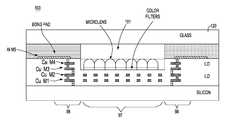
- FIG. 3illustrates, through a cross-sectional view, the CMOS image sensor chip 100 having a recessed dielectric according to a first embodiment of the invention.
- the CMOS imager array 100includes a recessed dielectric structure 101 in which is formed the array of color filters and corresponding microlens structures.
- the recess 101particularly protects lenses during the process of bonding the glass plate 120 to the CMOS sensor array chip.
- standard devices and wiringare fabricated, however, upper wiring layers are not formed over imager array 100 microlens structures.
- the array 10includes a plurality of metal wiring layers M 1 -M 5 interconnected by vias, for example, formed at dense wiring regions 98 of the peripheral circuits where at least five (M 1 -M 5 ) metallization levels are fabricated. This is compared to the active pixel region 97 formed between dense wiring regions 98 of the imager chip where only up to two metallization levels (M 1 -M 2 ) and interlevel dielectrics are formed. It is noted that conventional damascene or subtractive etch techniques may be used to form the metal structures and via structures that interconnect the metal level structures M 1 -M 5 in the dense wiring regions 98 .
- FIGS. 4A-4Edepict, through cross-sectional views, a process for fabricating the CMOS image sensor array structure 100 of FIG. 3 according to the invention.
- Standard processingyields the intermediate sensor stack structure 200 shown in FIG. 4A as now described.
- Cu metallization interconnects M 1 , M 2allowing for the formation of thinner stack of interlevel dielectric layers 130 a - 130 c formed on the substrate 15 .
- the substrate 14may be a bulk semiconductor including, for example, Si, SiGe, SiC, SiGeC, GaAs, InP, InAs and other III-V compound semiconductors, II-V compound semiconductors, or layered semiconductors such as silicon-on-insulators (SOI), SiC-on-insulator (SICOI) or silicon germanium-on-insulators (SGOI).
- SOIsilicon-on-insulators
- SICOISiC-on-insulator
- SGOIsilicon germanium-on-insulators
- the interlevel dielectric materialmay comprise an organic or inorganic interlevel dielectric (ILD) material which may be deposited by any of number of well known techniques such as sputtering, spin-on, or PECVD and may include a conventional spun-on organic dielectrics, spun-on inorganic dielectrics or combinations thereof which have a dielectric constant of about 4.2 or less.
- ILDorganic or inorganic interlevel dielectric
- Suitable organic dielectrics that can be employed in the present inventioninclude dielectrics that comprise C, O, F and/or H.
- organic dielectricsexamples include, but are not limited to: aromatic thermosetting polymeric resins, for example, resins sold by DOW Chemical Company under the tradename SiLK®, Honeywell under the tradename Flare®, and similar resins from other suppliers, and other like organic dielectrics.
- aromatic thermosetting polymeric resinsfor example, resins sold by DOW Chemical Company under the tradename SiLK®, Honeywell under the tradename Flare®, and similar resins from other suppliers, and other like organic dielectrics.
- the organic dielectric employed as interlevel dielectric layersmay or may not be porous, with porous organic dielectric layers being highly preferred due to the reduced k value.
- Suitable inorganic dielectrics that may be employed as the interlevel dielectrictypically comprise Si, O and H, and optionally C, e.g., SiO 2 , FSG (fluorosilicate glass), SiCOH, SiOCH, carbon-doped oxides (CDO), silicon-oxicarbides, organosilicate glasses (OSG) deposited by plasma enhanced chemical vapor deposition (CVD) techniques.
- Ce.g., SiO 2 , FSG (fluorosilicate glass), SiCOH, SiOCH, carbon-doped oxides (CDO), silicon-oxicarbides, organosilicate glasses (OSG) deposited by plasma enhanced chemical vapor deposition (CVD) techniques.
- Illustrative examples of some types of inorganic dielectricsinclude, but are not limited to: the silsesquioxane HOSP (sold by Honeywell), methylsilsesquioxane (MSQ), hydrogen silsesquioxane (HSQ), MSQ-HSQ copolymers, SiO 2 deposited using tetraethylorthosilicate (TEOS) or SiH 4 as a silicon source and O 2 , N 2 O, NO, etc. as an oxidizer; organosilanes and any other Si-containing material.
- the inorganic dielectric materialis SiO 2 .
- the methodology for forming the M 1 layerincludes first depositing the SiO 2 dielectric layer 130 c , e.g., to a thickness ranging between about 2 k ⁇ to 20 k ⁇ with a range of between 3 k ⁇ and 4 k ⁇ preferred, on top of the substrate which may include a capping layer (not shown), patterning trenches in the SiO 2 layer 130 c using known lithography and RIE techniques, and, lining the formed trenches with a metal liner such as one or more refractory metals, e.g., Ta, TaN, TiN, TiSiN, W, WCN, Ru.
- a metal linersuch as one or more refractory metals, e.g., Ta, TaN, TiN, TiSiN, W, WCN, Ru.
- the lined trenchesare filled with a copper material to form the Cu M 1 layer 135 b which is subsequently polished using known CMP technique.
- a barrier layer(not shown), such as SiN, may be deposited on top of the Cu M 1 metallization 135 b , e.g., to a thickness ranging between about 20 ⁇ to 2 k ⁇ with a range of between 100 ⁇ and 200 ⁇ preferred.
- the thickness of the nitride layer on top of the Cu interconnectis reduced to minimize reflectance.
- barrier layers materialsmay be used including, but not limited to, SiON, SiC, SiCN, SiCON, SiCO materials etc.
- a thin M 2 dielectric layer 130 be.g., SiO 2
- the M 2 metallization layeris formed by patterning trenches in the SiO 2 layer 130 b using known lithography and RIE techniques, lining the formed trenches with a metal liner such as a refractory metal, and, filling the lined trenches with a copper material to form the Cu M 2 135 a layer which is subsequently polished using known CMP technique.
- a barrier or Cu diffusion layer(not shown), such as SiN, may be deposited on top of the Cu M 2 layer 135 a , e.g., to a thickness ranging between about 20 ⁇ to 2 k ⁇ .
- the total thickness of both the M 1 and M 2 diffusion barriersbe about 20 nm or less, in order to minimize reflectance.
- an additional layer of materials with an index of refraction that is in between that of SiN (1.98) and SiO 2 (1.46), such as SiONcan be formed on top of the thin SiN barrier layers to comparable thicknesses (e.g., about 20 ⁇ to 2 k ⁇ ) to further reduce reflections.
- each pixel of array 100may include an additional STI isolation dielectric region formed in the substrate on top of the light sensitive element, e.g., photodiode.
- a bottom nitride capping layeris removed from the pixel optical path.
- those portions of the barrier SiN layers formed in the pixel array optical pathsare selectively removed to avoid the refraction index mismatch problem.
- an additional maska resist mask or a hardmask
- an additional lithography patterning and etching step(wet or dry etch) is implemented to open up the SiN at the select locations. It is understood however, that a maskless process may be implemented for removing select portions of the SiN layers, e.g., using clustered ion beam etching.
- a fluorine-based dry etche.g., CF 4 plus an oxygen plasma
- a wet etchis desirable to minimize damage or roughness at the surface after the etch (which might cause reflections or scattering of the light).
- the wet etchmay comprise of a dilute HF “smoothing” etch after SiN RE, or it could be an H 3 PO 4 etch to remove the SiN, using SiO 2 as a hardmask.
- process steps of forming the interlevel dielectric layer 130 c , the Cu M 1 metallization layer 135 b , and corresponding SiN barrier layer depositionis conducted, and selective removal of the barrier SiN layer in the pixel array optical path is performed.
- each of the M 3 and M 4 metallization layersinclude M 3 and M 4 conductive structures 140 , 145 , respectively, formed at the dense wiring logic regions 98 of the chip and are not formed over the M 1 and M 2 metallizations that reside at each pixel between the defined active pixel sensor optical paths of the imager array.
- the next stepinvolves the formation of fifth metallization level M 5 including a conductor 150 (e.g., an aluminum conductor) that may electrically couple any logic circuitry (not shown) with the package lead used to connect to an external circuit and/or chip.
- a conductor 150e.g., an aluminum conductor
- the conductive structure 150 of metallization level M 5is formed at the dense wiring logic regions 98 of the chip and are not formed directly over the M 1 and M 2 metallizations that reside between the defined active pixel sensor optical paths of the imager array region 97 .
- a passivation layer 160formed of one or more dielectric materials, such as SiO 2 , SiN, or polyimide on top of the last dielectric level 130 to insulate the conductors 150 of the M 5 metallization.
- This passivation layerwill be subsequently etched to form a pair of pads that form the structure used to bond a protective covering, e.g., a glass plate, on top of the array and are typically 0.5 microns to 50 microns in thickness.
- a protective coveringe.g., a glass plate
- FIG. 4Bthere is depicted through cross-sectional view, the resulting structure 200 ′ after the final M 5 metal level is processed, and a trench 101 is etched in the interlevel dielectric layer stack in the imager array region 97 using conventional lithography and RIE.
- Thismay be performed with an additional mask or, it can be part of a final via process. For instance, this may comprise steps depositing a passivation of last metal level M 5 , forming openings over bond pads and over the array, etching passivation over bond pads and at the same time forming the recess over the pixel array, and stripping the remaining resist.
- the passivation layer 160 and the interlevel dielectric layer 130are etched to form a trench or opening 101 having a width and length commensurate with the area of the image sensor pixel array to be formed, i.e., aligned with and disposed above the optical paths of a plurality of pixels and providing a surface upon which the color filters and microlens array are subsequently formed. It is seen from FIG. 4B that the sidewalls 102 a, b of the trench opening 101 are inset a small distance from the formed metallizations M 3 -M 4 and self-aligned with edges of the passivation layer 160 .
- This small insetdefines a peripheral region 98 where more dense logic circuitry is formed so as not to interfere with the active pixel cell array in region 97 .
- a photolithographic maskis subsequently patterned above the formed passivation layer 160 and developed and etched to open up the trench 101 corresponding in area spreading across a plurality of pixels in a subsequent single step etch process.
- a wet or dry etch processe.g., a F-based dry etch
- a wet or dry etch processas known in the art may be used to create the trench 101 by effectively removing a portion of the overlying bond pad layer and that portion of the interlevel dielectric layer 130 above the third ILD layer 130 a corresponding to metallization level M 2 in the manner as shown in FIG. 4B .
- FIG. 4BAs depicted in FIG.
- the ILD dielectricis etched to a predetermined depth above the surface of the third ILD layer 130 a .
- RIEetching
- standard parallel plate, downstream plasma, or high density plasma chamberscould be used with perfluorocarbon (PFC) and/or hydrofluorocarbon (HFC) gases used as a fluorine source and oxygen, hydrogen, nitrogen, argon, etc. used as dilutant gases, as known in the art.
- PFCperfluorocarbon
- HFChydrofluorocarbon
- dilute hydrofluoric acidcould be used to etch the ILD material (e.g., SiO 2 or similar oxide films); phosphoric acid could be used to etch SiN or similar films, etc. as known in the art.
- the opening 101 formed in the structure shown in FIG. 4B pixelmay be of the order of about 0.2 ⁇ m-4.0 ⁇ m deep, and of the order of about 1 mm-10 mm wide.
- the etched opening 101is shown in FIG. 4B to be substantially parallel but may be slightly tapered (e.g., having a wider top opening than bottom).
- an M 3 etch stop layer 171formed on top of the third ILD level 130 a extending substantially across the length of said pixel array region 97 .
- the etch stop layer 171provides mechanical protection for underlying layers and/or structures but additionally provides chemical and/or ion protection, among other things, for example.
- layer 171may also include one or more layers including materials such as, but not limited to: copper, aluminum, silicon nitride, silicon carbide, silicon oxynitride, silicon oxide, silicon dioxide, silicon carbonitride, organic polymers such as polyimide and/or other materials, for example.
- layer 171can be formed to a thickness of between about 20 to about 100 nanometers.
- the additional interlevel dielectric layer 130is formed above the etch stop layer 171 corresponding to metallization level M 3 which may include an oxide based material formed to between about 50 to about 500 nanometers, for example. Then, as depicted in FIG.
- an etch process(a wet or a dry etch such as RIE) of the ILD 130 layer is performed that stops at the etch stop layer 171 according to known techniques.
- the etch stop layer 171can be removed by conventional etch techniques as shown in FIG. 4 B( 2 ) resulting in the structure 200 ′ shown in FIG. 4 B( 2 ) having the recessed dielectric. If the etch stop is a dielectric such as SiN, it can be left in the stack to provide protection to the underlying wires.
- FIG. 4Cillustrates, through a cross-sectional view, the resulting structure after the recess etch and formation of color filters 125 and microlens array 122 arranged along the X- and Y-directions thereon to form a two-dimensional image sensor array over image area 97 by conventional processing.
- each pixel of the image sensorcomprises a color filter 125 of colorant material (e.g., RGB (primary color filters) or cyan, magenta and yellow filters (complementary color filters)), which, in one embodiment, may comprise a negative photoresist based on an acrylic polymer material including color pigments that is formed on the third ILD layer 130 a using known techniques.
- RGBprimary color filters
- cyan, magenta and yellow filterscompact color filters
- an over coat layermay be formed on the resulting color filter layer(s) 125 and on any exposed surfaces of the third interlevel dielectric dielectric film to planarize the topography associated with the color filters.
- This planarizing layeris typically an organic material, such as resist, with a thickness ranging from 0.2 ⁇ m to 2.0 ⁇ m.
- the microlens structures of the microlens array 122is then formed thereover by conventional techniques. Each microlens structure has a spherical surface and is regularly arranged along the X- and Y-directions to form a two-dimensional array in alignment with a color filter. Conventional techniques for forming the microlens structure 122 may be performed, e.g., forming a transparent insulating material, e.g., silicon-nitride, that is etched to form microlenses 122 .
- FIGS. 4E and 4FAn alternate process flow ( FIGS. 4E and 4F ) is as follows: After fabricating the final metal layer, M 5 , the dielectric is removed over the array using lithography and RIE. Then, one or more inorganic passivation layers 155 such as SiN or SiO 2 /SiN are deposited over the structure, which protects the underlying circuits from contamination. The total thickness of the inorganic dielectric ranges from 0.1 ⁇ m to 1 ⁇ m. Next, the color filters and microlenses are formed as shown in FIG. 4E . Finally, the polyimide spacers 160 are formed over the peripheral circuits, and the glass plate 120 is then attached to the polyimide 160 as shown in FIG. 4F .
- the inorganic passivation layers 155such as SiN or SiO 2 /SiN are deposited over the structure, which protects the underlying circuits from contamination. The total thickness of the inorganic dielectric ranges from 0.1 ⁇ m to 1 ⁇ m.
- FIG. 4Dthere is depicted the step of bonding a glass plate 120 to the previously formed (polyimide) passivation layers 160 using a bonding cement such as an acrylic adhesive with optimized optical performance and curing properties.
- a bonding cementsuch as an acrylic adhesive with optimized optical performance and curing properties.
- an air gap 190 of similar thickness as the bond pad structure 125is created between the microlens array 122 and the packaging glass.
- the height of the air gapranges from 2 ⁇ m up to 50 ⁇ m, to ensure that the defects on the surface of the glass do not touch the microlenses and that these defects are not imaged by the sensor.
- the recess 101is of such a depth that the formed lenses 125 are particularly protected during the process of bonding the glass plate 120 to the CMOS sensor array chip.
- the glass plate to be bondedmay range from between about 400 microns-600 microns in thickness.
- the additional step of packaging the formed image sensor devicethere is performed the additional step of packaging the formed image sensor device.
- FIG. 4Dthere depicts the step of forming openings in the glass plate 120 and passivation layer 160 , for example, by conventional etching processes that exposes the last metallization level, e.g., metallization level M 5 comprising the Aluminum bonding pad 150 .
- This forming of openings in glass plate for the wirebondingmay occur either before or after glass plate bonding as conventionally known.
- a conductor 199e.g. a bond wire
- the packaging of the image array having recessed dielectric portionmay comprise forming a Schott package configuration 300 utilizing semiconductor wafer packaging technique may involve forming silicon-via-contacts 305 that enable direct access to the contact- and/or test-pads from the backside of the substrate 15 .
- a photo resist mask applied to the backside of the siliconis used to define both, the position and size of the viaholes and the streets used to delineate dicing of the dies having respective formed image sensor arrays.
- the mask design as well as the thickness of the photo resistis optimized for the given silicon thickness.
- tapered side-walls structuresare etched in the underlying silicon substrate.
- the formed tapered via holesare etched by a highly customized plasma-etch process.
- the interdielectric layer underneath the contact pads in a second plasma-etching stepenables the direct electrical contact to the metallization pads, e.g., at the M 1 level.
- a sputter deposit of Ti:W/Cu material as an adhesion- and seed-layer for platingis performed.
- leads 310are formed that run up the tapered side-wall to the position of the corresponding contact pad of the formed metal contacts in the dense wiring region 98 of the imager array.
- the leads 310are electro-plated with copper to a predetermined thickness (e.g., about 5.5 ⁇ m).
- These leads 310may be electrically contacted with Ball Grid array contacts, e.g., solder balls 215 , and conventional under-bump-metallurgy (not shown) to complete the Schott package 300 for the imager array.
- Ball Grid array contactse.g., solder balls 215
- conventional under-bump-metallurgynot shown
- Schott packaging techniquethat can be used in accordance with the present invention for packaging the image sensor array with recessed dielectric can be found in the reference entitled “New Wafer-Level-Packaging Technology using Silicon-Via-Contacts For Optical And Other Sensor Applications” by Jürgen Leib, et al., in Electronic Components and Technology Conference, pp. 843-847 (2004), the whole contents and disclosure of which is incorporated by reference herein.
- the packaging of the image array having recessed dielectric portionmay comprise forming a Shellcase package configuration 400 utilizing semiconductor wafer level packaging techniques as known in the art.
- substrate material between diesis etched away yielding individual IC's attached to the supporting cover.
- the grooves formed between the diesare filled with an inert material and a thin cover is bonded onto the backside of the silicon dies to achieve a complete protective enclosure for each die.
- deep notchesare formed between the dies to expose the cross-section of the wire bond pads 150 .
- a metal layer 410is then formed so as to contact the metal pads at their cross sections.
- This metal layer 410may be patterned by a lithographic process to form individual leads, contacting the pads and forming solder pads on the upper surface of the package. The contacts may then be plated, e.g., with gold or lead-tin. Finally, wafer dicing is performed to yield the individual packaged dies. Further details regarding ShellCase packaging technique that can be used in accordance with the present invention for packaging the image sensor array with recessed dielectric can be found in the reference entitled “CSP Optoelectronic package for Imaging and Light Detection Applications” by I. Schweky, Proceedings of SPIE—The International Society for Optical Engineering Vol. 3582, pp. 876-881 (1998), the whole contents and disclosure of which is incorporated by reference herein.
Landscapes
- Solid State Image Pick-Up Elements (AREA)
- Transforming Light Signals Into Electric Signals (AREA)
Abstract
Description
Claims (11)
Priority Applications (4)
| Application Number | Priority Date | Filing Date | Title |
|---|---|---|---|
| US11/560,882US7781781B2 (en) | 2006-11-17 | 2006-11-17 | CMOS imager array with recessed dielectric |
| PCT/EP2007/061705WO2008058847A1 (en) | 2006-11-17 | 2007-10-30 | A cmos imager array with recessed dielectric layer |
| KR1020097009588AKR20090086550A (en) | 2006-11-17 | 2007-10-30 | CMOS Imager Array with Recessed Dielectric Layer |
| JP2009536692AJP5340950B2 (en) | 2006-11-17 | 2007-10-30 | CMOS imager array with recessed dielectric and method for manufacturing the same |
Applications Claiming Priority (1)
| Application Number | Priority Date | Filing Date | Title |
|---|---|---|---|
| US11/560,882US7781781B2 (en) | 2006-11-17 | 2006-11-17 | CMOS imager array with recessed dielectric |
Publications (2)
| Publication Number | Publication Date |
|---|---|
| US20080116537A1 US20080116537A1 (en) | 2008-05-22 |
| US7781781B2true US7781781B2 (en) | 2010-08-24 |
Family
ID=38877121
Family Applications (1)
| Application Number | Title | Priority Date | Filing Date |
|---|---|---|---|
| US11/560,882Active2028-11-20US7781781B2 (en) | 2006-11-17 | 2006-11-17 | CMOS imager array with recessed dielectric |
Country Status (4)
| Country | Link |
|---|---|
| US (1) | US7781781B2 (en) |
| JP (1) | JP5340950B2 (en) |
| KR (1) | KR20090086550A (en) |
| WO (1) | WO2008058847A1 (en) |
Cited By (31)
| Publication number | Priority date | Publication date | Assignee | Title |
|---|---|---|---|---|
| US20080116544A1 (en)* | 2006-11-22 | 2008-05-22 | Tessera, Inc. | Packaged semiconductor chips with array |
| US20090212381A1 (en)* | 2008-02-26 | 2009-08-27 | Tessera, Inc. | Wafer level packages for rear-face illuminated solid state image sensors |
| US20100019387A1 (en)* | 2008-07-23 | 2010-01-28 | Oki Semiconductor Co., Ltd. | Semiconductor device and fabrication method of the same |
| US20100213560A1 (en)* | 2009-02-24 | 2010-08-26 | Taiwan Semiconductor Manufacturing Company, Ltd. | Pad design for backside illuminated image sensor |
| US20100220226A1 (en)* | 2009-02-24 | 2010-09-02 | Taiwan Semiconductor Manufacturing Company, Ltd. | Front side implanted guard ring structure for backside illuminated image sensor |
| US20110274395A1 (en)* | 2010-05-06 | 2011-11-10 | Edris Mohammed M | Wafer integrated optical sub-modules |
| US20110309490A1 (en)* | 2010-06-18 | 2011-12-22 | Taiwan Semiconductor Manufacturing Company, Ltd. | Plasma Treatment for Semiconductor Devices |
| US8310036B2 (en) | 2007-03-05 | 2012-11-13 | DigitalOptics Corporation Europe Limited | Chips having rear contacts connected by through vias to front contacts |
| US20130020665A1 (en)* | 2011-07-19 | 2013-01-24 | Vage Oganesian | Low Stress Cavity Package For Back Side Illuminated Image Sensor, And Method Of Making Same |
| US8587126B2 (en) | 2010-12-02 | 2013-11-19 | Tessera, Inc. | Stacked microelectronic assembly with TSVs formed in stages with plural active chips |
| US8610259B2 (en) | 2010-09-17 | 2013-12-17 | Tessera, Inc. | Multi-function and shielded 3D interconnects |
| US8610264B2 (en) | 2010-12-08 | 2013-12-17 | Tessera, Inc. | Compliant interconnects in wafers |
| US8637968B2 (en) | 2010-12-02 | 2014-01-28 | Tessera, Inc. | Stacked microelectronic assembly having interposer connecting active chips |
| US8704347B2 (en) | 2006-11-22 | 2014-04-22 | Tessera, Inc. | Packaged semiconductor chips |
| US8736066B2 (en) | 2010-12-02 | 2014-05-27 | Tessera, Inc. | Stacked microelectronic assemby with TSVS formed in stages and carrier above chip |
| US8735287B2 (en) | 2007-07-31 | 2014-05-27 | Invensas Corp. | Semiconductor packaging process using through silicon vias |
| US8791575B2 (en) | 2010-07-23 | 2014-07-29 | Tessera, Inc. | Microelectronic elements having metallic pads overlying vias |
| US8796135B2 (en) | 2010-07-23 | 2014-08-05 | Tessera, Inc. | Microelectronic elements with rear contacts connected with via first or via middle structures |
| US20140264230A1 (en)* | 2013-03-14 | 2014-09-18 | Northrop Grumman Systems Corporation | Phase change material switch and method of making the same |
| US8847380B2 (en) | 2010-09-17 | 2014-09-30 | Tessera, Inc. | Staged via formation from both sides of chip |
| WO2015026040A1 (en)* | 2013-08-21 | 2015-02-26 | Dongbu Hitek Co., Ltd. | Method for manufacturing image sensor |
| US20150162632A1 (en)* | 2009-02-25 | 2015-06-11 | Bloom Energy Corporation | Fuel cell monitoring and control system |
| US20160187586A1 (en)* | 2014-12-29 | 2016-06-30 | Hon Hai Precision Industry Co., Ltd. | Optical fiber connector and optical coupling lens |
| US20170110641A1 (en)* | 2014-10-22 | 2017-04-20 | Xintec Inc. | Semiconductor package and manufacturing method thereof |
| US9640437B2 (en) | 2010-07-23 | 2017-05-02 | Tessera, Inc. | Methods of forming semiconductor elements using micro-abrasive particle stream |
| US9667900B2 (en) | 2013-12-09 | 2017-05-30 | Optiz, Inc. | Three dimensional system-on-chip image sensor package |
| US9683890B2 (en) | 2015-06-30 | 2017-06-20 | Semiconductor Components Industries, Llc | Image sensor pixels with conductive bias grids |
| US9972554B2 (en) | 2016-03-04 | 2018-05-15 | Powertech Technology Inc. | Wafer level chip scale package having continuous through hole via configuration and fabrication method thereof |
| US10325952B2 (en) | 2017-07-07 | 2019-06-18 | Advanced Semiconductor Engineering, Inc. | Semiconductor package device and method of manufacturing the same |
| US10700270B2 (en) | 2016-06-21 | 2020-06-30 | Northrop Grumman Systems Corporation | PCM switch and method of making the same |
| US11546010B2 (en) | 2021-02-16 | 2023-01-03 | Northrop Grumman Systems Corporation | Hybrid high-speed and high-performance switch system |
Families Citing this family (92)
| Publication number | Priority date | Publication date | Assignee | Title |
|---|---|---|---|---|
| US8029186B2 (en)* | 2004-11-05 | 2011-10-04 | International Business Machines Corporation | Method for thermal characterization under non-uniform heat load |
| KR100731128B1 (en)* | 2005-12-28 | 2007-06-22 | 동부일렉트로닉스 주식회사 | Manufacturing Method of CMOS Image Sensor |
| KR100731130B1 (en)* | 2005-12-29 | 2007-06-22 | 동부일렉트로닉스 주식회사 | CMOS image sensor and its manufacturing method |
| KR100660714B1 (en)* | 2005-12-29 | 2006-12-21 | 매그나칩 반도체 유한회사 | CMOS image sensor with backside illumination structure and manufacturing method thereof |
| US7675080B2 (en)* | 2006-01-10 | 2010-03-09 | Aptina Imaging Corp. | Uniform color filter arrays in a moat |
| KR100789578B1 (en)* | 2006-08-28 | 2007-12-28 | 동부일렉트로닉스 주식회사 | Image sensor and its manufacturing method |
| US8071416B2 (en)* | 2006-08-17 | 2011-12-06 | Micron Technology, Inc. | Method of forming a uniform color filter array |
| US20090090850A1 (en)* | 2006-08-31 | 2009-04-09 | Aptina Imaging Corporation | Deep Recess Color Filter Array and Process of Forming the Same |
| US7593248B2 (en)* | 2006-11-16 | 2009-09-22 | Aptina Imaging Corporation | Method, apparatus and system providing a one-time programmable memory device |
| US7875840B2 (en)* | 2006-11-16 | 2011-01-25 | Aptina Imaging Corporation | Imager device with anti-fuse pixels and recessed color filter array |
| US20070164196A1 (en)* | 2007-03-09 | 2007-07-19 | Tay Hiok N | Image sensor with pixel wiring to reflect light |
| KR100873275B1 (en)* | 2007-03-19 | 2008-12-11 | 매그나칩 반도체 유한회사 | Manufacturing Method of Image Sensor |
| JP2008270500A (en)* | 2007-04-19 | 2008-11-06 | Sharp Corp | Solid-state imaging device, manufacturing method thereof, and electronic information device |
| KR100866252B1 (en)* | 2007-05-17 | 2008-10-30 | 주식회사 동부하이텍 | Manufacturing Method of Image Sensor |
| JP5159192B2 (en)* | 2007-07-06 | 2013-03-06 | 株式会社東芝 | Manufacturing method of semiconductor device |
| KR100913326B1 (en)* | 2007-11-19 | 2009-08-20 | 주식회사 동부하이텍 | Image sensor and its manufacturing method |
| JP4799542B2 (en)* | 2007-12-27 | 2011-10-26 | 株式会社東芝 | Semiconductor package |
| KR100922929B1 (en)* | 2007-12-28 | 2009-10-22 | 주식회사 동부하이텍 | Image Sensor and Method for Manufacturing thereof |
| US8063465B2 (en) | 2008-02-08 | 2011-11-22 | Omnivision Technologies, Inc. | Backside illuminated imaging sensor with vertical pixel sensor |
| KR20100007257A (en)* | 2008-07-11 | 2010-01-22 | 삼성전자주식회사 | Image sensor and method for manufacturing the same |
| KR101010375B1 (en)* | 2008-08-06 | 2011-01-21 | 주식회사 동부하이텍 | Image sensor and manufacturing method |
| US9478685B2 (en) | 2014-06-23 | 2016-10-25 | Zena Technologies, Inc. | Vertical pillar structured infrared detector and fabrication method for the same |
| US8299472B2 (en)* | 2009-12-08 | 2012-10-30 | Young-June Yu | Active pixel sensor with nanowire structured photodetectors |
| US8791470B2 (en) | 2009-10-05 | 2014-07-29 | Zena Technologies, Inc. | Nano structured LEDs |
| US8384007B2 (en)* | 2009-10-07 | 2013-02-26 | Zena Technologies, Inc. | Nano wire based passive pixel image sensor |
| US9000353B2 (en) | 2010-06-22 | 2015-04-07 | President And Fellows Of Harvard College | Light absorption and filtering properties of vertically oriented semiconductor nano wires |
| US8835831B2 (en) | 2010-06-22 | 2014-09-16 | Zena Technologies, Inc. | Polarized light detecting device and fabrication methods of the same |
| US8890271B2 (en) | 2010-06-30 | 2014-11-18 | Zena Technologies, Inc. | Silicon nitride light pipes for image sensors |
| US8889455B2 (en) | 2009-12-08 | 2014-11-18 | Zena Technologies, Inc. | Manufacturing nanowire photo-detector grown on a back-side illuminated image sensor |
| US8507840B2 (en) | 2010-12-21 | 2013-08-13 | Zena Technologies, Inc. | Vertically structured passive pixel arrays and methods for fabricating the same |
| US8866065B2 (en) | 2010-12-13 | 2014-10-21 | Zena Technologies, Inc. | Nanowire arrays comprising fluorescent nanowires |
| US8274039B2 (en) | 2008-11-13 | 2012-09-25 | Zena Technologies, Inc. | Vertical waveguides with various functionality on integrated circuits |
| US8735797B2 (en) | 2009-12-08 | 2014-05-27 | Zena Technologies, Inc. | Nanowire photo-detector grown on a back-side illuminated image sensor |
| US9343490B2 (en) | 2013-08-09 | 2016-05-17 | Zena Technologies, Inc. | Nanowire structured color filter arrays and fabrication method of the same |
| US9082673B2 (en) | 2009-10-05 | 2015-07-14 | Zena Technologies, Inc. | Passivated upstanding nanostructures and methods of making the same |
| US8519379B2 (en) | 2009-12-08 | 2013-08-27 | Zena Technologies, Inc. | Nanowire structured photodiode with a surrounding epitaxially grown P or N layer |
| US20110115041A1 (en)* | 2009-11-19 | 2011-05-19 | Zena Technologies, Inc. | Nanowire core-shell light pipes |
| US9406709B2 (en) | 2010-06-22 | 2016-08-02 | President And Fellows Of Harvard College | Methods for fabricating and using nanowires |
| US8269985B2 (en) | 2009-05-26 | 2012-09-18 | Zena Technologies, Inc. | Determination of optimal diameters for nanowires |
| US9299866B2 (en) | 2010-12-30 | 2016-03-29 | Zena Technologies, Inc. | Nanowire array based solar energy harvesting device |
| US8748799B2 (en) | 2010-12-14 | 2014-06-10 | Zena Technologies, Inc. | Full color single pixel including doublet or quadruplet si nanowires for image sensors |
| US20100304061A1 (en)* | 2009-05-26 | 2010-12-02 | Zena Technologies, Inc. | Fabrication of high aspect ratio features in a glass layer by etching |
| US7646943B1 (en) | 2008-09-04 | 2010-01-12 | Zena Technologies, Inc. | Optical waveguides in image sensors |
| US9515218B2 (en) | 2008-09-04 | 2016-12-06 | Zena Technologies, Inc. | Vertical pillar structured photovoltaic devices with mirrors and optical claddings |
| US8229255B2 (en)* | 2008-09-04 | 2012-07-24 | Zena Technologies, Inc. | Optical waveguides in image sensors |
| US8546742B2 (en)* | 2009-06-04 | 2013-10-01 | Zena Technologies, Inc. | Array of nanowires in a single cavity with anti-reflective coating on substrate |
| DE102008049188A1 (en)* | 2008-09-26 | 2010-04-01 | Osram Opto Semiconductors Gmbh | Optoelectronic module with a carrier substrate and a plurality of radiation-emitting semiconductor components and method for its production |
| US8193555B2 (en) | 2009-02-11 | 2012-06-05 | Megica Corporation | Image and light sensor chip packages |
| JP5572979B2 (en)* | 2009-03-30 | 2014-08-20 | ソニー株式会社 | Manufacturing method of semiconductor device |
| US8278769B2 (en)* | 2009-07-02 | 2012-10-02 | Avago Technologies Wireless Ip (Singapore) Pte. Ltd. | Compound semiconductor device and connectors |
| US8330840B2 (en)* | 2009-08-06 | 2012-12-11 | Aptina Imaging Corporation | Image sensor with multilayer interference filters |
| US8208768B2 (en)* | 2009-10-26 | 2012-06-26 | United Microelectronics Corp. | Focusing member and optoelectronic device |
| TWI474066B (en)* | 2009-10-28 | 2015-02-21 | United Microelectronics Corp | Focusing member and optoelectronic device |
| CN102054815B (en)* | 2009-11-09 | 2014-02-05 | 联华电子股份有限公司 | Photoelectric components |
| US8247852B2 (en) | 2009-11-17 | 2012-08-21 | Omnivision Technologies, Inc. | Backside illuminated imaging sensor with reinforced pad structure |
| KR20110061677A (en)* | 2009-12-02 | 2011-06-10 | 삼성전자주식회사 | Image sensor and its manufacturing method. |
| US8139907B2 (en)* | 2009-12-29 | 2012-03-20 | United Microelectronics Corp. | Optoelectronic device and method of forming the same |
| JP5771898B2 (en)* | 2010-03-17 | 2015-09-02 | 株式会社ニコン | Image sensor and camera |
| US8624342B2 (en)* | 2010-11-05 | 2014-01-07 | Invensas Corporation | Rear-face illuminated solid state image sensors |
| US20120274811A1 (en)* | 2011-04-28 | 2012-11-01 | Dmitry Bakin | Imaging devices having arrays of image sensors and precision offset lenses |
| US20130010165A1 (en)* | 2011-07-05 | 2013-01-10 | United Microelectronics Corp. | Optical micro structure, method for fabricating the same and applications thereof |
| JP2013041878A (en)* | 2011-08-11 | 2013-02-28 | Sony Corp | Imaging apparatus and camera module |
| US8710615B2 (en)* | 2011-08-31 | 2014-04-29 | Infineon Technologies Ag | Semiconductor device with an amorphous semi-insulating layer, temperature sensor, and method of manufacturing a semiconductor device |
| US9299740B2 (en)* | 2012-05-31 | 2016-03-29 | Taiwan Semiconductor Manufacturing Company, Ltd. | Image sensor with low step height between back-side metal and pixel array |
| KR20140065282A (en)* | 2012-11-21 | 2014-05-29 | 삼성전자주식회사 | Semiconductor device comprising tsv(through silicon via), and semiconductor package comprising the same |
| EP2772939B1 (en)* | 2013-03-01 | 2016-10-19 | Ams Ag | Semiconductor device for detection of radiation and method of producing a semiconductor device for detection of radiation |
| US9391113B2 (en)* | 2014-01-17 | 2016-07-12 | Taiwan Semiconductor Manufacturing Co., Ltd. | Image-sensor device structure and method of manufacturing |
| KR20150092581A (en)* | 2014-02-05 | 2015-08-13 | 삼성전자주식회사 | Wiring structure and method of forming the same |
| US9929126B2 (en) | 2014-04-03 | 2018-03-27 | Taiwan Semiconductor Manufacturing Company, Ltd. | Packages with metal line crack prevention design |
| CN105097852A (en)* | 2014-05-07 | 2015-11-25 | 中芯国际集成电路制造(上海)有限公司 | Semiconductor device manufacturing method and semiconductor device |
| US20160017487A1 (en)* | 2014-07-15 | 2016-01-21 | Applied Materials, Inc. | Integrated pre-clean and deposition of low-damage layers |
| CN104157663A (en)* | 2014-08-27 | 2014-11-19 | 上海集成电路研发中心有限公司 | CMOS image pixel array capable of improving incident light efficiency |
| TWI550842B (en)* | 2015-04-09 | 2016-09-21 | 力晶科技股份有限公司 | Image sensor |
| US9853076B2 (en) | 2015-04-16 | 2017-12-26 | Taiwan Semiconductor Manufacturing Co., Ltd. | Stacked grid for more uniform optical input |
| US9991307B2 (en) | 2015-04-16 | 2018-06-05 | Taiwan Semiconductor Manufacturing Co., Ltd. | Stacked grid design for improved optical performance and isolation |
| US9570493B2 (en) | 2015-04-16 | 2017-02-14 | Taiwan Semiconductor Manufacturing Co., Ltd. | Dielectric grid bottom profile for light focusing |
| US10014333B2 (en)* | 2015-08-26 | 2018-07-03 | Semiconductor Components Industries, Llc | Back-side illuminated pixels with interconnect layers |
| US10833119B2 (en)* | 2015-10-26 | 2020-11-10 | Taiwan Semiconductor Manufacturing Co., Ltd. | Pad structure for front side illuminated image sensor |
| US9847359B2 (en) | 2015-11-17 | 2017-12-19 | Semiconductor Components Industries, Llc | Image sensors with improved surface planarity |
| US9996725B2 (en)* | 2016-11-03 | 2018-06-12 | Optiz, Inc. | Under screen sensor assembly |
| US10026818B1 (en) | 2017-01-19 | 2018-07-17 | Globalfoundries Inc. | Field effect transistor structure with recessed interlayer dielectric and method |
| TWI652806B (en)* | 2017-09-08 | 2019-03-01 | 奇景光電股份有限公司 | Flat panel display with fingerprint sensor embedded therein and method of forming same |
| TWI637225B (en)* | 2017-09-08 | 2018-10-01 | 奇景光電股份有限公司 | Flat panel display with fingerprint sensor embedded therein and method of forming same |
| US10861829B2 (en)* | 2017-12-26 | 2020-12-08 | Illumina, Inc. | Sensor system |
| US11031358B2 (en)* | 2018-03-01 | 2021-06-08 | Marvell Asia Pte, Ltd. | Overhang model for reducing passivation stress and method for producing the same |
| TWI712959B (en)* | 2018-09-19 | 2020-12-11 | 世界先進積體電路股份有限公司 | Optical sensor and method for forming the same |
| US10712500B2 (en)* | 2018-10-17 | 2020-07-14 | Taiwan Semiconductor Manufacturing Company Ltd. | Semiconductor device and manufacturing method of the same |
| CN113519057B (en) | 2018-10-26 | 2025-08-22 | 普赛昆腾公司 | Isolation of integrated waveguide detectors using back-end processing |
| US10915727B2 (en) | 2018-12-28 | 2021-02-09 | Vanguard International Semiconductor Corporation | Optical sensor and method for forming the same |
| US11276724B2 (en)* | 2019-06-27 | 2022-03-15 | Semiconductor Components Industries, Llc | Electrical interconnection of image sensor package |
| CN113764443B (en) | 2020-06-05 | 2024-01-02 | 联华电子股份有限公司 | Photosensitive element |
| JP2022014507A (en)* | 2020-07-07 | 2022-01-20 | ソニーセミコンダクタソリューションズ株式会社 | Semiconductor package and method for producing semiconductor package |
Citations (9)
| Publication number | Priority date | Publication date | Assignee | Title |
|---|---|---|---|---|
| US6274917B1 (en) | 1999-10-12 | 2001-08-14 | Taiwan Semiconductor Manufacturing Company | High efficiency color filter process for semiconductor array imaging devices |
| US6608679B1 (en) | 1998-12-21 | 2003-08-19 | Xerox Corporation | Spectrophotometric analysis of input light |
| US6611037B1 (en) | 2000-08-28 | 2003-08-26 | Micron Technology, Inc. | Multi-trench region for accumulation of photo-generated charge in a CMOS imager |
| US6818934B1 (en) | 2003-06-24 | 2004-11-16 | Omnivision International Holding Ltd | Image sensor having micro-lens array separated with trench structures and method of making |
| US20050002107A1 (en) | 2003-07-01 | 2005-01-06 | Hiroyuki Nemoto | Erecting resin lens array and method of manufacturing the same |
| US20050082480A1 (en) | 2003-08-26 | 2005-04-21 | Aegis Semiconductor, Inc. | Infrared camera system |
| US6930336B1 (en) | 2001-06-18 | 2005-08-16 | Foveon, Inc. | Vertical-color-filter detector group with trench isolation |
| US20060038254A1 (en) | 2004-08-23 | 2006-02-23 | Joohyun Jin | Trench isolation structure and method of formation |
| US7364933B2 (en)* | 2005-02-02 | 2008-04-29 | Samsung Electronics, Co., Ltd. | Image sensor and method for forming the same |
Family Cites Families (11)
| Publication number | Priority date | Publication date | Assignee | Title |
|---|---|---|---|---|
| JP2000150846A (en)* | 1998-11-12 | 2000-05-30 | Olympus Optical Co Ltd | Solid-state imaging device and method of manufacturing the same |
| IL133453A0 (en)* | 1999-12-10 | 2001-04-30 | Shellcase Ltd | Methods for producing packaged integrated circuit devices and packaged integrated circuit devices produced thereby |
| JP2001298175A (en)* | 2000-04-12 | 2001-10-26 | Toshiba Corp | Imaging system |
| FR2829876B1 (en)* | 2001-09-18 | 2004-07-02 | St Microelectronics Sa | PHOTOSENSITIVE CELL INCORPORATING A LIGHT GUIDE AND MATRIX COMPOSED OF SUCH CELLS |
| EP1367650A1 (en)* | 2002-05-27 | 2003-12-03 | STMicroelectronics S.A. | Electronic device comprising electronic circuits and a photosensitive zone, and method of fabricating such a device |
| JP2004071931A (en)* | 2002-08-08 | 2004-03-04 | Sony Corp | Solid-state imaging device and manufacturing method therefor |
| WO2005076360A1 (en)* | 2004-02-04 | 2005-08-18 | Koninklijke Philips Electronics N.V. | Opto-electronic semiconductor device, method of manufacturing same, and camera provided with such a device |
| US7342268B2 (en)* | 2004-12-23 | 2008-03-11 | International Business Machines Corporation | CMOS imager with Cu wiring and method of eliminating high reflectivity interfaces therefrom |
| FR2880732B1 (en)* | 2005-01-13 | 2007-04-06 | St Microelectronics Sa | IMAGE SENSOR |
| JP2006229206A (en)* | 2005-02-14 | 2006-08-31 | Samsung Electronics Co Ltd | Image sensor having improved sensitivity and method of manufacturing the same |
| KR100807214B1 (en)* | 2005-02-14 | 2008-03-03 | 삼성전자주식회사 | Image sensor with improved sensitivity and manufacturing method thereof |
- 2006
- 2006-11-17USUS11/560,882patent/US7781781B2/enactiveActive
- 2007
- 2007-10-30JPJP2009536692Apatent/JP5340950B2/ennot_activeExpired - Fee Related
- 2007-10-30WOPCT/EP2007/061705patent/WO2008058847A1/enactiveApplication Filing
- 2007-10-30KRKR1020097009588Apatent/KR20090086550A/ennot_activeCeased
Patent Citations (13)
| Publication number | Priority date | Publication date | Assignee | Title |
|---|---|---|---|---|
| US6608679B1 (en) | 1998-12-21 | 2003-08-19 | Xerox Corporation | Spectrophotometric analysis of input light |
| US6274917B1 (en) | 1999-10-12 | 2001-08-14 | Taiwan Semiconductor Manufacturing Company | High efficiency color filter process for semiconductor array imaging devices |
| US6611037B1 (en) | 2000-08-28 | 2003-08-26 | Micron Technology, Inc. | Multi-trench region for accumulation of photo-generated charge in a CMOS imager |
| US6930336B1 (en) | 2001-06-18 | 2005-08-16 | Foveon, Inc. | Vertical-color-filter detector group with trench isolation |
| US6818934B1 (en) | 2003-06-24 | 2004-11-16 | Omnivision International Holding Ltd | Image sensor having micro-lens array separated with trench structures and method of making |
| US20050017278A1 (en) | 2003-06-24 | 2005-01-27 | Katsumi Yamamoto | Image sensor having micro-lens array separated with trench structures and method of making |
| US20050048690A1 (en) | 2003-06-24 | 2005-03-03 | Katsumi Yamamoto | Image sensor having micro-lens array separated with trench structures and method of making |
| US6911684B2 (en) | 2003-06-24 | 2005-06-28 | Omnivision International Holding Ltd | Image sensor having micro-lens array separated with trench structures and method of making |
| US6933167B2 (en) | 2003-06-24 | 2005-08-23 | Omnivision International Holding Ltd | Image sensor having micro-lens array separated with trench structures and method of making |
| US20050002107A1 (en) | 2003-07-01 | 2005-01-06 | Hiroyuki Nemoto | Erecting resin lens array and method of manufacturing the same |
| US20050082480A1 (en) | 2003-08-26 | 2005-04-21 | Aegis Semiconductor, Inc. | Infrared camera system |
| US20060038254A1 (en) | 2004-08-23 | 2006-02-23 | Joohyun Jin | Trench isolation structure and method of formation |
| US7364933B2 (en)* | 2005-02-02 | 2008-04-29 | Samsung Electronics, Co., Ltd. | Image sensor and method for forming the same |
Cited By (65)
| Publication number | Priority date | Publication date | Assignee | Title |
|---|---|---|---|---|
| US8569876B2 (en) | 2006-11-22 | 2013-10-29 | Tessera, Inc. | Packaged semiconductor chips with array |
| US9070678B2 (en) | 2006-11-22 | 2015-06-30 | Tessera, Inc. | Packaged semiconductor chips with array |
| US20080116544A1 (en)* | 2006-11-22 | 2008-05-22 | Tessera, Inc. | Packaged semiconductor chips with array |
| US8704347B2 (en) | 2006-11-22 | 2014-04-22 | Tessera, Inc. | Packaged semiconductor chips |
| US8653644B2 (en) | 2006-11-22 | 2014-02-18 | Tessera, Inc. | Packaged semiconductor chips with array |
| US9548254B2 (en) | 2006-11-22 | 2017-01-17 | Tessera, Inc. | Packaged semiconductor chips with array |
| US8735205B2 (en) | 2007-03-05 | 2014-05-27 | Invensas Corporation | Chips having rear contacts connected by through vias to front contacts |
| US8310036B2 (en) | 2007-03-05 | 2012-11-13 | DigitalOptics Corporation Europe Limited | Chips having rear contacts connected by through vias to front contacts |
| US8405196B2 (en) | 2007-03-05 | 2013-03-26 | DigitalOptics Corporation Europe Limited | Chips having rear contacts connected by through vias to front contacts |
| US8735287B2 (en) | 2007-07-31 | 2014-05-27 | Invensas Corp. | Semiconductor packaging process using through silicon vias |
| US20090212381A1 (en)* | 2008-02-26 | 2009-08-27 | Tessera, Inc. | Wafer level packages for rear-face illuminated solid state image sensors |
| US8115267B2 (en)* | 2008-07-23 | 2012-02-14 | Lapis Semiconductor Co., Ltd. | Semiconductor device and fabrication method of the same |
| US20100019387A1 (en)* | 2008-07-23 | 2010-01-28 | Oki Semiconductor Co., Ltd. | Semiconductor device and fabrication method of the same |
| US9773828B2 (en) | 2009-02-24 | 2017-09-26 | Taiwan Semiconductor Manufacturing Co., Ltd. | Image sensor device and method of forming same |
| US10290671B2 (en) | 2009-02-24 | 2019-05-14 | Taiwan Semiconductor Manufacturing Co., Ltd. | Image sensor device and method of forming same |
| US9142586B2 (en)* | 2009-02-24 | 2015-09-22 | Taiwan Semiconductor Manufacturing Company, Ltd. | Pad design for backside illuminated image sensor |
| US8810700B2 (en) | 2009-02-24 | 2014-08-19 | Taiwan Semiconductor Manufacturing Company, Ltd. | Front side implanted guard ring structure for backside |
| US8531565B2 (en) | 2009-02-24 | 2013-09-10 | Taiwan Semiconductor Manufacturing Company, Ltd. | Front side implanted guard ring structure for backside illuminated image sensor |
| US20100220226A1 (en)* | 2009-02-24 | 2010-09-02 | Taiwan Semiconductor Manufacturing Company, Ltd. | Front side implanted guard ring structure for backside illuminated image sensor |
| US20100213560A1 (en)* | 2009-02-24 | 2010-08-26 | Taiwan Semiconductor Manufacturing Company, Ltd. | Pad design for backside illuminated image sensor |
| US10879297B2 (en) | 2009-02-24 | 2020-12-29 | Taiwan Semiconductor Manufacturing Co., Ltd. | Image sensor device and method of forming same |
| US20150162632A1 (en)* | 2009-02-25 | 2015-06-11 | Bloom Energy Corporation | Fuel cell monitoring and control system |
| US9190681B2 (en)* | 2009-02-25 | 2015-11-17 | Bloom Energy Corporation | Method of controlling a fuel cell system using impedance determination |
| US20110274395A1 (en)* | 2010-05-06 | 2011-11-10 | Edris Mohammed M | Wafer integrated optical sub-modules |
| US8532449B2 (en)* | 2010-05-06 | 2013-09-10 | Intel Corporation | Wafer integrated optical sub-modules |
| US20110309490A1 (en)* | 2010-06-18 | 2011-12-22 | Taiwan Semiconductor Manufacturing Company, Ltd. | Plasma Treatment for Semiconductor Devices |
| US20140131861A1 (en)* | 2010-06-18 | 2014-05-15 | Taiwan Semiconductor Manufacturing Company, Ltd. | Plasma Treatment for Semiconductor Devices |
| US9418955B2 (en)* | 2010-06-18 | 2016-08-16 | Taiwan Semiconductor Manufacturing Company, Ltd. | Plasma treatment for semiconductor devices |
| US8629053B2 (en)* | 2010-06-18 | 2014-01-14 | Taiwan Semiconductor Manufacturing Company, Ltd. | Plasma treatment for semiconductor devices |
| US8791575B2 (en) | 2010-07-23 | 2014-07-29 | Tessera, Inc. | Microelectronic elements having metallic pads overlying vias |
| US8796135B2 (en) | 2010-07-23 | 2014-08-05 | Tessera, Inc. | Microelectronic elements with rear contacts connected with via first or via middle structures |
| US9640437B2 (en) | 2010-07-23 | 2017-05-02 | Tessera, Inc. | Methods of forming semiconductor elements using micro-abrasive particle stream |
| US8847380B2 (en) | 2010-09-17 | 2014-09-30 | Tessera, Inc. | Staged via formation from both sides of chip |
| US8610259B2 (en) | 2010-09-17 | 2013-12-17 | Tessera, Inc. | Multi-function and shielded 3D interconnects |
| US10354942B2 (en) | 2010-09-17 | 2019-07-16 | Tessera, Inc. | Staged via formation from both sides of chip |
| US9362203B2 (en) | 2010-09-17 | 2016-06-07 | Tessera, Inc. | Staged via formation from both sides of chip |
| US8809190B2 (en) | 2010-09-17 | 2014-08-19 | Tessera, Inc. | Multi-function and shielded 3D interconnects |
| US9847277B2 (en) | 2010-09-17 | 2017-12-19 | Tessera, Inc. | Staged via formation from both sides of chip |
| US9355948B2 (en) | 2010-09-17 | 2016-05-31 | Tessera, Inc. | Multi-function and shielded 3D interconnects |
| US8736066B2 (en) | 2010-12-02 | 2014-05-27 | Tessera, Inc. | Stacked microelectronic assemby with TSVS formed in stages and carrier above chip |
| US9368476B2 (en) | 2010-12-02 | 2016-06-14 | Tessera, Inc. | Stacked microelectronic assembly with TSVs formed in stages with plural active chips |
| US9620437B2 (en) | 2010-12-02 | 2017-04-11 | Tessera, Inc. | Stacked microelectronic assembly with TSVS formed in stages and carrier above chip |
| US8637968B2 (en) | 2010-12-02 | 2014-01-28 | Tessera, Inc. | Stacked microelectronic assembly having interposer connecting active chips |
| US9269692B2 (en) | 2010-12-02 | 2016-02-23 | Tessera, Inc. | Stacked microelectronic assembly with TSVS formed in stages and carrier above chip |
| US9099296B2 (en) | 2010-12-02 | 2015-08-04 | Tessera, Inc. | Stacked microelectronic assembly with TSVS formed in stages with plural active chips |
| US8587126B2 (en) | 2010-12-02 | 2013-11-19 | Tessera, Inc. | Stacked microelectronic assembly with TSVs formed in stages with plural active chips |
| US9224649B2 (en) | 2010-12-08 | 2015-12-29 | Tessera, Inc. | Compliant interconnects in wafers |
| US8796828B2 (en) | 2010-12-08 | 2014-08-05 | Tessera, Inc. | Compliant interconnects in wafers |
| US8610264B2 (en) | 2010-12-08 | 2013-12-17 | Tessera, Inc. | Compliant interconnects in wafers |
| US20130020665A1 (en)* | 2011-07-19 | 2013-01-24 | Vage Oganesian | Low Stress Cavity Package For Back Side Illuminated Image Sensor, And Method Of Making Same |
| US20140065755A1 (en)* | 2011-07-19 | 2014-03-06 | Optiz, Inc. | Method Of Making A Low Stress Cavity Package For Back Side Illuminated Image Sensor |
| US8895344B2 (en)* | 2011-07-19 | 2014-11-25 | Optiz, Inc. | Method of making a low stress cavity package for back side illuminated image sensor |
| US8604576B2 (en)* | 2011-07-19 | 2013-12-10 | Opitz, Inc. | Low stress cavity package for back side illuminated image sensor, and method of making same |
| US9257647B2 (en)* | 2013-03-14 | 2016-02-09 | Northrop Grumman Systems Corporation | Phase change material switch and method of making the same |
| US20140264230A1 (en)* | 2013-03-14 | 2014-09-18 | Northrop Grumman Systems Corporation | Phase change material switch and method of making the same |
| WO2015026040A1 (en)* | 2013-08-21 | 2015-02-26 | Dongbu Hitek Co., Ltd. | Method for manufacturing image sensor |
| US9667900B2 (en) | 2013-12-09 | 2017-05-30 | Optiz, Inc. | Three dimensional system-on-chip image sensor package |
| US20170110641A1 (en)* | 2014-10-22 | 2017-04-20 | Xintec Inc. | Semiconductor package and manufacturing method thereof |
| US9690060B2 (en)* | 2014-12-29 | 2017-06-27 | Hon Hai Precision Industry Co., Ltd. | Optical fiber connector and optical coupling lens |
| US20160187586A1 (en)* | 2014-12-29 | 2016-06-30 | Hon Hai Precision Industry Co., Ltd. | Optical fiber connector and optical coupling lens |
| US9683890B2 (en) | 2015-06-30 | 2017-06-20 | Semiconductor Components Industries, Llc | Image sensor pixels with conductive bias grids |
| US9972554B2 (en) | 2016-03-04 | 2018-05-15 | Powertech Technology Inc. | Wafer level chip scale package having continuous through hole via configuration and fabrication method thereof |
| US10700270B2 (en) | 2016-06-21 | 2020-06-30 | Northrop Grumman Systems Corporation | PCM switch and method of making the same |
| US10325952B2 (en) | 2017-07-07 | 2019-06-18 | Advanced Semiconductor Engineering, Inc. | Semiconductor package device and method of manufacturing the same |
| US11546010B2 (en) | 2021-02-16 | 2023-01-03 | Northrop Grumman Systems Corporation | Hybrid high-speed and high-performance switch system |
Also Published As
| Publication number | Publication date |
|---|---|
| WO2008058847A1 (en) | 2008-05-22 |
| KR20090086550A (en) | 2009-08-13 |
| JP2010510646A (en) | 2010-04-02 |
| US20080116537A1 (en) | 2008-05-22 |
| JP5340950B2 (en) | 2013-11-13 |
Similar Documents
| Publication | Publication Date | Title |
|---|---|---|
| US7781781B2 (en) | CMOS imager array with recessed dielectric | |
| US7772028B2 (en) | CMOS imager with Cu wiring and method of eliminating high reflectivity interfaces therefrom | |
| KR100992031B1 (en) | Damascene copper wiring image sensor | |
| US11456263B2 (en) | Semiconductor structure and method for forming the same | |
| US11296252B2 (en) | Method and apparatus for CMOS sensor packaging | |
| US8003425B2 (en) | Methods for forming anti-reflection structures for CMOS image sensors | |
| US7759755B2 (en) | Anti-reflection structures for CMOS image sensors | |
| US20190305026A1 (en) | Front side illuminated image sensor device structure and method for forming the same | |
| US20230387172A1 (en) | Anchor Structures And Methods For Uniform Wafer Planarization And Bonding | |
| US12009323B2 (en) | Semiconductor structure |
Legal Events
| Date | Code | Title | Description |
|---|---|---|---|
| AS | Assignment | Owner name:INTERNATIONAL BUSINESS MACHINES CORPORATION, NEW Y Free format text:ASSIGNMENT OF ASSIGNORS INTEREST;ASSIGNORS:ADKISSON, JAMES W.;GAMBINO, JEFFREY P.;HE, ZHONG-XIANG;AND OTHERS;REEL/FRAME:018530/0741;SIGNING DATES FROM 20061103 TO 20061115 Owner name:INTERNATIONAL BUSINESS MACHINES CORPORATION, NEW Y Free format text:ASSIGNMENT OF ASSIGNORS INTEREST;ASSIGNORS:ADKISSON, JAMES W.;GAMBINO, JEFFREY P.;HE, ZHONG-XIANG;AND OTHERS;SIGNING DATES FROM 20061103 TO 20061115;REEL/FRAME:018530/0741 | |
| FEPP | Fee payment procedure | Free format text:PAYOR NUMBER ASSIGNED (ORIGINAL EVENT CODE: ASPN); ENTITY STATUS OF PATENT OWNER: LARGE ENTITY | |
| STCF | Information on status: patent grant | Free format text:PATENTED CASE | |
| REMI | Maintenance fee reminder mailed | ||
| FPAY | Fee payment | Year of fee payment:4 | |
| SULP | Surcharge for late payment | ||
| AS | Assignment | Owner name:GLOBALFOUNDRIES U.S. 2 LLC, NEW YORK Free format text:ASSIGNMENT OF ASSIGNORS INTEREST;ASSIGNOR:INTERNATIONAL BUSINESS MACHINES CORPORATION;REEL/FRAME:036550/0001 Effective date:20150629 | |
| AS | Assignment | Owner name:GLOBALFOUNDRIES INC., CAYMAN ISLANDS Free format text:ASSIGNMENT OF ASSIGNORS INTEREST;ASSIGNORS:GLOBALFOUNDRIES U.S. 2 LLC;GLOBALFOUNDRIES U.S. INC.;REEL/FRAME:036779/0001 Effective date:20150910 | |
| MAFP | Maintenance fee payment | Free format text:PAYMENT OF MAINTENANCE FEE, 8TH YEAR, LARGE ENTITY (ORIGINAL EVENT CODE: M1552) Year of fee payment:8 | |
| AS | Assignment | Owner name:WILMINGTON TRUST, NATIONAL ASSOCIATION, DELAWARE Free format text:SECURITY AGREEMENT;ASSIGNOR:GLOBALFOUNDRIES INC.;REEL/FRAME:049490/0001 Effective date:20181127 | |
| AS | Assignment | Owner name:GLOBALFOUNDRIES U.S. INC., CALIFORNIA Free format text:ASSIGNMENT OF ASSIGNORS INTEREST;ASSIGNOR:GLOBALFOUNDRIES INC.;REEL/FRAME:054633/0001 Effective date:20201022 | |
| AS | Assignment | Owner name:GLOBALFOUNDRIES INC., CAYMAN ISLANDS Free format text:RELEASE BY SECURED PARTY;ASSIGNOR:WILMINGTON TRUST, NATIONAL ASSOCIATION;REEL/FRAME:054636/0001 Effective date:20201117 | |
| AS | Assignment | Owner name:GLOBALFOUNDRIES U.S. INC., NEW YORK Free format text:RELEASE BY SECURED PARTY;ASSIGNOR:WILMINGTON TRUST, NATIONAL ASSOCIATION;REEL/FRAME:056987/0001 Effective date:20201117 | |
| MAFP | Maintenance fee payment | Free format text:PAYMENT OF MAINTENANCE FEE, 12TH YEAR, LARGE ENTITY (ORIGINAL EVENT CODE: M1553); ENTITY STATUS OF PATENT OWNER: LARGE ENTITY Year of fee payment:12 |