US7781266B2 - Methods and apparatus for improved thermal performance and electromagnetic interference (EMI) shielding in leadframe integrated circuit (IC) packages - Google Patents
Methods and apparatus for improved thermal performance and electromagnetic interference (EMI) shielding in leadframe integrated circuit (IC) packagesDownload PDFInfo
- Publication number
- US7781266B2 US7781266B2US12/535,548US53554809AUS7781266B2US 7781266 B2US7781266 B2US 7781266B2US 53554809 AUS53554809 AUS 53554809AUS 7781266 B2US7781266 B2US 7781266B2
- Authority
- US
- United States
- Prior art keywords
- leadframe
- cap
- die
- package
- leads
- Prior art date
- Legal status (The legal status is an assumption and is not a legal conclusion. Google has not performed a legal analysis and makes no representation as to the accuracy of the status listed.)
- Expired - Fee Related
Links
Images


Classifications
- H—ELECTRICITY
- H01—ELECTRIC ELEMENTS
- H01L—SEMICONDUCTOR DEVICES NOT COVERED BY CLASS H10
- H01L23/00—Details of semiconductor or other solid state devices
- H01L23/34—Arrangements for cooling, heating, ventilating or temperature compensation ; Temperature sensing arrangements
- H01L23/42—Fillings or auxiliary members in containers or encapsulations selected or arranged to facilitate heating or cooling
- H01L23/433—Auxiliary members in containers characterised by their shape, e.g. pistons
- H01L23/4334—Auxiliary members in encapsulations
- H—ELECTRICITY
- H01—ELECTRIC ELEMENTS
- H01L—SEMICONDUCTOR DEVICES NOT COVERED BY CLASS H10
- H01L23/00—Details of semiconductor or other solid state devices
- H01L23/28—Encapsulations, e.g. encapsulating layers, coatings, e.g. for protection
- H01L23/31—Encapsulations, e.g. encapsulating layers, coatings, e.g. for protection characterised by the arrangement or shape
- H01L23/3107—Encapsulations, e.g. encapsulating layers, coatings, e.g. for protection characterised by the arrangement or shape the device being completely enclosed
- H01L23/3121—Encapsulations, e.g. encapsulating layers, coatings, e.g. for protection characterised by the arrangement or shape the device being completely enclosed a substrate forming part of the encapsulation
- H01L23/3128—Encapsulations, e.g. encapsulating layers, coatings, e.g. for protection characterised by the arrangement or shape the device being completely enclosed a substrate forming part of the encapsulation the substrate having spherical bumps for external connection
- H—ELECTRICITY
- H01—ELECTRIC ELEMENTS
- H01L—SEMICONDUCTOR DEVICES NOT COVERED BY CLASS H10
- H01L23/00—Details of semiconductor or other solid state devices
- H01L23/34—Arrangements for cooling, heating, ventilating or temperature compensation ; Temperature sensing arrangements
- H01L23/36—Selection of materials, or shaping, to facilitate cooling or heating, e.g. heatsinks
- H01L23/367—Cooling facilitated by shape of device
- H01L23/3677—Wire-like or pin-like cooling fins or heat sinks
- H—ELECTRICITY
- H01—ELECTRIC ELEMENTS
- H01L—SEMICONDUCTOR DEVICES NOT COVERED BY CLASS H10
- H01L23/00—Details of semiconductor or other solid state devices
- H01L23/48—Arrangements for conducting electric current to or from the solid state body in operation, e.g. leads, terminal arrangements ; Selection of materials therefor
- H01L23/488—Arrangements for conducting electric current to or from the solid state body in operation, e.g. leads, terminal arrangements ; Selection of materials therefor consisting of soldered or bonded constructions
- H01L23/495—Lead-frames or other flat leads
- H01L23/49541—Geometry of the lead-frame
- H—ELECTRICITY
- H01—ELECTRIC ELEMENTS
- H01L—SEMICONDUCTOR DEVICES NOT COVERED BY CLASS H10
- H01L23/00—Details of semiconductor or other solid state devices
- H01L23/48—Arrangements for conducting electric current to or from the solid state body in operation, e.g. leads, terminal arrangements ; Selection of materials therefor
- H01L23/488—Arrangements for conducting electric current to or from the solid state body in operation, e.g. leads, terminal arrangements ; Selection of materials therefor consisting of soldered or bonded constructions
- H01L23/495—Lead-frames or other flat leads
- H01L23/49568—Lead-frames or other flat leads specifically adapted to facilitate heat dissipation
- H—ELECTRICITY
- H01—ELECTRIC ELEMENTS
- H01L—SEMICONDUCTOR DEVICES NOT COVERED BY CLASS H10
- H01L23/00—Details of semiconductor or other solid state devices
- H01L23/552—Protection against radiation, e.g. light or electromagnetic waves
- H—ELECTRICITY
- H01—ELECTRIC ELEMENTS
- H01L—SEMICONDUCTOR DEVICES NOT COVERED BY CLASS H10
- H01L24/00—Arrangements for connecting or disconnecting semiconductor or solid-state bodies; Methods or apparatus related thereto
- H01L24/01—Means for bonding being attached to, or being formed on, the surface to be connected, e.g. chip-to-package, die-attach, "first-level" interconnects; Manufacturing methods related thereto
- H01L24/42—Wire connectors; Manufacturing methods related thereto
- H01L24/47—Structure, shape, material or disposition of the wire connectors after the connecting process
- H01L24/49—Structure, shape, material or disposition of the wire connectors after the connecting process of a plurality of wire connectors
- H—ELECTRICITY
- H01—ELECTRIC ELEMENTS
- H01L—SEMICONDUCTOR DEVICES NOT COVERED BY CLASS H10
- H01L24/00—Arrangements for connecting or disconnecting semiconductor or solid-state bodies; Methods or apparatus related thereto
- H01L24/93—Batch processes
- H01L24/95—Batch processes at chip-level, i.e. with connecting carried out on a plurality of singulated devices, i.e. on diced chips
- H01L24/97—Batch processes at chip-level, i.e. with connecting carried out on a plurality of singulated devices, i.e. on diced chips the devices being connected to a common substrate, e.g. interposer, said common substrate being separable into individual assemblies after connecting
- H—ELECTRICITY
- H01—ELECTRIC ELEMENTS
- H01L—SEMICONDUCTOR DEVICES NOT COVERED BY CLASS H10
- H01L2224/00—Indexing scheme for arrangements for connecting or disconnecting semiconductor or solid-state bodies and methods related thereto as covered by H01L24/00
- H01L2224/01—Means for bonding being attached to, or being formed on, the surface to be connected, e.g. chip-to-package, die-attach, "first-level" interconnects; Manufacturing methods related thereto
- H01L2224/26—Layer connectors, e.g. plate connectors, solder or adhesive layers; Manufacturing methods related thereto
- H01L2224/31—Structure, shape, material or disposition of the layer connectors after the connecting process
- H01L2224/32—Structure, shape, material or disposition of the layer connectors after the connecting process of an individual layer connector
- H01L2224/321—Disposition
- H01L2224/32151—Disposition the layer connector connecting between a semiconductor or solid-state body and an item not being a semiconductor or solid-state body, e.g. chip-to-substrate, chip-to-passive
- H01L2224/32221—Disposition the layer connector connecting between a semiconductor or solid-state body and an item not being a semiconductor or solid-state body, e.g. chip-to-substrate, chip-to-passive the body and the item being stacked
- H01L2224/32225—Disposition the layer connector connecting between a semiconductor or solid-state body and an item not being a semiconductor or solid-state body, e.g. chip-to-substrate, chip-to-passive the body and the item being stacked the item being non-metallic, e.g. insulating substrate with or without metallisation
- H—ELECTRICITY
- H01—ELECTRIC ELEMENTS
- H01L—SEMICONDUCTOR DEVICES NOT COVERED BY CLASS H10
- H01L2224/00—Indexing scheme for arrangements for connecting or disconnecting semiconductor or solid-state bodies and methods related thereto as covered by H01L24/00
- H01L2224/01—Means for bonding being attached to, or being formed on, the surface to be connected, e.g. chip-to-package, die-attach, "first-level" interconnects; Manufacturing methods related thereto
- H01L2224/26—Layer connectors, e.g. plate connectors, solder or adhesive layers; Manufacturing methods related thereto
- H01L2224/31—Structure, shape, material or disposition of the layer connectors after the connecting process
- H01L2224/32—Structure, shape, material or disposition of the layer connectors after the connecting process of an individual layer connector
- H01L2224/321—Disposition
- H01L2224/32151—Disposition the layer connector connecting between a semiconductor or solid-state body and an item not being a semiconductor or solid-state body, e.g. chip-to-substrate, chip-to-passive
- H01L2224/32221—Disposition the layer connector connecting between a semiconductor or solid-state body and an item not being a semiconductor or solid-state body, e.g. chip-to-substrate, chip-to-passive the body and the item being stacked
- H01L2224/32245—Disposition the layer connector connecting between a semiconductor or solid-state body and an item not being a semiconductor or solid-state body, e.g. chip-to-substrate, chip-to-passive the body and the item being stacked the item being metallic
- H—ELECTRICITY
- H01—ELECTRIC ELEMENTS
- H01L—SEMICONDUCTOR DEVICES NOT COVERED BY CLASS H10
- H01L2224/00—Indexing scheme for arrangements for connecting or disconnecting semiconductor or solid-state bodies and methods related thereto as covered by H01L24/00
- H01L2224/01—Means for bonding being attached to, or being formed on, the surface to be connected, e.g. chip-to-package, die-attach, "first-level" interconnects; Manufacturing methods related thereto
- H01L2224/42—Wire connectors; Manufacturing methods related thereto
- H01L2224/47—Structure, shape, material or disposition of the wire connectors after the connecting process
- H01L2224/48—Structure, shape, material or disposition of the wire connectors after the connecting process of an individual wire connector
- H01L2224/4805—Shape
- H01L2224/4809—Loop shape
- H01L2224/48091—Arched
- H—ELECTRICITY
- H01—ELECTRIC ELEMENTS
- H01L—SEMICONDUCTOR DEVICES NOT COVERED BY CLASS H10
- H01L2224/00—Indexing scheme for arrangements for connecting or disconnecting semiconductor or solid-state bodies and methods related thereto as covered by H01L24/00
- H01L2224/01—Means for bonding being attached to, or being formed on, the surface to be connected, e.g. chip-to-package, die-attach, "first-level" interconnects; Manufacturing methods related thereto
- H01L2224/42—Wire connectors; Manufacturing methods related thereto
- H01L2224/47—Structure, shape, material or disposition of the wire connectors after the connecting process
- H01L2224/48—Structure, shape, material or disposition of the wire connectors after the connecting process of an individual wire connector
- H01L2224/481—Disposition
- H01L2224/48151—Connecting between a semiconductor or solid-state body and an item not being a semiconductor or solid-state body, e.g. chip-to-substrate, chip-to-passive
- H01L2224/48221—Connecting between a semiconductor or solid-state body and an item not being a semiconductor or solid-state body, e.g. chip-to-substrate, chip-to-passive the body and the item being stacked
- H01L2224/48225—Connecting between a semiconductor or solid-state body and an item not being a semiconductor or solid-state body, e.g. chip-to-substrate, chip-to-passive the body and the item being stacked the item being non-metallic, e.g. insulating substrate with or without metallisation
- H01L2224/48227—Connecting between a semiconductor or solid-state body and an item not being a semiconductor or solid-state body, e.g. chip-to-substrate, chip-to-passive the body and the item being stacked the item being non-metallic, e.g. insulating substrate with or without metallisation connecting the wire to a bond pad of the item
- H01L2224/48228—Connecting between a semiconductor or solid-state body and an item not being a semiconductor or solid-state body, e.g. chip-to-substrate, chip-to-passive the body and the item being stacked the item being non-metallic, e.g. insulating substrate with or without metallisation connecting the wire to a bond pad of the item the bond pad being disposed in a recess of the surface of the item
- H—ELECTRICITY
- H01—ELECTRIC ELEMENTS
- H01L—SEMICONDUCTOR DEVICES NOT COVERED BY CLASS H10
- H01L2224/00—Indexing scheme for arrangements for connecting or disconnecting semiconductor or solid-state bodies and methods related thereto as covered by H01L24/00
- H01L2224/01—Means for bonding being attached to, or being formed on, the surface to be connected, e.g. chip-to-package, die-attach, "first-level" interconnects; Manufacturing methods related thereto
- H01L2224/42—Wire connectors; Manufacturing methods related thereto
- H01L2224/47—Structure, shape, material or disposition of the wire connectors after the connecting process
- H01L2224/48—Structure, shape, material or disposition of the wire connectors after the connecting process of an individual wire connector
- H01L2224/481—Disposition
- H01L2224/48151—Connecting between a semiconductor or solid-state body and an item not being a semiconductor or solid-state body, e.g. chip-to-substrate, chip-to-passive
- H01L2224/48221—Connecting between a semiconductor or solid-state body and an item not being a semiconductor or solid-state body, e.g. chip-to-substrate, chip-to-passive the body and the item being stacked
- H01L2224/48225—Connecting between a semiconductor or solid-state body and an item not being a semiconductor or solid-state body, e.g. chip-to-substrate, chip-to-passive the body and the item being stacked the item being non-metallic, e.g. insulating substrate with or without metallisation
- H01L2224/48237—Connecting between a semiconductor or solid-state body and an item not being a semiconductor or solid-state body, e.g. chip-to-substrate, chip-to-passive the body and the item being stacked the item being non-metallic, e.g. insulating substrate with or without metallisation connecting the wire to a die pad of the item
- H—ELECTRICITY
- H01—ELECTRIC ELEMENTS
- H01L—SEMICONDUCTOR DEVICES NOT COVERED BY CLASS H10
- H01L2224/00—Indexing scheme for arrangements for connecting or disconnecting semiconductor or solid-state bodies and methods related thereto as covered by H01L24/00
- H01L2224/01—Means for bonding being attached to, or being formed on, the surface to be connected, e.g. chip-to-package, die-attach, "first-level" interconnects; Manufacturing methods related thereto
- H01L2224/42—Wire connectors; Manufacturing methods related thereto
- H01L2224/47—Structure, shape, material or disposition of the wire connectors after the connecting process
- H01L2224/48—Structure, shape, material or disposition of the wire connectors after the connecting process of an individual wire connector
- H01L2224/481—Disposition
- H01L2224/48151—Connecting between a semiconductor or solid-state body and an item not being a semiconductor or solid-state body, e.g. chip-to-substrate, chip-to-passive
- H01L2224/48221—Connecting between a semiconductor or solid-state body and an item not being a semiconductor or solid-state body, e.g. chip-to-substrate, chip-to-passive the body and the item being stacked
- H01L2224/48245—Connecting between a semiconductor or solid-state body and an item not being a semiconductor or solid-state body, e.g. chip-to-substrate, chip-to-passive the body and the item being stacked the item being metallic
- H01L2224/48247—Connecting between a semiconductor or solid-state body and an item not being a semiconductor or solid-state body, e.g. chip-to-substrate, chip-to-passive the body and the item being stacked the item being metallic connecting the wire to a bond pad of the item
- H—ELECTRICITY
- H01—ELECTRIC ELEMENTS
- H01L—SEMICONDUCTOR DEVICES NOT COVERED BY CLASS H10
- H01L2224/00—Indexing scheme for arrangements for connecting or disconnecting semiconductor or solid-state bodies and methods related thereto as covered by H01L24/00
- H01L2224/01—Means for bonding being attached to, or being formed on, the surface to be connected, e.g. chip-to-package, die-attach, "first-level" interconnects; Manufacturing methods related thereto
- H01L2224/42—Wire connectors; Manufacturing methods related thereto
- H01L2224/47—Structure, shape, material or disposition of the wire connectors after the connecting process
- H01L2224/48—Structure, shape, material or disposition of the wire connectors after the connecting process of an individual wire connector
- H01L2224/481—Disposition
- H01L2224/48151—Connecting between a semiconductor or solid-state body and an item not being a semiconductor or solid-state body, e.g. chip-to-substrate, chip-to-passive
- H01L2224/48221—Connecting between a semiconductor or solid-state body and an item not being a semiconductor or solid-state body, e.g. chip-to-substrate, chip-to-passive the body and the item being stacked
- H01L2224/48245—Connecting between a semiconductor or solid-state body and an item not being a semiconductor or solid-state body, e.g. chip-to-substrate, chip-to-passive the body and the item being stacked the item being metallic
- H01L2224/48257—Connecting between a semiconductor or solid-state body and an item not being a semiconductor or solid-state body, e.g. chip-to-substrate, chip-to-passive the body and the item being stacked the item being metallic connecting the wire to a die pad of the item
- H—ELECTRICITY
- H01—ELECTRIC ELEMENTS
- H01L—SEMICONDUCTOR DEVICES NOT COVERED BY CLASS H10
- H01L2224/00—Indexing scheme for arrangements for connecting or disconnecting semiconductor or solid-state bodies and methods related thereto as covered by H01L24/00
- H01L2224/01—Means for bonding being attached to, or being formed on, the surface to be connected, e.g. chip-to-package, die-attach, "first-level" interconnects; Manufacturing methods related thereto
- H01L2224/42—Wire connectors; Manufacturing methods related thereto
- H01L2224/47—Structure, shape, material or disposition of the wire connectors after the connecting process
- H01L2224/48—Structure, shape, material or disposition of the wire connectors after the connecting process of an individual wire connector
- H01L2224/484—Connecting portions
- H01L2224/48463—Connecting portions the connecting portion on the bonding area of the semiconductor or solid-state body being a ball bond
- H01L2224/48465—Connecting portions the connecting portion on the bonding area of the semiconductor or solid-state body being a ball bond the other connecting portion not on the bonding area being a wedge bond, i.e. ball-to-wedge, regular stitch
- H—ELECTRICITY
- H01—ELECTRIC ELEMENTS
- H01L—SEMICONDUCTOR DEVICES NOT COVERED BY CLASS H10
- H01L2224/00—Indexing scheme for arrangements for connecting or disconnecting semiconductor or solid-state bodies and methods related thereto as covered by H01L24/00
- H01L2224/01—Means for bonding being attached to, or being formed on, the surface to be connected, e.g. chip-to-package, die-attach, "first-level" interconnects; Manufacturing methods related thereto
- H01L2224/42—Wire connectors; Manufacturing methods related thereto
- H01L2224/47—Structure, shape, material or disposition of the wire connectors after the connecting process
- H01L2224/49—Structure, shape, material or disposition of the wire connectors after the connecting process of a plurality of wire connectors
- H01L2224/491—Disposition
- H01L2224/49105—Connecting at different heights
- H01L2224/49109—Connecting at different heights outside the semiconductor or solid-state body
- H—ELECTRICITY
- H01—ELECTRIC ELEMENTS
- H01L—SEMICONDUCTOR DEVICES NOT COVERED BY CLASS H10
- H01L2224/00—Indexing scheme for arrangements for connecting or disconnecting semiconductor or solid-state bodies and methods related thereto as covered by H01L24/00
- H01L2224/01—Means for bonding being attached to, or being formed on, the surface to be connected, e.g. chip-to-package, die-attach, "first-level" interconnects; Manufacturing methods related thereto
- H01L2224/42—Wire connectors; Manufacturing methods related thereto
- H01L2224/47—Structure, shape, material or disposition of the wire connectors after the connecting process
- H01L2224/49—Structure, shape, material or disposition of the wire connectors after the connecting process of a plurality of wire connectors
- H01L2224/491—Disposition
- H01L2224/4911—Disposition the connectors being bonded to at least one common bonding area, e.g. daisy chain
- H—ELECTRICITY
- H01—ELECTRIC ELEMENTS
- H01L—SEMICONDUCTOR DEVICES NOT COVERED BY CLASS H10
- H01L2224/00—Indexing scheme for arrangements for connecting or disconnecting semiconductor or solid-state bodies and methods related thereto as covered by H01L24/00
- H01L2224/73—Means for bonding being of different types provided for in two or more of groups H01L2224/10, H01L2224/18, H01L2224/26, H01L2224/34, H01L2224/42, H01L2224/50, H01L2224/63, H01L2224/71
- H01L2224/732—Location after the connecting process
- H01L2224/73251—Location after the connecting process on different surfaces
- H01L2224/73265—Layer and wire connectors
- H—ELECTRICITY
- H01—ELECTRIC ELEMENTS
- H01L—SEMICONDUCTOR DEVICES NOT COVERED BY CLASS H10
- H01L2224/00—Indexing scheme for arrangements for connecting or disconnecting semiconductor or solid-state bodies and methods related thereto as covered by H01L24/00
- H01L2224/93—Batch processes
- H01L2224/95—Batch processes at chip-level, i.e. with connecting carried out on a plurality of singulated devices, i.e. on diced chips
- H01L2224/97—Batch processes at chip-level, i.e. with connecting carried out on a plurality of singulated devices, i.e. on diced chips the devices being connected to a common substrate, e.g. interposer, said common substrate being separable into individual assemblies after connecting
- H—ELECTRICITY
- H01—ELECTRIC ELEMENTS
- H01L—SEMICONDUCTOR DEVICES NOT COVERED BY CLASS H10
- H01L24/00—Arrangements for connecting or disconnecting semiconductor or solid-state bodies; Methods or apparatus related thereto
- H01L24/01—Means for bonding being attached to, or being formed on, the surface to be connected, e.g. chip-to-package, die-attach, "first-level" interconnects; Manufacturing methods related thereto
- H01L24/42—Wire connectors; Manufacturing methods related thereto
- H01L24/47—Structure, shape, material or disposition of the wire connectors after the connecting process
- H01L24/48—Structure, shape, material or disposition of the wire connectors after the connecting process of an individual wire connector
- H—ELECTRICITY
- H01—ELECTRIC ELEMENTS
- H01L—SEMICONDUCTOR DEVICES NOT COVERED BY CLASS H10
- H01L24/00—Arrangements for connecting or disconnecting semiconductor or solid-state bodies; Methods or apparatus related thereto
- H01L24/73—Means for bonding being of different types provided for in two or more of groups H01L24/10, H01L24/18, H01L24/26, H01L24/34, H01L24/42, H01L24/50, H01L24/63, H01L24/71
- H—ELECTRICITY
- H01—ELECTRIC ELEMENTS
- H01L—SEMICONDUCTOR DEVICES NOT COVERED BY CLASS H10
- H01L2924/00—Indexing scheme for arrangements or methods for connecting or disconnecting semiconductor or solid-state bodies as covered by H01L24/00
- H01L2924/0001—Technical content checked by a classifier
- H01L2924/00014—Technical content checked by a classifier the subject-matter covered by the group, the symbol of which is combined with the symbol of this group, being disclosed without further technical details
- H—ELECTRICITY
- H01—ELECTRIC ELEMENTS
- H01L—SEMICONDUCTOR DEVICES NOT COVERED BY CLASS H10
- H01L2924/00—Indexing scheme for arrangements or methods for connecting or disconnecting semiconductor or solid-state bodies as covered by H01L24/00
- H01L2924/01—Chemical elements
- H01L2924/01005—Boron [B]
- H—ELECTRICITY
- H01—ELECTRIC ELEMENTS
- H01L—SEMICONDUCTOR DEVICES NOT COVERED BY CLASS H10
- H01L2924/00—Indexing scheme for arrangements or methods for connecting or disconnecting semiconductor or solid-state bodies as covered by H01L24/00
- H01L2924/01—Chemical elements
- H01L2924/01006—Carbon [C]
- H—ELECTRICITY
- H01—ELECTRIC ELEMENTS
- H01L—SEMICONDUCTOR DEVICES NOT COVERED BY CLASS H10
- H01L2924/00—Indexing scheme for arrangements or methods for connecting or disconnecting semiconductor or solid-state bodies as covered by H01L24/00
- H01L2924/01—Chemical elements
- H01L2924/01013—Aluminum [Al]
- H—ELECTRICITY
- H01—ELECTRIC ELEMENTS
- H01L—SEMICONDUCTOR DEVICES NOT COVERED BY CLASS H10
- H01L2924/00—Indexing scheme for arrangements or methods for connecting or disconnecting semiconductor or solid-state bodies as covered by H01L24/00
- H01L2924/01—Chemical elements
- H01L2924/01019—Potassium [K]
- H—ELECTRICITY
- H01—ELECTRIC ELEMENTS
- H01L—SEMICONDUCTOR DEVICES NOT COVERED BY CLASS H10
- H01L2924/00—Indexing scheme for arrangements or methods for connecting or disconnecting semiconductor or solid-state bodies as covered by H01L24/00
- H01L2924/01—Chemical elements
- H01L2924/01029—Copper [Cu]
- H—ELECTRICITY
- H01—ELECTRIC ELEMENTS
- H01L—SEMICONDUCTOR DEVICES NOT COVERED BY CLASS H10
- H01L2924/00—Indexing scheme for arrangements or methods for connecting or disconnecting semiconductor or solid-state bodies as covered by H01L24/00
- H01L2924/01—Chemical elements
- H01L2924/01033—Arsenic [As]
- H—ELECTRICITY
- H01—ELECTRIC ELEMENTS
- H01L—SEMICONDUCTOR DEVICES NOT COVERED BY CLASS H10
- H01L2924/00—Indexing scheme for arrangements or methods for connecting or disconnecting semiconductor or solid-state bodies as covered by H01L24/00
- H01L2924/01—Chemical elements
- H01L2924/01074—Tungsten [W]
- H—ELECTRICITY
- H01—ELECTRIC ELEMENTS
- H01L—SEMICONDUCTOR DEVICES NOT COVERED BY CLASS H10
- H01L2924/00—Indexing scheme for arrangements or methods for connecting or disconnecting semiconductor or solid-state bodies as covered by H01L24/00
- H01L2924/01—Chemical elements
- H01L2924/01078—Platinum [Pt]
- H—ELECTRICITY
- H01—ELECTRIC ELEMENTS
- H01L—SEMICONDUCTOR DEVICES NOT COVERED BY CLASS H10
- H01L2924/00—Indexing scheme for arrangements or methods for connecting or disconnecting semiconductor or solid-state bodies as covered by H01L24/00
- H01L2924/01—Chemical elements
- H01L2924/01082—Lead [Pb]
- H—ELECTRICITY
- H01—ELECTRIC ELEMENTS
- H01L—SEMICONDUCTOR DEVICES NOT COVERED BY CLASS H10
- H01L2924/00—Indexing scheme for arrangements or methods for connecting or disconnecting semiconductor or solid-state bodies as covered by H01L24/00
- H01L2924/013—Alloys
- H01L2924/014—Solder alloys
- H—ELECTRICITY
- H01—ELECTRIC ELEMENTS
- H01L—SEMICONDUCTOR DEVICES NOT COVERED BY CLASS H10
- H01L2924/00—Indexing scheme for arrangements or methods for connecting or disconnecting semiconductor or solid-state bodies as covered by H01L24/00
- H01L2924/10—Details of semiconductor or other solid state devices to be connected
- H01L2924/11—Device type
- H01L2924/14—Integrated circuits
- H—ELECTRICITY
- H01—ELECTRIC ELEMENTS
- H01L—SEMICONDUCTOR DEVICES NOT COVERED BY CLASS H10
- H01L2924/00—Indexing scheme for arrangements or methods for connecting or disconnecting semiconductor or solid-state bodies as covered by H01L24/00
- H01L2924/15—Details of package parts other than the semiconductor or other solid state devices to be connected
- H01L2924/151—Die mounting substrate
- H01L2924/153—Connection portion
- H01L2924/1531—Connection portion the connection portion being formed only on the surface of the substrate opposite to the die mounting surface
- H01L2924/15311—Connection portion the connection portion being formed only on the surface of the substrate opposite to the die mounting surface being a ball array, e.g. BGA
- H—ELECTRICITY
- H01—ELECTRIC ELEMENTS
- H01L—SEMICONDUCTOR DEVICES NOT COVERED BY CLASS H10
- H01L2924/00—Indexing scheme for arrangements or methods for connecting or disconnecting semiconductor or solid-state bodies as covered by H01L24/00
- H01L2924/15—Details of package parts other than the semiconductor or other solid state devices to be connected
- H01L2924/151—Die mounting substrate
- H01L2924/153—Connection portion
- H01L2924/1532—Connection portion the connection portion being formed on the die mounting surface of the substrate
- H—ELECTRICITY
- H01—ELECTRIC ELEMENTS
- H01L—SEMICONDUCTOR DEVICES NOT COVERED BY CLASS H10
- H01L2924/00—Indexing scheme for arrangements or methods for connecting or disconnecting semiconductor or solid-state bodies as covered by H01L24/00
- H01L2924/15—Details of package parts other than the semiconductor or other solid state devices to be connected
- H01L2924/161—Cap
- H01L2924/1615—Shape
- H01L2924/16152—Cap comprising a cavity for hosting the device, e.g. U-shaped cap
- H—ELECTRICITY
- H01—ELECTRIC ELEMENTS
- H01L—SEMICONDUCTOR DEVICES NOT COVERED BY CLASS H10
- H01L2924/00—Indexing scheme for arrangements or methods for connecting or disconnecting semiconductor or solid-state bodies as covered by H01L24/00
- H01L2924/15—Details of package parts other than the semiconductor or other solid state devices to be connected
- H01L2924/181—Encapsulation
- H—ELECTRICITY
- H01—ELECTRIC ELEMENTS
- H01L—SEMICONDUCTOR DEVICES NOT COVERED BY CLASS H10
- H01L2924/00—Indexing scheme for arrangements or methods for connecting or disconnecting semiconductor or solid-state bodies as covered by H01L24/00
- H01L2924/19—Details of hybrid assemblies other than the semiconductor or other solid state devices to be connected
- H01L2924/191—Disposition
- H01L2924/19101—Disposition of discrete passive components
- H01L2924/19107—Disposition of discrete passive components off-chip wires
- H—ELECTRICITY
- H01—ELECTRIC ELEMENTS
- H01L—SEMICONDUCTOR DEVICES NOT COVERED BY CLASS H10
- H01L2924/00—Indexing scheme for arrangements or methods for connecting or disconnecting semiconductor or solid-state bodies as covered by H01L24/00
- H01L2924/30—Technical effects
- H01L2924/301—Electrical effects
- H01L2924/30105—Capacitance
- H—ELECTRICITY
- H01—ELECTRIC ELEMENTS
- H01L—SEMICONDUCTOR DEVICES NOT COVERED BY CLASS H10
- H01L2924/00—Indexing scheme for arrangements or methods for connecting or disconnecting semiconductor or solid-state bodies as covered by H01L24/00
- H01L2924/30—Technical effects
- H01L2924/301—Electrical effects
- H01L2924/30107—Inductance
- H—ELECTRICITY
- H01—ELECTRIC ELEMENTS
- H01L—SEMICONDUCTOR DEVICES NOT COVERED BY CLASS H10
- H01L2924/00—Indexing scheme for arrangements or methods for connecting or disconnecting semiconductor or solid-state bodies as covered by H01L24/00
- H01L2924/30—Technical effects
- H01L2924/301—Electrical effects
- H01L2924/3025—Electromagnetic shielding
- H—ELECTRICITY
- H01—ELECTRIC ELEMENTS
- H01L—SEMICONDUCTOR DEVICES NOT COVERED BY CLASS H10
- H01L2924/00—Indexing scheme for arrangements or methods for connecting or disconnecting semiconductor or solid-state bodies as covered by H01L24/00
- H01L2924/30—Technical effects
- H01L2924/35—Mechanical effects
- H01L2924/351—Thermal stress
Definitions
- the inventionrelates generally to the field of integrated circuit (IC) device packaging technology and, more particularly to thermal enhancement and electromagnetic interference (EMI) shielding in IC device leadframe packages.
- ICintegrated circuit
- EMIelectromagnetic interference
- Integrated circuit semiconductor chips or diesare typically mounted in or on a package that is attached to a printed circuit board (PCB).
- PCBprinted circuit board
- Leadframeis widely used in IC packages as a carrier for the IC die and as an interconnection mechanism between the die and the electrical circuits of the PCB.
- Various leadframe packageshave been developed and package family outlines have been standardized by the Electronic Industries Alliance (EIA), the Joint Electron Device Engineering Council (JEDEC), and the Electronic Industries Alliance of Japan (EIAJ).
- an IC device packageis assembled.
- a leadframeis formed.
- At least one IC dieis attached to a die attach pad portion of the leadframe. Wire bonds are coupled between the IC die and the leadframe.
- a capis attached to the leadframe.
- a second surface of the capincludes a cavity formed therein.
- the cap and leadframeform an enclosure structure that substantially encloses the at least one IC die.
- An encapsulating materialis applied to encapsulate at least the IC die.
- a perimeter support ring portion of the leadframeis trimmed.
- FIG. 1illustrates a typical conventional plastic quad flat package (PQFP).
- FIG. 2illustrates example heat dissipation paths in and from a typical PQFP.
- FIGS. 3A-3Dillustrate example ball grid array (BGA) integrated circuit (IC) packages.
- FIGS. 4A-4Billustrate example leadframe IC packages.
- FIGS. 5A-5Eshow examples of heat spreader caps (caps) according to embodiments of the invention.
- FIGS. 6A-6Cshow plan views of examples of leadframes according to embodiments of the invention.
- FIGS. 7A-7Hshow cross-sectional views of examples of leadframe IC packages, according to embodiments of the invention.
- FIGS. 8A-8Dshow plan views of examples of leadframe IC packages undergoing assembly, according to embodiments of the invention.
- FIGS. 9A-9Cshow side views of examples of leadframe IC packages undergoing assembly, according to embodiments of the invention.
- FIGS. 10A and 10Bshow flowcharts illustrating example embodiments for assembling leadframe IC packages, according to embodiments of the invention.
- the present inventionis directed to methods and apparatus for improving thermal performance and electromagnetic interference (EMI) shielding in integrated circuit (IC) packages.
- an IC dieis mounted to a die attach pad (DAP) in the center of a leadframe that includes leads along its peripheral.
- DAPdie attach pad
- the packageis configured in a die-up configuration. In another embodiment, the package is configured in a die-down configuration.
- wire bondsmay be used to electrically connect die to leads of the leadframe and/or to the DAP.
- a metal heat spreader (“cap”)is coupled (e.g. electrically, structurally, and/or thermally connected) to the leadframe to form an enclosure structure.
- the couplingmay be effected with or without the use of a thermally and/or electrically conductive adhesive, such as solder or epoxy with metal particles or flakes.
- the capis coupled to the leadframe tie bars.
- the leadframe tie barsmay be widened or fused to leads.
- the capis coupled to the leads.
- the capis coupled to the DAP.
- the capmay be coupled with any combination of DAP, leads, and tie bars.
- tabs on the capmate with matching receptacles on the leadframe to improve coupling and overall structural strength.
- the enclosure structure formed by a cap and a leadframeapproximate an equipotential surface, or Faraday Cage, surrounding die and interconnections.
- the enclosure structure materialis also a very good conductor of heat and is relatively rigid (e.g., copper or copper alloy C151).
- the enclosure structuremay provide improved EMI shielding, improved heat transfer from the one or more die, enhanced rigidity of the package, and improved environmental (e.g., mechanical shock, vibration, impact, stress, temperature, moisture, corrosion, etc.) protection.
- the die and the wirebondare encapsulated in an encapsulating material, such as a molding compound, which provides environmental protection.
- the encapsulating materialmay also completely cover the cap. In other embodiments, the cap is partially covered, or is not covered by the encapsulating material.
- references in the specification to “one embodiment”, “an embodiment”, “an example embodiment”, etc.indicate that the embodiment described may include a particular feature, structure, or characteristic, but every embodiment may not necessarily include the particular feature, structure, or characteristic. Moreover, such phrases are not necessarily referring to the same embodiment. Further, when a particular feature, structure, or characteristic is described in connection with an embodiment, it is submitted that it is within the knowledge of one skilled in the art to effect such feature, structure, or characteristic in connection with other embodiments whether or not explicitly described.
- FIG. 1shows a cross-sectional view of a plastic quad flat package (PQFP) 100 .
- An IC die 150is attached with thermally and/or electrically conductive adhesive 170 to a die attach pad (PAD) 140 portion of a typically copper or copper alloy leadframe 110 .
- Wirebonds 130form electrical interconnections between die 150 , DAP 140 , and leadframe leads 180 .
- IC die 150 and wirebonds 130are molded in encapsulating material 120 for environmental protection, which is typically plastic.
- Leads 180(if any) can be straight or bent and extend from one or more sides of package 100 . Different families of leadframe packages are further discussed in C. A. Happer, Electronic Packaging and Interconnection Handbook, 3 rd edition, McGraw-Hill, New York, pp. 7.61-7.67, 2000, which is incorporated by reference herein in its entirety.
- Plastic molding compound encapsulated leadframe packages 100commonly exhibit poor thermal performance.
- DAP 140is typically separated from leadframe leads 180 that extend beyond encapsulating material 120 .
- Heat dissipation paths in and from plastic quad flat pack (PQFP) package 100are shown in FIG. 2 .
- Heat generated on the active surface of die 150is conducted via paths 210 into encapsulating material 120 and leadframe 110 .
- Leadframe 110conducts some heat into a PCB 160 to which package 100 is attached.
- Encapsulating material 120transfers heat to the environment through convection path 220 and radiation path 230 .
- Typical encapsulating materials 120have a low thermal conductivity value, such as around or between 0.2 ⁇ 0.9 W/m ⁇ K. Therefore, the temperature of die 150 must rise to a relatively high value to transfer the heat generated during operation through encapsulating material 120 .
- leadframe packages 100commonly exhibit poor electromagnetic interference (EMI) shielding.
- EMIelectromagnetic interference
- a change in the electrical current carried by a conductorresults in the radiation of electromagnetic waves. Such waves propagates through space at the speed of light, and when not wanted, are called EMI.
- a relatively slow change in the electrical currentcauses a small amount of electromagnetic radiation with a long wavelength and a low frequency.
- a relatively rapid change in the electrical currentcauses a large amount of radiation with a short wavelength and a high frequency.
- the unwanted high frequency electromagnetic radiationis sometimes called radio-frequency interference (RFI), but in the interest of brevity, this document refers to all unwanted electromagnetic radiation as EMI, regardless of frequency.
- RFIDradio-frequency interference
- IC die 150are more susceptible to higher frequency EMI. Because higher frequencies are more energetic, they may cause larger voltage swings in the metal traces on an IC die. Because modem IC gates are small in size, they operate with a low signal voltage. Thus, signal line voltage swings caused by high-frequency EMI may cause a change in logic state and may result in timing and logic failures in electronic devices.
- Encapsulating materials 120are typically transparent to electromagnetic radiation. Referring to FIG. 1 , the electromagnetic radiation generated by die 150 will escape from package 100 and potentially interfere with the operation of nearby components. Conversely, EMI from nearby components will enter package 100 and may interfere with the operation of die 150 .
- FIG. 3Aillustrates a ball grid array (BGA) package having improved performance.
- FIG. 3Ashows a cross-sectional view of a BGA package 300 with an IC die 150 mounted on a printed circuit substrate 310 , encapsulated by a encapsulating material 120 , and electrically connected to PCB 160 through solder balls 330 .
- BGA package 300includes a drop-in heat spreader 320 to promote dissipation of heat within encapsulating material 120 .
- EMI generated outside BGA package 300can penetrate printed circuit substrate 310 and interfere with the operation of IC die 150 .
- EMI generated by IC die 150can escape BGA package 300 through trace metal openings or gaps in printed circuit substrate 310 .
- FIG. 3Billustrates a cross-sectional view of a BGA package 302 , similar to BGA package 300 , but with a differently configured heat spreader 325 .
- BGA package 302suffers from the same thermal and electromagnetic shielding deficiencies as BGA package 300 .
- An encapsulating material 120 and a printed circuit substrate 310may trap heat generated by an IC die 150 within BGA package 302 .
- EMI generated inside of BGA package by die 150may penetrate printed circuit substrate 310 , escape package 302 , and interfere with the operation of other devices. Conversely, EMI originating outside of BGA package 302 may penetrate printed circuit substrate 310 and interfere with the operation of die 150 .
- FIG. 3Cillustrates a cross-sectional view of a BGA package 304 , which provides a thermal and electrical connection between an IC die 150 and PCB 160 through a heat slug 360 .
- IC die 150is directly attached to a top surface of a stiffener 340 .
- a heat slug 360is attached to a bottom surface of stiffener 340 and has a surface that is configured to be mounted to PCB 160 .
- BGA package 304promotes heat dissipation from IC die 150 to PCB 160 , on which BGA package 304 is mounted.
- Heat slug 360acts as a thermal and electric connection for heat and current flow from metal stiffener 340 to PCB 160 .
- Stiffener 340 and heat slug 360can both be metal.
- Stiffener 340can be connected to the ground pad on die 150 through a wirebond 130 . Although the grounded metal stiffener 340 could prevent penetration of some EMI, the entire top surface of die 150 is exposed to EMI from above.
- FIG. 3Dshows a cross-sectional view of a BGA package 306 , which incorporates a metal stiffener 340 and a metal cap 350 .
- a package similar to package 306refer to U.S. patent application Ser. No. 10/870,927, titled “Apparatus And Method For Thermal And Electromagnetic Interference (EMI) Shielding Enhancement In Die-Up Array Packages,” filed Apr. 23, 2004, which is herein incorporated by reference in its entirety.
- a die 150is located inside of an enclosure formed by metal stiffener 340 and metal cap 350 .
- Metal stiffener 340is coupled (e.g., electrically, thermally, and/or structurally connected) to metal cap 350 to provide improved EMI shielding, thermal performance, and environmental protection.
- FIG. 4Aillustrates a “leadframe”-type package 400 .
- a metal shield 410is integrated into a die-down leadframe package 400 .
- a top portion of leadframe package 400is covered with an electrically grounded laminated metal shield 410 .
- EMIcan enter or exit through a bottom of the leadframe package 400 , and a ground plane 420 is required on the PCB 430 .
- a sufficiently sized gap between ground plane 420 and metal shield 410may permit EMI to enter and exit leadframe package 400 .
- FIG. 4Billustrates a leadframe package 405 .
- Package 405incorporates a shield box 450 within leadframe package 402 , completely encapsulated by encapsulating material 120 .
- IC die 150is mounted inside shield box 450 .
- Shield box 450is attached to leadframe 110 and electrically grounded.
- Shield box 450has a dielectric inner layer and an electrically conductive outer layer of metallic foil.
- Package 405suffers from the same thermal deficiencies as prior leadframe packages, such as package 100 shown in FIG. 1 .
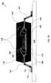
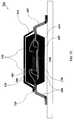
- FIG. 5Aillustrates a cross sectional view of a cap 510 .
- FIG. 5Billustrates a bottom view of cap 510 , in accordance with an embodiment of the present invention.
- Cap 510may be incorporated into various integrated circuit packages, such as shown in FIGS. 7A-7H , which are described in detail below.
- the packagesmay incorporate leadframes, such as shown in FIGS. 6A-6C , which are described in detail below.
- cap 510has a top portion 590 , sidewall portion 592 , and a rim 594 extending around a bottom periphery of cap 510 .
- Sidewall portion 592couples (e.g., electrically, structurally, and thermally) top portion 590 to rim 594 .
- sidewall portion 592is angled outward from top portion 590 .
- FIG. 5Aillustrates a planar top portion 590
- top portion 590can be non-planar (e.g., curved, concave, convex, hemispherical, or other shapes).
- sidewall portion 592may be perpendicular to or angled inward from top portion 590 .
- sidewall portion 592is not limited to a linear cross-section and may employ other cross-sectional shapes such as convex inward and outward as would be understood by one skilled in the art.
- Cap 510further has a first surface 580 and a second surface 585 .
- Second surface 585forms an upper surface of a cavity 570 in a bottom portion of cap 510 .
- Rim 594surrounds cavity 570 .
- Cavity 570is shown in FIG. 5A as having a trapezoidal cross section, but may have other shapes (e.g., square, rectangular, irregular, etc.).
- FIG. 5Billustrates cavity 570 having a circular shape, cavity 570 may have other shapes.
- cap 510may have various shapes such as round, rectangular, square, elliptical, oval, or any other shape.
- a bottom surface of rim 594has one or more protruding tabs 515 a - e .
- Tabs 515 a - emay have any shape.
- FIGS. 5A and 5Bshow a frustum tab 515 a , a conical tab 515 b , a pair 517 of conical tabs 515 c and 515 d , and an oblong shaped tab 515 e .
- Cap 510is not limited to the shapes, sizes, locations, or numbers of tabs 515 shown. Cap 510 may also have zero or more tabs of any shape, of any size, in any locations.
- the outer periphery dimension of cap 510is preferably the same size as the periphery (e.g., see FIG. 7C ) or smaller than the periphery (see FIG. 7A ) of the leadframe's “shoulder bends” to facilitate visual inspection of lead interconnect on the PCB.
- the outer periphery dimension of cap 510extends beyond the periphery of the leadframe's “shoulder bends”.
- the outer periphery of cap 510is preferably smaller than the dimension of the leadframe support ring 630 (e.g., see FIGS. 6A and 8C , further described below).
- cap 510is illustrated having a particular size, other sizes may be used, as would be understood by persons skilled in the relevant art(s).
- cap 510may be configured to mount an external heat sink (e.g., see FIG. 7F , further described below).
- cap 510may be configured to be thermally and/or electrically connected to a printed circuit board (PCB).
- PCBprinted circuit board
- cap 510may be coupled to the PCB (e.g., see FIGS. 7G and 7H , further described below).
- Cap 510may be made of a thermally conductive material and/or an electrically conductive material, such as a metal.
- the material for cap 510may include copper, a copper alloy, (e.g., C194, C151, C7025, or EFTEC 64T), aluminum, an aluminum alloy, ferromagnetic materials, laminated copper or iron, etc.
- Other metals and combinations of metals/alloys, or other thermally and electrically conductive materialse.g., ceramics, metallized plastics, laminated metal foils on plastic or ceramic, etc.
- Cap 510 and leadframe 110may be made of the same material or different materials.
- cap 510 and leadframe 110are made of the same material, or materials having the same coefficient of thermal expansion, structural integrity may be improved, such as reducing thermal stress on the die (sandwiched between the cap and leadframe).
- cap 510may have any thickness, depending on the particular application. For example, cap 510 may have a thickness of 0.1 to 0.5 mm. Alternatively, cap 510 may have a thickness of less than 1.0 mm.
- the bottom surface or portions of the bottom surface of rim 594may be coated or laminated with a layer of dielectric material (e.g. solder mask, dielectric film etc.). In this manner, the shorting of leads after assembly may be prevented.
- dielectric materiale.g. solder mask, dielectric film etc.
- cap 510may have openings through the first surface 580 and the second surface 585 .
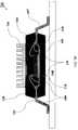
- FIGS. 5C and 5Dshow example caps 510 having openings or slots 520 formed in sidewall portions 592 , according to embodiments of the present invention.
- FIGS. 5C and 5Dillustrate slots 520 in sidewall portion 592 as rectangular or trapezoidal, slots 520 can have other shapes.
- cap 510may have holes/openings 530 in top portion 590 as illustrated in FIG. 5E , according to an example embodiment of the present invention.
- Cap 510may have any number of holes.
- holes 530can have any shape.
- holes 530 and slots 520allow the flow of encapsulating material 120 into cavity 570 during a manufacturing process. Additionally or alternatively, slots 520 and holes 530 may release pressure buildup (during or after manufacture) occurring in cavity 570 . Because smaller holes 530 and slots 520 may require a higher pressure to flow or inject encapsulating material 120 into cavity 570 , larger holes 530 and slots 520 may be desirable from a manufacturing perspective. However, in an embodiment, cap 510 may require the size of holes 530 and slots 520 to be limited to reduce EMI penetration. In an embodiment, a hole 530 or slot 520 diameter is in the range of 0.5-3.0 mm.
- a diameter 1.5 mmmay be used to shield against EMI having a highest harmonic frequency of about 10 GHz.
- An outer surface of cap 510may be completely or partially encapsulated in encapsulating material 120 , or may have no encapsulating material 120 covering it.
- Example embodiments for leadframe structuresare described in this section. Further embodiments will become apparent to persons having skill in the relevant art(s) from the teachings herein. Elements of the leadframe embodiments described herein can be combined in any manner.
- FIGS. 6A-6Cillustrate various leadframe structures, according to example embodiments of the present invention.
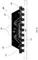
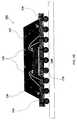
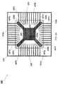
- FIG. 6Ashows a leadframe 600 having a die attach pad (DAP) 605 , a plurality of leads 607 , a plurality of tie bars 620 , an inner support ring 630 , and a perimeter support ring 632 .
- leadframe 600is rectangular in shape, having a rectangular perimeter support ring 632 surrounding its periphery.
- Perimeter support ring 632includes a first perimeter edge 634 a , a second perimeter edge 634 b , a third perimeter edge 634 c , and a fourth perimeter edge 634 d , coupled in a rectangular ring.
- DAP 605is centered in leadframe 600 .
- DAP 605is rectangular in shape.
- tie-bars 610extend outward from the four comers of DAP 605 .
- Leads 607extend inward perpendicularly from perimeter support ring 632 . Leads 607 are also coupled to inner support ring 630 , which forms a rectangular shape surrounding DAP 605 . Leads 607 a - h are coupled to tie bars 620 . Lead 607 a is coupled between edge 634 a of lead frame 600 and tie bar 620 a . Lead 607 b is coupled between edge 634 a of lead frame 600 and tie bar 620 b . Lead 607 c is coupled between edge 634 b of lead frame 600 and tie bar 620 b . Lead 607 d is coupled between edge 634 b of lead frame 600 and tie bar 620 c .
- Lead 607 eis coupled between edge 634 c of lead frame 600 and tie bar 620 c .
- Lead 607 fis coupled between edge 634 c of lead frame 600 and tie bar 620 d .
- Lead 607 gis coupled between edge 634 d of lead frame 600 and tie bar 620 d .
- Lead 607 his coupled between edge 634 d of lead frame 600 and tie bar 620 a .
- Leads 607are supported by perimeter support ring 632 and inner support ring 630 in lead frame 600 .
- Leads 607(except leads 607 a - h ) include an inner lead portion 636 within inner support ring 630 that are generally oriented radially with respect to a center leadframe 600 .
- FIGS. 6A-6Cillustrate a square leadframe 600 , DAP 605 , and inner support ring 630 , other shapes could also be employed (e.g., rectangle, circle, ellipse, curvilinear rectangle, etc).
- the number of leads 607is not limited by FIG. 6A , and in embodiment, leadframes may have any number of leads 607 .
- tie-bar 610may be widened, and may be located at other positions around DAP 605 than shown in FIG. 6A . Any number of leads 607 may be fused to a tie-bar, which may further effectively widen the tie-bar.
- FIG. 6Bshows a tie-bar 620 x coupled between DAP 605 and first and second leads 607 x and 607 y at a point 640 .
- Leadframe 600may have one or more fused tie bar leads 620 , widened fused leads 640 , or both. Alternatively, leadframe 600 may have no widened fused leads 640 nor fused tie-bar leads 620 .
- lead frame 600may have one or more tie bars 610 that are not coupled to leads 607 .
- tie-bars 620 a - dhave receptacles 615 formed therein.
- Receptacles 615correspond to tabs 515 formed in a cap 510 .
- receptacles 615can include a rectangular shaped receptacle 615 a , a pair 617 of conical shaped receptacles 615 b and 615 c , a pair 619 of rounded receptacles 615 d and 615 e , and a rounded receptacle 615 f .
- receptacles 615are not limited to these shapes, combinations of shapes, numbers, locations, or sizes.
- Receptacles 615may be indentions (not fully penetrating the leadframe 600 ) or may be cut-outs (fully penetrating the leadframe 600 ).
- Leadframe 600may have any number of receptacles 615 of any size, shape, and in locations. Receptacles 615 on leadframe 600 are configured to couple with tabs 515 on a cap 510 providing increased structural strength, as well as enhanced thermal and electrical connection.
- Example materials for leadframe 600include metals, such as copper, copper alloy, (e.g., C194, C151, C7025, or EFTEC 64T), aluminum, aluminum alloys, ferromagnetic materials, other metals and combinations of metals/alloys, or other thermally and electrically conductive materials.
- Cap 510 and leadframe 600may be made of the same material or different materials.
- Leadframe 600may be any thickness depending on the particular application. For example, leadframe 600 thickness may range from 0.05 mm to 0.5 mm. In another embodiment, leadframe 600 is less than 1.17 mm thick.
- leadframe 600provides stiffening and/or structural support to an IC package. In another embodiment, leadframe 600 provides heat spreading to an IC package. In another embodiment, leadframe 600 is electrically conductive, and can act as a power or ground plane for an IC package. In embodiments, leadframe 600 can be configured to provide any combination of stiffening, heat spreading, and electrical conductivity, as required by the particular application.
- Example embodiments for IC packagesare described in this section. Further embodiments will become apparent to persons having skill in the relevant art(s) from the teachings herein. Elements of the IC package embodiments described herein can be combined in any manner.
- FIG. 7Ashows an example IC package 700 , according to an embodiment of the invention.
- cap 510is coupled to leadframe 600 .
- a die 150is mounted on the same side of DAP 605 as cap 510 .
- Leadframe 600 and cap 510form an enclosure structure 702 that substantially encloses die 150 , providing improved structural integrity, EMI shielding, thermal performance, and environmental (e.g., mechanical shock, vibration, caustic, moisture, and radiation) protection.
- additional dies and/or other electrical componentscan be attached to DAP 605 .
- cap 510 and leadframe 600are made of copper or copper alloys.
- the thermal conductivity of copper(roughly 390 W/m ⁇ K) is much greater than for typical encapsulating materials 120 (0.2-0.9 W/m ⁇ K). Therefore, the heat generated by die 150 is conducted through adhesive 170 to DAP 605 and out of the package through leads 607 and cap 510 .
- cap 510 and leadframe 600are electrically connected, they may form a near-equipotential surface, such that enclosure structure 702 approximates an ideal Faraday Cage. In this manner, die 150 is isolated from external EMI. Additionally, external devices are also shielded from EMI generated by die 150 .
- copper and copper alloyshave a much higher modulus of elasticity (about 125 GPa) compared to a typical cured plastic molding compound used for encapsulating material 120 (about 25 GPa), copper embodiments of the present invention provide improved structural rigidity and environmental protection.
- cap 510 and leadframe 600are coupled together without the use of tabs and receptacles.
- cap 510has tabs 515 which fit corresponding receptacles 615 .
- Tabs 515 and corresponding receptacles 615may facilitate tight lock-in of the cap 510 to leadframe 600 .
- the configuration of tabs 515 and receptacles 615are such that cap 510 will mate correctly with leadframe 600 in only one orientation, which may facilitate assembly.
- cap 510may have receptacles that interlock with tabs of leadframe 600 .
- Thermally and/or electrically conductive adhesive materialsmay be used to improve the coupling between cap 510 and leadframe 600 .
- An adhesive materialcan be used to attach a tab 515 and a receptacle 615 , when they are present. Alternatively, the adhesive material may be used at areas where cap 510 contacts leadframe 600 .
- Leadframe 600may be plated with a conductive material to improve the thermal and electrical connection.
- cap 510may be mounted to DAP 605 of leadframe 600 .
- cap 510is mounted to tie-bars 620 coupled between DAP 605 and leads 607 .
- cap 510may be mounted to one or more leads 607 .
- cap 510can be mounted to any combination of DAP 605 , tie bars 620 , and leads 607 .
- portions of the bottom surface, or all of the bottom surface of rim 594 of cap 510may be coated with a layer of dielectric material (e.g. solder mask, dielectric film etc.) to prevent electrical shorting with one or more of leads 607 .
- dielectric materiale.g. solder mask, dielectric film etc.
- lead 607 of leadframe 600are shaped to be coupled to a PCB.
- an outer portion of leads 607 extending from package 700may be bent to allow leads 607 to contact a PCB.
- leads 607may be bent to form an “L” or “hockey stick” type shape, having a first bend 720 , and a second bend 722 .
- End portion 724 of leads 607can be coupled to PCB 160 , as shown in FIG. 7A .
- leads 607may be bent toward a side of package 700 away from die 150 to form a “die up” package.
- leads 607may be bent toward a side of the package toward die 150 to form a “die down” package, (such as shown in FIGS. 7G and 7H ).
- Integrating an encapsulating material, such as glob top or plastic molding compound, with an enclosure structure, such as enclosure structure 702may enhance the structural rigidity and planarity of the IC package.
- the combination of the encapsulating material and the enclosure structuremay reduce IC die cracking and delamination.
- Integrating the encapsulating material with the enclosure structurealso enhances environmental protection.
- the integrated packagecan provide protection against mechanical stress, impact, vibration, chemical corrosives, moistures, heat exposure, radiation, etc.
- attaching the IC die directly to the enclosure structureadds mass to the die support, and helps reduce microphonics.
- the metal traces of the IC diehave electrical resistance, capacitance, and inductance.
- the IC dieis under mechanical stress. Vibration, mechanical shock, or sudden change of temperature can cause a change of stress distribution within the IC die, and thus alter a capacitance and resistance such that a voltage vibration or drift is produced. This phenomenon is called microphonics. Attachment of the semiconductor die directly to the enclosure structure increases the mass and helps dampen these mechanical shocks and vibrations, thus reducing microphonics.
- Typical encapsulating materialssuch as plastic molding compound, have low thermal conductivity (e.g., about 0.2 to 0.9 W/m ⁇ K) and therefore create a bottleneck for heat dissipation in conventional IC packages.
- the enclosure structureeliminates this bottleneck by providing a thermally conductive path from the bottom surface of the IC die to the outer surfaces of the package.
- the enclosure structureis made with materials that have high thermal conductivity (e.g., approximately 390 W/m ⁇ K for copper) and therefore promote heat dissipation.
- Enclosure structure 702 formed by cap 510 and leadframe 600may be incorporated into IC packages of many different configurations.
- FIGS. 7A-7Hillustrate some example embodiments of the present invention.
- package 700 of FIG. 7Ashows die 150 attached to a DAP 605 with a thermally and/or electrically conductive adhesive 170 (such as an epoxy with metal or other conductive particles or flakes, solder, etc.) that is electrically connected through wirebond 130 , DAP 605 and leads 607 .
- a thermally and/or electrically conductive adhesive 170such as an epoxy with metal or other conductive particles or flakes, solder, etc.
- package 700is encapsulated in encapsulating material 120 .
- Package 700may be mounted to a printed circuit board (PCB) 160 , including printed wiring boards (PWBs).
- PCBprinted circuit board
- PWBsprinted wiring boards
- at least one wirebond 130couples at least one bond pad (not shown) on a surface of IC die 150 to leadframe 600 .
- one of the bond padsis a ground pad.
- an packagemay include a cap 510 having one or more openings (e.g. slots 520 and/or holes 530 ) as described elsewhere herein. These openings may act as mold gate openings, allowing encapsulating material 120 to flow or be injected into cavity 570 .
- cap 510has a surface 704 that is exposed through the molding material 120 encapsulating package 700 .
- encapsulating material 120does not cover the entirety of first surface 580 of cap 510 .
- second surface 585 of cap 510is covered by encapsulating material 120 .
- FIG. 7Billustrates an embodiment where both first surface 580 and second surface 585 of cap 510 are covered by encapsulating material 120 .
- FIG. 7Cillustrates an embodiment where first and second surfaces 580 and 585 of cap 510 are not covered by encapsulating material 120 .
- An IC packagemay be in the form of this embodiment if cap 510 is added to package 704 after encapsulating material 120 (e.g., a molding compound) has been applied.
- leadframe 600may have tie bars 620 on a different plane than the leadframe bond fingers or leads 750 .
- tie bars 620are above leads 750 .
- tie bars 620are below leads 750 .
- the embodiment of FIG. 7Ehas the advantage of requiring shorter wirebonds 130 from the top of IC die 150 to leads 750 , relative to the embodiment of FIG. 7D .
- FIG. 7Fshows an IC package 710 where cap 510 is configured to mount an external heat sink 730 .
- Leadframe 600 and cap 510provide a path for heat to be conducted from die 150 to heat sink 730 , and thus out of package 710 .
- FIG. 7Gillustrates a package 712 in a die-down configuration, according to an example embodiment of the present invention.
- surface 580 of cap 510is exposed on the bottom side of package 712 .
- the features reflected in the embodiments illustrated in FIGS. 7A-7Fare applicable to the die-down configuration embodiment illustrated in FIGS. 7G and 7H .
- FIG. 7Hillustrates a package 714 , according to another embodiment of the present invention. In package 714 , exposed surface 580 of cap 510 is coupled to PCB 160 with electrically and/or thermally conductive adhesive or solder 740 .
- heat conducted from IC die 150 through leadframe 600 and cap 510may be conducted out of package 714 into PCB 160 .
- Surface 580 of cap 510may be electrically connected to a power pad or pads (not shown in FIG. 7H ) on PCB 160 to improve EMI shielding and power delivery from package 714 .
- surface 580 of cap 510may be electrically connected to ground pad or pads (not shown in FIG. 7H ) on PCB 160 to improve EMI shielding and current return from package 714 .
- FIG. 10Ashows flowchart 1000 illustrating example steps to assemble leadframe package 700 shown in FIG. 7A , according to an embodiment of the present invention.
- FIG. 10Bshows flowchart 1050 illustrating example steps for an alternate method to assemble package 700 .
- adaptation of these assembly processescould be used to assemble any embodiments, including those illustrated in FIGS. 7A-7H .
- the steps in FIGS. 10A and 10Bdo not necessarily have to occur in the order shown, as will be apparent to persons skilled in the relevant art(s) based on the teachings herein. Other operational and structural embodiments will be apparent to persons skilled in the relevant art(s) based on the following discussion. These steps are described in detail below with respect to FIGS. 8A-8D and 9 A- 9 C, for illustrative purposes.
- FIGS. 8A-8Dillustrate top views and FIGS. 9A-9C show side views of embodiments of the invention at different stages of assembly.
- Flowchart 1000is shown in FIG. 10A , and begins with step 1005 .
- a leadframe 600is formed from a sheet of material.
- Example leadframe material and featuresare discussed elsewhere herein.
- FIG. 8Aillustrates a view of a single leadframe 600 .
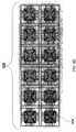
- FIG. 8Billustrates an example leadframe panel 800 that contains an array of leadframes 600 .
- Leadframes 600 in leadframe panel 800are manufactured by an etching or stamping process, for example.
- step 1010at least one IC die 150 is attached to a DAP 605 of a leadframe 600 .
- IC die 150is attached using a thermally and/or electrically conductive adhesive 170 (such as solder or epoxy containing metal or other conductive particles or flakes).
- FIG. 9Aillustrates a side view of an embodiment at this stage of assembly.
- wirebond 130are used to attach pads of IC die 150 to leadframe 600 , providing electrical connections from IC die 150 to leads 607 , tie bars 610 , and/or DAP 605 .
- cap 150is attached to the leadframe 600 .
- Electrically and/or thermally conductive adhesive materialsmay be used to improve coupling between cap 510 and leadframe 600 .
- Cap 510 and leadframe 600are joined to form an enclosure structure (e.g., enclosure structure 702 ) which substantially encloses IC die 150 .
- FIG. 8Cshows a partially assembled package 810 , illustrating an example embodiment leadframe package at this stage of assembly.
- FIG. 8Dillustrates a partially assembled panel 820 of partially assembled packages 810 .
- FIG. 9Bshows a side view of partially assembled panel 820 .
- an encapsulating processencapsulates partially assembled package 810 in encapsulating material 120 .
- the package or packages 810may be clamped in a mold chassis to mold or shape a molding compound being used to encapsulate the package.
- FIG. 9Cshows a side view of an encapsulated panel 910 of leadframe packages 700 at this stage of assembly.
- an outer peripheral dimension of a cap 510is smaller than a peripheral dimension of peripheral support ring 630 . This prevents the encapsulating material from bleeding through gaps between leads 607 .
- Inner support ring 630may also provide sealing between the clamped mold chassis during the transfer molding process.
- Leadframe support ring 630is trimmed in step 1030 .
- Leads 607are ready to be formed into contact pins for board mount and a leadframe package 700 is completely assembled.
- the outer portion of leads 607 extending from the packagemay be bent to allow them to contact a PCB.
- leads 607may be bent to form an “L” or “hockey stick” type shape.
- leads 607may be bent toward a side of the package away from die 150 to form a “die up” package, or may be bent toward a side of the package toward die 150 to form a “die down” package.
- Steps 1005 - 1015are the same as shown in FIG. 10A .
- a leadframe 600 and a cap 510are put into the mold chassis for steps 1055 and 1060 .
- step 1065a molding process takes place.
- leadframe 600 and cap 510are coupled together, and in an embodiment, may be held together by a molding compound.
Landscapes
- Engineering & Computer Science (AREA)
- Microelectronics & Electronic Packaging (AREA)
- Computer Hardware Design (AREA)
- Power Engineering (AREA)
- Physics & Mathematics (AREA)
- General Physics & Mathematics (AREA)
- Condensed Matter Physics & Semiconductors (AREA)
- Chemical & Material Sciences (AREA)
- Materials Engineering (AREA)
- Health & Medical Sciences (AREA)
- Electromagnetism (AREA)
- Toxicology (AREA)
- Lead Frames For Integrated Circuits (AREA)
Abstract
Description
Claims (15)
Priority Applications (1)
| Application Number | Priority Date | Filing Date | Title |
|---|---|---|---|
| US12/535,548US7781266B2 (en) | 2005-10-20 | 2009-08-04 | Methods and apparatus for improved thermal performance and electromagnetic interference (EMI) shielding in leadframe integrated circuit (IC) packages |
Applications Claiming Priority (2)
| Application Number | Priority Date | Filing Date | Title |
|---|---|---|---|
| US11/253,714US7582951B2 (en) | 2005-10-20 | 2005-10-20 | Methods and apparatus for improved thermal performance and electromagnetic interference (EMI) shielding in leadframe integrated circuit (IC) packages |
| US12/535,548US7781266B2 (en) | 2005-10-20 | 2009-08-04 | Methods and apparatus for improved thermal performance and electromagnetic interference (EMI) shielding in leadframe integrated circuit (IC) packages |
Related Parent Applications (1)
| Application Number | Title | Priority Date | Filing Date |
|---|---|---|---|
| US11/253,714DivisionUS7582951B2 (en) | 2005-10-20 | 2005-10-20 | Methods and apparatus for improved thermal performance and electromagnetic interference (EMI) shielding in leadframe integrated circuit (IC) packages |
Publications (2)
| Publication Number | Publication Date |
|---|---|
| US20100035383A1 US20100035383A1 (en) | 2010-02-11 |
| US7781266B2true US7781266B2 (en) | 2010-08-24 |
Family
ID=37984576
Family Applications (2)
| Application Number | Title | Priority Date | Filing Date |
|---|---|---|---|
| US11/253,714Expired - Fee RelatedUS7582951B2 (en) | 2005-10-20 | 2005-10-20 | Methods and apparatus for improved thermal performance and electromagnetic interference (EMI) shielding in leadframe integrated circuit (IC) packages |
| US12/535,548Expired - Fee RelatedUS7781266B2 (en) | 2005-10-20 | 2009-08-04 | Methods and apparatus for improved thermal performance and electromagnetic interference (EMI) shielding in leadframe integrated circuit (IC) packages |
Family Applications Before (1)
| Application Number | Title | Priority Date | Filing Date |
|---|---|---|---|
| US11/253,714Expired - Fee RelatedUS7582951B2 (en) | 2005-10-20 | 2005-10-20 | Methods and apparatus for improved thermal performance and electromagnetic interference (EMI) shielding in leadframe integrated circuit (IC) packages |
Country Status (1)
| Country | Link |
|---|---|
| US (2) | US7582951B2 (en) |
Cited By (34)
| Publication number | Priority date | Publication date | Assignee | Title |
|---|---|---|---|---|
| US20090284932A1 (en)* | 2008-03-25 | 2009-11-19 | Bridge Semiconductor Corporation | Thermally Enhanced Package with Embedded Metal Slug and Patterned Circuitry |
| US20100003787A1 (en)* | 2008-03-25 | 2010-01-07 | Bridge Semiconductor Corporation | Method of making a semiconductor chip assembly with a post/base heat spreader and horizontal signal routing |
| US20100052005A1 (en)* | 2008-03-25 | 2010-03-04 | Lin Charles W C | Semiconductor chip assembly with post/base heat spreader and conductive trace |
| US20100059786A1 (en)* | 2008-03-25 | 2010-03-11 | Lin Charles W C | Semiconductor chip assembly with post/base heat spreader and substrate |
| US20100072511A1 (en)* | 2008-03-25 | 2010-03-25 | Lin Charles W C | Semiconductor chip assembly with copper/aluminum post/base heat spreader |
| US20100072510A1 (en)* | 2008-03-25 | 2010-03-25 | Lin Charles W C | Semiconductor chip assembly with post/base/cap heat spreader |
| US20100096662A1 (en)* | 2008-03-25 | 2010-04-22 | Bridge Semiconductor Corporation | Semiconductor chip assembly with post/base heat spreader and signal post |
| US20100155769A1 (en)* | 2008-03-25 | 2010-06-24 | Bridge Semiconductor Corporation | Semiconductor chip assembly with base heat spreader and cavity in base |
| US20100155768A1 (en)* | 2008-03-25 | 2010-06-24 | Bridge Semiconductor Corporation | Semiconductor chip assembly with post/base heat spreader and cavity in post |
| US20100181594A1 (en)* | 2008-03-25 | 2010-07-22 | Lin Charles W C | Semiconductor chip assembly with post/base heat spreader and cavity over post |
| US20100193830A1 (en)* | 2008-03-25 | 2010-08-05 | Bridge Semiconductor Corporation | Semiconductor chip assembly with post/base heat spreader and dual adhesives |
| US20100270660A1 (en)* | 2009-04-28 | 2010-10-28 | Dai Nippon Printing Co., Ltd. | Semiconductor device and method for manufacturing metallic shielding plate |
| US20100289054A1 (en)* | 2008-03-25 | 2010-11-18 | Bridge Semiconductor Corporation | Semiconductor chip assembly with post/base heat spreader and adhesive between base and terminal |
| US20100327310A1 (en)* | 2008-03-25 | 2010-12-30 | Lin Charles W C | Semiconductor chip assembly with post/base/flange heat spreader and cavity in flange |
| US20110039374A1 (en)* | 2008-03-25 | 2011-02-17 | Bridge Semiconductor Corporation | Method of making a semiconductor chip assembly with a bump/base heat spreader and a cavity in the bump |
| US20110065241A1 (en)* | 2008-03-25 | 2011-03-17 | Bridge Semiconductor Corporation | Method of making a semiconductor chip assembly with a bump/base heat spreader and a dual-angle cavity in the bump |
| US20110101410A1 (en)* | 2008-03-25 | 2011-05-05 | Lin Charles W C | Semiconductor chip assembly with post/base/post heat spreader |
| US20110151626A1 (en)* | 2008-03-25 | 2011-06-23 | Lin Charles W C | Method of making a semiconductor chip assembly with a post/base/post heat spreader and asymmetric posts |
| US20110163348A1 (en)* | 2008-03-25 | 2011-07-07 | Bridge Semiconductor Corporation | Semiconductor chip assembly with bump/base heat spreader and inverted cavity in bump |
| US20110198662A1 (en)* | 2008-03-25 | 2011-08-18 | Bridge Semiconductor Corporation | Semiconductor chip assembly with post/base heat spreader and multilevel conductive trace |
| US8003415B2 (en) | 2008-03-25 | 2011-08-23 | Bridge Semiconductor Corporation | Method of making a semiconductor chip assembly with a post/base heat spreader and vertical signal routing |
| US8110446B2 (en) | 2008-03-25 | 2012-02-07 | Bridge Semiconductor Corporation | Method of making a semiconductor chip assembly with a post/base heat spreader and a conductive trace |
| US8129742B2 (en) | 2008-03-25 | 2012-03-06 | Bridge Semiconductor Corporation | Semiconductor chip assembly with post/base heat spreader and plated through-hole |
| US8153477B2 (en) | 2008-03-25 | 2012-04-10 | Bridge Semiconductor Corporation | Method of making a semiconductor chip assembly with a post/dielectric/post heat spreader |
| US8178395B2 (en) | 2008-03-25 | 2012-05-15 | Bridge Semiconductor Corporation | Method of making a semiconductor chip assembly with a post/base heat spreader with a thermal via |
| US8212279B2 (en) | 2008-03-25 | 2012-07-03 | Bridge Semiconductor Corporation | Semiconductor chip assembly with post/base heat spreader, signal post and cavity |
| US8232576B1 (en) | 2008-03-25 | 2012-07-31 | Bridge Semiconductor Corporation | Semiconductor chip assembly with post/base heat spreader and ceramic block in post |
| US8304292B1 (en) | 2009-08-06 | 2012-11-06 | Bridge Semiconductor Corporation | Method of making a semiconductor chip assembly with a ceramic/metal substrate |
| US8310043B2 (en) | 2008-03-25 | 2012-11-13 | Bridge Semiconductor Corporation | Semiconductor chip assembly with post/base heat spreader with ESD protection layer |
| US8329510B2 (en) | 2008-03-25 | 2012-12-11 | Bridge Semiconductor Corporation | Method of making a semiconductor chip assembly with a post/base heat spreader with an ESD protection layer |
| US8354688B2 (en) | 2008-03-25 | 2013-01-15 | Bridge Semiconductor Corporation | Semiconductor chip assembly with bump/base/ledge heat spreader, dual adhesives and cavity in bump |
| US10654709B1 (en) | 2018-10-30 | 2020-05-19 | Nxp Usa, Inc. | Shielded semiconductor device and lead frame therefor |
| US10892229B2 (en) | 2019-04-05 | 2021-01-12 | Nxp Usa, Inc. | Media shield with EMI capability for pressure sensor |
| US11049817B2 (en) | 2019-02-25 | 2021-06-29 | Nxp B.V. | Semiconductor device with integral EMI shield |
Families Citing this family (61)
| Publication number | Priority date | Publication date | Assignee | Title |
|---|---|---|---|---|
| US7271479B2 (en)* | 2004-11-03 | 2007-09-18 | Broadcom Corporation | Flip chip package including a non-planar heat spreader and method of making the same |
| US7566591B2 (en)* | 2005-08-22 | 2009-07-28 | Broadcom Corporation | Method and system for secure heat sink attachment on semiconductor devices with macroscopic uneven surface features |
| US7582951B2 (en) | 2005-10-20 | 2009-09-01 | Broadcom Corporation | Methods and apparatus for improved thermal performance and electromagnetic interference (EMI) shielding in leadframe integrated circuit (IC) packages |
| US7692295B2 (en)* | 2006-03-31 | 2010-04-06 | Intel Corporation | Single package wireless communication device |
| TWI321350B (en)* | 2006-04-18 | 2010-03-01 | Advanced Semiconductor Eng | Heatsink and heatsink positioning system |
| US7714453B2 (en)* | 2006-05-12 | 2010-05-11 | Broadcom Corporation | Interconnect structure and formation for package stacking of molded plastic area array package |
| US9299634B2 (en)* | 2006-05-16 | 2016-03-29 | Broadcom Corporation | Method and apparatus for cooling semiconductor device hot blocks and large scale integrated circuit (IC) using integrated interposer for IC packages |
| US8183680B2 (en) | 2006-05-16 | 2012-05-22 | Broadcom Corporation | No-lead IC packages having integrated heat spreader for electromagnetic interference (EMI) shielding and thermal enhancement |
| US20070273023A1 (en)* | 2006-05-26 | 2007-11-29 | Broadcom Corporation | Integrated circuit package having exposed thermally conducting body |
| US7808087B2 (en)* | 2006-06-01 | 2010-10-05 | Broadcom Corporation | Leadframe IC packages having top and bottom integrated heat spreaders |
| US9013035B2 (en)* | 2006-06-20 | 2015-04-21 | Broadcom Corporation | Thermal improvement for hotspots on dies in integrated circuit packages |
| US8581381B2 (en) | 2006-06-20 | 2013-11-12 | Broadcom Corporation | Integrated circuit (IC) package stacking and IC packages formed by same |
| US7479692B2 (en)* | 2006-11-09 | 2009-01-20 | Stats Chippac Ltd. | Integrated circuit package system with heat sink |
| KR100947454B1 (en)* | 2006-12-19 | 2010-03-11 | 서울반도체 주식회사 | Multi-stage heat transfer slug and light emitting diode package using the same |
| US8183687B2 (en)* | 2007-02-16 | 2012-05-22 | Broadcom Corporation | Interposer for die stacking in semiconductor packages and the method of making the same |
| US7872335B2 (en)* | 2007-06-08 | 2011-01-18 | Broadcom Corporation | Lead frame-BGA package with enhanced thermal performance and I/O counts |
| US8283757B2 (en)* | 2007-07-18 | 2012-10-09 | Mediatek Inc. | Quad flat package with exposed common electrode bars |
| US20090045503A1 (en)* | 2007-08-17 | 2009-02-19 | Koduri Sreenivasan K | Multidirectional Semiconductor Device Package Thermal Enhancement Systems and Methods |
| US8097934B1 (en)* | 2007-09-27 | 2012-01-17 | National Semiconductor Corporation | Delamination resistant device package having low moisture sensitivity |
| EP2120263A4 (en)* | 2007-11-30 | 2010-10-13 | Panasonic Corp | HEAT DISSIPATING STRUCTURE BASE PLATE, MODULE USING HEAT DISSIPATING STRUCTURE BASE PLATE, AND METHOD FOR MANUFACTURING HEAT DISSIPATING STRUCTURE BASE PLATE |
| US8507319B2 (en)* | 2007-12-07 | 2013-08-13 | Stats Chippac Ltd. | Integrated circuit package system with shield |
| US7902644B2 (en)* | 2007-12-07 | 2011-03-08 | Stats Chippac Ltd. | Integrated circuit package system for electromagnetic isolation |
| US7714419B2 (en)* | 2007-12-27 | 2010-05-11 | Stats Chippac Ltd. | Integrated circuit package system with shielding |
| US8502371B2 (en)* | 2007-12-27 | 2013-08-06 | Stats Chippac Ltd. | Integrated circuit package system with extended corner leads |
| US20090261462A1 (en)* | 2008-04-16 | 2009-10-22 | Jocel Gomez | Semiconductor package with stacked die assembly |
| US8072047B2 (en)* | 2008-05-21 | 2011-12-06 | Stats Chippac Ltd. | Integrated circuit package system with shield and tie bar |
| TW201013881A (en)* | 2008-09-10 | 2010-04-01 | Renesas Tech Corp | Semiconductor device and method for manufacturing same |
| JP2011054640A (en)* | 2009-08-31 | 2011-03-17 | Funai Electric Co Ltd | Shield package substrate |
| ITMI20092050A1 (en)* | 2009-11-23 | 2011-05-24 | Siae Microelettronica Spa | SHOCK ABSORBER DEVICE FOR INTEGRATED MICROWAVE OPERATING CIRCUITS AND RELATED DAMPING CIRCUIT |
| US10111333B2 (en) | 2010-03-16 | 2018-10-23 | Intersil Americas Inc. | Molded power-supply module with bridge inductor over other components |
| KR101362398B1 (en) | 2012-07-10 | 2014-02-13 | 앰코 테크놀로지 코리아 주식회사 | Semiconductor package and manufacturing method thereof |
| US8354747B1 (en)* | 2010-06-01 | 2013-01-15 | Amkor Technology, Inc | Conductive polymer lid for a sensor package and method therefor |
| US9723766B2 (en) | 2010-09-10 | 2017-08-01 | Intersil Americas LLC | Power supply module with electromagnetic-interference (EMI) shielding, cooling, or both shielding and cooling, along two or more sides |
| US9362209B1 (en) | 2012-01-23 | 2016-06-07 | Amkor Technology, Inc. | Shielding technique for semiconductor package including metal lid |
| JP5956783B2 (en)* | 2012-03-02 | 2016-07-27 | ルネサスエレクトロニクス株式会社 | Manufacturing method of semiconductor device |
| CN102779811B (en)* | 2012-07-20 | 2015-02-04 | 华为技术有限公司 | Chip package and chip packaging method |
| KR101971282B1 (en) | 2012-12-24 | 2019-04-22 | 에스케이하이닉스 주식회사 | Package substrate with band stop filter and semiconductor package including the same |
| JP6266219B2 (en)* | 2013-03-18 | 2018-01-24 | ルネサスエレクトロニクス株式会社 | Semiconductor device |
| JP5626402B2 (en)* | 2013-04-24 | 2014-11-19 | 大日本印刷株式会社 | Semiconductor device, method for manufacturing semiconductor device, and shield plate |
| US9445491B2 (en)* | 2013-09-04 | 2016-09-13 | Apple Inc. | Overpass grounding spring and integrated component protection |
| CN104576565A (en)* | 2013-10-18 | 2015-04-29 | 飞思卡尔半导体公司 | Semiconductor device provided with radiator and assembly method of semiconductor device |
| JP6312527B2 (en)* | 2014-05-23 | 2018-04-18 | 新日本無線株式会社 | Electronic component mounting structure with heat sink |
| US9165855B1 (en)* | 2014-07-02 | 2015-10-20 | Freescale Semiconductor, Inc. | Semiconductor device with die attached heat spreader |
| US9147656B1 (en)* | 2014-07-11 | 2015-09-29 | Freescale Semicondutor, Inc. | Semiconductor device with improved shielding |
| WO2016053966A2 (en)* | 2014-09-30 | 2016-04-07 | Henkel IP & Holding GmbH | Temperature regulation using phase change materials contained in an emi can |
| US9379034B1 (en)* | 2014-12-30 | 2016-06-28 | Stmicroelectronics Pte Ltd | Method of making an electronic device including two-step encapsulation and related devices |
| US9860987B2 (en) | 2015-02-13 | 2018-01-02 | Deere & Company | Electronic assembly with one or more heat sinks |
| US9693488B2 (en) | 2015-02-13 | 2017-06-27 | Deere & Company | Electronic assembly with one or more heat sinks |
| US9337140B1 (en) | 2015-09-01 | 2016-05-10 | Freescale Semiconductor, Inc. | Signal bond wire shield |
| CN108029228A (en)* | 2015-09-29 | 2018-05-11 | 日立汽车系统株式会社 | Electronic control unit |
| EP3168871B1 (en)* | 2015-11-11 | 2020-01-08 | Nexperia B.V. | Semiconductor device and a method of making a semiconductor device |
| US10043763B2 (en)* | 2015-12-19 | 2018-08-07 | Skyworks Solutions, Inc. | Shielded lead frame packages |
| US10120424B2 (en)* | 2017-01-19 | 2018-11-06 | Intel Corporation | Conductive stress-relief washers in microelectronic assemblies |
| WO2018142864A1 (en)* | 2017-02-06 | 2018-08-09 | 富士電機株式会社 | Semiconductor module, electric vehicle, and power control unit |
| US10490915B2 (en)* | 2017-06-07 | 2019-11-26 | Mitas Electronics, Llc | Gaussian chamber cable direct connector |
| KR102711765B1 (en)* | 2019-03-06 | 2024-09-27 | 삼성전기주식회사 | Electronic device module and manufacturing method thereof |
| KR102710329B1 (en) | 2019-06-21 | 2024-09-27 | 삼성전자주식회사 | Semiconductor Package |
| US11521918B2 (en)* | 2019-07-08 | 2022-12-06 | Amkor Technology Singapore Holding Pte. Ltd. | Semiconductor device having component mounted on connection bar and lead on top side of lead frame and method of manufacturing semiconductor device thereof |
| US11901309B2 (en)* | 2019-11-12 | 2024-02-13 | Semiconductor Components Industries, Llc | Semiconductor device package assemblies with direct leadframe attachment |
| US11694970B2 (en) | 2021-03-19 | 2023-07-04 | Nxp B.V. | Plated pillar dies having integrated electromagnetic shield layers |
| US20240258245A1 (en)* | 2023-01-26 | 2024-08-01 | Texas Instruments Incorporated | Molded module package with an emi shielding barrier |
Citations (93)
| Publication number | Priority date | Publication date | Assignee | Title |
|---|---|---|---|---|
| GB1306031A (en) | 1971-01-01 | 1973-02-07 | ||
| US4480262A (en) | 1982-07-15 | 1984-10-30 | Olin Corporation | Semiconductor casing |
| US4560826A (en) | 1983-12-29 | 1985-12-24 | Amp Incorporated | Hermetically sealed chip carrier |
| US4680613A (en) | 1983-12-01 | 1987-07-14 | Fairchild Semiconductor Corporation | Low impedance package for integrated circuit die |
| US4803544A (en)* | 1986-07-11 | 1989-02-07 | Junghans Uhren Gmbh | Prefabricated strip conductor network assembly unit and process for making same |
| US5105260A (en) | 1989-10-31 | 1992-04-14 | Sgs-Thomson Microelectronics, Inc. | Rf transistor package with nickel oxide barrier |
| US5153379A (en) | 1990-10-09 | 1992-10-06 | Motorola, Inc. | Shielded low-profile electronic component assembly |
| EP0573297A2 (en) | 1992-06-04 | 1993-12-08 | Shinko Electric Industries Co. Ltd. | Semiconductor device comprising a TAB tape |
| US5294826A (en) | 1993-04-16 | 1994-03-15 | Northern Telecom Limited | Integrated circuit package and assembly thereof for thermal and EMI management |
| US5350943A (en) | 1992-04-18 | 1994-09-27 | Temic Telefunken Microelectronic Gmbh | Semiconductor assembly, in particular a remote control reception module |
| US5376756A (en)* | 1991-12-20 | 1994-12-27 | Vlsi Technology, Inc. | Wire support and guide |
| US5389816A (en) | 1992-11-19 | 1995-02-14 | Shinko Electric Industries Co., Ltd. | Multi-layer lead frame using a metal-core substrate |
| US5406117A (en) | 1993-12-09 | 1995-04-11 | Dlugokecki; Joseph J. | Radiation shielding for integrated circuit devices using reconstructed plastic packages |
| US5457341A (en) | 1994-05-03 | 1995-10-10 | Texas Instruments Incorporated | Integrated circuit device and manufacturing method using photoresist lead covering |
| US5468910A (en) | 1993-08-02 | 1995-11-21 | Motorola, Inc. | Semiconductor device package and method of making |
| US5482720A (en)* | 1994-10-11 | 1996-01-09 | Church & Dwight Co., Inc. | Encapsulated co-micronized bicarbonate salt compositions |
| US5486720A (en) | 1994-05-26 | 1996-01-23 | Analog Devices, Inc. | EMF shielding of an integrated circuit package |
| US5497032A (en) | 1993-03-17 | 1996-03-05 | Fujitsu Limited | Semiconductor device and lead frame therefore |
| US5559306A (en) | 1994-05-17 | 1996-09-24 | Olin Corporation | Electronic package with improved electrical performance |
| US5608265A (en) | 1993-03-17 | 1997-03-04 | Hitachi, Ltd. | Encapsulated semiconductor device package having holes for electrically conductive material |
| US5614761A (en) | 1991-02-28 | 1997-03-25 | Hitachi, Ltd. | Electronic circuit package including plural semiconductor chips formed on a wiring substrate |
| US5642261A (en) | 1993-12-20 | 1997-06-24 | Sgs-Thomson Microelectronics, Inc. | Ball-grid-array integrated circuit package with solder-connected thermal conductor |
| US5650659A (en) | 1995-08-04 | 1997-07-22 | National Semiconductor Corporation | Semiconductor component package assembly including an integral RF/EMI shield |
| US5668406A (en) | 1994-05-31 | 1997-09-16 | Nec Corporation | Semiconductor device having shielding structure made of electrically conductive paste |
| US5691567A (en) | 1995-09-19 | 1997-11-25 | National Semiconductor Corporation | Structure for attaching a lead frame to a heat spreader/heat slug structure |
| US5703398A (en) | 1993-03-17 | 1997-12-30 | Fujitsu Limited | Semiconductor integrated circuit device and method of producing the semiconductor integrated circuit device |
| US5723899A (en) | 1994-08-30 | 1998-03-03 | Amkor Electronics, Inc. | Semiconductor lead frame having connection bar and guide rings |
| US5889316A (en) | 1993-06-18 | 1999-03-30 | Space Electronics, Inc. | Radiation shielding of plastic integrated circuits |
| US5977626A (en) | 1998-08-12 | 1999-11-02 | Industrial Technology Research Institute | Thermally and electrically enhanced PBGA package |
| US5986340A (en) | 1996-05-02 | 1999-11-16 | National Semiconductor Corporation | Ball grid array package with enhanced thermal and electrical characteristics and electronic device incorporating same |
| US6011303A (en) | 1996-11-29 | 2000-01-04 | Nec Corporation | Electronic component |
| US6092281A (en) | 1998-08-28 | 2000-07-25 | Amkor Technology, Inc. | Electromagnetic interference shield driver and method |
| US6221702B1 (en) | 1998-02-10 | 2001-04-24 | Lg. Philips Lcd Co., Ltd. | Method of fabricating thin film transistor |
| US6229702B1 (en) | 1999-06-02 | 2001-05-08 | Advanced Semiconductor Engineering, Inc. | Ball grid array semiconductor package having improved heat dissipation efficiency, overall electrical performance and enhanced bonding capability |
| US20020024137A1 (en) | 2000-08-08 | 2002-02-28 | Lars-Anders Olofsson | Method of securing solder balls and any components fixed to one and the same side of a substrate |
| US6395582B1 (en) | 1997-07-14 | 2002-05-28 | Signetics | Methods for forming ground vias in semiconductor packages |
| US20020079572A1 (en) | 2000-12-22 | 2002-06-27 | Khan Reza-Ur Rahman | Enhanced die-up ball grid array and method for making the same |
| US6432742B1 (en) | 2000-08-17 | 2002-08-13 | St Assembly Test Services Pte Ltd. | Methods of forming drop-in heat spreader plastic ball grid array (PBGA) packages |
| US6501184B1 (en) | 1999-05-20 | 2002-12-31 | Amkor Technology, Inc. | Semiconductor package and method for manufacturing the same |
| US6515361B2 (en) | 2001-01-20 | 2003-02-04 | Siliconware Precision Industries Co., Ltd. | Cavity down ball grid array (CD BGA) package |
| US6528876B2 (en) | 2000-06-26 | 2003-03-04 | Siliconware Precision Industries Co., Ltd. | Semiconductor package having heat sink attached to substrate |
| US6552428B1 (en) | 1998-10-12 | 2003-04-22 | Siliconware Precision Industries Co., Ltd. | Semiconductor package having an exposed heat spreader |
| US20030111728A1 (en)* | 2001-09-26 | 2003-06-19 | Thai Cao Minh | Mounting material, semiconductor device and method of manufacturing semiconductor device |
| US6583432B2 (en) | 1994-04-01 | 2003-06-24 | Maxwell Technologies, Inc. | Methods and compositions for ionizing radiation shielding |
| US6614102B1 (en) | 2001-05-04 | 2003-09-02 | Amkor Technology, Inc. | Shielded semiconductor leadframe package |
| US6617200B2 (en)* | 2000-07-05 | 2003-09-09 | Seiko Epson Corporation | System and method for fabricating a semiconductor device |
| US6707140B1 (en) | 2000-05-09 | 2004-03-16 | National Semiconductor Corporation | Arrayable, scaleable, and stackable molded package configuration |
| US6737750B1 (en) | 2001-12-07 | 2004-05-18 | Amkor Technology, Inc. | Structures for improving heat dissipation in stacked semiconductor packages |
| US6740546B2 (en) | 2002-08-21 | 2004-05-25 | Micron Technology, Inc. | Packaged microelectronic devices and methods for assembling microelectronic devices |
| US6775140B2 (en) | 2002-10-21 | 2004-08-10 | St Assembly Test Services Ltd. | Heat spreaders, heat spreader packages, and fabrication methods for use with flip chip semiconductor devices |
| US6798057B2 (en) | 2002-11-05 | 2004-09-28 | Micron Technology, Inc. | Thin stacked ball-grid array package |
| US6815254B2 (en) | 2003-03-10 | 2004-11-09 | Freescale Semiconductor, Inc. | Semiconductor package with multiple sides having package contacts |
| US6825108B2 (en) | 2002-02-01 | 2004-11-30 | Broadcom Corporation | Ball grid array package fabrication with IC die support structures |
| US6838761B2 (en) | 2002-09-17 | 2005-01-04 | Chippac, Inc. | Semiconductor multi-package module having wire bond interconnect between stacked packages and having electrical shield |
| US6848912B2 (en) | 2002-12-12 | 2005-02-01 | Broadcom Corporation | Via providing multiple electrically conductive paths through a circuit board |
| US6853070B2 (en) | 2001-02-15 | 2005-02-08 | Broadcom Corporation | Die-down ball grid array package with die-attached heat spreader and method for making the same |
| US20050035452A1 (en) | 2001-05-07 | 2005-02-17 | Broadcom Corporation | Die-up ball grid array package including a substrate having an opening and method for making the same |
| US6861750B2 (en) | 2002-02-01 | 2005-03-01 | Broadcom Corporation | Ball grid array package with multiple interposers |
| US6876553B2 (en) | 2002-03-21 | 2005-04-05 | Broadcom Corporation | Enhanced die-up ball grid array package with two substrates |
| US6879039B2 (en) | 2001-12-18 | 2005-04-12 | Broadcom Corporation | Ball grid array package substrates and method of making the same |
| US20050077545A1 (en) | 2000-12-01 | 2005-04-14 | Broadcom Corporation | Ball grid array package with patterned stiffener surface and method of assembling the same |
| US6906414B2 (en) | 2000-12-22 | 2005-06-14 | Broadcom Corporation | Ball grid array package with patterned stiffener layer |
| US6919630B2 (en) | 2003-03-27 | 2005-07-19 | Siliconware Precision Industries Co. Ltd. | Semiconductor package with heat spreader |
| US7015072B2 (en) | 2001-07-11 | 2006-03-21 | Asat Limited | Method of manufacturing an enhanced thermal dissipation integrated circuit package |
| US7015379B2 (en) | 2005-01-31 | 2006-03-21 | Pioneer Hi-Bred International, Inc. | Soybean variety XB57T05 |
| US20060065972A1 (en) | 2004-09-29 | 2006-03-30 | Broadcom Corporation | Die down ball grid array packages and method for making same |
| US7026711B2 (en) | 2003-12-16 | 2006-04-11 | Taiwan Semiconductor Manufacturing Company, Ltd. | Thermal dispensing enhancement for high performance flip chip BGA (HPFCBGA) |
| US20060091542A1 (en) | 2004-11-03 | 2006-05-04 | Broadcom Corporation | Flip chip package including a heat spreader having an edge with a recessed edge portion and method of making the same |
| US7057277B2 (en) | 2003-04-22 | 2006-06-06 | Industrial Technology Research Institute | Chip package structure |
| US7061102B2 (en) | 2001-06-11 | 2006-06-13 | Xilinx, Inc. | High performance flipchip package that incorporates heat removal with minimal thermal mismatch |
| US7132744B2 (en) | 2000-12-22 | 2006-11-07 | Broadcom Corporation | Enhanced die-up ball grid array packages and method for making the same |
| US7148084B2 (en) | 1994-04-01 | 2006-12-12 | Maxwell Technologies, Inc. | Radiation shielding of integrated circuits and multi-chip modules in ceramic and metal packages |
| US7161239B2 (en) | 2000-12-22 | 2007-01-09 | Broadcom Corporation | Ball grid array package enhanced with a thermal and electrical connector |
| US7196415B2 (en) | 2002-03-22 | 2007-03-27 | Broadcom Corporation | Low voltage drop and high thermal performance ball grid array package |
| US7198987B1 (en) | 2004-03-04 | 2007-04-03 | Skyworks Solutions, Inc. | Overmolded semiconductor package with an integrated EMI and RFI shield |
| US7205177B2 (en) | 2004-07-01 | 2007-04-17 | Interuniversitair Microelektronica Centrum (Imec) | Methods of bonding two semiconductor devices |
| US20070090502A1 (en) | 2005-10-20 | 2007-04-26 | Broadcom Corporation | Methods and apparatus for improved thermal performance and electromagnetic interference (EMI) shielding in leadframe integrated circuit (IC) packages |
| US7245500B2 (en) | 2002-02-01 | 2007-07-17 | Broadcom Corporation | Ball grid array package with stepped stiffener layer |
| US7259445B2 (en) | 2002-09-30 | 2007-08-21 | Advanced Interconnect Technologies Limited | Thermal enhanced package for block mold assembly |
| US20070200210A1 (en) | 2006-02-28 | 2007-08-30 | Broadcom Corporation | Methods and apparatus for improved thermal performance and electromagnetic interference (EMI) shielding in integrated circuit (IC) packages |
| US7271479B2 (en) | 2004-11-03 | 2007-09-18 | Broadcom Corporation | Flip chip package including a non-planar heat spreader and method of making the same |
| US20070267734A1 (en) | 2006-05-16 | 2007-11-22 | Broadcom Corporation | No-lead IC packages having integrated heat spreader for electromagnetic interference (EMI) shielding and thermal enhancement |
| US20070267740A1 (en) | 2006-05-16 | 2007-11-22 | Broadcom Corporation | Method and apparatus for cooling semiconductor device hot blocks and large scale integrated circuit (IC) using integrated interposer for IC packages |
| US20070273023A1 (en) | 2006-05-26 | 2007-11-29 | Broadcom Corporation | Integrated circuit package having exposed thermally conducting body |
| US20070273049A1 (en) | 2006-05-12 | 2007-11-29 | Broadcom Corporation | Interconnect structure and formation for package stacking of molded plastic area array package |
| US20070278632A1 (en) | 2006-06-01 | 2007-12-06 | Broadcom Corporation | Leadframe IC packages having top and bottom integrated heat spreaders |
| US20070290322A1 (en) | 2006-06-20 | 2007-12-20 | Broadcom Corporation | Thermal improvement for hotspots on dies in integrated circuit packages |
| US20070290376A1 (en) | 2006-06-20 | 2007-12-20 | Broadcom Corporation | Integrated circuit (IC) package stacking and IC packages formed by same |
| US7411281B2 (en) | 2004-06-21 | 2008-08-12 | Broadcom Corporation | Integrated circuit device package having both wire bond and flip-chip interconnections and method of making the same |
| US7425756B2 (en) | 2002-04-30 | 2008-09-16 | Renesas Technology Corp. | Semiconductor device and electronic device |
| US7432586B2 (en) | 2004-06-21 | 2008-10-07 | Broadcom Corporation | Apparatus and method for thermal and electromagnetic interference (EMI) shielding enhancement in die-up array packages |
| US7482686B2 (en) | 2004-06-21 | 2009-01-27 | Braodcom Corporation | Multipiece apparatus for thermal and electromagnetic interference (EMI) shielding enhancement in die-up array packages and method of making the same |
| US7550845B2 (en) | 2002-02-01 | 2009-06-23 | Broadcom Corporation | Ball grid array package with separated stiffener layer |
Family Cites Families (2)
| Publication number | Priority date | Publication date | Assignee | Title |
|---|---|---|---|---|
| JPH09260550A (en) | 1996-03-22 | 1997-10-03 | Mitsubishi Electric Corp | Semiconductor device |
| US20030178719A1 (en)* | 2002-03-22 | 2003-09-25 | Combs Edward G. | Enhanced thermal dissipation integrated circuit package and method of manufacturing enhanced thermal dissipation integrated circuit package |
- 2005
- 2005-10-20USUS11/253,714patent/US7582951B2/ennot_activeExpired - Fee Related
- 2009
- 2009-08-04USUS12/535,548patent/US7781266B2/ennot_activeExpired - Fee Related
Patent Citations (118)
| Publication number | Priority date | Publication date | Assignee | Title |
|---|---|---|---|---|
| GB1306031A (en) | 1971-01-01 | 1973-02-07 | ||
| US4480262A (en) | 1982-07-15 | 1984-10-30 | Olin Corporation | Semiconductor casing |
| US4680613A (en) | 1983-12-01 | 1987-07-14 | Fairchild Semiconductor Corporation | Low impedance package for integrated circuit die |
| US4560826A (en) | 1983-12-29 | 1985-12-24 | Amp Incorporated | Hermetically sealed chip carrier |
| US4803544A (en)* | 1986-07-11 | 1989-02-07 | Junghans Uhren Gmbh | Prefabricated strip conductor network assembly unit and process for making same |
| US5105260A (en) | 1989-10-31 | 1992-04-14 | Sgs-Thomson Microelectronics, Inc. | Rf transistor package with nickel oxide barrier |
| US5153379A (en) | 1990-10-09 | 1992-10-06 | Motorola, Inc. | Shielded low-profile electronic component assembly |
| US5614761A (en) | 1991-02-28 | 1997-03-25 | Hitachi, Ltd. | Electronic circuit package including plural semiconductor chips formed on a wiring substrate |
| US5376756A (en)* | 1991-12-20 | 1994-12-27 | Vlsi Technology, Inc. | Wire support and guide |
| US5350943A (en) | 1992-04-18 | 1994-09-27 | Temic Telefunken Microelectronic Gmbh | Semiconductor assembly, in particular a remote control reception module |
| EP0573297A2 (en) | 1992-06-04 | 1993-12-08 | Shinko Electric Industries Co. Ltd. | Semiconductor device comprising a TAB tape |
| US5389816A (en) | 1992-11-19 | 1995-02-14 | Shinko Electric Industries Co., Ltd. | Multi-layer lead frame using a metal-core substrate |
| US5703398A (en) | 1993-03-17 | 1997-12-30 | Fujitsu Limited | Semiconductor integrated circuit device and method of producing the semiconductor integrated circuit device |
| US5608265A (en) | 1993-03-17 | 1997-03-04 | Hitachi, Ltd. | Encapsulated semiconductor device package having holes for electrically conductive material |
| US5497032A (en) | 1993-03-17 | 1996-03-05 | Fujitsu Limited | Semiconductor device and lead frame therefore |
| US5294826A (en) | 1993-04-16 | 1994-03-15 | Northern Telecom Limited | Integrated circuit package and assembly thereof for thermal and EMI management |
| US5889316A (en) | 1993-06-18 | 1999-03-30 | Space Electronics, Inc. | Radiation shielding of plastic integrated circuits |
| US5468910A (en) | 1993-08-02 | 1995-11-21 | Motorola, Inc. | Semiconductor device package and method of making |
| US5406117A (en) | 1993-12-09 | 1995-04-11 | Dlugokecki; Joseph J. | Radiation shielding for integrated circuit devices using reconstructed plastic packages |
| US5642261A (en) | 1993-12-20 | 1997-06-24 | Sgs-Thomson Microelectronics, Inc. | Ball-grid-array integrated circuit package with solder-connected thermal conductor |
| US7148084B2 (en) | 1994-04-01 | 2006-12-12 | Maxwell Technologies, Inc. | Radiation shielding of integrated circuits and multi-chip modules in ceramic and metal packages |
| US6583432B2 (en) | 1994-04-01 | 2003-06-24 | Maxwell Technologies, Inc. | Methods and compositions for ionizing radiation shielding |
| US5457341A (en) | 1994-05-03 | 1995-10-10 | Texas Instruments Incorporated | Integrated circuit device and manufacturing method using photoresist lead covering |
| US5559306A (en) | 1994-05-17 | 1996-09-24 | Olin Corporation | Electronic package with improved electrical performance |
| US5486720A (en) | 1994-05-26 | 1996-01-23 | Analog Devices, Inc. | EMF shielding of an integrated circuit package |
| US5668406A (en) | 1994-05-31 | 1997-09-16 | Nec Corporation | Semiconductor device having shielding structure made of electrically conductive paste |
| US5723899A (en) | 1994-08-30 | 1998-03-03 | Amkor Electronics, Inc. | Semiconductor lead frame having connection bar and guide rings |
| US5482720A (en)* | 1994-10-11 | 1996-01-09 | Church & Dwight Co., Inc. | Encapsulated co-micronized bicarbonate salt compositions |
| US5650659A (en) | 1995-08-04 | 1997-07-22 | National Semiconductor Corporation | Semiconductor component package assembly including an integral RF/EMI shield |
| US5691567A (en) | 1995-09-19 | 1997-11-25 | National Semiconductor Corporation | Structure for attaching a lead frame to a heat spreader/heat slug structure |
| US5986340A (en) | 1996-05-02 | 1999-11-16 | National Semiconductor Corporation | Ball grid array package with enhanced thermal and electrical characteristics and electronic device incorporating same |
| US6011303A (en) | 1996-11-29 | 2000-01-04 | Nec Corporation | Electronic component |
| US6395582B1 (en) | 1997-07-14 | 2002-05-28 | Signetics | Methods for forming ground vias in semiconductor packages |
| US6221702B1 (en) | 1998-02-10 | 2001-04-24 | Lg. Philips Lcd Co., Ltd. | Method of fabricating thin film transistor |
| US5977626A (en) | 1998-08-12 | 1999-11-02 | Industrial Technology Research Institute | Thermally and electrically enhanced PBGA package |
| US6092281A (en) | 1998-08-28 | 2000-07-25 | Amkor Technology, Inc. | Electromagnetic interference shield driver and method |
| US6552428B1 (en) | 1998-10-12 | 2003-04-22 | Siliconware Precision Industries Co., Ltd. | Semiconductor package having an exposed heat spreader |
| US6501184B1 (en) | 1999-05-20 | 2002-12-31 | Amkor Technology, Inc. | Semiconductor package and method for manufacturing the same |
| US6229702B1 (en) | 1999-06-02 | 2001-05-08 | Advanced Semiconductor Engineering, Inc. | Ball grid array semiconductor package having improved heat dissipation efficiency, overall electrical performance and enhanced bonding capability |
| US6707140B1 (en) | 2000-05-09 | 2004-03-16 | National Semiconductor Corporation | Arrayable, scaleable, and stackable molded package configuration |
| US6528876B2 (en) | 2000-06-26 | 2003-03-04 | Siliconware Precision Industries Co., Ltd. | Semiconductor package having heat sink attached to substrate |
| US6617200B2 (en)* | 2000-07-05 | 2003-09-09 | Seiko Epson Corporation | System and method for fabricating a semiconductor device |
| US20020024137A1 (en) | 2000-08-08 | 2002-02-28 | Lars-Anders Olofsson | Method of securing solder balls and any components fixed to one and the same side of a substrate |
| US6432742B1 (en) | 2000-08-17 | 2002-08-13 | St Assembly Test Services Pte Ltd. | Methods of forming drop-in heat spreader plastic ball grid array (PBGA) packages |
| US6882042B2 (en) | 2000-12-01 | 2005-04-19 | Broadcom Corporation | Thermally and electrically enhanced ball grid array packaging |
| US20050077545A1 (en) | 2000-12-01 | 2005-04-14 | Broadcom Corporation | Ball grid array package with patterned stiffener surface and method of assembling the same |
| US7202559B2 (en) | 2000-12-22 | 2007-04-10 | Broadcom Corporation | Method of assembling a ball grid array package with patterned stiffener layer |
| US7102225B2 (en) | 2000-12-22 | 2006-09-05 | Broadcom Corporation | Die-up ball grid array package with printed circuit board attachable heat spreader |
| US20020190361A1 (en) | 2000-12-22 | 2002-12-19 | Zhao Sam Z. | Die-up ball grid array package with die-attached heat spreader |
| US7227256B2 (en) | 2000-12-22 | 2007-06-05 | Broadcom Corporation | Die-up ball grid array package with printed circuit board attachable heat spreader |
| US20020079572A1 (en) | 2000-12-22 | 2002-06-27 | Khan Reza-Ur Rahman | Enhanced die-up ball grid array and method for making the same |
| US20070045824A1 (en) | 2000-12-22 | 2007-03-01 | Broadcom Corporation | Methods of making a die-up ball grid array package with printed circuit board attachable heat spreader |
| US7161239B2 (en) | 2000-12-22 | 2007-01-09 | Broadcom Corporation | Ball grid array package enhanced with a thermal and electrical connector |
| US7462933B2 (en) | 2000-12-22 | 2008-12-09 | Broadcom Corporation | Ball grid array package enhanced with a thermal and electrical connector |
| US7132744B2 (en) | 2000-12-22 | 2006-11-07 | Broadcom Corporation | Enhanced die-up ball grid array packages and method for making the same |
| US6989593B2 (en) | 2000-12-22 | 2006-01-24 | Broadcom Corporation | Die-up ball grid array package with patterned stiffener opening |
| US7005737B2 (en) | 2000-12-22 | 2006-02-28 | Broadcom Corporation | Die-up ball grid array package with enhanced stiffener |
| US20050029657A1 (en) | 2000-12-22 | 2005-02-10 | Broadcom Corporation | Enhanced die-up ball grid array and method for making the same |
| US6906414B2 (en) | 2000-12-22 | 2005-06-14 | Broadcom Corporation | Ball grid array package with patterned stiffener layer |
| US7038312B2 (en) | 2000-12-22 | 2006-05-02 | Broadcom Corporation | Die-up ball grid array package with attached stiffener ring |
| US6515361B2 (en) | 2001-01-20 | 2003-02-04 | Siliconware Precision Industries Co., Ltd. | Cavity down ball grid array (CD BGA) package |
| US6853070B2 (en) | 2001-02-15 | 2005-02-08 | Broadcom Corporation | Die-down ball grid array package with die-attached heat spreader and method for making the same |
| US7402906B2 (en) | 2001-02-15 | 2008-07-22 | Broadcom Corporation | Enhanced die-down ball grid array and method for making the same |
| US6614102B1 (en) | 2001-05-04 | 2003-09-02 | Amkor Technology, Inc. | Shielded semiconductor leadframe package |
| US20050035452A1 (en) | 2001-05-07 | 2005-02-17 | Broadcom Corporation | Die-up ball grid array package including a substrate having an opening and method for making the same |
| US7259457B2 (en) | 2001-05-07 | 2007-08-21 | Broadcom Corporation | Die-up ball grid array package including a substrate capable of mounting an integrated circuit die and method for making the same |
| US7259448B2 (en) | 2001-05-07 | 2007-08-21 | Broadcom Corporation | Die-up ball grid array package with a heat spreader and method for making the same |
| US7061102B2 (en) | 2001-06-11 | 2006-06-13 | Xilinx, Inc. | High performance flipchip package that incorporates heat removal with minimal thermal mismatch |
| US7015072B2 (en) | 2001-07-11 | 2006-03-21 | Asat Limited | Method of manufacturing an enhanced thermal dissipation integrated circuit package |
| US20030111728A1 (en)* | 2001-09-26 | 2003-06-19 | Thai Cao Minh | Mounting material, semiconductor device and method of manufacturing semiconductor device |
| US6949814B2 (en) | 2001-09-26 | 2005-09-27 | Kabushiki Kaisha Toshiba | Mounting material, semiconductor device and method of manufacturing semiconductor device |
| US6737750B1 (en) | 2001-12-07 | 2004-05-18 | Amkor Technology, Inc. | Structures for improving heat dissipation in stacked semiconductor packages |
| US7405145B2 (en) | 2001-12-18 | 2008-07-29 | Broadcom Corporation | Ball grid array package substrates with a modified central opening and method for making the same |
| US6879039B2 (en) | 2001-12-18 | 2005-04-12 | Broadcom Corporation | Ball grid array package substrates and method of making the same |
| US7241645B2 (en) | 2002-02-01 | 2007-07-10 | Broadcom Corporation | Method for assembling a ball grid array package with multiple interposers |
| US6861750B2 (en) | 2002-02-01 | 2005-03-01 | Broadcom Corporation | Ball grid array package with multiple interposers |
| US7245500B2 (en) | 2002-02-01 | 2007-07-17 | Broadcom Corporation | Ball grid array package with stepped stiffener layer |
| US7550845B2 (en) | 2002-02-01 | 2009-06-23 | Broadcom Corporation | Ball grid array package with separated stiffener layer |
| US7078806B2 (en) | 2002-02-01 | 2006-07-18 | Broadcom Corporation | IC die support structures for ball grid array package fabrication |
| US6825108B2 (en) | 2002-02-01 | 2004-11-30 | Broadcom Corporation | Ball grid array package fabrication with IC die support structures |
| US7312108B2 (en) | 2002-03-21 | 2007-12-25 | Broadcom Corporation | Method for assembling a ball grid array package with two substrates |
| US6887741B2 (en) | 2002-03-21 | 2005-05-03 | Broadcom Corporation | Method for making an enhanced die-up ball grid array package with two substrates |
| US6876553B2 (en) | 2002-03-21 | 2005-04-05 | Broadcom Corporation | Enhanced die-up ball grid array package with two substrates |
| US7566590B2 (en) | 2002-03-22 | 2009-07-28 | Broadcom Corporation | Low voltage drop and high thermal performance ball grid array package |
| US7196415B2 (en) | 2002-03-22 | 2007-03-27 | Broadcom Corporation | Low voltage drop and high thermal performance ball grid array package |
| US7425756B2 (en) | 2002-04-30 | 2008-09-16 | Renesas Technology Corp. | Semiconductor device and electronic device |
| US6740546B2 (en) | 2002-08-21 | 2004-05-25 | Micron Technology, Inc. | Packaged microelectronic devices and methods for assembling microelectronic devices |
| US6838761B2 (en) | 2002-09-17 | 2005-01-04 | Chippac, Inc. | Semiconductor multi-package module having wire bond interconnect between stacked packages and having electrical shield |
| US7259445B2 (en) | 2002-09-30 | 2007-08-21 | Advanced Interconnect Technologies Limited | Thermal enhanced package for block mold assembly |
| US6775140B2 (en) | 2002-10-21 | 2004-08-10 | St Assembly Test Services Ltd. | Heat spreaders, heat spreader packages, and fabrication methods for use with flip chip semiconductor devices |
| US6798057B2 (en) | 2002-11-05 | 2004-09-28 | Micron Technology, Inc. | Thin stacked ball-grid array package |
| US7326061B2 (en) | 2002-12-12 | 2008-02-05 | Broadcom Corporation | Via providing multiple electrically conductive paths |
| US6848912B2 (en) | 2002-12-12 | 2005-02-01 | Broadcom Corporation | Via providing multiple electrically conductive paths through a circuit board |
| US7168957B2 (en) | 2002-12-12 | 2007-01-30 | Broadcom Corporation | Via providing multiple electrically conductive paths |
| US7094060B2 (en) | 2002-12-12 | 2006-08-22 | Broadcom Corporation | Via providing multiple electrically conductive paths |
| US6815254B2 (en) | 2003-03-10 | 2004-11-09 | Freescale Semiconductor, Inc. | Semiconductor package with multiple sides having package contacts |
| US6919630B2 (en) | 2003-03-27 | 2005-07-19 | Siliconware Precision Industries Co. Ltd. | Semiconductor package with heat spreader |
| US7057277B2 (en) | 2003-04-22 | 2006-06-06 | Industrial Technology Research Institute | Chip package structure |
| US7026711B2 (en) | 2003-12-16 | 2006-04-11 | Taiwan Semiconductor Manufacturing Company, Ltd. | Thermal dispensing enhancement for high performance flip chip BGA (HPFCBGA) |
| US7198987B1 (en) | 2004-03-04 | 2007-04-03 | Skyworks Solutions, Inc. | Overmolded semiconductor package with an integrated EMI and RFI shield |
| US7411281B2 (en) | 2004-06-21 | 2008-08-12 | Broadcom Corporation | Integrated circuit device package having both wire bond and flip-chip interconnections and method of making the same |
| US7432586B2 (en) | 2004-06-21 | 2008-10-07 | Broadcom Corporation | Apparatus and method for thermal and electromagnetic interference (EMI) shielding enhancement in die-up array packages |
| US7482686B2 (en) | 2004-06-21 | 2009-01-27 | Braodcom Corporation | Multipiece apparatus for thermal and electromagnetic interference (EMI) shielding enhancement in die-up array packages and method of making the same |
| US7205177B2 (en) | 2004-07-01 | 2007-04-17 | Interuniversitair Microelektronica Centrum (Imec) | Methods of bonding two semiconductor devices |
| US20060065972A1 (en) | 2004-09-29 | 2006-03-30 | Broadcom Corporation | Die down ball grid array packages and method for making same |
| US20060091542A1 (en) | 2004-11-03 | 2006-05-04 | Broadcom Corporation | Flip chip package including a heat spreader having an edge with a recessed edge portion and method of making the same |
| US20080006934A1 (en) | 2004-11-03 | 2008-01-10 | Broadcom Corporation | Flip Chip Package Including a Non-Planar Heat Spreader and Method of Making the Same |
| US7271479B2 (en) | 2004-11-03 | 2007-09-18 | Broadcom Corporation | Flip chip package including a non-planar heat spreader and method of making the same |
| US7015379B2 (en) | 2005-01-31 | 2006-03-21 | Pioneer Hi-Bred International, Inc. | Soybean variety XB57T05 |
| US20070090502A1 (en) | 2005-10-20 | 2007-04-26 | Broadcom Corporation | Methods and apparatus for improved thermal performance and electromagnetic interference (EMI) shielding in leadframe integrated circuit (IC) packages |
| US20070200210A1 (en) | 2006-02-28 | 2007-08-30 | Broadcom Corporation | Methods and apparatus for improved thermal performance and electromagnetic interference (EMI) shielding in integrated circuit (IC) packages |
| US20070273049A1 (en) | 2006-05-12 | 2007-11-29 | Broadcom Corporation | Interconnect structure and formation for package stacking of molded plastic area array package |
| US20070267740A1 (en) | 2006-05-16 | 2007-11-22 | Broadcom Corporation | Method and apparatus for cooling semiconductor device hot blocks and large scale integrated circuit (IC) using integrated interposer for IC packages |
| US20070267734A1 (en) | 2006-05-16 | 2007-11-22 | Broadcom Corporation | No-lead IC packages having integrated heat spreader for electromagnetic interference (EMI) shielding and thermal enhancement |
| US20070273023A1 (en) | 2006-05-26 | 2007-11-29 | Broadcom Corporation | Integrated circuit package having exposed thermally conducting body |
| US20070278632A1 (en) | 2006-06-01 | 2007-12-06 | Broadcom Corporation | Leadframe IC packages having top and bottom integrated heat spreaders |
| US20070290376A1 (en) | 2006-06-20 | 2007-12-20 | Broadcom Corporation | Integrated circuit (IC) package stacking and IC packages formed by same |
| US20070290322A1 (en) | 2006-06-20 | 2007-12-20 | Broadcom Corporation | Thermal improvement for hotspots on dies in integrated circuit packages |
Non-Patent Citations (4)
| Title |
|---|
| English Language Abstract of DE 19700056 (A1), published Sep. 25, 1997, printed from http://v3.espacenet.com. |
| European Search Report issued in EP Appl. No. 07004088.6-1235 on Aug. 21, 2008 (4 pages). |
| Harper, Charles A., "Packaging and Interconnection of Integrated Circuits," Electronic Packaging and Interconnection Handbook, 3rd Edition, pp. 7.61-7.67, McGraw-Hill, USA, copyright 2000. |
| Office Action cited in U.S. Appl. No. 11/527,573, filed Sep. 27, 2006, dated Dec. 23, 2008. |
Cited By (83)
| Publication number | Priority date | Publication date | Assignee | Title |
|---|---|---|---|---|
| US8067784B2 (en) | 2008-03-25 | 2011-11-29 | Bridge Semiconductor Corporation | Semiconductor chip assembly with post/base heat spreader and substrate |
| US8076182B2 (en) | 2008-03-25 | 2011-12-13 | Bridge Semiconductor Corporation | Method of making a semiconductor chip assembly with a post/base heat spreader and a cavity over the post |
| US20100001309A1 (en)* | 2008-03-25 | 2010-01-07 | Bridge Semiconductor Corporation | Semiconductor chip assembly with post/base heat spreader and horizontal signal routing |
| US20100052005A1 (en)* | 2008-03-25 | 2010-03-04 | Lin Charles W C | Semiconductor chip assembly with post/base heat spreader and conductive trace |
| US20100059786A1 (en)* | 2008-03-25 | 2010-03-11 | Lin Charles W C | Semiconductor chip assembly with post/base heat spreader and substrate |
| US20100072511A1 (en)* | 2008-03-25 | 2010-03-25 | Lin Charles W C | Semiconductor chip assembly with copper/aluminum post/base heat spreader |
| US20100072510A1 (en)* | 2008-03-25 | 2010-03-25 | Lin Charles W C | Semiconductor chip assembly with post/base/cap heat spreader |
| US20100075448A1 (en)* | 2008-03-25 | 2010-03-25 | Bridge Semiconductor Corporation | Method of making a semiconductor chip assembly with a post/base/cap heat spreader |
| US20100087020A1 (en)* | 2008-03-25 | 2010-04-08 | Bridge Semiconductor Corporation | Semiconductor chip assembly with copper/aluminum post/base heat spreader |
| US20100096662A1 (en)* | 2008-03-25 | 2010-04-22 | Bridge Semiconductor Corporation | Semiconductor chip assembly with post/base heat spreader and signal post |
| US20100155769A1 (en)* | 2008-03-25 | 2010-06-24 | Bridge Semiconductor Corporation | Semiconductor chip assembly with base heat spreader and cavity in base |
| US20100155768A1 (en)* | 2008-03-25 | 2010-06-24 | Bridge Semiconductor Corporation | Semiconductor chip assembly with post/base heat spreader and cavity in post |
| US20100167436A1 (en)* | 2008-03-25 | 2010-07-01 | Bridge Semiconductor Corporation | Method of making a semiconductor chip assembly with a post/base heat spreader and a signal post |
| US20100163921A1 (en)* | 2008-03-25 | 2010-07-01 | Bridge Semiconductor Corporation | Semiconductor chip assembly with aluminum post/base heat spreader and silver/copper conductive trace |
| US20100181594A1 (en)* | 2008-03-25 | 2010-07-22 | Lin Charles W C | Semiconductor chip assembly with post/base heat spreader and cavity over post |
| US20100190300A1 (en)* | 2008-03-25 | 2010-07-29 | Bridge Semiconductor Corporation | Method of making a semiconductor chip assembly with a base heat spreader and a cavity in the base |
| US20100193830A1 (en)* | 2008-03-25 | 2010-08-05 | Bridge Semiconductor Corporation | Semiconductor chip assembly with post/base heat spreader and dual adhesives |
| US20100203679A1 (en)* | 2008-03-25 | 2010-08-12 | Bridge Semiconductor Corporation | Method of making a semiconductor chip assembly with a post/base heat spreader and a cavity over the post |
| US20100210049A1 (en)* | 2008-03-25 | 2010-08-19 | Bridge Semiconductor Corporation | Method of making a semiconductor chip assembly with a post/base heat spreader and dual adhesives |
| US9018667B2 (en) | 2008-03-25 | 2015-04-28 | Bridge Semiconductor Corporation | Semiconductor chip assembly with post/base heat spreader and dual adhesives |
| US20100289054A1 (en)* | 2008-03-25 | 2010-11-18 | Bridge Semiconductor Corporation | Semiconductor chip assembly with post/base heat spreader and adhesive between base and terminal |
| US20100327310A1 (en)* | 2008-03-25 | 2010-12-30 | Lin Charles W C | Semiconductor chip assembly with post/base/flange heat spreader and cavity in flange |
| US20110003437A1 (en)* | 2008-03-25 | 2011-01-06 | Lin Charles W C | Method of making a semiconductor chip assembly with a post/base/flange heat spreader and a cavity in the flange |
| US20110039374A1 (en)* | 2008-03-25 | 2011-02-17 | Bridge Semiconductor Corporation | Method of making a semiconductor chip assembly with a bump/base heat spreader and a cavity in the bump |
| US20110039357A1 (en)* | 2008-03-25 | 2011-02-17 | Bridge Semiconductor Corporation | Method of making a semiconductor chip assembly with a post/base heat spreader and an adhesive between the base and a terminal |
| US20110037094A1 (en)* | 2008-03-25 | 2011-02-17 | Bridge Semiconductor Corporation | Semiconductor chip assembly with bump/base heat spreader and cavity in bump |
| US20110065241A1 (en)* | 2008-03-25 | 2011-03-17 | Bridge Semiconductor Corporation | Method of making a semiconductor chip assembly with a bump/base heat spreader and a dual-angle cavity in the bump |
| US20110079811A1 (en)* | 2008-03-25 | 2011-04-07 | Lin Charles W C | Semiconductor chip assembly with bump/base heat spreader and dual-angle cavity in bump |
| US20110101410A1 (en)* | 2008-03-25 | 2011-05-05 | Lin Charles W C | Semiconductor chip assembly with post/base/post heat spreader |
| US7951622B2 (en)* | 2008-03-25 | 2011-05-31 | Bridge Semiconductor Corporation | Method of making a semiconductor chip assembly with a post/base heat spreader and a signal post |
| US20110151626A1 (en)* | 2008-03-25 | 2011-06-23 | Lin Charles W C | Method of making a semiconductor chip assembly with a post/base/post heat spreader and asymmetric posts |
| US20110156090A1 (en)* | 2008-03-25 | 2011-06-30 | Lin Charles W C | Semiconductor chip assembly with post/base/post heat spreader and asymmetric posts |
| US20110163348A1 (en)* | 2008-03-25 | 2011-07-07 | Bridge Semiconductor Corporation | Semiconductor chip assembly with bump/base heat spreader and inverted cavity in bump |
| US20110171785A1 (en)* | 2008-03-25 | 2011-07-14 | Bridge Semiconductor Corporation | Method of making a semiconductor chip assembly with a bump/base heat spreader and an inverted cavity in the bump |
| US20110198662A1 (en)* | 2008-03-25 | 2011-08-18 | Bridge Semiconductor Corporation | Semiconductor chip assembly with post/base heat spreader and multilevel conductive trace |
| US20110201157A1 (en)* | 2008-03-25 | 2011-08-18 | Bridge Semiconductor Corporation. | Method of making a semiconductor chip assembly with a post/base heat spreader and a multilevel conductive trace |
| US8003415B2 (en) | 2008-03-25 | 2011-08-23 | Bridge Semiconductor Corporation | Method of making a semiconductor chip assembly with a post/base heat spreader and vertical signal routing |
| US8003416B2 (en) | 2008-03-25 | 2011-08-23 | Bridge Semiconductor Corporation | Method of making a semiconductor chip assembly with a post/base heat spreader and dual adhesives |
| US8034645B2 (en) | 2008-03-25 | 2011-10-11 | Bridge Semiconductor Corporation | Method of making a semiconductor chip assembly with a copper/aluminum post/base heat spreader |
| US8062912B2 (en) | 2008-03-25 | 2011-11-22 | Bridge Semiconductor Corporation | Method of making a semiconductor chip assembly with a post/base heat spreader and horizontal signal routing |
| US20100003787A1 (en)* | 2008-03-25 | 2010-01-07 | Bridge Semiconductor Corporation | Method of making a semiconductor chip assembly with a post/base heat spreader and horizontal signal routing |
| US20090284932A1 (en)* | 2008-03-25 | 2009-11-19 | Bridge Semiconductor Corporation | Thermally Enhanced Package with Embedded Metal Slug and Patterned Circuitry |
| US8310043B2 (en) | 2008-03-25 | 2012-11-13 | Bridge Semiconductor Corporation | Semiconductor chip assembly with post/base heat spreader with ESD protection layer |
| US8110446B2 (en) | 2008-03-25 | 2012-02-07 | Bridge Semiconductor Corporation | Method of making a semiconductor chip assembly with a post/base heat spreader and a conductive trace |
| US8129742B2 (en) | 2008-03-25 | 2012-03-06 | Bridge Semiconductor Corporation | Semiconductor chip assembly with post/base heat spreader and plated through-hole |
| US8148207B2 (en) | 2008-03-25 | 2012-04-03 | Bridge Semiconductor Corporation | Method of making a semiconductor chip assembly with a post/base/cap heat spreader |
| US8148747B2 (en) | 2008-03-25 | 2012-04-03 | Bridge Semiconductor Corporation | Semiconductor chip assembly with post/base/cap heat spreader |
| US8153477B2 (en) | 2008-03-25 | 2012-04-10 | Bridge Semiconductor Corporation | Method of making a semiconductor chip assembly with a post/dielectric/post heat spreader |
| US8163603B2 (en) | 2008-03-25 | 2012-04-24 | Bridge Semiconductor Corporation | Method of making a semiconductor chip assembly with a post/base heat spreader and a substrate using grinding |
| US8178395B2 (en) | 2008-03-25 | 2012-05-15 | Bridge Semiconductor Corporation | Method of making a semiconductor chip assembly with a post/base heat spreader with a thermal via |
| US8193556B2 (en) | 2008-03-25 | 2012-06-05 | Bridge Semiconductor Corporation | Semiconductor chip assembly with post/base heat spreader and cavity in post |
| US8203167B2 (en) | 2008-03-25 | 2012-06-19 | Bridge Semiconductor Corporation | Semiconductor chip assembly with post/base heat spreader and adhesive between base and terminal |
| US8207019B2 (en) | 2008-03-25 | 2012-06-26 | Bridge Semiconductor Corporation | Method of making a semiconductor chip assembly with a post/base/post heat spreader and asymmetric posts |
| US8207553B2 (en) | 2008-03-25 | 2012-06-26 | Bridge Semiconductor Corporation | Semiconductor chip assembly with base heat spreader and cavity in base |
| US8212279B2 (en) | 2008-03-25 | 2012-07-03 | Bridge Semiconductor Corporation | Semiconductor chip assembly with post/base heat spreader, signal post and cavity |
| US8227270B2 (en) | 2008-03-25 | 2012-07-24 | Bridge Semiconductor Corporation | Method of making a semiconductor chip assembly with a post/base heat spreader and an adhesive between the base and a terminal |
| US8232576B1 (en) | 2008-03-25 | 2012-07-31 | Bridge Semiconductor Corporation | Semiconductor chip assembly with post/base heat spreader and ceramic block in post |
| US8232573B2 (en) | 2008-03-25 | 2012-07-31 | Bridge Semiconductor Corporation | Semiconductor chip assembly with aluminum post/base heat spreader and silver/copper conductive trace |
| US8236619B2 (en) | 2008-03-25 | 2012-08-07 | Bridge Semiconductor Corporation | Method of making a semiconductor chip assembly with a post/base heat spreader and a mulitlevel conductive trace |
| US8236618B2 (en) | 2008-03-25 | 2012-08-07 | Bridge Semiconductor Corporation | Method of making a semiconductor chip assembly with a post/base/post heat spreader |
| US8241962B2 (en) | 2008-03-25 | 2012-08-14 | Bridge Semiconductor Corporation | Method of making a semiconductor chip assembly with a post/base heat spreader, a signal post and a cavity |
| US8535985B2 (en) | 2008-03-25 | 2013-09-17 | Bridge Semiconductor Corporation | Method of making a semiconductor chip assembly with a bump/base heat spreader and an inverted cavity in the bump |
| US8269336B2 (en) | 2008-03-25 | 2012-09-18 | Bridge Semiconductor Corporation | Semiconductor chip assembly with post/base heat spreader and signal post |
| US8283211B2 (en) | 2008-03-25 | 2012-10-09 | Bridge Semiconductor Corporation | Method of making a semiconductor chip assembly with a bump/base heat spreader and a dual-angle cavity in the bump |
| US8288792B2 (en) | 2008-03-25 | 2012-10-16 | Bridge Semiconductor Corporation | Semiconductor chip assembly with post/base/post heat spreader |
| US8298868B2 (en) | 2008-03-25 | 2012-10-30 | Bridge Semiconductor Corporation | Method of making a semiconductor chip assembly with a post/base heat spreader and a plated through-hole |
| US8531024B2 (en) | 2008-03-25 | 2013-09-10 | Bridge Semiconductor Corporation | Semiconductor chip assembly with post/base heat spreader and multilevel conductive trace |
| US8067270B2 (en) | 2008-03-25 | 2011-11-29 | Bridge Semiconductor Corporation | Method of making a semiconductor chip assembly with a post/base heat spreader and a substrate |
| US8314438B2 (en) | 2008-03-25 | 2012-11-20 | Bridge Semiconductor Corporation | Semiconductor chip assembly with bump/base heat spreader and cavity in bump |
| US8525214B2 (en) | 2008-03-25 | 2013-09-03 | Bridge Semiconductor Corporation | Semiconductor chip assembly with post/base heat spreader with thermal via |
| US8324723B2 (en) | 2008-03-25 | 2012-12-04 | Bridge Semiconductor Corporation | Semiconductor chip assembly with bump/base heat spreader and dual-angle cavity in bump |
| US8329510B2 (en) | 2008-03-25 | 2012-12-11 | Bridge Semiconductor Corporation | Method of making a semiconductor chip assembly with a post/base heat spreader with an ESD protection layer |
| US8354688B2 (en) | 2008-03-25 | 2013-01-15 | Bridge Semiconductor Corporation | Semiconductor chip assembly with bump/base/ledge heat spreader, dual adhesives and cavity in bump |
| US8354283B2 (en) | 2008-03-25 | 2013-01-15 | Bridge Semiconductor Corporation | Method of making a semiconductor chip assembly with a bump/base/ledge heat spreader, dual adhesives and a cavity in the bump |
| US8378372B2 (en) | 2008-03-25 | 2013-02-19 | Bridge Semiconductor Corporation | Semiconductor chip assembly with post/base heat spreader and horizontal signal routing |
| US8415703B2 (en) | 2008-03-25 | 2013-04-09 | Bridge Semiconductor Corporation | Semiconductor chip assembly with post/base/flange heat spreader and cavity in flange |
| US8247888B2 (en)* | 2009-04-28 | 2012-08-21 | Dai Nippon Printing Co., Ltd. | Semiconductor device and method for manufacturing metallic shielding plate |
| US20100270660A1 (en)* | 2009-04-28 | 2010-10-28 | Dai Nippon Printing Co., Ltd. | Semiconductor device and method for manufacturing metallic shielding plate |
| US8324653B1 (en) | 2009-08-06 | 2012-12-04 | Bridge Semiconductor Corporation | Semiconductor chip assembly with ceramic/metal substrate |
| US8304292B1 (en) | 2009-08-06 | 2012-11-06 | Bridge Semiconductor Corporation | Method of making a semiconductor chip assembly with a ceramic/metal substrate |
| US10654709B1 (en) | 2018-10-30 | 2020-05-19 | Nxp Usa, Inc. | Shielded semiconductor device and lead frame therefor |
| US11049817B2 (en) | 2019-02-25 | 2021-06-29 | Nxp B.V. | Semiconductor device with integral EMI shield |
| US10892229B2 (en) | 2019-04-05 | 2021-01-12 | Nxp Usa, Inc. | Media shield with EMI capability for pressure sensor |
Also Published As
| Publication number | Publication date |
|---|---|
| US20100035383A1 (en) | 2010-02-11 |
| US20070090502A1 (en) | 2007-04-26 |
| US7582951B2 (en) | 2009-09-01 |
Similar Documents
| Publication | Publication Date | Title |
|---|---|---|
| US7781266B2 (en) | Methods and apparatus for improved thermal performance and electromagnetic interference (EMI) shielding in leadframe integrated circuit (IC) packages | |
| US7808087B2 (en) | Leadframe IC packages having top and bottom integrated heat spreaders | |
| US20070200210A1 (en) | Methods and apparatus for improved thermal performance and electromagnetic interference (EMI) shielding in integrated circuit (IC) packages | |
| US8183680B2 (en) | No-lead IC packages having integrated heat spreader for electromagnetic interference (EMI) shielding and thermal enhancement | |
| US7791189B2 (en) | Multipiece apparatus for thermal and electromagnetic interference (EMI) shielding enhancement in die-up array packages and method of making the same | |
| US7432586B2 (en) | Apparatus and method for thermal and electromagnetic interference (EMI) shielding enhancement in die-up array packages | |
| US5986340A (en) | Ball grid array package with enhanced thermal and electrical characteristics and electronic device incorporating same | |
| US7202559B2 (en) | Method of assembling a ball grid array package with patterned stiffener layer | |
| US7109410B2 (en) | EMI shielding for electronic component packaging | |
| US7132744B2 (en) | Enhanced die-up ball grid array packages and method for making the same | |
| US8310067B2 (en) | Ball grid array package enhanced with a thermal and electrical connector | |
| US20020096767A1 (en) | Cavity down ball grid array package with EMI shielding and reduced thermal resistance | |
| CN100477176C (en) | Integrated circuit package and assembly method thereof | |
| US20120306061A1 (en) | Apparatus and Method for Grounding an IC Package Lid for EMI Reduction | |
| EP1643551A2 (en) | Die down ball grid array packages and method for making same | |
| US20020109226A1 (en) | Enhanced die-down ball grid array and method for making the same | |
| US20030146511A1 (en) | Ball grid array package with multiple interposers | |
| KR100778913B1 (en) | Semiconductor Package Using Refrigerant as Heat Dissipator | |
| HK1115228B (en) | Leadframe ic packages having top and bottom integrated heat spreaders | |
| KR20010069478A (en) | Plastic Package with Metal Sealing : PPMS | |
| KR20020084469A (en) | BGA Semiconductor Package with Heatsink |
Legal Events
| Date | Code | Title | Description |
|---|---|---|---|
| AS | Assignment | Owner name:BROADCOM CORPORATION,CALIFORNIA Free format text:ASSIGNMENT OF ASSIGNORS INTEREST;ASSIGNORS:ZHAO, SAM ZIQUN;KHAN, REZA-UR RAHMAN;REEL/FRAME:023051/0469 Effective date:20051017 Owner name:BROADCOM CORPORATION, CALIFORNIA Free format text:ASSIGNMENT OF ASSIGNORS INTEREST;ASSIGNORS:ZHAO, SAM ZIQUN;KHAN, REZA-UR RAHMAN;REEL/FRAME:023051/0469 Effective date:20051017 | |
| REMI | Maintenance fee reminder mailed | ||
| LAPS | Lapse for failure to pay maintenance fees | ||
| STCH | Information on status: patent discontinuation | Free format text:PATENT EXPIRED DUE TO NONPAYMENT OF MAINTENANCE FEES UNDER 37 CFR 1.362 | |
| FP | Lapsed due to failure to pay maintenance fee | Effective date:20140824 | |
| AS | Assignment | Owner name:AVAGO TECHNOLOGIES GENERAL IP (SINGAPORE) PTE. LTD., SINGAPORE Free format text:ASSIGNMENT OF ASSIGNORS INTEREST;ASSIGNOR:BROADCOM CORPORATION;REEL/FRAME:041706/0001 Effective date:20170120 Owner name:AVAGO TECHNOLOGIES GENERAL IP (SINGAPORE) PTE. LTD Free format text:ASSIGNMENT OF ASSIGNORS INTEREST;ASSIGNOR:BROADCOM CORPORATION;REEL/FRAME:041706/0001 Effective date:20170120 | |
| AS | Assignment | Owner name:BROADCOM CORPORATION, CALIFORNIA Free format text:TERMINATION AND RELEASE OF SECURITY INTEREST IN PATENTS;ASSIGNOR:BANK OF AMERICA, N.A., AS COLLATERAL AGENT;REEL/FRAME:041712/0001 Effective date:20170119 |