US7778286B2 - Methods and systems for DSP-based receivers - Google Patents
Methods and systems for DSP-based receiversDownload PDFInfo
- Publication number
- US7778286B2 US7778286B2US11/826,414US82641407AUS7778286B2US 7778286 B2US7778286 B2US 7778286B2US 82641407 AUS82641407 AUS 82641407AUS 7778286 B2US7778286 B2US 7778286B2
- Authority
- US
- United States
- Prior art keywords
- adc
- adjusting
- paths
- digital
- measuring
- Prior art date
- Legal status (The legal status is an assumption and is not a legal conclusion. Google has not performed a legal analysis and makes no representation as to the accuracy of the status listed.)
- Expired - Fee Related, expires
Links
Images


Classifications
- H—ELECTRICITY
- H04—ELECTRIC COMMUNICATION TECHNIQUE
- H04L—TRANSMISSION OF DIGITAL INFORMATION, e.g. TELEGRAPHIC COMMUNICATION
- H04L25/00—Baseband systems
- H04L25/02—Details ; arrangements for supplying electrical power along data transmission lines
- H04L25/03—Shaping networks in transmitter or receiver, e.g. adaptive shaping networks
- H04L25/03006—Arrangements for removing intersymbol interference
- H—ELECTRICITY
- H03—ELECTRONIC CIRCUITRY
- H03M—CODING; DECODING; CODE CONVERSION IN GENERAL
- H03M1/00—Analogue/digital conversion; Digital/analogue conversion
- H03M1/06—Continuously compensating for, or preventing, undesired influence of physical parameters
- H03M1/0617—Continuously compensating for, or preventing, undesired influence of physical parameters characterised by the use of methods or means not specific to a particular type of detrimental influence
- H03M1/0624—Continuously compensating for, or preventing, undesired influence of physical parameters characterised by the use of methods or means not specific to a particular type of detrimental influence by synchronisation
- H—ELECTRICITY
- H03—ELECTRONIC CIRCUITRY
- H03M—CODING; DECODING; CODE CONVERSION IN GENERAL
- H03M1/00—Analogue/digital conversion; Digital/analogue conversion
- H03M1/12—Analogue/digital converters
- H03M1/1205—Multiplexed conversion systems
- H03M1/121—Interleaved, i.e. using multiple converters or converter parts for one channel
- H03M1/1215—Interleaved, i.e. using multiple converters or converter parts for one channel using time-division multiplexing
- H—ELECTRICITY
- H04—ELECTRIC COMMUNICATION TECHNIQUE
- H04B—TRANSMISSION
- H04B10/00—Transmission systems employing electromagnetic waves other than radio-waves, e.g. infrared, visible or ultraviolet light, or employing corpuscular radiation, e.g. quantum communication
- H04B10/60—Receivers
- H04B10/66—Non-coherent receivers, e.g. using direct detection
- H04B10/69—Electrical arrangements in the receiver
- H04B10/693—Arrangements for optimizing the preamplifier in the receiver
- H04B10/6933—Offset control of the differential preamplifier
- H—ELECTRICITY
- H04—ELECTRIC COMMUNICATION TECHNIQUE
- H04B—TRANSMISSION
- H04B10/00—Transmission systems employing electromagnetic waves other than radio-waves, e.g. infrared, visible or ultraviolet light, or employing corpuscular radiation, e.g. quantum communication
- H04B10/60—Receivers
- H04B10/66—Non-coherent receivers, e.g. using direct detection
- H04B10/69—Electrical arrangements in the receiver
- H04B10/697—Arrangements for reducing noise and distortion
- H04B10/6971—Arrangements for reducing noise and distortion using equalisation
- H—ELECTRICITY
- H04—ELECTRIC COMMUNICATION TECHNIQUE
- H04L—TRANSMISSION OF DIGITAL INFORMATION, e.g. TELEGRAPHIC COMMUNICATION
- H04L25/00—Baseband systems
- H04L25/02—Details ; arrangements for supplying electrical power along data transmission lines
- H04L25/03—Shaping networks in transmitter or receiver, e.g. adaptive shaping networks
- H04L25/03006—Arrangements for removing intersymbol interference
- H04L25/03012—Arrangements for removing intersymbol interference operating in the time domain
- H04L25/03019—Arrangements for removing intersymbol interference operating in the time domain adaptive, i.e. capable of adjustment during data reception
- H04L25/03057—Arrangements for removing intersymbol interference operating in the time domain adaptive, i.e. capable of adjustment during data reception with a recursive structure
- H—ELECTRICITY
- H04—ELECTRIC COMMUNICATION TECHNIQUE
- H04L—TRANSMISSION OF DIGITAL INFORMATION, e.g. TELEGRAPHIC COMMUNICATION
- H04L25/00—Baseband systems
- H04L25/02—Details ; arrangements for supplying electrical power along data transmission lines
- H04L25/03—Shaping networks in transmitter or receiver, e.g. adaptive shaping networks
- H04L25/03006—Arrangements for removing intersymbol interference
- H04L25/03159—Arrangements for removing intersymbol interference operating in the frequency domain
- H—ELECTRICITY
- H03—ELECTRONIC CIRCUITRY
- H03M—CODING; DECODING; CODE CONVERSION IN GENERAL
- H03M1/00—Analogue/digital conversion; Digital/analogue conversion
- H03M1/06—Continuously compensating for, or preventing, undesired influence of physical parameters
- H03M1/0602—Continuously compensating for, or preventing, undesired influence of physical parameters of deviations from the desired transfer characteristic
- H03M1/0604—Continuously compensating for, or preventing, undesired influence of physical parameters of deviations from the desired transfer characteristic at one point, i.e. by adjusting a single reference value, e.g. bias or gain error
- H03M1/0607—Offset or drift compensation
- H—ELECTRICITY
- H03—ELECTRONIC CIRCUITRY
- H03M—CODING; DECODING; CODE CONVERSION IN GENERAL
- H03M1/00—Analogue/digital conversion; Digital/analogue conversion
- H03M1/06—Continuously compensating for, or preventing, undesired influence of physical parameters
- H03M1/0602—Continuously compensating for, or preventing, undesired influence of physical parameters of deviations from the desired transfer characteristic
- H03M1/0609—Continuously compensating for, or preventing, undesired influence of physical parameters of deviations from the desired transfer characteristic at two points of the transfer characteristic, i.e. by adjusting two reference values, e.g. offset and gain error
- H—ELECTRICITY
- H03—ELECTRONIC CIRCUITRY
- H03M—CODING; DECODING; CODE CONVERSION IN GENERAL
- H03M1/00—Analogue/digital conversion; Digital/analogue conversion
- H03M1/06—Continuously compensating for, or preventing, undesired influence of physical parameters
- H03M1/08—Continuously compensating for, or preventing, undesired influence of physical parameters of noise
- H03M1/0836—Continuously compensating for, or preventing, undesired influence of physical parameters of noise of phase error, e.g. jitter
- H—ELECTRICITY
- H04—ELECTRIC COMMUNICATION TECHNIQUE
- H04L—TRANSMISSION OF DIGITAL INFORMATION, e.g. TELEGRAPHIC COMMUNICATION
- H04L25/00—Baseband systems
- H04L25/02—Details ; arrangements for supplying electrical power along data transmission lines
- H04L25/03—Shaping networks in transmitter or receiver, e.g. adaptive shaping networks
- H04L25/03006—Arrangements for removing intersymbol interference
- H04L2025/03433—Arrangements for removing intersymbol interference characterised by equaliser structure
- H04L2025/03439—Fixed structures
- H04L2025/03445—Time domain
- H—ELECTRICITY
- H04—ELECTRIC COMMUNICATION TECHNIQUE
- H04L—TRANSMISSION OF DIGITAL INFORMATION, e.g. TELEGRAPHIC COMMUNICATION
- H04L25/00—Baseband systems
- H04L25/02—Details ; arrangements for supplying electrical power along data transmission lines
- H04L25/03—Shaping networks in transmitter or receiver, e.g. adaptive shaping networks
- H04L25/03006—Arrangements for removing intersymbol interference
- H04L25/03012—Arrangements for removing intersymbol interference operating in the time domain
- H04L25/03114—Arrangements for removing intersymbol interference operating in the time domain non-adaptive, i.e. not adjustable, manually adjustable, or adjustable only during the reception of special signals
- H04L25/03133—Arrangements for removing intersymbol interference operating in the time domain non-adaptive, i.e. not adjustable, manually adjustable, or adjustable only during the reception of special signals with a non-recursive structure
- H—ELECTRICITY
- H04—ELECTRIC COMMUNICATION TECHNIQUE
- H04L—TRANSMISSION OF DIGITAL INFORMATION, e.g. TELEGRAPHIC COMMUNICATION
- H04L25/00—Baseband systems
- H04L25/02—Details ; arrangements for supplying electrical power along data transmission lines
- H04L25/03—Shaping networks in transmitter or receiver, e.g. adaptive shaping networks
- H04L25/03006—Arrangements for removing intersymbol interference
- H04L25/03178—Arrangements involving sequence estimation techniques
- H04L25/03203—Trellis search techniques
- H—ELECTRICITY
- H04—ELECTRIC COMMUNICATION TECHNIQUE
- H04L—TRANSMISSION OF DIGITAL INFORMATION, e.g. TELEGRAPHIC COMMUNICATION
- H04L7/00—Arrangements for synchronising receiver with transmitter
- H04L7/0054—Detection of the synchronisation error by features other than the received signal transition
- H04L7/0062—Detection of the synchronisation error by features other than the received signal transition detection of error based on data decision error, e.g. Mueller type detection
- H—ELECTRICITY
- H04—ELECTRIC COMMUNICATION TECHNIQUE
- H04L—TRANSMISSION OF DIGITAL INFORMATION, e.g. TELEGRAPHIC COMMUNICATION
- H04L7/00—Arrangements for synchronising receiver with transmitter
- H04L7/02—Speed or phase control by the received code signals, the signals containing no special synchronisation information
- H04L7/033—Speed or phase control by the received code signals, the signals containing no special synchronisation information using the transitions of the received signal to control the phase of the synchronising-signal-generating means, e.g. using a phase-locked loop
- H04L7/0337—Selecting between two or more discretely delayed clocks or selecting between two or more discretely delayed received code signals
Definitions
- the present inventionis directed to receivers and, more particularly, to digital signal processing (“DSP”) based receivers, and more particularly still, to high speed multi-path analog-to-digital converters (“ADCs”) and high data rate multi-path DSPs.
- DSPdigital signal processing
- ADCsanalog-to-digital converters
- VLSIVery Large Scale Integration
- DSPDigital Signal Processing
- ADCanalog-to-digital converter
- communications systemsthat operate at data rates in the multi-gigabit per second range.
- transceivers for optical communicationsfor standards such as OC-48, OC-192, and OC-768, 10 gigabit Ethernet, Fibre Channel, etc.
- Another exampleis a transmission system where the communication channel is a transmission line on a printed circuit (“PC”) board.
- PCprinted circuit
- These communications systemstypically operate over short distances and they are used to interconnect chips on a PC board or on different PC boards across a back plane in a rack-based system.
- These systemstypically operate at data rates of several gigabits per second, and there is a need to increase the speed to the limits allowed by the technology.
- Additional examplesinclude: transmission systems operating over short lengths of coaxial, twisted pair, or twin-ax cable; and very short reach (“VSR”) applications, such as from, one equipment rack to another.
- VSRvery short reach
- the present inventionis directed to receivers and, more particularly, to digital signal processing (“DSP”) based receivers, high speed multi-path analog-to-digital converters (“ADCs”), and high data rate multi-path DSPs.
- DSPdigital signal processing
- ADCsanalog-to-digital converters
- ADCshigh speed multi-path analog-to-digital converters
- DSPshigh data rate multi-path DSPs.
- aspects of the present inventioninclude, among other things, and without limitation, coding and error correcting schemes, timing recovery schemes, and equalization schemes.
- the present inventionis implemented as a multi-path parallel receiver in which an analog-to-digital converter (“ADC”) and/or a digital signal processor (“DSP”) are implemented with parallel paths that operate at lower rates than the received data signal.
- ADCanalog-to-digital converter
- DSPdigital signal processor
- the parallel ADC pathsare operated in an interleaved fashion.
- one or more DSP and/or analog processesincluding, without limitation, one or more processes that compensate for nonidealities in the analog front-end paths, can be performed on a per path basis, as described below.
- a parallel DSP-based receiver in accordance with the inventionincludes a separate timing recovery loop for each ADC path.
- the separate timing recovery loopscan be used to compensate for timing phase errors in the clock generation circuit that are different for each path.
- phase compensationis performed with a phase interpolator or phase selector.
- a parallel DSP-based receiver in accordance with the inventionincludes a separate automatic gain control (AGC) loop for each ADC path.
- AGCautomatic gain control
- the separate AGC loopscan be used to compensate for gain errors on a path-by-path basis.
- a parallel DSP-based receiver in accordance with the inventionincludes a separate offset compensation loop for each ADC path.
- the separate offset compensation loopscan be used to independently compensate for offsets that are different for each path.
- one or more adaptive processesare implemented to correct for ADC impairments.
- one or more processessuch as timing recovery, phase error correction, gain error correction, offset compensation, and/or equalization, are implemented as adaptive processes and/or systems that adapt to reduce error. Error is used in one or more feedback loops, for example, to generate equalizer coefficients, to optimize ADC sampling phase(s) for timing recovery, and/or to optimize gain for automatic gain control (“AGC”). Error correction can be used for other processes as well.
- Errorcan be computed in one or more of a variety of ways. For example, error can be computed as a difference between input signals and decisions as to the values of the input signals. This is referred to herein as a decision-directed process. Decision-directed processes can be implemented with a slicer. Alternatively, decision-directed processes can be implemented with a Viterbi Decoder. Other decision-directed processes can be used as well. Other error determination processes can also be used.
- Examplesare provided herein, which typically illustrate timing recovery, AGC, and offset cancellation algorithms as decision-directed processes, where error is computed at a slicer or equivalent decision device, such as Viterbi decoder.
- the examplesare provided for illustrative purposes and are not limiting. Based on the teachings herein, one skilled in the relevant art(s) will understand that the techniques can be implemented with non-decision-directed processes as well, and/or in combinations of decision-directed and non-decision-directed processes.
- the present inventionis implemented as a multi-channel receiver that receives a plurality of data signals.
- one or more of the following types of equalizationare performed, alone and/or in various combinations with one another:
- FFEfeed-forward equalization
- DFEdecision feed-back equalization
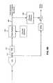
- FIG. 1is a high level block diagram of a DSP-based receiver, in accordance with an aspect of the present invention.
- FIG. 2illustrates an example analog phase interpolator that can be implemented with the digital timing recovery system illustrated in FIG. 10 , in accordance with an aspect of the invention.
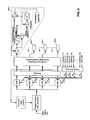
- FIG. 3Ais a block diagram of an example parallel receiver, including an N-path ADC and an M-path DSP, in accordance with an aspect of the invention.
- FIG. 3Bis a more detailed block diagram of an example receiver in accordance with an aspect of the invention.
- FIG. 3Cis a block diagram of individual timing recovery loops that can be implemented for the N ADC paths illustrated in FIG. 3A or 3 B.
- FIG. 3Dillustrates an embodiment where the timing recovery module receives M decisions and M errors from the M DSP paths, in accordance with an aspect of the invention.
- FIG. 3Eillustrates an embodiment where each timing recovery loop includes a phase locked loop and k phase detectors, in accordance with an aspect of the invention.
- FIG. 3Hillustrates an example implementation wherein the timing recovery module includes a decoder and a phase selector/phase interpolator, in accordance with an aspect of the invention.
- FIG. 4Ais a block diagram of an example receiver that utilizes a track and hold device, in accordance with an aspect of the invention.
- FIG. 4Bis a block diagram of an example receiver that utilizes multiple track and hold devices in parallel, in accordance with an aspect of the invention.
- FIG. 5illustrates an example parallel receiver that utilizes, among other things, DFE-based offset cancellation on a per path basis, in accordance with an aspect of the invention.
- FIG. 6illustrates example implementation details of the equalizer illustrated in FIG. 5 , in accordance with an aspect of the present invention.
- FIG. 7illustrates an example programmable gain amplifier and an example automatic gain control module, in accordance with an aspect of the present invention.
- FIG. 8Aillustrates an example implementation for offset mismatch compensation in accordance with an aspect of the present invention.
- FIG. 8Billustrates an example Viterbi decoder-based decision-directed error signal generator, in accordance with an aspect of the invention.
- FIG. 9illustrates another example implementation for offset mismatch compensation, in accordance with an aspect of the present invention.
- FIG. 10is a block diagram of a parallel receiver with independent timing recovery loops for each parallel path, in accordance with an aspect of the invention.
- FIG. 11is a block diagram of an example timing recovery block in accordance with an aspect of the invention.
- FIG. 12illustrates an example analog phase interpolator that can be implemented with the digital timing recovery system illustrated in FIG. 10 , in accordance with an aspect of the invention
- FIG. 13illustrates an example 4-state, 1-step trellis that runs at a clock rate substantially equal to the symbol rate, in accordance with an aspect of the present invention.
- FIG. 14illustrates an example 4-state, M-step trellis that runs at a clock rate substantially equal to 1/M th of the symbol rate, in accordance with an aspect of the present invention.
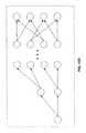
- FIG. 15Aillustrates an example rooted trellis, in accordance with an aspect of the present invention.
- FIG. 15Billustrates another example rooted trellis, in accordance with an aspect of the present invention.
- FIG. 15Cillustrates another example rooted trellis, in accordance with an aspect of the present invention.
- FIG. 15Dillustrates another example rooted trellis, in accordance with an aspect of the present invention.
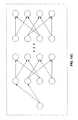
- FIG. 16illustrates an example systolic implementation of rooted trellis computation, in accordance with an aspect the present invention.
- FIG. 17is a high-level block diagram of an example parallel Viterbi processor in accordance with an aspect the present invention.
- FIG. 18is a process flowchart in accordance with an aspect of the invention.
- the present inventionis directed to receivers and, more particularly, to digital signal processing (“DSP”) based receivers, multi-channel receivers, timing recovery schemes, and equalization schemes.
- DSPdigital signal processing
- Various features in accordance with the present inventionare described herein. The various features can generally be implemented alone and/or in various combinations with one another. Example implementations of various combinations of features of the invention are provided herein. The invention is not, however, limited to these examples. Based on the description herein, one skilled in the relevant art(s) will understand that the features described herein can be practiced alone and or in other combinations as well.
- FIG. 1is a high-level block diagram of an example DSP-based receiver 100 , in accordance with the present invention.
- the DSP-based receiver 100receives a data signal 102 through a transmission medium 112 and converts it to a digital data signal 106 .
- the DSP-based receiver 100includes an analog-to-digital converter (“ADC”) 108 that digitizes the data signal 102 and outputs one or more internal digital signals 104 .
- the DSP-based receiver 100also includes a DSP 110 that performs one or more digital signal processes on the one or more digital signals 104 , and outputs one or more digital output signals 106 .
- DSP processes in accordance with the present inventionare described below, which can include, without limitation, equalization, error correction (such as hard or soft decoding of, without limitation, convolutional, trellis, or block codes), timing recovery, automatic gain control, and offset compensation.
- Analog circuitry(not shown in FIG. 1 ) is optionally provided to perform portions of one or more of these functions.
- the ADC 108 and/or the DSP 110are implemented with multiple parallel paths, wherein each parallel path operates at a lower speed relative to the data signal 102 .
- the parallel pathsare operated in an interleaved fashion as described below.
- one or more DSP and/or analog processesincluding, without limitation, one or more processes that compensate for nonidealities in the analog front-end paths, can be performed on a per path basis, as described below.
- the data signal 102is received by the receiver 100 through the transmission medium 112 .
- the data signal 102is typically impaired, due to inter-symbol interference, attenuation, crosstalk, noise, and possibly other impairments. These impairments are typically a function of, among other things, physical properties and the length of the transmission medium 112 . These impairments are said to reduce the “eye opening” of the data signal 102 , making it more difficult to accurately process the data signal 102 .
- the receiver 100includes one or more equalizers (not shown), which may include, without limitation, linear equalizers and/or non-linear equalizers.
- the one or more equalizersimprove the “eye opening” of the data signal 102 .
- the present inventionprovides parallel and non-parallel equalization embodiments.
- FFEfeed forward equalization
- DFEdecision feedback equalization
- equalizationincluding linear and/or non-linear equalization, is performed.
- error correctionsuch as, without limitation, hard or soft decoding of convolutional, trellis, or block codes is implemented in a multi-path receiver.
- Example implementations in accordance with aspects of the inventionare described below. Any of a variety of conventional parallel implementation techniques and/or new techniques in accordance with the invention, or combinations thereof, can be implemented in a parallel multi-path receiver.
- multi-path receiverrefers to a receiver where a single input data signal is digitized by an array of interleaved ADCs and/or processed by a digital signal processor using a parallel implementation, as shown in FIGS. 3A and 3B .
- the receiver 100is implemented as a high speed, or high data rate, DSP-based receiver that receives and digitally processes high data rate data signals 102 .
- High data rate signalsgenerally include data signals in the multi-giga bits per second range.
- a high data rate receiver 100having a high data rate ADC 108 and a high speed DSP 110 , would require one or more high speed (e.g., gigahertz range) clocks.
- high speede.g., gigahertz range
- parallel processingis implemented wherein each parallel path operates at a lower clock rate.
- the N ADCs 312 - 1 through 312 -N and the M DSP paths 314 - 1 through 314 -Moperate at lower data rates than the received data signal 102 . It is important to observe that the DSP paths need not be independent from one another. In other words, there could be cross-connections among the different DSP paths 314 - 1 through 314 -M.
- Other embodimentsuse other values for N, M, and k.
- Motivations to use other values of k, for example k2, include, without limitation, further reducing the clock speed to operate DSP blocks in the receiver. This can be the situation, for example, when implementing complicated algorithms requiring elaborate DSP architectures. In all the examples provided in this disclosure it is assumed that M is larger than or equal to N, therefore k is larger than or equal to one. However, it will be apparent to one skilled in the art that other embodiments where N is larger than M are also possible without departing from the spirit and scope of the present invention. This situation could arise, for example, if high-resolution ADCs were needed.
- the data signal 102is received and digitized into a plurality of N parallel signals 104 - 1 through 104 -N by the array of N lower speed ADCs 312 - 1 through 312 -N.
- the ADCs 312 - 1 through 312 -Ncan be single-bit ADCs or multi-bit ADCs.
- Each of the plurality of digitized parallel signals 104 - 1 through 104 -Ntypically have a sampling rate lower than the symbol rate of the received data signal 102 , but taken together, have a sampling rate substantially the same or higher than the symbol rate of the received data signal 102 .
- the received data signal 102is a high data rate (e.g., gigabit(s) per second range) data signal.
- the modulation schemeis binary (it encodes only one bit per symbol) the symbol rate is substantially equal to the data rate.
- the symbol ratecan be reduced without reducing the data rate by using multilevel modulation schemes such as pulse amplitude modulation (PAM).
- PAMpulse amplitude modulation
- two bits per symbolcould be transmitted by using a 4-level PAM modulation scheme (PAM-4).
- a binary modulation schemeis also known as PAM-2 (other common names are On-Off Keying (OOK) or binary antipodal signaling).
- OOKOn-Off Keying
- the receiverneeds to take at least one sample per symbol of the received signal.
- Baud-rate-sampled receiversare usually called “baud-rate-sampled receivers.” However in some implementations the receiver could take more than one sample per symbol. These receivers are often called “oversampled receivers,” or “fractionally-spaced receivers.” Baud-rate-sampled receivers are usually more economical because, for the same symbol rate, they require lower speed ADCs than oversampled receivers. However, it will be apparent to one skilled in the art that the techniques disclosed in this invention can be applied equally well to baud rate sampled and/or oversampled receivers, as well as to receivers using a variety of modulation schemes, including, but not restricted to, PAM-2, multilevel PAM, single-carrier or multi-carrier quadrature amplitude modulation (QAM), etc.
- PAM-2PAM-2
- QAMquadrature amplitude modulation
- a timing recovery module 318performs timing recovery and provides one or more clock signals 319 to the ADC converter array 108 .
- the timing recovery module 318operates the N lower speed ADCs 312 - 1 through 312 -N in a staggered, or interleaved fashion.
- different phases of the clock signals 319are provided to each of the ADCs 312 - 1 through 312 -N.
- the different phasesare staggered from one another so that each ADC 312 - 1 through 312 -N samples a different portion or phase of the data signal 102 .
- Interleaved samples 104 - 1 through 104 -N from the ADCs 312 - 1 through 312 -Nare aligned by a retiming module 316 . Further signal processing is performed in the M-path DSP 110 .
- the timing recovery module 318outputs a 1250 MHz, eight-phase clock signal 319 on a bus, one phase for each of the ADCs 312 - 1 through 312 -N.
- the eight-phase clock signal 319operates the ADCs 312 - 1 through 312 -N at 1250 MHz, separated in phase from one another by 45 degrees (i.e., 360 degrees/8 phases), in this example.
- a parallel DSP-based receiver in accordance with the inventionis useful for receiving high data rate signals.
- a high data rate DSP-based receiver in accordance with the inventionis useful for lower data rate applications as well.
- the timing recovery module 318includes an individual timing recovery loop for each of the ADC paths defined by the ADCs 312 - 1 through 312 -N. Individual timing recovery loops are described below.
- the example 8-path DSP 110includes an 8-path parallel FFE 320 and an 8-path parallel Viterbi decoder 322 .
- Example implementations of parallel Viterbi decodersare described below. Additional example implementations of the M-path DSP 110 are provided below.
- the present inventionis not, however, limited to these examples. Based on the description herein, one skilled in the relevant art(s) will understand that other N-path ADC and/or M-path DSP configurations are possible.
- the retiming module 316provides samples of the retimed signals to the parallel feedforward equalizer 320 , as well as to the timing recovery module 318 and to the AGC 310 , as illustrated by the dotted lines.
- the receiver 100is illustrated with a programmable gain amplifier 308 and an automatic gain control 310 . Implementation examples and operation of these components are described below.
- a parallel receiver in accordance with the inventionis designed to receive a single data signal.
- a parallel receiver in accordance with the inventionis designed to receive multiple data signals.
- the receiver 100is repeated for each data signal 102 .
- Each repetition of a parallel multi-path DSP-based receiveris referred to herein as a slice, each slice having one or more parallel ADC and/or DSP paths.
- FIG. 4Aillustrates a block diagram of a portion of an example receiver including a track-and-hold device 402 controlled by a clock generator 404 .
- the track and hold device 402provides a constant analog value to the ADC 108 .
- the multi-path receiver 100 illustrated in FIG. 1is implemented with a plurality of track and hold devices.
- FIG. 4Billustrates a block diagram of a portion of an example parallel receiver including an array 408 of parallel track and hold devices 406 - 1 through 406 -N.
- one or more of a variety of types of gain and/or phase errors and interleave path mismatchesare detected and compensated for. Such errors and mismatches can be compensated for on a path-by-path basis and/or on a system wide basis. Compensation design and control considerations for parallel receivers are now described.
- one or more adaptive processesreduce error. Error is used in one or more feedback loops, for example, to generate equalizer coefficients, to optimize ADC sampling phase(s) for timing recovery, and/or to optimize gain for automatic gain control (“AGC”). Error correction can be used for other processes as well.
- ADCautomatic gain control
- Errorcan be computed in one or more of a variety of ways. For example, error can be computed as a difference between input signals and decisions as to the values of the input signals. This is referred to herein as a decision-directed process. Decision-directed processes can be implemented with a slicer. Alternatively, decision-directed processes can be implemented with a Viterbi Decoder, as described below with respect to FIG. 8 . Other decision-directed processes can be used as well. Other error determination processes can also be used.
- Examples provided hereintypically illustrate timing recovery, AGC, and offset cancellation algorithms as decision-directed processes, where error is computed at a slicer or equivalent decision device, such as Viterbi decoder.
- the examplesare provided for illustrative purposes and are not limiting. Based on the teachings herein, one skilled in the relevant art(s) will understand that the techniques can be implemented with non-decision-directed processes as well, and/or in combinations of decision-directed and non-decision-directed processes.
- the multi-phase sampling clock 319 provided by the clock recovery module 318is generated by dividing down a higher frequency clock. Imperfections in the clock dividing circuitry, however, potentially lead to phase differences between the paths that depart from the intended value. This error has a systematic component and a random component.
- the random error componenttends to be approximately similar for the N interleaved ADCs.
- the systematic component of the sampling phase errortends to originate in a divider circuit, typically implemented within a timing recovery module, such as the timing recovery module 318 illustrated in FIG. 3A , and also in mismatches in the propagation delays of the clocks from the timing recovery module to the individual track-and-hold devices (as shown in FIG. 4B , there is a track-and-hold device 406 - 1 through 406 -N in front of each ADC 312 - 1 through 312 -N). Therefore, the sampling instants of the input signal experience a periodic jitter with a fundamental frequency fs, where fs is the frequency of the sampling clock driving each track and hold.
- FIG. 3Cillustrates an example implementation of the timing recovery module 318 including multiple timing recovery loops 318 - 1 through 318 -N.
- Example implementations of the multiple timing recovery loops 318 - 1 through 318 -Nare provided below.
- Timing recovery loopsAn advantage of separate timing recovery loops is that the systematic phase errors introduced in the multi-phase sampling clock 319 by the frequency divider circuit can be independently compensated within the N independent timing recovery loops 318 - 1 through 318 -N. This technique substantially reduces and/or eliminates the systematic component of the phase error in the interleaved ADC converter array 108 , providing increased accuracy and ease of design.
- the systems and methods for compensating sampling phase errors described hereincan be used in combination with one or more of a variety of timing recovery techniques.
- the DSP-based receiver 100utilizes one or more decision-directed timing recovery processes.
- FIG. 3Dillustrates an embodiment where the timing recovery module 318 receives M decisions 324 and M errors 326 from the M DSP paths. The significance and use of the decisions 324 and errors 326 are described below.
- FIG. 3Eillustrates an embodiment where each timing recovery loop 318 - 1 through 318 -N includes a phase locked loop (PLL) 332 and k phase detectors 330 .
- PLLphase locked loop
- Example implementations of the phase locked loop 332 and k phase detectors 330are described below with respect to FIG. 11 .
- FIG. 3Hillustrates an example implementation wherein the timing recovery module 318 includes a decoder 340 and a phase selector/phase interpolator 342 .
- the phase selector/phase interpolator 342receives P phases 344 - 1 through 344 -P, where P is an integer, from a clock generator.
- the phase selector/phase interpolator 342also receives N phase interpolator control signals 346 - 1 through 346 -N from the decoder 340 .
- the phase selector/phase interpolator 342receives the N phase interpolator control signals 346 - 1 through 346 -N directly from the timing recovery loops 318 - 1 through 318 -N.
- the phase selector/phase interpolator 342outputs N phases 319 - 1 through 319 -N.
- Pdoes not necessarily equal N.
- the inventionis not, however, limited to these examples. Based on the description herein, one skilled in the relevant art(s) will understand that other values for N and P can be used.
- Example implementations of the phase selector/phase interpolator 342are described below with respect to FIGS. 2 and 12 .
- FIG. 10illustrates an example implementation of the timing recovery loops 318 - 1 through 318 N wherein each timing recovery loop 318 - 1 through 318 -N receives a decision from a corresponding DSP path and a sample of the slicer error from an adjacent DSP path. This configuration is described below with respect to FIG. 11 .
- Each timing recovery loop 318 - 1 through 318 Nis designed to drive its associated path phase error towards zero.
- the M-path DSP 110includes an FFE 1004 , a DFE 1006 , and slicers 1002 - 1 through 1002 -M. Decisions and slicer error signals are shown as being taken from slicers 1002 - 1 through 1002 -M. Phase error signals are computed by the timing recovery modules 318 - 1 through 318 N, based on the decisions and the slicer errors, as shown in more detail in FIG. 11 . This corresponds to an exemplary decision-directed timing recovery algorithm. However, other timing recovery algorithms can be utilized.
- decisionsare generated from slicers 1002 , and errors are generated as a difference between the slicer decisions and the input to the slicers 1002 .
- decisions and errorsare generated with a Viterbi decoder and channel estimator.
- a Viterbi decoder 804receives an input signal 810 through a feed-forward equalizer 812 , and outputs decisions 806 , which can be final decisions or tentative decisions.
- Tentative decisionscan be provided by the Viterbi decoder 804 with less delay than final decisions, while final decisions tend to be more accurate than tentative decisions.
- the choice between tentative decisions and final decisionsis generally a trade-off between latency and accuracy.
- the choicecan be influenced by the quality of the input signal 810 .
- the decisions 806are provided to a channel estimator 808 , the output of which is subtracted from the input signal 810 .
- the resulting erroris analogous to the slicer error described above.
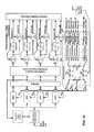
- FIG. 11is a block diagram of an example implementation of the timing recovery loop 318 - 1 illustrated in FIGS. 3C-3H and FIG. 10 .
- Timing recovery loops 318 - 2 through 318 -Nare similarly configured.
- the timing recovery loop 318 - 1includes k phase detectors 1104 - 1 through 1104 - k , which generate k phase error signals 1106 - 1 through 1106 - k .
- Each phase error signal 1106 - 1 through 1106 - kis generated by cross-correlating a decision 1110 for a given path with a slicer error 1108 corresponding to an adjacent path, as illustrated in FIGS. 3F and 3G , for example
- the phase error signals 1106 - 1 through 1106 - kare computed in the exemplary embodiment of FIG. 11 , by, for example, using a variety of the well-known Mueller and Muller algorithms. See, for example, K. H. Mueller and M. Muller, “Timing Recovery in Digital Synchronous Data Receivers,” IEEE Transactions on Communications COM-24, pp. 516-531, May 1976, incorporated herein by reference in its entirety, where the phase error is based on the precursor of the channel impulse response at the output of the FFE, with the precursor taken one symbol period before the sample on which the decision is based. In this algorithm, the phase error is computed with the slicer error delayed by one symbol period.
- the one symbol delay of the erroris achieved by, for example, taking the error sample from an adjacent path, as shown in FIG. 10 .
- the decision 1110comes from the same path where phase is being controlled, but the error 1108 comes from the adjacent path corresponding to the samples of the input signal taken one baud period earlier. Because of the parallel architecture of the DSP, these samples appear at the same cycle of the DSP clock, but on an adjacent path.
- a delay 350is inserted in the error 1108 - 1 because the error M 1108 - 1 comes from a preceding block relative to the decision 1110 - 1 .
- the delay 350is substantially equal to M cycles of the input or baud clock, or one cycle of the DSP clock. For example, where the data signal 102 is a 10 Gbit/sec signal, and where M equals 4 (i.e., 4 DSP paths), the delay 350 is set to 1 ⁇ 4 of 10 Gbits/sec., or approximately 400 picoseconds.
- phase error signals 1106 - 1 through 1106 - kare filtered by an accumulate and dump filter 1112 and further filtered by an integral filter 1118 .
- the sum of the proportional and integral pathsis used to control a numerically controlled oscillator (“NCO”) 1114 . Therefore, the phase locked loop illustrated by FIG. 11 is a second-order (or proportional plus integral) loop.
- Digital control words 1116 generated by the NCO 1114are used to control a phase selector (not shown in FIG. 11 ).
- phase compensationis performed with a phase interpolator or phase selector.
- the phase selectordigitally generates multi-phase sampling clocks by, for example, taking a weighted sum of multiple (e.g., 4), phases with finite rise and fall times.
- FIGS. 2 and 12illustrate example phase selectors in accordance with aspects of the invention.
- the example phase selector in FIG. 2generally provides faster response times.
- a conventional phase selectoris utilized.
- the present inventionis not, however, limited to digitally controlled phase selectors.
- FIG. 2illustrates an example phase selector 202 in accordance with an aspect of the invention.
- the phase selector 202 shown in FIG. 2exemplifies a situation where the number of output phases fs 1 through fs N may be different from the number of input phases f′s 1 through f′s p .
- the number of output phases fs 1 through fs Nis always N, the same as the number of ADC paths.
- the number P of input phases f′s 1 through f′s pcould be smaller than N.
- Nis a multiple of P.
- the phase selector 202includes N interpolator sub-blocks 202 - 1 through 202 -N, that receive digital control words C 1 through C N , respectively.
- the digital control words C 1 through C Ncorrespond to the phase interpolator control signals 346 - 1 through 346 -N described above with respect to FIG. 3H .
- phase interpolator sub-block 202 - 1is illustrated in detail, operation of which is now described.
- the digital control word C 1is applied through a decoder to current-mode digital-to-analog converters (“DACs”) 204 - 1 through 204 -P, which control the bias current of respective differential pairs 208 - 1 through 208 -P.
- DACsdigital-to-analog converters
- the inputs to the differential pairs 208 - 1 through 208 -Pare taken from consecutive input phases.
- the drain currents of the differential pairs 208 - 1 through 208 -Pare combined in output resistors 212 and 214 , which generate the output phase fs 1
- the output phase fs 1is thus a weighted sum of f′s 1 through f′s p , wherein the weighting is determined by the DACs 204 - 1 through 204 -P, under control of the control signal C 1 .
- phase interpolator sub-blocks 202 - 1 through 202 -Neach one corresponding to an output phase.
- the number of input phases Pis typically smaller than the number of output phases, N.
- Nthe number of output phases
- the essential aspect of this phase selector 202is the use of digitally controlled weighted sums of two input phases to generate an output phase. This concept can be implemented in many alternative ways without departing from the spirit and scope of the present invention, as will be apparent to one skilled in the art.
- multi-phase sampling clocks 319are generated by a resistive phase interpolator.
- FIG. 12illustrates an example timing recovery block 1202 implementation, which is an example embodiment of the timing recovery block 318 illustrated in FIG. 10 .
- the timing recovery block 1202includes a resistive interpolation ring phase selector 1204 .
- Input phases f′s 1-N 1206 from a clock generatorare provided to the resistive interpolation ring phase selector 1204 .
- the input phases f′s 1-N 1206are derived from a divider operating on an independent clock. When the frequency of operation of the divided down clock is relatively high, the clock edges tend to have finite rise and fall times that are comparable to the period of the waveform.
- the number of input phases Pneed not be the same as the number of ADC paths N. This is explained more clearly in connection with FIG. 2 .
- phase differenceis electrically controlled by changing the relative interpolation factors by, for example, changing the values of the interpolation resistors in a digital fashion, driven by, for example, the timing recovery circuit.
- phase selector implementations described hereinare provided for illustrative purposes. The present invention is not limited to these examples. Based on the teachings herein, one skilled in the relevant art(s) will understand that other phase selector methods and systems can be utilized.
- methods and systemsare provided for reducing gain errors, offsets, and/or undesired sampling clock phase differences among the paths defined by the ADCs 312 - 1 through 312 -N ( FIG. 3A ).
- gain and offset mismatches between pathsare compensated for in a DSP, wherein gain factors adapt for individual paths.
- FIG. 5illustrates an example DSP-based parallel receiver 500 , which is an example implementation of the receiver 100 illustrated in FIG. 3A .
- the receiver 500utilizes DFE-based offset cancellation on a per path basis, in accordance with an aspect of the invention.
- offsets originating in the ADC 108 or anywhere in the analog front endare individually controlled for each ADC path by an equalizer adaptation algorithm to compensate the offsets in the digital domain independently for each path.
- a single Programmable Gain Amplifier 308 with global gain controlis shown.
- independent gain control for each ADC pathcan also be implemented in the digital domain using, for example, Feed-forward Equalizer.
- FFE-based digital controlcan be omitted where, for example, the gain errors of the ADC paths can be accurately controlled by design, thus requiring little or no digital gain mismatch compensation. In a more common situation, relatively significant gain mismatches exist among the ADC paths, therefore digital compensation of gain mismatches is preferred.
- a scheme where gain mismatches in the ADC paths are individually compensated in the analog domainwill be discussed later in connection with FIG. 7 .
- gain mismatchescan be digitally compensated using the Feed-forward Equalizer.
- FIG. 5also shows the independent phase error compensation technique already discussed in connection with FIGS. 10 , 11 , and 12 .
- sampling phase error, gain error, and offset compensation techniques disclosed hereincan be used independently of each other and in any combination required, depending on the need for compensation of the different errors that circuit design and/or manufacturing tolerance considerations motivate in each specific situation.
- the M-path DSP 110includes an M-path parallel FFE 508 , M individual decision and error paths, and an M-path DFE 510 .
- the number of parallel ADC paths Nequals the number of parallel DSP paths M. The invention is not, however, limited to this embodiment.
- the example parallel receiver 500shows an implementation of a DFE and offset cancellation scheme that can not only compensate for offset, but can also compensate for offset mismatches among the interleaved array of ADC paths.
- the offset cancellation schemeis implemented with one or more DC taps per ADC path in the DFE 510 .
- FIG. 9where the DC taps are implemented by the integrators inside blocks 902 - 1 through 902 -M.
- FIG. 8also uses DC taps in the DFE to compensate for offsets independently for each ADC path, but in this case compensation is done in the analog domain. Since each interleave uses an independent, and independently adapted, DC tap, offsets that do not necessarily match across the interleaved paths can be compensated.
- the timing recovery module 318receives decisions and errors from the M individual decision and error paths in the DSP 110 , and adjusts the phases of the sampling clocks 319 - 1 through 319 -N accordingly.
- gain factorsare individually controlled for each path after the ADC array 108 .
- Overall dynamic range of the ADC converter array 108is optionally controlled by the AGC module 310 and the PGA module 308 . This helps to optimize use of all of the bits of the ADC array 108 .
- FIG. 6illustrates an example of a 4-tap adaptive FFE 508 implemented as a 4-parallel array having paths 602 - 1 through 602 - 4 .
- the number of taps and the degree of parallelizationcan be varied as desired.
- the parallel paths 602 - 1 through 602 - 4are essentially four adaptive transversal filters.
- the FFEcan also act as an interpolation filter. Having independent coefficients for the different parallel sections, as explained before, means that the FFE can also compensate for sampling phase errors in the ADCs. This is particularly true when the input signal is bandlimited to half the baud rate or less. This provides an alternative way to compensate for sampling phase errors, as well as gain errors in the ADCs of an interleaved array.
- FIG. 7illustrates an example path-specific AGC implementation, which can be utilized to reduce gain errors in the interleaved paths.
- the example path specific AGC implementation illustrated in FIG. 7can be implemented in place of the FFE-based gain error compensation scheme illustrated in FIGS. 5 and 6 . It can also be combined with offset compensation schemes like the ones discussed in connection with FIGS. 5 and 8 .
- FIG. 7illustrates an implementation of a portion 700 of the receiver 100 illustrated in FIG. 3A , in accordance with an aspect of the invention.
- the portion 700includes a plurality of path-specific AGCs 310 - 1 through 310 -N, which control a PGA array of path-specific PGAs 308 - 1 through 308 -N.
- Path-specific AGCs 310 - 1 through 310 -Nare now described with reference to path-specific AGC 310 - 1 .
- Path-specific AGCs 310 - 2 through 310 -Nare configured similarly.
- Path-specific AGC 310 - 1includes an absolute value module 704 - 1 and a lowpass filter 706 - 1 , which provides a measured amplitude 708 - 1 to a differencer 726 - 1 .
- the differencer 726 - 1subtracts a desired amplitude 712 - 1 from the measured amplitude 708 - 1 and outputs a difference value 714 - 1 to an adder 716 - 1 .
- the adder 716 - 1 together with the accumulator 722 - 1constitute a digital integrator.
- the integratorintegrates the difference value 714 - 1 and outputs a PGA control value 724 - 1 to PGA 308 - 1 .
- PGA control value 724 - 1is optionally provided to ADC 312 - 1 to adjust a reference voltage therein.
- Path-specific AGCs 310 - 2 through 310 -Noperate in a similar fashion.
- gain errorsare obtained or generated in the digital domain, and used to control the independent PGAs 308 - 1 through 308 -N. Since the gain error is measured in the digital domain, any gain errors introduced by the lower frequency ADCs 312 - 1 through 312 -N will be driven to approximately zero by the AGC circuitry.
- automatic gain controlcan be implemented in other ways. For example, and without limitation, where gain mismatches of the interleaved ADC paths are relatively negligible, automatic gain control can be shared by all of the ADC paths, wherein the PGAs 308 - 1 through 308 -N share a common control signal.
- FIG. 8illustrates an example implementation for gain and offset mismatch compensation, where offset associated with each ADC 312 - 1 through 312 -N in the interleaved ADC array 108 is substantially cancelled in the analog domain.
- Analog cancellationcan be utilized in place of, or in addition to digital cancellation. Offsets introduced by each of the lower frequency ADCs 312 - 1 through 312 -N are preferably measured in the digital domain. Alternatively, offsets introduced by each of the lower frequency ADCs 312 - 1 through 312 -N are measured in the analog domain.
- the gain errorscan be compensated for by controlling the reference voltage of the ADCs.
- the PGAcan be shared across all the interleaves.
- FIG. 9illustrates an exemplary receiver implementation that compensates offset mismatches.
- the exemplary implementationcan be further modified to compensate gain errors between the ADC paths as well. Based on the description herein, one skilled in the relevant art(s) will understand that the exemplary implementation illustrated in FIG. 9 can be modified in a variety of ways to compensate for gain errors.
- one or more types of equalizationare performed in a parallel multi-path receiver.
- Viterbi equalizationis performed in a multi-path receiver.
- the inventionis not, however, limited to this example.
- the amount of hardware needed for the parallel implementationgenerally grows linearly with the degree of parallelization M. This allows large parallelization factors M to be implemented, and makes implementation of Viterbi decoders feasible at relatively high symbol rates.
- Parallelizationis based on the idea of defining an M-step trellis (also with S states), which represents the state transitions after M symbol periods.
- Branch metrics for the M-step trelliscan be computed using S “rooted trellises.” Computation of the rooted trellises can be parallelized.
- FIG. 13illustrates an example 4-state, 1-step trellis 1300 that runs at a clock rate substantially equal to the symbol rate, in accordance with an aspect of the present invention.
- FIG. 14illustrates an example 4-state, M-step trellis 1400 that runs at a clock rate substantially equal to 1/M th of the symbol rate, in accordance with an aspect of the present invention.
- FIGS. 15A through 15Dillustrate example rooted trellises, in accordance with aspects of the present invention.
- FIG. 16illustrates an example systolic implementation of rooted trellis computation, in accordance with an aspect the present invention.
- FIG. 17is a high level block diagram of an example parallel Viterbi processor in accordance with an aspect the present invention.
- the inventionincludes error correction processing. This processing can be done by the Viterbi decoder or elsewhere. Error correction processing includes, but is not limited to, hard-decision decoding or soft-decision decoding of convolutional, trellis, or block codes.
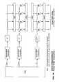
- FIG. 18illustrates a process flowchart 1800 for implementing the present invention.
- the process flowchart 1800is described below with reference to one or more of the example system implementations illustrated in one or more of the drawing FIGS. 1-17 .
- the present inventionis not, however, limited to the example system implementations illustrated in drawing FIGS. 1-17 .
- the process flowchart 1800can be implemented with other system implementations as well. Such other implementations are within the spirit and scope of the present invention.
- step 1802which includes receiving a data signal having a symbol rate.
- a data signal 102is received through transmission medium 112 .
- Step 1804includes generating N sampling signals having a frequency that is lower than the symbol rate, the N sampling signals shifted in phase relative to one another.
- FIG. 3Aillustrates a timing recovery module 318 , which generates N timing control signals 319 - 1 through 319 -N, as illustrated in FIG. 3C .
- the timing control signals 319 - 1 through 319 -Nhave a lower frequency than the symbol rate of the received signal, and are staggered in phase from one another, as described above.
- Step 1806includes controlling N analog-to-digital converter (“ADC”) paths with the N sampling signals to sample the data signal at the phases. This is described above, for example, with respect to FIG. 3A .
- ADCanalog-to-digital converter
- Step 1808includes individually adjusting one or more parameters for each of the N ADC paths.
- Step 1810can include, without limitation, individually adjusting each of the N sampling signals to reduce sampling phase errors in the N ADC paths, individually adjusting for offsets in the N ADC paths, and/or individually adjusting for gain errors in said N ADC paths.
- Step 1810includes generating a digital signal representative of the received data signal from samples received from the N ADC paths. In FIG. 1 , this is illustrated by the output digital signal(s) 106 .
- Steps 1802 through 1810are illustrated as discrete sequential steps for illustrative purposes. Steps 1802 through 1810 are not, however, limited to performance in discrete sequential steps. In practice, one or more of steps 1802 through 1810 are typically performed in other sequences, and/or using feedback from the same step, and/or using input and/or feedback from one or more other steps.
Landscapes
- Engineering & Computer Science (AREA)
- Computer Networks & Wireless Communication (AREA)
- Signal Processing (AREA)
- Power Engineering (AREA)
- Physics & Mathematics (AREA)
- Electromagnetism (AREA)
- Theoretical Computer Science (AREA)
- Dc Digital Transmission (AREA)
- Error Detection And Correction (AREA)
- Cable Transmission Systems, Equalization Of Radio And Reduction Of Echo (AREA)
- Analogue/Digital Conversion (AREA)
Abstract
Description
Claims (26)
Priority Applications (2)
| Application Number | Priority Date | Filing Date | Title |
|---|---|---|---|
| US11/826,414US7778286B2 (en) | 2000-07-21 | 2007-07-16 | Methods and systems for DSP-based receivers |
| US12/805,712US8363683B2 (en) | 2000-07-21 | 2010-08-16 | Methods and systems for DSP-based receivers |
Applications Claiming Priority (5)
| Application Number | Priority Date | Filing Date | Title |
|---|---|---|---|
| US21991800P | 2000-07-21 | 2000-07-21 | |
| US27321501P | 2001-03-01 | 2001-03-01 | |
| US09/909,896US7564866B2 (en) | 2000-07-21 | 2001-07-23 | Methods and systems for digitally processing optical data signals |
| US10/085,071US7245638B2 (en) | 2000-07-21 | 2002-03-01 | Methods and systems for DSP-based receivers |
| US11/826,414US7778286B2 (en) | 2000-07-21 | 2007-07-16 | Methods and systems for DSP-based receivers |
Related Parent Applications (2)
| Application Number | Title | Priority Date | Filing Date |
|---|---|---|---|
| US09/909,896Continuation-In-PartUS7564866B2 (en) | 2000-07-21 | 2001-07-23 | Methods and systems for digitally processing optical data signals |
| US10/085,071ContinuationUS7245638B2 (en) | 2000-07-21 | 2002-03-01 | Methods and systems for DSP-based receivers |
Related Child Applications (1)
| Application Number | Title | Priority Date | Filing Date |
|---|---|---|---|
| US12/805,712ContinuationUS8363683B2 (en) | 2000-07-21 | 2010-08-16 | Methods and systems for DSP-based receivers |
Publications (2)
| Publication Number | Publication Date |
|---|---|
| US20070263673A1 US20070263673A1 (en) | 2007-11-15 |
| US7778286B2true US7778286B2 (en) | 2010-08-17 |
Family
ID=38685070
Family Applications (3)
| Application Number | Title | Priority Date | Filing Date |
|---|---|---|---|
| US10/085,071Expired - Fee RelatedUS7245638B2 (en) | 2000-07-21 | 2002-03-01 | Methods and systems for DSP-based receivers |
| US11/826,414Expired - Fee RelatedUS7778286B2 (en) | 2000-07-21 | 2007-07-16 | Methods and systems for DSP-based receivers |
| US12/805,712Expired - Fee RelatedUS8363683B2 (en) | 2000-07-21 | 2010-08-16 | Methods and systems for DSP-based receivers |
Family Applications Before (1)
| Application Number | Title | Priority Date | Filing Date |
|---|---|---|---|
| US10/085,071Expired - Fee RelatedUS7245638B2 (en) | 2000-07-21 | 2002-03-01 | Methods and systems for DSP-based receivers |
Family Applications After (1)
| Application Number | Title | Priority Date | Filing Date |
|---|---|---|---|
| US12/805,712Expired - Fee RelatedUS8363683B2 (en) | 2000-07-21 | 2010-08-16 | Methods and systems for DSP-based receivers |
Country Status (1)
| Country | Link |
|---|---|
| US (3) | US7245638B2 (en) |
Cited By (8)
| Publication number | Priority date | Publication date | Assignee | Title |
|---|---|---|---|---|
| US20090167402A1 (en)* | 2007-12-31 | 2009-07-02 | Kathy Tian | Dual barrel receiver equalization architecture |
| US20110304489A1 (en)* | 2010-06-15 | 2011-12-15 | Zoran Corporation | Methods of and arrangements for offset compensation of an analog-to-digital converter |
| US8478554B1 (en)* | 2009-02-09 | 2013-07-02 | Marvell International Ltd. | Reducing eye monitor data samplers in a receiver |
| US20140133603A1 (en)* | 2007-04-30 | 2014-05-15 | Scott R. Velazquez | Adaptive digital receiver |
| US8971468B1 (en)* | 2013-10-28 | 2015-03-03 | Xilinx, Inc. | Increasing the resolution of serial data recovery units (DRUs) based on interleaved free running oversamplers |
| US11177986B1 (en)* | 2020-11-24 | 2021-11-16 | Texas Instruments Incorporated | Lane adaptation in high-speed serial links |
| US11223468B1 (en)* | 2020-08-18 | 2022-01-11 | Samsung Electronics Co., Ltd. | Receiver circuit performing adaptive equalization and system including the same |
| US20240372561A1 (en)* | 2023-05-04 | 2024-11-07 | National Tsing Hua University | Decoder for decoding data in a pam-2m format, decoder device using the decoder, and receiver using the decoder device |
Families Citing this family (99)
| Publication number | Priority date | Publication date | Assignee | Title |
|---|---|---|---|---|
| US7058150B2 (en) | 2000-04-28 | 2006-06-06 | Broadcom Corporation | High-speed serial data transceiver and related methods |
| US7319719B1 (en)* | 2000-06-21 | 2008-01-15 | Adc Telecommunications, Inc. | Parallel equalization for systems using time division multiple access |
| US7245638B2 (en)* | 2000-07-21 | 2007-07-17 | Broadcom Corporation | Methods and systems for DSP-based receivers |
| US7564866B2 (en)* | 2000-07-21 | 2009-07-21 | Broadcom Corporation | Methods and systems for digitally processing optical data signals |
| US7486894B2 (en) | 2002-06-25 | 2009-02-03 | Finisar Corporation | Transceiver module and integrated circuit with dual eye openers |
| US7809275B2 (en)* | 2002-06-25 | 2010-10-05 | Finisar Corporation | XFP transceiver with 8.5G CDR bypass |
| US7561855B2 (en)* | 2002-06-25 | 2009-07-14 | Finisar Corporation | Transceiver module and integrated circuit with clock and data recovery clock diplexing |
| US7664401B2 (en)* | 2002-06-25 | 2010-02-16 | Finisar Corporation | Apparatus, system and methods for modifying operating characteristics of optoelectronic devices |
| US7437079B1 (en) | 2002-06-25 | 2008-10-14 | Finisar Corporation | Automatic selection of data rate for optoelectronic devices |
| US7477847B2 (en)* | 2002-09-13 | 2009-01-13 | Finisar Corporation | Optical and electrical channel feedback in optical transceiver module |
| JP3486186B1 (en)* | 2002-10-23 | 2004-01-13 | 沖電気工業株式会社 | Received data playback device |
| US20040218705A1 (en)* | 2003-01-30 | 2004-11-04 | International Business Machines Corporation | Phase rotator, phase rotation method and clock and data recovery receiver incorporating said phase rotator |
| US7292662B2 (en)* | 2003-03-26 | 2007-11-06 | Infineon Technologies Ag | Feed forward clock and data recovery unit |
| US7457391B2 (en)* | 2003-03-26 | 2008-11-25 | Infineon Technologies Ag | Clock and data recovery unit |
| US7206363B2 (en) | 2003-06-24 | 2007-04-17 | Intersymbol Communications, Inc. | Method and apparatus for delayed recursion decoder |
| EP1494413A1 (en)* | 2003-07-02 | 2005-01-05 | CoreOptics, Inc., c/o The Corporation Trust Center | Channel estimation and sequence estimation for the reception of optical signal |
| US7227508B2 (en)* | 2004-01-07 | 2007-06-05 | Motia Inc. | Vehicle mounted satellite antenna embedded within moonroof or sunroof |
| US7522901B2 (en)* | 2004-01-20 | 2009-04-21 | Broadcom Corporation | Direct digital conversion tuner and method for using same |
| US8732788B2 (en)* | 2004-05-21 | 2014-05-20 | Broadcom Corporation | Integrated set-top box |
| US8578434B2 (en) | 2004-05-21 | 2013-11-05 | Broadcom Corporation | Integrated cable modem |
| US7961823B2 (en)* | 2004-06-02 | 2011-06-14 | Broadcom Corporation | System and method for adjusting multiple control loops using common criteria |
| US8239914B2 (en)* | 2004-07-22 | 2012-08-07 | Broadcom Corporation | Highly integrated single chip set-top box |
| DE102004049161B4 (en)* | 2004-10-08 | 2009-10-29 | Infineon Technologies Ag | Time-shifted analog-to-digital converter |
| KR100689039B1 (en)* | 2005-02-01 | 2007-03-09 | 삼성전자주식회사 | Analog Viterbi decoder using cyclic decoding unit in parallel |
| KR100674953B1 (en)* | 2005-02-05 | 2007-01-26 | 학교법인 포항공과대학교 | Equalization Receiver of Semiconductor Memory |
| US7602127B2 (en) | 2005-04-18 | 2009-10-13 | Mks Instruments, Inc. | Phase and frequency control of a radio frequency generator from an external source |
| US8102954B2 (en)* | 2005-04-26 | 2012-01-24 | Mks Instruments, Inc. | Frequency interference detection and correction |
| CN100579146C (en)* | 2005-09-02 | 2010-01-06 | 深圳市东进通讯技术股份有限公司 | Module configuration management method in integrated telecommunication platform |
| US8831074B2 (en) | 2005-10-03 | 2014-09-09 | Clariphy Communications, Inc. | High-speed receiver architecture |
| US8139630B2 (en)* | 2005-10-03 | 2012-03-20 | Clariphy Communications, Inc. | High-speed receiver architecture |
| US7852913B2 (en)* | 2005-10-03 | 2010-12-14 | Clariphy Communications, Inc. | High-speed receiver architecture |
| FR2896109B1 (en)* | 2006-01-06 | 2008-06-20 | Thales Sa | DIGITAL ANALOGUE CONVERSION DEVICE WITH TEMPORARY INTERLACING AND ADAPTIVE AUTO EQUALIZATION. |
| US8094056B2 (en)* | 2006-02-02 | 2012-01-10 | Clariphy Communications, Inc. | Analog-to-digital converter |
| US7454658B1 (en)* | 2006-02-10 | 2008-11-18 | Xilinx, Inc. | In-system signal analysis using a programmable logic device |
| US7650248B1 (en) | 2006-02-10 | 2010-01-19 | Xilinx, Inc. | Integrated circuit for in-system signal monitoring |
| JP2008011189A (en)* | 2006-06-29 | 2008-01-17 | Nec Electronics Corp | Time interleave a/d conversion apparatus |
| US8441751B1 (en)* | 2006-08-18 | 2013-05-14 | Marvell International Ltd. | Dibit pulse extraction methods and systems |
| US8441752B1 (en)* | 2006-08-30 | 2013-05-14 | Marvell International Ltd. | Dibit pulse extraction methods and systems |
| JP4574658B2 (en)* | 2006-12-13 | 2010-11-04 | パナソニック株式会社 | Wireless device |
| US7688237B2 (en)* | 2006-12-21 | 2010-03-30 | Broadcom Corporation | Apparatus and method for analog-to-digital converter calibration |
| US8238500B2 (en) | 2007-10-02 | 2012-08-07 | Seagate Technology Llc | Channel architecture with multiple signal processing branches for a given physical channel |
| US8331898B2 (en)* | 2007-10-03 | 2012-12-11 | Texas Instruments Incorporated | Power-saving receiver circuits, systems and processes |
| US8004335B2 (en)* | 2008-02-11 | 2011-08-23 | International Business Machines Corporation | Phase interpolator system and associated methods |
| WO2009114738A2 (en)* | 2008-03-12 | 2009-09-17 | Hypres, Inc. | Digital radio-frequency tranceiver system and method |
| US8102938B2 (en)* | 2008-04-22 | 2012-01-24 | Finisar Corporation | Tuning system and method using a simulated bit error rate for use in an electronic dispersion compensator |
| US7714760B2 (en)* | 2008-06-27 | 2010-05-11 | Entropic Communications, Inc. | Apparatus and methods for direct quadrature sampling |
| US8358729B2 (en)* | 2008-08-22 | 2013-01-22 | Finisar Corporation | Baseband phase-locked loop |
| JP5338206B2 (en)* | 2008-08-29 | 2013-11-13 | 富士通株式会社 | Control device, polarization multiplexed optical modulator, optical transmitter, and polarization multiplexed optical modulator control method |
| US20100306814A1 (en)* | 2009-05-26 | 2010-12-02 | Broadcom Corporation | Integrated Set-Top Box with Daisy-Chaining |
| JP5407595B2 (en)* | 2009-06-30 | 2014-02-05 | 富士通株式会社 | Signal processing circuit, optical receiver, detector, and waveform distortion compensation method |
| WO2011091527A1 (en)* | 2010-02-01 | 2011-08-04 | Kapik Inc | System and method for digitally correcting mismatches in multipath adcs |
| US8498217B2 (en)* | 2010-07-01 | 2013-07-30 | Broadcom Corporation | Method and system for adaptive tone cancellation for mitigating the effects of electromagnetic interference |
| KR101423111B1 (en)* | 2010-08-10 | 2014-07-30 | 창원대학교 산학협력단 | Band pass sampling receiver |
| JP5742556B2 (en)* | 2011-07-29 | 2015-07-01 | 富士通セミコンダクター株式会社 | ADC |
| US8879616B2 (en)* | 2011-10-31 | 2014-11-04 | Hewlett-Packard Development Company, L.P. | Receiver with decision feedback equalizer |
| US8537044B2 (en)* | 2011-12-28 | 2013-09-17 | Guzik Technical Enterprises | Interleaved analog to digital converter with digital equalization |
| US8520968B1 (en)* | 2012-02-23 | 2013-08-27 | Telefonaktiebolaget L M Ericsson (Publ) | Communication signal image suppression for multi-frequency operation |
| CN103326722B (en)* | 2012-03-19 | 2017-11-24 | 深圳市中兴微电子技术有限公司 | A kind of adaptive sample value estimating circuit and method |
| US20130285720A1 (en)* | 2012-04-26 | 2013-10-31 | Rafel Jibry | Multiple channel phase detection |
| US8958501B2 (en)* | 2012-11-26 | 2015-02-17 | Broadcom Corporation | Quasi-digital receiver for high speed SER-DES |
| US9385858B2 (en)* | 2013-02-20 | 2016-07-05 | Avago Technologies General Ip (Singapore) Pte. Ltd. | Timing phase estimation for clock and data recovery |
| US9825785B2 (en)* | 2014-03-03 | 2017-11-21 | Multiphy Ltd. | Enhanced equalization based on a combination of reduced complexity MLSE and linear equalizer for heavily ISI-induced signals |
| US9444515B2 (en)* | 2014-04-25 | 2016-09-13 | The Regents Of The University Of Michigan | Short-range zigbee compatible receiver with near-threshold digital baseband |
| US9432126B1 (en)* | 2014-06-25 | 2016-08-30 | Rockwell Collins, Inc. | Reconfigurable filter |
| US9503116B2 (en) | 2014-12-17 | 2016-11-22 | Analog Devices, Inc. | Efficient calibration of errors in multi-stage analog-to-digital converter |
| US9270291B1 (en)* | 2015-01-13 | 2016-02-23 | Broadcom Corporation | High speed time-interleaved ADC gain offset and skew mitigation |
| US20160218734A1 (en)* | 2015-01-23 | 2016-07-28 | Avago Technologies General Ip (Singapore) Pte. Ltd. | Dual threshold automatic gain control system and method |
| KR102222449B1 (en)* | 2015-02-16 | 2021-03-03 | 삼성전자주식회사 | Tap Embedded Data Receiver and Data Transmission System Having The Same |
| CN104679682B (en)* | 2015-03-18 | 2017-12-01 | 四川特伦特科技股份有限公司 | Communication board based on high-speed dsp |
| CN104702287B (en)* | 2015-03-18 | 2017-12-01 | 四川特伦特科技股份有限公司 | A kind of high speed analog-digital conversion process circuit |
| CN104679683B (en)* | 2015-03-20 | 2018-01-05 | 四川特伦特科技股份有限公司 | A kind of DSP process plates with remote control open function |
| CN104967465B (en)* | 2015-07-03 | 2017-10-24 | 桂林电子科技大学 | The digital frequency-adjustable impulse radio ultra-wideband emitters of CMOS |
| DE102015217435A1 (en)* | 2015-09-11 | 2017-03-16 | Robert Bosch Gmbh | Integrated circuit |
| US10263663B2 (en)* | 2015-12-17 | 2019-04-16 | Intel Corporation | M-ary pulse amplitude modulation digital equalizer |
| US9602116B1 (en)* | 2016-01-07 | 2017-03-21 | Inphi Corporation | Interleaved successive approximation register analog to digital converter |
| US9853807B2 (en)* | 2016-04-21 | 2017-12-26 | Taiwan Semiconductor Manufacturing Co., Ltd. | Automatic detection of change in PLL locking trend |
| CN107864017B (en)* | 2016-09-22 | 2019-10-18 | 深圳市中兴微电子技术有限公司 | A phase correction method and device |
| US10305495B2 (en)* | 2016-10-06 | 2019-05-28 | Analog Devices, Inc. | Phase control of clock signal based on feedback |
| US9800438B1 (en)* | 2016-10-25 | 2017-10-24 | Xilinx, Inc. | Built-in eye scan for ADC-based receiver |
| US10153844B2 (en)* | 2017-04-03 | 2018-12-11 | Futurewei Technologies, Inc. | Channel recovery in burst-mode, time-division multiplexing (TDM) passive optical networks (PONs) |
| US10778364B2 (en) | 2017-04-15 | 2020-09-15 | Futurewei Technologies, Inc. | Reduced power consumption for digital signal processing (DSP)-based reception in time-division multiplexing (TDM) passive optical networks (PONs) |
| US10014026B1 (en) | 2017-06-20 | 2018-07-03 | Seagate Technology Llc | Head delay calibration and tracking in MSMR systems |
| US11016681B1 (en) | 2018-07-31 | 2021-05-25 | Seagate Technology Llc | Multi-threshold parameter adaptation |
| US11018842B1 (en) | 2018-07-31 | 2021-05-25 | Seagate Technology Llc | Dynamic timing recovery bandwidth modulation for phase offset mitigation |
| US10803902B1 (en) | 2018-08-19 | 2020-10-13 | Seagate Technology Llc | Hardware-based read sample averaging |
| US10468060B1 (en) | 2018-09-27 | 2019-11-05 | Seagate Technology Llc | Cancelling adjacent track interference |
| EP3686617B1 (en)* | 2019-01-23 | 2025-03-05 | Rohde & Schwarz GmbH & Co. KG | Jitter determination method and measurement instrument |
| US11133787B2 (en) | 2019-06-25 | 2021-09-28 | The Nielsen Company (Us), Llc | Methods and apparatus to determine automated gain control parameters for an automated gain control protocol |
| US11019301B2 (en) | 2019-06-25 | 2021-05-25 | The Nielsen Company (Us), Llc | Methods and apparatus to perform an automated gain control protocol with an amplifier based on historical data corresponding to contextual data |
| US10720936B1 (en)* | 2019-07-22 | 2020-07-21 | eTopus Technology Inc. | ADC reconfiguration for different data rates |
| CN111342841B (en)* | 2020-03-10 | 2023-02-28 | 西南科技大学 | A reconfigurable multi-channel signal acquisition and transmission system |
| US11658696B2 (en)* | 2021-03-17 | 2023-05-23 | Microsoft Technology Licensing, Llc | Network transceiver with VGA channel specific equalization |
| KR102845458B1 (en)* | 2021-04-14 | 2025-08-11 | 삼성전자주식회사 | An Analog-to-Digital conversion circuit and receiver including the same |
| EP4324096A4 (en)* | 2021-05-11 | 2024-06-12 | Huawei Technologies Co., Ltd. | Modulo-based analog-to-digital conversion apparatus and method |
| US11381269B1 (en) | 2021-05-28 | 2022-07-05 | Marvell Asia Pte, Ltd. | Method and device for timing recovery decoupled FFE adaptation in SerDes receivers |
| US11735220B2 (en) | 2021-12-27 | 2023-08-22 | Seagate Technology Llc | Phase locking multiple clocks of different frequencies |
| US12176912B2 (en) | 2022-03-11 | 2024-12-24 | Samsung Electronics Co., Ltd. | Electronic devices converting input signals to digital value and operating methods of electronic devices |
| KR20230134930A (en)* | 2022-03-15 | 2023-09-22 | 한국전자통신연구원 | Method and apparatus for optimizing the performance of optical transceiver |
| US12113651B2 (en)* | 2022-07-18 | 2024-10-08 | Cisco Technology, Inc. | Transmitter equalization optimization for ethernet chip-to-module (C2M) compliance |
Citations (51)
| Publication number | Priority date | Publication date | Assignee | Title |
|---|---|---|---|---|
| EP0483439A1 (en) | 1990-10-30 | 1992-05-06 | International Business Machines Corporation | Self-training adaptive equalization method and apparatus |
| US5166954A (en) | 1991-03-05 | 1992-11-24 | At&T Bell Laboratories | Adaptive system for measuring the broadband signal-to-noise ratio of a transmission channel |
| EP0515074A2 (en) | 1991-05-21 | 1992-11-25 | National Semiconductor Corporation | Frequency controlled oscillator for high frequency phase-locked loop |
| US5396224A (en) | 1991-11-22 | 1995-03-07 | Hewlett-Packard Company | Telemetered patient location system and method |
| US5485490A (en) | 1992-05-28 | 1996-01-16 | Rambus, Inc. | Method and circuitry for clock synchronization |
| US5550546A (en) | 1993-11-19 | 1996-08-27 | Trw Inc. | Advanced parameter encoder with dual integrated pulse present detection and channel/sector arbitration |
| US5554945A (en) | 1994-02-15 | 1996-09-10 | Rambus, Inc. | Voltage controlled phase shifter with unlimited range |
| US5614855A (en) | 1994-02-15 | 1997-03-25 | Rambus, Inc. | Delay-locked loop |
| US5650954A (en) | 1996-01-30 | 1997-07-22 | Seagate Technology, Inc. | Frequency and time domain adaptive filtration in a sampled communication channel |
| EP0805447A2 (en) | 1996-04-30 | 1997-11-05 | Cirrus Logic, Inc. | Adaptive equalization and interpolated timing recovery in a sampled amplitude read channel for magnetic recording |
| US5703905A (en) | 1996-02-16 | 1997-12-30 | Globespan Technologies, Inc. | Multi-channel timing recovery system |
| US5754437A (en)* | 1996-09-10 | 1998-05-19 | Tektronix, Inc. | Phase measurement apparatus and method |
| US5757857A (en) | 1994-07-21 | 1998-05-26 | The Regents Of The University Of California | High speed self-adjusting clock recovery circuit with frequency detection |
| US5768268A (en) | 1995-07-19 | 1998-06-16 | Watkins Johnson Company | Wideband base station architecture for digital cellular communications system |
| US5822143A (en) | 1996-06-11 | 1998-10-13 | Western Digital Corporation | Decision feedback equalization implementation of partial-response signaling in a magnetic recording channel |
| US5881107A (en) | 1996-03-11 | 1999-03-09 | Deutsche Itt Industries, Gmbh | Transmission system for digital signals, and transmitter and receiver therefor |
| US5881108A (en) | 1996-02-22 | 1999-03-09 | Globespan Technologies, Inc. | Adaptive pre-equalizer for use in data communications equipment |
| EP0909035A2 (en) | 1997-10-08 | 1999-04-14 | Phoenix VLSI Consultants Ltd. | Phase synchronisation device and phase quadrature signal generating apparatus |
| US5945862A (en) | 1997-07-31 | 1999-08-31 | Rambus Incorporated | Circuitry for the delay adjustment of a clock signal |
| US5949820A (en) | 1996-08-01 | 1999-09-07 | Nec Electronics Inc. | Method for optimizing an equalization and receive filter |
| US5966415A (en) | 1997-06-13 | 1999-10-12 | Cirrus Logic, Inc. | Adaptive equalization in a sub-sampled read channel for a disk storage system |
| US5996415A (en) | 1997-04-30 | 1999-12-07 | Sensys Instruments Corporation | Apparatus and method for characterizing semiconductor wafers during processing |
| US6002279A (en) | 1997-10-24 | 1999-12-14 | G2 Networks, Inc. | Clock recovery circuit |
| US6005445A (en) | 1996-12-29 | 1999-12-21 | Sony Corporation | Phase adjustment circuit including a ring oscillator in a phase locked loop |
| US6009534A (en) | 1998-06-01 | 1999-12-28 | Texas Instruments Incorporated | Fractional phase interpolation of ring oscillator for high resolution pre-compensation |
| US6038269A (en) | 1997-11-20 | 2000-03-14 | National Semiconductor Corporation | Detection for digital communication receivers |
| EP1006697A2 (en) | 1998-12-02 | 2000-06-07 | Lucent Technologies Inc. | Parellel signal processing for equalisation on fibre channels |
| US6122336A (en) | 1997-09-11 | 2000-09-19 | Lsi Logic Corporation | Digital clock recovery circuit with phase interpolation |
| US6134268A (en) | 1998-10-19 | 2000-10-17 | Motorola, Inc. | Apparatus for performing a non-integer sampling rate change in a multichannel polyphase filter |
| US6160508A (en)* | 1997-12-29 | 2000-12-12 | Telefonaktiebolaget Lm Ericsson | Method and device for analogue to digital conversion |
| WO2001029991A2 (en) | 1999-10-20 | 2001-04-26 | Broadcom Corporation | Method, apparatus and system for high-speed transmission on fiber optic channel |
| WO2001054317A2 (en) | 2000-01-17 | 2001-07-26 | Broadcom Corporation | Trellis-coding and pre-equalisation for optical channels |
| WO2001065788A2 (en) | 2000-02-28 | 2001-09-07 | Broadcom Corporation | System and method for high speed communications using digital signal processing |
| EP1139619A1 (en) | 2000-03-31 | 2001-10-04 | Lucent Technologies Inc. | Channel estimation using a probability mapping table |
| WO2001084702A2 (en) | 2000-04-28 | 2001-11-08 | Broadcom Corporation | High-speed serial data transceiver systems and related methods |
| US6329859B1 (en) | 2000-03-23 | 2001-12-11 | Bitblitz Communications, Inc. | N-way circular phase interpolator for generating a signal having arbitrary phase |
| US20020012152A1 (en) | 2000-07-21 | 2002-01-31 | Broadcom Corporation | Methods and systems for digitally processing optical data signals |
| WO2002013424A2 (en) | 2000-07-21 | 2002-02-14 | Broadcom Corporation | Methods and systems for digitally processing optical data signals |
| US6359486B1 (en) | 2000-05-22 | 2002-03-19 | Lsi Logic Corporation | Modified phase interpolator and method to use same in high-speed, low power applications |
| US6359923B1 (en) | 1997-12-18 | 2002-03-19 | At&T Wireless Services, Inc. | Highly bandwidth efficient communications |
| US6388594B1 (en)* | 1998-09-15 | 2002-05-14 | Scott R. Velazquez | Method of calibrating analog and digital converters |
| US6397048B1 (en) | 1998-07-21 | 2002-05-28 | Sharp Kabushiki Kaisha | Signal processing apparatus and communication apparatus |
| US6404525B1 (en) | 1997-07-31 | 2002-06-11 | Nec Corporation | Optical add-drop multiplexer |
| US20020122503A1 (en) | 2001-03-01 | 2002-09-05 | Agazzi Oscar E. | Digital signal processing based de-serializer |
| US6498694B1 (en) | 1999-06-15 | 2002-12-24 | Voyan Technology | Servo error integration in read-channel equalization |
| US20030086515A1 (en) | 1997-07-31 | 2003-05-08 | Francois Trans | Channel adaptive equalization precoding system and method |
| US6587529B1 (en) | 1999-02-25 | 2003-07-01 | Texas Instruments Incorporated | Phase detector architecture for phase error estimating and zero phase restarting |
| US6621862B1 (en) | 2000-01-04 | 2003-09-16 | Alcatel Internetworking (Pe), Inc. | Equalization for multichannel receiving node |
| US6721371B1 (en) | 1999-02-25 | 2004-04-13 | L-3 Communications Corporation | One sample per symbol high rate programmable parallel architecture for digital demodulation |
| US6894489B2 (en) | 1999-12-22 | 2005-05-17 | Hitachi, Ltd. | Testing apparatus for conducting a test on a magnetic recording medium or a magnetic head, through recording test data on the magnetic recording medium and reproducing recorded test data therefrom by means of the magnetic head |
| US7245638B2 (en)* | 2000-07-21 | 2007-07-17 | Broadcom Corporation | Methods and systems for DSP-based receivers |
Family Cites Families (2)
| Publication number | Priority date | Publication date | Assignee | Title |
|---|---|---|---|---|
| US5999561A (en)* | 1997-05-20 | 1999-12-07 | Sanconix, Inc. | Direct sequence spread spectrum method, computer-based product, apparatus and system tolerant to frequency reference offset |
| US6369738B1 (en)* | 1999-08-17 | 2002-04-09 | Eric Swanson | Time domain/frequency domain data converter with data ready feature |
- 2002
- 2002-03-01USUS10/085,071patent/US7245638B2/ennot_activeExpired - Fee Related
- 2007
- 2007-07-16USUS11/826,414patent/US7778286B2/ennot_activeExpired - Fee Related
- 2010
- 2010-08-16USUS12/805,712patent/US8363683B2/ennot_activeExpired - Fee Related
Patent Citations (60)
| Publication number | Priority date | Publication date | Assignee | Title |
|---|---|---|---|---|
| EP0483439A1 (en) | 1990-10-30 | 1992-05-06 | International Business Machines Corporation | Self-training adaptive equalization method and apparatus |
| US5166954A (en) | 1991-03-05 | 1992-11-24 | At&T Bell Laboratories | Adaptive system for measuring the broadband signal-to-noise ratio of a transmission channel |
| EP0515074A2 (en) | 1991-05-21 | 1992-11-25 | National Semiconductor Corporation | Frequency controlled oscillator for high frequency phase-locked loop |
| US5396224A (en) | 1991-11-22 | 1995-03-07 | Hewlett-Packard Company | Telemetered patient location system and method |
| US5485490A (en) | 1992-05-28 | 1996-01-16 | Rambus, Inc. | Method and circuitry for clock synchronization |
| US5550546A (en) | 1993-11-19 | 1996-08-27 | Trw Inc. | Advanced parameter encoder with dual integrated pulse present detection and channel/sector arbitration |
| US5554945A (en) | 1994-02-15 | 1996-09-10 | Rambus, Inc. | Voltage controlled phase shifter with unlimited range |
| US5614855A (en) | 1994-02-15 | 1997-03-25 | Rambus, Inc. | Delay-locked loop |
| US5757857A (en) | 1994-07-21 | 1998-05-26 | The Regents Of The University Of California | High speed self-adjusting clock recovery circuit with frequency detection |
| US5768268A (en) | 1995-07-19 | 1998-06-16 | Watkins Johnson Company | Wideband base station architecture for digital cellular communications system |
| US5650954A (en) | 1996-01-30 | 1997-07-22 | Seagate Technology, Inc. | Frequency and time domain adaptive filtration in a sampled communication channel |
| US5703905A (en) | 1996-02-16 | 1997-12-30 | Globespan Technologies, Inc. | Multi-channel timing recovery system |
| US5881108A (en) | 1996-02-22 | 1999-03-09 | Globespan Technologies, Inc. | Adaptive pre-equalizer for use in data communications equipment |
| US5881107A (en) | 1996-03-11 | 1999-03-09 | Deutsche Itt Industries, Gmbh | Transmission system for digital signals, and transmitter and receiver therefor |
| EP0805447A2 (en) | 1996-04-30 | 1997-11-05 | Cirrus Logic, Inc. | Adaptive equalization and interpolated timing recovery in a sampled amplitude read channel for magnetic recording |
| US5822143A (en) | 1996-06-11 | 1998-10-13 | Western Digital Corporation | Decision feedback equalization implementation of partial-response signaling in a magnetic recording channel |
| US5949820A (en) | 1996-08-01 | 1999-09-07 | Nec Electronics Inc. | Method for optimizing an equalization and receive filter |
| US5754437A (en)* | 1996-09-10 | 1998-05-19 | Tektronix, Inc. | Phase measurement apparatus and method |
| US6005445A (en) | 1996-12-29 | 1999-12-21 | Sony Corporation | Phase adjustment circuit including a ring oscillator in a phase locked loop |
| US5996415A (en) | 1997-04-30 | 1999-12-07 | Sensys Instruments Corporation | Apparatus and method for characterizing semiconductor wafers during processing |
| US5966415A (en) | 1997-06-13 | 1999-10-12 | Cirrus Logic, Inc. | Adaptive equalization in a sub-sampled read channel for a disk storage system |
| US20030086515A1 (en) | 1997-07-31 | 2003-05-08 | Francois Trans | Channel adaptive equalization precoding system and method |
| US5945862A (en) | 1997-07-31 | 1999-08-31 | Rambus Incorporated | Circuitry for the delay adjustment of a clock signal |
| US6404525B1 (en) | 1997-07-31 | 2002-06-11 | Nec Corporation | Optical add-drop multiplexer |
| US6122336A (en) | 1997-09-11 | 2000-09-19 | Lsi Logic Corporation | Digital clock recovery circuit with phase interpolation |
| EP0909035A2 (en) | 1997-10-08 | 1999-04-14 | Phoenix VLSI Consultants Ltd. | Phase synchronisation device and phase quadrature signal generating apparatus |
| US6002279A (en) | 1997-10-24 | 1999-12-14 | G2 Networks, Inc. | Clock recovery circuit |
| US6038269A (en) | 1997-11-20 | 2000-03-14 | National Semiconductor Corporation | Detection for digital communication receivers |
| US6359923B1 (en) | 1997-12-18 | 2002-03-19 | At&T Wireless Services, Inc. | Highly bandwidth efficient communications |
| US6160508A (en)* | 1997-12-29 | 2000-12-12 | Telefonaktiebolaget Lm Ericsson | Method and device for analogue to digital conversion |
| US6009534A (en) | 1998-06-01 | 1999-12-28 | Texas Instruments Incorporated | Fractional phase interpolation of ring oscillator for high resolution pre-compensation |
| US6397048B1 (en) | 1998-07-21 | 2002-05-28 | Sharp Kabushiki Kaisha | Signal processing apparatus and communication apparatus |
| US6388594B1 (en)* | 1998-09-15 | 2002-05-14 | Scott R. Velazquez | Method of calibrating analog and digital converters |
| US6134268A (en) | 1998-10-19 | 2000-10-17 | Motorola, Inc. | Apparatus for performing a non-integer sampling rate change in a multichannel polyphase filter |
| EP1006697A2 (en) | 1998-12-02 | 2000-06-07 | Lucent Technologies Inc. | Parellel signal processing for equalisation on fibre channels |
| US6721371B1 (en) | 1999-02-25 | 2004-04-13 | L-3 Communications Corporation | One sample per symbol high rate programmable parallel architecture for digital demodulation |
| US6587529B1 (en) | 1999-02-25 | 2003-07-01 | Texas Instruments Incorporated | Phase detector architecture for phase error estimating and zero phase restarting |
| US6498694B1 (en) | 1999-06-15 | 2002-12-24 | Voyan Technology | Servo error integration in read-channel equalization |
| WO2001029991A2 (en) | 1999-10-20 | 2001-04-26 | Broadcom Corporation | Method, apparatus and system for high-speed transmission on fiber optic channel |
| US6894489B2 (en) | 1999-12-22 | 2005-05-17 | Hitachi, Ltd. | Testing apparatus for conducting a test on a magnetic recording medium or a magnetic head, through recording test data on the magnetic recording medium and reproducing recorded test data therefrom by means of the magnetic head |
| US6621862B1 (en) | 2000-01-04 | 2003-09-16 | Alcatel Internetworking (Pe), Inc. | Equalization for multichannel receiving node |
| WO2001054317A2 (en) | 2000-01-17 | 2001-07-26 | Broadcom Corporation | Trellis-coding and pre-equalisation for optical channels |
| WO2001065788A2 (en) | 2000-02-28 | 2001-09-07 | Broadcom Corporation | System and method for high speed communications using digital signal processing |
| US6329859B1 (en) | 2000-03-23 | 2001-12-11 | Bitblitz Communications, Inc. | N-way circular phase interpolator for generating a signal having arbitrary phase |
| EP1139619A1 (en) | 2000-03-31 | 2001-10-04 | Lucent Technologies Inc. | Channel estimation using a probability mapping table |
| US6509773B2 (en) | 2000-04-28 | 2003-01-21 | Broadcom Corporation | Phase interpolator device and method |
| WO2001084724A2 (en) | 2000-04-28 | 2001-11-08 | Broadcom Corporation | Methods and systems for adaptive receiver equalization |
| US20020044618A1 (en) | 2000-04-28 | 2002-04-18 | Buchwald Aaron W. | High-speed serial data transceiver and related methods |
| WO2001084702A2 (en) | 2000-04-28 | 2001-11-08 | Broadcom Corporation | High-speed serial data transceiver systems and related methods |
| US20040212416A1 (en) | 2000-04-28 | 2004-10-28 | Broadcom Corporation | Phase interpolator device and method |
| US20020039395A1 (en) | 2000-04-28 | 2002-04-04 | Buchwald Aaron W. | Timing recovery and frequency tracking system and method |
| US20020034222A1 (en) | 2000-04-28 | 2002-03-21 | Aaron Buchwald | Methods and systems for adaptive receiver equalization |
| US20020044617A1 (en) | 2000-04-28 | 2002-04-18 | Buchwald Aaron W. | Timing recovery and phase tracking system and method |
| US6791388B2 (en) | 2000-04-28 | 2004-09-14 | Broadcom Corporation | Phase interpolator device and method |
| US6359486B1 (en) | 2000-05-22 | 2002-03-19 | Lsi Logic Corporation | Modified phase interpolator and method to use same in high-speed, low power applications |
| US20020012152A1 (en) | 2000-07-21 | 2002-01-31 | Broadcom Corporation | Methods and systems for digitally processing optical data signals |
| WO2002013424A2 (en) | 2000-07-21 | 2002-02-14 | Broadcom Corporation | Methods and systems for digitally processing optical data signals |
| US7245638B2 (en)* | 2000-07-21 | 2007-07-17 | Broadcom Corporation | Methods and systems for DSP-based receivers |
| WO2002071616A2 (en) | 2001-03-01 | 2002-09-12 | Broadcom Corporation | Methods and systems for dsp-based receivers |
| US20020122503A1 (en) | 2001-03-01 | 2002-09-05 | Agazzi Oscar E. | Digital signal processing based de-serializer |
Non-Patent Citations (59)
| Title |
|---|
| "Progress Report on Equalization of Multimode Fibers," Ad Hoc Group on Equalization, IEEE, Jan. 12, 2001, 16 pages. |
| Agazzi, O. and Lenosky, T., "Algorithm to Postprocess Measured Data," IEEE 802.3ae Equalization Ad Hoc Group, IEEE, Jan. 10, 2001, 11 pages. |
| Agazzi, O. and Lenosky, T., "Measurement of Non-Stationarity of 10 Gb/s Multimode Fiber Links," IEEE 802.3ae Equalization Ad Hoc, IEEE, Nov. 24, 2000, 5 pages. |
| Agazzi, O. et al., "10 Gb/s PMD Using PAM-5 Trellis Coded Modulation," IEEE 802.3, IEEE, Alburquerque, Mar. 6-10, 2000, 38 pages. |
| Agazzi, O. et al., "DSP-Based Equalization for Optical Channels: Feasibility of a VLSI Implementation," IEEE 802.3ae, New Orleans, IEEE, Sep. 12-14, 2000, 39 pages. |
| Agazzi, O. et al., "Measurements of DMD-Challenged Fibers at 3.125Gb/s," IEEE 802.3ae Equalization Ad Hoc, IEEE, Jan. 10, 2001, 33 pages. |
| Agazzi, O., "10 Gb/s PMD Using PAM-5 Modulation," IEEE 802.3, IEEE, Dallas, Jan. 18-20, 2000, 19 pages. |
| Agazzi, O., "A Link Model for Equalized Optical Receivers," IEEE 802.3ae Equalization Ad Hoc Group, IEEE, Mar. 11, 2001, 30 pages. |
| Agazzi, O.et al., "Interim Observations on Multimode Optical Channels," IEEE 802.3ae-Equalization Ad Hoc, IEEE, Tampa, Nov. 5, 2000, 29 pages. |
| Alderrou, D. et al., "XAUI/XGXS Proposal," IEEE 802.3ae Task Force, IEEE, May 23-25, 2000, 28 pages. |
| Bhatt, V., "Equalization Ad Hoc Concluding Report," IEEE P802.3ae Plenary, IEEE, Mar. 2001, 12 pages. |
| Bingham, J.A.C., "Multicarrier Modulation for Data Transmission: An Idea Whose Time Has Come," IEEE Communications Magazine, IEEE, vol. 28, No. 5, May 1990, pp. 5-8 and 11-14. |
| Black, Jr., W. and Hodges, D., "Time Interleaved Converter Arrays," IEEE Journal of Solid-State Circuits, IEEE, vol. SC-15, No. 6, Dec. 1980, pp. 1022-1029. |
| Buchwald, A. and Martin, K., Integrated Fiber-Optic Receivers, Kluwer Academic Publishers, ISBN 0-7923-9549-2, Copyright 1995 (entire book submitted). |
| Chiddix, J. et al., "AM Video on Fiber in CATV Systems: Need and Implementation," IEEE Journal on Selected Areas in Communications, IEEE, vol. 8, No. 7, Sep. 1990, pp. 1229-1239. |
| Conroy, C. et al., "An 8-b 85-MS/s Parallel Pipeline A/D Converter in 1-mum CMOS," IEEE Journal of Solid-State Circuits, IEEE, vol. 28, No. 4, Apr. 1993, pp. 447-454. |
| Conroy, C. et al., "An 8-b 85-MS/s Parallel Pipeline A/D Converter in 1-μm CMOS," IEEE Journal of Solid-State Circuits, IEEE, vol. 28, No. 4, Apr. 1993, pp. 447-454. |
| Dally, W. and Poulton, J., "Transmitter Equalization for 4Gb/s Signalling," Proceedings of Hot Interconnects IV, Palo Alto, CA, 1996, 10 pages. |
| Darcie, T., "Subcarrier Multiplexing for Lightwave Networks and Video Distribution Systems," IEEE Journal on Selected Areas in Communications, IEEE, vol. 8, No. 7, Sep. 1990, pp. 1240-1248. |
| Fettweis, G., "High-Rate Viterbi Processor: A Systolic Array Solution," IEEE Journal on Selected Areas in Communications, IEEE, vol. 8, No. 8, Oct. 1990, pp. 1520-1534. |
| Fettweis, G., "Parallel Viterbi Algorithm Implementation: Breaking the ACS-Bottleneck," IEEE Transactions on Communications, IEEE, vol. 37, No. 8, Aug. 1989, pp. 785-790. |
| Fornev, Jr., G.D., "The Viterbi Algorithm," Proceedings of the IEEE, IEEE, vol. 61, No. 3, Mar. 1973, pp. 268-278. |
| Frazier, H., "IEEE 802.3 Higher Speed Study Group," 10 Gig MII update, IEEE, Kauai, Hawaii, Nov. 9, 1999, 24 pages. |
| Giaretta, G. and Lenosky, T., "Adaptive Equalization of DMD Challenged Multimode Fiber at 1300 mm," IEEE P802.3ae Plenary, IEEE, Mar. 11, 2001, 10 pages. |
| Hatamian, M. et al., "Design Considerations for Gigabit Ethernet 1000Base-T Twisted Pair Transceivers," IEEE 1998 Custom Integrated Circuits Conference, IEEE, 1998, pp. 335-342. |
| International Search Report for PCT Application No. PCT/US02/06019, filed Mar. 1, 2002, 7 pages (mailing date of search report-Aug. 1, 2003). |
| Isaacs, M et al., "Measurements of Fiber Responses at 5 Gb/s Data Rate Using 850nm VCSELs," IEEE 802.3ae Equalization Ad Hoc, IEEE, Mar. 11, 2001, 18 pages. |
| Izzard, M.J. et al., "Analog versus Digital Control of a Clock Synchronizer for a 3 GB/s Data with 3.0V Differential ECL," 1994 Symposium on VLSI Circuits Digest of Technical Papers, IEEE, pp. 39-40. |
| Kanno, N. and Ito, K., "Fiber-Optic Subcarrier Multiplexing Video Transport Employing Multilevel QAM," IEEE Journal on Selected Areas in Communications, IEEE, vol. 8, No. 7, Sep. 1990, pp. 1313-1319. |
| Kasper, B.L., "Equalization of Multimode Optical Fiber Systems," The Bell System Technical Journal, American Telephone and Telegraph Company, IEEE, vol. 61, No. 7, Sep. 1982, pp. 1367-1388. |
| Kasturia, S. and Winters, J., "Techniques for High-Speed Implementation of Nonlinear Cancellation," IEEE Journal on Selected Areas in Communications, IEEE, vol. 9, No. 5, Jun. 1991, pp. 711-717. |
| Lenosky, T. and Giaretta, G., "Five Gb/s Multimode DMD at 850 nm: Real-Time Data and Equalizer Simulations," Finisar Corporation, Mar. 11, 2001, 13 pages. |
| Lenosky, T. et al., "Measurements of DMD-Challenged Fibers at 1310nm and 1Gb/s Data Rate," IEEE 802.3ae-Equalization Ad Hoc Group, IEEE, Jan. 10, 2001, 21 pages. |
| Lenosky, T. et al., "Measurements of DMD-Challenged Fibers at 850nm and 2Gb/s Data Rate," IEEE 802.3ae-Equalization Ad Hoc Group, IEEE, Jan. 10, 2001, 21 pages. |
| Lenosky, T., "A Unified Method of Calculating PMD-induced Pulse Broadening," IEEE 802.3ae Equalization Ad Hoc Meeting, IEEE, Tampa, Florida, Nov. 5, 2000, 8 pages. |
| Liu, M-K. and Modestou, P., "Multilevel Signaling and Pulse Shaping for Spectrum Efficiency in Subcarrier Multiplexing Transmission," IEEE Journal of Lightwave Technology, IEEE, vol. 12, No. 7, Jul. 1994, pp. 1239-1246. |
| Mason, R. and Taylor, J.T., "High-Speed Electro-Optic Analogue to Digital Converters," IEEE International Symposium on Circuits and Systems, IEEE, 1993, pp. 1081-1084. |
| Niewczas, P. et al., "Error Analysis of an Optical Current Transducer Operating with a Digital Signal Processing System," IEEE Transactions on Instrumentation and Measurement, IEEE, vol. 49, No. 6, Dec. 2000, pp. 1254-1259. |
| Olshansky, R. et al., "Subcarrier Multiplexed Coherent Lightwave Systems for Video Distribution," IEEE Journal on Selected Areas in Communications, IEEE, vol. 8, No. 7, Sep. 1990, pp. 1268-1275. |
| Olshansky, R. et al., "Subcarrier Multiplexed Lightwave Systems for Broadband Distribution," IEEE Journal of Lightwave Technology, IEEE, vol. 7, No. 9, Sep. 1989, pp. 1329-1341. |
| Otte, S. and Rosenkranz, W., "A Decision Feedback Equalizer for Dispersion Compensation in High Speed Optical Transmission Systems," International Conference on Transparent Optical Networks, IEEE, 1999, pp. 19-22. |
| Parhi, K. et al., "Parallel Implementation of the DSP Functions of the PAM-5 10Gb/s Transceiver," IEEE 802.3ae Task Force, IEEE, Mar. 2000, 12 pages. |
| Peral, E. et al., "Measurements of time variation in DMD-challenged multimode fiber at 1310nm for 10GE equalizer applications.," IEEE P802.3ae Equalization Ad Hoc, IEEE, Mar. 2001, 19 pages. |
| Personick, S.D., "Baseband Linearity and Equalization in Fiber Optic Digital Communication Systems," Bell System Technical Journal, American Telephone and Telegraph Company, vol. 52, No. 7, Sep. 1973, pp. 1175-1194. |
| Personick, S.D., "Receiver Design for Digital Fiber Optic Communication Systems, I," Bell System Technical Journal, American Telephone and Telegraph Company, vol. 52, No. 6, Jul.-Aug. 1973, pp. 843-874. |
| Personick, S.D., "Receiver Design for Digital Optic Systems," National Telecommunications Conference, IEEE, Atlanta, Georgia, Nov. 26-28, 1973, vol. 1, pp. 8E-1-8E-4. |
| Petraglia, A. and Mitra, S., "Analysis of Mismatch Effects Among A/D Converters in a Time-Interleaved Waveform Digitizer," IEEE Transactions on Instrumentation and Measurement, IEEE, vol. 40, No. 5, Oct. 1991, pp. 831-835. |
| Sauer-Greff, W. et al., "Maximum-Likelihood Sequence Estimation of Nonlinear Channels in High-Speed Optical Fiber Systems," Apr. 6, 2001. Retrieved from the Internet: <URL: http://www.ftw.at/Dokumente/010406a.pdf, 29 pages. |
| Schmidt, L. and Rein, H.-M., "Continuously Variable Gigahertz Phase-Shifter IC Covering more than One Frequency Decade," IEEE Journal of Solid-State Circuits, vol. 27, No. 6, pp. 854-862, Jun. 1992. |
| Sidiropoulos, S. and Horowitz, M. A., "A Semidigital Dual Delay-Locked Loop," IEEE Journal of Solid-State Circuits, IEEE, vol. 32, No. 11, Nov. 1997, pp. 1683-1692. |
| Vorenkamp, P. et al., "Analog Interface for 10-Gb/s Ethernet," IEEE 802.3ae Task Force, IEEE, Mar. 2000, 13 pages. |
| Williamson, R.C. et al., "Effects of Crosstalk in Demulitplexers for Photonic Analog-to-Digital Converters," Journal of Lightwave Technology, IEEE, vol. 19, No. 2, Feb. 2001, pp. 230-236. |
| Winters, J. and Gitlin, R., "Electrical Signal Processing Techniques in Long-Haul Fiber-Optic Systems," IEEE Transactions on Communications, IEEE, vol. 38, No. 9, Sep. 1990, pp. 1439-1453. |
| Winters, J. et al., "Reducing the Effects of Transmission Impairments in Digital Fiber Optic Systems," IEEE Communications Magazine, IEEE, Jun. 1993, pp. 68-76. |
| Winters, J.H. and Gitlin, R., "Electrical Signal Processing Techniques in Long-Haul, Fiber-Optic Systems," IEEE International Conference on Communications, IEEE, vol. 1, Apr. 16-19, 1990, pp. 0397-0403. |
| Yang, C-K. et al., "A Serial-Link Transceiver Based on 8-Gsamples/s A/D and D/A Converters in 0.25-mum CMOS," IEEE Journal of Solid-State Circuits, IEEE, vol. 36, No. 11, Nov. 2001, pp. 1684-1692. |
| Yang, C-K. et al., "A Serial-Link Transceiver Based on 8-Gsamples/s A/D and D/A Converters in 0.25-μm CMOS," IEEE Journal of Solid-State Circuits, IEEE, vol. 36, No. 11, Nov. 2001, pp. 1684-1692. |
| Yang, C-K., "Design Techniques for High-Speed Chip-to-Chip Links," Retrieved from the Internet:<URL: http://web.doe.carleton.ca/courses/97578/topic5/Tutorial-SerialLink.pdf, Sep. 28, 2004, 31 pages. |
| Zuoxi, T., "Implementation of a Digital Multibeam Receiver Based on TMS320C80 for Laser Optoacoustic Remote Sensing," Proceedings of ICSP2000, IEEE, 2000, pp. 2082-2084. |
Cited By (13)
| Publication number | Priority date | Publication date | Assignee | Title |
|---|---|---|---|---|
| US9118513B2 (en)* | 2007-04-30 | 2015-08-25 | Scott R. Velazquez | Adaptive digital receiver |
| US20140133603A1 (en)* | 2007-04-30 | 2014-05-15 | Scott R. Velazquez | Adaptive digital receiver |
| US7940840B2 (en)* | 2007-12-31 | 2011-05-10 | Intel Corporation | Dual barrel receiver equalization architecture |
| US20090167402A1 (en)* | 2007-12-31 | 2009-07-02 | Kathy Tian | Dual barrel receiver equalization architecture |
| US8756027B1 (en) | 2009-02-09 | 2014-06-17 | Marvell International Ltd. | Reducing eye monitor data samplers in a receiver |
| US8478554B1 (en)* | 2009-02-09 | 2013-07-02 | Marvell International Ltd. | Reducing eye monitor data samplers in a receiver |
| US8212697B2 (en)* | 2010-06-15 | 2012-07-03 | Csr Technology Inc. | Methods of and arrangements for offset compensation of an analog-to-digital converter |
| US20110304489A1 (en)* | 2010-06-15 | 2011-12-15 | Zoran Corporation | Methods of and arrangements for offset compensation of an analog-to-digital converter |
| US8971468B1 (en)* | 2013-10-28 | 2015-03-03 | Xilinx, Inc. | Increasing the resolution of serial data recovery units (DRUs) based on interleaved free running oversamplers |
| US11223468B1 (en)* | 2020-08-18 | 2022-01-11 | Samsung Electronics Co., Ltd. | Receiver circuit performing adaptive equalization and system including the same |
| US11177986B1 (en)* | 2020-11-24 | 2021-11-16 | Texas Instruments Incorporated | Lane adaptation in high-speed serial links |
| US20240372561A1 (en)* | 2023-05-04 | 2024-11-07 | National Tsing Hua University | Decoder for decoding data in a pam-2m format, decoder device using the decoder, and receiver using the decoder device |
| US12250006B2 (en)* | 2023-05-04 | 2025-03-11 | National Tsing Hua University | Decoder for decoding data in a PAM-2M format, decoder device using the decoder, and receiver using the decoder device |
Also Published As
| Publication number | Publication date |
|---|---|
| US7245638B2 (en) | 2007-07-17 |
| US20100310024A1 (en) | 2010-12-09 |
| US20020080898A1 (en) | 2002-06-27 |
| US20070263673A1 (en) | 2007-11-15 |
| US8363683B2 (en) | 2013-01-29 |
Similar Documents
| Publication | Publication Date | Title |
|---|---|---|
| US7778286B2 (en) | Methods and systems for DSP-based receivers | |
| EP1374407B1 (en) | Methods and systems for dsp-based receivers | |
| CN113676309B (en) | Second order clock recovery using three feedback paths | |
| US10841013B2 (en) | High-speed receiver architecture | |
| EP1371200B1 (en) | Compensation of distortion due to channel and to receiver, in a parallel transmission system | |
| US8483343B2 (en) | High-speed receiver architecture | |
| JP4956840B2 (en) | Judgment feedback equalization apparatus and method | |
| US7616686B2 (en) | Method and apparatus for generating one or more clock signals for a decision-feedback equalizer using DFE detected data | |
| US7852913B2 (en) | High-speed receiver architecture | |
| US7525462B2 (en) | Gain control for interleaved analog-to-digital conversion for electronic dispersion compensation | |
| US7525470B2 (en) | Phase control for interleaved analog-to-digital conversion for electronic dispersion compensation | |
| US20100329326A1 (en) | Methods and apparatus for decision-feedback equalization with oversampled phase detector | |
| CN113472708A (en) | Eye monitor for parallel digital equalizer | |
| US10728059B1 (en) | Parallel mixed-signal equalization for high-speed serial link | |
| EP1312177B1 (en) | Methods and systems for digitally processing optical data signals | |
| CN118157833A (en) | Clock recovery with loop delay cancellation | |
| US11231740B2 (en) | Clock recovery using between-interval timing error estimation | |
| US10411918B1 (en) | Receiver supporting multiple data rates | |
| Ambatipudi et al. | ADC-Based SerDes Receiver for 112 Gb/s PAM4 Wireline Communication | |
| 노승하 | Design of PAM-4 Receiver with Baud-Rate Phase Detector | |
| Agazzi et al. | Background calibration of interleaved analog to digital converters for high-speed communications using interleaved timing recovery techniques | |
| Vernalde et al. | DYNAMICAL ANALYSIS OF ALL-DIGITAL SYMBOL TIMING RECOVERY IN TWISTED PAIR BROADBAND RECEIVERS |
Legal Events
| Date | Code | Title | Description |
|---|---|---|---|
| AS | Assignment | Owner name:BROADCOM CORPORATION, CALIFORNIA Free format text:ASSIGNMENT OF ASSIGNORS INTEREST;ASSIGNORS:AGAZZI, OSCAR;GOPINATHAN, VENUGOPAL;REEL/FRAME:019642/0520 Effective date:20020228 | |
| STCF | Information on status: patent grant | Free format text:PATENTED CASE | |
| FPAY | Fee payment | Year of fee payment:4 | |
| AS | Assignment | Owner name:AVAGO TECHNOLOGIES GENERAL IP (SINGAPORE) PTE. LTD., SINGAPORE Free format text:ASSIGNMENT OF ASSIGNORS INTEREST;ASSIGNOR:BROADCOM CORPORATION;REEL/FRAME:041706/0001 Effective date:20170120 Owner name:AVAGO TECHNOLOGIES GENERAL IP (SINGAPORE) PTE. LTD Free format text:ASSIGNMENT OF ASSIGNORS INTEREST;ASSIGNOR:BROADCOM CORPORATION;REEL/FRAME:041706/0001 Effective date:20170120 | |
| AS | Assignment | Owner name:BROADCOM CORPORATION, CALIFORNIA Free format text:TERMINATION AND RELEASE OF SECURITY INTEREST IN PATENTS;ASSIGNOR:BANK OF AMERICA, N.A., AS COLLATERAL AGENT;REEL/FRAME:041712/0001 Effective date:20170119 | |
| MAFP | Maintenance fee payment | Free format text:PAYMENT OF MAINTENANCE FEE, 8TH YEAR, LARGE ENTITY (ORIGINAL EVENT CODE: M1552) Year of fee payment:8 | |
| AS | Assignment | Owner name:AVAGO TECHNOLOGIES INTERNATIONAL SALES PTE. LIMITE Free format text:MERGER;ASSIGNOR:AVAGO TECHNOLOGIES GENERAL IP (SINGAPORE) PTE. LTD.;REEL/FRAME:047196/0687 Effective date:20180509 | |
| AS | Assignment | Owner name:AVAGO TECHNOLOGIES INTERNATIONAL SALES PTE. LIMITE Free format text:CORRECTIVE ASSIGNMENT TO CORRECT THE EFFECTIVE DATE OF MERGER TO 9/5/2018 PREVIOUSLY RECORDED AT REEL: 047196 FRAME: 0687. ASSIGNOR(S) HEREBY CONFIRMS THE MERGER;ASSIGNOR:AVAGO TECHNOLOGIES GENERAL IP (SINGAPORE) PTE. LTD.;REEL/FRAME:047630/0344 Effective date:20180905 | |
| AS | Assignment | Owner name:AVAGO TECHNOLOGIES INTERNATIONAL SALES PTE. LIMITE Free format text:CORRECTIVE ASSIGNMENT TO CORRECT THE PROPERTY NUMBERS PREVIOUSLY RECORDED AT REEL: 47630 FRAME: 344. ASSIGNOR(S) HEREBY CONFIRMS THE ASSIGNMENT;ASSIGNOR:AVAGO TECHNOLOGIES GENERAL IP (SINGAPORE) PTE. LTD.;REEL/FRAME:048883/0267 Effective date:20180905 | |
| FEPP | Fee payment procedure | Free format text:MAINTENANCE FEE REMINDER MAILED (ORIGINAL EVENT CODE: REM.); ENTITY STATUS OF PATENT OWNER: LARGE ENTITY | |
| LAPS | Lapse for failure to pay maintenance fees | Free format text:PATENT EXPIRED FOR FAILURE TO PAY MAINTENANCE FEES (ORIGINAL EVENT CODE: EXP.); ENTITY STATUS OF PATENT OWNER: LARGE ENTITY | |
| STCH | Information on status: patent discontinuation | Free format text:PATENT EXPIRED DUE TO NONPAYMENT OF MAINTENANCE FEES UNDER 37 CFR 1.362 | |
| FP | Lapsed due to failure to pay maintenance fee | Effective date:20220817 |