US7777954B2 - Systems and methods of providing a light guiding layer - Google Patents
Systems and methods of providing a light guiding layerDownload PDFInfo
- Publication number
- US7777954B2 US7777954B2US11/669,074US66907407AUS7777954B2US 7777954 B2US7777954 B2US 7777954B2US 66907407 AUS66907407 AUS 66907407AUS 7777954 B2US7777954 B2US 7777954B2
- Authority
- US
- United States
- Prior art keywords
- display
- layer
- light
- light direction
- diffuser
- Prior art date
- Legal status (The legal status is an assumption and is not a legal conclusion. Google has not performed a legal analysis and makes no representation as to the accuracy of the status listed.)
- Expired - Fee Related, expires
Links
Images


Classifications
- G—PHYSICS
- G02—OPTICS
- G02B—OPTICAL ELEMENTS, SYSTEMS OR APPARATUS
- G02B26/00—Optical devices or arrangements for the control of light using movable or deformable optical elements
- G02B26/001—Optical devices or arrangements for the control of light using movable or deformable optical elements based on interference in an adjustable optical cavity
Definitions
- the field of the inventionrelates to microelectromechanical systems (MEMS).
- MEMSmicroelectromechanical systems
- Microelectromechanical systemsinclude micro mechanical elements, actuators, and electronics. Micromechanical elements may be created using deposition, etching, and/or other micromachining processes that etch away parts of substrates and/or deposited material layers or that add layers to form electrical and electromechanical devices.
- MEMS deviceOne type of MEMS device is called an interferometric modulator.
- interferometric modulator or interferometric light modulatorrefers to a device that selectively absorbs and/or reflects light using the principles of optical interference.
- an interferometric modulatormay comprise a pair of conductive plates, one or both of which may be transparent and/or reflective in whole or part and capable of relative motion upon application of an appropriate electrical signal.
- one platemay comprise a stationary layer deposited on a substrate and the other plate may comprise a metallic membrane separated from the stationary layer by an air gap.
- the position of one plate in relation to anothercan change the optical interference of light incident on the interferometric modulator.
- Such deviceshave a wide range of applications, and it would be beneficial in the art to utilize and/or modify the characteristics of these types of devices so that their features can be exploited in improving existing products and creating new products that have not yet been developed.
- One embodimentincludes a reflective display including a plurality of display elements.
- the reflective displaycomprises a transparent substrate, a light direction layer disposed on the substrate, the light direction layer including a plurality of light redirectors configured to direct at least a portion of incident light toward the substrate, and a diffuser layer physically coupled to and optically distinct from the light direction layer, wherein the light direction layer is located between the diffuser layer and the transparent substrate.
- the reflective displayincludes a plurality of display elements.
- the reflective displaycomprises a transparent substrate, a light direction layer disposed on the substrate, the light direction layer including a plurality of light redirectors configured to direct at least a portion of incident light toward the substrate, a reflectance film disposed on the light direction layer, and a diffuser layer physically coupled to and optically distinct from the reflectance film, where the reflectance film is located between the diffuser layer and the light direction layer.
- a further embodimenthas a reflective display including a plurality of display elements.
- the reflective displaycomprises a transparent substrate, a first solid layer with an index of refraction g disposed on the substrate, the layer including a plurality of light redirectors configured to direct at least a portion of incident light toward the substrate, and a second solid layer with an index of refraction d physically coupled to the first solid layer, wherein d is less than g, and wherein the first solid layer is located between the second solid layer and the transparent substrate.
- Yet another embodimenthas a reflective display including a plurality of display elements.
- the reflective displaycomprises means for transmitting light onto a surface of a diffuser layer along a path that is oblique to the diffuser layer, the surface of the diffuser layer facing a transparent substrate, and means for directing at least a portion of said transmitted light towards the transparent substrate.
- Another embodimenthas a method of illuminating.
- the methodcomprises transmitting light onto a surface of a diffuser layer along a path that is oblique to the diff-user layer, the surface of the diffuser layer facing a transparent substrate, and directing at least a portion of said transmitted light towards the transparent substrate.
- a further embodimenthas a method of illuminating a display.
- the methodcomprises transmitting light onto a reflectance film along a path that is oblique to the film, and directing at least a portion of said transmitted light so that directed light is directed along a path that is less oblique to said film than said transmitted light.
- Yet another embodimenthas a reflective display produced by a process comprising positioning a light direction layer on a transparent substrate, the light redirection layer comprising a plurality of light redirectors configured to direct at least a portion of incident light toward the substrate, and positioning a diffuser layer on the light direction layer.
- FIG. 1is an isometric view depicting a portion of one embodiment of an interferometric modulator display in which a movable reflective layer of a first interferometric modulator is in a relaxed position and a movable reflective layer of a second interferometric modulator is in an actuated position.
- FIG. 2is a system block diagram illustrating one embodiment of an electronic device incorporating a 3 ⁇ 3 interferometric modulator display.
- FIG. 3is a diagram of movable mirror position versus applied voltage for one exemplary embodiment of an interferometric modulator of FIG. 1 .
- FIG. 4is an illustration of a set of row and column voltages that may be used to drive an interferometric modulator display.
- FIG. 5Aillustrates one exemplary frame of display data in the 3 ⁇ 3 interferometric modulator display of FIG. 2 .
- FIG. 5Billustrates one exemplary timing diagram for row and column signals that may be used to write the frame of FIG. 5A .
- FIGS. 6A and 6Bare system block diagrams illustrating an embodiment of a visual display device comprising a plurality of interferometric modulators.
- FIG. 7Ais a cross section of the device of FIG. 1 .
- FIG. 7Bis a cross section of an alternative embodiment of an interferometric modulator.
- FIG. 7Cis a cross section of another alternative embodiment of an interferometric modulator.
- FIG. 7Dis a cross section of yet another alternative embodiment of an interferometric modulator.
- FIG. 7Eis a cross section of an additional alternative embodiment of an interferometric modulator.
- FIG. 8is a cross section of one embodiment of an interferometric modulator array with a physically integrated diffuser layer that is optically isolated.
- FIG. 9is a cross section of an alternative embodiment of an interferometric modulator array with a physically integrated diffuser layer that is optically isolated.
- the embodimentsmay be implemented in or associated with a variety of electronic devices such as, but not limited to, mobile telephones, wireless devices, personal data assistants (PDAs), hand-held or portable computers, GPS receivers/navigators, cameras, MP3 players, camcorders, game consoles, wrist watches, clocks, calculators, television monitors, flat panel displays, computer monitors, auto displays (e.g., odometer display, etc.), cockpit controls and/or displays, display of camera views (e.g., display of a rear view camera in a vehicle), electronic photographs, electronic billboards or signs, projectors, architectural structures, packaging, and aesthetic structures (e.g., display of images on a piece of jewelry).
- MEMS devices of similar structure to those described hereincan also be used in non-display applications such as in electronic switching devices.
- an interferometric optical modulatorcomprising a substrate layer and a light direction layer.
- the interferometric modulatormay be coupled with a diffuser layer in a display device such that ambient light propagating within the light direction layer does not leak into the diffuser layer. As a result, most of the ambient light propagating within the light direction layer does not erroneously penetrate into the diffuser layer, which would inhibit performance of the display.
- the diffuser layerhas a lower index of refraction than the light direction layer and the transparent substrate so that total internal reflection occurs at the interface between the diffuser layer and the light direction layer.
- a high reflectance thin film between the diffuser layer and light direction layerhas a lower index of refraction than the light direction layer and the transparent substrate so that total internal reflection occurs at the interface between the high reflectance thin film and the light direction layer.
- FIG. 1One interferometric modulator display embodiment comprising an interferometric MEMS display element is illustrated in FIG. 1 .
- the pixelsare in either a bright or dark state.
- the display elementIn the bright (“on” or “open”) state, the display element reflects a large portion of incident visible light to a user.
- the dark (“off” or “closed”) stateWhen in the dark (“off” or “closed”) state, the display element reflects little incident visible light to the user.
- the light reflectance properties of the “on” and “off” statesmay be reversed.
- MEMS pixelscan be configured to reflect predominantly at selected colors, allowing for a color display in addition to black and white.
- FIG. 1is an isometric view depicting two adjacent pixels in a series of pixels of a visual display, wherein each pixel comprises a MEMS interferometric modulator.
- an interferometric modulator displaycomprises a row/column array of these interferometric modulators.
- Each interferometric modulatorincludes a pair of reflective layers positioned at a variable and controllable distance from each other to form a resonant optical gap with at least one variable dimension.
- one of the reflective layersmay be moved between two positions. In the first position, referred to herein as the relaxed position, the movable reflective layer is positioned at a relatively large distance from a fixed partially reflective layer.
- the movable reflective layerIn the second position, referred to herein as the actuated position, the movable reflective layer is positioned more closely adjacent to the partially reflective layer. Incident light that reflects from the two layers interferes constructively or destructively depending on the position of the movable reflective layer, producing either an overall reflective or non-reflective state for each pixel.
- the depicted portion of the pixel array in FIG. 1includes two adjacent interferometric modulators 12 a and 12 b .
- a movable reflective layer 14 ais illustrated in a relaxed position at a predetermined distance from an optical stack 16 a , which includes a partially reflective layer.
- the movable reflective layer 14 bis illustrated in an actuated position adjacent to the optical stack 16 b.
- optical stack 16typically comprise several fused layers, which can include an electrode layer, such as indium tin oxide (ITO), a partially reflective layer, such as chromium, and a transparent dielectric.
- ITOindium tin oxide
- the optical stack 16is thus electrically conductive, partially transparent, and partially reflective, and may be fabricated, for example, by depositing one or more of the above layers onto a transparent substrate 20 .
- the partially reflective layercan be formed from a variety of materials that are partially reflective such as various metals, semiconductors, and dielectrics.
- the partially reflective layercan be formed of one or more layers of materials, and each of the layers can be formed of a single material or a combination of materials.
- the layers of the optical stack 16are pattered into parallel strips, and may form row electrodes in a display device as described further below.
- the movable reflective layers 14 a , 14 bmay be formed as a series of parallel strips of a deposited metal layer or layers (orthogonal to the row electrodes of 16 a , 16 b ) deposited on top of posts 18 and an intervening sacrificial material deposited between the posts 18 . When the sacrificial material is etched away, the movable reflective layers 14 a , 14 b are separated from the optical stacks 16 a , 16 b by a defined gap 19 .
- a highly conductive and reflective materialsuch as aluminum may be used for the reflective layers 14 , and these strips may form column electrodes in a display device.
- the gap 19remains between the movable reflective layer 14 a and optical stack 16 a , with the movable reflective layer 14 a in a mechanically relaxed state, as illustrated by the pixel 12 a in FIG. 1 .
- the capacitor formed at the intersection of the row and column electrodes at the corresponding pixelbecomes charged, and electrostatic forces pull the electrodes together.
- the movable reflective layer 14is deformed and is forced against the optical stack 16 .
- a dielectric layerwithin the optical stack 16 may prevent shorting and control the separation distance between layers 14 and 16 , as illustrated by pixel 12 b on the right in FIG. 1 .
- the behavioris the same regardless of the polarity of the applied potential difference. In this way, row/column actuation that can control the reflective vs. non-reflective pixel states is analogous in many ways to that used in conventional LCD and other display technologies.
- FIGS. 2 through 5Billustrate one exemplary process and system for using an array of interferometric modulators in a display application.
- FIG. 2is a system block diagram illustrating one embodiment of an electronic device that may incorporate aspects of the invention.
- the electronic deviceincludes a processor 21 which may be any general purpose single- or multi-chip microprocessor such as an ARM, Pentium®, Pentium II®, Pentium III®, Pentium IV®, Pentium® Pro, an 8051, a MIPS®, a Power PC®, an ALPHA®, or any special purpose microprocessor such as a digital signal processor, microcontroller, or a programmable gate array.
- the processor 21may be configured to execute one or more software modules.
- the processormay be configured to execute one or more software applications, including a web browser, a telephone application, an email program, or any other software application.
- the processor 21is also configured to communicate with an array driver 22 .
- the array driver 22includes a row driver circuit 24 and a column driver circuit 26 that provide signals to a display array or panel 30 .
- the cross section of the array illustrated in FIG. 1is shown by the lines 1 - 1 in FIG. 2 .
- the row/column actuation protocolmay take advantage of a hysteresis property of these devices illustrated in FIG. 3 . It may require, for example, a 10 volt potential difference to cause a movable layer to deform from the relaxed state to the actuated state. However, when the voltage is reduced from that value, the movable layer maintains its state as the voltage drops back below 10 volts.
- the movable layerdoes not relax completely until the voltage drops below 2 volts.
- a window of applied voltageabout 3 to 7 V in the example illustrated in FIG. 3 , within which the device is stable in either the relaxed or actuated state. This is referred to herein as the “hysteresis window” or “stability window.”
- the row/column actuation protocolcan be designed such that during row strobing, pixels in the strobed row that are to be actuated are exposed to a voltage difference of about 10 volts, and pixels that are to be relaxed are exposed to a voltage difference of close to zero volts.
- each pixelsees a potential difference within the “stability window” of 3-7 volts in this example.
- This featuremakes the pixel design illustrated in FIG. 1 stable under the same applied voltage conditions in either an actuated or relaxed pre-existing state. Since each pixel of the interferometric modulator, whether in the actuated or relaxed state, is essentially a capacitor formed by the fixed and moving reflective layers, this stable state can be held at a voltage within the hysteresis window with almost no power dissipation. Essentially no current flows into the pixel if the applied potential is fixed.
- a display framemay be created by asserting the set of column electrodes in accordance with the desired set of actuated pixels in the first row.
- a row pulseis then applied to the row 1 electrode, actuating the pixels corresponding to the asserted column lines.
- the asserted set of column electrodesis then changed to correspond to the desired set of actuated pixels in the second row.
- a pulseis then applied to the row 2 electrode, actuating the appropriate pixels in row 2 in accordance with the asserted column electrodes.
- the row 1 pixelsare unaffected by the row 2 pulse, and remain in the state they were set to during the row 1 pulse. This may be repeated for the entire series of rows in a sequential fashion to produce the frame.
- the framesare refreshed and/or updated with new display data by continually repeating this process at some desired number of frames per second.
- protocols for driving row and column electrodes of pixel arrays to produce display framesare also well known and may be used in conjunction with the present invention.
- FIGS. 4 , 5 A, and 5 Billustrate one possible actuation protocol for creating a display frame on the 3 ⁇ 3 array of FIG. 2 .
- FIG. 4illustrates a possible set of column and row voltage levels that may be used for pixels exhibiting the hysteresis curves of FIG. 3 .
- actuating a pixelinvolves setting the appropriate column to ⁇ V bias , and the appropriate row to + ⁇ V, which may correspond to ⁇ 5 volts and +5 volts, respectively Relaxing the pixel is accomplished by setting the appropriate column to +V bias , and the appropriate row to the same + ⁇ V, producing a zero volt potential difference across the pixel.
- the pixelsare stable in whatever state they were originally in, regardless of whether the column is at +V bias , or ⁇ V bias .
- voltages of opposite polarity than those described abovecan be used, e.g., actuating a pixel can involve setting the appropriate column to +V bias , and the appropriate row to ⁇ V.
- releasing the pixelis accomplished by setting the appropriate column to ⁇ V bias , and the appropriate row to the same ⁇ V, producing a zero volt potential difference across the pixel.
- FIG. 5Bis a timing diagram showing a series of row and column signals applied to the 3 ⁇ 3 array of FIG. 2 which will result in the display arrangement illustrated in FIG. 5A , where actuated pixels are non-reflective.
- the pixelsPrior to writing the frame illustrated in FIG. 5A , the pixels can be in any state, and in this example, all the rows are at 0 volts, and all the columns are at +5 volts. With these applied voltages, all pixels are stable in their existing actuated or relaxed states.
- pixels (1,1), (1,2), (2,2), (3,2) and (3,3)are actuated.
- columns 1 and 2are set to ⁇ 5 volts, and column 3 is set to +5 volts. This does not change the state of any pixels, because all the pixels remain in the 3-7 volt stability window.
- Row 1is then strobed with a pulse that goes from 0, up to 5 volts, and back to zero. This actuates the (1,1) and (1,2) pixels and relaxes the (1,3) pixel. No other pixels in the array are affected.
- column 2is set to ⁇ 5 volts
- columns 1 and 3are set to +5 volts.
- Row 3is similarly set by setting columns 2 and 3 to ⁇ 5 volts, and column 1 to +5 volts.
- the row 3 strobesets the row 3 pixels as shown in FIG. 5A .
- the row potentialsare zero, and the column potentials can remain at either +5 or ⁇ 5 volts, and the display is then stable in the arrangement of FIG. 5A . It will be appreciated that the same procedure can be employed for arrays of dozens or hundreds of rows and columns.
- FIGS. 6A and 6Bare system block diagrams illustrating an embodiment of a display device 40 .
- the display device 40can be, for example, a cellular or mobile telephone.
- the same components of display device 40 or slight variations thereofare also illustrative of various types of display devices such as televisions and portable media players.
- the display device 40includes a housing 41 , a display 30 , an antenna 43 , a speaker 45 , an input device 48 , and a microphone 46 .
- the housing 41is generally formed from any of a variety of manufacturing processes as are well known to those of skill in the art, including injection molding and vacuum forming.
- the housing 41may be made from any of a variety of materials, including, but not limited to, plastic, metal, glass, rubber, and ceramic, or a combination thereof
- the housing 41includes removable portions (not shown) that may be interchanged with other removable portions of different color, or containing different logos, pictures, or symbols.
- the display 30 of exemplary display device 40may be any of a variety of displays, including a bi-stable display, as described herein.
- the display 30includes a flat-panel display, such as plasma, EL, OLED, STN LCD, or TFT LCD as described above, or a non-flat-panel display, such as a CRT or other tube device, as is well known to those of skill in the art.
- the display 30includes an interferometric modulator display, as described herein.
- the components of one embodiment of exemplary display device 40are schematically illustrated in FIG. 6B .
- the illustrated exemplary display device 40includes a housing 41 and can include additional components at least partially enclosed therein.
- the exemplary display device 40includes a network interface 27 that includes an antenna 43 , which is coupled to a transceiver 47 .
- the transceiver 47is connected to a processor 21 , which is connected to conditioning hardware 52 .
- the conditioning hardware 52may be configured to condition a signal (e.g., filter a signal).
- the conditioning hardware 52is connected to a speaker 45 and a microphone 46 .
- the processor 21is also connected to an input device 48 and a driver controller 29 .
- the driver controller 29is coupled to a frame buffer 28 and to an array driver 22 , which in turn is coupled to a display array 30 .
- a power supply 50provides power to all components as required by the particular exemplary display device 40 design.
- the network interface 27includes the antenna 43 and the transceiver 47 so that the exemplary display device 40 can communicate with one or more devices over a network. In one embodiment, the network interface 27 may also have some processing capabilities to relieve requirements of the processor 21 .
- the antenna 43is any antenna known to those of skill in the art for transmitting and receiving signals. In one embodiment, the antenna transmits and receives RF signals according to the IEEE 802.11 standard, including IEEE 802.11(a), (b), or (g). In another embodiment, the antenna transmits and receives RF signals according to the BLUETOOTH standard. In the case of a cellular telephone, the antenna is designed to receive CDMA, GSM, AMPS, or other known signals that are used to communicate within a wireless cell phone network.
- the transceiver 47pre-processes the signals received from the antenna 43 so that they may be received by and further manipulated by the processor 21 .
- the transceiver 47also processes signals received from the processor 21 so that they may be transmitted from the exemplary display device 40 via the antenna 43 .
- the transceiver 47can be replaced by a receiver.
- network interface 27can be replaced by an image source, which can store or generate image data to be sent to the processor 21 .
- the image sourcecan be a digital video disc (DVD) or a hard-disc drive that contains image data, or a software module that generates image data.
- Processor 21generally controls the overall operation of the exemplary display device 40 .
- the processor 21receives data, such as compressed image data from the network interface 27 or an image source, and processes the data into raw image data or into a format that is readily processed into raw image data.
- the processor 21then sends the processed data to the driver controller 29 or to frame buffer 28 for storage.
- Raw datatypically refers to the information that identifies the image characteristics at each location within an image. For example, such image characteristics can include color, saturation, and gray-scale level.
- the processor 21includes a microcontroller, CPU, or logic unit to control operation of the exemplary display device 40 .
- Conditioning hardware 52generally includes amplifiers and filters for transmitting signals to the speaker 45 , and for receiving signals from the microphone 46 .
- Conditioning hardware 52may be discrete components within the exemplary display device 40 , or may be incorporated within the processor 21 or other components.
- the driver controller 29takes the raw image data generated by the processor 21 either directly from the processor 21 or from the frame buffer 28 and reformats the raw image data appropriately for high speed transmission to the array driver 22 . Specifically, the driver controller 29 reformats the raw image data into a data flow having a raster-like format, such that it has a time order suitable for scanning across the display array 30 . Then the driver controller 29 sends the formatted information to the array driver 22 .
- a driver controller 29such as a LCD controller, is often associated with the system processor 21 as a stand-alone Integrated Circuit (IC), such controllers may be implemented in many ways. They may be embedded in the processor 21 as hardware, embedded in the processor 21 as software, or fully integrated in hardware with the array driver 22 .
- the array driver 22receives the formatted information from the driver controller 29 and reformats the video data into a parallel set of waveforms that are applied many times per second to the hundreds and sometimes thousands of leads coming from the display's x-y matrix of pixels.
- driver controller 29is a conventional display controller or a bi-stable display controller (e.g., an interferometric modulator controller).
- array driver 22is a conventional driver or a bi-stable display driver (e.g., an interferometric modulator display).
- a driver controller 29is integrated with the array driver 22 .
- display array 30is a typical display array or a bi-stable display array (e.g., a display including an array of interferometric modulators).
- the input device 48allows a user to control the operation of the exemplary display device 40 .
- input device 48includes a keypad, such as a QWERTY keyboard or a telephone keypad, a button, a switch, a touch-sensitive screen, or a pressure- or heat-sensitive membrane.
- the microphone 46is an input device for the exemplary display device 40 . When the microphone 46 is used to input data to the device, voice commands may be provided by a user for controlling operations of the exemplary display device 40 .
- Power supply 50can include a variety of energy storage devices as are well known in the art.
- power supply 50is a rechargeable battery, such as a nickel-cadmium battery or a lithium ion battery.
- power supply 50is a renewable energy source, a capacitor, or a solar cell including a plastic solar cell, and solar-cell paint.
- power supply 50is configured to receive power from a wall outlet.
- control programmabilityresides, as described above, in a driver controller which can be located in several places in the electronic display system. In some embodiments, control programmability resides in the array driver 22 . Those of skill in the art will recognize that the above-described optimizations may be implemented in any number of hardware and/or software components and in various configurations.
- FIGS. 7A-7Eillustrate five different embodiments of the movable reflective layer 14 and its supporting structures.
- FIG. 7Ais a cross section of the embodiment of FIG. 1 , where a strip of metal material 14 is deposited on orthogonally extending supports 18 .
- FIG. 7Bthe moveable reflective layer 14 is attached to supports at the corners only, on tethers 32 .
- FIG. 7Cthe moveable reflective layer 14 is suspended from a deformable layer 34 , which may comprise a flexible metal.
- the deformable layer 34connects, directly or indirectly, to the substrate 20 around the perimeter of the deformable layer 34 .
- connection postsare herein referred to as support posts.
- the embodiment illustrated in FIG. 7Dhas support post plugs 42 upon which the deformable layer 34 rests.
- the movable reflective layer 14remains suspended over the gap, as in FIGS. 7A-7C , but the deformable layer 34 does not form the support posts by filling holes between the deformable layer 34 and the optical stack 16 . Rather, the support posts are formed of a planarization material, which is used to form support post plugs 42 .
- the embodiment illustrated in FIG. 7Eis based on the embodiment shown in FIG. 7D , but may also be adapted to work with any of the embodiments illustrated in FIGS. 7A-7C , as well as additional embodiments not shown. In the embodiment shown in FIG. 7E , an extra layer of metal or other conductive material has been used to form a bus structure 44 . This allows signal routing along the back of the interferometric modulators, eliminating a number of electrodes that may otherwise have had to be formed on the substrate 20 .
- the interferometric modulatorsfunction as direct-view devices, in which images are viewed from the front side of the transparent substrate 20 , the side opposite to that upon which the modulator is arranged.
- the reflective layer 14optically shields the portions of the interferometric modulator on the side of the reflective layer opposite the substrate 20 , including the deformable layer 34 . This allows the shielded areas to be configured and operated upon without negatively affecting the image quality.
- Such shieldingallows the bus structure 44 in FIG. 7E , which provides the ability to separate the optical properties of the modulator from the electromechanical properties of the modulator, such as addressing and the movements that result from that addressing.
- This separable modulator architectureallows the structural design and materials used for the electromechanical aspects and the optical aspects of the modulator to be selected and to function independently of each other.
- the embodiments shown in FIGS. 7C-7Ehave additional benefits deriving from the decoupling of the optical properties of the reflective layer 14 from its mechanical properties, which are carried out by the deformable layer 34 .
- Thisallows the structural design and materials used for the reflective layer 14 to be optimized with respect to the optical properties, and the structural design and materials used for the deformable layer 34 to be optimized with respect to desired mechanical properties.
- an interferometric modulator devicemay use a diffuser layer to obfuscate optical defects from the viewer's perception.
- the diffuser layermay comprise a polymer film, for example, polyester or polycarbonate, having a thickness from about 50 ⁇ m to about 100 ⁇ m.
- the diffuser layermay be advantageously coupled with the light direction layer based on their respective indices of refraction in order to avoid reducing the optical performance of the device, such as by both reducing contrast for ambient light and scattering ambient light within the light direction layer, which reduces front light brightness and creates non-uniformity issues.
- a display devicemay be fabricated that does not allow ambient light propagating within the light direction layer to leak into the diffuser layer, inhibiting performance of the display.
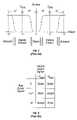
- FIG. 8illustrates a cross section of one embodiment of an array 100 comprising a transparent substrate 20 , a light direction layer 110 and a diffuser layer 120 .
- the array 100is an array of interferometric modulators.
- a light source 102such as an LED, is connected to the transparent substrate 20 such that light 104 (represented by reference numerals 104 a and 104 b ) emitted from the light source 102 enters the transparent substrate 20 and the light direction layer 110 .
- the light source 102is connected to a side surface 112 of the light direction layer 110 and the transparent substrate 20 .
- the light source 1 02may be connected to a side surface of just the light direction layer 110 .
- the structure of the light direction layer 110is optimized so that light 104 passing from the light source 102 into the transparent substrate 20 and the light direction layer 110 is redirected toward an array of elements 130 . Although a single ray 104 of light is depicted in FIG.
- the light source 102emits a beam of light having a given divergence and thus fills the entire transparent substrate 20 with light. Accordingly, a plurality of beams of light will be redirected toward the elements 130 . The majority of light from the light source 102 which does not contact the interface 114 between the diffuser layer 120 and the light direction layer 110 at a substantially perpendicular angle to the interface 114 to the diffuser layer 120 will not leak into the diff-user layer 120 , as discussed in further detail below. Preferably the light is directed in as narrow beams as possible.
- the term “light 104 ”represents beams of light and illustrates one of numerous light paths within those beams.
- the light source 102may be any suitable light source known in the art. Non-limiting examples include LEDs or fluorescent lights such as Cold Compact Fluorescent Lights.
- light 104 a emitted by light source 102is maintained within the light direction layer 110 and substrate 20 by total internal reflection until the light 104 a is redirected through the light direction layer 110 and substrate 20 into the elements 130 .
- the light direction layer 110may comprise a number of grooves 122 that provide surfaces off of which light 104 a may be reflected and redirected toward the elements 130 .
- the grooves 122contain air that is trapped in the space between the diffuser layer 120 and the light direction layer 110 .
- the grooves 122contain a low refractive index material.
- light 104 bmay be redirected toward the elements 130 in a narrow beam that is substantially perpendicular to the front surface of the substrate 20 .
- the majority of light 104 b that is transmitted through the light direction layer 110 and substrate 20 and directed into elements 130is reflected out of the elements 130 without being significantly affected by the grooves 122 .
- the reflecting structures 122 in the light direction layer 110are spaced such that light is directed to the elements 130 and not to the gap between the elements 132 , as shown in FIG. 8 .
- the elements 130are interferometric modulators.
- the systemis adapted for use as a backlight in a transmissive or transflective display.
- the elementsare other optical devices capable of reflecting light of a desired wavelength.
- the light direction layer 110can redirect light from the light source 102 into the elements 130 at the desired angle.
- strips or lines of reflective materialmay be incorporated within or placed on the light direction layer 110 at a diagonal angle.
- Lightmay be reflected off of a strip of the reflective material at an angle related to the material's diagonal angle and towards the elements 130 , in a manner similar to the manner described above with reference to the grooves 122 .
- the light 104 cis reflected out of the interferometric modulator elements 130 at an angle substantially perpendicular to the front surface substrate 20 . Consequently, and as will be discussed in further detail below, most light from the light source 102 does not directly leak into the diffuser layer 120 . However, light 104 c tended to be viewed as reflected from the interferometric modulator elements 130 is viewable because it interfaces with the diffuser layer 120 at a substantially perpendicular angle.
- the diffuser layer 120acts as a cover layer over the light direction layer 110 .
- the diffuser layer 120has a lower index of refraction than the light direction layer 110 and the transparent substrate 20 so that total internal reflection occurs at the interface 114 between the diffuser layer 120 and the light direction layer 110 .
- most light 104 a from the light source 102does not penetrate into the diffuser layer 120 . Consequently, the diffuser layer 120 is coupled with the light direction layer 110 without interacting with the light 104 a propagating in the light direction layer 110 and substrate 20 .
- the difference in the refractive index between the diffuser layer 120 and the light direction layer 110 and transparent substrate 20is directly proportional to the range of incidence angles over which the light 104 undergoes total internal reflection.
- the refractive index range of the diffuser layer 120is between 1.4 and 1.7.
- Suitable material candidates for the diffuser layer 120 which fall within this rangeinclude transparent or translucent polymer resin, for example, silicones, polyester, polycarbonate, polyvinyl chloride (PVC), polyvinylidene chloride, polystyrene, polyacrylates, polyethylene terephthalate, polyurethane, Zylar, and copolymers or blends thereof. In other embodiments other materials are used.
- the diffuser layer 120is a composite comprising a polymer resin as described above and one or more other components.
- the other componentis inorganic. In other embodiments, the other component is organic.
- the other componentmay be optical beads dispersed within the diffuser layer 120 .
- the diffuser layer 120comprises a film coated with micron-sized optical beads.
- the diffuser layer 120is a diffractive diff-user comprising diffractive surface relief on a thin plastic film.
- the diffuser layer 120is a pressure sensitive adhesive comprising suspended diffusing particles.
- the diffuser layer 120made from an inorganic material.
- the inorganic materialcomprises an oxide and/or nitride, for example, silica or alumina.
- the inorganic materialis crystalline.
- the inorganic materialis amorphous. In other embodiments other materials are used.
- the diffuser layer 120is monolithic.
- the material from which the diffuser layer 120 is manufacturedmay be inherently diffusive.
- a surface of the diff-user layer 120is patterned to provide diffusion. Either the surface of the diffuser layer 120 proximal to the viewer, the surface distal to the viewer, or both are patterned.
- the diffusive patternsmay comprise a random surface profile.
- the refractive index of the portion of the diffuser layer 120 proximal to the viewerhas a lower index of refraction than the light direction layer 110 and transparent substrate 20 , while the refractive index of the remaining portion of the diffuser layer 120 is unimportant.
- the diffuser layer 120is applied to the light direction layer 110 using an adhesive.
- the adhesiveis pre-applied to the diffuser layer 120 .
- the adhesiveis applied to the light direction layer 110 .
- Some embodimentsuse a two-part adhesive in which a first component is applied to the diffuser layer 120 and a second component is applied to the light direction layer 110 .
- the adhesiveis pressure sensitive.
- the adhesiveis thermosetting.
- the adhesivecures at about ambient temperature. In other embodiments, the adhesive is radiation-cured.
- the diffuser layer 120is fabricated on the light direction layer 110 .
- an uncured polymer resinis applied to the light direction layer 110 by means known in the art, for example, by spin coating, or calendaring. The polymer resin is then cured to form the diffuser layer 120 .
- the diffuser layer 120is comprised of a plastic film with a diffuser pressure sensitive adhesive, as discussed above.
- the diffuser layer 120is 200 ⁇ m thick. In other embodiments, the diffuser layer 120 is at least about 0.05 mm, at least about 0.1 mm, at least about 0.2 mm, or at least about 0.3 mm. In other embodiments the diffuser 120 is at least about 0.4 mm or at least about 0.5 mm. In some embodiments other thicknesses are also used.
- the refractive index of the light direction layer 110 and the transparent substrate 20is substantially equal. In certain embodiments, refractive indices are considered substantially equal if their values are within 2% of one another. For example, a substrate 20 with a refractive index of 1.52 may be coupled with a light direction layer 110 with a refractive index range between 1.49 and 1.54. As discussed herein, the refractive index of the light direction layer 110 will substantially equal the refractive index of the substrate 20 unless stated otherwise, although in other embodiments the refractive index of the light direction layer 110 may be less than the refractive index of the substrate 20 .
- the refractive index range of the light direction layer 110is between 1.40 and 1.65. Suitable material candidates for the light direction layer 110 which fall within this range include Zylar, polymethyl methacrylate, or polycarbonate. In some embodiments the light direction layer 110 is between 175 and 254 microns thick. In some embodiments other thicknesses are also used.
- the light direction layer 110contains grooves 122 that may be constructed by injection molding, controlled etching, or by any other process known to those of skill in the art.
- the light direction layer 110is a thin film containing surface relief.
- the light direction layer 110is thus also commonly referred to as a surface relief layer. Surface relief may be achieved using thin film embossing technology.
- the substrate 20 and the light direction layer 110are distinct objects, although in certain other embodiments, they are a single object such that the substrate 20 may include a light direction layer 110 .
- the light direction layer 110may be placed against the substrate 20 as depicted in FIG. 8 , or in a position such that there is a space between the light direction layer 110 and the substrate 20 .
- the substrate 20may comprise a transparent material such as, for example, glass, plastic, silica, alumina, and the like.
- the substrate 20is less than about 0.5 mm thick, for example, up to about 0.45 mm thick, or about 0.4 mm thick, or about 0.35 mm thick.
- the substrate 20is 700 microns thick.
- the substrate 20is no more than about 0.3 mm thick, about 0.25 mm thick, or about 0.2 mm thick.
- the substrate 20has a thickness of not great than about 0.15 mm thick or about 0.1 mm. In some embodiments other thicknesses are also used.
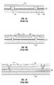
- FIG. 9illustrates a cross section of another embodiment of an array 200 comprising a transparent substrate 20 , a light direction layer 110 , a diffuser layer 120 and a high reflectance thin film 140 .
- the array 200is an array of interferometric modulators.
- a high reflectance thin film 140is located between the diffuser layer 120 and the light direction layer 110 .
- the high reflectance thin film 140has a lower index of refraction than the light direction layer 110 and the transparent substrate 20 so that total internal reflection occurs at the interface 116 between the high reflectance thin film 140 and the light direction layer 110 .
- the difference in the refractive index between the high reflectance thin film 140 and the light direction layer 110 and transparent substrate 20is directly proportional to the range of incidence angles over which the light 104 undergoes total internal reflection.
- the refractive index range of the high reflectance thin film 140is between 1.45 and 1.7.
- Suitable material candidates for the high reflectance thin film 140 which fall within this rangeinclude silicon dioxide, silicon nitride, di-aluminium tri-oxide, indium tin oxide, and molybdenum chromium.
- a stack of high reflectance thin film materialsare used. Suitable material candidates for high reflectance thin films to contain in a stack whose refractive index falls within this range include silicon nitride and silicon oxide.
- the films used in the stackalternate between high and low refractive index materials.
- the high reflectance thin film 140is between 200 and 300 nanometers thick. In some embodiments other thicknesses are also used.
- the high reflectance thin film 140is applied to the light direction layer 110 directly, while in other embodiments the high reflectance thin film 140 is deposited, such as by resistive evaporation or sputtering, onto a plastic film that is in turn applied to the light direction layer 110 .
- the diffuser layer 120is in contact with the high reflectance thin film 140 , as shown in FIG. 9 . In other embodiments, the diffuser layer 120 may be separated from the high reflectance thin film, such as by a different glass substrate.
- the diff-user layer 120may be physically coupled to either a high reflectance film 140 , as shown in FIG. 9 , or to a light direction layer 110 , as shown in FIG. 8 .
- the adjacent layermay nevertheless be optically distinct from the diffuser layer 120 , in that at least certain light incident at particular angles may not travel from the adjacent layer into the diffuser layer 120 .
- the adjacent layerhas a higher refractive index than the diffuser layer 120
- light incident at a shallow angle upon the boundary between the adjacent layer and the diffuser layer 120 at a shallow anglemay undergo total internal reflection and propagate within the adjacent layer, rather than entering the diffuser layer 120 .
- description of such layer as optically distinctdoes not preclude light from entering the diffuser layer 120 , as light incident upon the boundary at a sufficiently steep angle will not undergo total internal reflection, and will enter the diffuser layer 120 , as described above.
- the features, dimensions and materials of the array 200are the same as or similar to the features, dimensions and materials of the array 100 discussed above with reference to FIG. 8 , excluding the refractive index of the diffuser layer 120 .
- an interferometric modulator devicemay advantageously use a diffuser layer to obfuscate optical defects from the viewer's perception, enhancing an image without reducing the optical performance of the device, such as by both reducing contrast for ambient light and scattering ambient light within the light direction layer, the latter of which reduces front light brightness and creates non-uniformity issues.
Landscapes
- Physics & Mathematics (AREA)
- Spectroscopy & Molecular Physics (AREA)
- General Physics & Mathematics (AREA)
- Optics & Photonics (AREA)
- Mechanical Light Control Or Optical Switches (AREA)
Abstract
Description
Claims (41)
Priority Applications (1)
| Application Number | Priority Date | Filing Date | Title |
|---|---|---|---|
| US11/669,074US7777954B2 (en) | 2007-01-30 | 2007-01-30 | Systems and methods of providing a light guiding layer |
Applications Claiming Priority (1)
| Application Number | Priority Date | Filing Date | Title |
|---|---|---|---|
| US11/669,074US7777954B2 (en) | 2007-01-30 | 2007-01-30 | Systems and methods of providing a light guiding layer |
Publications (2)
| Publication Number | Publication Date |
|---|---|
| US20080180956A1 US20080180956A1 (en) | 2008-07-31 |
| US7777954B2true US7777954B2 (en) | 2010-08-17 |
Family
ID=39667755
Family Applications (1)
| Application Number | Title | Priority Date | Filing Date |
|---|---|---|---|
| US11/669,074Expired - Fee RelatedUS7777954B2 (en) | 2007-01-30 | 2007-01-30 | Systems and methods of providing a light guiding layer |
Country Status (1)
| Country | Link |
|---|---|
| US (1) | US7777954B2 (en) |
Cited By (28)
| Publication number | Priority date | Publication date | Assignee | Title |
|---|---|---|---|---|
| US20100141557A1 (en)* | 2006-10-06 | 2010-06-10 | Qualcomm Mems Technologies, Inc. | Light guide |
| US20100165443A1 (en)* | 2004-09-27 | 2010-07-01 | Qualcomm Mems Technologies, Inc. | Systems and methods using interferometric optical modulators and diffusers |
| US7864395B2 (en) | 2006-10-27 | 2011-01-04 | Qualcomm Mems Technologies, Inc. | Light guide including optical scattering elements and a method of manufacture |
| US20110030773A1 (en)* | 2009-08-06 | 2011-02-10 | Alliance For Sustainable Energy, Llc | Photovoltaic cell with back-surface reflectivity scattering |
| US7907319B2 (en) | 1995-11-06 | 2011-03-15 | Qualcomm Mems Technologies, Inc. | Method and device for modulating light with optical compensation |
| US7933475B2 (en) | 2006-02-17 | 2011-04-26 | Qualcomm Mems Technologies, Inc. | Method and apparatus for providing back-lighting in a display device |
| US8040589B2 (en) | 2008-02-12 | 2011-10-18 | Qualcomm Mems Technologies, Inc. | Devices and methods for enhancing brightness of displays using angle conversion layers |
| US8045252B2 (en) | 2004-02-03 | 2011-10-25 | Qualcomm Mems Technologies, Inc. | Spatial light modulator with integrated optical compensation structure |
| US8045256B2 (en) | 2004-09-27 | 2011-10-25 | Qualcomm Mems Technologies, Inc. | Method and device for compensating for color shift as a function of angle of view |
| US8049951B2 (en) | 2008-04-15 | 2011-11-01 | Qualcomm Mems Technologies, Inc. | Light with bi-directional propagation |
| US8061882B2 (en) | 2006-10-06 | 2011-11-22 | Qualcomm Mems Technologies, Inc. | Illumination device with built-in light coupler |
| US8068710B2 (en) | 2007-12-07 | 2011-11-29 | Qualcomm Mems Technologies, Inc. | Decoupled holographic film and diffuser |
| US8107155B2 (en) | 2006-10-06 | 2012-01-31 | Qualcomm Mems Technologies, Inc. | System and method for reducing visual artifacts in displays |
| US8111446B2 (en) | 2004-09-27 | 2012-02-07 | Qualcomm Mems Technologies, Inc. | Optical films for controlling angular characteristics of displays |
| US8300304B2 (en) | 2008-02-12 | 2012-10-30 | Qualcomm Mems Technologies, Inc. | Integrated front light diffuser for reflective displays |
| US8346048B2 (en) | 2008-05-28 | 2013-01-01 | Qualcomm Mems Technologies, Inc. | Front light devices and methods of fabrication thereof |
| US8368981B2 (en) | 2006-10-10 | 2013-02-05 | Qualcomm Mems Technologies, Inc. | Display device with diffractive optics |
| US8466447B2 (en) | 2009-08-06 | 2013-06-18 | Alliance For Sustainable Energy, Llc | Back contact to film silicon on metal for photovoltaic cells |
| US8596846B2 (en) | 2012-03-16 | 2013-12-03 | Nano-Optic Devices, Llc | Frontlight unit for enhancing illumination of a reflective display |
| US8902484B2 (en) | 2010-12-15 | 2014-12-02 | Qualcomm Mems Technologies, Inc. | Holographic brightness enhancement film |
| US8928967B2 (en) | 1998-04-08 | 2015-01-06 | Qualcomm Mems Technologies, Inc. | Method and device for modulating light |
| US8971675B2 (en) | 2006-01-13 | 2015-03-03 | Qualcomm Mems Technologies, Inc. | Interconnect structure for MEMS device |
| US8979349B2 (en) | 2009-05-29 | 2015-03-17 | Qualcomm Mems Technologies, Inc. | Illumination devices and methods of fabrication thereof |
| US9019183B2 (en) | 2006-10-06 | 2015-04-28 | Qualcomm Mems Technologies, Inc. | Optical loss structure integrated in an illumination apparatus |
| US9025235B2 (en) | 2002-12-25 | 2015-05-05 | Qualcomm Mems Technologies, Inc. | Optical interference type of color display having optical diffusion layer between substrate and electrode |
| US9110289B2 (en) | 1998-04-08 | 2015-08-18 | Qualcomm Mems Technologies, Inc. | Device for modulating light with multiple electrodes |
| US9164219B2 (en) | 2011-11-14 | 2015-10-20 | Nano-Optic Devices, Llc | Frontlight unit for reflective displays |
| US20170102497A1 (en)* | 2015-10-13 | 2017-04-13 | E Ink Holdings Inc. | Reflective display apparatus and front light module thereof |
Families Citing this family (8)
| Publication number | Priority date | Publication date | Assignee | Title |
|---|---|---|---|---|
| US7750886B2 (en)* | 2004-09-27 | 2010-07-06 | Qualcomm Mems Technologies, Inc. | Methods and devices for lighting displays |
| US7766498B2 (en) | 2006-06-21 | 2010-08-03 | Qualcomm Mems Technologies, Inc. | Linear solid state illuminator |
| US7845841B2 (en) | 2006-08-28 | 2010-12-07 | Qualcomm Mems Technologies, Inc. | Angle sweeping holographic illuminator |
| US7855827B2 (en) | 2006-10-06 | 2010-12-21 | Qualcomm Mems Technologies, Inc. | Internal optical isolation structure for integrated front or back lighting |
| US7733439B2 (en) | 2007-04-30 | 2010-06-08 | Qualcomm Mems Technologies, Inc. | Dual film light guide for illuminating displays |
| US8552965B2 (en)* | 2007-10-30 | 2013-10-08 | Nlt Technologies, Ltd. | Display device and electronic appliance |
| TWI485452B (en)* | 2012-10-31 | 2015-05-21 | Compal Electronics Inc | Composite light guide plate manufacturing method |
| JP6457872B2 (en) | 2015-04-10 | 2019-01-23 | 株式会社ジャパンディスプレイ | Display device, lighting device, light guide plate, and manufacturing method thereof |
Citations (360)
| Publication number | Priority date | Publication date | Assignee | Title |
|---|---|---|---|---|
| US2518647A (en) | 1948-01-07 | 1950-08-15 | Celanese Corp | Interferometer means for thickness measurements |
| US3813265A (en) | 1970-02-16 | 1974-05-28 | A Marks | Electro-optical dipolar material |
| US3924929A (en) | 1966-11-14 | 1975-12-09 | Minnesota Mining & Mfg | Retro-reflective sheet material |
| US4375312A (en) | 1980-08-07 | 1983-03-01 | Hughes Aircraft Company | Graded index waveguide structure and process for forming same |
| US4378567A (en) | 1981-01-29 | 1983-03-29 | Eastman Kodak Company | Electronic imaging apparatus having means for reducing inter-pixel transmission nonuniformity |
| DE3402746A1 (en) | 1984-01-27 | 1985-08-08 | Robert Bosch Gmbh, 7000 Stuttgart | Liquid crystal display |
| EP0278038A1 (en) | 1987-02-13 | 1988-08-17 | Battelle-Institut e.V. | Active flat type display panel |
| US4832459A (en) | 1984-02-06 | 1989-05-23 | Rogers Corporation | Backlighting for electro-optical passive displays and transflective layer useful therewith |
| US4850682A (en) | 1986-07-14 | 1989-07-25 | Advanced Environmental Research Group | Diffraction grating structures |
| US4961617A (en) | 1989-07-19 | 1990-10-09 | Ferrydon Shahidi | Fibre optic waveguide illuminating elements |
| US5050946A (en) | 1990-09-27 | 1991-09-24 | Compaq Computer Corporation | Faceted light pipe |
| US5226099A (en) | 1991-04-26 | 1993-07-06 | Texas Instruments Incorporated | Digital micromirror shutter device |
| US5289300A (en) | 1991-02-04 | 1994-02-22 | Semiconductor Energy Laboratory Co., Ltd. | Method of manufacturing electro-optical devices wherein the electrode is patterned on the modulation layer |
| EP0590511A1 (en) | 1992-10-01 | 1994-04-06 | International Business Machines Corporation | Edge-lit transflective non-emissive display |
| GB2260203B (en) | 1991-10-04 | 1994-09-07 | Marconi Gec Ltd | Colour display system |
| GB2278222A (en) | 1993-05-20 | 1994-11-23 | Sharp Kk | Spatial light modulator |
| US5398125A (en) | 1993-11-10 | 1995-03-14 | Minnesota Mining And Manufacturing Company | Liquid crystal projection panel having microlens arrays, on each side of the liquid crystal, with a focus beyond the liquid crystal |
| US5452385A (en) | 1993-03-09 | 1995-09-19 | Sharp Kabushiki Kaisha | Optical scanning device an optical scanning type display and an image data input/output device |
| US5467417A (en) | 1992-09-16 | 1995-11-14 | Hitachi, Ltd. | Prism plate for efficiently emitting light flux within a predetermined range, and liquid crystal indicator and indicator illumination method using the same |
| US5481385A (en) | 1993-07-01 | 1996-01-02 | Alliedsignal Inc. | Direct view display device with array of tapered waveguide on viewer side |
| US5515184A (en) | 1991-11-12 | 1996-05-07 | The University Of Alabama In Huntsville | Waveguide hologram illuminators |
| US5555160A (en) | 1991-06-27 | 1996-09-10 | Nissen Chemitec Co., Ltd. | Light-guiding panel for surface lighting and a surface lighting body |
| US5592332A (en) | 1992-12-25 | 1997-01-07 | Dai Nippon Printing Co., Ltd. | Renticular lens, surface light source, and liquid crystal display apparatus |
| US5594830A (en) | 1992-03-23 | 1997-01-14 | Minnesota Mining And Manufacturing Co. | Luminaire device |
| US5638084A (en) | 1992-05-22 | 1997-06-10 | Dielectric Systems International, Inc. | Lighting-independent color video display |
| US5647036A (en) | 1994-09-09 | 1997-07-08 | Deacon Research | Projection display with electrically-controlled waveguide routing |
| US5650865A (en) | 1995-03-21 | 1997-07-22 | Hughes Electronics | Holographic backlight for flat panel displays |
| US5659410A (en) | 1993-12-28 | 1997-08-19 | Enplas Corporation | Surface light source device and liquid crystal display |
| US5671314A (en) | 1993-01-15 | 1997-09-23 | Sisters Of Prividence In Oregon | Illuminator devices for ultraviolet light delivery and methods of making same |
| US5673128A (en) | 1995-01-31 | 1997-09-30 | Sharp Kabushiki Kaisha | Back light device of liquid crystal device |
| US5671994A (en) | 1994-06-08 | 1997-09-30 | Clio Technologies, Inc. | Flat and transparent front-lighting system using microprisms |
| DE19622748A1 (en) | 1996-06-05 | 1997-12-11 | Forschungszentrum Juelich Gmbh | Interference filter based on porous silicon |
| US5703667A (en) | 1996-05-31 | 1997-12-30 | Shimada Precision, Co., Ltd. | Light guide plates and light guide plate assembly utilizing diffraction grating |
| US5735590A (en) | 1994-03-02 | 1998-04-07 | Tosoh Corporation | Backlighting device with a transparent sheet having straight ridges |
| US5771321A (en) | 1996-01-04 | 1998-06-23 | Massachusetts Institute Of Technology | Micromechanical optical switch and flat panel display |
| US5783614A (en) | 1997-02-21 | 1998-07-21 | Copytele, Inc. | Polymeric-coated dielectric particles and formulation and method for preparing same |
| GB2321532A (en) | 1997-01-22 | 1998-07-29 | Sharp Kk | Multi-colour reflector device and display |
| US5805117A (en) | 1994-05-12 | 1998-09-08 | Samsung Electronics Co., Ltd. | Large area tiled modular display system |
| US5810464A (en) | 1995-02-03 | 1998-09-22 | Enplas Corporation | Surface light source device of side light type |
| US5815229A (en) | 1994-11-21 | 1998-09-29 | Proxima Corporation | Microlens imbedded liquid crystal projection panel including thermal insulation layer |
| US5854872A (en) | 1996-10-08 | 1998-12-29 | Clio Technologies, Inc. | Divergent angle rotator system and method for collimating light beams |
| EP0822441A3 (en) | 1996-08-01 | 1998-12-30 | Sharp Kabushiki Kaisha | Optical device and directional display |
| US5883684A (en) | 1997-06-19 | 1999-03-16 | Three-Five Systems, Inc. | Diffusively reflecting shield optically, coupled to backlit lightguide, containing LED's completely surrounded by the shield |
| US5892598A (en) | 1994-07-15 | 1999-04-06 | Matsushita Electric Industrial Co., Ltd. | Head up display unit, liquid crystal display panel, and method of fabricating the liquid crystal display panel |
| EP0907050A1 (en) | 1997-10-03 | 1999-04-07 | THOMSON multimedia | Back-lighting system for a transmissive electrooptic modulator using the light polarization effect |
| EP0879991A3 (en) | 1997-05-13 | 1999-04-21 | Matsushita Electric Industrial Co., Ltd. | Illuminating system |
| GB2331615A (en) | 1997-11-21 | 1999-05-26 | Mitsubishi Electric Corp | A backlight for a liquid crystal display |
| US5914804A (en) | 1998-01-28 | 1999-06-22 | Lucent Technologies Inc | Double-cavity micromechanical optical modulator with plural multilayer mirrors |
| US5913594A (en) | 1997-02-25 | 1999-06-22 | Iimura; Keiji | Flat panel light source device and passive display device utilizing the light source device |
| US5933183A (en) | 1995-12-12 | 1999-08-03 | Fuji Photo Film Co., Ltd. | Color spatial light modulator and color printer using the same |
| US5956106A (en) | 1993-07-27 | 1999-09-21 | Physical Optics Corporation | Illuminated display with light source destructuring and shaping device |
| US5982540A (en) | 1994-03-16 | 1999-11-09 | Enplas Corporation | Surface light source device with polarization function |
| EP0957392A1 (en) | 1998-05-11 | 1999-11-17 | Nitto Denko Corporation | Reflection type liquid-crystal display unit |
| US5991073A (en) | 1996-01-26 | 1999-11-23 | Sharp Kabushiki Kaisha | Autostereoscopic display including a viewing window that may receive black view data |
| US5999239A (en) | 1995-04-07 | 1999-12-07 | Honeywell Inc. | Method for making a polarization-sensitive optical element |
| US6002829A (en) | 1992-03-23 | 1999-12-14 | Minnesota Mining And Manufacturing Company | Luminaire device |
| US6014192A (en) | 1996-07-16 | 2000-01-11 | Thomson-Csf | Illumination device and application thereof to the illumination of a transmissive screen |
| GB2340281A (en) | 1998-08-04 | 2000-02-16 | Sharp Kk | A reflective liquid crystal display device |
| JP2000075293A (en) | 1998-09-02 | 2000-03-14 | Matsushita Electric Ind Co Ltd | Illumination device, illuminated touch panel and reflective liquid crystal display device |
| JP2000081848A (en) | 1998-09-03 | 2000-03-21 | Semiconductor Energy Lab Co Ltd | Electronic equipment mounting liquid crystal display device |
| US6040937A (en) | 1994-05-05 | 2000-03-21 | Etalon, Inc. | Interferometric modulation |
| US6048071A (en) | 1997-03-28 | 2000-04-11 | Sharp Kabushiki Kaisha | Front illumination device and reflection-type liquid crystal display device incorporating same |
| US6049317A (en) | 1989-02-27 | 2000-04-11 | Texas Instruments Incorporated | System for imaging of light-sensitive media |
| US6073034A (en) | 1996-10-31 | 2000-06-06 | Kopin Corporation | Wireless telephone display system |
| US6074069A (en) | 1998-11-17 | 2000-06-13 | Industrial Technology Research Institute | Backlight source device with circular arc diffusion units |
| JP2000193933A (en) | 1998-12-25 | 2000-07-14 | Matsushita Electric Works Ltd | Display device |
| US6091469A (en)* | 1998-05-19 | 2000-07-18 | Dai Nippon Printing Co., Ltd. | Light reflector for use in a reflective-type liquid-crystal display |
| US6099134A (en) | 1996-09-27 | 2000-08-08 | Hitachi, Ltd. | Liquid crystal display device |
| US6128077A (en) | 1997-11-17 | 2000-10-03 | Max Planck Gesellschaft | Confocal spectroscopy system and method |
| JP2000305074A (en) | 1999-04-26 | 2000-11-02 | Dainippon Printing Co Ltd | Reflective liquid crystal display |
| CN1272922A (en) | 1998-06-02 | 2000-11-08 | 日本写真印刷株式会社 | Touch screen device with front lighting |
| US6151089A (en) | 1998-01-20 | 2000-11-21 | Sony Corporation | Reflection type display with light waveguide with inclined and planar surface sections |
| JP2001021883A (en) | 1999-07-06 | 2001-01-26 | Nec Corp | Reflective liquid crystal display device and electronic equipment |
| US6195196B1 (en) | 1998-03-13 | 2001-02-27 | Fuji Photo Film Co., Ltd. | Array-type exposing device and flat type display incorporating light modulator and driving method thereof |
| US6196691B1 (en) | 1998-04-01 | 2001-03-06 | Shimada Precision, Co., Ltd. | Light guide plate for point source |
| CN1286424A (en) | 1999-08-31 | 2001-03-07 | 大赛璐化学工业株式会社 | Touch screen and display device using said touch screen |
| DE19942513A1 (en) | 1999-09-07 | 2001-03-08 | Gerhard Karl | Luminous body for images capable of screening |
| US6199989B1 (en) | 1998-10-29 | 2001-03-13 | Sumitomo Chemical Company, Limited | Optical plate having reflecting function and transmitting function |
| US6211976B1 (en) | 1998-09-14 | 2001-04-03 | Digilens, Inc. | Holographic projection system |
| US20010010630A1 (en) | 2000-01-13 | 2001-08-02 | Seiji Umemoto | Light pipe and method for producing the same |
| US6273577B1 (en) | 1997-10-31 | 2001-08-14 | Sanyo Electric Co., Ltd. | Light guide plate, surface light source using the light guide plate, and liquid crystal display using the surface light source |
| US6282010B1 (en) | 1998-05-14 | 2001-08-28 | Texas Instruments Incorporated | Anti-reflective coatings for spatial light modulators |
| US20010019380A1 (en) | 2000-03-03 | 2001-09-06 | Takayuki Ishihara | Lighting unit and liquid crystal display utilizing the same |
| US20010022636A1 (en) | 1997-03-25 | 2001-09-20 | Sony Corporation | Reflective display device |
| US20010030861A1 (en) | 1996-02-01 | 2001-10-18 | Mitsubishi Rayon Co., Ltd. | Surface light source device, and liquid crystal display device, sign display apparatus and traffic sign display apparatus using the surface light source device |
| JP2001305312A (en) | 2000-03-31 | 2001-10-31 | Three M Innovative Properties Co | Optical laminated body |
| US20010049061A1 (en) | 1997-12-05 | 2001-12-06 | Shintaro Nakagaki | Method for producing hologram lens, method for producing hologram color filter, and space light modulating apparatuses using the hologram lens and the hologram color filter respectively |
| JP2001343514A (en) | 2000-05-30 | 2001-12-14 | Victor Co Of Japan Ltd | Hologram color filter |
| US20010055208A1 (en) | 2000-06-15 | 2001-12-27 | Koichi Kimura | Optical element, optical light source unit and optical display device equipped with the optical light source unit |
| US20020006036A1 (en) | 2000-07-11 | 2002-01-17 | Minebea Co., Ltd. | Spread illuminating apparatus |
| US20020024711A1 (en) | 1994-05-05 | 2002-02-28 | Iridigm Display Corporation, A Delaware Corporation | Interferometric modulation of radiation |
| US6356378B1 (en) | 1995-06-19 | 2002-03-12 | Reflectivity, Inc. | Double substrate reflective spatial light modulator |
| US20020034071A1 (en) | 2000-09-20 | 2002-03-21 | Sanyo Electric Co., Ltd. | Beam light source and lighting device using same |
| JP2002090549A (en) | 2000-09-13 | 2002-03-27 | Shimada Precision Kk | Front light light guide plate |
| JP2002108227A (en) | 2000-07-26 | 2002-04-10 | Bridgestone Corp | Front light and liquid crystal display device |
| US6371623B1 (en) | 1999-08-16 | 2002-04-16 | Minebea Co., Ltd. | Spread illuminating apparatus with a means for controlling light directivity |
| US20020044445A1 (en) | 1999-12-03 | 2002-04-18 | Bohler Christopher L. | Sold state light source augmentation for slm display systems |
| EP1199512A1 (en) | 2000-10-11 | 2002-04-24 | Nitto Denko Corporation | Glass substrate and liquid-crystal display device |
| US6381022B1 (en) | 1992-01-22 | 2002-04-30 | Northeastern University | Light modulating device |
| US20020051354A1 (en) | 2000-11-02 | 2002-05-02 | Minebea Co., Ltd. | Spread illuminating apparatus with a pair of light sources overlapped in a thickness direction of a transparent substrate |
| US20020054258A1 (en) | 2000-11-08 | 2002-05-09 | Nitto Denko Corporation | Optical film and reflective liquid-crystal display device |
| US20020054424A1 (en) | 1994-05-05 | 2002-05-09 | Etalon, Inc. | Photonic mems and structures |
| US6407785B1 (en) | 1998-10-05 | 2002-06-18 | Semiconductor Energy Laboratory Co., Ltd. | Reflection type semiconductor display device having optical fiber adjacent the surface of the main body |
| JP2002174780A (en) | 2000-12-08 | 2002-06-21 | Stanley Electric Co Ltd | Reflective color display |
| US20020080465A1 (en) | 2000-11-03 | 2002-06-27 | Intpax, Inc. | MEMS based variable optical attenuator (MBVOA) |
| US6412969B1 (en) | 1998-12-14 | 2002-07-02 | Sharp Kabushiki Kaisha | Backlighting device and a method of manufacturing the same, and a liquid crystal display apparatus |
| JP2002196151A (en) | 2000-12-25 | 2002-07-10 | Citizen Electronics Co Ltd | Light guide plate |
| US20020106182A1 (en) | 2001-02-02 | 2002-08-08 | Minebea Co., Ltd. | Spread illuminating apparatus with cover provided over transparent substrate |
| US20020105699A1 (en) | 2001-02-02 | 2002-08-08 | Teravicta Technologies, Inc | Integrated optical micro-electromechanical systems and methods of fabricating and operating the same |
| JP2002245835A (en) | 2001-02-15 | 2002-08-30 | Minolta Co Ltd | Illumination device, display device, and electronic equipment |
| US6456279B1 (en) | 1998-07-14 | 2002-09-24 | Hitachi, Ltd. | Liquid crystal display device with a touch panel |
| US6454452B1 (en) | 1999-04-22 | 2002-09-24 | Mitsubishi Denki Kabushiki Kaisha | Backlight for liquid crystal display device |
| US20020135560A1 (en) | 2001-03-26 | 2002-09-26 | Minebea Co., Ltd. | Spread illuminating apparatus with multi-layer light conductive member |
| US20020149584A1 (en) | 2001-04-13 | 2002-10-17 | Simpson John T. | Reflective coherent spatial light modulator |
| US20020154256A1 (en) | 2001-02-09 | 2002-10-24 | Fujitsu Limited | Liquid-crystal display and a lighting apparatus |
| US6478432B1 (en) | 2001-07-13 | 2002-11-12 | Chad D. Dyner | Dynamically generated interactive real imaging device |
| US20020172039A1 (en) | 2001-05-16 | 2002-11-21 | Ben-Zion Inditsky | Ultra-thin backlight |
| CN1381752A (en) | 2001-04-16 | 2002-11-27 | 日东电工株式会社 | Contact screen with lighting device and reflection liquid crystal display unit |
| US20020180910A1 (en) | 2001-05-07 | 2002-12-05 | Nitto Denko Corporation | Reflective liquid-crystal display device |
| US6493475B1 (en) | 2000-10-19 | 2002-12-10 | Tellium, Inc. | Monolithic integration of signal-monitoring scheme in an optical switch |
| EP1271223A2 (en) | 2001-06-28 | 2003-01-02 | Nokia Corporation | Electronic display |
| US6504589B1 (en) | 1997-02-18 | 2003-01-07 | Dai Nippon Printing Co., Ltd. | Backlight device and liquid crystal display device |
| JP2003007114A (en) | 2001-06-26 | 2003-01-10 | Sharp Corp | Front light and reflective display device using the same |
| US20030012009A1 (en) | 2001-07-13 | 2003-01-16 | Minebea Co., Ltd | Spread illuminating apparatus with light reflection member |
| US20030016930A1 (en) | 2001-07-23 | 2003-01-23 | Ben-Zion Inditsky | Ultra thin radiation management and distribution systems with hybrid optical waveguide |
| US6512626B1 (en) | 1999-06-16 | 2003-01-28 | Creavis Gesellschaft Fuer Technologie Und Innovation Mbh | Composite sheets with electrically switchable optical properties made of light-scattering base material |
| EP1279892A1 (en) | 2001-07-27 | 2003-01-29 | Nissen Chemitec Corporation | Planar lighting device |
| US20030030764A1 (en) | 2001-07-13 | 2003-02-13 | Hea-Chun Lee | Light guiding plate, method of manufacturing the same and liquid crystal display having the light guiding plate |
| US6522794B1 (en) | 1994-09-09 | 2003-02-18 | Gemfire Corporation | Display panel with electrically-controlled waveguide-routing |
| JP2003057652A (en) | 2001-08-20 | 2003-02-26 | Japan Science & Technology Corp | Image display devices, lighting devices |
| JP2003066451A (en) | 2001-08-30 | 2003-03-05 | Matsushita Electric Ind Co Ltd | Liquid crystal display |
| US20030043157A1 (en) | 1999-10-05 | 2003-03-06 | Iridigm Display Corporation | Photonic MEMS and structures |
| US6538813B1 (en) | 2000-09-19 | 2003-03-25 | Honeywell International Inc. | Display screen with metallized tapered waveguides |
| US20030067760A1 (en) | 2001-09-26 | 2003-04-10 | Jagt Hendrik Johannes Boudewijn | Waveguide, edge-lit illumination arrangement and display comprising such |
| US20030071947A1 (en) | 2001-07-05 | 2003-04-17 | Miki Shiraogawa | Optical film and a liquid crystal display using the same |
| US20030083429A1 (en) | 1995-09-28 | 2003-05-01 | Alliedsignal Inc. | Colored articles and compositions and methods for their fabrication |
| EP1306609A1 (en) | 2001-10-23 | 2003-05-02 | Alps Electric Co., Ltd. | Surface-emitting device and liquid crystal display device with enhanced utilization efficiency of light from light source |
| US20030086031A1 (en) | 2000-06-29 | 2003-05-08 | Hitoshi Taniguchi | Liquid crystal display device |
| US20030090887A1 (en) | 2001-11-12 | 2003-05-15 | Nidec Copal Corporation | Light-guide plate and method for manufacturing the same |
| US20030095401A1 (en) | 2001-11-20 | 2003-05-22 | Palm, Inc. | Non-visible light display illumination system and method |
| US20030098957A1 (en) | 2001-11-28 | 2003-05-29 | Haldiman Robert C. | System, method and apparatus for ambient video projection |
| US20030099118A1 (en) | 2001-11-29 | 2003-05-29 | Nec Corporation | Light source and liquid crystal display device using this light source |
| US6574033B1 (en) | 2002-02-27 | 2003-06-03 | Iridigm Display Corporation | Microelectromechanical systems device and method for fabricating same |
| US20030103344A1 (en) | 2001-11-30 | 2003-06-05 | Eiki Niida | Wedge plate type light guiding plate for front light |
| US20030103177A1 (en) | 2001-04-10 | 2003-06-05 | Seiko Epson Corporation | Liquid crystal device and electronic apparatus |
| US6577429B1 (en) | 2002-01-15 | 2003-06-10 | Eastman Kodak Company | Laser projection display system |
| JP2003173713A (en) | 2001-12-04 | 2003-06-20 | Rohm Co Ltd | Illumination device and liquid crystal display device |
| US6582095B1 (en) | 1999-07-23 | 2003-06-24 | Minebea Co., Ltd. | Spread illuminating apparatus |
| US20030123245A1 (en) | 1995-06-27 | 2003-07-03 | Parker Jeffery R. | Light emitting panel assemblies |
| JP2003188959A (en) | 2001-12-14 | 2003-07-04 | Nec Access Technica Ltd | Portable telephone set |
| US6592234B2 (en) | 2001-04-06 | 2003-07-15 | 3M Innovative Properties Company | Frontlit display |
| US6598987B1 (en) | 2000-06-15 | 2003-07-29 | Nokia Mobile Phones Limited | Method and apparatus for distributing light to the user interface of an electronic device |
| US6603520B2 (en) | 2000-12-21 | 2003-08-05 | Nitto Denko Corporation | Optical film and liquid-crystal display device |
| US20030151821A1 (en) | 2001-12-19 | 2003-08-14 | Favalora Gregg E. | Radiation conditioning system |
| EP1336876A1 (en) | 2002-02-05 | 2003-08-20 | Alps Electric Co., Ltd. | Illumination device having a single light source and liquid crystal display device |
| US20030161040A1 (en) | 2002-02-26 | 2003-08-28 | Namco Ltd. | Stereoscopic image display device and electronic apparatus |
| US20030160919A1 (en) | 2002-02-28 | 2003-08-28 | Mitsubishi Denki Kabushiki Kaisha | Liquid crystal display device |
| US20030169385A1 (en) | 2002-03-05 | 2003-09-11 | Citizen Electronics Co., Ltd. | Illumination device for a color liquid crystal display |
| EP1347315A1 (en) | 2000-12-28 | 2003-09-24 | Fuji Electric Co., Ltd. | Light guiding plate and liquid crystal display device with the light guiding plate |
| US20030184690A1 (en) | 2000-04-21 | 2003-10-02 | Akifumi Ogiwara | Illuminator, image display comprising the same, liquid crystal television, liquid crystal monitor, and liquid crystal information terminal |
| US6631998B2 (en) | 2000-09-05 | 2003-10-14 | Minebea Co., Ltd. | Spread illuminating apparatus |
| US20030193630A1 (en) | 2002-04-10 | 2003-10-16 | Au Optronics Corp. | Light guide plate capable of controlling light-emitting angle and liquid crystal display therewith |
| US6636358B2 (en) | 2000-02-02 | 2003-10-21 | Nitto Denko Corporation | Optical film |
| US6636322B1 (en) | 1999-05-07 | 2003-10-21 | Sharp Kabushiki Kaisha | Method and device for measuring cell gap of liquid crystal display using near-IR radiation |
| US6642913B1 (en) | 1999-01-20 | 2003-11-04 | Fuji Photo Film Co., Ltd. | Light modulation element, exposure unit, and flat-panel display unit |
| JP2003315694A (en) | 2002-04-25 | 2003-11-06 | Fuji Photo Film Co Ltd | Image display element and image display device using the same |
| US20030210222A1 (en) | 2000-07-31 | 2003-11-13 | Akifumi Ogiwara | Illuminator, image display, liquid crystal monitor, liquid crystal television, liquid crystal information terminal, and method for producing light guide plate |
| US20030210363A1 (en) | 2000-04-21 | 2003-11-13 | Seiko Epson Corporation | Electrooptical device, projection-type display apparatus, and method for manufacturing the electrooptical device |
| US20030210367A1 (en) | 2002-05-07 | 2003-11-13 | Nitto Denko Corporation | Reflection-type liquid-crystal display, and optical film |
| US20030214728A1 (en) | 2002-05-20 | 2003-11-20 | General Electric Company | Optical substrate and method of making |
| US6652109B2 (en) | 2000-12-14 | 2003-11-25 | Alps Electric Co., Ltd. | Surface light emission device, method of manufacturing the same, and liquid crystal display device |
| US6657683B2 (en) | 1999-10-22 | 2003-12-02 | Motorola, Inc. | Front illuminator for a liquid crystal display and method of making same |
| JP2003344881A (en) | 2002-05-22 | 2003-12-03 | Alps Electric Co Ltd | Electrophoretic display |
| US6660997B2 (en) | 2001-04-26 | 2003-12-09 | Creo Srl | Absolute position Moiré type encoder for use in a control system |
| US6669350B2 (en) | 2000-12-14 | 2003-12-30 | Mitsubish Rayon Co., Ltd. | Planar light source system and light deflecting device therefor |
| US20040001169A1 (en) | 2002-02-12 | 2004-01-01 | Yuuji Saiki | Polarizer, polarizing plate, liquid crystal display, and image display, and a method for producing the polarizer |
| US6674562B1 (en) | 1994-05-05 | 2004-01-06 | Iridigm Display Corporation | Interferometric modulation of radiation |
| US20040017599A1 (en) | 2002-07-29 | 2004-01-29 | Xiaofeng Yang | Micro-mirror with rotor structure |
| US20040027315A1 (en) | 2002-08-09 | 2004-02-12 | Sanyo Electric Co., Ltd. | Display including a plurality of display panels |
| US20040032401A1 (en) | 2002-08-19 | 2004-02-19 | Fujitsu Limited | Touch panel device |
| EP1329664A4 (en) | 2000-09-25 | 2004-03-03 | Mitsubishi Rayon Co | LIGHTING DEVICE |
| US20040042233A1 (en) | 2002-08-30 | 2004-03-04 | Fujitsu Display Technologies Corporation | Lighting unit and display device |
| US6709123B2 (en) | 2000-02-04 | 2004-03-23 | Robert Bosch Gmbh | Display device |
| US20040070711A1 (en) | 2002-10-11 | 2004-04-15 | Chi-Jain Wen | Double-sided LCD panel |
| EP1413543A1 (en) | 2002-10-24 | 2004-04-28 | Hewlett-Packard Development Company, L.P. | Micro electro mechanical (MEMS) actuated colour light modulator grating and method for its manufacture |
| US20040080938A1 (en) | 2001-12-14 | 2004-04-29 | Digital Optics International Corporation | Uniform illumination system |
| US20040085748A1 (en) | 2002-10-16 | 2004-05-06 | Alps Electric Co., Ltd. | Lighting device and liquid crystal display device |
| US6738194B1 (en) | 2002-07-22 | 2004-05-18 | The United States Of America As Represented By The Secretary Of The Navy | Resonance tunable optical filter |
| US20040100796A1 (en) | 2002-11-21 | 2004-05-27 | Matthew Ward | Light emitting diode (LED) picture element |
| US6742907B2 (en) | 1996-09-24 | 2004-06-01 | Seiko Epson Corporation | Illumination device and display device using it |
| US6742921B2 (en)* | 2000-06-26 | 2004-06-01 | Nitto Denko Corporation | Light pipe, plate light source unit and reflection type liquid-crystal display device |
| US20040109305A1 (en) | 2002-12-04 | 2004-06-10 | General Electric Company | High index coated light management films |
| US6751023B2 (en) | 2000-02-02 | 2004-06-15 | Nitto Denko Corporation | Optical film |
| US20040125281A1 (en) | 2002-12-25 | 2004-07-01 | Wen-Jian Lin | Optical interference type of color display |
| US20040125048A1 (en) | 2002-09-20 | 2004-07-01 | Toshihiro Fukuda | Display element , display device, and microlens array |
| US6760135B1 (en) | 1999-06-09 | 2004-07-06 | Holographic Imaging Llc | Holographic displays |
| US6761461B2 (en) | 2001-11-15 | 2004-07-13 | Minebea Co., Ltd. | Spread illuminating apparatus without light conductive bar |
| EP1437610A1 (en) | 2003-01-07 | 2004-07-14 | Samsung Electronics Co., Ltd. | Backlight unit |
| US6773126B1 (en) | 1999-05-28 | 2004-08-10 | Oy Modilis Ltd. | Light panel with improved diffraction |
| US6774962B2 (en) | 2001-11-08 | 2004-08-10 | Lg.Philips Lcd Co., Ltd. | Liquid crystal display device using cholesteric liquid crystal and a manufacturing method thereof |
| EP1445629A1 (en) | 2003-02-04 | 2004-08-11 | Fawoo Technology Co., Ltd | A light guide panel with slant light guiding parts |
| US6778746B2 (en) | 1997-05-16 | 2004-08-17 | Btg International Limited | Optical devices and methods of fabrication thereof |
| DE10228946B4 (en) | 2002-06-28 | 2004-08-26 | Universität Bremen | Optical modulator, display, use of an optical modulator and method for producing an optical modulator |
| US20040170373A1 (en) | 2003-02-18 | 2004-09-02 | Kim Jae Bum | Backlight unit |
| US6792293B1 (en) | 2000-09-13 | 2004-09-14 | Motorola, Inc. | Apparatus and method for orienting an image on a display of a wireless communication device |
| US6794119B2 (en) | 2002-02-12 | 2004-09-21 | Iridigm Display Corporation | Method for fabricating a structure for a microelectromechanical systems (MEMS) device |
| US20040207995A1 (en) | 2003-04-18 | 2004-10-21 | Park Jong Hwa | Light unit for display device |
| US20040228112A1 (en) | 2003-02-28 | 2004-11-18 | Yoshiki Takata | Surface radiation conversion element, liquid crystal display device, and method of producing a surface radiation conversion element |
| US6822745B2 (en) | 2000-01-25 | 2004-11-23 | Zygo Corporation | Optical systems for measuring form and geometric dimensions of precision engineered parts |
| US20040233357A1 (en) | 2001-10-02 | 2004-11-25 | Sharp Kabushiki Kaisha | Liquid crystal display device |
| US20040246743A1 (en) | 2001-06-30 | 2004-12-09 | Lee Moon-Gyu | Backlight using planar hologram for flat display device |
| EP1127984A4 (en) | 1999-08-30 | 2004-12-15 | Matsushita Shokai Co Ltd | Planar light emitting device and light-emitting guide |
| US6841787B2 (en) | 2001-11-07 | 2005-01-11 | Applied Materials, Inc. | Maskless photon-electron spot-grid array printer |
| US20050010568A1 (en) | 2002-11-29 | 2005-01-13 | Casio Computer Co., Ltd. | Portable wireless communication terminal, picked-up image editing apparatus, and picked-up image editing method |
| US20050024849A1 (en) | 1999-02-23 | 2005-02-03 | Parker Jeffery R. | Methods of cutting or forming cavities in a substrate for use in making optical films, components or wave guides |
| US20050041175A1 (en) | 2003-06-18 | 2005-02-24 | Citizen Watch Co., Ltd. | Display device employing light control member and display device manufacturing method |
| US20050046011A1 (en) | 2003-07-07 | 2005-03-03 | Board Of Regents, The University Of Texas System | System, method and apparatus for improved electrical-to-optical transmitters disposed within printed circuit boards |
| US6865312B2 (en) | 2000-12-14 | 2005-03-08 | Planop-Planar Optics Ltd. | Compact dynamic crossbar switch by means of planar optics |
| US20050069254A1 (en) | 2003-08-08 | 2005-03-31 | Bernd Schultheis | Method for producing light-scattering structures on flat optical waveguides |
| US6879354B1 (en) | 1997-03-28 | 2005-04-12 | Sharp Kabushiki Kaisha | Front-illuminating device and a reflection-type liquid crystal display using such a device |
| US6885377B2 (en) | 2001-11-19 | 2005-04-26 | Samsung Electronics Co., Ltd. | Image data output controller using double buffering |
| US6897855B1 (en) | 1998-02-17 | 2005-05-24 | Sarnoff Corporation | Tiled electronic display structure |
| US20050120553A1 (en) | 2003-12-08 | 2005-06-09 | Brown Dirk D. | Method for forming MEMS grid array connector |
| US20050133761A1 (en) | 2003-12-19 | 2005-06-23 | Robbie Thielemans | Broadband full white reflective display structure |
| US20050141065A1 (en) | 2003-12-22 | 2005-06-30 | Taketoshi Masamoto | Illuminating device, electro-optical device, and electronic apparatus |
| US20050146897A1 (en) | 2002-03-14 | 2005-07-07 | Nec Corporation | Optical modulating/display device and production method therefor and display apparatus mounting the optical modulating/displaying device thereon |
| US6917469B2 (en) | 2003-06-27 | 2005-07-12 | Japan Acryace Co., Ltd. | Light diffusing laminated plate |
| US6930816B2 (en) | 2003-01-17 | 2005-08-16 | Fuji Photo Film Co., Ltd. | Spatial light modulator, spatial light modulator array, image forming device and flat panel display |
| US20050179977A1 (en) | 2004-02-03 | 2005-08-18 | Clarence Chui | Spatial light modulator with integrated optical compensation structure |
| EP1531302A4 (en) | 2002-08-23 | 2005-08-31 | Fujitsu Ltd | ILLUMINATOR AND LIQUID CRYSTAL DISPLAY |
| US20050195468A1 (en) | 2004-03-05 | 2005-09-08 | Sampsell Jeffrey B. | Integrated modulator illumination |
| US20050195175A1 (en) | 2004-03-05 | 2005-09-08 | Anderson Daryl E. | Method for driving display device |
| EP1577701A1 (en) | 2004-03-17 | 2005-09-21 | National Institute of Advanced Industrial Science and Technology | Reflective light control element with diffusely reflecting surface |
| JP2005259365A (en) | 2004-03-09 | 2005-09-22 | International Display Technology Kk | Planar light generator, image display device |
| US6951401B2 (en) | 2001-06-01 | 2005-10-04 | Koninklijke Philips Electronics N.V. | Compact illumination system and display device |
| US20050231977A1 (en) | 2002-07-01 | 2005-10-20 | Matsushita Electric Industrial Co., Ltd. | Portable terminal apparatus |
| US6961045B2 (en) | 2001-06-16 | 2005-11-01 | Che-Chih Tsao | Pattern projection techniques for volumetric 3D displays and 2D displays |
| US20050248524A1 (en) | 2004-05-04 | 2005-11-10 | Sharp Laboratories Of America, Inc. | Liquid crystal display with colored backlight |
| US6964484B2 (en) | 2004-02-02 | 2005-11-15 | Hewlett-Packard Development Company, L.P. | Overfill reduction for an optical modulator |
| US6967779B2 (en) | 1998-04-15 | 2005-11-22 | Bright View Technologies, Inc. | Micro-lens array with precisely aligned aperture mask and methods of producing same |
| US20050259939A1 (en) | 2004-04-30 | 2005-11-24 | Kari Rinko | Ultra thin lighting element |
| US6970031B1 (en) | 2004-05-28 | 2005-11-29 | Hewlett-Packard Development Company, L.P. | Method and apparatus for reducing charge injection in control of MEMS electrostatic actuator array |
| EP1544537A4 (en) | 2002-08-30 | 2005-11-30 | Hitachi Chemical Co Ltd | Light guide plate and backlight device |
| US20050271325A1 (en) | 2004-01-22 | 2005-12-08 | Anderson Michael H | Liquid crystal waveguide having refractive shapes for dynamically controlling light |
| US20060001942A1 (en) | 2004-07-02 | 2006-01-05 | Clarence Chui | Interferometric modulators with thin film transistors |
| US20060002141A1 (en) | 2004-06-30 | 2006-01-05 | Ouderkirk Andrew J | Phosphor based illumination system having a short pass reflector and method of making same |
| US20060024017A1 (en) | 2004-07-27 | 2006-02-02 | Page David J | Flat optical fiber light emitters |
| US7002726B2 (en) | 2003-07-24 | 2006-02-21 | Reflectivity, Inc. | Micromirror having reduced space between hinge and mirror plate of the micromirror |
| US20060044523A1 (en) | 2002-11-07 | 2006-03-02 | Teijido Juan M | Illumination arrangement for a projection system |
| US20060051048A1 (en) | 1999-10-08 | 2006-03-09 | Gardiner Mark E | Backlight with structured surfaces |
| US20060050032A1 (en) | 2002-05-01 | 2006-03-09 | Gunner Alec G | Electroluminiscent display and driver circuit to reduce photoluminesence |
| US7012659B2 (en) | 2001-06-19 | 2006-03-14 | Qinetiq Limited | Image replication system having focusing means to receive reflected light through lightguide from spatial light modulator |
| US20060061705A1 (en) | 2004-09-21 | 2006-03-23 | Yasunori Onishi | Optical waveguide, illumination device, electro-optical device, and electronic apparatus |
| US20060062016A1 (en) | 2004-08-24 | 2006-03-23 | Norihiro Dejima | Illumination device and display device using the same |
| US7018088B2 (en) | 2002-11-08 | 2006-03-28 | Hon Hai Precision Ind. Co., Ltd. | Light guide plate for liquid crystal display |
| EP1640314A2 (en) | 2004-09-27 | 2006-03-29 | Idc, Llc | Method and device for compensating for color shift as a function of angle of view |
| US20060066586A1 (en)* | 2004-09-27 | 2006-03-30 | Gally Brian J | Touchscreens for displays |
| US20060066541A1 (en) | 2004-09-27 | 2006-03-30 | Gally Brian J | Method and device for manipulating color in a display |
| US20060066783A1 (en) | 2004-09-27 | 2006-03-30 | Sampsell Jeffrey B | Methods and devices for lighting displays |
| US20060066511A1 (en) | 2004-09-27 | 2006-03-30 | Clarence Chui | Systems and methods using interferometric optical modulators and diffusers |
| US20060066935A1 (en) | 2004-09-27 | 2006-03-30 | Cummings William J | Process for modifying offset voltage characteristics of an interferometric modulator |
| US20060067600A1 (en) | 2004-09-27 | 2006-03-30 | Gally Brian J | Display element having filter material diffused in a substrate of the display element |
| US20060072315A1 (en) | 2004-10-05 | 2006-04-06 | Byung-Woong Han | White light generating unit, backlight assembly having the same and liquid crystal display device having the same |
| US20060072339A1 (en) | 2004-10-01 | 2006-04-06 | Hsiao-I Li | Backlight module |
| US7025461B2 (en) | 2003-08-28 | 2006-04-11 | Brookhaven Science Associates | Interactive display system having a digital micromirror imaging device |
| US20060077154A1 (en) | 2004-09-27 | 2006-04-13 | Gally Brian J | Optical films for directing light towards active areas of displays |
| US20060077123A1 (en) | 2004-09-27 | 2006-04-13 | Gally Brian J | Optical films for controlling angular characteristics of displays |
| US20060077124A1 (en) | 2004-09-27 | 2006-04-13 | Gally Brian J | Method and device for manipulating color in a display |
| US7030949B2 (en) | 2001-06-01 | 2006-04-18 | Dai Nippon Printing Co., Ltd. | Optical display including a cholesteric layer, a display device and a diffusing layer on an exit side of the cholesteric layer |
| JP2006107993A (en) | 2004-10-07 | 2006-04-20 | Dainippon Printing Co Ltd | Condensing sheet, surface light source device, and manufacturing method of condensing sheet |
| US20060083028A1 (en) | 2004-10-19 | 2006-04-20 | Yi-Ting Sun | Light guide plate and method for fabricating the same |
| JP2006120571A (en) | 2004-10-25 | 2006-05-11 | Fujikura Ltd | Lighting device |
| US20060109682A1 (en) | 2004-11-22 | 2006-05-25 | Koditech Co., Ltd | Light excitation-diffusion sheet for backlight unit and backlight unit for liquid crystal display using the same |
| US20060110090A1 (en) | 2004-02-12 | 2006-05-25 | Panorama Flat Ltd. | Apparatus, method, and computer program product for substrated/componentized waveguided goggle system |
| US7054045B2 (en) | 2003-07-03 | 2006-05-30 | Holotouch, Inc. | Holographic human-machine interfaces |
| EP1640764A3 (en) | 2004-09-27 | 2006-06-07 | Idc, Llc | Systems and methods for illuminating interferometric modulator display |
| US7061226B2 (en) | 2003-01-15 | 2006-06-13 | Micronic Laser Systems Ab | Method to detect a defective element |
| US20060126142A1 (en) | 2004-12-14 | 2006-06-15 | Samsung Electronics Co., Ltd. | Illumination apparatus for display device using hologram-based light guide plate (LGP) |
| US7064875B2 (en) | 2003-03-24 | 2006-06-20 | Fuji Xerox Co., Ltd. | Optical recording apparatus and optical recording/reproducing apparatus |
| US7072093B2 (en) | 2003-04-30 | 2006-07-04 | Hewlett-Packard Development Company, L.P. | Optical interference pixel display with charge control |
| US20060164861A1 (en) | 2003-08-13 | 2006-07-27 | Fujitsu Limited | Lighting apparatus and liquid crystal display |
| US20060181903A1 (en) | 2005-01-24 | 2006-08-17 | Citizen Electronics Co. Ltd. | Planar light source unit |
| US20060187676A1 (en) | 2005-02-18 | 2006-08-24 | Sharp Kabushiki Kaisha | Light guide plate, light guide device, lighting device, light guide system, and drive circuit |
| EP1698918A1 (en) | 1998-11-27 | 2006-09-06 | Sharp Kabushiki Kaisha | Illuminator, illuminating device, front light and liquid crystal display |
| US20060209012A1 (en) | 2005-02-23 | 2006-09-21 | Pixtronix, Incorporated | Devices having MEMS displays |
| US20060209385A1 (en) | 2005-03-15 | 2006-09-21 | Motorola, Inc. | Microelectromechanical system optical apparatus and method |
| US7113339B2 (en) | 2003-08-29 | 2006-09-26 | Sharp Kabushiki Kaisha | Interferometric modulator and display unit |
| US20060215958A1 (en) | 2004-11-17 | 2006-09-28 | Yeo Terence E | Enhanced electroluminescent sign |
| JP2000181367A5 (en) | 1999-10-04 | 2006-11-02 | Reflective display device | |
| US7138984B1 (en) | 2001-06-05 | 2006-11-21 | Idc, Llc | Directly laminated touch sensitive screen |
| US7142347B2 (en) | 2000-08-01 | 2006-11-28 | Cheetah Omni, Llc | Method and system for processing photonic systems using semiconductor devices |
| US20060268574A1 (en) | 2005-05-31 | 2006-11-30 | Samsung Electronics Co., Ltd. | Backlight system and liquid crystal display employing the same |
| US20060265919A1 (en) | 2005-05-30 | 2006-11-30 | Hui-Tung Huang | Transparent light-conducting module |
| US20060274400A1 (en) | 1995-11-06 | 2006-12-07 | Miles Mark W | Method and device for modulating light with optical compensation |
| EP1734401A1 (en) | 2005-06-18 | 2006-12-20 | Samsung Electro-Mechanics Co. Ltd. | Backlight unit for flat panel display and flat panel display apparatus having the same |
| US20060285356A1 (en) | 2005-06-21 | 2006-12-21 | K-Bridge Electronics Co., Ltd. | Side-edge backlight module dimming pack |
| US7156546B2 (en)* | 2002-06-17 | 2007-01-02 | Casio Computer Co., Ltd. | Surface light source for emitting light from two surfaces and double-sided display device using the same |
| US7161136B1 (en) | 2005-07-06 | 2007-01-09 | Avago Technologies Ecbu Ip (Singapore) Pte. Ltd. | Light modulating input device for capturing user control inputs |
| US7161730B2 (en) | 2004-09-27 | 2007-01-09 | Idc, Llc | System and method for providing thermal compensation for an interferometric modulator display |
| EP1748305A1 (en) | 2004-05-17 | 2007-01-31 | Nikon Corporation | Optical element, combiner optical system, and image display unit |
| EP1113218B1 (en) | 1999-12-28 | 2007-02-07 | Fujitsu Kasei Limited | Lighting apparatus for a display |
| US7180672B2 (en) | 2002-05-20 | 2007-02-20 | General Electric Company | Optical substrate and method of making |
| EP1143270B1 (en) | 2000-01-13 | 2007-03-14 | Nitto Denko Corporation | Optical film and liquid-crystal display device |
| US7206133B2 (en) | 2003-05-22 | 2007-04-17 | Optical Research Associates | Light distribution apparatus and methods for illuminating optical systems |
| US7212345B2 (en) | 2004-09-13 | 2007-05-01 | Eastman Kodak Company | Randomized patterns of individual optical elements |
| US7218429B2 (en) | 2000-10-20 | 2007-05-15 | Batchko Robert G | Digital focus lens system |
| US7218812B2 (en) | 2003-10-27 | 2007-05-15 | Rpo Pty Limited | Planar waveguide with patterned cladding and method for producing the same |
| US20070116424A1 (en) | 2005-11-11 | 2007-05-24 | Chunghwa Picture Tubes, Ltd | Backlight module structure for LED chip holder |
| US20070189036A1 (en) | 2006-02-10 | 2007-08-16 | Wintek Corporation | Backlight module |
| US20070196040A1 (en) | 2006-02-17 | 2007-08-23 | Chun-Ming Wang | Method and apparatus for providing back-lighting in an interferometric modulator display device |
| US7262916B2 (en) | 2005-03-16 | 2007-08-28 | Au Optronicscorp. | Backlight module and brightness enhancement film thereof |
| US20070201234A1 (en) | 2003-07-21 | 2007-08-30 | Clemens Ottermann | Luminous element |
| US20070210163A1 (en) | 2006-02-28 | 2007-09-13 | Samsung Electronics Co.; Ltd | Touch sensor device |
| US20070241340A1 (en) | 2006-04-17 | 2007-10-18 | Pan Shaoher X | Micro-mirror based display device having an improved light source |
| US20070268695A1 (en) | 2004-12-23 | 2007-11-22 | Dolby Canada Corporation | Wide color gamut displays |
| US20070279727A1 (en) | 2006-06-05 | 2007-12-06 | Pixtronix, Inc. | Display apparatus with optical cavities |
| US20070292091A1 (en) | 2006-06-19 | 2007-12-20 | Fuji Xerox Co., Ltd. | Optical waveguide, method of manufacturing the same and optical communication module |
| US20070297191A1 (en) | 2006-06-21 | 2007-12-27 | Sampsell Jeffrey B | Linear solid state illuminator |
| US7336329B2 (en) | 2001-11-08 | 2008-02-26 | Lg.Philips Lcd Co., Ltd. | Liquid crystal display device using holographic diffuser |
| US20080049450A1 (en) | 2006-08-28 | 2008-02-28 | Sampsell Jeffrey B | Angle sweeping holographic illuminator |
| US7352501B2 (en) | 2005-03-31 | 2008-04-01 | Xerox Corporation | Electrophoretic caps prepared from encapsulated electrophoretic particles |
| US7355780B2 (en) | 2004-09-27 | 2008-04-08 | Idc, Llc | System and method of illuminating interferometric modulators using backlighting |
| US20080084602A1 (en) | 2006-10-06 | 2008-04-10 | Gang Xu | Internal optical isolation structure for integrated front or back lighting |
| US20080084600A1 (en) | 2006-10-06 | 2008-04-10 | Ion Bita | System and method for reducing visual artifacts in displays |
| US7357557B2 (en) | 2004-02-16 | 2008-04-15 | Citizen Electronics Co., Ltd | Light guide plate |
| US7359011B2 (en)* | 2003-03-31 | 2008-04-15 | Sharp Kabushiki Kaisha | Reflection-type liquid crystal display device |
| US7357552B2 (en) | 2004-12-28 | 2008-04-15 | Enplas Corporation | Surface light source device and display |
| US20080090025A1 (en) | 2005-01-14 | 2008-04-17 | 3M Innovative Properties Company | Pre-stacked optical films |
| US20080094853A1 (en) | 2006-10-20 | 2008-04-24 | Pixtronix, Inc. | Light guides and backlight systems incorporating light redirectors at varying densities |
| US7366393B2 (en) | 2006-01-13 | 2008-04-29 | Optical Research Associates | Light enhancing structures with three or more arrays of elongate features |
| US20080100900A1 (en) | 2006-10-27 | 2008-05-01 | Clarence Chui | Light guide including optical scattering elements and a method of manufacture |
| US7369294B2 (en) | 2004-09-27 | 2008-05-06 | Idc, Llc | Ornamental display device |
| US7380970B2 (en) | 2005-10-19 | 2008-06-03 | Lg Electronics Inc. | Prism sheet employed in a backlight unit |
| US20080170414A1 (en) | 2007-01-15 | 2008-07-17 | Dynascan Technology Corp. | LED backlight module for an LCD device |
| US7417784B2 (en) | 2006-04-19 | 2008-08-26 | Qualcomm Mems Technologies, Inc. | Microelectromechanical device and method utilizing a porous surface |
| US20080232135A1 (en) | 2006-05-31 | 2008-09-25 | 3M Innovative Properties Company | Light guide |
| US20080267572A1 (en) | 2007-04-30 | 2008-10-30 | Qualcomm Mems Technologies, Inc. | Dual film light guide for illuminating displays |
| US7450295B2 (en) | 2006-03-02 | 2008-11-11 | Qualcomm Mems Technologies, Inc. | Methods for producing MEMS with protective coatings using multi-component sacrificial layers |
| US20080285307A1 (en) | 2007-05-16 | 2008-11-20 | Aylward Peter T | Lcd displays with light redirection |
| US7456805B2 (en) | 2003-12-18 | 2008-11-25 | 3M Innovative Properties Company | Display including a solid state light device and method using same |
| DE102007025092A1 (en) | 2007-05-30 | 2008-12-04 | Osram Opto Semiconductors Gmbh | LED chip |
| US20090050454A1 (en) | 2006-01-20 | 2009-02-26 | Nissha Printing Co., Ltd. | Capacitance type light-emitting switch and light-emitting switch element used for such capacitance type light-emitting switch |
| US7515336B2 (en) | 2001-12-21 | 2009-04-07 | Bose Corporation | Selective reflecting |
| US20090090611A1 (en) | 2007-10-08 | 2009-04-09 | Whirlpool Corporation | Capacitive touch switch and domestic appliance provided with such switch |
| US7532800B2 (en) | 2004-06-14 | 2009-05-12 | Keiji Iimura | Light guide unit |
| US20090126792A1 (en)* | 2007-11-16 | 2009-05-21 | Qualcomm Incorporated | Thin film solar concentrator/collector |
| US7545569B2 (en) | 2006-01-13 | 2009-06-09 | Avery Dennison Corporation | Optical apparatus with flipped compound prism structures |
| EP2068180A1 (en) | 2007-12-07 | 2009-06-10 | Qualcomm Mems Technologies, Inc. | Decoupled holographic film and diffuser |
| EP2068182A1 (en) | 2007-12-07 | 2009-06-10 | Qualcomm Mems Technologies, Inc. | Light illumination of displays with front light guide and coupling elements |
| EP2069840A1 (en) | 2006-10-06 | 2009-06-17 | Qualcomm Mems Technologies, Inc. | Apparatus and method for reducing back reflection from an illumination device |
| EP2069841A2 (en) | 2006-10-06 | 2009-06-17 | Qualcomm Mems Technologies, Inc. | Illumination assemblies comprising light bars |
| US20090168459A1 (en) | 2007-12-27 | 2009-07-02 | Qualcomm Incorporated | Light guide including conjugate film |
| US7564612B2 (en) | 2004-09-27 | 2009-07-21 | Idc, Llc | Photonic MEMS and structures |
| US20090190373A1 (en) | 2006-10-06 | 2009-07-30 | Qualcomm Mems Technologies, Inc. | Illumination device with built-in light coupler |
| US20090201571A1 (en)* | 2008-02-12 | 2009-08-13 | Qualcomm Mems Technologies, Inc. | Integrated front light diffuser for reflective displays |
| US20090201301A1 (en) | 2008-02-12 | 2009-08-13 | Qualcomm Mems Technologies, Inc. | Integrated front light solution |
| US20090201565A1 (en) | 2008-02-12 | 2009-08-13 | Qualcomm Mems Technologies, Inc. | Devices and methods for enhancing brightness of displays using angle conversion layers |
| US20090231877A1 (en) | 2006-10-06 | 2009-09-17 | Qualcomm Mems Technologies, Inc. | Thin light bar and method of manufacturing |
| US20090251752A1 (en) | 2006-10-10 | 2009-10-08 | Qualcomm Mems Technologies, Inc. | Display device with diffractive optics |
| EP1296094B1 (en) | 2001-09-21 | 2010-05-19 | Omron Corporation | Plane light source apparatus |
Family Cites Families (1)
| Publication number | Priority date | Publication date | Assignee | Title |
|---|---|---|---|---|
| JP2000181367A (en) | 1998-10-05 | 2000-06-30 | Semiconductor Energy Lab Co Ltd | Reflection type semiconductor display device |
- 2007
- 2007-01-30USUS11/669,074patent/US7777954B2/ennot_activeExpired - Fee Related
Patent Citations (416)
| Publication number | Priority date | Publication date | Assignee | Title |
|---|---|---|---|---|
| US2518647A (en) | 1948-01-07 | 1950-08-15 | Celanese Corp | Interferometer means for thickness measurements |
| US3924929A (en) | 1966-11-14 | 1975-12-09 | Minnesota Mining & Mfg | Retro-reflective sheet material |
| US3813265A (en) | 1970-02-16 | 1974-05-28 | A Marks | Electro-optical dipolar material |
| US4375312A (en) | 1980-08-07 | 1983-03-01 | Hughes Aircraft Company | Graded index waveguide structure and process for forming same |
| US4378567A (en) | 1981-01-29 | 1983-03-29 | Eastman Kodak Company | Electronic imaging apparatus having means for reducing inter-pixel transmission nonuniformity |
| DE3402746A1 (en) | 1984-01-27 | 1985-08-08 | Robert Bosch Gmbh, 7000 Stuttgart | Liquid crystal display |
| US4832459A (en) | 1984-02-06 | 1989-05-23 | Rogers Corporation | Backlighting for electro-optical passive displays and transflective layer useful therewith |
| US4850682A (en) | 1986-07-14 | 1989-07-25 | Advanced Environmental Research Group | Diffraction grating structures |
| EP0278038A1 (en) | 1987-02-13 | 1988-08-17 | Battelle-Institut e.V. | Active flat type display panel |
| US4974942A (en) | 1987-02-13 | 1990-12-04 | Battelle Memorial Institute | Active flat-design video screen |
| US6049317A (en) | 1989-02-27 | 2000-04-11 | Texas Instruments Incorporated | System for imaging of light-sensitive media |
| US4961617A (en) | 1989-07-19 | 1990-10-09 | Ferrydon Shahidi | Fibre optic waveguide illuminating elements |
| US5050946A (en) | 1990-09-27 | 1991-09-24 | Compaq Computer Corporation | Faceted light pipe |
| US5289300A (en) | 1991-02-04 | 1994-02-22 | Semiconductor Energy Laboratory Co., Ltd. | Method of manufacturing electro-optical devices wherein the electrode is patterned on the modulation layer |
| US5226099A (en) | 1991-04-26 | 1993-07-06 | Texas Instruments Incorporated | Digital micromirror shutter device |
| US5555160A (en) | 1991-06-27 | 1996-09-10 | Nissen Chemitec Co., Ltd. | Light-guiding panel for surface lighting and a surface lighting body |
| GB2260203B (en) | 1991-10-04 | 1994-09-07 | Marconi Gec Ltd | Colour display system |
| US5515184A (en) | 1991-11-12 | 1996-05-07 | The University Of Alabama In Huntsville | Waveguide hologram illuminators |
| US6381022B1 (en) | 1992-01-22 | 2002-04-30 | Northeastern University | Light modulating device |
| US5594830A (en) | 1992-03-23 | 1997-01-14 | Minnesota Mining And Manufacturing Co. | Luminaire device |
| US6002829A (en) | 1992-03-23 | 1999-12-14 | Minnesota Mining And Manufacturing Company | Luminaire device |
| US5638084A (en) | 1992-05-22 | 1997-06-10 | Dielectric Systems International, Inc. | Lighting-independent color video display |
| US5467417A (en) | 1992-09-16 | 1995-11-14 | Hitachi, Ltd. | Prism plate for efficiently emitting light flux within a predetermined range, and liquid crystal indicator and indicator illumination method using the same |
| US5339179A (en) | 1992-10-01 | 1994-08-16 | International Business Machines Corp. | Edge-lit transflective non-emissive display with angled interface means on both sides of light conducting panel |
| EP0590511A1 (en) | 1992-10-01 | 1994-04-06 | International Business Machines Corporation | Edge-lit transflective non-emissive display |
| US5592332A (en) | 1992-12-25 | 1997-01-07 | Dai Nippon Printing Co., Ltd. | Renticular lens, surface light source, and liquid crystal display apparatus |
| US5671314A (en) | 1993-01-15 | 1997-09-23 | Sisters Of Prividence In Oregon | Illuminator devices for ultraviolet light delivery and methods of making same |
| US5452385A (en) | 1993-03-09 | 1995-09-19 | Sharp Kabushiki Kaisha | Optical scanning device an optical scanning type display and an image data input/output device |
| GB2278222A (en) | 1993-05-20 | 1994-11-23 | Sharp Kk | Spatial light modulator |
| US5481385A (en) | 1993-07-01 | 1996-01-02 | Alliedsignal Inc. | Direct view display device with array of tapered waveguide on viewer side |
| US5956106A (en) | 1993-07-27 | 1999-09-21 | Physical Optics Corporation | Illuminated display with light source destructuring and shaping device |
| US5398125A (en) | 1993-11-10 | 1995-03-14 | Minnesota Mining And Manufacturing Company | Liquid crystal projection panel having microlens arrays, on each side of the liquid crystal, with a focus beyond the liquid crystal |
| US5659410A (en) | 1993-12-28 | 1997-08-19 | Enplas Corporation | Surface light source device and liquid crystal display |
| US5735590A (en) | 1994-03-02 | 1998-04-07 | Tosoh Corporation | Backlighting device with a transparent sheet having straight ridges |
| US5982540A (en) | 1994-03-16 | 1999-11-09 | Enplas Corporation | Surface light source device with polarization function |
| US20020054424A1 (en) | 1994-05-05 | 2002-05-09 | Etalon, Inc. | Photonic mems and structures |
| US7123216B1 (en) | 1994-05-05 | 2006-10-17 | Idc, Llc | Photonic MEMS and structures |
| US6055090A (en) | 1994-05-05 | 2000-04-25 | Etalon, Inc. | Interferometric modulation |
| US7042643B2 (en) | 1994-05-05 | 2006-05-09 | Idc, Llc | Interferometric modulation of radiation |
| US6040937A (en) | 1994-05-05 | 2000-03-21 | Etalon, Inc. | Interferometric modulation |
| US20020075555A1 (en) | 1994-05-05 | 2002-06-20 | Iridigm Display Corporation | Interferometric modulation of radiation |
| US6680792B2 (en) | 1994-05-05 | 2004-01-20 | Iridigm Display Corporation | Interferometric modulation of radiation |
| US20020024711A1 (en) | 1994-05-05 | 2002-02-28 | Iridigm Display Corporation, A Delaware Corporation | Interferometric modulation of radiation |
| US6650455B2 (en) | 1994-05-05 | 2003-11-18 | Iridigm Display Corporation | Photonic mems and structures |
| US6674562B1 (en) | 1994-05-05 | 2004-01-06 | Iridigm Display Corporation | Interferometric modulation of radiation |
| US5805117A (en) | 1994-05-12 | 1998-09-08 | Samsung Electronics Co., Ltd. | Large area tiled modular display system |
| US5671994A (en) | 1994-06-08 | 1997-09-30 | Clio Technologies, Inc. | Flat and transparent front-lighting system using microprisms |
| US5892598A (en) | 1994-07-15 | 1999-04-06 | Matsushita Electric Industrial Co., Ltd. | Head up display unit, liquid crystal display panel, and method of fabricating the liquid crystal display panel |
| US6522794B1 (en) | 1994-09-09 | 2003-02-18 | Gemfire Corporation | Display panel with electrically-controlled waveguide-routing |
| US5647036A (en) | 1994-09-09 | 1997-07-08 | Deacon Research | Projection display with electrically-controlled waveguide routing |
| US5815229A (en) | 1994-11-21 | 1998-09-29 | Proxima Corporation | Microlens imbedded liquid crystal projection panel including thermal insulation layer |
| US5673128A (en) | 1995-01-31 | 1997-09-30 | Sharp Kabushiki Kaisha | Back light device of liquid crystal device |
| US5810464A (en) | 1995-02-03 | 1998-09-22 | Enplas Corporation | Surface light source device of side light type |
| US5650865A (en) | 1995-03-21 | 1997-07-22 | Hughes Electronics | Holographic backlight for flat panel displays |
| US5999239A (en) | 1995-04-07 | 1999-12-07 | Honeywell Inc. | Method for making a polarization-sensitive optical element |
| US20050286113A1 (en) | 1995-05-01 | 2005-12-29 | Miles Mark W | Photonic MEMS and structures |
| US6356378B1 (en) | 1995-06-19 | 2002-03-12 | Reflectivity, Inc. | Double substrate reflective spatial light modulator |
| US7009754B2 (en) | 1995-06-19 | 2006-03-07 | Reflectivity, Inc | Double substrate reflective spatial light modulator with self-limiting micro-mechanical elements |
| US20070147087A1 (en) | 1995-06-27 | 2007-06-28 | Parker Jeffery R | Light emitting panel assemblies |
| US20030123245A1 (en) | 1995-06-27 | 2003-07-03 | Parker Jeffery R. | Light emitting panel assemblies |
| US20030083429A1 (en) | 1995-09-28 | 2003-05-01 | Alliedsignal Inc. | Colored articles and compositions and methods for their fabrication |
| US20060274400A1 (en) | 1995-11-06 | 2006-12-07 | Miles Mark W | Method and device for modulating light with optical compensation |
| US5933183A (en) | 1995-12-12 | 1999-08-03 | Fuji Photo Film Co., Ltd. | Color spatial light modulator and color printer using the same |
| US5771321A (en) | 1996-01-04 | 1998-06-23 | Massachusetts Institute Of Technology | Micromechanical optical switch and flat panel display |
| US5991073A (en) | 1996-01-26 | 1999-11-23 | Sharp Kabushiki Kaisha | Autostereoscopic display including a viewing window that may receive black view data |
| US20010030861A1 (en) | 1996-02-01 | 2001-10-18 | Mitsubishi Rayon Co., Ltd. | Surface light source device, and liquid crystal display device, sign display apparatus and traffic sign display apparatus using the surface light source device |
| US5703667A (en) | 1996-05-31 | 1997-12-30 | Shimada Precision, Co., Ltd. | Light guide plates and light guide plate assembly utilizing diffraction grating |
| DE19622748A1 (en) | 1996-06-05 | 1997-12-11 | Forschungszentrum Juelich Gmbh | Interference filter based on porous silicon |
| JP2000514568A (en) | 1996-06-05 | 2000-10-31 | フォルシュングスツェントルム・ユーリッヒ・ゲゼルシャフト・ミト・ベシュレンクテル・ハフツング | Interference membrane filters based on porous silicon |
| US6014192A (en) | 1996-07-16 | 2000-01-11 | Thomson-Csf | Illumination device and application thereof to the illumination of a transmissive screen |
| EP0822441A3 (en) | 1996-08-01 | 1998-12-30 | Sharp Kabushiki Kaisha | Optical device and directional display |
| US6742907B2 (en) | 1996-09-24 | 2004-06-01 | Seiko Epson Corporation | Illumination device and display device using it |
| US6099134A (en) | 1996-09-27 | 2000-08-08 | Hitachi, Ltd. | Liquid crystal display device |
| US5854872A (en) | 1996-10-08 | 1998-12-29 | Clio Technologies, Inc. | Divergent angle rotator system and method for collimating light beams |
| US6073034A (en) | 1996-10-31 | 2000-06-06 | Kopin Corporation | Wireless telephone display system |
| US6232937B1 (en) | 1996-10-31 | 2001-05-15 | Kopin Corporation | Low power active display system |
| GB2321532A (en) | 1997-01-22 | 1998-07-29 | Sharp Kk | Multi-colour reflector device and display |
| US6504589B1 (en) | 1997-02-18 | 2003-01-07 | Dai Nippon Printing Co., Ltd. | Backlight device and liquid crystal display device |
| US5783614A (en) | 1997-02-21 | 1998-07-21 | Copytele, Inc. | Polymeric-coated dielectric particles and formulation and method for preparing same |
| US5913594A (en) | 1997-02-25 | 1999-06-22 | Iimura; Keiji | Flat panel light source device and passive display device utilizing the light source device |
| US20010022636A1 (en) | 1997-03-25 | 2001-09-20 | Sony Corporation | Reflective display device |
| US6879354B1 (en) | 1997-03-28 | 2005-04-12 | Sharp Kabushiki Kaisha | Front-illuminating device and a reflection-type liquid crystal display using such a device |
| US6048071A (en) | 1997-03-28 | 2000-04-11 | Sharp Kabushiki Kaisha | Front illumination device and reflection-type liquid crystal display device incorporating same |
| EP0879991A3 (en) | 1997-05-13 | 1999-04-21 | Matsushita Electric Industrial Co., Ltd. | Illuminating system |
| US20010019479A1 (en) | 1997-05-13 | 2001-09-06 | Koki Nakabayashi | Illuminating system |
| US6778746B2 (en) | 1997-05-16 | 2004-08-17 | Btg International Limited | Optical devices and methods of fabrication thereof |
| US5883684A (en) | 1997-06-19 | 1999-03-16 | Three-Five Systems, Inc. | Diffusively reflecting shield optically, coupled to backlit lightguide, containing LED's completely surrounded by the shield |
| EP0907050A1 (en) | 1997-10-03 | 1999-04-07 | THOMSON multimedia | Back-lighting system for a transmissive electrooptic modulator using the light polarization effect |
| US6273577B1 (en) | 1997-10-31 | 2001-08-14 | Sanyo Electric Co., Ltd. | Light guide plate, surface light source using the light guide plate, and liquid crystal display using the surface light source |
| US6128077A (en) | 1997-11-17 | 2000-10-03 | Max Planck Gesellschaft | Confocal spectroscopy system and method |
| GB2331615A (en) | 1997-11-21 | 1999-05-26 | Mitsubishi Electric Corp | A backlight for a liquid crystal display |
| US20010049061A1 (en) | 1997-12-05 | 2001-12-06 | Shintaro Nakagaki | Method for producing hologram lens, method for producing hologram color filter, and space light modulating apparatuses using the hologram lens and the hologram color filter respectively |
| US6151089A (en) | 1998-01-20 | 2000-11-21 | Sony Corporation | Reflection type display with light waveguide with inclined and planar surface sections |
| US5914804A (en) | 1998-01-28 | 1999-06-22 | Lucent Technologies Inc | Double-cavity micromechanical optical modulator with plural multilayer mirrors |
| US6897855B1 (en) | 1998-02-17 | 2005-05-24 | Sarnoff Corporation | Tiled electronic display structure |
| US6195196B1 (en) | 1998-03-13 | 2001-02-27 | Fuji Photo Film Co., Ltd. | Array-type exposing device and flat type display incorporating light modulator and driving method thereof |
| US6196691B1 (en) | 1998-04-01 | 2001-03-06 | Shimada Precision, Co., Ltd. | Light guide plate for point source |
| US6967779B2 (en) | 1998-04-15 | 2005-11-22 | Bright View Technologies, Inc. | Micro-lens array with precisely aligned aperture mask and methods of producing same |
| EP0957392A1 (en) | 1998-05-11 | 1999-11-17 | Nitto Denko Corporation | Reflection type liquid-crystal display unit |
| US6282010B1 (en) | 1998-05-14 | 2001-08-28 | Texas Instruments Incorporated | Anti-reflective coatings for spatial light modulators |
| US6091469A (en)* | 1998-05-19 | 2000-07-18 | Dai Nippon Printing Co., Ltd. | Light reflector for use in a reflective-type liquid-crystal display |
| CN1272922A (en) | 1998-06-02 | 2000-11-08 | 日本写真印刷株式会社 | Touch screen device with front lighting |
| US6456279B1 (en) | 1998-07-14 | 2002-09-24 | Hitachi, Ltd. | Liquid crystal display device with a touch panel |
| GB2340281A (en) | 1998-08-04 | 2000-02-16 | Sharp Kk | A reflective liquid crystal display device |
| US6483613B1 (en) | 1998-08-04 | 2002-11-19 | Sharp Kabushiki Kaisha | Reflective display device and a light source for a display device |
| JP2000075293A (en) | 1998-09-02 | 2000-03-14 | Matsushita Electric Ind Co Ltd | Illumination device, illuminated touch panel and reflective liquid crystal display device |
| EP0984314B1 (en) | 1998-09-03 | 2010-05-19 | Sel Semiconductor Energy Laboratory Co., Ltd. | Electronic device with liquid crystal display |
| JP2000081848A (en) | 1998-09-03 | 2000-03-21 | Semiconductor Energy Lab Co Ltd | Electronic equipment mounting liquid crystal display device |
| US7262754B1 (en) | 1998-09-03 | 2007-08-28 | Semiconductor Energy Laboratory Co., Ltd. | Electronic device with liquid crystal display |
| US6211976B1 (en) | 1998-09-14 | 2001-04-03 | Digilens, Inc. | Holographic projection system |
| US6407785B1 (en) | 1998-10-05 | 2002-06-18 | Semiconductor Energy Laboratory Co., Ltd. | Reflection type semiconductor display device having optical fiber adjacent the surface of the main body |
| US6199989B1 (en) | 1998-10-29 | 2001-03-13 | Sumitomo Chemical Company, Limited | Optical plate having reflecting function and transmitting function |
| US6074069A (en) | 1998-11-17 | 2000-06-13 | Industrial Technology Research Institute | Backlight source device with circular arc diffusion units |
| EP1698918A1 (en) | 1998-11-27 | 2006-09-06 | Sharp Kabushiki Kaisha | Illuminator, illuminating device, front light and liquid crystal display |
| US6412969B1 (en) | 1998-12-14 | 2002-07-02 | Sharp Kabushiki Kaisha | Backlighting device and a method of manufacturing the same, and a liquid crystal display apparatus |
| JP2000193933A (en) | 1998-12-25 | 2000-07-14 | Matsushita Electric Works Ltd | Display device |
| US6642913B1 (en) | 1999-01-20 | 2003-11-04 | Fuji Photo Film Co., Ltd. | Light modulation element, exposure unit, and flat-panel display unit |
| US20050024849A1 (en) | 1999-02-23 | 2005-02-03 | Parker Jeffery R. | Methods of cutting or forming cavities in a substrate for use in making optical films, components or wave guides |
| US6454452B1 (en) | 1999-04-22 | 2002-09-24 | Mitsubishi Denki Kabushiki Kaisha | Backlight for liquid crystal display device |
| JP2000305074A (en) | 1999-04-26 | 2000-11-02 | Dainippon Printing Co Ltd | Reflective liquid crystal display |
| US6636322B1 (en) | 1999-05-07 | 2003-10-21 | Sharp Kabushiki Kaisha | Method and device for measuring cell gap of liquid crystal display using near-IR radiation |
| US6773126B1 (en) | 1999-05-28 | 2004-08-10 | Oy Modilis Ltd. | Light panel with improved diffraction |
| US6760135B1 (en) | 1999-06-09 | 2004-07-06 | Holographic Imaging Llc | Holographic displays |
| US6512626B1 (en) | 1999-06-16 | 2003-01-28 | Creavis Gesellschaft Fuer Technologie Und Innovation Mbh | Composite sheets with electrically switchable optical properties made of light-scattering base material |
| GB2351834B (en) | 1999-07-06 | 2001-08-15 | Nec Corp | Liquid-Crystal display and electronic device incorporating the display |
| JP2001021883A (en) | 1999-07-06 | 2001-01-26 | Nec Corp | Reflective liquid crystal display device and electronic equipment |
| US6582095B1 (en) | 1999-07-23 | 2003-06-24 | Minebea Co., Ltd. | Spread illuminating apparatus |
| US6371623B1 (en) | 1999-08-16 | 2002-04-16 | Minebea Co., Ltd. | Spread illuminating apparatus with a means for controlling light directivity |
| EP1127984A4 (en) | 1999-08-30 | 2004-12-15 | Matsushita Shokai Co Ltd | Planar light emitting device and light-emitting guide |
| CN1286424A (en) | 1999-08-31 | 2001-03-07 | 大赛璐化学工业株式会社 | Touch screen and display device using said touch screen |
| EP1081633A2 (en) | 1999-08-31 | 2001-03-07 | Daicel Chemical Industries, Ltd. | Touch panel and display device using the same |
| DE19942513A1 (en) | 1999-09-07 | 2001-03-08 | Gerhard Karl | Luminous body for images capable of screening |
| JP2000181367A5 (en) | 1999-10-04 | 2006-11-02 | Reflective display device | |
| US20030043157A1 (en) | 1999-10-05 | 2003-03-06 | Iridigm Display Corporation | Photonic MEMS and structures |
| US7110158B2 (en) | 1999-10-05 | 2006-09-19 | Idc, Llc | Photonic MEMS and structures |
| US20060051048A1 (en) | 1999-10-08 | 2006-03-09 | Gardiner Mark E | Backlight with structured surfaces |
| US6657683B2 (en) | 1999-10-22 | 2003-12-02 | Motorola, Inc. | Front illuminator for a liquid crystal display and method of making same |
| US20020044445A1 (en) | 1999-12-03 | 2002-04-18 | Bohler Christopher L. | Sold state light source augmentation for slm display systems |
| EP1113218B1 (en) | 1999-12-28 | 2007-02-07 | Fujitsu Kasei Limited | Lighting apparatus for a display |
| EP1143270B1 (en) | 2000-01-13 | 2007-03-14 | Nitto Denko Corporation | Optical film and liquid-crystal display device |
| US20010010630A1 (en) | 2000-01-13 | 2001-08-02 | Seiji Umemoto | Light pipe and method for producing the same |
| US6822745B2 (en) | 2000-01-25 | 2004-11-23 | Zygo Corporation | Optical systems for measuring form and geometric dimensions of precision engineered parts |
| US6636358B2 (en) | 2000-02-02 | 2003-10-21 | Nitto Denko Corporation | Optical film |
| US6751023B2 (en) | 2000-02-02 | 2004-06-15 | Nitto Denko Corporation | Optical film |
| EP1122586B1 (en) | 2000-02-02 | 2006-04-26 | Nitto Denko Corporation | Optical film |
| US6709123B2 (en) | 2000-02-04 | 2004-03-23 | Robert Bosch Gmbh | Display device |
| US20010019380A1 (en) | 2000-03-03 | 2001-09-06 | Takayuki Ishihara | Lighting unit and liquid crystal display utilizing the same |
| JP2001305312A (en) | 2000-03-31 | 2001-10-31 | Three M Innovative Properties Co | Optical laminated body |
| US20030184690A1 (en) | 2000-04-21 | 2003-10-02 | Akifumi Ogiwara | Illuminator, image display comprising the same, liquid crystal television, liquid crystal monitor, and liquid crystal information terminal |
| US20030210363A1 (en) | 2000-04-21 | 2003-11-13 | Seiko Epson Corporation | Electrooptical device, projection-type display apparatus, and method for manufacturing the electrooptical device |
| JP2001343514A (en) | 2000-05-30 | 2001-12-14 | Victor Co Of Japan Ltd | Hologram color filter |
| US6598987B1 (en) | 2000-06-15 | 2003-07-29 | Nokia Mobile Phones Limited | Method and apparatus for distributing light to the user interface of an electronic device |
| US6798469B2 (en) | 2000-06-15 | 2004-09-28 | Fuji Photo Film Co., Ltd. | Optical element, optical light source unit and optical display device equipped with the optical light source unit |
| US20010055208A1 (en) | 2000-06-15 | 2001-12-27 | Koichi Kimura | Optical element, optical light source unit and optical display device equipped with the optical light source unit |
| US6742921B2 (en)* | 2000-06-26 | 2004-06-01 | Nitto Denko Corporation | Light pipe, plate light source unit and reflection type liquid-crystal display device |
| US20030086031A1 (en) | 2000-06-29 | 2003-05-08 | Hitoshi Taniguchi | Liquid crystal display device |
| US20020006036A1 (en) | 2000-07-11 | 2002-01-17 | Minebea Co., Ltd. | Spread illuminating apparatus |
| JP2002108227A (en) | 2000-07-26 | 2002-04-10 | Bridgestone Corp | Front light and liquid crystal display device |
| US20030210222A1 (en) | 2000-07-31 | 2003-11-13 | Akifumi Ogiwara | Illuminator, image display, liquid crystal monitor, liquid crystal television, liquid crystal information terminal, and method for producing light guide plate |
| US7142347B2 (en) | 2000-08-01 | 2006-11-28 | Cheetah Omni, Llc | Method and system for processing photonic systems using semiconductor devices |
| US6631998B2 (en) | 2000-09-05 | 2003-10-14 | Minebea Co., Ltd. | Spread illuminating apparatus |
| JP2002090549A (en) | 2000-09-13 | 2002-03-27 | Shimada Precision Kk | Front light light guide plate |
| US6792293B1 (en) | 2000-09-13 | 2004-09-14 | Motorola, Inc. | Apparatus and method for orienting an image on a display of a wireless communication device |
| US6538813B1 (en) | 2000-09-19 | 2003-03-25 | Honeywell International Inc. | Display screen with metallized tapered waveguides |
| US20020034071A1 (en) | 2000-09-20 | 2002-03-21 | Sanyo Electric Co., Ltd. | Beam light source and lighting device using same |
| EP1329664A4 (en) | 2000-09-25 | 2004-03-03 | Mitsubishi Rayon Co | LIGHTING DEVICE |
| EP1199512A1 (en) | 2000-10-11 | 2002-04-24 | Nitto Denko Corporation | Glass substrate and liquid-crystal display device |
| US6493475B1 (en) | 2000-10-19 | 2002-12-10 | Tellium, Inc. | Monolithic integration of signal-monitoring scheme in an optical switch |
| US7218429B2 (en) | 2000-10-20 | 2007-05-15 | Batchko Robert G | Digital focus lens system |
| US20020051354A1 (en) | 2000-11-02 | 2002-05-02 | Minebea Co., Ltd. | Spread illuminating apparatus with a pair of light sources overlapped in a thickness direction of a transparent substrate |
| US20020080465A1 (en) | 2000-11-03 | 2002-06-27 | Intpax, Inc. | MEMS based variable optical attenuator (MBVOA) |
| US20020054258A1 (en) | 2000-11-08 | 2002-05-09 | Nitto Denko Corporation | Optical film and reflective liquid-crystal display device |
| JP2002174780A (en) | 2000-12-08 | 2002-06-21 | Stanley Electric Co Ltd | Reflective color display |
| US6865312B2 (en) | 2000-12-14 | 2005-03-08 | Planop-Planar Optics Ltd. | Compact dynamic crossbar switch by means of planar optics |
| US6652109B2 (en) | 2000-12-14 | 2003-11-25 | Alps Electric Co., Ltd. | Surface light emission device, method of manufacturing the same, and liquid crystal display device |
| US6669350B2 (en) | 2000-12-14 | 2003-12-30 | Mitsubish Rayon Co., Ltd. | Planar light source system and light deflecting device therefor |
| US7380969B2 (en) | 2000-12-14 | 2008-06-03 | Mitsubishi Rayon Co., Ltd. | Planar light source system and light deflecting device therefor |
| US6603520B2 (en) | 2000-12-21 | 2003-08-05 | Nitto Denko Corporation | Optical film and liquid-crystal display device |
| JP2002196151A (en) | 2000-12-25 | 2002-07-10 | Citizen Electronics Co Ltd | Light guide plate |
| EP1347315A1 (en) | 2000-12-28 | 2003-09-24 | Fuji Electric Co., Ltd. | Light guiding plate and liquid crystal display device with the light guiding plate |
| US20020105699A1 (en) | 2001-02-02 | 2002-08-08 | Teravicta Technologies, Inc | Integrated optical micro-electromechanical systems and methods of fabricating and operating the same |
| US20020106182A1 (en) | 2001-02-02 | 2002-08-08 | Minebea Co., Ltd. | Spread illuminating apparatus with cover provided over transparent substrate |
| US20020154256A1 (en) | 2001-02-09 | 2002-10-24 | Fujitsu Limited | Liquid-crystal display and a lighting apparatus |
| JP2002245835A (en) | 2001-02-15 | 2002-08-30 | Minolta Co Ltd | Illumination device, display device, and electronic equipment |
| US20020135560A1 (en) | 2001-03-26 | 2002-09-26 | Minebea Co., Ltd. | Spread illuminating apparatus with multi-layer light conductive member |
| US6592234B2 (en) | 2001-04-06 | 2003-07-15 | 3M Innovative Properties Company | Frontlit display |
| US20030103177A1 (en) | 2001-04-10 | 2003-06-05 | Seiko Epson Corporation | Liquid crystal device and electronic apparatus |
| US20020149584A1 (en) | 2001-04-13 | 2002-10-17 | Simpson John T. | Reflective coherent spatial light modulator |
| CN1381752A (en) | 2001-04-16 | 2002-11-27 | 日东电工株式会社 | Contact screen with lighting device and reflection liquid crystal display unit |
| EP1251454A3 (en) | 2001-04-16 | 2003-09-17 | Nitto Denko Corporation | Touch panel including illuminator and reflective liquid-crystal display device |
| US6660997B2 (en) | 2001-04-26 | 2003-12-09 | Creo Srl | Absolute position Moiré type encoder for use in a control system |
| US6693690B2 (en)* | 2001-05-07 | 2004-02-17 | Nitto Denko Corporation | Reflective liquid-crystal display device |
| US20020180910A1 (en) | 2001-05-07 | 2002-12-05 | Nitto Denko Corporation | Reflective liquid-crystal display device |
| US20020172039A1 (en) | 2001-05-16 | 2002-11-21 | Ben-Zion Inditsky | Ultra-thin backlight |
| US6951401B2 (en) | 2001-06-01 | 2005-10-04 | Koninklijke Philips Electronics N.V. | Compact illumination system and display device |
| US7030949B2 (en) | 2001-06-01 | 2006-04-18 | Dai Nippon Printing Co., Ltd. | Optical display including a cholesteric layer, a display device and a diffusing layer on an exit side of the cholesteric layer |
| US7138984B1 (en) | 2001-06-05 | 2006-11-21 | Idc, Llc | Directly laminated touch sensitive screen |
| US6961045B2 (en) | 2001-06-16 | 2005-11-01 | Che-Chih Tsao | Pattern projection techniques for volumetric 3D displays and 2D displays |
| US7012659B2 (en) | 2001-06-19 | 2006-03-14 | Qinetiq Limited | Image replication system having focusing means to receive reflected light through lightguide from spatial light modulator |
| JP2003007114A (en) | 2001-06-26 | 2003-01-10 | Sharp Corp | Front light and reflective display device using the same |
| EP1271223A2 (en) | 2001-06-28 | 2003-01-02 | Nokia Corporation | Electronic display |
| US20040246743A1 (en) | 2001-06-30 | 2004-12-09 | Lee Moon-Gyu | Backlight using planar hologram for flat display device |
| US20030071947A1 (en) | 2001-07-05 | 2003-04-17 | Miki Shiraogawa | Optical film and a liquid crystal display using the same |
| US6478432B1 (en) | 2001-07-13 | 2002-11-12 | Chad D. Dyner | Dynamically generated interactive real imaging device |
| US20030012009A1 (en) | 2001-07-13 | 2003-01-16 | Minebea Co., Ltd | Spread illuminating apparatus with light reflection member |
| US20030030764A1 (en) | 2001-07-13 | 2003-02-13 | Hea-Chun Lee | Light guiding plate, method of manufacturing the same and liquid crystal display having the light guiding plate |
| US20030016930A1 (en) | 2001-07-23 | 2003-01-23 | Ben-Zion Inditsky | Ultra thin radiation management and distribution systems with hybrid optical waveguide |
| EP1279892A1 (en) | 2001-07-27 | 2003-01-29 | Nissen Chemitec Corporation | Planar lighting device |
| JP2003057652A (en) | 2001-08-20 | 2003-02-26 | Japan Science & Technology Corp | Image display devices, lighting devices |
| JP2003066451A (en) | 2001-08-30 | 2003-03-05 | Matsushita Electric Ind Co Ltd | Liquid crystal display |
| EP1296094B1 (en) | 2001-09-21 | 2010-05-19 | Omron Corporation | Plane light source apparatus |
| US20030067760A1 (en) | 2001-09-26 | 2003-04-10 | Jagt Hendrik Johannes Boudewijn | Waveguide, edge-lit illumination arrangement and display comprising such |
| US20040233357A1 (en) | 2001-10-02 | 2004-11-25 | Sharp Kabushiki Kaisha | Liquid crystal display device |
| EP1306609A1 (en) | 2001-10-23 | 2003-05-02 | Alps Electric Co., Ltd. | Surface-emitting device and liquid crystal display device with enhanced utilization efficiency of light from light source |
| US6841787B2 (en) | 2001-11-07 | 2005-01-11 | Applied Materials, Inc. | Maskless photon-electron spot-grid array printer |
| US6774962B2 (en) | 2001-11-08 | 2004-08-10 | Lg.Philips Lcd Co., Ltd. | Liquid crystal display device using cholesteric liquid crystal and a manufacturing method thereof |
| US7336329B2 (en) | 2001-11-08 | 2008-02-26 | Lg.Philips Lcd Co., Ltd. | Liquid crystal display device using holographic diffuser |
| US20030090887A1 (en) | 2001-11-12 | 2003-05-15 | Nidec Copal Corporation | Light-guide plate and method for manufacturing the same |
| US6761461B2 (en) | 2001-11-15 | 2004-07-13 | Minebea Co., Ltd. | Spread illuminating apparatus without light conductive bar |
| US6885377B2 (en) | 2001-11-19 | 2005-04-26 | Samsung Electronics Co., Ltd. | Image data output controller using double buffering |
| US20030095401A1 (en) | 2001-11-20 | 2003-05-22 | Palm, Inc. | Non-visible light display illumination system and method |
| US20030098957A1 (en) | 2001-11-28 | 2003-05-29 | Haldiman Robert C. | System, method and apparatus for ambient video projection |
| US20030099118A1 (en) | 2001-11-29 | 2003-05-29 | Nec Corporation | Light source and liquid crystal display device using this light source |
| US20030103344A1 (en) | 2001-11-30 | 2003-06-05 | Eiki Niida | Wedge plate type light guiding plate for front light |
| JP2003173713A (en) | 2001-12-04 | 2003-06-20 | Rohm Co Ltd | Illumination device and liquid crystal display device |
| US20040080938A1 (en) | 2001-12-14 | 2004-04-29 | Digital Optics International Corporation | Uniform illumination system |
| JP2003188959A (en) | 2001-12-14 | 2003-07-04 | Nec Access Technica Ltd | Portable telephone set |
| US7072096B2 (en) | 2001-12-14 | 2006-07-04 | Digital Optics International, Corporation | Uniform illumination system |
| US20030151821A1 (en) | 2001-12-19 | 2003-08-14 | Favalora Gregg E. | Radiation conditioning system |
| US7515336B2 (en) | 2001-12-21 | 2009-04-07 | Bose Corporation | Selective reflecting |
| US6577429B1 (en) | 2002-01-15 | 2003-06-10 | Eastman Kodak Company | Laser projection display system |
| EP1336876A1 (en) | 2002-02-05 | 2003-08-20 | Alps Electric Co., Ltd. | Illumination device having a single light source and liquid crystal display device |
| US6794119B2 (en) | 2002-02-12 | 2004-09-21 | Iridigm Display Corporation | Method for fabricating a structure for a microelectromechanical systems (MEMS) device |
| US20040001169A1 (en) | 2002-02-12 | 2004-01-01 | Yuuji Saiki | Polarizer, polarizing plate, liquid crystal display, and image display, and a method for producing the polarizer |
| US20030161040A1 (en) | 2002-02-26 | 2003-08-28 | Namco Ltd. | Stereoscopic image display device and electronic apparatus |
| US6574033B1 (en) | 2002-02-27 | 2003-06-03 | Iridigm Display Corporation | Microelectromechanical systems device and method for fabricating same |
| US6853418B2 (en) | 2002-02-28 | 2005-02-08 | Mitsubishi Denki Kabushiki Kaisha | Liquid crystal display device |
| US20030160919A1 (en) | 2002-02-28 | 2003-08-28 | Mitsubishi Denki Kabushiki Kaisha | Liquid crystal display device |
| US20030169385A1 (en) | 2002-03-05 | 2003-09-11 | Citizen Electronics Co., Ltd. | Illumination device for a color liquid crystal display |
| US20050146897A1 (en) | 2002-03-14 | 2005-07-07 | Nec Corporation | Optical modulating/display device and production method therefor and display apparatus mounting the optical modulating/displaying device thereon |
| US20030193630A1 (en) | 2002-04-10 | 2003-10-16 | Au Optronics Corp. | Light guide plate capable of controlling light-emitting angle and liquid crystal display therewith |
| JP2003315694A (en) | 2002-04-25 | 2003-11-06 | Fuji Photo Film Co Ltd | Image display element and image display device using the same |
| US20060050032A1 (en) | 2002-05-01 | 2006-03-09 | Gunner Alec G | Electroluminiscent display and driver circuit to reduce photoluminesence |
| US20030210367A1 (en) | 2002-05-07 | 2003-11-13 | Nitto Denko Corporation | Reflection-type liquid-crystal display, and optical film |
| US6862141B2 (en) | 2002-05-20 | 2005-03-01 | General Electric Company | Optical substrate and method of making |
| US20030214728A1 (en) | 2002-05-20 | 2003-11-20 | General Electric Company | Optical substrate and method of making |
| US7324284B2 (en) | 2002-05-20 | 2008-01-29 | General Electric Company | Optical substrate and method of making |
| US7180672B2 (en) | 2002-05-20 | 2007-02-20 | General Electric Company | Optical substrate and method of making |
| JP2003344881A (en) | 2002-05-22 | 2003-12-03 | Alps Electric Co Ltd | Electrophoretic display |
| US7156546B2 (en)* | 2002-06-17 | 2007-01-02 | Casio Computer Co., Ltd. | Surface light source for emitting light from two surfaces and double-sided display device using the same |
| DE10228946B4 (en) | 2002-06-28 | 2004-08-26 | Universität Bremen | Optical modulator, display, use of an optical modulator and method for producing an optical modulator |
| EP1519218A4 (en) | 2002-07-01 | 2007-06-06 | Matsushita Electric Industrial Co Ltd | PORTABLE TERMINAL |
| US20050231977A1 (en) | 2002-07-01 | 2005-10-20 | Matsushita Electric Industrial Co., Ltd. | Portable terminal apparatus |
| US6738194B1 (en) | 2002-07-22 | 2004-05-18 | The United States Of America As Represented By The Secretary Of The Navy | Resonance tunable optical filter |
| US20040017599A1 (en) | 2002-07-29 | 2004-01-29 | Xiaofeng Yang | Micro-mirror with rotor structure |
| US7019876B2 (en) | 2002-07-29 | 2006-03-28 | Hewlett-Packard Development Company, L.P. | Micro-mirror with rotor structure |
| US7389476B2 (en) | 2002-08-09 | 2008-06-17 | Sanyo Electric Co., Ltd. | Display including a plurality of display panels |
| US20040027315A1 (en) | 2002-08-09 | 2004-02-12 | Sanyo Electric Co., Ltd. | Display including a plurality of display panels |
| EP1389775A3 (en) | 2002-08-09 | 2004-07-07 | Sanyo Electric Co., Ltd. | Display including a plurality of display panels |
| US20040032401A1 (en) | 2002-08-19 | 2004-02-19 | Fujitsu Limited | Touch panel device |
| EP1531302A4 (en) | 2002-08-23 | 2005-08-31 | Fujitsu Ltd | ILLUMINATOR AND LIQUID CRYSTAL DISPLAY |
| US20040042233A1 (en) | 2002-08-30 | 2004-03-04 | Fujitsu Display Technologies Corporation | Lighting unit and display device |
| EP1544537A4 (en) | 2002-08-30 | 2005-11-30 | Hitachi Chemical Co Ltd | Light guide plate and backlight device |
| US20040125048A1 (en) | 2002-09-20 | 2004-07-01 | Toshihiro Fukuda | Display element , display device, and microlens array |
| US20040070711A1 (en) | 2002-10-11 | 2004-04-15 | Chi-Jain Wen | Double-sided LCD panel |
| US6819380B2 (en) | 2002-10-11 | 2004-11-16 | Toppoly Optoelectronics Corp. | Double-sided LCD panel |
| US20040085748A1 (en) | 2002-10-16 | 2004-05-06 | Alps Electric Co., Ltd. | Lighting device and liquid crystal display device |
| EP1413543A1 (en) | 2002-10-24 | 2004-04-28 | Hewlett-Packard Development Company, L.P. | Micro electro mechanical (MEMS) actuated colour light modulator grating and method for its manufacture |
| US20060044523A1 (en) | 2002-11-07 | 2006-03-02 | Teijido Juan M | Illumination arrangement for a projection system |
| US7018088B2 (en) | 2002-11-08 | 2006-03-28 | Hon Hai Precision Ind. Co., Ltd. | Light guide plate for liquid crystal display |
| US20040100796A1 (en) | 2002-11-21 | 2004-05-27 | Matthew Ward | Light emitting diode (LED) picture element |
| US20050010568A1 (en) | 2002-11-29 | 2005-01-13 | Casio Computer Co., Ltd. | Portable wireless communication terminal, picked-up image editing apparatus, and picked-up image editing method |
| US20040109305A1 (en) | 2002-12-04 | 2004-06-10 | General Electric Company | High index coated light management films |
| US7038752B2 (en) | 2002-12-25 | 2006-05-02 | Prime View International Co, Ltd | Optical interference type of color display |
| US20080137175A1 (en) | 2002-12-25 | 2008-06-12 | Qualcomm Mems Technologies, Inc. | Optical interference type of color display having optical diffusion layer between substrate and electrode |
| US20040125281A1 (en) | 2002-12-25 | 2004-07-01 | Wen-Jian Lin | Optical interference type of color display |
| JP2004206049A (en) | 2002-12-25 | 2004-07-22 | Prime View Internatl Co Ltd | Light interference type color display |
| US7342709B2 (en) | 2002-12-25 | 2008-03-11 | Qualcomm Mems Technologies, Inc. | Optical interference type of color display having optical diffusion layer between substrate and electrode |
| EP1437610A1 (en) | 2003-01-07 | 2004-07-14 | Samsung Electronics Co., Ltd. | Backlight unit |
| US7061226B2 (en) | 2003-01-15 | 2006-06-13 | Micronic Laser Systems Ab | Method to detect a defective element |
| US6930816B2 (en) | 2003-01-17 | 2005-08-16 | Fuji Photo Film Co., Ltd. | Spatial light modulator, spatial light modulator array, image forming device and flat panel display |
| EP1445629A1 (en) | 2003-02-04 | 2004-08-11 | Fawoo Technology Co., Ltd | A light guide panel with slant light guiding parts |
| US20040170373A1 (en) | 2003-02-18 | 2004-09-02 | Kim Jae Bum | Backlight unit |
| US20040228112A1 (en) | 2003-02-28 | 2004-11-18 | Yoshiki Takata | Surface radiation conversion element, liquid crystal display device, and method of producing a surface radiation conversion element |
| US7064875B2 (en) | 2003-03-24 | 2006-06-20 | Fuji Xerox Co., Ltd. | Optical recording apparatus and optical recording/reproducing apparatus |
| US7359011B2 (en)* | 2003-03-31 | 2008-04-15 | Sharp Kabushiki Kaisha | Reflection-type liquid crystal display device |
| US20040207995A1 (en) | 2003-04-18 | 2004-10-21 | Park Jong Hwa | Light unit for display device |
| US7072093B2 (en) | 2003-04-30 | 2006-07-04 | Hewlett-Packard Development Company, L.P. | Optical interference pixel display with charge control |
| US7206133B2 (en) | 2003-05-22 | 2007-04-17 | Optical Research Associates | Light distribution apparatus and methods for illuminating optical systems |
| US20050041175A1 (en) | 2003-06-18 | 2005-02-24 | Citizen Watch Co., Ltd. | Display device employing light control member and display device manufacturing method |
| US6917469B2 (en) | 2003-06-27 | 2005-07-12 | Japan Acryace Co., Ltd. | Light diffusing laminated plate |
| US7054045B2 (en) | 2003-07-03 | 2006-05-30 | Holotouch, Inc. | Holographic human-machine interfaces |
| US20050046011A1 (en) | 2003-07-07 | 2005-03-03 | Board Of Regents, The University Of Texas System | System, method and apparatus for improved electrical-to-optical transmitters disposed within printed circuit boards |
| US20070201234A1 (en) | 2003-07-21 | 2007-08-30 | Clemens Ottermann | Luminous element |
| US7002726B2 (en) | 2003-07-24 | 2006-02-21 | Reflectivity, Inc. | Micromirror having reduced space between hinge and mirror plate of the micromirror |
| US20050069254A1 (en) | 2003-08-08 | 2005-03-31 | Bernd Schultheis | Method for producing light-scattering structures on flat optical waveguides |
| US20060164861A1 (en) | 2003-08-13 | 2006-07-27 | Fujitsu Limited | Lighting apparatus and liquid crystal display |
| US7025461B2 (en) | 2003-08-28 | 2006-04-11 | Brookhaven Science Associates | Interactive display system having a digital micromirror imaging device |
| US7113339B2 (en) | 2003-08-29 | 2006-09-26 | Sharp Kabushiki Kaisha | Interferometric modulator and display unit |
| US7218812B2 (en) | 2003-10-27 | 2007-05-15 | Rpo Pty Limited | Planar waveguide with patterned cladding and method for producing the same |
| US20050120553A1 (en) | 2003-12-08 | 2005-06-09 | Brown Dirk D. | Method for forming MEMS grid array connector |
| US7456805B2 (en) | 2003-12-18 | 2008-11-25 | 3M Innovative Properties Company | Display including a solid state light device and method using same |
| US20050133761A1 (en) | 2003-12-19 | 2005-06-23 | Robbie Thielemans | Broadband full white reflective display structure |
| US20050141065A1 (en) | 2003-12-22 | 2005-06-30 | Taketoshi Masamoto | Illuminating device, electro-optical device, and electronic apparatus |
| US20050271325A1 (en) | 2004-01-22 | 2005-12-08 | Anderson Michael H | Liquid crystal waveguide having refractive shapes for dynamically controlling light |
| US6964484B2 (en) | 2004-02-02 | 2005-11-15 | Hewlett-Packard Development Company, L.P. | Overfill reduction for an optical modulator |
| US20050179977A1 (en) | 2004-02-03 | 2005-08-18 | Clarence Chui | Spatial light modulator with integrated optical compensation structure |
| US20080112039A1 (en) | 2004-02-03 | 2008-05-15 | Idc, Llc | Spatial light modulator with integrated optical compensation structure |
| US20080151347A1 (en) | 2004-02-03 | 2008-06-26 | Idc, Llc | Spatial light modulator with integrated optical compensation structure |
| US7342705B2 (en) | 2004-02-03 | 2008-03-11 | Idc, Llc | Spatial light modulator with integrated optical compensation structure |
| US20060110090A1 (en) | 2004-02-12 | 2006-05-25 | Panorama Flat Ltd. | Apparatus, method, and computer program product for substrated/componentized waveguided goggle system |
| US7357557B2 (en) | 2004-02-16 | 2008-04-15 | Citizen Electronics Co., Ltd | Light guide plate |
| US20060198013A1 (en) | 2004-03-05 | 2006-09-07 | Sampsell Jeffrey B | Integrated modulator illumination |
| US20050195468A1 (en) | 2004-03-05 | 2005-09-08 | Sampsell Jeffrey B. | Integrated modulator illumination |
| US20050195175A1 (en) | 2004-03-05 | 2005-09-08 | Anderson Daryl E. | Method for driving display device |
| JP2005259365A (en) | 2004-03-09 | 2005-09-22 | International Display Technology Kk | Planar light generator, image display device |
| EP1577701A1 (en) | 2004-03-17 | 2005-09-21 | National Institute of Advanced Industrial Science and Technology | Reflective light control element with diffusely reflecting surface |
| US20050259939A1 (en) | 2004-04-30 | 2005-11-24 | Kari Rinko | Ultra thin lighting element |
| US20050248524A1 (en) | 2004-05-04 | 2005-11-10 | Sharp Laboratories Of America, Inc. | Liquid crystal display with colored backlight |
| EP1748305A1 (en) | 2004-05-17 | 2007-01-31 | Nikon Corporation | Optical element, combiner optical system, and image display unit |
| US6970031B1 (en) | 2004-05-28 | 2005-11-29 | Hewlett-Packard Development Company, L.P. | Method and apparatus for reducing charge injection in control of MEMS electrostatic actuator array |
| US7532800B2 (en) | 2004-06-14 | 2009-05-12 | Keiji Iimura | Light guide unit |
| US20060002141A1 (en) | 2004-06-30 | 2006-01-05 | Ouderkirk Andrew J | Phosphor based illumination system having a short pass reflector and method of making same |
| US20060001942A1 (en) | 2004-07-02 | 2006-01-05 | Clarence Chui | Interferometric modulators with thin film transistors |
| US20060024017A1 (en) | 2004-07-27 | 2006-02-02 | Page David J | Flat optical fiber light emitters |
| US20060062016A1 (en) | 2004-08-24 | 2006-03-23 | Norihiro Dejima | Illumination device and display device using the same |
| US7212345B2 (en) | 2004-09-13 | 2007-05-01 | Eastman Kodak Company | Randomized patterns of individual optical elements |
| US20060061705A1 (en) | 2004-09-21 | 2006-03-23 | Yasunori Onishi | Optical waveguide, illumination device, electro-optical device, and electronic apparatus |
| EP1800183A1 (en) | 2004-09-27 | 2007-06-27 | Idc, Llc | Touchscreens for displays |
| US20060066541A1 (en) | 2004-09-27 | 2006-03-30 | Gally Brian J | Method and device for manipulating color in a display |
| US7161730B2 (en) | 2004-09-27 | 2007-01-09 | Idc, Llc | System and method for providing thermal compensation for an interferometric modulator display |
| EP1640314A2 (en) | 2004-09-27 | 2006-03-29 | Idc, Llc | Method and device for compensating for color shift as a function of angle of view |
| US20060066586A1 (en)* | 2004-09-27 | 2006-03-30 | Gally Brian J | Touchscreens for displays |
| US7564612B2 (en) | 2004-09-27 | 2009-07-21 | Idc, Llc | Photonic MEMS and structures |
| US20090097100A1 (en)* | 2004-09-27 | 2009-04-16 | Idc, Llc | Optical films for controlling angular characteristics of displays |
| US20060066783A1 (en) | 2004-09-27 | 2006-03-30 | Sampsell Jeffrey B | Methods and devices for lighting displays |
| US7508571B2 (en) | 2004-09-27 | 2009-03-24 | Idc, Llc | Optical films for controlling angular characteristics of displays |
| US20060066511A1 (en) | 2004-09-27 | 2006-03-30 | Clarence Chui | Systems and methods using interferometric optical modulators and diffusers |
| US20060066935A1 (en) | 2004-09-27 | 2006-03-30 | Cummings William J | Process for modifying offset voltage characteristics of an interferometric modulator |
| US20060067600A1 (en) | 2004-09-27 | 2006-03-30 | Gally Brian J | Display element having filter material diffused in a substrate of the display element |
| US20060077522A1 (en) | 2004-09-27 | 2006-04-13 | Manish Kothari | Method and device for compensating for color shift as a function of angle of view |
| US20060132383A1 (en) | 2004-09-27 | 2006-06-22 | Idc, Llc | System and method for illuminating interferometric modulator display |
| US7369294B2 (en) | 2004-09-27 | 2008-05-06 | Idc, Llc | Ornamental display device |
| US20060077154A1 (en) | 2004-09-27 | 2006-04-13 | Gally Brian J | Optical films for directing light towards active areas of displays |
| US20060077123A1 (en) | 2004-09-27 | 2006-04-13 | Gally Brian J | Optical films for controlling angular characteristics of displays |
| US7355780B2 (en) | 2004-09-27 | 2008-04-08 | Idc, Llc | System and method of illuminating interferometric modulators using backlighting |
| EP1640764A3 (en) | 2004-09-27 | 2006-06-07 | Idc, Llc | Systems and methods for illuminating interferometric modulator display |
| US20060077124A1 (en) | 2004-09-27 | 2006-04-13 | Gally Brian J | Method and device for manipulating color in a display |
| US7327510B2 (en) | 2004-09-27 | 2008-02-05 | Idc, Llc | Process for modifying offset voltage characteristics of an interferometric modulator |
| US20060072339A1 (en) | 2004-10-01 | 2006-04-06 | Hsiao-I Li | Backlight module |
| US20060072315A1 (en) | 2004-10-05 | 2006-04-06 | Byung-Woong Han | White light generating unit, backlight assembly having the same and liquid crystal display device having the same |
| JP2006107993A (en) | 2004-10-07 | 2006-04-20 | Dainippon Printing Co Ltd | Condensing sheet, surface light source device, and manufacturing method of condensing sheet |
| US20060083028A1 (en) | 2004-10-19 | 2006-04-20 | Yi-Ting Sun | Light guide plate and method for fabricating the same |
| JP2006120571A (en) | 2004-10-25 | 2006-05-11 | Fujikura Ltd | Lighting device |
| US20060215958A1 (en) | 2004-11-17 | 2006-09-28 | Yeo Terence E | Enhanced electroluminescent sign |
| US20060109682A1 (en) | 2004-11-22 | 2006-05-25 | Koditech Co., Ltd | Light excitation-diffusion sheet for backlight unit and backlight unit for liquid crystal display using the same |
| US20060126142A1 (en) | 2004-12-14 | 2006-06-15 | Samsung Electronics Co., Ltd. | Illumination apparatus for display device using hologram-based light guide plate (LGP) |
| US20070268695A1 (en) | 2004-12-23 | 2007-11-22 | Dolby Canada Corporation | Wide color gamut displays |
| US7357552B2 (en) | 2004-12-28 | 2008-04-15 | Enplas Corporation | Surface light source device and display |
| US20080090025A1 (en) | 2005-01-14 | 2008-04-17 | 3M Innovative Properties Company | Pre-stacked optical films |
| US20060181903A1 (en) | 2005-01-24 | 2006-08-17 | Citizen Electronics Co. Ltd. | Planar light source unit |
| US20060187676A1 (en) | 2005-02-18 | 2006-08-24 | Sharp Kabushiki Kaisha | Light guide plate, light guide device, lighting device, light guide system, and drive circuit |
| US20060209012A1 (en) | 2005-02-23 | 2006-09-21 | Pixtronix, Incorporated | Devices having MEMS displays |
| US20060209385A1 (en) | 2005-03-15 | 2006-09-21 | Motorola, Inc. | Microelectromechanical system optical apparatus and method |
| US7262916B2 (en) | 2005-03-16 | 2007-08-28 | Au Optronicscorp. | Backlight module and brightness enhancement film thereof |
| US7352501B2 (en) | 2005-03-31 | 2008-04-01 | Xerox Corporation | Electrophoretic caps prepared from encapsulated electrophoretic particles |
| US20060265919A1 (en) | 2005-05-30 | 2006-11-30 | Hui-Tung Huang | Transparent light-conducting module |
| US20060268574A1 (en) | 2005-05-31 | 2006-11-30 | Samsung Electronics Co., Ltd. | Backlight system and liquid crystal display employing the same |
| EP1734401A1 (en) | 2005-06-18 | 2006-12-20 | Samsung Electro-Mechanics Co. Ltd. | Backlight unit for flat panel display and flat panel display apparatus having the same |
| US20060285356A1 (en) | 2005-06-21 | 2006-12-21 | K-Bridge Electronics Co., Ltd. | Side-edge backlight module dimming pack |
| US7161136B1 (en) | 2005-07-06 | 2007-01-09 | Avago Technologies Ecbu Ip (Singapore) Pte. Ltd. | Light modulating input device for capturing user control inputs |
| US7380970B2 (en) | 2005-10-19 | 2008-06-03 | Lg Electronics Inc. | Prism sheet employed in a backlight unit |
| US20070116424A1 (en) | 2005-11-11 | 2007-05-24 | Chunghwa Picture Tubes, Ltd | Backlight module structure for LED chip holder |
| US7366393B2 (en) | 2006-01-13 | 2008-04-29 | Optical Research Associates | Light enhancing structures with three or more arrays of elongate features |
| US7545569B2 (en) | 2006-01-13 | 2009-06-09 | Avery Dennison Corporation | Optical apparatus with flipped compound prism structures |
| US20090050454A1 (en) | 2006-01-20 | 2009-02-26 | Nissha Printing Co., Ltd. | Capacitance type light-emitting switch and light-emitting switch element used for such capacitance type light-emitting switch |
| US20070189036A1 (en) | 2006-02-10 | 2007-08-16 | Wintek Corporation | Backlight module |
| US7603001B2 (en) | 2006-02-17 | 2009-10-13 | Qualcomm Mems Technologies, Inc. | Method and apparatus for providing back-lighting in an interferometric modulator display device |
| US20070196040A1 (en) | 2006-02-17 | 2007-08-23 | Chun-Ming Wang | Method and apparatus for providing back-lighting in an interferometric modulator display device |
| US20070210163A1 (en) | 2006-02-28 | 2007-09-13 | Samsung Electronics Co.; Ltd | Touch sensor device |
| US7450295B2 (en) | 2006-03-02 | 2008-11-11 | Qualcomm Mems Technologies, Inc. | Methods for producing MEMS with protective coatings using multi-component sacrificial layers |
| US20070241340A1 (en) | 2006-04-17 | 2007-10-18 | Pan Shaoher X | Micro-mirror based display device having an improved light source |
| US7417784B2 (en) | 2006-04-19 | 2008-08-26 | Qualcomm Mems Technologies, Inc. | Microelectromechanical device and method utilizing a porous surface |
| US20080232135A1 (en) | 2006-05-31 | 2008-09-25 | 3M Innovative Properties Company | Light guide |
| US20070279727A1 (en) | 2006-06-05 | 2007-12-06 | Pixtronix, Inc. | Display apparatus with optical cavities |
| US20070292091A1 (en) | 2006-06-19 | 2007-12-20 | Fuji Xerox Co., Ltd. | Optical waveguide, method of manufacturing the same and optical communication module |
| US20070297191A1 (en) | 2006-06-21 | 2007-12-27 | Sampsell Jeffrey B | Linear solid state illuminator |
| US20080049450A1 (en) | 2006-08-28 | 2008-02-28 | Sampsell Jeffrey B | Angle sweeping holographic illuminator |
| US20090231877A1 (en) | 2006-10-06 | 2009-09-17 | Qualcomm Mems Technologies, Inc. | Thin light bar and method of manufacturing |
| EP2069684A1 (en) | 2006-10-06 | 2009-06-17 | Qualcomm Mems Technologies, Inc. | System and method for reducing visual artifacts in displays |
| US20080084602A1 (en) | 2006-10-06 | 2008-04-10 | Gang Xu | Internal optical isolation structure for integrated front or back lighting |
| US20080084600A1 (en) | 2006-10-06 | 2008-04-10 | Ion Bita | System and method for reducing visual artifacts in displays |
| US20090190373A1 (en) | 2006-10-06 | 2009-07-30 | Qualcomm Mems Technologies, Inc. | Illumination device with built-in light coupler |
| EP2069839A2 (en) | 2006-10-06 | 2009-06-17 | Qualcomm Mems Technologies, Inc. | Light bar with reflector |
| EP2069841A2 (en) | 2006-10-06 | 2009-06-17 | Qualcomm Mems Technologies, Inc. | Illumination assemblies comprising light bars |
| EP2069840A1 (en) | 2006-10-06 | 2009-06-17 | Qualcomm Mems Technologies, Inc. | Apparatus and method for reducing back reflection from an illumination device |
| US20090251752A1 (en) | 2006-10-10 | 2009-10-08 | Qualcomm Mems Technologies, Inc. | Display device with diffractive optics |
| US20080094853A1 (en) | 2006-10-20 | 2008-04-24 | Pixtronix, Inc. | Light guides and backlight systems incorporating light redirectors at varying densities |
| US20080100900A1 (en) | 2006-10-27 | 2008-05-01 | Clarence Chui | Light guide including optical scattering elements and a method of manufacture |
| US20080170414A1 (en) | 2007-01-15 | 2008-07-17 | Dynascan Technology Corp. | LED backlight module for an LCD device |
| US20080267572A1 (en) | 2007-04-30 | 2008-10-30 | Qualcomm Mems Technologies, Inc. | Dual film light guide for illuminating displays |
| EP1988332A1 (en) | 2007-04-30 | 2008-11-05 | Qualcomm Mems Technologies, Inc. | Dual film light guide for illuminating displays |
| EP1988333A1 (en) | 2007-04-30 | 2008-11-05 | Qualcomm Mems Technologies, Inc. | Dual film light guide for illuminating displays |
| US20080285307A1 (en) | 2007-05-16 | 2008-11-20 | Aylward Peter T | Lcd displays with light redirection |
| DE102007025092A1 (en) | 2007-05-30 | 2008-12-04 | Osram Opto Semiconductors Gmbh | LED chip |
| US20090090611A1 (en) | 2007-10-08 | 2009-04-09 | Whirlpool Corporation | Capacitive touch switch and domestic appliance provided with such switch |
| US20090126792A1 (en)* | 2007-11-16 | 2009-05-21 | Qualcomm Incorporated | Thin film solar concentrator/collector |
| EP2068182A1 (en) | 2007-12-07 | 2009-06-10 | Qualcomm Mems Technologies, Inc. | Light illumination of displays with front light guide and coupling elements |
| EP2068180A1 (en) | 2007-12-07 | 2009-06-10 | Qualcomm Mems Technologies, Inc. | Decoupled holographic film and diffuser |
| US20090147535A1 (en) | 2007-12-07 | 2009-06-11 | Qualcomm Incorporated | Light illumination of displays with front light guide and coupling elements |
| EP2068181A1 (en) | 2007-12-07 | 2009-06-10 | Qualcomm Mems Technologies, Inc. | Light illumination of displays with front light guide and coupling elements |
| US20090147332A1 (en) | 2007-12-07 | 2009-06-11 | Quanlcomm Incorporated | Decoupled holographic film and diffuser |
| US20090168459A1 (en) | 2007-12-27 | 2009-07-02 | Qualcomm Incorporated | Light guide including conjugate film |
| US20090201571A1 (en)* | 2008-02-12 | 2009-08-13 | Qualcomm Mems Technologies, Inc. | Integrated front light diffuser for reflective displays |
| US20090201301A1 (en) | 2008-02-12 | 2009-08-13 | Qualcomm Mems Technologies, Inc. | Integrated front light solution |
| US20090201565A1 (en) | 2008-02-12 | 2009-08-13 | Qualcomm Mems Technologies, Inc. | Devices and methods for enhancing brightness of displays using angle conversion layers |
Non-Patent Citations (69)
| Title |
|---|
| Amendment and Response in U.S. Appl. No. 11/544,978 dated Jan. 30, 2009. |
| Austrian Search Report for U.S. Appl. No. 11/064,143 dated Aug. 12, 2005 (Publication No. 2006/0132838). |
| Austrian Search Report in U.S. Appl. No. 11/036,965 dated Jul. 25, 2005. |
| Austrian Search Report in U.S. Appl. No. 11/040,824 dated Jul. 14, 2005. |
| Decision on the Petition granted Mar. 6, 2009 in U.S. Appl. No. 11/952,941. |
| European Search Report in European Application No. 08153436.4 (Publication No. EP 1 988 332) dated Oct. 1, 2008. |
| European Search Report in European Application No. 08153770.6 (Publication No. EP 1 988 333) dated Sep. 29, 2008. |
| Extended European Search Report in App. No. 08153691.4 dated Mar. 25, 2009. |
| Extended European Search Report in European Application No. 05255647.9 (Publication No. EP 1 640 314) dated Mar. 12, 2008. |
| Extended Search Report in European App. No. 08153686.4 dated Apr. 17, 2009. |
| Extended Search Report in European App. No. 08153690 dated Mar. 5, 2009. |
| Extended Search Report in European Patent Application No. 05255638.8 (European Publication 1 640 764) mailed on May 4, 2006. |
| Fan et al., "Channel Drop Filters in Photonic Crystals", Optics Express, vol. 3, No. 1, 1998. |
| Giles et al., "Silicon MEMS Optical Switch Attenuator and Its Use in Lightwave Subsystems", IEEE Journal of Selected Topics in Quanum Electronics, vol. 5. No. 1, Jan./Feb. 1999, pp. 18-25. |
| Goosen, "MEMS-Based Variable Optical Interference Devices," IEEE/LEOS International Conference on Optical Mems, Aug. 2000, Conference Digest, pp. 17-18. |
| International Preliminary Report on Patentability in PCT/US2007/020969 dated Dec. 23, 2008. |
| International Search Report and Written Opinion in International Application No. PCT/US2005/002986 (Publication No. WO 2005/076051) dated Jun. 8, 2005. |
| International Search Report and Written Opinion in International Application No. PCT/US2005/030968 dated Jan. 10, 2006 (International Publication No. WO 2006/036440). |
| International Search Report and Written Opinion in International Application No. PCT/US2005/033056 dated Jan. 30, 2006 (International Publication No. WO 2006/036588). |
| International Search Report and Written Opinion in International Application No. PCT/US2007/018639 dated Mar. 20, 2008 (International Publication No. WO 2008/027275). |
| International Search Report and Written Opinion in International Appliction No. PCT/US2008/061046 dated Oct. 1, 2008. |
| International Search Report and Written Opinion in PCT/US2005/006629 (International Publication No. WO 2005/093492) dated Jun. 6, 2005. |
| International Search Report and Written Opinion in PCT/US2005/030441 International Publication No. WO 2006/036415 dated Dec. 12, 2005. |
| International Search Report and Written Opinion in PCT/US2005/031238 International Publication No. WO 2006/036415 dated Dec. 14, 2005. |
| International Search Report and Written Opinion in PCT/US2007/021622 (International Publication No. WO 2008/045462) dated Oct. 22, 2008. |
| International Search Report and Written Opinion in PCT/US2007/021623(International Publication No. WO 2008/045463) dated Oct. 22, 2008. |
| International Search Report and Written Opinion in PCT/US2008/085010 dated Mar. 4, 2009. |
| International Search Report and Written Opinion in PCT/US2008/085026 dated Apr. 20, 2009. |
| International Search Report and Written Opinion in PCT/US2009/033597 International Publication No. WO 2009/102672 dated Sep. 10, 2009. |
| International Search Report and Written Opinion in PCT/US2009/033698 International Publication No. WO 2009/102731 dated Oct. 9, 2009. |
| International Search Report and Written Opinion in PCT/US2009/033701 International Publication No. WO 2009/102733 dated Aug. 10, 2009. |
| International Search Report and Written Opinion in PCT/US2009/040561 dated Jul. 17, 2009. |
| International Search Report for PCT/US2007/022736 dated Aug. 14, 2008 (PCT Publication No. WO 2008/069877). |
| Invitation to pay additional fees and Partial International Search Report in PCT/US2009/033701 dated Jun. 4, 2009. |
| ISR and WO for PCT/US2007/020680 dated Jul. 1, 2008 (PCT Publication WO 2008/045200). |
| ISR and WO for PCT/US2007/020736 dated Jul. 14, 2008 (PCT Publication No. WO 2008/045207). |
| ISR and WO for PCT/US2007/020969 dated Mar. 5, 2008 (PCT Publication WO 2008/045222). |
| ISR and WO for PCT/US2007/021376 dated Jun. 18, 2008 (PCT Publication No. WO 2008/045311). |
| ISR and WO mailed on Dec. 13, 2007 in PCT/US2007/014358 (WO 2007/149474). |
| ISR and Written Opinion for PCT/US2007/020911 dated Mar. 18, 2008 (PCT Publication No. WO 2008/045218). |
| ISR and Written Opinion for PCT/US2007/020999 dated Apr. 8, 2008 (PCT Publication No. WO 2008/045224). |
| ISR and Written Opinion for PCT/US2007/021375 dated May 14, 2008 (PCT Publication No. WO 2008/045310). |
| ISR and Written Opinion for PCT/US2007/021378 dated Mar. 5, 2008 (PCT Publication No. WO 2008/045312). |
| ISR and Written Opinion for PCT/US2007/021458 dated May 14, 2008 (PCT Publication No. WO 2008/045362). |
| ISR and Written Opinion for PCT/US2007/021459 dated May 14, 2008 (PCT Publication No. WO 2008/045363). |
| ISR and Written Opinion for PCT/US2007/021460 dated May 14, 2008 (PCT Publication No. WO 2008/045364). |
| Little et al., "Vertically Coupled Microring Rosonator Channel Dropping Filter", IEEE Photonics Technology Letters, vol. 11, No. 2, 1999. |
| Magel, "Integrated Optic Devices Using Micromachined Metal Membranes", SPIE vol. 2686, 0-8194-2060-Mar. 1996. |
| Mehregany et al., "MEMS Applications in Optical Systems", IEEE/LEOS 1996 Summer Topical Meetings, pp. 75-76, (Aug. 5-9, 1996). |
| Miles, et al., Digital Paper for reflective displays, Journal of the Society for Information Display, San Jose, CA, vol. 11, No. 1, 2003, pp. 209-215. |
| Neal T.D. et. al., "Surface Plasmon enhanced emission from dye doped polymer layers," Optics Express, Optical Society of America, vol. 13, No. 14, Jul. 2005. |
| Notice of Allowance in U.S. Appl. No. 11/544,978 (Publication No. US 2008-0084602 A1), dated Nov. 4, 2009. |
| Obi, et. al., "Fabrication of Optical Mems in Sol-Gel Materials," IEEE/LEOS International Conference on Optical Mems, Aug. 2002, Conference Digest, pp. 39-40. |
| Office Action in U.S. Appl. No. 11/544,978 (Publication No. 2008-0084602 A1), dated Apr. 30, 2009. |
| Office Communication form the USPTO in U.S. Appl. No. 11/544,978 dated Sep. 30, 2008. |
| Office Communication from the USPTO in U.S. Appl. No. 11/544,978 dated Apr. 30, 2009. |
| Official Communication in European App. No. 07 838 811.3 dated Mar. 19, 2009. |
| Oliner, "Radiating Elements and Mutual Coupling," Microwave Scanning Antennas, vol. 2, 131-157 and pp. 190-194 (1966). |
| Partial International Search Report and invitation to pay additional fees in International App. No. PCT/US2009/033597; dated Mat 19, 2009. |
| Partial International Search Report and invitation to pay additional fees in International App. No. PCT/US2009/033698; dated May 29, 2009. |
| Partial International Search Report for PCT/US2007/022736 dated Jun. 16, 2008 (PCT Publication No. WO 2008/069877). |
| Partial International Search Report in PCT/US2008/086875 dated Apr. 16, 2009. |
| Petition dated Dec. 19, 2008 and Documents submitted therewith in U.S. Appl. No. 11/952,941. |
| Request for Continued Examination (RCE) and Response to Office Action in U.S. Appl. No. 11/544,978 (Publication No. US 2008-0084602 A1), dated Jul. 29, 2009. |
| U.S. Appl. No. 11/952,941, filed on Dec. 7, 2007. |
| Written Opinion for International Application No. PCT/US 07/04277 dated Apr. 3, 2008 (Publication No. WO 2008/039229). |
| Yan, et al., "Edge-Lighting Light Guide Plate Based on Micro-Prism for Liquid Crystal Display," Journal of Display Technology, vol. 5, No. 9, pp. 355-357, Sep. 2009. |
| Yu, et al., "Design Optimization and Stamper Fabrication of Light Guiding Plates Using Silicon Based Micro-Features," IEEE Symposium on DTIP of MEMS/MOEMS, Rome, Apr. 1-3, 2009. |
| Zhou et al., "Waveguide Panel Display Using Electromechanical Spatial Modulators" SID Digest, vol. XXIX, 1998. |
Cited By (36)
| Publication number | Priority date | Publication date | Assignee | Title |
|---|---|---|---|---|
| US7907319B2 (en) | 1995-11-06 | 2011-03-15 | Qualcomm Mems Technologies, Inc. | Method and device for modulating light with optical compensation |
| US8928967B2 (en) | 1998-04-08 | 2015-01-06 | Qualcomm Mems Technologies, Inc. | Method and device for modulating light |
| US9110289B2 (en) | 1998-04-08 | 2015-08-18 | Qualcomm Mems Technologies, Inc. | Device for modulating light with multiple electrodes |
| US9025235B2 (en) | 2002-12-25 | 2015-05-05 | Qualcomm Mems Technologies, Inc. | Optical interference type of color display having optical diffusion layer between substrate and electrode |
| US8045252B2 (en) | 2004-02-03 | 2011-10-25 | Qualcomm Mems Technologies, Inc. | Spatial light modulator with integrated optical compensation structure |
| US9019590B2 (en) | 2004-02-03 | 2015-04-28 | Qualcomm Mems Technologies, Inc. | Spatial light modulator with integrated optical compensation structure |
| US8111445B2 (en) | 2004-02-03 | 2012-02-07 | Qualcomm Mems Technologies, Inc. | Spatial light modulator with integrated optical compensation structure |
| US8861071B2 (en) | 2004-09-27 | 2014-10-14 | Qualcomm Mems Technologies, Inc. | Method and device for compensating for color shift as a function of angle of view |
| US8045256B2 (en) | 2004-09-27 | 2011-10-25 | Qualcomm Mems Technologies, Inc. | Method and device for compensating for color shift as a function of angle of view |
| US7944602B2 (en) | 2004-09-27 | 2011-05-17 | Qualcomm Mems Technologies, Inc. | Systems and methods using interferometric optical modulators and diffusers |
| US8111446B2 (en) | 2004-09-27 | 2012-02-07 | Qualcomm Mems Technologies, Inc. | Optical films for controlling angular characteristics of displays |
| US20100165443A1 (en)* | 2004-09-27 | 2010-07-01 | Qualcomm Mems Technologies, Inc. | Systems and methods using interferometric optical modulators and diffusers |
| US8971675B2 (en) | 2006-01-13 | 2015-03-03 | Qualcomm Mems Technologies, Inc. | Interconnect structure for MEMS device |
| US7933475B2 (en) | 2006-02-17 | 2011-04-26 | Qualcomm Mems Technologies, Inc. | Method and apparatus for providing back-lighting in a display device |
| US9019183B2 (en) | 2006-10-06 | 2015-04-28 | Qualcomm Mems Technologies, Inc. | Optical loss structure integrated in an illumination apparatus |
| US8061882B2 (en) | 2006-10-06 | 2011-11-22 | Qualcomm Mems Technologies, Inc. | Illumination device with built-in light coupler |
| US8107155B2 (en) | 2006-10-06 | 2012-01-31 | Qualcomm Mems Technologies, Inc. | System and method for reducing visual artifacts in displays |
| US8872085B2 (en) | 2006-10-06 | 2014-10-28 | Qualcomm Mems Technologies, Inc. | Display device having front illuminator with turning features |
| US20100141557A1 (en)* | 2006-10-06 | 2010-06-10 | Qualcomm Mems Technologies, Inc. | Light guide |
| US8368981B2 (en) | 2006-10-10 | 2013-02-05 | Qualcomm Mems Technologies, Inc. | Display device with diffractive optics |
| US7864395B2 (en) | 2006-10-27 | 2011-01-04 | Qualcomm Mems Technologies, Inc. | Light guide including optical scattering elements and a method of manufacture |
| US8798425B2 (en) | 2007-12-07 | 2014-08-05 | Qualcomm Mems Technologies, Inc. | Decoupled holographic film and diffuser |
| US8068710B2 (en) | 2007-12-07 | 2011-11-29 | Qualcomm Mems Technologies, Inc. | Decoupled holographic film and diffuser |
| US8040589B2 (en) | 2008-02-12 | 2011-10-18 | Qualcomm Mems Technologies, Inc. | Devices and methods for enhancing brightness of displays using angle conversion layers |
| US8300304B2 (en) | 2008-02-12 | 2012-10-30 | Qualcomm Mems Technologies, Inc. | Integrated front light diffuser for reflective displays |
| US8049951B2 (en) | 2008-04-15 | 2011-11-01 | Qualcomm Mems Technologies, Inc. | Light with bi-directional propagation |
| US8346048B2 (en) | 2008-05-28 | 2013-01-01 | Qualcomm Mems Technologies, Inc. | Front light devices and methods of fabrication thereof |
| US9121979B2 (en) | 2009-05-29 | 2015-09-01 | Qualcomm Mems Technologies, Inc. | Illumination devices and methods of fabrication thereof |
| US8979349B2 (en) | 2009-05-29 | 2015-03-17 | Qualcomm Mems Technologies, Inc. | Illumination devices and methods of fabrication thereof |
| US20110030773A1 (en)* | 2009-08-06 | 2011-02-10 | Alliance For Sustainable Energy, Llc | Photovoltaic cell with back-surface reflectivity scattering |
| US8466447B2 (en) | 2009-08-06 | 2013-06-18 | Alliance For Sustainable Energy, Llc | Back contact to film silicon on metal for photovoltaic cells |
| US8902484B2 (en) | 2010-12-15 | 2014-12-02 | Qualcomm Mems Technologies, Inc. | Holographic brightness enhancement film |
| US9164219B2 (en) | 2011-11-14 | 2015-10-20 | Nano-Optic Devices, Llc | Frontlight unit for reflective displays |
| US8596846B2 (en) | 2012-03-16 | 2013-12-03 | Nano-Optic Devices, Llc | Frontlight unit for enhancing illumination of a reflective display |
| US20170102497A1 (en)* | 2015-10-13 | 2017-04-13 | E Ink Holdings Inc. | Reflective display apparatus and front light module thereof |
| US10120120B2 (en)* | 2015-10-13 | 2018-11-06 | E Ink Holdings Inc. | Reflective display apparatus and front light module thereof |
Also Published As
| Publication number | Publication date |
|---|---|
| US20080180956A1 (en) | 2008-07-31 |
Similar Documents
| Publication | Publication Date | Title |
|---|---|---|
| US7777954B2 (en) | Systems and methods of providing a light guiding layer | |
| US8068710B2 (en) | Decoupled holographic film and diffuser | |
| US8872085B2 (en) | Display device having front illuminator with turning features | |
| US7855827B2 (en) | Internal optical isolation structure for integrated front or back lighting | |
| US7944602B2 (en) | Systems and methods using interferometric optical modulators and diffusers | |
| US9019183B2 (en) | Optical loss structure integrated in an illumination apparatus | |
| US7369294B2 (en) | Ornamental display device | |
| US8300304B2 (en) | Integrated front light diffuser for reflective displays | |
| US8040589B2 (en) | Devices and methods for enhancing brightness of displays using angle conversion layers | |
| US8885244B2 (en) | Display device | |
| EP2264508A1 (en) | Systems and methods for illuminating interferometric modulator display |
Legal Events
| Date | Code | Title | Description |
|---|---|---|---|
| AS | Assignment | Owner name:QUALCOMM MEMS TECHNOLOGIES, INC., CALIFORNIA Free format text:ASSIGNMENT OF ASSIGNORS INTEREST;ASSIGNORS:GRUHLKE, RUSSELL WAYNE;MIENKO, MARK;XU, GANG;AND OTHERS;REEL/FRAME:018834/0870;SIGNING DATES FROM 20070123 TO 20070129 Owner name:QUALCOMM MEMS TECHNOLOGIES, INC., CALIFORNIA Free format text:ASSIGNMENT OF ASSIGNORS INTEREST;ASSIGNORS:GRUHLKE, RUSSELL WAYNE;MIENKO, MARK;XU, GANG;AND OTHERS;SIGNING DATES FROM 20070123 TO 20070129;REEL/FRAME:018834/0870 | |
| AS | Assignment | Owner name:QUALCOMM INCORPORATED, CALIFORNIA Free format text:ASSIGNMENT OF ASSIGNORS INTEREST;ASSIGNOR:QUALCOMM MEMS TECHNOLOGIES, INC.;REEL/FRAME:019493/0860 Effective date:20070523 | |
| AS | Assignment | Owner name:QUALCOMM MEMS TECHNOLOGIES, INC., CALIFORNIA Free format text:ASSIGNMENT OF ASSIGNORS INTEREST;ASSIGNOR:QUALCOMM INCORPORATED;REEL/FRAME:020571/0253 Effective date:20080222 | |
| STCF | Information on status: patent grant | Free format text:PATENTED CASE | |
| FEPP | Fee payment procedure | Free format text:PAYOR NUMBER ASSIGNED (ORIGINAL EVENT CODE: ASPN); ENTITY STATUS OF PATENT OWNER: LARGE ENTITY | |
| FPAY | Fee payment | Year of fee payment:4 | |
| AS | Assignment | Owner name:SNAPTRACK, INC., CALIFORNIA Free format text:ASSIGNMENT OF ASSIGNORS INTEREST;ASSIGNOR:QUALCOMM MEMS TECHNOLOGIES, INC.;REEL/FRAME:039891/0001 Effective date:20160830 | |
| MAFP | Maintenance fee payment | Free format text:PAYMENT OF MAINTENANCE FEE, 8TH YEAR, LARGE ENTITY (ORIGINAL EVENT CODE: M1552) Year of fee payment:8 | |
| FEPP | Fee payment procedure | Free format text:MAINTENANCE FEE REMINDER MAILED (ORIGINAL EVENT CODE: REM.); ENTITY STATUS OF PATENT OWNER: LARGE ENTITY | |
| LAPS | Lapse for failure to pay maintenance fees | Free format text:PATENT EXPIRED FOR FAILURE TO PAY MAINTENANCE FEES (ORIGINAL EVENT CODE: EXP.); ENTITY STATUS OF PATENT OWNER: LARGE ENTITY | |
| STCH | Information on status: patent discontinuation | Free format text:PATENT EXPIRED DUE TO NONPAYMENT OF MAINTENANCE FEES UNDER 37 CFR 1.362 | |
| FP | Lapsed due to failure to pay maintenance fee | Effective date:20220817 |