US7776765B2 - Tantalum silicon oxynitride high-k dielectrics and metal gates - Google Patents
Tantalum silicon oxynitride high-k dielectrics and metal gatesDownload PDFInfo
- Publication number
- US7776765B2 US7776765B2US11/514,601US51460106AUS7776765B2US 7776765 B2US7776765 B2US 7776765B2US 51460106 AUS51460106 AUS 51460106AUS 7776765 B2US7776765 B2US 7776765B2
- Authority
- US
- United States
- Prior art keywords
- layer
- forming
- gate
- dielectric
- tasion
- Prior art date
- Legal status (The legal status is an assumption and is not a legal conclusion. Google has not performed a legal analysis and makes no representation as to the accuracy of the status listed.)
- Active, expires
Links
Images


Classifications
- H—ELECTRICITY
- H01—ELECTRIC ELEMENTS
- H01L—SEMICONDUCTOR DEVICES NOT COVERED BY CLASS H10
- H01L21/00—Processes or apparatus adapted for the manufacture or treatment of semiconductor or solid state devices or of parts thereof
- H01L21/02—Manufacture or treatment of semiconductor devices or of parts thereof
- H01L21/02104—Forming layers
- H01L21/02107—Forming insulating materials on a substrate
- H01L21/02109—Forming insulating materials on a substrate characterised by the type of layer, e.g. type of material, porous/non-porous, pre-cursors, mixtures or laminates
- H01L21/02112—Forming insulating materials on a substrate characterised by the type of layer, e.g. type of material, porous/non-porous, pre-cursors, mixtures or laminates characterised by the material of the layer
- H01L21/02123—Forming insulating materials on a substrate characterised by the type of layer, e.g. type of material, porous/non-porous, pre-cursors, mixtures or laminates characterised by the material of the layer the material containing silicon
- H01L21/02142—Forming insulating materials on a substrate characterised by the type of layer, e.g. type of material, porous/non-porous, pre-cursors, mixtures or laminates characterised by the material of the layer the material containing silicon the material containing silicon and at least one metal element, e.g. metal silicate based insulators or metal silicon oxynitrides
- H01L21/0215—Forming insulating materials on a substrate characterised by the type of layer, e.g. type of material, porous/non-porous, pre-cursors, mixtures or laminates characterised by the material of the layer the material containing silicon the material containing silicon and at least one metal element, e.g. metal silicate based insulators or metal silicon oxynitrides the material containing tantalum, e.g. TaSiOx
- C—CHEMISTRY; METALLURGY
- C23—COATING METALLIC MATERIAL; COATING MATERIAL WITH METALLIC MATERIAL; CHEMICAL SURFACE TREATMENT; DIFFUSION TREATMENT OF METALLIC MATERIAL; COATING BY VACUUM EVAPORATION, BY SPUTTERING, BY ION IMPLANTATION OR BY CHEMICAL VAPOUR DEPOSITION, IN GENERAL; INHIBITING CORROSION OF METALLIC MATERIAL OR INCRUSTATION IN GENERAL
- C23C—COATING METALLIC MATERIAL; COATING MATERIAL WITH METALLIC MATERIAL; SURFACE TREATMENT OF METALLIC MATERIAL BY DIFFUSION INTO THE SURFACE, BY CHEMICAL CONVERSION OR SUBSTITUTION; COATING BY VACUUM EVAPORATION, BY SPUTTERING, BY ION IMPLANTATION OR BY CHEMICAL VAPOUR DEPOSITION, IN GENERAL
- C23C16/00—Chemical coating by decomposition of gaseous compounds, without leaving reaction products of surface material in the coating, i.e. chemical vapour deposition [CVD] processes
- C23C16/22—Chemical coating by decomposition of gaseous compounds, without leaving reaction products of surface material in the coating, i.e. chemical vapour deposition [CVD] processes characterised by the deposition of inorganic material, other than metallic material
- C23C16/30—Deposition of compounds, mixtures or solid solutions, e.g. borides, carbides, nitrides
- C23C16/308—Oxynitrides
- H—ELECTRICITY
- H01—ELECTRIC ELEMENTS
- H01L—SEMICONDUCTOR DEVICES NOT COVERED BY CLASS H10
- H01L21/00—Processes or apparatus adapted for the manufacture or treatment of semiconductor or solid state devices or of parts thereof
- H01L21/02—Manufacture or treatment of semiconductor devices or of parts thereof
- H01L21/02104—Forming layers
- H01L21/02107—Forming insulating materials on a substrate
- H01L21/02296—Forming insulating materials on a substrate characterised by the treatment performed before or after the formation of the layer
- H01L21/02318—Forming insulating materials on a substrate characterised by the treatment performed before or after the formation of the layer post-treatment
- H01L21/02321—Forming insulating materials on a substrate characterised by the treatment performed before or after the formation of the layer post-treatment introduction of substances into an already existing insulating layer
- H01L21/02329—Forming insulating materials on a substrate characterised by the treatment performed before or after the formation of the layer post-treatment introduction of substances into an already existing insulating layer introduction of nitrogen
- H01L21/02332—Forming insulating materials on a substrate characterised by the treatment performed before or after the formation of the layer post-treatment introduction of substances into an already existing insulating layer introduction of nitrogen into an oxide layer, e.g. changing SiO to SiON
- H—ELECTRICITY
- H01—ELECTRIC ELEMENTS
- H01L—SEMICONDUCTOR DEVICES NOT COVERED BY CLASS H10
- H01L21/00—Processes or apparatus adapted for the manufacture or treatment of semiconductor or solid state devices or of parts thereof
- H01L21/02—Manufacture or treatment of semiconductor devices or of parts thereof
- H01L21/04—Manufacture or treatment of semiconductor devices or of parts thereof the devices having potential barriers, e.g. a PN junction, depletion layer or carrier concentration layer
- H01L21/18—Manufacture or treatment of semiconductor devices or of parts thereof the devices having potential barriers, e.g. a PN junction, depletion layer or carrier concentration layer the devices having semiconductor bodies comprising elements of Group IV of the Periodic Table or AIIIBV compounds with or without impurities, e.g. doping materials
- H01L21/28—Manufacture of electrodes on semiconductor bodies using processes or apparatus not provided for in groups H01L21/20 - H01L21/268
- H01L21/28008—Making conductor-insulator-semiconductor electrodes
- H01L21/28017—Making conductor-insulator-semiconductor electrodes the insulator being formed after the semiconductor body, the semiconductor being silicon
- H01L21/28026—Making conductor-insulator-semiconductor electrodes the insulator being formed after the semiconductor body, the semiconductor being silicon characterised by the conductor
- H01L21/28079—Making conductor-insulator-semiconductor electrodes the insulator being formed after the semiconductor body, the semiconductor being silicon characterised by the conductor the final conductor layer next to the insulator being a single metal, e.g. Ta, W, Mo, Al
- H—ELECTRICITY
- H10—SEMICONDUCTOR DEVICES; ELECTRIC SOLID-STATE DEVICES NOT OTHERWISE PROVIDED FOR
- H10D—INORGANIC ELECTRIC SEMICONDUCTOR DEVICES
- H10D64/00—Electrodes of devices having potential barriers
- H10D64/01—Manufacture or treatment
- H10D64/015—Manufacture or treatment removing at least parts of gate spacers, e.g. disposable spacers
- H—ELECTRICITY
- H10—SEMICONDUCTOR DEVICES; ELECTRIC SOLID-STATE DEVICES NOT OTHERWISE PROVIDED FOR
- H10D—INORGANIC ELECTRIC SEMICONDUCTOR DEVICES
- H10D64/00—Electrodes of devices having potential barriers
- H10D64/01—Manufacture or treatment
- H10D64/017—Manufacture or treatment using dummy gates in processes wherein at least parts of the final gates are self-aligned to the dummy gates, i.e. replacement gate processes
- H—ELECTRICITY
- H10—SEMICONDUCTOR DEVICES; ELECTRIC SOLID-STATE DEVICES NOT OTHERWISE PROVIDED FOR
- H10D—INORGANIC ELECTRIC SEMICONDUCTOR DEVICES
- H10D64/00—Electrodes of devices having potential barriers
- H10D64/60—Electrodes characterised by their materials
- H10D64/66—Electrodes having a conductor capacitively coupled to a semiconductor by an insulator, e.g. MIS electrodes
- H10D64/68—Electrodes having a conductor capacitively coupled to a semiconductor by an insulator, e.g. MIS electrodes characterised by the insulator, e.g. by the gate insulator
- H10D64/681—Electrodes having a conductor capacitively coupled to a semiconductor by an insulator, e.g. MIS electrodes characterised by the insulator, e.g. by the gate insulator having a compositional variation, e.g. multilayered
- H10D64/685—Electrodes having a conductor capacitively coupled to a semiconductor by an insulator, e.g. MIS electrodes characterised by the insulator, e.g. by the gate insulator having a compositional variation, e.g. multilayered being perpendicular to the channel plane
- H—ELECTRICITY
- H10—SEMICONDUCTOR DEVICES; ELECTRIC SOLID-STATE DEVICES NOT OTHERWISE PROVIDED FOR
- H10D—INORGANIC ELECTRIC SEMICONDUCTOR DEVICES
- H10D64/00—Electrodes of devices having potential barriers
- H10D64/60—Electrodes characterised by their materials
- H10D64/66—Electrodes having a conductor capacitively coupled to a semiconductor by an insulator, e.g. MIS electrodes
- H10D64/68—Electrodes having a conductor capacitively coupled to a semiconductor by an insulator, e.g. MIS electrodes characterised by the insulator, e.g. by the gate insulator
- H10D64/691—Electrodes having a conductor capacitively coupled to a semiconductor by an insulator, e.g. MIS electrodes characterised by the insulator, e.g. by the gate insulator comprising metallic compounds, e.g. metal oxides or metal silicates
- H—ELECTRICITY
- H01—ELECTRIC ELEMENTS
- H01L—SEMICONDUCTOR DEVICES NOT COVERED BY CLASS H10
- H01L21/00—Processes or apparatus adapted for the manufacture or treatment of semiconductor or solid state devices or of parts thereof
- H01L21/02—Manufacture or treatment of semiconductor devices or of parts thereof
- H01L21/02104—Forming layers
- H01L21/02107—Forming insulating materials on a substrate
- H01L21/02225—Forming insulating materials on a substrate characterised by the process for the formation of the insulating layer
- H01L21/02227—Forming insulating materials on a substrate characterised by the process for the formation of the insulating layer formation by a process other than a deposition process
- H01L21/0223—Forming insulating materials on a substrate characterised by the process for the formation of the insulating layer formation by a process other than a deposition process formation by oxidation, e.g. oxidation of the substrate
- H—ELECTRICITY
- H01—ELECTRIC ELEMENTS
- H01L—SEMICONDUCTOR DEVICES NOT COVERED BY CLASS H10
- H01L21/00—Processes or apparatus adapted for the manufacture or treatment of semiconductor or solid state devices or of parts thereof
- H01L21/02—Manufacture or treatment of semiconductor devices or of parts thereof
- H01L21/02104—Forming layers
- H01L21/02107—Forming insulating materials on a substrate
- H01L21/02225—Forming insulating materials on a substrate characterised by the process for the formation of the insulating layer
- H01L21/02227—Forming insulating materials on a substrate characterised by the process for the formation of the insulating layer formation by a process other than a deposition process
- H01L21/02255—Forming insulating materials on a substrate characterised by the process for the formation of the insulating layer formation by a process other than a deposition process formation by thermal treatment
- H—ELECTRICITY
- H01—ELECTRIC ELEMENTS
- H01L—SEMICONDUCTOR DEVICES NOT COVERED BY CLASS H10
- H01L21/00—Processes or apparatus adapted for the manufacture or treatment of semiconductor or solid state devices or of parts thereof
- H01L21/02—Manufacture or treatment of semiconductor devices or of parts thereof
- H01L21/02104—Forming layers
- H01L21/02107—Forming insulating materials on a substrate
- H01L21/02225—Forming insulating materials on a substrate characterised by the process for the formation of the insulating layer
- H01L21/0226—Forming insulating materials on a substrate characterised by the process for the formation of the insulating layer formation by a deposition process
- H01L21/02263—Forming insulating materials on a substrate characterised by the process for the formation of the insulating layer formation by a deposition process deposition from the gas or vapour phase
- H01L21/02271—Forming insulating materials on a substrate characterised by the process for the formation of the insulating layer formation by a deposition process deposition from the gas or vapour phase deposition by decomposition or reaction of gaseous or vapour phase compounds, i.e. chemical vapour deposition
- H01L21/0228—Forming insulating materials on a substrate characterised by the process for the formation of the insulating layer formation by a deposition process deposition from the gas or vapour phase deposition by decomposition or reaction of gaseous or vapour phase compounds, i.e. chemical vapour deposition deposition by cyclic CVD, e.g. ALD, ALE, pulsed CVD
- H—ELECTRICITY
- H01—ELECTRIC ELEMENTS
- H01L—SEMICONDUCTOR DEVICES NOT COVERED BY CLASS H10
- H01L21/00—Processes or apparatus adapted for the manufacture or treatment of semiconductor or solid state devices or of parts thereof
- H01L21/02—Manufacture or treatment of semiconductor devices or of parts thereof
- H01L21/02104—Forming layers
- H01L21/02107—Forming insulating materials on a substrate
- H01L21/02296—Forming insulating materials on a substrate characterised by the treatment performed before or after the formation of the layer
- H01L21/02318—Forming insulating materials on a substrate characterised by the treatment performed before or after the formation of the layer post-treatment
- H01L21/02337—Forming insulating materials on a substrate characterised by the treatment performed before or after the formation of the layer post-treatment treatment by exposure to a gas or vapour
- H01L21/0234—Forming insulating materials on a substrate characterised by the treatment performed before or after the formation of the layer post-treatment treatment by exposure to a gas or vapour treatment by exposure to a plasma
- H—ELECTRICITY
- H10—SEMICONDUCTOR DEVICES; ELECTRIC SOLID-STATE DEVICES NOT OTHERWISE PROVIDED FOR
- H10D—INORGANIC ELECTRIC SEMICONDUCTOR DEVICES
- H10D1/00—Resistors, capacitors or inductors
- H10D1/60—Capacitors
- H10D1/68—Capacitors having no potential barriers
- H—ELECTRICITY
- H10—SEMICONDUCTOR DEVICES; ELECTRIC SOLID-STATE DEVICES NOT OTHERWISE PROVIDED FOR
- H10D—INORGANIC ELECTRIC SEMICONDUCTOR DEVICES
- H10D64/00—Electrodes of devices having potential barriers
- H10D64/01—Manufacture or treatment
- H10D64/031—Manufacture or treatment of data-storage electrodes
- H10D64/035—Manufacture or treatment of data-storage electrodes comprising conductor-insulator-conductor-insulator-semiconductor structures
Definitions
- This applicationrelates generally to semiconductor devices and device fabrication and more particularly, devices having a high-K dielectric.
- the semiconductor device industryhas a market driven need to reduce the size of devices used in products such as processor chips, mobile telephones, and memory devices such as dynamic random access memories (DRAMs).
- DRAMsdynamic random access memories
- This device scalingincludes scaling a dielectric layer in devices such as, for example, capacitors and silicon-based metal oxide semiconductor field effect transistors (MOSFETs), which have primarily been fabricated using silicon dioxide.
- MOSFETsmetal oxide semiconductor field effect transistors
- a thermally grown amorphous SiO 2provides an electrically and thermodynamically stable material, where the interface of the SiO 2 layer with underlying silicon provides a high quality interface as well as superior electrical isolation properties.
- increased scaling and other requirements in microelectronic deviceshave created the need to use other materials as dielectric regions in a variety of electronic structures.
- FIG. 1depicts an embodiment of an atomic layer deposition system for processing a tantalum silicon oxynitride film.
- FIG. 2Ashows a flow diagram of features of an embodiment for forming a tantalum silicon oxynitride film using atomic layer deposition and nitridization.
- FIG. 2Bshows a flow diagram of features of an embodiment for forming tantalum silicon oxide using atomic layer deposition for nitridization to a tantalum silicon oxynitride film.
- FIG. 3shows a flow diagram of features of an embodiment for forming a tantalum silicon oxynitride film using atomic layer deposition and oxidation.
- FIG. 4shows a flow diagram of features of an embodiment for forming tantalum silicon oxynitride film using atomic layer deposition and annealing.
- FIGS. 5A-5Eillustrate an embodiment of a process for forming a metal substituted electrode.
- FIG. 6illustrates a flow diagram of features of an embodiment of a metal substitution technique.
- FIGS. 7A-7Dillustrate an embodiment of a process for forming a self aligned conductive layer.
- FIG. 8illustrates an embodiment of a method for forming a self aligned metal gate on high-K gate dielectrics containing a tantalum silicon oxynitride film.
- FIG. 9illustrates a wafer containing integrated circuits having a tantalum silicon oxynitride film.
- FIG. 10shows an embodiment of a transistor having a dielectric layer including a tantalum silicon oxynitride film.
- FIG. 11shows an embodiment of a floating gate transistor having a dielectric layer including a tantalum silicon oxynitride film.
- FIG. 12shows an embodiment of a capacitor having a dielectric layer including a tantalum silicon oxynitride film.
- FIG. 13depicts an embodiment of a dielectric layer having multiple layers including a tantalum silicon oxynitride layer.
- FIG. 14is a simplified diagram for an embodiment of a controller coupled to an electronic device having a dielectric layer including a tantalum silicon oxynitride film.
- FIG. 15illustrates a diagram for an embodiment of an electronic system including devices with a dielectric film including a tantalum silicon oxynitride film.
- wafer and substratemay be used interchangeably to refer generally to any structure on which integrated circuits are formed and also to such structures during various stages of integrated circuit fabrication.
- substrateis understood to include a semiconductor wafer.
- substrateis also used to refer to semiconductor structures during processing and may include other layers that have been fabricated thereupon. Both wafer and substrate include doped and undoped semiconductors, epitaxial semiconductor layers supported by a base semiconductor or insulator, as well as other semiconductor structures well known to one skilled in the art.
- conductoris understood to generally include n-type and p-type semiconductors and the term insulator or dielectric is defined to include any material that is less electrically conductive than the materials referred to as conductors. The following detailed description is, therefore, not to be taken in a limiting sense.
- the dielectric regionshould have a reduced equivalent oxide thickness (t eq ).
- the equivalent oxide thicknessquantifies the electrical properties, such as capacitance, of a dielectric in terms of a representative physical thickness.
- t eqis defined as the thickness of a theoretical SiO 2 layer that would be required to have the same capacitance density as a given dielectric, ignoring leakage current and reliability considerations.
- a SiO 2 layer of thickness, t, deposited on a silicon surfacewill have a t eq larger than its thickness, t.
- This t eqresults from the capacitance in the surface on which the SiO 2 is deposited due to the formation of a depletion/inversion region.
- This depletion/inversion regioncan result in t eq being from 3 to 6 Angstroms ( ⁇ ) larger than the SiO 2 thickness, t.
- the physical thickness requirement for a SiO 2 layer used for a gate dielectricmay need to be approximately 4 to 7 ⁇ . Additional requirements on a SiO 2 layer would depend on the electrode used in conjunction with the SiO 2 dielectric.
- Silicon dioxideis used as a dielectric layer in devices, in part, due to its electrical isolation properties in a SiO 2 —Si based structure. This electrical isolation is due to the relatively large band gap of SiO 2 (8.9 eV), making it a good insulator from electrical conduction. Significant reductions in its band gap may eliminate it as a material for a dielectric region in an electronic device. As the thickness of a SiO 2 layer decreases, the number of atomic layers or monolayers of the material decreases. At a certain thickness, the number of monolayers will be sufficiently small that the SiO 2 layer will not have a complete arrangement of atoms as in a larger or bulk layer.
- a thin SiO 2 layer of only one or two monolayersmay not form a full band gap.
- the lack of a full band gap in a SiO 2 dielectricmay cause an effective short between an underlying electrode and an overlying electrode.
- This undesirable propertysets a limit on the physical thickness to which a SiO 2 layer can be scaled.
- the minimum thickness due to this monolayer effectis thought to be about 7-8 ⁇ . Therefore, for future devices to have a t eq less than about 10 ⁇ , other dielectrics than SiO 2 need to be considered for use as a dielectric region in such future devices.
- materials with a dielectric constant greater than that of SiO 2 , 3.9will have a physical thickness that can be considerably larger than a desired t eq , while providing the desired equivalent oxide thickness.
- an alternative dielectric material with a dielectric constant of 10could have a thickness of about 25.6 ⁇ to provide a t eq of 10 ⁇ , not including any depletion/inversion layer effects.
- a reduced equivalent oxide thickness for transistorscan be realized by using dielectric materials with higher dielectric constants than SiO 2 .
- the thinner equivalent oxide thickness required for lower device operating voltages and smaller device dimensionsmay be realized by a significant number of materials, but additional fabricating requirements make determining a suitable replacement for SiO 2 difficult.
- the current view for the microelectronics industryis still for silicon-based devices. This may require that the dielectric material employed be grown on a silicon substrate or a silicon layer, which places significant constraints on the substitute dielectric material. During the formation of the dielectric on the silicon layer, there exists the possibility that a small layer of SiO 2 could be formed in addition to the desired dielectric. The result would effectively be a dielectric layer consisting of two sublayers in parallel with each other and the silicon layer on which the dielectric is formed. In such a case, the resulting capacitance would be that of two dielectrics in series.
- the t eqis again limited by a SiO 2 layer.
- the t eqwould be limited by the layer with the lowest dielectric constant.
- the layer interfacing with the silicon layershould provide a high quality interface.
- grain size and orientation changes throughout a polycrystalline dielectriccan cause variations in the film's dielectric constant, along with uniformity and surface topography problems.
- Materials having a high dielectric constant relative to SiO 2may also have a crystalline form, at least in a bulk configuration.
- the best candidates for replacing SiO 2 as a dielectric in a deviceare those that can be fabricated as a thin layer with an amorphous form and that have high dielectric constants.
- Capacitor applicationshave used high- ⁇ dielectric materials, which are insulating materials having a dielectric constant greater than silicon dioxide.
- Such high- ⁇ dielectric materialsinclude silicon oxynitride (SiON, ⁇ ⁇ 6), alumina (Al 2 O 3 , ⁇ ⁇ 9), and oxide/nitride composites (SiO 2 /Si 3 N 4 , ⁇ ⁇ 6).
- Other possible candidatesinclude metal oxides ( ⁇ ⁇ 8-80), nitrides ( ⁇ ⁇ 7-30), oxynitrides ( ⁇ ⁇ 6-25), silicates ( ⁇ ⁇ 6-20), carbides ( ⁇ ⁇ 6-15), and complex titanates ( ⁇ ⁇ >100).
- Factors for selecting appropriate materialsinclude physical, chemical and thermal stability as well as etch-ability and stoichiometric reproducibility.
- the selected dielectricshould provide stable amorphous and adherent films in the thickness range of 1 nm to 100 nm at temperatures ranging from room temperature to 1000° C.
- a relatively defect-free composition that is uniform and reproducible with a fixed charge density and trap density of less than 10 11 cm ⁇ 2 in films of such compositionis a factor.
- a factorincludes dielectric materials that provide a stable non-reactive interface with a silicon substrate such that the interface has an interface state density much less than 10 11 cm ⁇ 2 . Such interface state densities may occur when silicon bonds at the interface are saturated with high strength covalent bonds with molecular elements of the dielectric material.
- Another factordeals with current transport through the dielectric that should be controlled by tunneling, which is independent of temperature, rather than by trap-assisted thermally dependent transport.
- the conductivity of the dielectricshould be equal to or lower than SiO 2 films when voltage is stressed to a field strength of 5 ⁇ 10 6 V/cm.
- a dielectric material having a bandgap greater than 5 eV and having an electron and hole barrier height greater than 2 eV at a silicon interfacemay be considered.
- An additional factor to consideris using dielectric materials with a destructive breakdown strength greater than 6 ⁇ 10 6 V/cm.
- Other factors for selecting a dielectric material for use in a variety of electronic devices, such as for the dielectric in FETsrelates to processing characteristics.
- Such processing characteristicsinclude compatibility with gate material, selective etch-ability, chemical inertness to contaminants, dopant and post processing environments (temperature, pressure, ambients), and intrinsic properties associated with annealing of defects/damages caused by post-processing such as ion-implantation, plasma-radiation, and gate/back-end processing.
- mixed metal oxynitridesare constructed as dielectric films in a variety of electronic devices and systems. Most oxynitrides are thermally stable and can integrate into semiconductor device processing. With nitrogen concentration in an oxynitride film at 30% or higher, such oxynitrides are chemically inert. With processing conditions controlled to provide very low partial pressures of hydrogen and ON ions, oxynitride films with a wide range of nitrogen to oxygen ratio can be deposited over a silicon substrate with very low fixed charge and interface states density. On the other hand, charge trapping and transport characteristics are dependent on relative ratio of nitrogen to oxygen content in the constructed film.
- a dielectric layerincludes an oxynitride film having approximately 30 atomic % oxygen and approximately 30-35 atomic % nitrogen. With high enough nitrogen content, oxygen-vacancy induced defects in films is negligible when compared with metal oxides.
- Silicon oxynitridehas been used as a gate dielectric and gate insulator for a non-volatile FET device.
- Aluminum oxynitride (AMON)is expected to have a bandgap greater than 5 eV with a ⁇ value similar to SiON.
- metal oxynitridessuch as ZrON, HfON, LaON, and TaON and other single metal oxynitrides are expected to have a lower bandgap.
- bimetal (or metal/silicon) oxynitridesbased on Si, Al, Hf, La, and Ta are used as dielectric films in a variety of electronic devices and systems. These bimetal oxynitrides may provide a bandgap range from 5 eV to greater than 7 eV.
- bandgapsinclude a bandgap of Si—Al—ON of greater than 7 eV, a bandgap of Si—Hf—ON of about 6.9 eV, a bandgap of Al—Hf—ON of about 6.8 eV, a bandgap of Si—Ta—ON of about 6 eV, a bandgap of Al—Ta—ON of about 6 eV.
- Bimetal oxynitrides Hf—Ta—ON, Hf—La—ON, Al—La—ON, Ta—La—ON, and Si—La—ONare estimated to exhibit significantly lower bandgaps.
- the ⁇ value for Si—Al—ONis estimated at approximately 7 to 8, while the ⁇ values for the other oxynitrides of this group are estimated to be in the range from about 15 to 25.
- a film of tantalum silicon oxynitridemay be used as a dielectric layer for application in a variety of electronic devices, replacing the use of silicon oxide to provide a higher dielectric constant.
- the tantalum silicon oxynitride dielectricmay be formed as a tantalum silicon oxynitride film.
- a dielectric layermay be constructed containing tantalum silicon oxynitride formed using atomic layer deposition with a metal electrode formed in contact with the dielectric layer.
- the metal electrodemay be formed by atomic layer deposition.
- the metal electrodemay be formed by substituting a desired metal material for a previously disposed substitutable material.
- the metal electrodemay be formed as a self aligned metal electrode on and contacting the dielectric layer.
- the metal electrodemay be formed on the dielectric layer using a previously disposed sacrificial carbon layer on the dielectric layer and sacrificial carbon sidewall spacers adjacent to the sacrificial carbon layer.
- tantalum silicon oxynitrideis used herein with respect to a composition that essentially consists of tantalum, silicon, oxygen, and nitrogen in a form that may be stoichiometric, non-stoichiometric, or a combination of stoichiometric and non-stoichiometric.
- a tantalum silicon oxynitride filmmay also be referred to as a tantalum silicon oxygen nitrogen film.
- Other nomenclature for a composition that essentially consists of silicon, tantalum, oxygen, and nitrogenmay be known to those skilled in the art.
- tantalum silicon oxynitridemay be formed substantially as a stoichiometric tantalum silicon oxynitride film.
- tantalum silicon oxynitridemay be formed substantially as a non-stoichiometric tantalum silicon oxynitride film.
- tantalum silicon oxynitridemay be formed substantially as a combination film of non-stoichiometric tantalum silicon oxynitride and stoichiometric tantalum silicon oxynitride.
- a tantalum silicon oxynitride compositionmay be expressed as TaSiON, TaSiON x , Ta x Si y O z N r , or other equivalent form.
- a tantalum silicon oxynitride compositionmay be expressed as TaSiON, TaSiON r , Ta x Si y O z N r , or other equivalent form.
- the expression TaSiON or its equivalent formsmay be used to include TaSiON in a form that is stoichiometric, non-stoichiometric, or a combination of stoichiometric and non-stoichiometric tantalum silicon oxynitride.
- TaO, TaO z , or its equivalent formsmay be used to include tantalum oxide in a form that is stoichiometric, non-stoichiometric, or a combination of stoichiometric and non-stoichiometric.
- the expressions SiO, SiO z , or its equivalent formsmay be used to include silicon oxide in a form that is stoichiometric, non-stoichiometric, or a combination of stoichiometric and non-stoichiometric.
- a tantalum silicon oxynitride filmmay be doped with elements or compounds other than silicon, tantalum, oxygen, and nitrogen.
- a tantalum silicon oxynitride dielectric filmmay be formed using atomic layer deposition (ALD). Forming such structures using atomic layer deposition may allow control of transitions between material layers. As a result of such control, atomic layer deposited tantalum silicon oxynitride dielectric films can have an engineered transition with a substrate surface.
- ALDatomic layer deposition
- ALDalso known as atomic layer epitaxy (ALE)
- ALEatomic layer epitaxy
- CVDchemical vapor deposition
- ALDalternatively pulsed-CVD
- gaseous precursorsare introduced one at a time to the substrate surface mounted within a reaction chamber (or reactor). This introduction of the gaseous precursors takes the form of pulses of each gaseous precursor.
- the precursor gasis made to flow into a specific area or region for a short period of time.
- the reaction chambermay be purged with a gas, where the purging gas may be an inert gas.
- the reaction chambermay be evacuated. Between the pulses, the reaction chamber may be purged with a gas and evacuated.
- CS-ALDchemisorption-saturated ALD
- the second pulsing phaseintroduces another precursor on the substrate where the growth reaction of the desired film takes place. Subsequent to the film growth reaction, reaction byproducts and precursor excess are purged from the reaction chamber. With favorable precursor chemistry where the precursors absorb and react with each other aggressively on the substrate, one ALD cycle can be performed in less than one second in properly designed flow type reaction chambers.
- precursor pulse timesrange from about 0.5 sec to about 2 to 3 seconds. Pulse times for purging gases may be significantly longer, for example, pulse times of about 5 to about 30 seconds.
- ALDALD
- the saturation of all the reaction and purging phasesmakes the growth self-limiting.
- This self-limiting growthresults in large area uniformity and conformality, which has important applications for such cases as planar substrates, deep trenches, and in the processing of porous silicon and high surface area silica and alumina powders.
- Atomic layer depositionprovides control of film thickness in a straightforward manner by controlling the number of growth cycles.
- the precursors used in an ALD processmay be gaseous, liquid or solid. However, liquid or solid precursors should be volatile. The vapor pressure should be high enough for effective mass transportation. Also, solid and some liquid precursors may need to be heated inside the atomic layer deposition system and introduced through heated tubes to the substrates. The necessary vapor pressure should be reached at a temperature below the substrate temperature to avoid the condensation of the precursors on the substrate. Due to the self-limiting growth mechanisms of ALD, relatively low vapor pressure solid precursors can be used, though evaporation rates may vary somewhat during the process because of changes in their surface area.
- precursors used in ALDthere are several other characteristics for precursors used in ALD.
- the precursorsshould be thermally stable at the substrate temperature, because their decomposition may destroy the surface control and accordingly the advantages of the ALD method that relies on the reaction of the precursor at the substrate surface. A slight decomposition, if slow compared to the ALD growth, may be tolerated.
- the precursorsshould chemisorb on or react with the surface, though the interaction between the precursor and the surface as well as the mechanism for the adsorption is different for different precursors.
- the molecules at the substrate surfaceshould react aggressively with the second precursor to form the desired solid film. Additionally, precursors should not react with the film to cause etching, and precursors should not dissolve in the film. Using highly reactive precursors in ALD contrasts with the selection of precursors for conventional CVD.
- the by-products in the reactionshould be gaseous in order to allow their easy removal from the reaction chamber. Further, the by-products should not react or adsorb on the surface.
- RS-ALDreaction sequence ALD
- the self-limiting process sequenceinvolves sequential surface chemical reactions.
- RS-ALDrelies on chemistry between a reactive surface and a reactive molecular precursor.
- molecular precursorsare pulsed into the ALD reaction chamber separately.
- a metal precursor reaction at the substratemay be followed by an inert gas pulse to remove excess precursor and by-products from the reaction chamber prior to pulsing the next precursor of the fabrication sequence.
- RS-ALDfilms can be layered in equal metered sequences that may all be identical in chemical kinetics, deposition per cycle, composition, and thickness.
- RS-ALD sequencesgenerally deposit less than a full layer per cycle. Typically, a deposition or growth rate of about 0.25 to about 2.00 ⁇ per RS-ALD cycle may be realized.
- RS-ALDProcessing by RS-ALD provides continuity at an interface avoiding poorly defined nucleating regions that are typical for chemical vapor deposition ( ⁇ 20 ⁇ ) and physical vapor deposition ( ⁇ 50 ⁇ ), conformality over a variety of substrate topologies due to its layer-by-layer deposition technique, use of low temperature and mildly oxidizing processes, lack of dependence on the reaction chamber, growth thickness dependent solely on the number of cycles performed, and ability to engineer multilayer laminate films with a resolution of one to two monolayers.
- RS-ALD processesallow for deposition control on the order of monolayers and the ability to deposit monolayers of amorphous films.
- a sequencerefers to the ALD material formation based on an ALD reaction of a precursor with its reactant precursor.
- forming silicon nitride from a SiCl 4 precursor and NH 3as its reactant precursor, includes a silicon/nitrogen sequence.
- a reactant precursor that contains nitrogenis used to supply nitrogen.
- a precursor that contains nitrogen and that supplies nitrogen to be incorporated in the ALD composition formedwhich may be used in an ALD process with precursors supplying the other elements in the ALD composition, is referred to as a nitrogen reactant precursor.
- NH 3is a nitrogen reactant precursor.
- an ALD sequence for a metal oxidemay be referenced with respect to the metal and oxygen.
- an ALD sequence for silicon oxidemay also be referred to as a silicon/oxygen sequence.
- a reactant precursor that contains oxygenis used to supply the oxygen.
- a precursor that contains oxygen and that supplies oxygen to be incorporated in the ALD composition formedwhich may be used in an ALD process with precursors supplying the other elements in the ALD composition, is referred to as an oxygen reactant precursor.
- water vaporis an oxygen reactant precursor.
- An ALD cyclemay include pulsing a precursor, pulsing a purging gas for the precursor, pulsing a reactant precursor, and pulsing the reactant precursor's purging gas.
- An ALD cyclemay include pulsing a precursor, evacuating the reactant chamber, pulsing a reactant precursor, and evacuating the reactant chamber.
- An ALD cyclemay include pulsing a precursor, pulsing a purging gas for the precursor and evacuating the reactant chamber, pulsing a reactant precursor, and pulsing the reactant precursor's purging gas and evacuating the reactant chamber.
- an ALD sequencemay deal with pulsing a reactant precursor to the substrate surface on which a metal-containing species has been absorbed such that the reactant precursor reacts with the metal-containing species resulting in the deposited metal and a gaseous by-product that can be removed during the subsequent purging/evacuating process.
- an ALD sequencemay deal with reacting a precursor containing the metal species with a substrate surface.
- a cycle for such a metal forming sequencemay include pulsing a purging gas after pulsing the precursor containing the metal species to deposit the metal.
- deposition of a semiconductor materialmay be realized in a manner similar to forming a layer of a metal, given the appropriate precursors for the semiconductor material.
- a cyclemay include a number of sequences to provide the elements of the composition.
- a cycle for an ALD formation of an ABO x compositionmay include sequentially pulsing a first precursor/a purging gas for the first precursor/a first reactant precursor/the first reactant precursor's purging gas/a second precursor/a purging gas for the second precursor/a second reactant precursor/the second reactant precursor's purging gas, which may be viewed as a cycle having two sequences.
- a cyclemay include a number of sequences for element A and a different number of sequences for element B.
- ALD formation of an ABO x compositionuses one precursor that contains the elements A and B, such that pulsing the AB containing precursor followed by its reactant precursor onto a substrate may include a reaction that forms ABO x on the substrate to provide an AB/oxygen sequence.
- a cycle of an AB/oxygen sequencemay include pulsing a precursor containing A and B, pulsing a purging gas for the precursor, pulsing an oxygen reactant precursor to the A/B precursor, and pulsing a purging gas for the reactant precursor.
- a cyclemay be repeated a number of times to provide a desired thickness of the composition.
- a cycle for an ALD formation of the quaternary composition, tantalum silicon oxygen nitrogenmay include sequentially pulsing a first precursor/a purging gas for the first precursor/a first reactant precursor/the first reactant precursor's purging gas/a second precursor/a purging gas for the second precursor/a second reactant precursor/the second reactant precursor's purging gas/a third precursor/a purging gas for the third precursor/a third reactant precursor/the third reactant precursor's purging gas, which may be viewed as a cycle having three sequences.
- a layer substantially of a tantalum silicon oxynitride compositionis formed on a substrate mounted in a reaction chamber using ALD in repetitive tantalum/oxygen and silicon/nitrogen sequences using precursor gases individually pulsed into the reaction chamber.
- a layer substantially of a tantalum silicon oxynitride compositionis formed on a substrate mounted in a reaction chamber using ALD in repetitive silicon/nitrogen and tantalum/oxygen sequences using precursor gases individually pulsed into the reaction chamber.
- a substantially tantalum silicon oxynitride compositionis formed by ALD having approximately 30% nitrogen and 30% oxygen concentrations in the resultant TaSiON dielectric film.
- FIG. 1shows an embodiment of an atomic layer deposition system 100 for processing a dielectric film containing TaxSiyOzNr layer.
- the elements depictedare those elements necessary for discussion of various embodiments for forming TaSiON such that those skilled in the art may practice the present invention without undue experimentation.
- a substrate 110is located inside a reaction chamber 120 of ALD system 100 .
- a heating element 130which is thermally coupled to substrate 110 to control the substrate temperature.
- a gas-distribution fixture 140introduces precursor gases to the substrate 110 . Each precursor gas originates from individual gas sources 150 - 155 whose flow is controlled by mass-flow controllers 156 - 161 , respectively.
- Gas sources 150 - 155provide a precursor gas either by storing the precursor as a gas or by providing a location and apparatus for evaporating a solid or liquid material to form the selected precursor gas. Furthermore, additional gas sources may be included, one for each metal precursor employed and one for each reactant precursor associated with each metal precursor.
- purging gas sources 163 , 164are also included in the ALD system.
- additional purging gas sourcesmay be constructed in ALD system 100 , one purging gas source for each precursor gas. For a process that uses the same purging gas for multiple precursor gases, less purging gas sources are required for ALD system 100 .
- Gas sources 150 - 155 and purging gas sources 163 - 164are coupled by their associated mass-flow controllers to a common gas line or conduit 170 , which is coupled to the gas-distribution fixture 140 inside reaction chamber 120 .
- Gas conduit 170is also coupled to vacuum pump, or exhaust pump, 181 by mass-flow controller 186 to remove excess precursor gases, purging gases, and by-product gases at the end of a purging sequence from gas conduit 170 .
- Vacuum pump, or exhaust pump, 182is coupled by mass-flow controller 187 to remove excess precursor gases, purging gases, and by-product gases at the end of a purging sequence from reaction chamber 120 .
- mass-flow controller 187to remove excess precursor gases, purging gases, and by-product gases at the end of a purging sequence from reaction chamber 120 .
- control displays, mounting apparatus, temperature sensing devices, substrate maneuvering apparatus, and necessary electrical connections as are known to those skilled in the artare not shown in FIG. 1 .
- the use, construction and fundamental operation of reaction chambers for deposition of filmsare understood by those of ordinary skill in the art of semiconductor fabrication. Embodiments of the present invention may be practiced on a variety of such reaction chambers without undue experimentation.
- one of ordinary skill in the artwill comprehend the necessary detection, measurement, and control techniques in the art of semiconductor fabrication upon reading the disclosure.
- a tantalum silicon oxynitride layermay be structured as one or more monolayers.
- a film of tantalum silicon oxynitride, structured as one or more monolayers,may have a thickness that ranges from a monolayer to thousands of angstroms or more.
- the filmmay be processed using atomic layer deposition.
- Embodiments of an atomic layer deposited tantalum silicon oxynitride layerhave a larger dielectric constant than silicon dioxide.
- Such dielectric layersprovide a significantly thinner equivalent oxide thickness compared with a silicon oxide layer having the same physical thickness.
- such dielectric layersprovide a significantly thicker physical thickness than a silicon oxide layer having the same equivalent oxide thickness. This increased physical thickness aids in reducing leakage current.
- the surface on which the tantalum silicon oxynitride film is to be depositedmay undergo a preparation stage.
- the surfacemay be the surface of a substrate for an integrated circuit.
- the substrate used for forming a transistormay include a silicon or silicon containing material.
- silicon germanium, germanium, gallium arsenide, silicon-on-sapphire substrates, or other suitable substratesmay be used.
- a preparation processmay include cleaning the substrate and forming layers and regions of the substrate, such as drains and sources, prior to forming a gate dielectric in the formation of a metal oxide semiconductor (MOS) transistor.
- MOSmetal oxide semiconductor
- active regionsmay be formed after forming the dielectric layer, depending on the over-all fabrication process implemented.
- the substrateis cleaned to provide an initial substrate depleted of its native oxide.
- the initial substrateis cleaned also to provide a hydrogen-terminated surface.
- a silicon substrateundergoes a final hydrofluoric (HF) rinse prior to ALD processing to provide the silicon substrate with a hydrogen-terminated surface without a native silicon oxide layer.
- HFfinal hydrofluoric
- Cleaning immediately preceding atomic layer depositionaids in reducing an occurrence of silicon oxide as an interface between a silicon-based substrate and a tantalum silicon oxynitride dielectric formed using the atomic layer deposition process.
- the material composition of an interface layer and its propertiesare typically dependent on process conditions and the condition of the substrate before forming the dielectric layer. Though the existence of an interface layer may effectively reduce the dielectric constant associated with the dielectric layer and its substrate interface layer, a SiO 2 interface layer or other composition interface layer may improve the interface density, fixed charge density, and channel mobility of a device having this interface layer.
- the sequencing of the formation of the regions of an electronic device, such as a transistor, being processedmay follow typical sequencing that is generally performed in the fabrication of such devices as is well known to those skilled in the art. Included in the processing prior to forming a dielectric may be the masking of substrate regions to be protected during the dielectric formation, as is typically performed in semiconductor fabrication. In an embodiment, an unmasked region includes a body region of a transistor; however, one skilled in the art will recognize that other semiconductor device structures may utilize this process.
- a purging gasmay be pulsed into the ALD reaction chamber.
- the ALD reactor chambermay be evacuated using vacuum techniques as is known by those skilled in the art.
- a purging gasmay be pulsed into the ALD reaction chamber and the ALD reactor chamber may be evacuated.
- an ALD cycle for forming TaSiONincludes sequencing component-containing precursors in the order of tantalum, silicon, and nitrogen with appropriate purging between the different component-containing precursors. Full coverage or partial coverage of a monolayer on a substrate surface may be attained for pulsing of a metal-containing precursor.
- an ALD cycle for forming TaSiONincludes sequencing the component-containing precursors in various permutations.
- an ALD cycle to form tantalum silicon oxynitrideincludes a number, x, of tantalum/oxygen sequences and a number, y, of silicon/nitrogen sequences.
- an ALD cycle to form tantalum silicon oxynitrideincludes a number, x, of tantalum/nitrogen sequences and a number, y, of silicon/oxygen sequences.
- the number of sequences x and yis selected to engineer the relative amounts of tantalum, silicon, oxygen, and nitrogen.
- the number of sequences x and yis selected to form a nitrogen-rich tantalum silicon oxynitride.
- the number of sequences x and yare selected to form an oxygen-rich tantalum silicon oxynitride.
- the tantalum silicon oxynitridemay be engineered as a tantalum-rich dielectric relative to the amount of silicon in the dielectric.
- the tantalum silicon oxynitridemay be engineered as a silicon-rich dielectric relative to the amount of tantalum in the dielectric.
- the pulsing of the individual component-containing precursorsmay be performed independently in a non-overlapping manner using the individual gas sources 150 - 155 and flow controllers 156 - 161 of ALD system 100 of FIG. 1 .
- Each precursormay be pulsed into the reaction chamber for a predetermined period, where the predetermined period can be set separately for each precurser. Additionally, for various ALD formations, each precursor may be pulsed into the reaction chamber under separate environmental conditions.
- the substratemay be maintained at a selected temperature and the reaction chamber maintained at a selected pressure independently for pulsing each precursor. Appropriate temperatures and pressures may be maintained, whether the precursor is a single precursor or a mixture of precursors.
- a number of precursors containing a tantalummay be used to provide the tantalum to a substrate for an integrated circuit.
- a precursor containing tantalummay include Ta(OC 2 H 3 ).
- a precursor containing tantalummay include TaCl 5 .
- a tantalum-containing precursoris pulsed onto a substrate in an ALD reaction chamber.
- a reactant precursormay be pulsed into the reaction chamber.
- the reactant precursormay be an oxygen reactant precursor that may including, but is not limited to, one or more of water, atomic oxygen, molecular oxygen, ozone, hydrogen peroxide, a water—hydrogen peroxide mixture, alcohol, or nitrous oxide.
- the pulsing of the tantalum precursormay use a pulsing period that provides uniform coverage of a monolayer on the surface or may use a pulsing period that provides partial coverage of a monolayer on the surface during a tantalum sequence.
- a number of precursors containing siliconmay be used to provide the silicon to a substrate for an integrated circuit.
- a silicon halidesuch as SiCl 4
- Other silicon halidessuch as SiI 4
- NH 3may be used as the nitrogen-containing precursor for a silicon/nitrogen sequence.
- the pulsing of the silicon precursormay use a pulsing period that provides uniform coverage of a monolayer on the surface or may use a pulsing period that provides partial coverage of a monolayer on the surface during a silicon sequence.
- nitrogenmay be used as a purging gas and a carrier gas for one or more of the sequences used in the ALD formation of tantalum silicon oxynitride.
- hydrogen, argon gas, or other inert gasesmay be used as the purging gas.
- Excess precursor gas and reaction by-productsmay be removed by the purge gas.
- Excess precursor gas and reaction by-productsmay be removed by evacuation of the reaction chamber using various vacuum techniques.
- Excess precursor gas and reaction by-productsmay be removed by the purge gas and by evacuation of the reaction chamber.
- the thickness of a tantalum silicon oxynitride layer formed by atomic layer depositionis determined by a fixed growth rate for the pulsing periods and precursors used, set at a value such as N nm/cycle, and the number of cycles conducted.
- the processis conducted in an ALD window, which is a range of temperatures in which the growth rate is substantially constant.
- the ALD processis conducted at the same set of temperatures for each ALD sequence in the process.
- the ALD processis repeated for t/N total cycles. Once the t/N cycles have completed, no further ALD processing for the tantalum silicon oxynitride layer is required.
- a tantalum silicon oxynitride layer processed at relatively low temperatures associated with atomic layer depositionprovides an amorphous layer.
- a TaSiON filmmay be grown to a desired thickness by repetition of a process including atomic layer deposition of layers of TaO and SiN and/or layers of SiO and TaN followed by annealing.
- a base thicknessmay be formed according to various embodiments such that forming a predetermined thickness of a TaSiON film may be conducted by forming a number of layers having the base thickness. As can be understood by one skilled in the art, determining the base thickness depends on the application and can be determined during initial processing without undue experimentation. Relative amounts of tantalum, silicon, oxygen, and nitrogen in a TaSiON film may be controlled by regulating the relative thicknesses of the individual layers of oxides and nitrides formed.
- relative amounts of tantalum, silicon, oxygen, and nitrogen in a TaSiON filmmay be controlled by forming a layer of TaSiON as multiple layers of different base thickness and by regulating the relative thicknesses of the individual layers of oxides and nitrides formed in each base layer prior to annealing.
- particular effective growth rates for the engineered tantalum silicon oxynitride filmcan be determined during normal initial testing of the ALD system used in processing a tantalum silicon oxynitride dielectric for a given application without undue experimentation.
- FIG. 2Ashows a flow diagram of features of an embodiment for forming TaSiON using atomic layer deposition and nitridization.
- a layer of TaSiOis formed using atomic layer deposition.
- the layer of TaSiOis subjected to a nitridization to form a TaSiON film.
- the nitridizationmay be a high temperature nitridization.
- active nitrogenmay be introduced by microwave plasma.
- active nitrogenmay be introduced by a NH 3 anneal.
- a high temperature nitridizationis a nitridizing process that is performed at temperatures equal to or above 500° C.
- TaSiOmay be formed by atomic layer deposition using ALD cycles of tantalum/oxygen sequences and silicon/oxygen sequences.
- ALD cyclecan be selected from a number of different permutations of tantalum/oxygen sequences and silicon/oxygen sequences.
- FIG. 2Bshows a flow diagram of features of an embodiment for forming TaSiO using atomic layer deposition for nitridization to a TaSiON film.
- a layer of tantalum oxideis formed on a substrate by atomic layer deposition.
- a layer of silicon oxideis formed by atomic layer deposition on the layer of tantalum oxide.
- the layers of tantalum oxide and silicon oxideare annealed to form a layer of TaSiO.
- forming a tantalum oxide by atomic layer depositionis conducted after an initial tantalum oxide layer is formed on a silicon-based substrate to limit the size or occurrence of a silicon oxide interface between the TaSiO layer and a silicon-based substrate.
- the layer of TaSiOmay be nitridized to form TaSiON.
- the layers of tantalum oxide and silicon oxidemay be nitridized during the annealing process.
- alternating layers of ALD tantalum oxide and ALD silicon oxidemay be formed to a desired thickness prior to nitridization.
- a layer of ALD tantalum oxide and a layer of ALD silicon oxidemay be formed, each to a desired thickness, the layers of ALD tantalum oxide and ALD silicon oxide nitridized to form a TaSiON layer.
- a layer of ALD tantalum oxide and a layer of ALD silicon oxidemay be formed on the TaSiON layer, the layers of ALD tantalum oxide and ALD silicon oxide nitridized to form a TaSiON layer on and contiguous with the previously formed TaSiON layer. This process may be continued until the desired thickness of TaSiON is formed.
- ALD TaOmay be formed using a number of precursors containing tantalum to provide the tantalum to a substrate for an integrated circuit.
- Such tantalum containing precursorsinclude, but are not limited to, Ta(OC 2 H 5 ) 5 and TaCl 5 .
- the tantalum oxide layeris Ta 2 O 5 .
- Ta2O 5 layeris be formed at 250° C.-325° C.
- an oxygen reactant precursormay be pulsed into the reaction chamber.
- the oxygen reactant precursormay include, but is not limited to, one or more of water, atomic oxygen, molecular oxygen, ozone, hydrogen peroxide, a water—hydrogen peroxide mixture, alcohol, or nitrous oxide.
- the reaction chambermay be purged of excess precursor and by-products.
- the pulsing of the precursorsmay use pulsing periods that provide uniform coverage of a monolayer on the surface or may use pulsing periods that provide partial coverage of a monolayer on the surface during a tantalum/oxygen ALD cycle.
- ALD SiOmay be formed using a number of precursors containing silicon to provide the silicon to a substrate for an integrated circuit.
- silicon-containing precursorsinclude, but are not limited to, a silicon halide, such as SiCl 4 .
- Other silicon halides, such as SiI 4may be used.
- an oxygen reactant precursormay be pulsed into the reaction chamber.
- the oxygen reactant precursormay include, but is not limited to, one or more of water, atomic oxygen, molecular oxygen, ozone, hydrogen peroxide, a water—hydrogen peroxide mixture, alcohol, or nitrous oxide.
- the pulsing of the precursorsmay use pulsing periods that provide uniform coverage of a monolayer on the surface or may use pulsing periods that provide partial coverage of a monolayer on the surface during an ALD cycle forming SiO.
- nitrogenmay be used as a purging gas and a carrier gas for one or more of the sequences.
- hydrogen, argon gas, or other inert gasesmay be used as the purging gas.
- Excess precursor gas and reaction by-productsmay be removed by the purge gas.
- Excess precursor gas and reaction by-productsmay be removed by evacuation of the reaction chamber using various vacuum techniques.
- Excess precursor gas and reaction by-productsmay be removed by the purge gas and by evacuation of the reaction chamber.
- FIG. 3shows a flow diagram of features of an embodiment for forming TaSiON using atomic layer deposition and oxidation.
- a layer of TaNis formed by atomic layer deposition.
- a layer of SiNis formed by atomic layer deposition on the layer of TaN.
- SiN and TaN filmsmay be alternately deposited in adjacent layers, in which either nitride layer may be deposited as the starting layer.
- the layers of TaN and SiNare annealed.
- the annealed layers of TaN and SiNare oxidized to form TaSiON. In an embodiment, the annealing and oxidation may be performed together.
- the layers of TaN and SiNmay be annealed and oxidized by rapid thermal oxidation to form TaSiON.
- ALD SiNmay be formed using a number of precursors containing silicon to provide the silicon to a substrate for an integrated circuit.
- silicon-containing precursorsinclude, but are not limited to, a silicon halide, such as SiCl 4 .
- Other silicon halides, such as SiI 4may be used.
- the substratemay be maintained at a temperature ranging from about 340° C. to about 375° C.
- the substratemay be maintained at a temperature less than 550° C.
- NH 3may be used as the nitrogen-containing precursor for a silicon/nitrogen sequence.
- An NH 3 precursormay be pulsed at a temperature of 550° C.
- use of the individual silicon-containing precursorsis not limited to the temperature ranges of the above example embodiments. Further, forming silicon nitride by atomic layer deposition is not limited to the abovementioned precursors.
- the pulsing of the silicon precursormay use a pulsing period that provides uniform coverage of a monolayer on the surface or may use a pulsing period that provides partial coverage of a monolayer on the surface during a silicon/nitrogen sequence.
- ALD TaNmay be formed using a number of precursors containing tantalum to provide the tantalum to a substrate for an integrated circuit.
- tantalum containing precursorsinclude, but are not limited to, Ta(OC 2 H 5 ) 5 and TaCl 5 .
- H 2may be pulsed along with the tantalum precursor or the precursor to reduce carbon contamination in the deposited film.
- a reactant precursormay be pulsed into the reaction chamber.
- a nitrogen reactant precursoris pulsed.
- a number of precursors containing nitrogenmay be used to provide nitrogen.
- nitrogen-containing precursorsinclude, but are not limited to, nitrogen, ammonia (NH 3 ), tert-butylamine (C 4 H 11 N), allylamine (C 3 H 7 N), and 1,1-dimethylhydrazine ((CH 3 ) 2 NNH 2 ).
- the substrateis maintained at a temperature ranging from about 400° C. to about 500° C. using tert-butylamine or allylamine as a nitrogen precursor.
- NH 3may be pulsed with the tert-butylamine and the allylamine. The addition of NH 3 may enhance the deposition rate at lower temperatures.
- use of the individual tantalum-containing precursorsis not limited to the temperature ranges of the above example embodiments. Further, forming tantalum nitride by atomic layer deposition is not limited to the abovementioned precursors.
- the pulsing of the tantalum precursormay use a pulsing period that provides uniform coverage of a monolayer on the surface or may use a pulsing period that provides partial coverage of a monolayer on the surface during a tantalum/nitrogen sequence.
- nitrogenmay be used as a purging gas and a carrier gas for one or more of the sequences.
- hydrogen, argon gas, or other inert gasesmay be used as the purging gas.
- Excess precursor gas and reaction by-productsmay be removed by the purge gas.
- Excess precursor gas and reaction by-productsmay be removed by evacuation of the reaction chamber using various vacuum techniques.
- Excess precursor gas and reaction by-productsmay be removed by the purge gas and by evacuation of the reaction chamber.
- FIG. 4shows a flow diagram of features of an embodiment for forming TaSiON using atomic layer deposition and annealing.
- a layer of TaONis formed using atomic layer deposition.
- a layer of SiOis formed using atomic layer deposition on the layer of TaON.
- a layer of SiNis formed using atomic layer deposition on the layer of SiO.
- the layers of TaON, SiO, and SiNare annealed to form a layer of TaSiON.
- TaON, SiO, and SiN filmsmay be alternately deposited in adjacent layers, in which any of the layers may be deposited as the starting layer.
- forming a silicon oxide or silicon nitride using atomic layer depositionis conducted after an initial tantalum oxynitride layer is formed on a silicon-based substrate to limit the size or occurrence of a silicon oxygen interface between a TaSiON layer and the substrate.
- ALD SiOmay be formed using a number of precursors containing silicon to provide the silicon to a substrate for an integrated circuit.
- silicon-containing precursorsinclude, but are not limited to, a silicon halide, such as SiCl 4 .
- Other silicon halides, such as SiI 4may be used.
- an oxygen reactant precursormay be pulsed into the reaction chamber.
- the oxygen reactant precursormay include, but is not limited to, one or more of water, atomic oxygen, molecular oxygen, ozone, hydrogen peroxide, a water—hydrogen peroxide mixture, alcohol, or nitrous oxide.
- the pulsing of the precursorsmay use pulsing periods that provide uniform coverage of a monolayer on the surface or may use pulsing periods that provide partial coverage of a monolayer on the surface during an ALD cycle forming SiO.
- nitrogenmay be used as a purging gas and a carrier gas for one or more of the sequences.
- hydrogen, argon gas, or other inert gasesmay be used as the purging gas.
- Excess precursor gas and reaction by-productsmay be removed by the purge gas.
- Excess precursor gas and reaction by-productsmay be removed by evacuation of the reaction chamber using various vacuum techniques.
- Excess precursor gas and reaction by-productsmay be removed by the purge gas and by evacuation of the reaction chamber.
- ALD SiNmay be formed using a number of precursors containing silicon to provide the silicon to a substrate for an integrated circuit.
- silicon-containing precursorsinclude, but are not limited to, a silicon halide, such as SiCl 4 .
- Other silicon halides, such as SiI 4may be used.
- the substratemay be maintained at a temperature ranging from about 340° C. to about 375° C.
- the substratemay be maintained at a temperature less than 550° C.
- NH 3may be used as the nitrogen-containing precursor for a silicon/nitrogen sequence.
- An NH 3 precursormay be pulsed at a temperature of 550° C.
- use of the individual silicon-containing precursorsis not limited to the temperature ranges of the above example embodiments. Further, forming silicon nitride by atomic layer deposition is not limited to the abovementioned precursors.
- the pulsing of the silicon precursormay use a pulsing period that provides uniform coverage of a monolayer on the surface or may use a pulsing period that provides partial coverage of a monolayer on the surface during a silicon/nitrogen sequence.
- nitrogenmay be used as a purging gas and a carrier gas for one or more of the sequences.
- hydrogen, argon gas, or other inert gasesmay be used as the purging gas.
- Excess precursor gas and reaction by-productsmay be removed by the purge gas.
- Excess precursor gas and reaction by-productsmay be removed by evacuation of the reaction chamber using various vacuum techniques.
- Excess precursor gas and reaction by-productsmay be removed by the purge gas and by evacuation of the reaction chamber.
- ALD TaONmay be formed using a number of precursors containing tantalum to provide the tantalum to form a tantalum layer.
- tantalum containing precursorsinclude, but are not limited to, Ta(OC 2 H 5 ) 5 and TaCl 5 .
- a reactant precursormay be pulsed into the reaction chamber.
- a nitrogen reactant precursormay be pulsed.
- a number of precursors containing nitrogenmay be used to provide nitrogen.
- Such nitrogen-containing precursorsinclude, but are not limited to, nitrogen, ammonia (NH 3 ), tert-butylamine (C 4 H 11 N), allylamine (C 3 H 7 N), and 1,1-dimethylhydrazine ((CH 3 ) 2 NNH 2 ).
- an oxygen reactant precursormay be pulsed into the reaction chamber.
- the oxygen reactant precursormay include, but is not limited to, one or more of water, atomic oxygen, molecular oxygen, ozone, hydrogen peroxide, a water—hydrogen peroxide mixture, alcohol, or nitrous oxide.
- the order of pulsing the precursorsmay vary.
- forming tantalum oxynitride by atomic layer depositionis not limited to the abovementioned precursors.
- the pulsing of the precursorsmay use pulsing periods that provide uniform coverage of a monolayer on the surface or may use pulsing periods that provide partial coverage of a monolayer on the surface during an ALD cycle forming TaON.
- a dielectric stack containing a TaSiON x filmincludes a silicon oxide layer.
- the dielectric layeris formed as a nanolaminate.
- An embodiment of a nanolaminateincludes a layer of a silicon oxide and a TaSiON x film, a layer of silicon nitride and a TaSiON x film, a layer of tantalum oxide and a TaSiON x film, a layer of silicon oxynitride and a TaSiON x film, a layer of tantalum oxynitride and a TaSiON x film, layers of silicon oxide, tantalum oxide, silicon nitride, silicon oxynitride, and tantalum oxynitride along with a TaSiON x film, or various other combinations.
- a dielectric layeris formed substantially as the tantalum silicon oxynitride film.
- the structure of an interface between a dielectric layer and a substrate on which it is disposedis controlled to limit the inclusion of silicon oxide, since a silicon oxide layer would reduce the effective dielectric constant of the dielectric layer.
- the material composition and properties for an interface layerare dependent on process conditions and the condition of the substrate before forming the dielectric layer.
- the interface layersuch as a silicon oxide interface layer or other composition interface layer, may improve the interface density, fixed charge density, and channel mobility of a device having this interface layer.
- a tantalum silicon oxynitride layeris doped with other elements.
- the dopingmay be employed to enhance the leakage current characteristics of the dielectric layer containing the TaSiON x film by providing a disruption or perturbation of the tantalum silicon oxynitride structure.
- such dopingis realized by substituting a sequence of one of these elements for a silicon sequence, a tantalum sequence, or various combinations of sequences. The choice for substitution may depend on the form of the tantalum silicon oxynitride structure with respect to the relative amounts of silicon atoms and tantalum atoms desired in the oxide.
- the amount of dopants inserted into the oxynitrideare limited to a relatively small fraction of the total number of silicon and tantalum atoms.
- the other materialmay be formed upon the tantalum silicon oxynitride layer.
- the other materialis a conductive material.
- the conductive materialmay be used as an electrode. Such electrodes may be used as capacitor electrodes, control gates in transistors, or floating gates in floating gate transistors.
- the conductive materialis a metal or conductive metal nitride.
- the conductive materialis a conductive semiconductor material.
- the conductive materialis formed by ALD processes.
- the conductive materialis formed by a substitution process.
- the conductive materialis formed in a self-alignment process.
- a conductive layermay be deposited by atomic layer deposition on a layer of TaSiON or on a dielectric layer containing a layer of TaSiON.
- a metal layermay be deposited by atomic layer deposition in an ALD cycle having a halide precursor containing the metal to be deposited and a reactant precursor containing hydrogen.
- Metal layer formation by ALDis not limited to halide precursors and hydrogen reactant precursors.
- precursorsmay be selected to form ALD conductive layers such as aluminum (Al), tungsten (W), molybdenum (Mo), gold (Au), silver (Ag), gold alloy, silver alloy, copper (Cu), platinum (Pt), rhenium (Re), ruthenium (Ru), rhodium (Rh), nickel (Ni), osmium (Os), palladium (Pd), iridium (Ir), cobalt (Co), germanium (Ge), or metallic nitrides such as WN, TiN or TaN. Formation of ALD conductive layers is not limited to the abovementioned materials.
- a tantalum layermay be formed on a TaSiON film by atomic layer deposition using a tantalum-containing precursor.
- a tantalum halide precursorsuch as TaF 5 or TaCl 5
- hydrogenas a reactant precursor.
- a TaCl 5 precursormay be used with an atomic hydrogen reactant precursor.
- the atomic hydrogen reactant precursormay be provided using a plasma.
- the substrate temperaturemay be held at a temperature ranging from about 250° C. to about 400° C. The hydrogen reactant precursor reacts at the substrate to remove the halogen, which forms the selected tantalum halide precursor, leaving tantalum on the substrate surface.
- the reaction chambermay be purged of excess precursor and/or by-products.
- use of the individual tantalum-containing precursorsis not limited to the temperature ranges of the above example embodiments.
- forming tantalum by atomic layer depositionis not limited to the abovementioned precursors.
- the pulsing of the tantalum precursormay use a pulsing period that provides uniform coverage of a monolayer on the surface or may use a pulsing period that provides partial coverage of a monolayer on the surface.
- the tantalum layermay be structured as one or more monolayers.
- the tantalum layermay have a thickness ranging from a monolayer to thousands of angstroms or more.
- a metal nitride layermay be deposited by atomic layer deposition using a precursor containing the metal to be deposited and a reactant precursor containing nitrogen in an ALD cycle.
- a titanium nitride layermay be formed with a TaSiON film by atomic layer deposition using a titanium-containing precursor.
- a nitrogen-containing precursormay be used as the reactant precursor for the titanium-containing precursor.
- the titanium-containing precursor and the nitrogen-containing precursormay be selected such that their use does not form a titanium oxide in the layer of titanium nitride being formed.
- the titanium-containing precursor and the nitrogen-containing precursormay be selected such that these precursors do not include oxygen as an elemental component.
- a titanium halide precursorsuch as TiCl 4 , TiI 4 , or TiF 4
- a TiCl 4 precursormay be used with a NH 3 reactant precursor.
- the substrate temperaturemay be held at a temperature ranging from about 380° C. to about 500° C. In an embodiment, the substrate temperature may be held at a temperature less than 600° C. After pulsing a titanium-containing precursor and after pulsing its reactant precursor, the reaction chamber may be purged of excess precursor and/or by-products. In various embodiments, use of the individual titanium-containing precursors is not limited to the temperature ranges of the above example embodiments.
- titanium nitride by atomic layer depositionis not limited to the abovementioned precursors, but may include precursors containing oxygen.
- the pulsing of the titanium precursormay use a pulsing period that provides uniform coverage of a monolayer on the surface or may use a pulsing period that provides partial coverage of a monolayer on the surface.
- the titanium nitride layermay be structured as one or more monolayers.
- the titanium nitride layermay have a thickness ranging from a monolayer to thousands of angstroms or more.
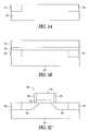
- FIGS. 5A-5Eillustrate an embodiment of a process for forming a metal substituted electrode in place of a previously deposited material on a dielectric containing TaSiON. Though a transistor is discussed with reference to FIGS. 5A-5E , such a process may be used with respect to other embodiments of device configurations.
- FIG. 5Ashows a substrate 501 and shallow trench isolation (STI) regions 502 .
- the substrate 501can be a semiconductor wafer as well as structures having one or more insulative, semi-insulative, conductive, or semiconductive layers and materials.
- the substratecan include silicon-on-insulator, silicon-on-sapphire, and other structures upon which semiconductor devices are formed.
- FIG. 5Bfurther shows a gate dielectric layer 503 formed on the substrate 501 , and a gate substitutable layer 504 formed on the gate dielectric layer 503 .
- the gate dielectric layermay include a dielectric layer containing TaSiON in addition to other insulative material or a dielectric layer essentially of TaSiON. The use of such a high-K dielectric increases the capacitance, which is useful for nanoscale integrated circuits.
- the gate dielectricincludes stacked layers comprising one or more high- ⁇ dielectric materials.
- the material of the gate substitutable layer 504is selected with respect to the desired gate material to allow the gate material to replace the gate substitutable layer. This process forms a gate of the desired gate metal where the substitutable material was positioned on the gate dielectric.
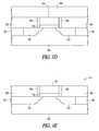
- Source/drain regions 507are also formed. Source/drain regions 507 can be formed using conventional ion implantation and subsequent annealing. These annealing temperatures can pose problems for aluminum gates and other metal gates that have melting temperatures less than the anneal temperature for the source/drain regions.
- FIG. 5Dshows an insulative fill layer 508 provided to match the thickness of the gate stack.
- a planarization proceduresuch as chemical-mechanical polishing, can be used to provide an even surface across the fill layer 508 and the gate substitutable layer 504 .
- a metal layer 509formed of material intended to be the gate material, is deposited over the gate substitutable layer 504 and the fill layer 508 .
- the metal layer 509is also referred to herein as a layer of gate material.
- Various deposition processessuch as evaporation, sputtering, chemical vapor deposition, or atomic layer deposition, may be used to form the metal layer 509 .
- the volume of layer 509is significantly larger than the volume of the substitutable material left on the wafer.
- a metal-substitution reactionis induced.
- the reactioncan be provided by annealing the structure in a non-oxidizing atmosphere such as a nitrogen gas or a forming gas. The heating urges diffusion or dissolution of the intended gate material in metal layer 509 for the substitutable material 504 .
- the substitution processis bounded by the spacers 506 and the gate dielectric 503 .
- FIG. 5Eshows the resulting low-resistance gate structure.
- the illustrated structureincludes a metal substituted gate 510 formed by the substitution of the metal of layer 509 .
- the metal substituted gate 510may include a small amount of the gate substitutable material that did not diffuse above the planarization level 511 . Such small amounts of the gate substitutable material do not significantly affect the conductivity of the metal substituted gate 510 , and thus do not significantly affect the performance of the device.
- Drain and source contactscan be formed, as well as interconnects to other transistors or components, using conventional techniques. Another heat treatment may occur after packaging the integrated circuit in a protective housing in an attempt to minimize the resistivity of the metal gate contacts and other metal interconnections.
- the metal gate substitution techniquecan be applied to MOS devices, as generally illustrated in FIG. 5E , as well as to form metal floating gates and/or metal control gates in nonvolatile devices. Additionally, various high- ⁇ dielectrics having a TaSiON film can be used between the floating gate and the substrate, and between the control gate and the floating gate in these nonvolatile devices.
- FIG. 6illustrates a flow diagram of features of an embodiment of a metal substitution technique.
- a gate dielectricis formed on a substrate.
- the gate dielectricincludes a TaSiON film.
- a layer of gate substitutable materialis formed on the gate dielectric. Examples of gate substitutable material include polysilicon, germanium, silicon-germanium, and carbon.
- source/drain regionsare formed.
- a layer of gate materialis formed at 615 on the gate substitutable material. Examples of such metals include gold, silver, and aluminum. Other metals may be used.
- the gate materialis substituted for the layer of gate substitutable material.
- a metal substitution reactionsubstitutes or replaces the substitutable material (e.g. silicon, germanium, silicon-germanium, carbon) with a metal. After the substitution, the resulting gate structure includes substantially all of the desired metal. Small amounts of the substitutable material may remain in the gate structure.
- the substitution reactioncan be induced by heating the integrated circuit assembly to a desired temperature in a vacuum, nitrogen, argon, forming gas or other non-oxidizing atmosphere. Heating causes diffusion of the metal layer 509 into the substitutable layer.
- the annealing temperature for the substitutionis less than the eutectic (lowest melting) temperature of materials involved in the substitution for the reaction for substitution to occur.
- a metal layermay be formed from gold and annealed at approximately 300° C.
- a metal layermay be formed from silver and annealed at approximately 500-600° C. to substitute the silver for a silicon substitutable structure.
- a polysilicon and germanium substitutable materialmay be used, which reduces the anneal temperature.
- the gate substitutable material 504 shown in FIGS. 5A-5Eincludes polysilicon.
- the gate substitutable materialincludes germanium.
- Some embodimentsuse silicon-germanium with a percentage of silicon in the range from 0% to 100% as the gate substitutable material 504 .
- Some embodimentsuse carbon as the gate substitutable material 504 .
- a replacement metal for the substituted gatemay include aluminium, silver, gold, an alloy of silver, an alloy of gold as the replacement metal, or combinations thereof.
- a replacement metal for the substituted gatemay include gold, silver, an alloy of gold, an alloy of silver, copper, platinum, rhenium, ruthenium, rhodium, nickel, osmium, palladium, iridium, cobalt, germanium, or combinations thereof.
- Various embodimentsform an integrated circuit structure using two or more substitution reactions. Relatively higher temperature substitution processes can be performed before relatively lower temperature substitution processes.
- One application for multiple substitution reactionsis to independently adjust work functions of NMOS and PMOS transistors in CMOS integrated circuits. Multiple substitution reactions are not limited to this CMOS integrated circuit application. Additional information regarding metal substitution can be found in U.S. patent application Ser. No. 11/176,738 filed Jul. 7, 2005, entitled “METAL-SUBSTITUTED TRANSISTOR GATES,” which is herein incorporated by reference.
- FIGS. 7A-7Dillustrate an embodiment of a process for forming a self aligned conductive layer such as a metal gate for a transistor structure.
- FIG. 7Aillustrates a high- ⁇ gate dielectric 710 containing TaSiON formed on a substrate 701 .
- the substrate 701can be a semiconductor wafer as well as structures having one or more insulative, semi-insulative, conductive, or semiconductive layers and materials.
- the substratecan include silicon-on-insulator, silicon-on-sapphire, and other structures upon which semiconductor devices are formed.
- a sacrificial gate 703is formed of amorphous carbon on the high- ⁇ gate dielectric 710 .
- an etch barrier 708is formed over the sacrificial gate and the dielectric.
- the etch barrier 708includes silicon nitride or aluminum oxide, and can be formed using a deposition process, according to various embodiments.
- Sacrificial sidewall spacers 706are added adjacent the sacrificial gate 703 .
- the spacers 706are formed of amorphous carbon by deposition and conventional direct etch techniques.
- An ion implantation 730 and high temperature annealare used to form source/drain regions 702 in areas defined by the sacrificial sidewall spacers 706 . These annealing temperatures can pose problems for aluminum gates and other metal gates that have melting temperatures less than the anneal temperature for the source/drain regions.
- FIG. 7Bthe sacrificial sidewall spacers ( 706 in FIG. 7A ) have been removed.
- Various embodimentsuse a plasma oxidation process to remove the sacrificial sidewall spacers.
- the etch barrier ( 708 in FIG. 7A )has been removed.
- a light dose ion implantation 740is used to form source/drain extensions 742 in the substrate 701 .
- the extensions 742can be annealed at lower temperatures and in shorter times than the more heavily doped source/drain regions 702 .
- source/drain extensions for the transistormay be formed with doping the substrate to a depth of 30 nm or less.
- conventional or non-carbon sidewall spacers 756are formed and the whole structure is back filled with an oxide fill 758 , such as silicon dioxide, and planarized.
- oxide fill 758such as silicon dioxide
- the conventional sidewall spacersare formed with silicon nitride.
- the sacrificial gate( 703 in FIG. 7C ) is removed and replaced by the deposition of a metal layer 760 .
- the sacrificial gateis removed using a plasma oxidation process.
- Various deposition processessuch as evaporation, sputtering, chemical vapor deposition, or atomic layer deposition, may be used to form the metal layer 760 .
- the structureis planarized (not shown) using a planarization procedure, such as chemical-mechanical polishing, resulting in the self aligned metal gate over the high- ⁇ gate dielectric insulator 710 .
- Drain and source contacts(not shown) can be formed, as well as interconnects to other transistors or components, using conventional techniques. Another heat treatment may occur after packaging the integrated circuit in a protective housing in an attempt to minimize the resistivity of the metal gate contacts and other metal interconnections.
- FIGS. 7A-7Dillustrate two replacement processes for the formation of planar self aligned metal gate transistors, one for disposable sidewall spacers and the other for the gate material itself.
- the metal gate replacement techniqueas disclosed herein, can be applied to MOS devices, as generally illustrated in FIGS. 7A-7D , as well as to form metal floating gates and/or metal control gates in nonvolatile devices. Additionally, various high- ⁇ dielectrics can be used between the floating gate and the substrate, and between the control gate and the floating gate in these nonvolatile devices.
- FIG. 8illustrates an embodiment of a method 800 for forming a self aligned metal gate on high- ⁇ gate dielectrics containing TaSiON.
- a high- ⁇ gate dielectric containing TaSiONis formed on a substrate, at 802 .
- a sacrificial carbon gateis formed on the gate dielectric.
- sacrificial carbon sidewall spacersare formed adjacent to the sacrificial carbon gate.
- source/drain regions for the transistorare formed, using the sacrificial carbon sidewall spacers to define the source/drain regions.
- the sacrificial carbon sidewall spacersare replaced with non-carbon sidewall spacers at 810 .
- the sacrificial carbon gateis replaced with a desired metal gate material to provide the desired metal gate material on the gate dielectric.
- source/drain extensionsmay be formed after removing the carbon sidewall spacers and before replacing with non-carbon sidewall spacers.
- An etch barrieris used in various embodiments to separate the sacrificial carbon gate from the sacrificial carbon sidewall spacers.
- the carbon sacrificial gatemay be replaced with aluminum (Al), tungsten (W), molybdenum (Mo), gold (Au), silver (Ag), gold alloy, silver alloy, copper (Cu), platinum (Pt), rhenium (Re), ruthenium (Ru), rhodium (Rh), nickel (Ni), osmium (Os), palladium (Pd), iridium (Ir), cobalt (Co), germanium (Ge), or metallic nitrides such as WN, TiN or TaN covered by metals.
- the high- ⁇ gate dielectric formed at 802may be one of a number of high- ⁇ gate dielectrics containing TaSiON.
- construction of an integrated circuit structureincludes a dielectric containing TaSiON on which is disposed a self-aligned metal electrode. Additional information regarding a self-aligned metal electrode used as a transistor gate can be found in U.S. patent application Ser. No. 11/216,375, filed 31 Aug. 2005, entitled “SELF ALIGNED METAL GATES ON HIGH- ⁇ DIELECTRICS,” which is herein incorporated by reference.
- FIG. 9illustrates an embodiment of a wafer 940 containing integrated circuits having one or more dielectric layers that include a tantalum silicon oxynitride film.
- Conductive electrodesmay be disposed on such dielectrics in a number of configurations such as capacitors, transistors, or elements of a memory.
- the conductive electrodesmay be metal electrodes, conductive metal nitride electrodes, and/or conductive metal oxide electrodes.
- the conductive electrodesmay be atomic layer deposited electrodes.
- Metal electrodesmay be metal substituted electrodes and/or self aligned metal electrodes formed in accordance with the teachings of embodiments discussed herein.
- a common wafer sizeis 8 inches in diameter.
- wafersare capable of being fabricated in other sizes, and embodiments of wafers containing a tantalum silicon oxynitride film are not limited to a particular size.
- a number of diescan be formed on a wafer.
- a die 941is an individual pattern on a substrate that contains circuitry to perform a specific function.
- a semiconductor wafertypically contains a repeated pattern of such dies containing the same functionality.
- a dieis typically packaged in a protective casing (not shown) with leads extending therefrom (not shown) providing access to the circuitry of the die for communication and control.
- Applications containing electronic devices having dielectric layers containing tantalum silicon oxynitride filminclude electronic systems for use in memory modules, device drivers, power modules, communication modems, processor modules, and application-specific modules, which may include multilayer, multichip modules.
- Such dielectric layersmay be configured as multiple layers containing at least one layer of TaSiON or configured substantially as a TaSiON layer.
- such dielectric layersmay be configured in contact with a metal electrode.
- Such circuitrycan be a subcomponent of a variety of electronic systems, such as a clock, a television, a cell phone, a personal computer, an automobile, an industrial control system, an aircraft, and others.
- FIG. 10shows an embodiment of a transistor 1000 having a dielectric layer 1040 containing a TaSiON x film.
- transistor 1000includes a source region 1020 and a drain region 1030 in a silicon-based substrate 1010 where source and drain regions 1020 , 1030 are separated by a body region 1032 .
- Body region 1032defines a channel having a channel length 1034 .
- a gate dielectric 1040is disposed on substrate 1010 with gate dielectric 1040 formed as a dielectric layer containing TaSiON x .
- gate dielectric 1040is realized as a dielectric layer formed substantially of TaSiON x .
- gate dielectric 1040is constructed as multiple dielectric layers, that is, as a dielectric stack, containing at least one TaSiON x film and one or more layers of insulating material other than tantalum silicon oxynitride film.
- the TaSiON x filmis structured as one or more monolayers.
- An embodiment of a TaSiON x filmis formed using atomic layer deposition.
- gate dielectric 1040may be realized as a gate insulator in a silicon-based structure.
- a gate 1050is formed on and contacts gate dielectric 1040 .
- gate 1050includes conductive material.
- gate 1050includes a conductive material structured as one or more monolayers.
- the conductive material layeris an ALD conductive material layer.
- the conductive material layeris a substituted metal layer.
- the conductive material layeris a self-aligned metal layer.
- the thickness of the conductive layerranges from a monolayer to thousands of angstroms or more.
- An interfacial layermay form between body region 1032 and gate a dielectric 1040 .
- an interfacial layeris limited to a relatively small thickness compared to gate dielectric 1040 , or to a thickness significantly less than gate dielectric 1040 as to be effectively eliminated.
- forming the substrate and the source and drain regionsis performed using standard processes known to those skilled in the art.
- the sequencing of the various elements of the process for forming a transistoris conducted with fabrication processes known to those skilled in the art.
- transistor 1000is a MOSFET transistor.
- transistor 1000is a germanium MOSFET structure.
- transistor 1000is a silicon MOSFET structure.
- transistor 1000is a silicon-germanium (SiGe) MOSFET structure. In an embodiment, transistor 1000 is a gallium arsenide MOSFET structure. In an embodiment, transistor 1000 is a NMOS transistor. In an embodiment, transistor 1000 is a PMOS transistor. Transistor 1000 is not limited to the arrangement illustrated in FIG. 10 . For example, transistor 1000 may be structured as a vertical transistor. In an embodiment, use of a gate dielectric containing tantalum silicon oxynitride is not limited to silicon-based substrates, but is used with a variety of semiconductor substrates.
- FIG. 11shows an embodiment of a floating gate transistor 1100 having a dielectric layer containing a TaSiON x film.
- the TaSiON x filmis structured as one or more monolayers.
- the TaSiON x filmis formed using atomic layer deposition techniques.
- transistor 1100includes a silicon-based substrate 1110 with a source 1120 and a drain 1130 separated by a body region 1132 . Body region 1132 between source 1120 and drain 1130 defines a channel region having a channel length 1134 .
- a stack 1155including a gate dielectric 1140 , a floating gate 1152 , a floating gate dielectric 1142 (integrate dielectric 1142 ), and a control gate 1150 .
- An interfacial layermay form between body region 1132 and gate dielectric 1140 . In an embodiment, such an interfacial layer is limited to a relatively small thickness compared to gate dielectric 1140 , or to a thickness significantly less than gate dielectric 1140 as to be effectively eliminated.
- gate dielectric 1140includes a dielectric containing an atomic layer deposited TaSiON x film formed in embodiments similar to those described herein. In an embodiment, gate dielectric 1140 is realized as a dielectric layer formed substantially of TaSiON x . In an embodiment, gate dielectric 1140 is a dielectric stack containing at least one TaSiON x film and one or more layers of other insulating materials.
- floating gate 1152is formed on and contacts gate dielectric 1140 .
- floating gate 1152includes conductive material.
- floating gate 1152is structured as one or more monolayers.
- floating gate 1152is an ALD layer.
- floating gate 1152is a substituted metal layer.
- floating gate 1152is a self-aligned metal layer.
- the thickness of the floating gate layerranges from a monolayer to thousands of angstroms or more.
- floating gate dielectric 1142includes a dielectric containing a TaSiON x film.
- the TaSiON x filmis structured as one or more monolayers.
- the TaSiON xis formed using atomic layer deposition techniques.
- floating gate dielectric 1142is realized as a dielectric layer formed substantially of TaSiON x .
- floating gate dielectric 1142is a dielectric stack containing at least one TaSiON x film and one or more layers of other insulating materials.
- control gate 1150is formed on and contacts floating gate dielectric 1142 .
- control gate 1150includes conductive material.
- control gate 1150is structured as one or more monolayers.
- the control gate 1150is an ALD layer.
- control gate 1150is a substituted metal layer.
- control gate 1150is a self-aligned metal layer.
- the thickness of the control gate layer 1150ranges from a monolayer to thousands of angstroms or more.
- control gate 1150is structured as one or more monolayers.
- both gate dielectric 1140 and floating gate dielectric 1142are formed as dielectric layers containing a TaSiON x film structured as one or more monolayers.
- control gate 1150 and floating gate 1152are formed as conductive layers.
- the control gate 1150 and floating gate 1152are structured as one or more monolayers.
- control gate 1150 and floating gate 1152are ALD layers.
- control gate 1150 and floating gate 1152are substituted metal layers.
- control gate 1150 and floating gate 1152are self-aligned metal layers.
- gate dielectric 1140 , floating gate dielectric 1142 , control gate 1150 , and floating gate 1152are realized by embodiments similar to those described herein, with the remaining elements of the transistor 1100 formed using processes known to those skilled in the art.
- gate dielectric 1140forms a tunnel gate insulator and floating gate dielectric 1142 forms an inter-gate insulator in flash memory devices, where gate dielectric 1140 and floating gate dielectric 1142 may include an tantalum silicon oxynitride film structured as one or more monolayers.
- Floating gate transistor 1100is not limited to the arrangement illustrated in FIG. 11 .
- floating gate transistor 1100may be structured as a vertical transistor. Such structures are not limited to silicon-based substrates, but may be used with a variety of semiconductor substrates, such as for but not limited to germanium floating gate transistors, SiGe floating gate transistors, and gallium arsenide floating gate transistors.
- FIG. 12shows an embodiment of a capacitor 1200 having a dielectric layer containing a tantalum silicon oxynitride film 1220 and having an electrode 1230 .
- Embodiments of a tantalum silicon oxynitride film 1220 structured as one or more monolayersmay also be applied to capacitors in various integrated circuits, memory devices, and electronic systems.
- a methodincludes forming a first conductive layer 1210 , forming a dielectric layer 1220 containing a tantalum silicon oxynitride film structured as one or more monolayers on first conductive layer 1210 , and forming a second conductive layer 1230 on dielectric layer 1220 .
- second conductive layer 1230 , first conductive layer 1210 , or both second and first conductive layers 1230 , 1210are ALD conductive material layers, substituted metal layers, self-aligned metal layers, or a combination thereof.
- the thickness of the conductive layerranges from a monolayer to thousands of angstroms or more.
- dielectric layer 1220containing a TaSiON x film, and conductive layers 1210 , 1220 are formed using various embodiments described herein.
- dielectric layer 1220is realized as a dielectric layer formed substantially of TaSiON x .
- dielectric layer 1220is a dielectric stack containing at least one TaSiON x film and one or more layers of other insulating materials.
- Embodiments for a tantalum silicon oxynitride filmmay include, but are not limited to, a capacitor in a DRAM and capacitors in analog, radio frequency (RF), and mixed signal integrated circuits. Mixed signal integrated circuits are integrated circuits that may operate with digital and analog signals.
- RFradio frequency
- FIG. 13depicts an embodiment of a dielectric structure 1300 having multiple dielectric layers 1305 - 1 , 1305 - 2 . . . 1305 -N, in which at least one layer is a tantalum silicon oxynitride layer.
- layers 1310 and 1320provide means to contact dielectric layers 1305 - 1 , 1305 - 2 . . . 1305 -N.
- each layer 1310 , 1320 or both layersare conductive layers.
- layers 1310 and 1320are electrodes forming a capacitor.
- layer 1310is a body region of a transistor with layer 1320 being a gate.
- layer 1310is a floating gate electrode with layer 1320 being a control gate.
- dielectric structure 1300includes one or more layers 1305 - 1 , 1305 - 2 . . . 1305 -N as dielectric layers other than a TaSiON layer, where at least one layer is a TaSiON layer.
- dielectric layers 1305 - 1 , 1305 - 2 . . . 1305 -Ninclude a SiO layer, a SiN layer, a TaO layer, a TaN layer, a SiON layer, a TaON layer, or various combinations of these layers.
- dielectric layers 1305 - 1 , 1305 - 2 . . . 1305 -Ninclude an insulating metal oxide layer.
- dielectric layers 1305 - 1 , 1305 - 2 . . . 1305 -Ninclude an insulating nitride layer. In an embodiment, dielectric layers 1305 - 1 , 1305 - 2 . . . 1305 -N include an insulating oxynitride layer. In an embodiment, dielectric layers 1305 - 1 , 1305 - 2 . . . 1305 -N include an insulating silicate layer.
- a dielectric layer containing a tantalum silicon oxynitride film structured as one or more monolayersmay provide for enhanced device performance by providing devices with reduced leakage current. Such improvements in leakage current characteristics may be attained by forming one or more layers of a tantalum silicon oxynitride in a nanolaminate structure with other metal oxides, non-metal-containing dielectrics, or combinations thereof. The transition from one layer of the nanolaminate to another layer of the nanolaminate provides disruption to a tendency for an ordered structure in the nanolaminate stack.
- nanolaminatemeans a composite film of ultra thin layers of two or more materials in a layered stack.
- each layer in a nanolaminatehas a thickness of an order of magnitude in the nanometer range.
- each individual material layer of the nanolaminatemay have a thickness as low as a monolayer of the material or as high as 20 nanometers.
- a SiO/TaSiON nanolaminatecontains alternating layers of a SiO and TaSiON.
- a SiN/TaSiON nanolaminatecontains alternating layers of a SiN and TaSiON.
- a SiON/TaSiON nanolaminatecontains alternating layers of a SiON and TaSiON.
- a TaON/TaSiON nanolaminatecontains alternating layers of TaON and TaSiON. In an embodiment, a TaO/TaSiON nanolaminate contains alternating layers of TaO and TaSiON. In an embodiment, a TaN/TaSiON nanolaminate contains alternating layers of TaN and TaSiON.
- a SiO/SiON/TaON/TaO/TaN/SiN/TaSiON nanolaminatecontains various permutations of silicon oxide layers, silicon oxynitride layers, tantalum oxynitride layers, tantalum oxide layers, tantalum nitride layers, silicon nitride layers, and tantalum silicon oxynitride layers.
- the sequencing of the layers in dielectric structure 1300 structured as a nanolaminatedepends on the application.
- the effective dielectric constant associated with nanolaminate structure 1300is that attributable to N capacitors in series, where each capacitor has a thickness defined by the thickness and composition of the corresponding layer.
- a nanolaminate structureis engineered to have a predetermined dielectric constant.
- Embodiments for structures such as nanolaminate structure 1300may be used as nanolaminate dielectrics in flash memory devices as well as other integrated circuits.
- a layer of the nanolaminate structure 1300is used to store charge in a flash memory device.
- the charge storage layer of a nanolaminate structure 1300 in a flash memory devicemay be a silicon oxide layer.
- transistors, capacitors, and other devicesinclude dielectric films containing a layer of a tantalum silicon oxynitride composition with an electrode.
- the tantalum silicon oxynitride layeris an atomic layer deposited tantalum silicon oxynitride layer.
- the electrodeis an atomic layer deposited electrode.
- the electrodeis a substituted metal layer.
- the electrodeis a self-aligned metal layer.
- dielectric films containing a tantalum silicon oxynitride layer with an electrodeare implemented into memory devices and electronic systems including information handling devices.
- information handling devicesinclude wireless systems, telecommunication systems, and computers. In various embodiments, such electronic devices and electronic apparatus are realized as integrated circuits.
- FIG. 14illustrates a block diagram for an electronic system 1400 with one or more devices having a dielectric structure including a TaSiON x film with an electrode.
- Electronic system 1400includes a controller 1405 , a bus 1415 , and an electronic device 1425 , where bus 1415 provides electrical conductivity between controller 1405 and electronic device 1425 .
- controller 1405includes an embodiment of a TaSiON x film with an electrode.
- electronic device 1425includes an embodiment of a TaSiON x film with an electrode.
- controller 1405 and electronic device 1425include embodiments of a TaSiON x film with an electrode.
- electronic system 1400includes, but is not limited to, fiber optic systems, electro-optic systems, and information handling systems such as wireless systems, telecommunication systems, and computers.
- FIG. 15depicts a diagram of an embodiment of a system 1500 having a controller 1505 and a memory 1525 .
- controller 1505includes a TaSiON film with an electrode.
- memory 1525includes a TaSiON film structured as one or more monolayers with an electrode.
- controller 1505 and memory 1525each include a TaSiON film with an electrode.
- system 1500also includes an electronic apparatus 1535 and a bus 1515 , where bus 1515 provides electrical conductivity between controller 1505 and electronic apparatus 1535 and between controller 1505 and memory 1525 .
- bus 1515includes an address bus, a data bus, and a control bus, each independently configured.
- bus 1515uses common conductive lines for providing one or more of address, data, or control, the use of which is regulated by controller 1505 .
- electronic apparatus 1535is additional memory configured in a manner similar to memory 1525 .
- additional peripheral device or devices 1545are coupled to bus 1515 .
- peripheral devices 1545include displays, additional storage memory, or other control devices that may operate in conjunction with controller 1505 .
- peripheral devices 1545may include displays, additional storage memory, or other control devices that may operate in conjunction with memory 1525 , or controller 1505 and memory 1525 .
- controller 1505is a processor.
- controller 1505includes an embodiment of a dielectric layer having a TaSiON film structured as one or more monolayers with an electrode.
- system 1500includes, but is not limited to, information handling devices, telecommunication systems, and computers.
- memory 1525is realized as a memory device containing a TaSiON film structured as one or more monolayers with an electrode.
- a TaSiON structure with a conductive layeris formed in a memory cell of a memory array.
- such a structureis formed in a capacitor in a memory cell of a memory array.
- such a structureis formed in a transistor in a memory cell of a memory array.
- Memory typesinclude a DRAM, SRAM (Static Random Access Memory) or Flash memories.
- the DRAMcould be a synchronous DRAM commonly referred to as SGRAM (Synchronous Graphics Random Access Memory), SDRAM (Synchronous Dynamic Random Access Memory), SDRAM II, and DDR SDRAM (Double Data Rate SDRAM), as well as other emerging DRAM technologies.
- SGRAMSynchronous Graphics Random Access Memory
- SDRAMSynchronous Dynamic Random Access Memory
- SDRAM IISynchronous Dynamic Random Access Memory
- DDR SDRAMDouble Data Rate SDRAM
Landscapes
- Engineering & Computer Science (AREA)
- Chemical & Material Sciences (AREA)
- Manufacturing & Machinery (AREA)
- General Physics & Mathematics (AREA)
- Physics & Mathematics (AREA)
- Computer Hardware Design (AREA)
- Microelectronics & Electronic Packaging (AREA)
- Power Engineering (AREA)
- Condensed Matter Physics & Semiconductors (AREA)
- Chemical Kinetics & Catalysis (AREA)
- General Chemical & Material Sciences (AREA)
- Inorganic Chemistry (AREA)
- Materials Engineering (AREA)
- Mechanical Engineering (AREA)
- Metallurgy (AREA)
- Organic Chemistry (AREA)
- Formation Of Insulating Films (AREA)
- Semiconductor Memories (AREA)
- Insulated Gate Type Field-Effect Transistor (AREA)
Abstract
Description
Claims (40)
Priority Applications (3)
| Application Number | Priority Date | Filing Date | Title |
|---|---|---|---|
| US11/514,601US7776765B2 (en) | 2006-08-31 | 2006-08-31 | Tantalum silicon oxynitride high-k dielectrics and metal gates |
| US12/855,556US8168502B2 (en) | 2006-08-31 | 2010-08-12 | Tantalum silicon oxynitride high-K dielectrics and metal gates |
| US13/458,196US8519466B2 (en) | 2006-08-31 | 2012-04-27 | Tantalum silicon oxynitride high-K dielectrics and metal gates |
Applications Claiming Priority (1)
| Application Number | Priority Date | Filing Date | Title |
|---|---|---|---|
| US11/514,601US7776765B2 (en) | 2006-08-31 | 2006-08-31 | Tantalum silicon oxynitride high-k dielectrics and metal gates |
Related Child Applications (1)
| Application Number | Title | Priority Date | Filing Date |
|---|---|---|---|
| US12/855,556DivisionUS8168502B2 (en) | 2006-08-31 | 2010-08-12 | Tantalum silicon oxynitride high-K dielectrics and metal gates |
Publications (2)
| Publication Number | Publication Date |
|---|---|
| US20080057690A1 US20080057690A1 (en) | 2008-03-06 |
| US7776765B2true US7776765B2 (en) | 2010-08-17 |
Family
ID=39152215
Family Applications (3)
| Application Number | Title | Priority Date | Filing Date |
|---|---|---|---|
| US11/514,601Active2028-06-22US7776765B2 (en) | 2006-08-31 | 2006-08-31 | Tantalum silicon oxynitride high-k dielectrics and metal gates |
| US12/855,556ActiveUS8168502B2 (en) | 2006-08-31 | 2010-08-12 | Tantalum silicon oxynitride high-K dielectrics and metal gates |
| US13/458,196ActiveUS8519466B2 (en) | 2006-08-31 | 2012-04-27 | Tantalum silicon oxynitride high-K dielectrics and metal gates |
Family Applications After (2)
| Application Number | Title | Priority Date | Filing Date |
|---|---|---|---|
| US12/855,556ActiveUS8168502B2 (en) | 2006-08-31 | 2010-08-12 | Tantalum silicon oxynitride high-K dielectrics and metal gates |
| US13/458,196ActiveUS8519466B2 (en) | 2006-08-31 | 2012-04-27 | Tantalum silicon oxynitride high-K dielectrics and metal gates |
Country Status (1)
| Country | Link |
|---|---|
| US (3) | US7776765B2 (en) |
Cited By (6)
| Publication number | Priority date | Publication date | Assignee | Title |
|---|---|---|---|---|
| US20090194791A1 (en)* | 2006-09-29 | 2009-08-06 | Fujitsu Limited | Compound semiconductor device and manufacturing method thereof |
| US20090294924A1 (en)* | 2006-08-31 | 2009-12-03 | Leonard Forbes | Hafnium lanthanide oxynitride films |
| US7915174B2 (en) | 2004-12-13 | 2011-03-29 | Micron Technology, Inc. | Dielectric stack containing lanthanum and hafnium |
| US8084808B2 (en) | 2005-04-28 | 2011-12-27 | Micron Technology, Inc. | Zirconium silicon oxide films |
| US20130273727A1 (en)* | 2012-04-13 | 2013-10-17 | Jeonggil Lee | Semiconductor devices and methods for fabricating the same |
| US9627500B2 (en) | 2015-01-29 | 2017-04-18 | Samsung Electronics Co., Ltd. | Semiconductor device having work-function metal and method of forming the same |
Families Citing this family (38)
| Publication number | Priority date | Publication date | Assignee | Title |
|---|---|---|---|---|
| US7476925B2 (en) | 2001-08-30 | 2009-01-13 | Micron Technology, Inc. | Atomic layer deposition of metal oxide and/or low asymmetrical tunnel barrier interploy insulators |
| US7160577B2 (en) | 2002-05-02 | 2007-01-09 | Micron Technology, Inc. | Methods for atomic-layer deposition of aluminum oxides in integrated circuits |
| US7589029B2 (en) | 2002-05-02 | 2009-09-15 | Micron Technology, Inc. | Atomic layer deposition and conversion |
| US7135421B2 (en) | 2002-06-05 | 2006-11-14 | Micron Technology, Inc. | Atomic layer-deposited hafnium aluminum oxide |
| US7135369B2 (en) | 2003-03-31 | 2006-11-14 | Micron Technology, Inc. | Atomic layer deposited ZrAlxOy dielectric layers including Zr4AlO9 |
| US7601649B2 (en) | 2004-08-02 | 2009-10-13 | Micron Technology, Inc. | Zirconium-doped tantalum oxide films |
| US7081421B2 (en) | 2004-08-26 | 2006-07-25 | Micron Technology, Inc. | Lanthanide oxide dielectric layer |
| US7588988B2 (en) | 2004-08-31 | 2009-09-15 | Micron Technology, Inc. | Method of forming apparatus having oxide films formed using atomic layer deposition |
| US7494939B2 (en) | 2004-08-31 | 2009-02-24 | Micron Technology, Inc. | Methods for forming a lanthanum-metal oxide dielectric layer |
| US7374964B2 (en) | 2005-02-10 | 2008-05-20 | Micron Technology, Inc. | Atomic layer deposition of CeO2/Al2O3 films as gate dielectrics |
| US7687409B2 (en) | 2005-03-29 | 2010-03-30 | Micron Technology, Inc. | Atomic layer deposited titanium silicon oxide films |
| US7662729B2 (en) | 2005-04-28 | 2010-02-16 | Micron Technology, Inc. | Atomic layer deposition of a ruthenium layer to a lanthanide oxide dielectric layer |
| US7927948B2 (en) | 2005-07-20 | 2011-04-19 | Micron Technology, Inc. | Devices with nanocrystals and methods of formation |
| US7989290B2 (en)* | 2005-08-04 | 2011-08-02 | Micron Technology, Inc. | Methods for forming rhodium-based charge traps and apparatus including rhodium-based charge traps |
| US7575978B2 (en) | 2005-08-04 | 2009-08-18 | Micron Technology, Inc. | Method for making conductive nanoparticle charge storage element |
| US7709402B2 (en) | 2006-02-16 | 2010-05-04 | Micron Technology, Inc. | Conductive layers for hafnium silicon oxynitride films |
| US7544604B2 (en) | 2006-08-31 | 2009-06-09 | Micron Technology, Inc. | Tantalum lanthanide oxynitride films |
| US7605030B2 (en) | 2006-08-31 | 2009-10-20 | Micron Technology, Inc. | Hafnium tantalum oxynitride high-k dielectric and metal gates |
| US7759747B2 (en) | 2006-08-31 | 2010-07-20 | Micron Technology, Inc. | Tantalum aluminum oxynitride high-κ dielectric |
| US7776765B2 (en) | 2006-08-31 | 2010-08-17 | Micron Technology, Inc. | Tantalum silicon oxynitride high-k dielectrics and metal gates |
| US20080087890A1 (en)* | 2006-10-16 | 2008-04-17 | Micron Technology, Inc. | Methods to form dielectric structures in semiconductor devices and resulting devices |
| US7898850B2 (en)* | 2007-10-12 | 2011-03-01 | Micron Technology, Inc. | Memory cells, electronic systems, methods of forming memory cells, and methods of programming memory cells |
| US7759715B2 (en)* | 2007-10-15 | 2010-07-20 | Micron Technology, Inc. | Memory cell comprising dynamic random access memory (DRAM) nanoparticles and nonvolatile memory (NVM) nanoparticle |
| US8692310B2 (en) | 2009-02-09 | 2014-04-08 | Spansion Llc | Gate fringing effect based channel formation for semiconductor device |
| KR101584100B1 (en)* | 2009-10-29 | 2016-01-13 | 삼성전자주식회사 | Method of forming metal silicate film and method of forming semiconductor device using the same |
| US20120064682A1 (en)* | 2010-09-14 | 2012-03-15 | Jang Kyung-Tae | Methods of Manufacturing Three-Dimensional Semiconductor Memory Devices |
| KR101757454B1 (en)* | 2010-10-21 | 2017-07-27 | 삼성전자주식회사 | A method for forming a three dimensional non-volatile memory device |
| WO2012057889A1 (en)* | 2010-10-29 | 2012-05-03 | Applied Materials, Inc. | Atomic layer deposition film with tunable refractive index and absorption coefficient and methods of making |
| KR20120107762A (en)* | 2011-03-22 | 2012-10-04 | 삼성전자주식회사 | Methods of fabricating semiconductor devices |
| US8518811B2 (en) | 2011-04-08 | 2013-08-27 | Infineon Technologies Ag | Schottky diodes having metal gate electrodes and methods of formation thereof |
| US8822283B2 (en) | 2011-09-02 | 2014-09-02 | Taiwan Semiconductor Manufacturing Company, Ltd. | Self-aligned insulated film for high-k metal gate device |
| US8975706B2 (en)* | 2013-08-06 | 2015-03-10 | Intermolecular, Inc. | Gate stacks including TaXSiYO for MOSFETS |
| US20150214331A1 (en)* | 2014-01-30 | 2015-07-30 | Globalfoundries Inc. | Replacement metal gate including dielectric gate material |
| KR20180032678A (en)* | 2015-08-21 | 2018-03-30 | 어플라이드 머티어리얼스, 인코포레이티드 | High temperature thermal ALD silicon nitride films |
| TWI807195B (en)* | 2019-06-28 | 2023-07-01 | 美商應用材料股份有限公司 | Fluorine-doped nitride films for improved high-k reliability |
| KR102138149B1 (en)* | 2019-08-29 | 2020-07-27 | 솔브레인 주식회사 | Growth inhibitor for forming thin film, method for forming thin film and semiconductor substrate prepared therefrom |
| US11725280B2 (en)* | 2020-08-26 | 2023-08-15 | Asm Ip Holding B.V. | Method for forming metal silicon oxide and metal silicon oxynitride layers |
| US11855140B2 (en)* | 2020-09-29 | 2023-12-26 | Taiwan Semiconductor Manufacturing Co., Ltd. | Gate oxide of nanostructure transistor with increased corner thickness |
Citations (276)
| Publication number | Priority date | Publication date | Assignee | Title |
|---|---|---|---|---|
| US4542870A (en) | 1983-08-08 | 1985-09-24 | The United States Of America As Represented By The Secretary Of The Army | SSICM guidance and control concept |
| US5252370A (en) | 1991-04-23 | 1993-10-12 | Tdk Corporation | Optical recording medium and method for making |
| US5334433A (en) | 1992-12-28 | 1994-08-02 | Tdk Corporation | Optical recording medium |
| US5364708A (en) | 1991-02-20 | 1994-11-15 | Tdk Corporation | Optical recording medium |
| US5401609A (en) | 1991-12-13 | 1995-03-28 | Tdk Corporation | Optical recording medium and its production |
| US5406546A (en) | 1992-10-05 | 1995-04-11 | Tdk Corporation | Magneto-optical disk |
| US5418030A (en) | 1992-06-12 | 1995-05-23 | Tdk Corporation | Optical recording medium and method for making |
| US5430706A (en) | 1993-04-16 | 1995-07-04 | Tdk Corporation | Magneto-optical disk having lands and grooves for recording information |
| US5470628A (en) | 1993-12-13 | 1995-11-28 | Tdk Corporation | Optical recording medium |
| US5498507A (en) | 1994-03-29 | 1996-03-12 | Tdk Corporation | Optical recording media |
| US5523140A (en) | 1994-03-31 | 1996-06-04 | Tdk Corporation | Optical recording method and medium |
| US5552237A (en) | 1992-09-30 | 1996-09-03 | Tdk Corporation | Magnetooptical recording medium |
| US5569517A (en) | 1994-06-23 | 1996-10-29 | Tdk Corporation | Optical information medium |
| US5577020A (en) | 1993-10-08 | 1996-11-19 | Tdk Corporation | Magneto-optical disc with intermediate film layer between a recording film and a dielectric film |
| US5593789A (en) | 1993-12-14 | 1997-01-14 | Tdk Corporation | Magneto-optical recording medium |
| US5620766A (en) | 1992-06-29 | 1997-04-15 | Tdk Corporation | Magneto-optical disk |
| US5627012A (en) | 1995-02-13 | 1997-05-06 | Tdk Corporation | Method for preparing phase change optical recording medium |
| US5637371A (en) | 1995-02-21 | 1997-06-10 | Tdk Corporation | Phase change optical recording medium and activation energy determining method |
| US5637372A (en) | 1995-03-31 | 1997-06-10 | Tdk Corporation | Phase change optical recording medium |
| US5700567A (en) | 1991-03-14 | 1997-12-23 | Tdk Corporation | Magneto-optical recording medium |
| US5825046A (en) | 1996-10-28 | 1998-10-20 | Energy Conversion Devices, Inc. | Composite memory material comprising a mixture of phase-change memory material and dielectric material |
| US5891542A (en) | 1996-12-10 | 1999-04-06 | Tdk Corporation | Optical recording material, and optical recording medium |
| US5906874A (en) | 1996-12-28 | 1999-05-25 | Tdk Corporation | Optical recording medium, and its fabrication method |
| US5965323A (en) | 1997-02-27 | 1999-10-12 | Tdk Corporation | Method for preparing optical recording medium |
| US5981014A (en) | 1997-05-29 | 1999-11-09 | Tdk Corporation | Optical recording medium and method for preparing the same |
| US5994240A (en) | 1996-07-03 | 1999-11-30 | Micron Technology, Inc. | Method for cleaning semiconductor wafers |
| US6002418A (en) | 1997-04-16 | 1999-12-14 | Fuji Photo Film Co., Ltd. | Thermal head |
| US6020024A (en) | 1997-08-04 | 2000-02-01 | Motorola, Inc. | Method for forming high dielectric constant metal oxides |
| US6030679A (en) | 1997-08-20 | 2000-02-29 | Tdk Corporation | Optical recording material and its fabrication method |
| US6040030A (en) | 1997-09-19 | 2000-03-21 | Tdk Corporation | Optical recording medium |
| US6051363A (en) | 1997-01-10 | 2000-04-18 | Tdkcorporation | Method for making an optical recording medium |
| US6061077A (en) | 1998-08-04 | 2000-05-09 | Fuji Photo Film Co., Ltd. | Thermal head |
| US6081287A (en) | 1997-04-22 | 2000-06-27 | Fuji Photo Film Co., Ltd. | Thermal head method of manufacturing the same |
| US6087674A (en) | 1996-10-28 | 2000-07-11 | Energy Conversion Devices, Inc. | Memory element with memory material comprising phase-change material and dielectric material |
| US6087067A (en) | 1997-04-10 | 2000-07-11 | Tdkcorporation | Optical recording medium |
| US6103330A (en) | 1997-05-26 | 2000-08-15 | Tdk Corporation | Optical recording medium and fabrication method therefor |
| US6137520A (en) | 1997-07-17 | 2000-10-24 | Fuji Photo Film Co., Ltd. | Thermal head |
| US6136168A (en) | 1993-01-21 | 2000-10-24 | Tdk Corporation | Clean transfer method and apparatus therefor |
| US6153355A (en) | 1997-06-27 | 2000-11-28 | Tdk Corporation | Optical recording medium and method for preparing the same |
| EP1096042A1 (en) | 1999-10-25 | 2001-05-02 | Motorola, Inc. | Method for fabricating a semiconductor structure including a metal oxide interface with silicon |
| US6242157B1 (en) | 1996-08-09 | 2001-06-05 | Tdk Corporation | Optical recording medium and method for making |
| US6243941B1 (en) | 1998-07-17 | 2001-06-12 | Fuji Photo Film Co., Ltd. | Thermal head fabrication method |
| US6256052B1 (en) | 1998-07-21 | 2001-07-03 | Fuji Photo Film Co., Ltd. | Thermal head |
| US6256053B1 (en) | 1999-03-25 | 2001-07-03 | Fuji Photo Film Co., Ltd. | Thermal head |
| EP1124262A2 (en) | 2000-02-11 | 2001-08-16 | Sharp Kabushiki Kaisha | Multilayer dielectric stack and method |
| US20010015441A1 (en) | 1999-12-10 | 2001-08-23 | Ritsuko Kawasaki | Semiconductor device and a method of manufacturing the same |
| US20010032995A1 (en) | 2000-01-19 | 2001-10-25 | Jon-Paul Maria | Lanthanum oxide-based gate dielectrics for integrated circuit field effect transistors and methods of fabricating same |
| US6316054B1 (en) | 1999-03-25 | 2001-11-13 | Fuji Photo Film Co., Ltd. | Carbon layer forming method |
| US6329036B1 (en) | 1998-12-09 | 2001-12-11 | Tdk Corporation | Optical recording medium and use |
| US20010054598A1 (en) | 2000-03-31 | 2001-12-27 | Makoto Kashiwaya | Method of fabricating thermal head |
| US6337704B1 (en) | 1997-04-14 | 2002-01-08 | Fuji Photo Film Co., Ltd. | Thermal head adjusting method |
| US6351276B1 (en) | 1998-05-21 | 2002-02-26 | Fuji Photo Film Co., Ltd. | Thermal recording apparatus |
| US6352591B1 (en) | 1996-11-13 | 2002-03-05 | Applied Materials, Inc. | Methods and apparatus for shallow trench isolation |
| US6358766B1 (en) | 1999-06-22 | 2002-03-19 | Semiconductor Energy Laboratory Co., Ltd. | Method of fabricating a semiconductor device |
| US6383873B1 (en) | 2000-05-18 | 2002-05-07 | Motorola, Inc. | Process for forming a structure |
| US6410368B1 (en) | 1999-10-26 | 2002-06-25 | Semiconductor Energy Laboratory Co., Ltd. | Method of manufacturing a semiconductor device with TFT |
| US20020089023A1 (en) | 2001-01-05 | 2002-07-11 | Motorola, Inc. | Low leakage current metal oxide-nitrides and method of fabricating same |
| US6426245B1 (en) | 1999-07-09 | 2002-07-30 | Semiconductor Energy Laboratory Co., Ltd. | Method for manufacturing a semiconductor device |
| US20020137330A1 (en) | 1999-10-01 | 2002-09-26 | Ryan Vivian W. | Process for fabricating copper interconnect for ULSI integrated circuits |
| US6461710B1 (en) | 1998-12-09 | 2002-10-08 | Tdk Corporation | Optical recording medium |
| US20020155689A1 (en) | 2001-04-20 | 2002-10-24 | Ahn Kie Y. | Highly reliable gate oxide and method of fabrication |
| US6492659B1 (en) | 1999-05-15 | 2002-12-10 | Semiconductor Energy Laboratory Co., Ltd. | Semiconductor device having single crystal grains with hydrogen and tapered gate insulation layer |
| US6495436B2 (en) | 2001-02-09 | 2002-12-17 | Micron Technology, Inc. | Formation of metal oxide gate dielectric |
| US6495449B1 (en)* | 2000-03-07 | 2002-12-17 | Simplus Systems Corporation | Multilayered diffusion barrier structure for improving adhesion property |
| US20020192974A1 (en) | 2001-06-13 | 2002-12-19 | Ahn Kie Y. | Dielectric layer forming method and devices formed therewith |
| US20030008235A1 (en) | 1999-02-15 | 2003-01-09 | Hiroyasu Inoue | Optical recording medium and method for its initialization |
| US20030016619A1 (en) | 2001-06-21 | 2003-01-23 | Judge John S. | Optical recording article |
| US20030017717A1 (en) | 2001-07-18 | 2003-01-23 | Ahn Kie Y. | Methods for forming dielectric materials and methods for forming semiconductor devices |
| US20030040196A1 (en) | 2001-08-27 | 2003-02-27 | Lim Jung Wook | Method of forming insulation layer in semiconductor devices for controlling the composition and the doping concentration |
| US20030045078A1 (en) | 2001-08-30 | 2003-03-06 | Micron Technology, Inc. | Highly reliable amorphous high-K gate oxide ZrO2 |
| US20030043637A1 (en) | 2001-08-30 | 2003-03-06 | Micron Technology, Inc | Flash memory with low tunnel barrier interpoly insulators |
| US20030060146A1 (en) | 1999-03-26 | 2003-03-27 | Makoto Kashiwaya | Thermal head lapping apparatus |
| US6542229B1 (en) | 2001-09-12 | 2003-04-01 | Peter J. Kalal | Sensors, methods of manufacture and sensing methods |
| US6555879B1 (en) | 2002-01-11 | 2003-04-29 | Advanced Micro Devices, Inc. | SOI device with metal source/drain and method of fabrication |
| US6562491B1 (en)* | 2001-10-15 | 2003-05-13 | Advanced Micro Devices, Inc. | Preparation of composite high-K dielectrics |
| US20030111678A1 (en) | 2001-12-14 | 2003-06-19 | Luigi Colombo | CVD deposition of M-SION gate dielectrics |
| US6599788B1 (en) | 1999-08-18 | 2003-07-29 | Semiconductor Energy Laboratory Co., Ltd. | Semiconductor device and method of fabricating the same |
| US20030143801A1 (en) | 1999-09-01 | 2003-07-31 | Cem Basceri | Method of reducing oxygen vacancies and DRAM processing method |
| US6613695B2 (en) | 2000-11-24 | 2003-09-02 | Asm America, Inc. | Surface preparation prior to deposition |
| US6617639B1 (en) | 2002-06-21 | 2003-09-09 | Advanced Micro Devices, Inc. | Use of high-K dielectric material for ONO and tunnel oxide to improve floating gate flash memory coupling |
| US20030176065A1 (en) | 2002-03-14 | 2003-09-18 | Vaartstra Brian A. | Aluminum-containing material and atomic layer deposition methods |
| US20030200917A1 (en) | 2002-04-25 | 2003-10-30 | Vaartstra Brian A. | Atomic layer deposition methods and chemical vapor deposition methods |
| US6642573B1 (en) | 2002-03-13 | 2003-11-04 | Advanced Micro Devices, Inc. | Use of high-K dielectric material in modified ONO structure for semiconductor devices |
| US20030207032A1 (en) | 2002-05-02 | 2003-11-06 | Micron Technology, Inc. | Methods, systems, and apparatus for atomic-layer deposition of aluminum oxides in integrated circuits |
| US20030207504A1 (en) | 2002-05-06 | 2003-11-06 | Mark B. Fuselier | Transistors with controllable threshold voltages, and various methods of making and operating same |
| US20030207540A1 (en)* | 2002-05-02 | 2003-11-06 | Micron Technology, Inc. | Atomic layer-deposited laaio3 films for gate dielectrics |
| US20030213987A1 (en) | 2002-05-16 | 2003-11-20 | Cem Basceri | MIS capacitor and method of formation |
| US6660660B2 (en) | 2000-10-10 | 2003-12-09 | Asm International, Nv. | Methods for making a dielectric stack in an integrated circuit |
| US20030228747A1 (en) | 2002-06-05 | 2003-12-11 | Micron Technology, Inc. | Pr2O3-based la-oxide gate dielectrics |
| US20030227033A1 (en) | 2002-06-05 | 2003-12-11 | Micron Technology, Inc. | Atomic layer-deposited HfA1O3 films for gate dielectrics |
| US6664154B1 (en)* | 2002-06-28 | 2003-12-16 | Advanced Micro Devices, Inc. | Method of using amorphous carbon film as a sacrificial layer in replacement gate integration processes |
| US20030235134A1 (en) | 2002-06-03 | 2003-12-25 | Tdk Corporation | Optical recording/reproducing method and optical recording medium |
| US6673701B1 (en) | 2002-08-27 | 2004-01-06 | Micron Technology, Inc. | Atomic layer deposition methods |
| US20040009678A1 (en) | 2002-02-28 | 2004-01-15 | Hitachi Kokusai Electric Inc. | Method for manufacturing semiconductor device |
| US20040027966A1 (en) | 2002-06-03 | 2004-02-12 | Tdk Corporation | Optical recording/reproducing method and optical recording medium |
| US20040032812A1 (en) | 2002-06-03 | 2004-02-19 | Tdk Corporation | Optical recording/reproducing method and optical recording medium |
| US20040043569A1 (en)* | 2002-08-28 | 2004-03-04 | Ahn Kie Y. | Atomic layer deposited HfSiON dielectric films |
| US20040043541A1 (en) | 2002-08-29 | 2004-03-04 | Ahn Kie Y. | Atomic layer deposited lanthanide doped TiOx dielectric films |
| US20040043630A1 (en) | 2002-08-28 | 2004-03-04 | Micron Technology, Inc. | Systems and methods for forming metal oxides using metal organo-amines and metal organo-oxides |
| US20040041192A1 (en) | 2002-08-29 | 2004-03-04 | Baker Frank Kelsey | Dielectric storage memory cell having high permittivity top dielectric and method therefor |
| US20040043633A1 (en) | 2002-08-28 | 2004-03-04 | Micron Technology, Inc. | Systems and methods for forming refractory metal oxide layers |
| US20040043632A1 (en) | 2002-08-28 | 2004-03-04 | Micron Technology, Inc. | Systems and methods for forming metal oxides using alcohols |
| US20040043604A1 (en) | 2002-08-28 | 2004-03-04 | Micron Technology, Inc. | Systems and methods for forming refractory metal nitride layers using disilazanes |
| US20040043600A1 (en) | 2002-08-28 | 2004-03-04 | Micron Technology, Inc. | Systems and methods for forming refractory metal nitride layers using organic amines |
| US20040040494A1 (en) | 2002-08-28 | 2004-03-04 | Micron Technology, Inc. | Systems and methods for forming strontium- and/or barium-containing layers |
| US20040043635A1 (en) | 2002-08-28 | 2004-03-04 | Micron Technology, Inc. | Systems and methods for forming metal oxides using metal diketonates and/or ketoimines |
| US20040043636A1 (en) | 2002-08-28 | 2004-03-04 | Micron Technology, Inc. | Systems and methods for forming tantalum oxide layers and tantalum precursor compounds |
| US20040043625A1 (en) | 2002-08-28 | 2004-03-04 | Micron Technology, Inc. | Systems and methods for forming metal oxides using metal compounds containing aminosilane ligands |
| US20040043634A1 (en) | 2002-08-28 | 2004-03-04 | Micron Technology, Inc | Systems and methods for forming metal-doped alumina |
| US20040040501A1 (en) | 2002-08-28 | 2004-03-04 | Micron Technology, Inc. | Systems and methods for forming zirconium and/or hafnium-containing layers |
| US20040043151A1 (en) | 2002-08-28 | 2004-03-04 | Micron Technology, Inc. | Systems and methods for forming tantalum silicide layers |
| US6731590B1 (en) | 1999-11-19 | 2004-05-04 | Tdk Corporation | Optical recording medium containing a substrate, an intermediate layer having therein an amorphous material, the intermediate layer having a reflective layer thereon |
| US20040087178A1 (en) | 2002-07-29 | 2004-05-06 | Elpida Memory, Inc. | Method for manufacturing semiconductor device |
| US20040092073A1 (en) | 2002-11-08 | 2004-05-13 | Cyril Cabral | Deposition of hafnium oxide and/or zirconium oxide and fabrication of passivated electronic structures |
| US20040104439A1 (en) | 2002-12-03 | 2004-06-03 | Asm International N.V. | Method of depositing barrier layer from metal gates |
| US20040110391A1 (en) | 2002-12-04 | 2004-06-10 | Micron Technology, Inc. | Atomic layer deposited Zr-Sn-Ti-O films |
| US6748959B1 (en) | 1999-03-26 | 2004-06-15 | Fuji Photo Film., Ltd. | Carbon layer forming method |
| US6750126B1 (en) | 2003-01-08 | 2004-06-15 | Texas Instruments Incorporated | Methods for sputter deposition of high-k dielectric films |
| US20040126944A1 (en) | 2002-12-31 | 2004-07-01 | Pacheco Rotondaro Antonio Luis | Methods for forming interfacial layer for deposition of high-k dielectrics |
| US20040127003A1 (en) | 2002-12-31 | 2004-07-01 | Chambers James Joseph | Methods for transistor gate fabrication and for reducing high-k gate dielectric roughness |
| US20040142546A1 (en)* | 2003-01-14 | 2004-07-22 | Fujitsu Limited | Semiconductor device and method for fabricating the same |
| US6767795B2 (en) | 2002-01-17 | 2004-07-27 | Micron Technology, Inc. | Highly reliable amorphous high-k gate dielectric ZrOXNY |
| US20040146805A1 (en) | 2003-01-15 | 2004-07-29 | Tdk Corporation | Optical recording medium |
| US20040144980A1 (en) | 2003-01-27 | 2004-07-29 | Ahn Kie Y. | Atomic layer deposition of metal oxynitride layers as gate dielectrics and semiconductor device structures utilizing metal oxynitride layers |
| US6770923B2 (en) | 2001-03-20 | 2004-08-03 | Freescale Semiconductor, Inc. | High K dielectric film |
| US20040152254A1 (en) | 2003-02-04 | 2004-08-05 | Vaartstra Brian A. | Method of forming a Ta2O5 comprising layer |
| US20040157158A1 (en) | 2003-01-28 | 2004-08-12 | Tdk Corporation | Optical recording medium |
| US20040161883A1 (en) | 2003-02-13 | 2004-08-19 | Luigi Colombo | High temperature interface layer growth for high-k gate dielectric |
| US6784101B1 (en) | 2002-05-16 | 2004-08-31 | Advanced Micro Devices Inc | Formation of high-k gate dielectric layers for MOS devices fabricated on strained lattice semiconductor substrates with minimized stress relaxation |
| US20040174804A1 (en) | 2003-03-04 | 2004-09-09 | Tdk Corporation | Optical recording medium |
| US20040175882A1 (en) | 2003-03-04 | 2004-09-09 | Micron Technology, Inc. | Atomic layer deposited dielectric layers |
| US20040180171A1 (en) | 2003-03-11 | 2004-09-16 | Tdk Corporation | Optical recording medium |
| US20040190435A1 (en) | 2003-03-24 | 2004-09-30 | Tdk Corporation | Optical recording medium, method for manufacturing the same and target used for sputtering process |
| US20040188778A1 (en) | 2003-03-31 | 2004-09-30 | Semiconductor Leading Edge Technologies, Inc. | Semiconductor device and manufacturing method therefor |
| US20040191687A1 (en) | 2003-03-28 | 2004-09-30 | Tdk Corporation | Optical recording medium |
| US20040191462A1 (en) | 2003-03-24 | 2004-09-30 | Tdk Corporation | Optical recording medium, method for manufacturing the same and target used for sputtering process |
| US20040191689A1 (en) | 2003-03-28 | 2004-09-30 | Tdk Corporation | Optical recording medium and data recording medium for recording data in the same |
| US20040191685A1 (en) | 2003-03-28 | 2004-09-30 | Tdk Corporation | Optical recording medium |
| US20040191997A1 (en) | 2003-03-24 | 2004-09-30 | Semiconductor Leading Edge Technologies, Inc. | Method for manufacturing semiconductor device |
| US6806211B2 (en) | 2000-08-11 | 2004-10-19 | Tokyo Electron Limited | Device and method for processing substrate |
| US20040208105A1 (en) | 2003-04-18 | 2004-10-21 | Tdk Corporation | Optical recording medium |
| US6809370B1 (en) | 2003-07-31 | 2004-10-26 | Texas Instruments Incorporated | High-k gate dielectric with uniform nitrogen profile and methods for making the same |
| US20040214399A1 (en) | 2003-04-22 | 2004-10-28 | Micron Technology, Inc. | Atomic layer deposited ZrTiO4 films |
| US20040213124A1 (en) | 2003-04-28 | 2004-10-28 | Tdk Corporation | Optical recording medium and data recording apparatus for recording data in the same |
| US20040219746A1 (en) | 2003-04-29 | 2004-11-04 | Micron Technology, Inc. | Systems and methods for forming metal oxide layers |
| US20040241581A1 (en) | 2003-05-30 | 2004-12-02 | Tdk Corporation | Optical information-recording medium |
| US20040262700A1 (en) | 2003-06-24 | 2004-12-30 | Micron Technology, Inc. | Lanthanide oxide / hafnium oxide dielectrics |
| US20050009368A1 (en) | 2003-07-07 | 2005-01-13 | Vaartstra Brian A. | Methods of forming a phosphorus doped silicon dioxide comprising layer, and methods of forming trench isolation in the fabrication of integrated circuitry |
| US20050009358A1 (en) | 2003-07-10 | 2005-01-13 | Applied Materials, Inc. | Method of fabricating a gate structure of a field effect transistor having a metal-containing gate electrode |
| US6844203B2 (en) | 2001-08-30 | 2005-01-18 | Micron Technology, Inc. | Gate oxides, and methods of forming |
| US6844604B2 (en) | 2001-02-02 | 2005-01-18 | Samsung Electronics Co., Ltd. | Dielectric layer for semiconductor device and method of manufacturing the same |
| US20050020017A1 (en) | 2003-06-24 | 2005-01-27 | Micron Technology, Inc. | Lanthanide oxide / hafnium oxide dielectric layers |
| US20050018591A1 (en) | 2003-07-23 | 2005-01-27 | Tdk Corporation | Optical information recording medium |
| US20050018590A1 (en) | 2003-07-23 | 2005-01-27 | Tdk Corporation | Optical information recording medium |
| US20050018592A1 (en) | 2003-07-23 | 2005-01-27 | Tdk Corporation | Optical information recording medium |
| US20050023603A1 (en) | 2001-08-30 | 2005-02-03 | Micron Technology, Inc. | Atomic layer deposition of metal oxide and/or low asymmetrical tunnel barrier interpoly insulators |
| US20050047305A1 (en) | 2003-08-25 | 2005-03-03 | Tdk Corporation | Optical information recording medium |
| US20050048249A1 (en) | 2003-08-25 | 2005-03-03 | Tdk Corporation | Optical information recording medium |
| US20050047302A1 (en) | 2003-08-25 | 2005-03-03 | Tdk Corporation | Optical information recording medium |
| US20050047306A1 (en) | 2003-08-25 | 2005-03-03 | Tdk Corporation | Optical information recording medium |
| US20050047304A1 (en) | 2003-08-25 | 2005-03-03 | Tdk Corporation | Optical information recording medium |
| US20050047301A1 (en) | 2003-08-25 | 2005-03-03 | Tdk Corporation | Optical information recording medium |
| US20050047303A1 (en) | 2003-08-25 | 2005-03-03 | Tdk Corporation | Optical information recording medium |
| US20050054165A1 (en) | 2003-03-31 | 2005-03-10 | Micron Technology, Inc. | Atomic layer deposited ZrAlxOy dielectric layers |
| US20050059198A1 (en) | 2003-09-12 | 2005-03-17 | Mark Visokay | Metal gate MOS transistors and methods for making the same |
| US20050070062A1 (en) | 2003-09-30 | 2005-03-31 | Mark Visokay | MOS transistor gates with doped silicide and methods for making the same |
| US20050077519A1 (en) | 2003-10-10 | 2005-04-14 | Kie Ahn | Lanthanide oxide/zirconium oxide atomic layer deposited nanolaminate gate dielectrics |
| US20050079696A1 (en) | 2003-10-14 | 2005-04-14 | Luigi Colombo | Encapsulated MOS transistor gate structures and methods for making the same |
| US20050085092A1 (en) | 2003-10-16 | 2005-04-21 | Adetutu Olubunmi O. | Multi-layer dielectric containing diffusion barrier material |
| US6893984B2 (en) | 2002-02-20 | 2005-05-17 | Micron Technology Inc. | Evaporated LaA1O3 films for gate dielectrics |
| US20050112499A1 (en) | 2003-10-29 | 2005-05-26 | Tsukasa Nakai | Phase-change optical recording medium |
| US6900122B2 (en) | 2001-12-20 | 2005-05-31 | Micron Technology, Inc. | Low-temperature grown high-quality ultra-thin praseodymium gate dielectrics |
| US20050124109A1 (en)* | 2003-12-03 | 2005-06-09 | Texas Instruments Incorporated | Top surface roughness reduction of high-k dielectric materials using plasma based processes |
| US20050130442A1 (en)* | 2003-12-11 | 2005-06-16 | Visokay Mark R. | Method for fabricating transistor gate structures and gate dielectrics thereof |
| US20050136589A1 (en) | 2003-12-17 | 2005-06-23 | Rotondaro Antonio L. | Method for integrating high-k dielectrics in transistor devices |
| US20050136632A1 (en) | 2003-12-17 | 2005-06-23 | Rotondaro Antonio L. | Implementation of split gate transistor technology with high-k gate dielectrics |
| US20050142776A1 (en) | 2003-12-31 | 2005-06-30 | Shin Hyun S. | Methods of fabricating semiconductor devices |
| US20050142324A1 (en) | 2003-12-10 | 2005-06-30 | Tdk Corporation | Method of testing an information recording medium and an information recording medium testing apparatus |
| US6916398B2 (en) | 2001-10-26 | 2005-07-12 | Applied Materials, Inc. | Gas delivery apparatus and method for atomic layer deposition |
| US20050151184A1 (en) | 2001-02-02 | 2005-07-14 | Lee Jong-Ho | Dielectric layer for semiconductor device and method of manufacturing the same |
| US6921702B2 (en) | 2002-07-30 | 2005-07-26 | Micron Technology Inc. | Atomic layer deposited nanolaminates of HfO2/ZrO2 films as gate dielectrics |
| US20050170208A1 (en) | 2003-12-16 | 2005-08-04 | Matsushita Electric Industrial Co., Ltd. | Organic electroluminescent device and method for manufacturing the same |
| US20050173755A1 (en) | 2004-02-10 | 2005-08-11 | Micron Technology, Inc. | NROM flash memory with a high-permittivity gate dielectric |
| US20050207308A1 (en) | 2004-02-05 | 2005-09-22 | Tdk Corporation | Method for recording information on optical recording medium and information recording apparatus |
| US6949433B1 (en) | 2003-02-07 | 2005-09-27 | Fasl Llc | Method of formation of semiconductor resistant to hot carrier injection stress |
| US20050217722A1 (en) | 2004-03-31 | 2005-10-06 | Takahiro Komatsu | Organic photoelectric conversion element and method of producing the same, organic photodiode and image sensor using the same, organic diode and method of producing the same |
| US6953730B2 (en) | 2001-12-20 | 2005-10-11 | Micron Technology, Inc. | Low-temperature grown high quality ultra-thin CoTiO3 gate dielectrics |
| US20050233247A1 (en) | 2002-06-03 | 2005-10-20 | Yasuo Hosoda | Information recording medium and process for producing the same |
| US6958302B2 (en) | 2002-12-04 | 2005-10-25 | Micron Technology, Inc. | Atomic layer deposited Zr-Sn-Ti-O films using TiI4 |
| US6960538B2 (en) | 2002-08-21 | 2005-11-01 | Micron Technology, Inc. | Composite dielectric forming methods and composite dielectrics |
| US20050243677A1 (en) | 2004-02-12 | 2005-11-03 | Tdk Corporation | Method for recording information on optical recording medium and information recording apparatus |
| US20050242391A1 (en)* | 2004-05-03 | 2005-11-03 | The Regents Of The University Of California | Two bit/four bit SONOS flash memory cell |
| US6967154B2 (en)* | 2002-08-26 | 2005-11-22 | Micron Technology, Inc. | Enhanced atomic layer deposition |
| US20050260357A1 (en) | 2004-05-21 | 2005-11-24 | Applied Materials, Inc. | Stabilization of high-k dielectric materials |
| US20050260347A1 (en) | 2004-05-21 | 2005-11-24 | Narwankar Pravin K | Formation of a silicon oxynitride layer on a high-k dielectric material |
| US20050263756A1 (en) | 2004-05-12 | 2005-12-01 | Matsushita Electric Industrial Co., Ltd. | Organic field effect transistor and method of manufacturing the same |
| US20050271812A1 (en) | 2004-05-12 | 2005-12-08 | Myo Nyi O | Apparatuses and methods for atomic layer deposition of hafnium-containing high-k dielectric materials |
| US20050270963A1 (en) | 2004-06-04 | 2005-12-08 | Tdk Corporation | Optical recording medium |
| US20050282329A1 (en) | 2004-06-17 | 2005-12-22 | Hong-Jyh Li | CMOS transistors with dual high-k gate dielectric and methods of manufacture thereof |
| US20050285226A1 (en) | 2004-06-25 | 2005-12-29 | Magnachip Semiconductor, Ltd. | Parallel capacitor of semiconductor device |
| US20050285225A1 (en) | 2004-06-29 | 2005-12-29 | Ahn Kie Y | Semiconductor constructions comprising cerium oxide and titanium oxide |
| US20050285208A1 (en) | 2004-06-25 | 2005-12-29 | Chi Ren | Metal gate electrode for semiconductor devices |
| US20060003529A1 (en) | 2004-07-01 | 2006-01-05 | Baker Frank K | Dielectric storage memory cell having high permittivity top dielectric and method therefor |
| US6984591B1 (en)* | 2000-04-20 | 2006-01-10 | International Business Machines Corporation | Precursor source mixtures |
| US20060019033A1 (en) | 2004-05-21 | 2006-01-26 | Applied Materials, Inc. | Plasma treatment of hafnium-containing materials |
| US20060024975A1 (en) | 2004-08-02 | 2006-02-02 | Micron Technology, Inc. | Atomic layer deposition of zirconium-doped tantalum oxide films |
| US20060027882A1 (en) | 2004-01-21 | 2006-02-09 | Nima Mokhlesi | Dielectric layer created using ALD to deposit multiple components |
| US20060043463A1 (en)* | 2004-09-01 | 2006-03-02 | Taiwan Semiconductor Manufacturing Company, Ltd. | Floating gate having enhanced charge retention |
| US20060043504A1 (en) | 2004-08-31 | 2006-03-02 | Micron Technology, Inc. | Atomic layer deposited titanium aluminum oxide films |
| US20060043367A1 (en) | 2004-09-01 | 2006-03-02 | Mao-Yi Chang | Semiconductor device and method of fabricating a low temperature poly-silicon layer |
| US20060046522A1 (en) | 2004-08-31 | 2006-03-02 | Micron Technology, Inc. | Atomic layer deposited lanthanum aluminum oxide dielectric layer |
| US20060046521A1 (en) | 2004-09-01 | 2006-03-02 | Vaartstra Brian A | Deposition methods using heteroleptic precursors |
| US20060062917A1 (en) | 2004-05-21 | 2006-03-23 | Shankar Muthukrishnan | Vapor deposition of hafnium silicate materials with tris(dimethylamino)silane |
| US7019351B2 (en) | 2003-03-12 | 2006-03-28 | Micron Technology, Inc. | Transistor devices, and methods of forming transistor devices and circuit devices |
| US7026694B2 (en) | 2002-08-15 | 2006-04-11 | Micron Technology, Inc. | Lanthanide doped TiOx dielectric films by plasma oxidation |
| US20060081895A1 (en) | 2004-10-19 | 2006-04-20 | Deok-Huyng Lee | Semiconductor device having fin transistor and planar transistor and associated methods of manufacture |
| US20060084247A1 (en) | 2004-10-20 | 2006-04-20 | Kaiping Liu | Transistors, integrated circuits, systems, and processes of manufacture with improved work function modulation |
| US20060086993A1 (en)* | 2004-10-21 | 2006-04-27 | Masamichi Suzuki | Semiconductor device and manufacturing method thereof |
| US20060110870A1 (en) | 2004-11-23 | 2006-05-25 | Micron Technology, Inc. | Scalable integrated logic and non-volatile memory |
| US7057244B2 (en) | 2002-07-19 | 2006-06-06 | International Business Machines Corporation | Dielectric materials |
| US20060118890A1 (en) | 2004-12-06 | 2006-06-08 | Hong-Jyh Li | Semiconductor device and method of manufacture thereof |
| US20060128168A1 (en) | 2004-12-13 | 2006-06-15 | Micron Technology, Inc. | Atomic layer deposited lanthanum hafnium oxide dielectrics |
| US20060125030A1 (en) | 2004-12-13 | 2006-06-15 | Micron Technology, Inc. | Hybrid ALD-CVD of PrxOy/ZrO2 films as gate dielectrics |
| US20060148180A1 (en) | 2005-01-05 | 2006-07-06 | Micron Technology, Inc. | Atomic layer deposited hafnium tantalum oxide dielectrics |
| US20060153051A1 (en) | 2003-07-01 | 2006-07-13 | Tkd Corporation | Optical recording medium, optical recording/reproducing apparatus, optical, recording apparatus and optical reproducing apparatus, data recording/reproducing method for optical recording medium, and data recording method and data reproducing method |
| US20060161942A1 (en) | 2003-07-01 | 2006-07-20 | Tdk Corporation | Optical recording medium and process for producing the same, method for recording data on optical recording medium and method for reproducing data from optical recording medium |
| US7081421B2 (en) | 2004-08-26 | 2006-07-25 | Micron Technology, Inc. | Lanthanide oxide dielectric layer |
| US20060166476A1 (en) | 2005-01-25 | 2006-07-27 | Jong-Cheol Lee | Method of forming a dielectric structure having a high dielectric constant and method of manufacturing a semiconductor device having the dielectric structure |
| US20060176645A1 (en) | 2005-02-08 | 2006-08-10 | Micron Technology, Inc. | Atomic layer deposition of Dy doped HfO2 films as gate dielectrics |
| US20060177975A1 (en) | 2005-02-10 | 2006-08-10 | Micron Technology, Inc. | Atomic layer deposition of CeO2/Al2O3 films as gate dielectrics |
| US20060183272A1 (en) | 2005-02-15 | 2006-08-17 | Micron Technology, Inc. | Atomic layer deposition of Zr3N4/ZrO2 films as gate dielectrics |
| US20060189154A1 (en) | 2005-02-23 | 2006-08-24 | Micron Technology, Inc. | Atomic layer deposition of Hf3N4/HfO2 films as gate dielectrics |
| US20060186458A1 (en) | 2005-02-23 | 2006-08-24 | Micron Technology,Inc. | Germanium-silicon-carbide floating gates in memories |
| US7115566B2 (en) | 1997-09-10 | 2006-10-03 | University Of Florida | Compounds and method for the prevention and treatment of diabetic retinopathy |
| US20060223248A1 (en) | 2005-03-29 | 2006-10-05 | Texas Instruments Incorporated | N+ poly on high-k dielectric for semiconductor devices |
| US20060223337A1 (en) | 2005-03-29 | 2006-10-05 | Micron Technology, Inc. | Atomic layer deposited titanium silicon oxide films |
| US20060228868A1 (en) | 2005-03-29 | 2006-10-12 | Micron Technology, Inc. | ALD of amorphous lanthanide doped TiOx films |
| US20060244082A1 (en) | 2005-04-28 | 2006-11-02 | Micron Technology, Inc. | Atomic layer desposition of a ruthenium layer to a lanthanide oxide dielectric layer |
| US20060246647A1 (en) | 2005-04-29 | 2006-11-02 | Texas Instruments Incorporated | Semiconductor CMOS devices and methods with NMOS high-k dielectric formed prior to core PMOS silicon oxynitride dielectric formation using direct nitridation of silicon |
| US20060246651A1 (en) | 2005-04-29 | 2006-11-02 | Texas Instruments Incorporated | Semiconductor CMOS devices and methods with NMOS high-k dielectric present in core region that mitigate damage to dielectric materials |
| US20060244100A1 (en) | 2005-04-28 | 2006-11-02 | Micron Technology, Inc. | Atomic layer deposited zirconium silicon oxide films |
| US20060246716A1 (en) | 2005-04-29 | 2006-11-02 | Texas Instruments Incorporated | Semiconductor CMOS devices and methods with NMOS high-k dielectric formed prior to core PMOS dielectric formation |
| US20060245339A1 (en) | 2003-07-24 | 2006-11-02 | Tdk Corporation | Optical recording medium and process for producing the same, and data recording method and data reproducing method for optical recording medium |
| US20060264066A1 (en) | 2005-04-07 | 2006-11-23 | Aviza Technology, Inc. | Multilayer multicomponent high-k films and methods for depositing the same |
| US7141278B2 (en) | 2000-06-08 | 2006-11-28 | Asm Genitech Korea Ltd. | Thin film forming method |
| US20060270147A1 (en) | 2005-05-27 | 2006-11-30 | Micron Technology, Inc. | Hafnium titanium oxide films |
| US20060280895A1 (en) | 2003-08-19 | 2006-12-14 | Tdk Corporaion | Optical recording medium, method for producing the same, and data recording method and data reproducing method for optical recording medium |
| US20060281330A1 (en) | 2005-06-14 | 2006-12-14 | Micron Technology, Inc. | Iridium / zirconium oxide structure |
| US20060280896A1 (en) | 2003-08-22 | 2006-12-14 | Tdk Corp. | Optical recording medium and process for producing the same, data recording method and data reproducing method for optical recording medium |
| US20060278940A1 (en) | 2005-06-13 | 2006-12-14 | Kabushiki Kaisha Toshiba | Semiconductor device and manufacturing method thereof |
| US20060284220A1 (en) | 2005-06-09 | 2006-12-21 | Seiko Epson Corporation | Semiconductor device and manufacturing method of the semiconductor device |
| US7154118B2 (en) | 2004-03-31 | 2006-12-26 | Intel Corporation | Bulk non-planar transistor having strained enhanced mobility and methods of fabrication |
| US20060292773A1 (en) | 2005-06-24 | 2006-12-28 | Goolsby Brian J | Method of making a metal gate semiconductor device |
| US20060289895A1 (en) | 2005-06-23 | 2006-12-28 | Kabushiki Kaisha Toshiba | Semiconductor device |
| US20060289863A1 (en) | 2005-06-23 | 2006-12-28 | Kabushiki Kaisha Toshiba | Semiconductor device evaluation apparatus and semiconductor device evaluation method |
| US20070006798A1 (en) | 2002-08-28 | 2007-01-11 | Micron Technology, Inc. | Systems and methods for forming strontium-and/or barium-containing layers |
| US20070010060A1 (en) | 2005-07-07 | 2007-01-11 | Micron Technology, Inc. | Metal-substituted transistor gates |
| US20070027882A1 (en) | 2005-06-03 | 2007-02-01 | Parashuram Kulkarni | Record boundary identification and extraction through pattern mining |
| US20070030795A1 (en) | 2003-04-09 | 2007-02-08 | Takashi Kikuawa | Optical recording medium, manufacturing method thereof, method for recording data on optical recording medium, and data reproduction method |
| US20070037335A1 (en) | 2005-08-15 | 2007-02-15 | Texas Instruments Incorporated | Dual work function CMOS devices utilizing carbide based electrodes |
| US20070069241A1 (en) | 2005-07-01 | 2007-03-29 | Matrix Semiconductor, Inc. | Memory with high dielectric constant antifuses and method for using at low voltage |
| US20070090440A1 (en) | 2005-08-31 | 2007-04-26 | Micron Technology, Inc. | Lanthanum aluminum oxynitride dielectric films |
| US7214994B2 (en) | 2005-08-31 | 2007-05-08 | Micron Technology, Inc. | Self aligned metal gates on high-k dielectrics |
| US7235854B2 (en) | 2002-08-15 | 2007-06-26 | Micron Technology, Inc. | Lanthanide doped TiOx dielectric films |
| US7241686B2 (en)* | 2004-07-20 | 2007-07-10 | Applied Materials, Inc. | Atomic layer deposition of tantalum-containing materials using the tantalum precursor TAIMATA |
| US20070187831A1 (en) | 2006-02-16 | 2007-08-16 | Micron Technology, Inc. | Conductive layers for hafnium silicon oxynitride films |
| US20070234949A1 (en) | 2006-04-07 | 2007-10-11 | Micron Technology, Inc. | Atomic layer deposited titanium-doped indium oxide films |
| US20080032465A1 (en) | 2006-08-03 | 2008-02-07 | Micron Technology, Inc. | Deposition of ZrAION films |
| US20080054330A1 (en) | 2006-08-31 | 2008-03-06 | Micron Technology, Inc. | Tantalum lanthanide oxynitride films |
| US20080057659A1 (en) | 2006-08-31 | 2008-03-06 | Micron Technology, Inc. | Hafnium aluminium oxynitride high-K dielectric and metal gates |
| US20080087945A1 (en) | 2006-08-31 | 2008-04-17 | Micron Technology, Inc. | Silicon lanthanide oxynitride films |
| US20080121962A1 (en) | 2006-08-31 | 2008-05-29 | Micron Technology, Inc. | Tantalum aluminum oxynitride high-k dielectric and metal gates |
| US20080124907A1 (en) | 2006-08-31 | 2008-05-29 | Micron Technology, Inc. | Hafnium lanthanide oxynitride films |
| US20080124908A1 (en) | 2006-08-31 | 2008-05-29 | Micron Technology, Inc. | Hafnium tantalum oxynitride high-k dielectric and metal gates |
| US20080193791A1 (en) | 2007-02-13 | 2008-08-14 | Micron Technology, Inc. | Zirconium-doped zinc oxide structures and methods |
| US20090166748A1 (en)* | 2006-06-09 | 2009-07-02 | Kensuke Takahashi | Semiconductor device and method of manufacturing the same |
Family Cites Families (20)
| Publication number | Priority date | Publication date | Assignee | Title |
|---|---|---|---|---|
| US3407479A (en) | 1965-06-28 | 1968-10-29 | Motorola Inc | Isolation of semiconductor devices |
| JPH0746702B2 (en) | 1986-08-01 | 1995-05-17 | 株式会社日立製作所 | Semiconductor memory device |
| DE3850855T2 (en) | 1987-11-13 | 1994-11-10 | Nissan Motor | Semiconductor device. |
| JP2617798B2 (en) | 1989-09-22 | 1997-06-04 | 三菱電機株式会社 | Stacked semiconductor device and method of manufacturing the same |
| US6143582A (en) | 1990-12-31 | 2000-11-07 | Kopin Corporation | High density electronic circuit modules |
| JPH05198739A (en) | 1991-09-10 | 1993-08-06 | Mitsubishi Electric Corp | Stacked semiconductor device and manufacturing method thereof |
| US5331593A (en) | 1993-03-03 | 1994-07-19 | Micron Semiconductor, Inc. | Read circuit for accessing dynamic random access memories (DRAMS) |
| TW328641B (en) | 1995-12-04 | 1998-03-21 | Hitachi Ltd | Semiconductor integrated circuit device and process for producing the same |
| US5892249A (en) | 1996-02-23 | 1999-04-06 | National Semiconductor Corporation | Integrated circuit having reprogramming cell |
| US5879787A (en) | 1996-11-08 | 1999-03-09 | W. L. Gore & Associates, Inc. | Method and apparatus for improving wireability in chip modules |
| US5909618A (en) | 1997-07-08 | 1999-06-01 | Micron Technology, Inc. | Method of making memory cell with vertical transistor and buried word and body lines |
| US6072209A (en) | 1997-07-08 | 2000-06-06 | Micro Technology, Inc. | Four F2 folded bit line DRAM cell structure having buried bit and word lines |
| JP4439020B2 (en) | 1998-03-26 | 2010-03-24 | 株式会社東芝 | Semiconductor memory device and manufacturing method thereof |
| US6274479B1 (en) | 1998-08-21 | 2001-08-14 | Micron Technology, Inc | Flowable germanium doped silicate glass for use as a spacer oxide |
| US6674138B1 (en)* | 2001-12-31 | 2004-01-06 | Advanced Micro Devices, Inc. | Use of high-k dielectric materials in modified ONO structure for semiconductor devices |
| US6800497B2 (en) | 2002-04-30 | 2004-10-05 | Hewlett-Packard Development Company, L.P. | Power switching transistor and method of manufacture for a fluid ejection device |
| US6885065B2 (en) | 2002-11-20 | 2005-04-26 | Freescale Semiconductor, Inc. | Ferromagnetic semiconductor structure and method for forming the same |
| JP2005079223A (en) | 2003-08-29 | 2005-03-24 | Toshiba Corp | Semiconductor device and manufacturing method of semiconductor device |
| US7776765B2 (en) | 2006-08-31 | 2010-08-17 | Micron Technology, Inc. | Tantalum silicon oxynitride high-k dielectrics and metal gates |
| JP2008311325A (en) | 2007-06-13 | 2008-12-25 | Toshiba Corp | Nonvolatile semiconductor memory element and nonvolatile semiconductor memory device |
- 2006
- 2006-08-31USUS11/514,601patent/US7776765B2/enactiveActive
- 2010
- 2010-08-12USUS12/855,556patent/US8168502B2/enactiveActive
- 2012
- 2012-04-27USUS13/458,196patent/US8519466B2/enactiveActive
Patent Citations (433)
| Publication number | Priority date | Publication date | Assignee | Title |
|---|---|---|---|---|
| US4542870A (en) | 1983-08-08 | 1985-09-24 | The United States Of America As Represented By The Secretary Of The Army | SSICM guidance and control concept |
| US5364708A (en) | 1991-02-20 | 1994-11-15 | Tdk Corporation | Optical recording medium |
| US5700567A (en) | 1991-03-14 | 1997-12-23 | Tdk Corporation | Magneto-optical recording medium |
| US5252370A (en) | 1991-04-23 | 1993-10-12 | Tdk Corporation | Optical recording medium and method for making |
| US5401609A (en) | 1991-12-13 | 1995-03-28 | Tdk Corporation | Optical recording medium and its production |
| US5418030A (en) | 1992-06-12 | 1995-05-23 | Tdk Corporation | Optical recording medium and method for making |
| US5620766A (en) | 1992-06-29 | 1997-04-15 | Tdk Corporation | Magneto-optical disk |
| US5552237A (en) | 1992-09-30 | 1996-09-03 | Tdk Corporation | Magnetooptical recording medium |
| US5406546A (en) | 1992-10-05 | 1995-04-11 | Tdk Corporation | Magneto-optical disk |
| US5334433A (en) | 1992-12-28 | 1994-08-02 | Tdk Corporation | Optical recording medium |
| US6136168A (en) | 1993-01-21 | 2000-10-24 | Tdk Corporation | Clean transfer method and apparatus therefor |
| US5430706A (en) | 1993-04-16 | 1995-07-04 | Tdk Corporation | Magneto-optical disk having lands and grooves for recording information |
| US5577020A (en) | 1993-10-08 | 1996-11-19 | Tdk Corporation | Magneto-optical disc with intermediate film layer between a recording film and a dielectric film |
| US5470628A (en) | 1993-12-13 | 1995-11-28 | Tdk Corporation | Optical recording medium |
| US5593789A (en) | 1993-12-14 | 1997-01-14 | Tdk Corporation | Magneto-optical recording medium |
| US5498507A (en) | 1994-03-29 | 1996-03-12 | Tdk Corporation | Optical recording media |
| US5523140A (en) | 1994-03-31 | 1996-06-04 | Tdk Corporation | Optical recording method and medium |
| US5569517A (en) | 1994-06-23 | 1996-10-29 | Tdk Corporation | Optical information medium |
| US5627012A (en) | 1995-02-13 | 1997-05-06 | Tdk Corporation | Method for preparing phase change optical recording medium |
| US5637371A (en) | 1995-02-21 | 1997-06-10 | Tdk Corporation | Phase change optical recording medium and activation energy determining method |
| US5637372A (en) | 1995-03-31 | 1997-06-10 | Tdk Corporation | Phase change optical recording medium |
| US5994240A (en) | 1996-07-03 | 1999-11-30 | Micron Technology, Inc. | Method for cleaning semiconductor wafers |
| US6406772B2 (en) | 1996-08-09 | 2002-06-18 | Tdk Corporation | Optical recording medium and method for making |
| US20010031332A1 (en) | 1996-08-09 | 2001-10-18 | Tdk Corporation | Optical recording medium and method for making |
| US6242157B1 (en) | 1996-08-09 | 2001-06-05 | Tdk Corporation | Optical recording medium and method for making |
| US5825046A (en) | 1996-10-28 | 1998-10-20 | Energy Conversion Devices, Inc. | Composite memory material comprising a mixture of phase-change memory material and dielectric material |
| US6087674A (en) | 1996-10-28 | 2000-07-11 | Energy Conversion Devices, Inc. | Memory element with memory material comprising phase-change material and dielectric material |
| US6352591B1 (en) | 1996-11-13 | 2002-03-05 | Applied Materials, Inc. | Methods and apparatus for shallow trench isolation |
| US5891542A (en) | 1996-12-10 | 1999-04-06 | Tdk Corporation | Optical recording material, and optical recording medium |
| US5906874A (en) | 1996-12-28 | 1999-05-25 | Tdk Corporation | Optical recording medium, and its fabrication method |
| US6051363A (en) | 1997-01-10 | 2000-04-18 | Tdkcorporation | Method for making an optical recording medium |
| US5965323A (en) | 1997-02-27 | 1999-10-12 | Tdk Corporation | Method for preparing optical recording medium |
| US6087067A (en) | 1997-04-10 | 2000-07-11 | Tdkcorporation | Optical recording medium |
| US6337704B1 (en) | 1997-04-14 | 2002-01-08 | Fuji Photo Film Co., Ltd. | Thermal head adjusting method |
| US6002418A (en) | 1997-04-16 | 1999-12-14 | Fuji Photo Film Co., Ltd. | Thermal head |
| US6081287A (en) | 1997-04-22 | 2000-06-27 | Fuji Photo Film Co., Ltd. | Thermal head method of manufacturing the same |
| US6175377B1 (en) | 1997-04-22 | 2001-01-16 | Fuji Photo Film Co., Ltd. | Thermal head and method of manufacturing the same |
| US6103330A (en) | 1997-05-26 | 2000-08-15 | Tdk Corporation | Optical recording medium and fabrication method therefor |
| US5981014A (en) | 1997-05-29 | 1999-11-09 | Tdk Corporation | Optical recording medium and method for preparing the same |
| US6153355A (en) | 1997-06-27 | 2000-11-28 | Tdk Corporation | Optical recording medium and method for preparing the same |
| US6137520A (en) | 1997-07-17 | 2000-10-24 | Fuji Photo Film Co., Ltd. | Thermal head |
| US6020024A (en) | 1997-08-04 | 2000-02-01 | Motorola, Inc. | Method for forming high dielectric constant metal oxides |
| US6030679A (en) | 1997-08-20 | 2000-02-29 | Tdk Corporation | Optical recording material and its fabrication method |
| US7115566B2 (en) | 1997-09-10 | 2006-10-03 | University Of Florida | Compounds and method for the prevention and treatment of diabetic retinopathy |
| US6040030A (en) | 1997-09-19 | 2000-03-21 | Tdk Corporation | Optical recording medium |
| US6351276B1 (en) | 1998-05-21 | 2002-02-26 | Fuji Photo Film Co., Ltd. | Thermal recording apparatus |
| US6243941B1 (en) | 1998-07-17 | 2001-06-12 | Fuji Photo Film Co., Ltd. | Thermal head fabrication method |
| US6256052B1 (en) | 1998-07-21 | 2001-07-03 | Fuji Photo Film Co., Ltd. | Thermal head |
| US6061077A (en) | 1998-08-04 | 2000-05-09 | Fuji Photo Film Co., Ltd. | Thermal head |
| US6329036B1 (en) | 1998-12-09 | 2001-12-11 | Tdk Corporation | Optical recording medium and use |
| US6461710B1 (en) | 1998-12-09 | 2002-10-08 | Tdk Corporation | Optical recording medium |
| US6537721B2 (en) | 1999-02-15 | 2003-03-25 | Tdk Corporation | Optical recording medium and method for its initialization |
| US20030008235A1 (en) | 1999-02-15 | 2003-01-09 | Hiroyasu Inoue | Optical recording medium and method for its initialization |
| US6256053B1 (en) | 1999-03-25 | 2001-07-03 | Fuji Photo Film Co., Ltd. | Thermal head |
| US6316054B1 (en) | 1999-03-25 | 2001-11-13 | Fuji Photo Film Co., Ltd. | Carbon layer forming method |
| US6748959B1 (en) | 1999-03-26 | 2004-06-15 | Fuji Photo Film., Ltd. | Carbon layer forming method |
| US6688951B2 (en) | 1999-03-26 | 2004-02-10 | Fuji Photo Film Co., Ltd. | Thermal head lapping apparatus |
| US20030060146A1 (en) | 1999-03-26 | 2003-03-27 | Makoto Kashiwaya | Thermal head lapping apparatus |
| US6492659B1 (en) | 1999-05-15 | 2002-12-10 | Semiconductor Energy Laboratory Co., Ltd. | Semiconductor device having single crystal grains with hydrogen and tapered gate insulation layer |
| US6762081B2 (en) | 1999-05-15 | 2004-07-13 | Semiconductor Energy Laboratory Co., Ltd. | Method for fabricating a semiconductor device |
| US20030092213A1 (en) | 1999-05-15 | 2003-05-15 | Semiconductor Energy Laboratory Co., Ltd. | Semiconductor device and method for its fabrication |
| US6358766B1 (en) | 1999-06-22 | 2002-03-19 | Semiconductor Energy Laboratory Co., Ltd. | Method of fabricating a semiconductor device |
| US6844249B2 (en) | 1999-07-09 | 2005-01-18 | Semiconductor Energy Laboratory Co., Ltd. | Method for manufacturing a semiconductor device using laser light |
| US20020146874A1 (en) | 1999-07-09 | 2002-10-10 | Semiconductor Energy Laboratory Co.,Ltd. | Method for manufacturing a semiconductor device |
| US6426245B1 (en) | 1999-07-09 | 2002-07-30 | Semiconductor Energy Laboratory Co., Ltd. | Method for manufacturing a semiconductor device |
| US6624013B2 (en) | 1999-07-09 | 2003-09-23 | Semiconductor Energy Laboratory Co., Ltd. | Method for manufacturing a semiconductor device |
| US20040092061A1 (en) | 1999-07-09 | 2004-05-13 | Semiconductor Energy Laboratory Co., Ltd. | Method for manufacturing a semiconductor device |
| US6599788B1 (en) | 1999-08-18 | 2003-07-29 | Semiconductor Energy Laboratory Co., Ltd. | Semiconductor device and method of fabricating the same |
| US20040140470A1 (en) | 1999-08-18 | 2004-07-22 | Semiconductor Energy Laboratory Co., Ltd. | Semiconductor device and method of fabricating the same |
| US20030143801A1 (en) | 1999-09-01 | 2003-07-31 | Cem Basceri | Method of reducing oxygen vacancies and DRAM processing method |
| US20020137330A1 (en) | 1999-10-01 | 2002-09-26 | Ryan Vivian W. | Process for fabricating copper interconnect for ULSI integrated circuits |
| EP1096042A1 (en) | 1999-10-25 | 2001-05-02 | Motorola, Inc. | Method for fabricating a semiconductor structure including a metal oxide interface with silicon |
| US6410368B1 (en) | 1999-10-26 | 2002-06-25 | Semiconductor Energy Laboratory Co., Ltd. | Method of manufacturing a semiconductor device with TFT |
| US20020121665A1 (en) | 1999-10-26 | 2002-09-05 | Semiconductor Energy Laboratory Co., Ltd. | Semiconductor device and method of manufacturing the same |
| US6555875B2 (en) | 1999-10-26 | 2003-04-29 | Semiconductor Energy Laboratory Co., Ltd. | EL display device with a TFT |
| US6731590B1 (en) | 1999-11-19 | 2004-05-04 | Tdk Corporation | Optical recording medium containing a substrate, an intermediate layer having therein an amorphous material, the intermediate layer having a reflective layer thereon |
| US6653657B2 (en) | 1999-12-10 | 2003-11-25 | Semoconductor Energy Laboratory Co., Ltd. | Semiconductor device and a method of manufacturing the same |
| US20040248387A1 (en) | 1999-12-10 | 2004-12-09 | Semiconductor Energy Laboratory Co., Ltd. | Semiconductor device and a method of manufacturing the same |
| US7122409B2 (en) | 1999-12-10 | 2006-10-17 | Semiconductor Energy Laboratory Co., Ltd. | Semiconductor device and a method of manufacturing the same |
| US20010015441A1 (en) | 1999-12-10 | 2001-08-23 | Ritsuko Kawasaki | Semiconductor device and a method of manufacturing the same |
| US6753567B2 (en) | 2000-01-19 | 2004-06-22 | North Carolina State University | Lanthanum oxide-based dielectrics for integrated circuit capacitors |
| US20010032995A1 (en) | 2000-01-19 | 2001-10-25 | Jon-Paul Maria | Lanthanum oxide-based gate dielectrics for integrated circuit field effect transistors and methods of fabricating same |
| US6531354B2 (en) | 2000-01-19 | 2003-03-11 | North Carolina State University | Lanthanum oxide-based gate dielectrics for integrated circuit field effect transistors |
| US20030137019A1 (en) | 2000-01-19 | 2003-07-24 | Jon-Paul Maria | Lanthanum Oxide-Based Dielectrics for Integrated Circuit Capacitors |
| US6407435B1 (en)* | 2000-02-11 | 2002-06-18 | Sharp Laboratories Of America, Inc. | Multilayer dielectric stack and method |
| EP1124262A2 (en) | 2000-02-11 | 2001-08-16 | Sharp Kabushiki Kaisha | Multilayer dielectric stack and method |
| US6495449B1 (en)* | 2000-03-07 | 2002-12-17 | Simplus Systems Corporation | Multilayered diffusion barrier structure for improving adhesion property |
| US6558563B2 (en) | 2000-03-31 | 2003-05-06 | Fuji Photo Film Co., Ltd. | Method of fabricating thermal head |
| US20010054598A1 (en) | 2000-03-31 | 2001-12-27 | Makoto Kashiwaya | Method of fabricating thermal head |
| US6984591B1 (en)* | 2000-04-20 | 2006-01-10 | International Business Machines Corporation | Precursor source mixtures |
| US6383873B1 (en) | 2000-05-18 | 2002-05-07 | Motorola, Inc. | Process for forming a structure |
| US7141278B2 (en) | 2000-06-08 | 2006-11-28 | Asm Genitech Korea Ltd. | Thin film forming method |
| US6806211B2 (en) | 2000-08-11 | 2004-10-19 | Tokyo Electron Limited | Device and method for processing substrate |
| US6660660B2 (en) | 2000-10-10 | 2003-12-09 | Asm International, Nv. | Methods for making a dielectric stack in an integrated circuit |
| US6613695B2 (en) | 2000-11-24 | 2003-09-02 | Asm America, Inc. | Surface preparation prior to deposition |
| US20020089023A1 (en) | 2001-01-05 | 2002-07-11 | Motorola, Inc. | Low leakage current metal oxide-nitrides and method of fabricating same |
| US6844604B2 (en) | 2001-02-02 | 2005-01-18 | Samsung Electronics Co., Ltd. | Dielectric layer for semiconductor device and method of manufacturing the same |
| US20050151184A1 (en) | 2001-02-02 | 2005-07-14 | Lee Jong-Ho | Dielectric layer for semiconductor device and method of manufacturing the same |
| US6495436B2 (en) | 2001-02-09 | 2002-12-17 | Micron Technology, Inc. | Formation of metal oxide gate dielectric |
| US6770923B2 (en) | 2001-03-20 | 2004-08-03 | Freescale Semiconductor, Inc. | High K dielectric film |
| US20020155689A1 (en) | 2001-04-20 | 2002-10-24 | Ahn Kie Y. | Highly reliable gate oxide and method of fabrication |
| US20020155688A1 (en) | 2001-04-20 | 2002-10-24 | Ahn Kie Y. | Highly reliable gate oxide and method of fabrication |
| US6514828B2 (en) | 2001-04-20 | 2003-02-04 | Micron Technology, Inc. | Method of fabricating a highly reliable gate oxide |
| US7037862B2 (en) | 2001-06-13 | 2006-05-02 | Micron Technology, Inc. | Dielectric layer forming method and devices formed therewith |
| US20020192974A1 (en) | 2001-06-13 | 2002-12-19 | Ahn Kie Y. | Dielectric layer forming method and devices formed therewith |
| US20030016619A1 (en) | 2001-06-21 | 2003-01-23 | Judge John S. | Optical recording article |
| US7161894B2 (en) | 2001-06-21 | 2007-01-09 | Quantum Corporation | Optical recording article |
| US20030017717A1 (en) | 2001-07-18 | 2003-01-23 | Ahn Kie Y. | Methods for forming dielectric materials and methods for forming semiconductor devices |
| US6534420B2 (en) | 2001-07-18 | 2003-03-18 | Micron Technology, Inc. | Methods for forming dielectric materials and methods for forming semiconductor devices |
| US20030040196A1 (en) | 2001-08-27 | 2003-02-27 | Lim Jung Wook | Method of forming insulation layer in semiconductor devices for controlling the composition and the doping concentration |
| US20030045078A1 (en) | 2001-08-30 | 2003-03-06 | Micron Technology, Inc. | Highly reliable amorphous high-K gate oxide ZrO2 |
| US20030043637A1 (en) | 2001-08-30 | 2003-03-06 | Micron Technology, Inc | Flash memory with low tunnel barrier interpoly insulators |
| US6844203B2 (en) | 2001-08-30 | 2005-01-18 | Micron Technology, Inc. | Gate oxides, and methods of forming |
| US20050023603A1 (en) | 2001-08-30 | 2005-02-03 | Micron Technology, Inc. | Atomic layer deposition of metal oxide and/or low asymmetrical tunnel barrier interpoly insulators |
| US7068544B2 (en) | 2001-08-30 | 2006-06-27 | Micron Technology, Inc. | Flash memory with low tunnel barrier interpoly insulators |
| US6542229B1 (en) | 2001-09-12 | 2003-04-01 | Peter J. Kalal | Sensors, methods of manufacture and sensing methods |
| US6562491B1 (en)* | 2001-10-15 | 2003-05-13 | Advanced Micro Devices, Inc. | Preparation of composite high-K dielectrics |
| US6916398B2 (en) | 2001-10-26 | 2005-07-12 | Applied Materials, Inc. | Gas delivery apparatus and method for atomic layer deposition |
| US20030111678A1 (en) | 2001-12-14 | 2003-06-19 | Luigi Colombo | CVD deposition of M-SION gate dielectrics |
| US6979855B2 (en) | 2001-12-20 | 2005-12-27 | Micron Technology, Inc. | High-quality praseodymium gate dielectrics |
| US6953730B2 (en) | 2001-12-20 | 2005-10-11 | Micron Technology, Inc. | Low-temperature grown high quality ultra-thin CoTiO3 gate dielectrics |
| US6900122B2 (en) | 2001-12-20 | 2005-05-31 | Micron Technology, Inc. | Low-temperature grown high-quality ultra-thin praseodymium gate dielectrics |
| US6555879B1 (en) | 2002-01-11 | 2003-04-29 | Advanced Micro Devices, Inc. | SOI device with metal source/drain and method of fabrication |
| US6767795B2 (en) | 2002-01-17 | 2004-07-27 | Micron Technology, Inc. | Highly reliable amorphous high-k gate dielectric ZrOXNY |
| US6893984B2 (en) | 2002-02-20 | 2005-05-17 | Micron Technology Inc. | Evaporated LaA1O3 films for gate dielectrics |
| US20040009678A1 (en) | 2002-02-28 | 2004-01-15 | Hitachi Kokusai Electric Inc. | Method for manufacturing semiconductor device |
| US6642573B1 (en) | 2002-03-13 | 2003-11-04 | Advanced Micro Devices, Inc. | Use of high-K dielectric material in modified ONO structure for semiconductor devices |
| US20040187968A1 (en) | 2002-03-14 | 2004-09-30 | Vaartstra Brian A. | Atomic layer deposition methods |
| US20030176065A1 (en) | 2002-03-14 | 2003-09-18 | Vaartstra Brian A. | Aluminum-containing material and atomic layer deposition methods |
| US6730163B2 (en) | 2002-03-14 | 2004-05-04 | Micron Technology, Inc. | Aluminum-containing material and atomic layer deposition methods |
| US7077902B2 (en) | 2002-03-14 | 2006-07-18 | Micron Technology, Inc. | Atomic layer deposition methods |
| US7374617B2 (en) | 2002-04-25 | 2008-05-20 | Micron Technology, Inc. | Atomic layer deposition methods and chemical vapor deposition methods |
| US20060231017A1 (en) | 2002-04-25 | 2006-10-19 | Micron Technology, Inc. | Atomic layer deposition methods and chemical vapor deposition methods |
| US20030200917A1 (en) | 2002-04-25 | 2003-10-30 | Vaartstra Brian A. | Atomic layer deposition methods and chemical vapor deposition methods |
| US20030207032A1 (en) | 2002-05-02 | 2003-11-06 | Micron Technology, Inc. | Methods, systems, and apparatus for atomic-layer deposition of aluminum oxides in integrated circuits |
| US20030207540A1 (en)* | 2002-05-02 | 2003-11-06 | Micron Technology, Inc. | Atomic layer-deposited laaio3 films for gate dielectrics |
| US20030207504A1 (en) | 2002-05-06 | 2003-11-06 | Mark B. Fuselier | Transistors with controllable threshold voltages, and various methods of making and operating same |
| US6784101B1 (en) | 2002-05-16 | 2004-08-31 | Advanced Micro Devices Inc | Formation of high-k gate dielectric layers for MOS devices fabricated on strained lattice semiconductor substrates with minimized stress relaxation |
| US20030213987A1 (en) | 2002-05-16 | 2003-11-20 | Cem Basceri | MIS capacitor and method of formation |
| US20050233247A1 (en) | 2002-06-03 | 2005-10-20 | Yasuo Hosoda | Information recording medium and process for producing the same |
| US7136343B2 (en) | 2002-06-03 | 2006-11-14 | Tdk Corporation | Optical recording/reproducing method and optical recording medium |
| US20030235134A1 (en) | 2002-06-03 | 2003-12-25 | Tdk Corporation | Optical recording/reproducing method and optical recording medium |
| US20040032812A1 (en) | 2002-06-03 | 2004-02-19 | Tdk Corporation | Optical recording/reproducing method and optical recording medium |
| US20040027966A1 (en) | 2002-06-03 | 2004-02-12 | Tdk Corporation | Optical recording/reproducing method and optical recording medium |
| US7154836B2 (en) | 2002-06-03 | 2006-12-26 | Tdk Corporation | Optical recording/reproducing method and optical recording medium |
| US20050023624A1 (en) | 2002-06-05 | 2005-02-03 | Micron Technology, Inc. | Atomic layer-deposited HfAlO3 films for gate dielectrics |
| US20050023594A1 (en) | 2002-06-05 | 2005-02-03 | Micron Technology, Inc. | Pr2O3-based la-oxide gate dielectrics |
| US20030228747A1 (en) | 2002-06-05 | 2003-12-11 | Micron Technology, Inc. | Pr2O3-based la-oxide gate dielectrics |
| US20030227033A1 (en) | 2002-06-05 | 2003-12-11 | Micron Technology, Inc. | Atomic layer-deposited HfA1O3 films for gate dielectrics |
| US6617639B1 (en) | 2002-06-21 | 2003-09-09 | Advanced Micro Devices, Inc. | Use of high-K dielectric material for ONO and tunnel oxide to improve floating gate flash memory coupling |
| US6664154B1 (en)* | 2002-06-28 | 2003-12-16 | Advanced Micro Devices, Inc. | Method of using amorphous carbon film as a sacrificial layer in replacement gate integration processes |
| US7057244B2 (en) | 2002-07-19 | 2006-06-06 | International Business Machines Corporation | Dielectric materials |
| US20040087178A1 (en) | 2002-07-29 | 2004-05-06 | Elpida Memory, Inc. | Method for manufacturing semiconductor device |
| US6921702B2 (en) | 2002-07-30 | 2005-07-26 | Micron Technology Inc. | Atomic layer deposited nanolaminates of HfO2/ZrO2 films as gate dielectrics |
| US7235854B2 (en) | 2002-08-15 | 2007-06-26 | Micron Technology, Inc. | Lanthanide doped TiOx dielectric films |
| US7026694B2 (en) | 2002-08-15 | 2006-04-11 | Micron Technology, Inc. | Lanthanide doped TiOx dielectric films by plasma oxidation |
| US6960538B2 (en) | 2002-08-21 | 2005-11-01 | Micron Technology, Inc. | Composite dielectric forming methods and composite dielectrics |
| US7279732B2 (en) | 2002-08-26 | 2007-10-09 | Micron Technology, Inc. | Enhanced atomic layer deposition |
| US6967154B2 (en)* | 2002-08-26 | 2005-11-22 | Micron Technology, Inc. | Enhanced atomic layer deposition |
| US20040126954A1 (en) | 2002-08-27 | 2004-07-01 | Eugene Marsh | Deposition methods with time spaced and time abutting precursor pulses |
| US7271077B2 (en) | 2002-08-27 | 2007-09-18 | Micron Technology, Inc. | Deposition methods with time spaced and time abutting precursor pulses |
| US6673701B1 (en) | 2002-08-27 | 2004-01-06 | Micron Technology, Inc. | Atomic layer deposition methods |
| US7410918B2 (en) | 2002-08-28 | 2008-08-12 | Micron Technology, Inc. | Systems and methods for forming metal oxides using alcohols |
| US20040043604A1 (en) | 2002-08-28 | 2004-03-04 | Micron Technology, Inc. | Systems and methods for forming refractory metal nitride layers using disilazanes |
| US7115166B2 (en) | 2002-08-28 | 2006-10-03 | Micron Technology, Inc. | Systems and methods for forming strontium- and/or barium-containing layers |
| US6967159B2 (en) | 2002-08-28 | 2005-11-22 | Micron Technology, Inc. | Systems and methods for forming refractory metal nitride layers using organic amines |
| US7087481B2 (en) | 2002-08-28 | 2006-08-08 | Micron Technology, Inc. | Systems and methods for forming metal oxides using metal compounds containing aminosilane ligands |
| US6794284B2 (en) | 2002-08-28 | 2004-09-21 | Micron Technology, Inc. | Systems and methods for forming refractory metal nitride layers using disilazanes |
| US20040197946A1 (en) | 2002-08-28 | 2004-10-07 | Micron Technology, Inc. | Systems and methods for forming strontium-and/or barium-containing layers |
| US20060172485A1 (en) | 2002-08-28 | 2006-08-03 | Micron Technology, Inc. | Systems and methods for forming metal oxides using alcohols |
| US7122464B2 (en) | 2002-08-28 | 2006-10-17 | Micron Technology, Inc. | Systems and methods of forming refractory metal nitride layers using disilazanes |
| US20040043634A1 (en) | 2002-08-28 | 2004-03-04 | Micron Technology, Inc | Systems and methods for forming metal-doped alumina |
| US20040043569A1 (en)* | 2002-08-28 | 2004-03-04 | Ahn Kie Y. | Atomic layer deposited HfSiON dielectric films |
| US6958300B2 (en) | 2002-08-28 | 2005-10-25 | Micron Technology, Inc. | Systems and methods for forming metal oxides using metal organo-amines and metal organo-oxides |
| US20050136689A9 (en) | 2002-08-28 | 2005-06-23 | Micron Technology, Inc. | Systems and methods for forming metal oxides using alcohols |
| US20050287804A1 (en) | 2002-08-28 | 2005-12-29 | Micron Technology, Inc. | Systems and methods of forming refractory metal nitride layers using organic amines |
| US6784049B2 (en) | 2002-08-28 | 2004-08-31 | Micron Technology, Inc. | Method for forming refractory metal oxide layers with tetramethyldisiloxane |
| US20050287819A1 (en) | 2002-08-28 | 2005-12-29 | Micron Technology, Inc. | Systems and methods for forming metal oxides using metal organo-amines and metal organo-oxides |
| US20060261389A1 (en) | 2002-08-28 | 2006-11-23 | Micron Technology, Inc. | Systems and methods for forming zirconium and/or hafnium-containing layers |
| US20050221006A1 (en) | 2002-08-28 | 2005-10-06 | Micron Technology, Inc. | Metal-doped alumina and layers thereof |
| US20050009266A1 (en) | 2002-08-28 | 2005-01-13 | Micron Technology, Inc. | Systems and methods for forming refractory metal oxide layers |
| US20040043630A1 (en) | 2002-08-28 | 2004-03-04 | Micron Technology, Inc. | Systems and methods for forming metal oxides using metal organo-amines and metal organo-oxides |
| US7368402B2 (en) | 2002-08-28 | 2008-05-06 | Micron Technology, Inc. | Systems and methods for forming tantalum oxide layers and tantalum precursor compounds |
| US6984592B2 (en) | 2002-08-28 | 2006-01-10 | Micron Technology, Inc. | Systems and methods for forming metal-doped alumina |
| US20040040501A1 (en) | 2002-08-28 | 2004-03-04 | Micron Technology, Inc. | Systems and methods for forming zirconium and/or hafnium-containing layers |
| US20040043633A1 (en) | 2002-08-28 | 2004-03-04 | Micron Technology, Inc. | Systems and methods for forming refractory metal oxide layers |
| US20040043632A1 (en) | 2002-08-28 | 2004-03-04 | Micron Technology, Inc. | Systems and methods for forming metal oxides using alcohols |
| US20080102629A1 (en) | 2002-08-28 | 2008-05-01 | Micron Technology, Inc. | Systems and methods of forming tantalum silicide layers |
| US20080064210A1 (en) | 2002-08-28 | 2008-03-13 | Micron Technology, Inc. | Systems and methods of forming refractory metal nitride layers using organic amines |
| US20060252279A1 (en) | 2002-08-28 | 2006-11-09 | Micron Technology, Inc. | Systems and methods for forming metal oxides using metal diketonates and/or ketoimines |
| US20050019978A1 (en) | 2002-08-28 | 2005-01-27 | Micron Technology, Inc. | Systems and methods for forming tantalum oxide layers and tantalum precursor compounds |
| US7112485B2 (en) | 2002-08-28 | 2006-09-26 | Micron Technology, Inc. | Systems and methods for forming zirconium and/or hafnium-containing layers |
| US7041609B2 (en) | 2002-08-28 | 2006-05-09 | Micron Technology, Inc. | Systems and methods for forming metal oxides using alcohols |
| US20040043600A1 (en) | 2002-08-28 | 2004-03-04 | Micron Technology, Inc. | Systems and methods for forming refractory metal nitride layers using organic amines |
| US6995081B2 (en) | 2002-08-28 | 2006-02-07 | Micron Technology, Inc. | Systems and methods for forming tantalum silicide layers |
| US20050028733A1 (en) | 2002-08-28 | 2005-02-10 | Micron Technology, Inc. | Systems and methods of forming refractory metal nitride layers using disilazanes |
| US20050032360A1 (en) | 2002-08-28 | 2005-02-10 | Micron Technology, Inc. | Systems and methods of forming refractory metal nitride layers using disilazanes |
| US20070295273A1 (en) | 2002-08-28 | 2007-12-27 | Micron Technology, Inc. | Systems and methods for forming metal oxides using metal diketonates and/or ketoimines |
| US7300870B2 (en) | 2002-08-28 | 2007-11-27 | Micron Technology, Inc. | Systems and methods of forming refractory metal nitride layers using organic amines |
| US20040040494A1 (en) | 2002-08-28 | 2004-03-04 | Micron Technology, Inc. | Systems and methods for forming strontium- and/or barium-containing layers |
| US7030042B2 (en) | 2002-08-28 | 2006-04-18 | Micron Technology, Inc. | Systems and methods for forming tantalum oxide layers and tantalum precursor compounds |
| US7253122B2 (en) | 2002-08-28 | 2007-08-07 | Micron Technology, Inc. | Systems and methods for forming metal oxides using metal diketonates and/or ketoimines |
| US20070166999A1 (en) | 2002-08-28 | 2007-07-19 | Micron Technology, Inc. | Systems and methods of forming refractory metal nitride layers using disilazanes |
| US20050160981A9 (en) | 2002-08-28 | 2005-07-28 | Micron Technology, Inc. | Systems and methods for forming zirconium and/or hafnium-containing layers |
| US20040043635A1 (en) | 2002-08-28 | 2004-03-04 | Micron Technology, Inc. | Systems and methods for forming metal oxides using metal diketonates and/or ketoimines |
| US20060048711A1 (en) | 2002-08-28 | 2006-03-09 | Micron Technology, Inc. | Systems and methods of forming tantalum silicide layers |
| US20070144438A1 (en) | 2002-08-28 | 2007-06-28 | Micron Technology, Inc. | Systems and methods of forming refractory metal nitride layers using disilazanes |
| US20060292788A1 (en) | 2002-08-28 | 2006-12-28 | Micron Technology, Inc. | Systems and methods of forming refractory metal nitride layers using disilazanes |
| US7199023B2 (en) | 2002-08-28 | 2007-04-03 | Micron Technology, Inc. | Atomic layer deposited HfSiON dielectric films wherein each precursor is independendently pulsed |
| US7196007B2 (en) | 2002-08-28 | 2007-03-27 | Micron Technology, Inc. | Systems and methods of forming refractory metal nitride layers using disilazanes |
| US20040043636A1 (en) | 2002-08-28 | 2004-03-04 | Micron Technology, Inc. | Systems and methods for forming tantalum oxide layers and tantalum precursor compounds |
| US20040043625A1 (en) | 2002-08-28 | 2004-03-04 | Micron Technology, Inc. | Systems and methods for forming metal oxides using metal compounds containing aminosilane ligands |
| US20060258175A1 (en) | 2002-08-28 | 2006-11-16 | Micron Technology, Inc. | Systems and methods for forming metal oxides using metal compounds containing aminosilane ligands |
| US20070006798A1 (en) | 2002-08-28 | 2007-01-11 | Micron Technology, Inc. | Systems and methods for forming strontium-and/or barium-containing layers |
| US6730164B2 (en) | 2002-08-28 | 2004-05-04 | Micron Technology, Inc. | Systems and methods for forming strontium- and/or barium-containing layers |
| US20040043151A1 (en) | 2002-08-28 | 2004-03-04 | Micron Technology, Inc. | Systems and methods for forming tantalum silicide layers |
| US20040041192A1 (en) | 2002-08-29 | 2004-03-04 | Baker Frank Kelsey | Dielectric storage memory cell having high permittivity top dielectric and method therefor |
| US20040043541A1 (en) | 2002-08-29 | 2004-03-04 | Ahn Kie Y. | Atomic layer deposited lanthanide doped TiOx dielectric films |
| US6812517B2 (en) | 2002-08-29 | 2004-11-02 | Freescale Semiconductor, Inc. | Dielectric storage memory cell having high permittivity top dielectric and method therefor |
| US20040092073A1 (en) | 2002-11-08 | 2004-05-13 | Cyril Cabral | Deposition of hafnium oxide and/or zirconium oxide and fabrication of passivated electronic structures |
| US20040104439A1 (en) | 2002-12-03 | 2004-06-03 | Asm International N.V. | Method of depositing barrier layer from metal gates |
| US6958302B2 (en) | 2002-12-04 | 2005-10-25 | Micron Technology, Inc. | Atomic layer deposited Zr-Sn-Ti-O films using TiI4 |
| US20040110391A1 (en) | 2002-12-04 | 2004-06-10 | Micron Technology, Inc. | Atomic layer deposited Zr-Sn-Ti-O films |
| US7101813B2 (en) | 2002-12-04 | 2006-09-05 | Micron Technology Inc. | Atomic layer deposited Zr-Sn-Ti-O films |
| US20040127003A1 (en) | 2002-12-31 | 2004-07-01 | Chambers James Joseph | Methods for transistor gate fabrication and for reducing high-k gate dielectric roughness |
| US6762114B1 (en) | 2002-12-31 | 2004-07-13 | Texas Instruments Incorporated | Methods for transistor gate fabrication and for reducing high-k gate dielectric roughness |
| US20040126944A1 (en) | 2002-12-31 | 2004-07-01 | Pacheco Rotondaro Antonio Luis | Methods for forming interfacial layer for deposition of high-k dielectrics |
| US6750126B1 (en) | 2003-01-08 | 2004-06-15 | Texas Instruments Incorporated | Methods for sputter deposition of high-k dielectric films |
| US20040142546A1 (en)* | 2003-01-14 | 2004-07-22 | Fujitsu Limited | Semiconductor device and method for fabricating the same |
| US20040146805A1 (en) | 2003-01-15 | 2004-07-29 | Tdk Corporation | Optical recording medium |
| US20040144980A1 (en) | 2003-01-27 | 2004-07-29 | Ahn Kie Y. | Atomic layer deposition of metal oxynitride layers as gate dielectrics and semiconductor device structures utilizing metal oxynitride layers |
| US20050218462A1 (en) | 2003-01-27 | 2005-10-06 | Ahn Kie Y | Atomic layer deposition of metal oxynitride layers as gate dielectrics |
| US20040157158A1 (en) | 2003-01-28 | 2004-08-12 | Tdk Corporation | Optical recording medium |
| US6863725B2 (en) | 2003-02-04 | 2005-03-08 | Micron Technology, Inc. | Method of forming a Ta2O5 comprising layer |
| US20040152254A1 (en) | 2003-02-04 | 2004-08-05 | Vaartstra Brian A. | Method of forming a Ta2O5 comprising layer |
| US6949433B1 (en) | 2003-02-07 | 2005-09-27 | Fasl Llc | Method of formation of semiconductor resistant to hot carrier injection stress |
| US6852645B2 (en) | 2003-02-13 | 2005-02-08 | Texas Instruments Incorporated | High temperature interface layer growth for high-k gate dielectric |
| US20040238904A1 (en) | 2003-02-13 | 2004-12-02 | Luigi Colombo | High temperature interface layer growth for high-k gate dielectric |
| US20040161883A1 (en) | 2003-02-13 | 2004-08-19 | Luigi Colombo | High temperature interface layer growth for high-k gate dielectric |
| US20040174804A1 (en) | 2003-03-04 | 2004-09-09 | Tdk Corporation | Optical recording medium |
| US20040175882A1 (en) | 2003-03-04 | 2004-09-09 | Micron Technology, Inc. | Atomic layer deposited dielectric layers |
| US7014903B2 (en) | 2003-03-11 | 2006-03-21 | Tdk Corporation | Optical recording medium |
| US20040180171A1 (en) | 2003-03-11 | 2004-09-16 | Tdk Corporation | Optical recording medium |
| US7019351B2 (en) | 2003-03-12 | 2006-03-28 | Micron Technology, Inc. | Transistor devices, and methods of forming transistor devices and circuit devices |
| US6929840B2 (en) | 2003-03-24 | 2005-08-16 | Tdk Corporation | Optical recording medium, method for manufacturing the same and target used for sputtering process |
| US7018694B2 (en) | 2003-03-24 | 2006-03-28 | Tdk Corporation | Optical recording medium, method for manufacturing the same and target used for sputtering process |
| US20040191997A1 (en) | 2003-03-24 | 2004-09-30 | Semiconductor Leading Edge Technologies, Inc. | Method for manufacturing semiconductor device |
| US20040191462A1 (en) | 2003-03-24 | 2004-09-30 | Tdk Corporation | Optical recording medium, method for manufacturing the same and target used for sputtering process |
| US20040190435A1 (en) | 2003-03-24 | 2004-09-30 | Tdk Corporation | Optical recording medium, method for manufacturing the same and target used for sputtering process |
| US20040191689A1 (en) | 2003-03-28 | 2004-09-30 | Tdk Corporation | Optical recording medium and data recording medium for recording data in the same |
| US20040191685A1 (en) | 2003-03-28 | 2004-09-30 | Tdk Corporation | Optical recording medium |
| US20040191687A1 (en) | 2003-03-28 | 2004-09-30 | Tdk Corporation | Optical recording medium |
| US7018695B2 (en) | 2003-03-28 | 2006-03-28 | Tdk Corporation | Optical recording medium |
| US7135369B2 (en) | 2003-03-31 | 2006-11-14 | Micron Technology, Inc. | Atomic layer deposited ZrAlxOy dielectric layers including Zr4AlO9 |
| US6909156B2 (en) | 2003-03-31 | 2005-06-21 | Abushiki Kaisha Toshiba | Semiconductor device and manufacturing method therefor |
| US20050181607A1 (en) | 2003-03-31 | 2005-08-18 | Kabushiki Kaisha Toshiba | Method of manufacturing a semiconductor device |
| US20050054165A1 (en) | 2003-03-31 | 2005-03-10 | Micron Technology, Inc. | Atomic layer deposited ZrAlxOy dielectric layers |
| US20040188778A1 (en) | 2003-03-31 | 2004-09-30 | Semiconductor Leading Edge Technologies, Inc. | Semiconductor device and manufacturing method therefor |
| US20070030795A1 (en) | 2003-04-09 | 2007-02-08 | Takashi Kikuawa | Optical recording medium, manufacturing method thereof, method for recording data on optical recording medium, and data reproduction method |
| US20040208105A1 (en) | 2003-04-18 | 2004-10-21 | Tdk Corporation | Optical recording medium |
| US20040214399A1 (en) | 2003-04-22 | 2004-10-28 | Micron Technology, Inc. | Atomic layer deposited ZrTiO4 films |
| US7183186B2 (en) | 2003-04-22 | 2007-02-27 | Micro Technology, Inc. | Atomic layer deposited ZrTiO4 films |
| US20040213124A1 (en) | 2003-04-28 | 2004-10-28 | Tdk Corporation | Optical recording medium and data recording apparatus for recording data in the same |
| US20070155190A1 (en) | 2003-04-29 | 2007-07-05 | Micron Technology, Inc. | Systems and methods for forming metal oxide layers |
| US7332442B2 (en) | 2003-04-29 | 2008-02-19 | Micron Technology, Inc. | Systems and methods for forming metal oxide layers |
| US20060252244A1 (en) | 2003-04-29 | 2006-11-09 | Micron Technology, Inc. | Systems and methods for forming metal oxide layers |
| US20040219746A1 (en) | 2003-04-29 | 2004-11-04 | Micron Technology, Inc. | Systems and methods for forming metal oxide layers |
| US7115528B2 (en) | 2003-04-29 | 2006-10-03 | Micron Technology, Inc. | Systems and method for forming silicon oxide layers |
| US20040241581A1 (en) | 2003-05-30 | 2004-12-02 | Tdk Corporation | Optical information-recording medium |
| US7049192B2 (en) | 2003-06-24 | 2006-05-23 | Micron Technology, Inc. | Lanthanide oxide / hafnium oxide dielectrics |
| US20050020017A1 (en) | 2003-06-24 | 2005-01-27 | Micron Technology, Inc. | Lanthanide oxide / hafnium oxide dielectric layers |
| US20040262700A1 (en) | 2003-06-24 | 2004-12-30 | Micron Technology, Inc. | Lanthanide oxide / hafnium oxide dielectrics |
| US20060153051A1 (en) | 2003-07-01 | 2006-07-13 | Tkd Corporation | Optical recording medium, optical recording/reproducing apparatus, optical, recording apparatus and optical reproducing apparatus, data recording/reproducing method for optical recording medium, and data recording method and data reproducing method |
| US20060161942A1 (en) | 2003-07-01 | 2006-07-20 | Tdk Corporation | Optical recording medium and process for producing the same, method for recording data on optical recording medium and method for reproducing data from optical recording medium |
| US7125815B2 (en) | 2003-07-07 | 2006-10-24 | Micron Technology, Inc. | Methods of forming a phosphorous doped silicon dioxide comprising layer |
| US20050124171A1 (en) | 2003-07-07 | 2005-06-09 | Vaartstra Brian A. | Method of forming trench isolation in the fabrication of integrated circuitry |
| US20070161260A1 (en) | 2003-07-07 | 2007-07-12 | Vaartstra Brian A | Methods of forming a phosphorus doped silicon dioxide-comprising layer |
| US20050009368A1 (en) | 2003-07-07 | 2005-01-13 | Vaartstra Brian A. | Methods of forming a phosphorus doped silicon dioxide comprising layer, and methods of forming trench isolation in the fabrication of integrated circuitry |
| US7294556B2 (en) | 2003-07-07 | 2007-11-13 | Micron Technology, Inc. | Method of forming trench isolation in the fabrication of integrated circuitry |
| US20050009358A1 (en) | 2003-07-10 | 2005-01-13 | Applied Materials, Inc. | Method of fabricating a gate structure of a field effect transistor having a metal-containing gate electrode |
| US20050018592A1 (en) | 2003-07-23 | 2005-01-27 | Tdk Corporation | Optical information recording medium |
| US7160597B2 (en) | 2003-07-23 | 2007-01-09 | Tdk Corporation | Optical information recording medium |
| US7157128B2 (en) | 2003-07-23 | 2007-01-02 | Tdk Corporation | Optical information recording medium |
| US20050018590A1 (en) | 2003-07-23 | 2005-01-27 | Tdk Corporation | Optical information recording medium |
| US20050018591A1 (en) | 2003-07-23 | 2005-01-27 | Tdk Corporation | Optical information recording medium |
| US7182990B2 (en) | 2003-07-23 | 2007-02-27 | Tdk Corporation | Optical information recording medium |
| US20060245339A1 (en) | 2003-07-24 | 2006-11-02 | Tdk Corporation | Optical recording medium and process for producing the same, and data recording method and data reproducing method for optical recording medium |
| US6809370B1 (en) | 2003-07-31 | 2004-10-26 | Texas Instruments Incorporated | High-k gate dielectric with uniform nitrogen profile and methods for making the same |
| US20060280895A1 (en) | 2003-08-19 | 2006-12-14 | Tdk Corporaion | Optical recording medium, method for producing the same, and data recording method and data reproducing method for optical recording medium |
| US20060280896A1 (en) | 2003-08-22 | 2006-12-14 | Tdk Corp. | Optical recording medium and process for producing the same, data recording method and data reproducing method for optical recording medium |
| US20050047301A1 (en) | 2003-08-25 | 2005-03-03 | Tdk Corporation | Optical information recording medium |
| US20050047302A1 (en) | 2003-08-25 | 2005-03-03 | Tdk Corporation | Optical information recording medium |
| US7167440B2 (en) | 2003-08-25 | 2007-01-23 | Tdk Corporation | Optical information recording medium |
| US7166347B2 (en) | 2003-08-25 | 2007-01-23 | Tdk Corporation | Optical information recording medium |
| US20050047303A1 (en) | 2003-08-25 | 2005-03-03 | Tdk Corporation | Optical information recording medium |
| US20050047305A1 (en) | 2003-08-25 | 2005-03-03 | Tdk Corporation | Optical information recording medium |
| US20050048249A1 (en) | 2003-08-25 | 2005-03-03 | Tdk Corporation | Optical information recording medium |
| US7141288B2 (en) | 2003-08-25 | 2006-11-28 | Tdk Corporation | Optical information recording medium |
| US20050047304A1 (en) | 2003-08-25 | 2005-03-03 | Tdk Corporation | Optical information recording medium |
| US7141289B2 (en) | 2003-08-25 | 2006-11-28 | Tdk Corporation | Optical information recording medium |
| US20050047306A1 (en) | 2003-08-25 | 2005-03-03 | Tdk Corporation | Optical information recording medium |
| US20050059198A1 (en) | 2003-09-12 | 2005-03-17 | Mark Visokay | Metal gate MOS transistors and methods for making the same |
| US6936508B2 (en) | 2003-09-12 | 2005-08-30 | Texas Instruments Incorporated | Metal gate MOS transistors and methods for making the same |
| US7148546B2 (en) | 2003-09-30 | 2006-12-12 | Texas Instruments Incorporated | MOS transistor gates with doped silicide and methods for making the same |
| US20070059872A1 (en) | 2003-09-30 | 2007-03-15 | Texas Instruments Incorporated | MOS Transistor Gates with Doped Silicide and Methods for Making the Same |
| US20050070062A1 (en) | 2003-09-30 | 2005-03-31 | Mark Visokay | MOS transistor gates with doped silicide and methods for making the same |
| US20060244045A1 (en) | 2003-09-30 | 2006-11-02 | Mark Visokay | MOS Transistor Gates with Doped Silicide and Methods for Making the Same |
| US20050077519A1 (en) | 2003-10-10 | 2005-04-14 | Kie Ahn | Lanthanide oxide/zirconium oxide atomic layer deposited nanolaminate gate dielectrics |
| US6989573B2 (en) | 2003-10-10 | 2006-01-24 | Micron Technology, Inc. | Lanthanide oxide/zirconium oxide atomic layer deposited nanolaminate gate dielectrics |
| US20050106797A1 (en) | 2003-10-14 | 2005-05-19 | Luigi Colombo | Encapsulated MOS transistor gate structures and methods for making the same |
| US20050079696A1 (en) | 2003-10-14 | 2005-04-14 | Luigi Colombo | Encapsulated MOS transistor gate structures and methods for making the same |
| US7015534B2 (en) | 2003-10-14 | 2006-03-21 | Texas Instruments Incorporated | Encapsulated MOS transistor gate structures and methods for making the same |
| US7091119B2 (en) | 2003-10-14 | 2006-08-15 | Texas Instruments Incorporated | Encapsulated MOS transistor gate structures and methods for making the same |
| US20050085092A1 (en) | 2003-10-16 | 2005-04-21 | Adetutu Olubunmi O. | Multi-layer dielectric containing diffusion barrier material |
| US7144825B2 (en) | 2003-10-16 | 2006-12-05 | Freescale Semiconductor, Inc. | Multi-layer dielectric containing diffusion barrier material |
| US7214416B2 (en) | 2003-10-29 | 2007-05-08 | Kabushiki Kaisha Toshiba | Phase-change optical recording medium |
| US20050112499A1 (en) | 2003-10-29 | 2005-05-26 | Tsukasa Nakai | Phase-change optical recording medium |
| US20060275577A1 (en) | 2003-10-29 | 2006-12-07 | Kabushiki Kaisha Toshiba | Phase-change optical recording medium |
| US20050124109A1 (en)* | 2003-12-03 | 2005-06-09 | Texas Instruments Incorporated | Top surface roughness reduction of high-k dielectric materials using plasma based processes |
| US20060121744A1 (en)* | 2003-12-03 | 2006-06-08 | Quevedo-Lopez Manuel A | Top surface roughness reduction of high-k dielectric materials using plasma based processes |
| US7115530B2 (en)* | 2003-12-03 | 2006-10-03 | Texas Instruments Incorporated | Top surface roughness reduction of high-k dielectric materials using plasma based processes |
| US20050142324A1 (en) | 2003-12-10 | 2005-06-30 | Tdk Corporation | Method of testing an information recording medium and an information recording medium testing apparatus |
| US7135361B2 (en)* | 2003-12-11 | 2006-11-14 | Texas Instruments Incorporated | Method for fabricating transistor gate structures and gate dielectrics thereof |
| US20050130442A1 (en)* | 2003-12-11 | 2005-06-16 | Visokay Mark R. | Method for fabricating transistor gate structures and gate dielectrics thereof |
| US20070072364A1 (en)* | 2003-12-11 | 2007-03-29 | Visokay Mark R | Method for fabricating transistor gate structures and gate dielectrics thereof |
| US20050170208A1 (en) | 2003-12-16 | 2005-08-04 | Matsushita Electric Industrial Co., Ltd. | Organic electroluminescent device and method for manufacturing the same |
| US20050136632A1 (en) | 2003-12-17 | 2005-06-23 | Rotondaro Antonio L. | Implementation of split gate transistor technology with high-k gate dielectrics |
| US20050136589A1 (en) | 2003-12-17 | 2005-06-23 | Rotondaro Antonio L. | Method for integrating high-k dielectrics in transistor devices |
| US7045431B2 (en) | 2003-12-17 | 2006-05-16 | Texas Instruments Incorporated | Method for integrating high-k dielectrics in transistor devices |
| US6979623B2 (en) | 2003-12-17 | 2005-12-27 | Texas Instruments Incorporated | Method for fabricating split gate transistor device having high-k dielectrics |
| US20050142776A1 (en) | 2003-12-31 | 2005-06-30 | Shin Hyun S. | Methods of fabricating semiconductor devices |
| US20060027882A1 (en) | 2004-01-21 | 2006-02-09 | Nima Mokhlesi | Dielectric layer created using ALD to deposit multiple components |
| US20050207308A1 (en) | 2004-02-05 | 2005-09-22 | Tdk Corporation | Method for recording information on optical recording medium and information recording apparatus |
| US20050173755A1 (en) | 2004-02-10 | 2005-08-11 | Micron Technology, Inc. | NROM flash memory with a high-permittivity gate dielectric |
| US20050243677A1 (en) | 2004-02-12 | 2005-11-03 | Tdk Corporation | Method for recording information on optical recording medium and information recording apparatus |
| US7154118B2 (en) | 2004-03-31 | 2006-12-26 | Intel Corporation | Bulk non-planar transistor having strained enhanced mobility and methods of fabrication |
| US20050217722A1 (en) | 2004-03-31 | 2005-10-06 | Takahiro Komatsu | Organic photoelectric conversion element and method of producing the same, organic photodiode and image sensor using the same, organic diode and method of producing the same |
| US20050242391A1 (en)* | 2004-05-03 | 2005-11-03 | The Regents Of The University Of California | Two bit/four bit SONOS flash memory cell |
| US20050271813A1 (en) | 2004-05-12 | 2005-12-08 | Shreyas Kher | Apparatuses and methods for atomic layer deposition of hafnium-containing high-k dielectric materials |
| US20050271812A1 (en) | 2004-05-12 | 2005-12-08 | Myo Nyi O | Apparatuses and methods for atomic layer deposition of hafnium-containing high-k dielectric materials |
| US20050263756A1 (en) | 2004-05-12 | 2005-12-01 | Matsushita Electric Industrial Co., Ltd. | Organic field effect transistor and method of manufacturing the same |
| US20060062917A1 (en) | 2004-05-21 | 2006-03-23 | Shankar Muthukrishnan | Vapor deposition of hafnium silicate materials with tris(dimethylamino)silane |
| US20050260357A1 (en) | 2004-05-21 | 2005-11-24 | Applied Materials, Inc. | Stabilization of high-k dielectric materials |
| US20050260347A1 (en) | 2004-05-21 | 2005-11-24 | Narwankar Pravin K | Formation of a silicon oxynitride layer on a high-k dielectric material |
| US20060019033A1 (en) | 2004-05-21 | 2006-01-26 | Applied Materials, Inc. | Plasma treatment of hafnium-containing materials |
| US20050270963A1 (en) | 2004-06-04 | 2005-12-08 | Tdk Corporation | Optical recording medium |
| US20050282329A1 (en) | 2004-06-17 | 2005-12-22 | Hong-Jyh Li | CMOS transistors with dual high-k gate dielectric and methods of manufacture thereof |
| US20050285226A1 (en) | 2004-06-25 | 2005-12-29 | Magnachip Semiconductor, Ltd. | Parallel capacitor of semiconductor device |
| US20050285208A1 (en) | 2004-06-25 | 2005-12-29 | Chi Ren | Metal gate electrode for semiconductor devices |
| US20050285225A1 (en) | 2004-06-29 | 2005-12-29 | Ahn Kie Y | Semiconductor constructions comprising cerium oxide and titanium oxide |
| US20060003529A1 (en) | 2004-07-01 | 2006-01-05 | Baker Frank K | Dielectric storage memory cell having high permittivity top dielectric and method therefor |
| US7135370B2 (en) | 2004-07-01 | 2006-11-14 | Freescale Semiconductor, Inc. | Dielectric storage memory cell having high permittivity top dielectric and method therefor |
| US7241686B2 (en)* | 2004-07-20 | 2007-07-10 | Applied Materials, Inc. | Atomic layer deposition of tantalum-containing materials using the tantalum precursor TAIMATA |
| US20060024975A1 (en) | 2004-08-02 | 2006-02-02 | Micron Technology, Inc. | Atomic layer deposition of zirconium-doped tantalum oxide films |
| US7081421B2 (en) | 2004-08-26 | 2006-07-25 | Micron Technology, Inc. | Lanthanide oxide dielectric layer |
| US20060043504A1 (en) | 2004-08-31 | 2006-03-02 | Micron Technology, Inc. | Atomic layer deposited titanium aluminum oxide films |
| US20060046522A1 (en) | 2004-08-31 | 2006-03-02 | Micron Technology, Inc. | Atomic layer deposited lanthanum aluminum oxide dielectric layer |
| US20060043463A1 (en)* | 2004-09-01 | 2006-03-02 | Taiwan Semiconductor Manufacturing Company, Ltd. | Floating gate having enhanced charge retention |
| US20060043367A1 (en) | 2004-09-01 | 2006-03-02 | Mao-Yi Chang | Semiconductor device and method of fabricating a low temperature poly-silicon layer |
| US20060046521A1 (en) | 2004-09-01 | 2006-03-02 | Vaartstra Brian A | Deposition methods using heteroleptic precursors |
| US7250367B2 (en) | 2004-09-01 | 2007-07-31 | Micron Technology, Inc. | Deposition methods using heteroleptic precursors |
| US20060081895A1 (en) | 2004-10-19 | 2006-04-20 | Deok-Huyng Lee | Semiconductor device having fin transistor and planar transistor and associated methods of manufacture |
| US20060084247A1 (en) | 2004-10-20 | 2006-04-20 | Kaiping Liu | Transistors, integrated circuits, systems, and processes of manufacture with improved work function modulation |
| US20060086993A1 (en)* | 2004-10-21 | 2006-04-27 | Masamichi Suzuki | Semiconductor device and manufacturing method thereof |
| US20060205132A1 (en) | 2004-11-23 | 2006-09-14 | Micron Technology, Inc. | Scalable integrated logic and non-volatile memory |
| US20070145454A1 (en) | 2004-11-23 | 2007-06-28 | Micron Technology, Inc. | Scalable integrated logic and non-volatile memory |
| US7208793B2 (en) | 2004-11-23 | 2007-04-24 | Micron Technology, Inc. | Scalable integrated logic and non-volatile memory |
| US20060110870A1 (en) | 2004-11-23 | 2006-05-25 | Micron Technology, Inc. | Scalable integrated logic and non-volatile memory |
| US7291526B2 (en)* | 2004-12-06 | 2007-11-06 | Infineon Technologies Ag | Semiconductor device and method of manufacture thereof |
| US20060118890A1 (en) | 2004-12-06 | 2006-06-08 | Hong-Jyh Li | Semiconductor device and method of manufacture thereof |
| US20090032910A1 (en) | 2004-12-13 | 2009-02-05 | Micron Technology, Inc. | Dielectric stack containing lanthanum and hafnium |
| US7235501B2 (en) | 2004-12-13 | 2007-06-26 | Micron Technology, Inc. | Lanthanum hafnium oxide dielectrics |
| US20060128168A1 (en) | 2004-12-13 | 2006-06-15 | Micron Technology, Inc. | Atomic layer deposited lanthanum hafnium oxide dielectrics |
| US20060125030A1 (en) | 2004-12-13 | 2006-06-15 | Micron Technology, Inc. | Hybrid ALD-CVD of PrxOy/ZrO2 films as gate dielectrics |
| US7560395B2 (en) | 2005-01-05 | 2009-07-14 | Micron Technology, Inc. | Atomic layer deposited hafnium tantalum oxide dielectrics |
| US20100029054A1 (en) | 2005-01-05 | 2010-02-04 | Ahn Kie Y | Hafnium tantalum oxide dielectrics |
| US20070181931A1 (en) | 2005-01-05 | 2007-08-09 | Micron Technology, Inc. | Hafnium tantalum oxide dielectrics |
| US20060148180A1 (en) | 2005-01-05 | 2006-07-06 | Micron Technology, Inc. | Atomic layer deposited hafnium tantalum oxide dielectrics |
| US7602030B2 (en) | 2005-01-05 | 2009-10-13 | Micron Technology, Inc. | Hafnium tantalum oxide dielectrics |
| US20060166476A1 (en) | 2005-01-25 | 2006-07-27 | Jong-Cheol Lee | Method of forming a dielectric structure having a high dielectric constant and method of manufacturing a semiconductor device having the dielectric structure |
| US20060176645A1 (en) | 2005-02-08 | 2006-08-10 | Micron Technology, Inc. | Atomic layer deposition of Dy doped HfO2 films as gate dielectrics |
| US20060177975A1 (en) | 2005-02-10 | 2006-08-10 | Micron Technology, Inc. | Atomic layer deposition of CeO2/Al2O3 films as gate dielectrics |
| US20060183272A1 (en) | 2005-02-15 | 2006-08-17 | Micron Technology, Inc. | Atomic layer deposition of Zr3N4/ZrO2 films as gate dielectrics |
| US20060186458A1 (en) | 2005-02-23 | 2006-08-24 | Micron Technology,Inc. | Germanium-silicon-carbide floating gates in memories |
| US20060189154A1 (en) | 2005-02-23 | 2006-08-24 | Micron Technology, Inc. | Atomic layer deposition of Hf3N4/HfO2 films as gate dielectrics |
| US20060223337A1 (en) | 2005-03-29 | 2006-10-05 | Micron Technology, Inc. | Atomic layer deposited titanium silicon oxide films |
| US20060228868A1 (en) | 2005-03-29 | 2006-10-12 | Micron Technology, Inc. | ALD of amorphous lanthanide doped TiOx films |
| US20060223248A1 (en) | 2005-03-29 | 2006-10-05 | Texas Instruments Incorporated | N+ poly on high-k dielectric for semiconductor devices |
| US20060264066A1 (en) | 2005-04-07 | 2006-11-23 | Aviza Technology, Inc. | Multilayer multicomponent high-k films and methods for depositing the same |
| US20060244082A1 (en) | 2005-04-28 | 2006-11-02 | Micron Technology, Inc. | Atomic layer desposition of a ruthenium layer to a lanthanide oxide dielectric layer |
| US20060244100A1 (en) | 2005-04-28 | 2006-11-02 | Micron Technology, Inc. | Atomic layer deposited zirconium silicon oxide films |
| US7226830B2 (en) | 2005-04-29 | 2007-06-05 | Texas Instruments Incorporated | Semiconductor CMOS devices and methods with NMOS high-k dielectric formed prior to core PMOS dielectric formation |
| US20060246651A1 (en) | 2005-04-29 | 2006-11-02 | Texas Instruments Incorporated | Semiconductor CMOS devices and methods with NMOS high-k dielectric present in core region that mitigate damage to dielectric materials |
| US20060246647A1 (en) | 2005-04-29 | 2006-11-02 | Texas Instruments Incorporated | Semiconductor CMOS devices and methods with NMOS high-k dielectric formed prior to core PMOS silicon oxynitride dielectric formation using direct nitridation of silicon |
| US20060246716A1 (en) | 2005-04-29 | 2006-11-02 | Texas Instruments Incorporated | Semiconductor CMOS devices and methods with NMOS high-k dielectric formed prior to core PMOS dielectric formation |
| US7176076B2 (en) | 2005-04-29 | 2007-02-13 | Texas Instruments Incorporated | Semiconductor CMOS devices and methods with NMOS high-k dielectric present in core region that mitigate damage to dielectric materials |
| US20060270147A1 (en) | 2005-05-27 | 2006-11-30 | Micron Technology, Inc. | Hafnium titanium oxide films |
| US20070027882A1 (en) | 2005-06-03 | 2007-02-01 | Parashuram Kulkarni | Record boundary identification and extraction through pattern mining |
| US20060284220A1 (en) | 2005-06-09 | 2006-12-21 | Seiko Epson Corporation | Semiconductor device and manufacturing method of the semiconductor device |
| US20060278940A1 (en) | 2005-06-13 | 2006-12-14 | Kabushiki Kaisha Toshiba | Semiconductor device and manufacturing method thereof |
| US20060281330A1 (en) | 2005-06-14 | 2006-12-14 | Micron Technology, Inc. | Iridium / zirconium oxide structure |
| US20060289863A1 (en) | 2005-06-23 | 2006-12-28 | Kabushiki Kaisha Toshiba | Semiconductor device evaluation apparatus and semiconductor device evaluation method |
| US20060289895A1 (en) | 2005-06-23 | 2006-12-28 | Kabushiki Kaisha Toshiba | Semiconductor device |
| US20060292773A1 (en) | 2005-06-24 | 2006-12-28 | Goolsby Brian J | Method of making a metal gate semiconductor device |
| US20070069241A1 (en) | 2005-07-01 | 2007-03-29 | Matrix Semiconductor, Inc. | Memory with high dielectric constant antifuses and method for using at low voltage |
| US7211492B2 (en)* | 2005-07-07 | 2007-05-01 | Micron Technology, Inc. | Self aligned metal gates on high-k dielectrics |
| US20070010060A1 (en) | 2005-07-07 | 2007-01-11 | Micron Technology, Inc. | Metal-substituted transistor gates |
| US20070007560A1 (en) | 2005-07-07 | 2007-01-11 | Micron Technology, Inc. | Metal-substituted transistor gates |
| US20070007635A1 (en) | 2005-07-07 | 2007-01-11 | Micron Technology, Inc. | Self aligned metal gates on high-k dielectrics |
| US7195999B2 (en)* | 2005-07-07 | 2007-03-27 | Micron Technology, Inc. | Metal-substituted transistor gates |
| US20070037335A1 (en) | 2005-08-15 | 2007-02-15 | Texas Instruments Incorporated | Dual work function CMOS devices utilizing carbide based electrodes |
| US20070090440A1 (en) | 2005-08-31 | 2007-04-26 | Micron Technology, Inc. | Lanthanum aluminum oxynitride dielectric films |
| US7410910B2 (en) | 2005-08-31 | 2008-08-12 | Micron Technology, Inc. | Lanthanum aluminum oxynitride dielectric films |
| US7214994B2 (en) | 2005-08-31 | 2007-05-08 | Micron Technology, Inc. | Self aligned metal gates on high-k dielectrics |
| US7531869B2 (en) | 2005-08-31 | 2009-05-12 | Micron Technology, Inc. | Lanthanum aluminum oxynitride dielectric films |
| US20070187831A1 (en) | 2006-02-16 | 2007-08-16 | Micron Technology, Inc. | Conductive layers for hafnium silicon oxynitride films |
| US20070234949A1 (en) | 2006-04-07 | 2007-10-11 | Micron Technology, Inc. | Atomic layer deposited titanium-doped indium oxide films |
| US20090166748A1 (en)* | 2006-06-09 | 2009-07-02 | Kensuke Takahashi | Semiconductor device and method of manufacturing the same |
| US20080032465A1 (en) | 2006-08-03 | 2008-02-07 | Micron Technology, Inc. | Deposition of ZrAION films |
| US20080054330A1 (en) | 2006-08-31 | 2008-03-06 | Micron Technology, Inc. | Tantalum lanthanide oxynitride films |
| US20080087945A1 (en) | 2006-08-31 | 2008-04-17 | Micron Technology, Inc. | Silicon lanthanide oxynitride films |
| US20080057659A1 (en) | 2006-08-31 | 2008-03-06 | Micron Technology, Inc. | Hafnium aluminium oxynitride high-K dielectric and metal gates |
| US20080121962A1 (en) | 2006-08-31 | 2008-05-29 | Micron Technology, Inc. | Tantalum aluminum oxynitride high-k dielectric and metal gates |
| US7544604B2 (en)* | 2006-08-31 | 2009-06-09 | Micron Technology, Inc. | Tantalum lanthanide oxynitride films |
| US20080124907A1 (en) | 2006-08-31 | 2008-05-29 | Micron Technology, Inc. | Hafnium lanthanide oxynitride films |
| US20090236650A1 (en) | 2006-08-31 | 2009-09-24 | Micron Technology, Inc. | Tantalum lanthanide oxynitride films |
| US20100041244A1 (en) | 2006-08-31 | 2010-02-18 | Micron Technology, Inc. | Hafnium tantalum oxynitride dielectric |
| US7432548B2 (en) | 2006-08-31 | 2008-10-07 | Micron Technology, Inc. | Silicon lanthanide oxynitride films |
| US20080124908A1 (en) | 2006-08-31 | 2008-05-29 | Micron Technology, Inc. | Hafnium tantalum oxynitride high-k dielectric and metal gates |
| US7605030B2 (en) | 2006-08-31 | 2009-10-20 | Micron Technology, Inc. | Hafnium tantalum oxynitride high-k dielectric and metal gates |
| US20090294924A1 (en) | 2006-08-31 | 2009-12-03 | Leonard Forbes | Hafnium lanthanide oxynitride films |
| US7563730B2 (en) | 2006-08-31 | 2009-07-21 | Micron Technology, Inc. | Hafnium lanthanide oxynitride films |
| US20080193791A1 (en) | 2007-02-13 | 2008-08-14 | Micron Technology, Inc. | Zirconium-doped zinc oxide structures and methods |
Non-Patent Citations (115)
| Title |
|---|
| "International Technology Roadmap for Semiconductors, 2001 Edition", Retrieved from http://public.itrs.net/Files/2001ITRS/Home.html, Organized by International SEMATECH,(2001),469 pages. |
| "Tantalum Lanthanide Oxynitride Films", U.S. Appl. No. 11/514,545, filed Aug. 31, 2006. |
| Aarik, Jaan, "Atomic layer growth of epitaxial TiO2 thin films from TiCl4 and H2O on alpha-Al2O3 substrates", Journal of Crystal Growth, 242(1-2), (2002), 189-198. |
| Aarik, Jaan, "Influence of substrate temperature on atomic layer growth and properties of H2O2 thin films", Thin Solid Films, 340(1-2), (1999),110-116. |
| Aarik, Jaan, "Phase transformations in hafnium dioxide thin films grown by atomic layer deposition at high temperatures", Applied Surface Science, 173(1-2), (Mar. 2001),15-21. |
| Aarik, Jaan, "Texture development in nanocrystalline hafnium dioxide thin films grown by atomic layer deposition", Journal of Crystal Growth, 220(1-2), (Nov. 15, 2000),105-113. |
| Ahn, et al., "ALD of Zr-Substituted BaTiO3 Films as Gate Dielectrics", U.S. Appl. No. 11/498,559, filed Aug. 3, 2006. |
| Ahn, K Y., "ALD of TAN HFO2 SI Structure on GE", U.S. Appl. No. 11/498,576, filed Aug. 3, 2006. |
| Ahn, K Y., "Atomic Layer Deposited Barium Strontium Titanium Oxide Films", U.S. Appl. No. 11/510,803, filed Aug. 26, 2006. |
| Ahn, K Y., "Atomic Layer Deposited Titanium-Doped Indium Oxide Films", U.S. Appl. No. 11/400,836, filed Apr. 7, 2006. |
| Ahn, K Y., "Deposition of ZrAlON Films", U.S. Appl. No.11/498,578, filed Aug. 3, 2006. |
| Ahn, Kie Y., "ALD of Amorphous Lanthanide Doped TIOx Films", U.S. Appl. No. 11/092,072, filed Mar. 29, 2005. |
| Ahn, Kie Y., "Atomic Layer Deposited Hafnium Tantalum Oxide Dielectrics", U.S. Appl. No. 11/029,757, filed Jan. 5, 2005. |
| Ahn, Kie Y., "Atomic Layer Deposited Lanthanum Aluminum Oxide Dielectric Layer", U.S. Appl. No. 10/930,167, filed Aug. 31, 2004. |
| Ahn, Kie Y., "Atomic Layer Deposited Lanthanum Hafnium Oxide Dielectrics", U.S. Appl. No. 11/010,529, filed Dec. 13, 2004. |
| Ahn, Kie Y., "Atomic Layer Deposited Titanium Aluminum Oxide Films", U.S. Appl. No. 10/931,533, filed Aug. 31, 2004. |
| Ahn, Kie Y., "Atomic Layer Deposited Titanium Silicon Oxide Films", U.S. Appl. No. 11/093,104, filed Mar. 29, 2005. |
| Ahn, Kie Y., "Atomic Layer Deposited Zirconium Silicon Oxide Films", U.S. Appl. No. 11/117,121, filed Apr. 28, 2005. |
| Ahn, Kie Y., "Atomic Layer Deposition of a Ruthenium Layer to a Lanthanide Oxide Dielectric Layer", U.S. Appl. No. 11/117,125, filed Apr. 28, 2005. |
| Ahn, Kie Y., "Atomic Layer Deposition of CEO2/AL2O3 Films As Gate Dielectrics", U.S. Appl. No. 11/055,380, filed Feb. 10, 2005. |
| Ahn, Kie Y., "Atomic Layer Deposition of Dy-Doped HFO2 Films As Gate Dielectrics", U.S. Appl. No. 11/053,577, filed Feb. 8, 2005. |
| Ahn, Kie Y., "Atomic Layer Deposition of GDSC03 Films As Gate Dielectrics", U.S. Appl. No. 11/215,507, filed Aug. 30, 2005. |
| Ahn, Kie Y., "Atomic Layer Deposition of Hf3N4/ HfO2Films As Gate Dielectrics", U.S. Appl. No. 11/063,717, filed Feb. 23, 2005. |
| Ahn, Kie Y., "Atomic Layer Deposition of Zr3N4/ZrO2 Films As Gate Dielectrics", U.S. Appl. No. 11/058,563, filed Feb. 15, 2005. |
| Ahn, Kie Y., "Atomic Layer Deposition of ZRX HFY Sn1-x-y O2 Films As High K Gate Dielectrics", U.S. Appl. No. 11/215,530, filed Aug. 29, 2005. |
| Ahn, Kie Y., "Cobalt Titanium Oxide Dielectric Films", U.S. Appl. No. 11/216,958, filed Aug. 31, 2005. |
| Ahn, Kie Y., "Conductive Layers for Hafnium Silicon Oxynitride Films", U.S. Appl. No. 11/355,490, filed Feb. 16, 2006. |
| Ahn, Kie Y., "Gallium Lanthanide Oxide Films (working title)", (U.S. Appl. No. 11/329,025, filed Jan. 10, 2006. |
| Ahn, Kie Y., "Hafnium Tantalum Titanium Oxide Films", U.S. Appl. No. 11/297,741, filed Dec. 8, 2005. |
| Ahn, Kie Y., "Hafnium Titanium Oxide Films", U.S. Appl. No. 11/140,643, filed May 27, 2005. |
| Ahn, Kie Y., "Hybrid ALD-CVD of PrxOY /ZrO2 Films As Gate Dielectrics", U.S. Appl. No. 11/010,766, filed Dec. 13, 2004. |
| Ahn, Kie Y., "Hybrid ALD-CVD of PrxOY /ZrO2 Films As Gate Dielectrics", U.S. Appl. No. 11/010,766, filed Dec. 13, 2004. |
| Ahn, Kie Y., "Iridium / Zirconium Oxide Structure", U.S. Appl. No. 11/152,759, filed Jun. 14, 2005. |
| Ahn, Kie Y., "Lanthanide Yttrium Aluminum Oxide Dielectric Films", U.S. Appl. No. 11/297,567, filed Dec. 8, 2005. |
| Ahn, Kie Y., "Lanthanum Aluminum Oxynitride Dielectric Films", U.S. Appl. No. 11/216,474, filed Aug. 31, 2005. |
| Ahn, Kie Y., "Magnesium Titanium Oxide Films", U.S. Appl. No. 11/189,075, filed Jul. 25, 2005. |
| Ahn, Kie Y., "Ruthenium Gate for a Lanthanide Oxide Dielectric Layer", U.S. Appl. No. 10/926,812, filed Aug. 26, 2004. |
| Ahn, Kie Y., "Zirconium-Doped Gadolinium Oxide Films", U.S. Appl. No. 11/215,578, filed Aug. 29, 2005. |
| Ahn, Kie Y., et al., "Hafnium Lanthanide Oxynitride Films", U.S. Appl. No. 11/515,143, filed Aug. 31, 2006. |
| Alen, Petra "Atomic Layer Deposition of TaN, NbN, and MoN Films for Cu metallizations" Helsinki 2005 pp. 1-72.* |
| Alen, Petra et al. "Tert-butylamine and allylamine as reductive nitrogen sources in atomic layer deposition of TaN thin films" J. Mater. Res. vol. 17, No. 1 Jan. 2002 pp. 107-114.* |
| Chin, Albert, et al., "Device and reliability of high-K Al O gate dielectric. with good mobility and low D", 1999 Symposium on VLSI Technology Digest of Technical Papers, (1999),135-136. |
| Cho, H.-J., et al., "Novel nitrogen profile engineering for improved TaN HfO2 Si MOSFET performance", International Electron Devices Meeting, (2001/1998),655-658. |
| Conley, J. F., "Atomic Layer Deposition of Hafnium Oxide Using Anhydrous Hafnium Nitrate", Electrochemical and Solid-State Letters, 5(5), (May 2002),C57-C59. |
| Degrave, R, "Temperature Acceleration of oxide breakdown and its impact on ultra-thin gate oxide reliaility", 1999 Symposium on VLSI Technology Digest of Technical Papers, (1999),59-60. |
| Endo, Kazuhiko, "Metal Organic Atomic Layer Deposition of High-k Gate Dielectrics Using Plasma Oxidation", Japanese Journal of Applied Physics, 42, (2003),L685-L687. |
| Forbes, "Hafnium Aluminium Oxynitride High-K Dielectric and Metal Gates", U.S. Appl. No. 11/514,558, filed Aug. 31, 2006. |
| Forbes, "Hafnium Tantalum Oxynitride High-K Dielectric and Metal Gates", U.S. Appl. No. 11/515,114, filed Aug. 31, 2005. |
| Forbes, et al., "Metal Substituted Transistor Gates", U.S. Appl. No. 11/176,738, filed Jul. 7, 2005. |
| Forbes, et al., "Metal-Substituted Transistor Gates", U.S. Appl. No. 11/445,000, filed Jun. 1, 2006. |
| Forbes, Leonard, "Non-Volatile Memory Device With Tensile Strained Silicon Layer", U.S. Appl. No. 11/260,339, filed Oct. 27, 2005. |
| Fukumura, T, "An oxide-diluted magnetic semiconductor: Mn-doped ZnO", Applied Physics Letters, 75(21), 3366-68. |
| Fukumura, T, "Exploration of oxide-based diluted magnetic semiconductors toward transparent spintronics", Applied Surface Science, 223, (2004),62-67. |
| Fukumura, T, "Magneto-Optical Spectroscopy of Anatase TiO2 Doped with Co", Journal of Applied Physics, 42, (2003),L105-L107. |
| Horwitz, JS S., et al., "Pulsed laser deposition as a materials research tool", Applied Surface Science, 127-129, (1998),507-513. |
| Ishii, Hiroyuki, "Growth and electrical properties of atomic-layer deposited ZrO2/Si-nitride stack gate dielectrics", Journal of Applied Physics, 95(2), (Jan. 15, 2004),536-542. |
| Jeon, T. S., "Thermal Stability of ultrathin ZrO2 films prepared by chemical vapor deposition of Si(100)", Appl. Phys. Lett., 78(3), (Jan. 15, 2001),368-370. |
| Jeong, Chang-Wook, "Plasma-Assisted Atomic Layer Growth of High-Quality Aluminum Oxide Thin Films", Japanese Journal of Applied Physics, Part 1: Regular Papers and Short Notes and Review Papers, 40(1), (Jan. 2001),285-289. |
| Jonsson, A. K., "Dielectric Permittivity and Intercalation Parameters of Li Ion Intercalated Atomic Layer Deposited ZrO2", Journal of the Electrochemical Society, vol. 151, No. 3, (2004),F54-F58. |
| Kim, C. T., "Application of Al2O3 Grown by Atomic Layer Deposition to DRAM and FeRAM", 12th International Symposium in Integrated Ferroelectrics, (Mar. 2000),p. 316. |
| Kim, Y, "Substrate dependence on the optical properties of Al2O3 films grown by atomic layer deposition", Applied Physics Letters, vol. 71, No. 25, (Dec. 22, 1997),3604-3606. |
| Kingon, Angus I, et al., "Alternative dielectrics to Silicon dioxide for Memory and Logic Devices", Nature, vol. 406, (Aug. 31, 2000), 1032-1038. |
| Koinuma, H, "Combinatorial Solid State Chemistry of Inorganic Materials", Nature Materials, 3, (2004),429-438. |
| Kukli, Kaupo, "Comparison of hafnium oxide films grown by atomic layer deposition from iodide and chloride precursors", Thin Solid Films, 416, (2002),72-79. |
| Kukli, Kaupo, "Low-Temperature Deposition of Zirconium Oxide-Based Nanocrystalline Films by Alternate Supply of Zr[OC(CH3)3]4 and H2O", Chemical Vapor Deposition, 6(6), (2000),297-302. |
| Kukli, Kaupo, "Tailoring the dielectric properties of HfO2-Ta2O3 nanolaminates", Appl. Phys. Lett., 68, (1996), 3737-3739. |
| Leskela, M., "ALD precursor chemistry: Evolution and future challenges", J. Phys. IV France, 9, (1999),837-852. |
| Lu, Xu-Bing, et al., "Structure and dielectric prioperties of amorphous LaAlO3 and LaAlOxNy films as alternative gate dielectric materials", Journal of Applied Physics, vol. 94, No. 2, (Jul. 15, 2003), 1229-1234. |
| Matsumoto, Yuji, "Ferromagnetism in Co-Doped TiO2 Rutile Thin Films Grown by Laser Molecular Beam", Japanese Journal of Applied Physics, 40, Part 2, No. 11B, http://jjap.ipap.jp/link?JJAP/40/L1204/,(Nov. 2001),L1204-L1206. |
| Matsumoto, Yuji, "Room-Temperature Ferromagnetism in Transparent Transition Metal-Doped Titanium Dioxide", Science, 2, (Feb. 2001). |
| Min, Jae-Sik, "Metal-Organic Atomic-layer Deposition of Titanium-Silicon-Nitride Films", Applied Physics Letters, 75(11), (Sep. 13, 1999),1521-1523. |
| Muller, D. A., "The electronic structure at the atomic scale of ultrathin gate oxides", Nature, 399, (Jun. 24, 1999),758-61. |
| Nam, Seok-Woo, "Study of ZrO2 thin films for gate oxide applications", (Jul. 2001),1720-1724. |
| Nieh, R, et al., "Evaluation of Silicon Surface Nitridation Effects on Ultra-thin ZrO2 GateDielectrics", Applied Physics Letters, 81(9), (Aug. 26, 2002),1663-1665. |
| Ohno, H., "Making Nonmagnetic Semiconductors Ferromagnetic", Science, 14, (Aug. 1998),951-956. |
| Packan, Paul A., "Pushing the Limits", Science, 285(5436), (Sep. 1999),2079-2081. |
| Ritala, M, "Atomic layer epitaxy growth of titanium dioxide thin films from titanium ethoxide", Chemistry of Materials, 6, (1994),556-61. |
| Robertson, J., "Band offsets of wide-band-gap oxides and implications for future electronic devices", Journal of Vacuum Science & Technology B (Microelectronics and Nanometer Structures), 18(3), (May-Jun. 2000), 1785-1791. |
| Robertson, John, "Band offsets of wide-band-gap oxides and implications for future electronic devices", Journal of Vacuum Science & Technology B: Microelectronics and Nanometer Structures, 18(3), (May 2000),1785-1791. |
| Schuisky, Mikael, "Atomic Layer Chemical Vapor Deposition of TiO2 Low Temperature Epitaxy fo Rutile and Anatase", Journal of the Electrochemical Society, 147(9), (2000),3319-3325. |
| Shin, Chang H., "Fabrication and Characterization of MFISFET Using Al2O3 Insulating Layer for Non-volatile Memory", 12th International Symposium in Integrated Ferroelectrics, (Mar. 2000),9 pages. |
| Smith, Ryan C., "Chemical Vapour Deposition of the Oxides of Titanium, Zirconium and Hafnium for Use as High-k Materials in Microelectronic Devices. A Carbon-free Precursor for the Synthesis of Hafnium Dioxide", Advanced Materials for Optics and Electronics, 10(3-5), (2000),105-114. |
| Sneh, Ofer, "Thin film atomic layer deposition equipment for semiconductor processing", Thin Solid Films, 402, (2002),248-261. |
| Suntola, T., "Atomic Layer Epitaxy", Handbook of Crystal Growth, 3; Thin Films of Epitaxy, Part B: Growth Mechanics and Dynamics, Amsterdam,(1994),601-663. |
| Suntola, Tuomo, "Atomic layer epitaxy", Thin Solid Films, 216(1), (Aug. 28, 1992),84-89. |
| Toyosaki, H, "Anomalous Hall effect governed by electron doping in a room-temperature transparent ferromagnetic semiconductor", Nature Materials, 3(4), (Apr. 2004),221-224. |
| U.S. Appl. No. 10/229,903, filed Aug. 28, 2002, Atomic Layer Deposited HfSiON Dielectric Films Wherein Each Precursor is Indpendently Pulsed. |
| U.S. Appl. No. 10/352,507, filed Jan. 27, 2003, Atomic Layer Deposition of Metal Oxynitride Layers As Gate Dielectrics and Semiconductor Device Structures Utilizing Metal Oxynitride Layer. |
| U.S. Appl. No. 11/010,529, filed Dec. 13, 2004, Lanthanum Hafnium Oxide Dielectrics (as amended). |
| U.S. Appl. No. 11/029,757, filed Jan. 5, 2005, Atomic Layer Deposited Hafnium Tantalum Oxide Dielectrics. |
| U.S. Appl. No. 11/176,738, filed Jul. 7, 2005, Metal-Substituted Transistor Gates. |
| U.S. Appl. No. 11/216,375, filed Aug. 31, 2005, Self Aligned Metal Gates on High-K Dielectrics. |
| U.S. Appl. No. 11/216,474, filed Aug. 31, 2005, Lanthanum Aluminum Oxynitride Dielectric Films. |
| U.S. Appl. No. 11/355,490, filed Feb. 16, 2006, Conductive Layers for Hafnium Silicon Oxynitride Films. |
| U.S. Appl. No. 11/498,578, filed Aug. 3, 2006, Deposition of ZrAlON Films. |
| U.S. Appl. No. 11/514,533, filed Aug. 31, 2006, Silicon Lanthanide Oxynitride Films. |
| U.S. Appl. No. 11/514,545, filed Aug. 31, 2006, Tantalum Lanthanide Oxynitride Films. |
| U.S. Appl. No. 11/514,558, filed Aug. 31, 2006, Hafnium Aluminium Oxynitride High-K Dielectric and Metal Gates. |
| U.S. Appl. No. 11/514,655, filed Aug. 31, 2006, Tantalum Aluminum Oxynitride High-K Dielectric and Metal Gates. |
| U.S. Appl. No. 11/515,114, filed Aug. 31, 2006, Hafnium Tantalum Oxynitride High-K Dielectric and Metal Gates. |
| U.S. Appl. No. 11/515,143, filed Aug. 31, 2006, Hafnium Lanthanide Oxynitride Films. |
| Van Dover, R B, "Amorphous lanthanide-doped TiOx dielectric films", Applied Physics Letters, 74(20), (May 1999), 3041-3043. |
| Vehkamaki, Marko, "Growth of SrTiO3and BaTiO3 Thin Films by Atomic Layer Deposition", Electrochemical and Solid-State Letters, vol. 2, No. 10, (Oct. 1999),504-506. |
| Watanabe, et al., "Role of Nitrogen Incorporation into Hf-Based High-k Gate Dielectrics for Termination of Local Current Leakage Paths", Japanese Journal of Applied Physics, 43, (2005), L1333-L1336. |
| Wilk, G. D., "High-K gate dielectrics: Current status and materials properties considerations", Journal of Applied Physics, 89(10), (May 2001),5243-5275. |
| Xu-Bing, Lu., et al., "Structure and dielectric properties of amorphous LaAlO3 and LaAlOx Ny films as alternative gate dielectric materials", Journal of Applied Physics, 94(2), (Jul. 15, 2003),1229-1234. |
| Yamada, Y, "Fabrication of Ternary Phase Composition-Spread Thin Film Libraries and Their High-Throughput Characterization: Ti1-x-y ZrxHfyO2 for Bandgap Engineering", Journal of Superconductivity, 18(1), (Feb. 2005),109-113. |
| Youm, Minsoo, "Metal Oxide Semiconductor Field Effect Transistor Characteristics with Iridium Gate Electrode on Atomic Layer Deposited ZrO2 High-k Dielectrics", Jpn. J. Appl. Phys., vol. 42, (Aug. 2003),5010-5013. |
| Yu, Xiongfei, et al., "Advanced MOSFETs using HfTaON/SiO2 gate dielectric and TaN metal gate with excellent performances for low standby power application", IEEE International Electron Devices Meeting, 2005. IEDM Technical Digest., (Dec. 2005),27-30. |
| Yu, Xiongfei, et al., "High Mobility and Excellent Electrical Stability of MOSFETs Using a Novel HfTaO Gate Dielectric", 2004 Symposium on VLSI Technology Digest of Technical Papers, (Jun. 15-17, 2004), 110-111. |
| Yun, Sun J., "Effect of plasma on characteristics of zirconium oxide films deposited by plasma-enhanced atomic layer deposition", Electrochemical and Solid-State Letters, 8 (11), (2005),F47-F50. |
| Zhang, H, et al., "High permitivity thin film nanolaminates", Journal of Applied Physics, 87(4), (Feb. 2000), 1921-1924. |
| Zhu, J, "Structure and dielectric properties of ultra-thin ZrO2 films for high-k gate dielectric application prepared by pulsed laser deposition", Applied Physics A Materials Science & Processing, 78, (5), (2004),741-744. |
| Zhu, J, et al., "Pulsed laser deposited ZrAlON films for high-k gate dielectric applications", Applied Physics A, 81, (Nov. 2005),1167-1171. |
| Zhu, J, et al., "Structure and dielectric properties of Zr Al O thin films prpared by pulsed laser deposition", Microelectronic Engineering, 66, (2003),849-854. |
Cited By (13)
| Publication number | Priority date | Publication date | Assignee | Title |
|---|---|---|---|---|
| US7915174B2 (en) | 2004-12-13 | 2011-03-29 | Micron Technology, Inc. | Dielectric stack containing lanthanum and hafnium |
| US8084808B2 (en) | 2005-04-28 | 2011-12-27 | Micron Technology, Inc. | Zirconium silicon oxide films |
| US20090294924A1 (en)* | 2006-08-31 | 2009-12-03 | Leonard Forbes | Hafnium lanthanide oxynitride films |
| US7989362B2 (en) | 2006-08-31 | 2011-08-02 | Micron Technology, Inc. | Hafnium lanthanide oxynitride films |
| US20090194791A1 (en)* | 2006-09-29 | 2009-08-06 | Fujitsu Limited | Compound semiconductor device and manufacturing method thereof |
| US20130273727A1 (en)* | 2012-04-13 | 2013-10-17 | Jeonggil Lee | Semiconductor devices and methods for fabricating the same |
| US9627500B2 (en) | 2015-01-29 | 2017-04-18 | Samsung Electronics Co., Ltd. | Semiconductor device having work-function metal and method of forming the same |
| US10388574B2 (en) | 2015-01-29 | 2019-08-20 | Samsung Electronics Co., Ltd. | Semiconductor device having work-function metal and method of forming the same |
| US10734288B2 (en) | 2015-01-29 | 2020-08-04 | Samsung Electronics Co., Ltd. | Semiconductor device having work-function metal and method of forming the same |
| US11043430B2 (en) | 2015-01-29 | 2021-06-22 | Samsung Electronics Co., Ltd. | Semiconductor device having work-function metal and method of forming the same |
| US11462442B2 (en) | 2015-01-29 | 2022-10-04 | Samsung Electronics Co., Ltd. | Semiconductor device having work-function metal and method of forming the same |
| US11929289B2 (en) | 2015-01-29 | 2024-03-12 | Samsung Electronics Co., Ltd. | Semiconductor device having work-function metal and method of forming the same |
| US12243785B2 (en) | 2015-01-29 | 2025-03-04 | Samsung Electronics Co., Ltd. | Semiconductor device having work-function metal and method of forming the same |
Also Published As
| Publication number | Publication date |
|---|---|
| US20100301428A1 (en) | 2010-12-02 |
| US20120205720A1 (en) | 2012-08-16 |
| US8519466B2 (en) | 2013-08-27 |
| US8168502B2 (en) | 2012-05-01 |
| US20080057690A1 (en) | 2008-03-06 |
Similar Documents
| Publication | Publication Date | Title |
|---|---|---|
| US7776765B2 (en) | Tantalum silicon oxynitride high-k dielectrics and metal gates | |
| US8951880B2 (en) | Dielectrics containing at least one of a refractory metal or a non-refractory metal | |
| US7432548B2 (en) | Silicon lanthanide oxynitride films | |
| US7902582B2 (en) | Tantalum lanthanide oxynitride films | |
| US8466016B2 (en) | Hafnium tantalum oxynitride dielectric | |
| US7989362B2 (en) | Hafnium lanthanide oxynitride films | |
| US20080057659A1 (en) | Hafnium aluminium oxynitride high-K dielectric and metal gates | |
| US8785312B2 (en) | Conductive layers for hafnium silicon oxynitride | |
| US7999334B2 (en) | Hafnium tantalum titanium oxide films |
Legal Events
| Date | Code | Title | Description |
|---|---|---|---|
| AS | Assignment | Owner name:MICRON TECHNOLOGY, INC., IDAHO Free format text:ASSIGNMENT OF ASSIGNORS INTEREST;ASSIGNORS:FORBES, LEONARD;AHN, KIE Y.;BHATTACHARYYA, ARUP;REEL/FRAME:018270/0151;SIGNING DATES FROM 20060821 TO 20060822 Owner name:MICRON TECHNOLOGY, INC., IDAHO Free format text:ASSIGNMENT OF ASSIGNORS INTEREST;ASSIGNORS:FORBES, LEONARD;AHN, KIE Y.;BHATTACHARYYA, ARUP;SIGNING DATES FROM 20060821 TO 20060822;REEL/FRAME:018270/0151 | |
| FEPP | Fee payment procedure | Free format text:PAYOR NUMBER ASSIGNED (ORIGINAL EVENT CODE: ASPN); ENTITY STATUS OF PATENT OWNER: LARGE ENTITY | |
| STCF | Information on status: patent grant | Free format text:PATENTED CASE | |
| CC | Certificate of correction | ||
| FPAY | Fee payment | Year of fee payment:4 | |
| AS | Assignment | Owner name:U.S. BANK NATIONAL ASSOCIATION, AS COLLATERAL AGENT, CALIFORNIA Free format text:SECURITY INTEREST;ASSIGNOR:MICRON TECHNOLOGY, INC.;REEL/FRAME:038669/0001 Effective date:20160426 Owner name:U.S. BANK NATIONAL ASSOCIATION, AS COLLATERAL AGEN Free format text:SECURITY INTEREST;ASSIGNOR:MICRON TECHNOLOGY, INC.;REEL/FRAME:038669/0001 Effective date:20160426 | |
| AS | Assignment | Owner name:MORGAN STANLEY SENIOR FUNDING, INC., AS COLLATERAL AGENT, MARYLAND Free format text:PATENT SECURITY AGREEMENT;ASSIGNOR:MICRON TECHNOLOGY, INC.;REEL/FRAME:038954/0001 Effective date:20160426 Owner name:MORGAN STANLEY SENIOR FUNDING, INC., AS COLLATERAL Free format text:PATENT SECURITY AGREEMENT;ASSIGNOR:MICRON TECHNOLOGY, INC.;REEL/FRAME:038954/0001 Effective date:20160426 | |
| AS | Assignment | Owner name:U.S. BANK NATIONAL ASSOCIATION, AS COLLATERAL AGENT, CALIFORNIA Free format text:CORRECTIVE ASSIGNMENT TO CORRECT THE REPLACE ERRONEOUSLY FILED PATENT #7358718 WITH THE CORRECT PATENT #7358178 PREVIOUSLY RECORDED ON REEL 038669 FRAME 0001. ASSIGNOR(S) HEREBY CONFIRMS THE SECURITY INTEREST;ASSIGNOR:MICRON TECHNOLOGY, INC.;REEL/FRAME:043079/0001 Effective date:20160426 Owner name:U.S. BANK NATIONAL ASSOCIATION, AS COLLATERAL AGEN Free format text:CORRECTIVE ASSIGNMENT TO CORRECT THE REPLACE ERRONEOUSLY FILED PATENT #7358718 WITH THE CORRECT PATENT #7358178 PREVIOUSLY RECORDED ON REEL 038669 FRAME 0001. ASSIGNOR(S) HEREBY CONFIRMS THE SECURITY INTEREST;ASSIGNOR:MICRON TECHNOLOGY, INC.;REEL/FRAME:043079/0001 Effective date:20160426 | |
| MAFP | Maintenance fee payment | Free format text:PAYMENT OF MAINTENANCE FEE, 8TH YEAR, LARGE ENTITY (ORIGINAL EVENT CODE: M1552) Year of fee payment:8 | |
| AS | Assignment | Owner name:JPMORGAN CHASE BANK, N.A., AS COLLATERAL AGENT, ILLINOIS Free format text:SECURITY INTEREST;ASSIGNORS:MICRON TECHNOLOGY, INC.;MICRON SEMICONDUCTOR PRODUCTS, INC.;REEL/FRAME:047540/0001 Effective date:20180703 Owner name:JPMORGAN CHASE BANK, N.A., AS COLLATERAL AGENT, IL Free format text:SECURITY INTEREST;ASSIGNORS:MICRON TECHNOLOGY, INC.;MICRON SEMICONDUCTOR PRODUCTS, INC.;REEL/FRAME:047540/0001 Effective date:20180703 | |
| AS | Assignment | Owner name:MICRON TECHNOLOGY, INC., IDAHO Free format text:RELEASE BY SECURED PARTY;ASSIGNOR:U.S. BANK NATIONAL ASSOCIATION, AS COLLATERAL AGENT;REEL/FRAME:047243/0001 Effective date:20180629 | |
| AS | Assignment | Owner name:MICRON TECHNOLOGY, INC., IDAHO Free format text:RELEASE BY SECURED PARTY;ASSIGNOR:MORGAN STANLEY SENIOR FUNDING, INC., AS COLLATERAL AGENT;REEL/FRAME:050937/0001 Effective date:20190731 | |
| AS | Assignment | Owner name:MICRON TECHNOLOGY, INC., IDAHO Free format text:RELEASE BY SECURED PARTY;ASSIGNOR:JPMORGAN CHASE BANK, N.A., AS COLLATERAL AGENT;REEL/FRAME:051028/0001 Effective date:20190731 Owner name:MICRON SEMICONDUCTOR PRODUCTS, INC., IDAHO Free format text:RELEASE BY SECURED PARTY;ASSIGNOR:JPMORGAN CHASE BANK, N.A., AS COLLATERAL AGENT;REEL/FRAME:051028/0001 Effective date:20190731 | |
| MAFP | Maintenance fee payment | Free format text:PAYMENT OF MAINTENANCE FEE, 12TH YEAR, LARGE ENTITY (ORIGINAL EVENT CODE: M1553); ENTITY STATUS OF PATENT OWNER: LARGE ENTITY Year of fee payment:12 |