US7773965B1 - Calibrated quadrature very low intermediate frequency receiver - Google Patents
Calibrated quadrature very low intermediate frequency receiverDownload PDFInfo
- Publication number
- US7773965B1 US7773965B1US11/534,072US53407206AUS7773965B1US 7773965 B1US7773965 B1US 7773965B1US 53407206 AUS53407206 AUS 53407206AUS 7773965 B1US7773965 B1US 7773965B1
- Authority
- US
- United States
- Prior art keywords
- phase
- vlif
- calibration
- quadrature
- mixer
- Prior art date
- Legal status (The legal status is an assumption and is not a legal conclusion. Google has not performed a legal analysis and makes no representation as to the accuracy of the status listed.)
- Active, expires
Links
- 238000005259measurementMethods0.000abstractdescription21
- 238000012545processingMethods0.000abstractdescription6
- 238000000034methodMethods0.000abstractdescription5
- 238000001914filtrationMethods0.000description11
- 230000000903blocking effectEffects0.000description10
- 238000004891communicationMethods0.000description9
- 238000002360preparation methodMethods0.000description9
- 230000003321amplificationEffects0.000description7
- 238000003199nucleic acid amplification methodMethods0.000description7
- 238000006243chemical reactionMethods0.000description6
- 230000003139buffering effectEffects0.000description2
- 230000001413cellular effectEffects0.000description2
- 230000000694effectsEffects0.000description2
- 238000010295mobile communicationMethods0.000description2
- 238000012986modificationMethods0.000description2
- 230000004048modificationEffects0.000description2
- 230000010363phase shiftEffects0.000description2
- 238000010897surface acoustic wave methodMethods0.000description2
- 239000003990capacitorSubstances0.000description1
- 230000015556catabolic processEffects0.000description1
- 238000012937correctionMethods0.000description1
- 238000013075data extractionMethods0.000description1
- 238000006731degradation reactionMethods0.000description1
- 238000013461designMethods0.000description1
- 230000002452interceptive effectEffects0.000description1
- 238000004519manufacturing processMethods0.000description1
- 238000011144upstream manufacturingMethods0.000description1
Images


Classifications
- H—ELECTRICITY
- H04—ELECTRIC COMMUNICATION TECHNIQUE
- H04B—TRANSMISSION
- H04B1/00—Details of transmission systems, not covered by a single one of groups H04B3/00 - H04B13/00; Details of transmission systems not characterised by the medium used for transmission
- H04B1/06—Receivers
- H04B1/16—Circuits
- H04B1/30—Circuits for homodyne or synchrodyne receivers
- H—ELECTRICITY
- H03—ELECTRONIC CIRCUITRY
- H03D—DEMODULATION OR TRANSFERENCE OF MODULATION FROM ONE CARRIER TO ANOTHER
- H03D1/00—Demodulation of amplitude-modulated oscillations
- H03D1/22—Homodyne or synchrodyne circuits
- H03D1/2245—Homodyne or synchrodyne circuits using two quadrature channels
Definitions
- the present inventionrelates to radio frequency (RF) receiver circuits, which are used in wireless communications systems.
- RFradio frequency
- Wireless communications protocolsWith the growth of the wireless communications industry, wireless communications protocols become more sophisticated, often resulting in narrow channel bandwidths. As such, RF receivers must be capable of receiving RF signals on narrow channels with low noise and a high degree of selectivity. Wireless communications systems are often battery powered and must function with minimal power consumption.
- a traditional RF receiver architectureis the heterodyne architecture in which a received RF signal is mixed with a local oscillator signal to obtain a lower intermediate frequency (IF) signal.
- the IF signalis then filtered to the desired channel bandwidth to remove interfering signals and signals from adjacent channels.
- the inclinationis to reduce the frequency of the IF signal.
- An extreme exampleis a direct-conversion receiver, which has a direct current (DC) IF signal; however, problems with 1/f noise, DC offsets, and second-order inter-modulation (IIP2) effects may eliminate the direct-conversion receiver from many applications.
- DCdirect current
- IIP2second-order inter-modulation
- any received RF signals in this frequency rangewould be easily filtered out by IF bandpass circuitry.
- a blocking image frequencyis located at the frequency of F LO ⁇ F DVLIF ; therefore, a received blocking image signal at the blocking image frequency would produce a mixer output signal with the F R ⁇ F LO portion of the mixer output signal identical in frequency to the frequency of F DVLIF , but with the quadrature phase-shifted 180 degrees. Complex filtering can then be used to remove the blocking image signal.
- the F LO +F R portion of the mixer output signalproduces a frequency equal to (2*F DRF +F DVLIF ), which is easily filtered out by IF bandpass circuitry.
- the blocking image signalmay be at least 41 decibels (db) higher than the desired RF input signal F DRF .
- a quadrature VLIF receiver 10can virtually eliminate the blocking image signal, as shown in FIG. 1 .
- a receiver input signal RF INfeeds a first passive RF bandpass filter 12 , which then feeds a low noise RF amplifier (LNA) 14 .
- the LNA 14then feeds a second passive RF bandpass filter 16 , which feeds a quadrature VLIF mixer 18 .
- the quadrature VLIF receiver 10may be integrated into an integrated circuit (IC).
- the first passive RF bandpass filter 12may be external to the IC, and may include a surface acoustic wave (SAW) filter.
- the second passive RF bandpass filter 16may be included in the IC, and may include an inductor and capacitor tank circuit.
- the quadrature VLIF mixer 18receives an in-phase local oscillator signal I RF and a quadrature-phase local oscillator signal Q RF from a quadrature frequency synthesizer 20 .
- I RFis identical in frequency and amplitude to Q RF ; however, I RF is phase-shifted from Q RF by essentially 90 degrees.
- the quadrature VLIF mixer 18creates an in-phase VLIF signal I VLIF and a quadrature-phase VLIF signal Q VLIF that feed quadrature VLIF bandpass and analog-to-digital (A/D) conversion circuitry 22 , which filters and converts the analog VLIF quadrature signals into in-phase digital VLIF data I DIGITAL and quadrature-phase digital VLIF data Q DIGITAL .
- the quadrature VLIF bandpass and A/D conversion circuitry 22may include complex polyphase bandpass circuitry.
- the difference between the negative VLIF frequency of the image blocking signal and the positive VLIF frequency of the desired VLIF signal F DVLIFis in the phase relationships of the quadrature VLIF signals I VLIF , Q VLIF .
- One of the received signalswill produce quadrature VLIF signals I VLIF , Q VLIF in which I VLIF leads Q VLIF by essentially 90 degrees.
- the other of the received signalswill produce quadrature VLIF signals I VLIF , Q VLIF in which I VLIF lags Q VLIF by essentially 90 degrees.
- This lead/lag difference in quadratureallows complex polyphase filters to filter out one received signal and amplify the other received signal, thereby rejecting the image blocking signal and amplifying the desired RF input signal F DRF .
- the present inventionis a quadrature VLIF receiver, including calibration circuitry, and methods to closely match signal processing of an in-phase signal path and a quadrature-phase signal path to optimize VLIF image rejection.
- the calibration circuitryincludes a variable gain variable-phase calibration signal generator, a variable gain amplifier for each signal path, phase adjustment circuitry for each signal path, and switching circuitry to support calibration steps.
- the calibration signal generatorsupplies a calibration signal at the same frequency as mixer local oscillator signals; therefore, during calibration, all signals downstream of the VLIF mixer are at DC, which simplifies calibration measurements, thereby minimizing calibration times. Since the downstream calibration signals are at DC, the calibration measurements are amplitude measurements only without any phase measurements.
- the calibration signal and the mixer local oscillator signalsare provided from a common frequency synthesizer. Therefore, synthesizer phase noise is cancelled out during calibration.
- the present inventionis designed for low power applications, including cell phone applications, and may be used in the personal communications services (PCS) band (1930 to 1990 Mhz), the digital cellular system (DCS) band (1805 to 1880 Mhz), the global system for mobile communications (GSM) band (869 to 894 Mhz), and the extended GSM (EGSM) band (925 to 960 Mhz).
- PCSpersonal communications services
- DCSdigital cellular system
- GSMglobal system for mobile communications
- EGSMextended GSM
- FIG. 1shows an example of one embodiment of a quadrature VLIF receiver according to the prior art.
- FIG. 2shows the present invention, which is a calibrated quadrature VLIF receiver.
- FIG. 3shows details of the RF amplification, filtering, and switching circuitry of FIG. 2 in a first embodiment of the present invention.
- FIG. 4shows details of the RF amplification, filtering, and switching circuitry of FIG. 2 in a second embodiment of the present invention.
- FIG. 5shows details of the RF frequency synthesizer and calibration signal generator of FIG. 2 in one embodiment of the present invention.
- FIG. 6shows details of the quadrature VLIF calibration circuitry of FIG. 2 in one embodiment of the present invention.
- FIG. 7shows details of the calibrated quadrature VLIF filtering, switching, and ND conversion circuitry of FIG. 2 in one embodiment of the present invention.
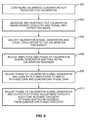
- FIG. 8shows the primary calibration steps 200 through 210 .
- FIG. 9shows the sub-steps of calibration step 200 of FIG. 8 .
- FIG. 10shows the sub-steps of calibration step 202 of FIG. 8 .
- FIG. 11shows the sub-steps of calibration step 204 of FIG. 8 .
- FIG. 12shows the sub-steps of calibration step 206 of FIG. 8 .
- FIG. 13shows the sub-steps of calibration step 208 of FIG. 8 .
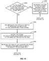
- FIGS. 14 and 15show the sub-steps of calibration step 210 of FIG. 8 .
- the present inventionis a quadrature VLIF receiver, including calibration circuitry, and methods to closely match signal processing of an in-phase signal path and a quadrature-phase signal path to optimize VLIF image rejection.
- the calibration circuitryincludes a variable gain variable-phase calibration signal generator, a variable gain amplifier for each signal path, phase adjustment circuitry for each signal path, and switching circuitry to support calibration steps.
- the calibration signal generatorsupplies a calibration signal at the same frequency as mixer local oscillator signals; therefore, during calibration, all signals downstream of the VLIF mixer are at DC, which simplifies calibration measurements.
- the calibration circuitryresponds quickly to calibration signals, thereby minimizing calibration times.
- a power up calibrationis performed at power up to perform an initial calibration; however, since calibration times have been minimized, an update calibration is performed on each channel just before a communications exchange on that channel.
- the calibration signal and the mixer local oscillator signalsare provided from a common frequency synthesizer. Therefore, synthesizer phase noise is cancelled out during calibration.
- the present inventionis designed for low power applications, including cell phone applications, and may be used in the personal communications services (PCS) band (1930 to 1990 Mhz), the digital cellular system (DCS) band (1805 to 1880 Mhz), the global system for mobile communications (GSM) band (869 to 894 Mhz), and the extended GSM (EGSM) band (925 to 960 Mhz).
- PCSpersonal communications services
- DCSdigital cellular system
- GSMglobal system for mobile communications
- EGSMextended GSM
- One embodiment of the present inventionis a calibrated quadrature VLIF receiver 24 as shown in FIG. 2 .
- An RF input signal RF INfeeds RF amplification, filtering, and switching circuitry 26 , which receives an RF calibration signal RF CAL from an RF frequency synthesizer and calibration signal generator 28 .
- the RF amplification, filtering, and switching circuitry 26may provide amplification, filtering, or both, for the RF signals RF IN , RF CAL , or both, and then select either RF IN or RF CAL to provide an RF output RF MIX feeding a calibrated quadrature VLIF mixer 30 .
- the calibrated quadrature VLIF mixer 30receives an in-phase local oscillator signal I RF and a quadrature-phase local oscillator signal Q RF from the RF frequency synthesizer and calibration signal generator 28 .
- the calibrated quadrature VLIF mixer 30includes an in-phase mixer, which multiplies RF MIX and I RF to create an in-phase VLIF signal I VLIF , and a quadrature-phase mixer, which multiplies RF MIX and Q RF to create a quadrature-phase VLIF signal Q VLIF .
- the RF frequency synthesizer and calibration signal generator 28uses an input reference clock REFCLK to generate RF CAL , I RF , and Q RF , which are all at the same frequency. I RF is phase-shifted from Q RF by essentially 90 degrees.
- I VLIF and Q VLIFare DC signals used for calibration.
- I VLIF and Q VLIFare VLIF signals.
- the present inventionrelies on a correlation between DC signals during calibration and VLIF signals during normal operation.
- the frequency of I VLIF and Q VLIFmay be essentially 175 Khz.
- Quadrature VLIF calibration circuitry 32receives I VLIF and Q VLIF , and may apply amplitude calibration adjustments, phase calibration adjustments, or both, to the VLIF signals I VLIF , Q VLIF , or both, to create a calibrated in-phase VLIF signal I CALVLIF and a calibrated quadrature-phase VLIF signal Q CALVLIF .
- I CALVLIF and Q CALVLIFfeed calibrated quadrature VLIF filtering, switching, and ND converter circuitry 34 , which may filter I CALVLIF , Q CALVLIF , or both, and then route either I CALVLIF or Q CALVLIF to ND conversion circuitry to convert analog VLIF quadrature signals into in-phase digital VLIF data I DIGITAL and quadrature-phase digital VLIF data Q DIGITAL .
- I DIGITAL and Q DIGITALare fed to other digital circuitry for calibration processing, de-modulation, and data extraction (not shown).
- the RF amplification, filtering, and switching circuitry 26is designed for a single communications band, as shown in FIG. 3 .
- An LNA 36receives RF IN and feeds an RF bandpass filter 38 , which then feeds an RF mixer preamplifier 40 .
- a first RF switch 42receives the output from the RF mixer preamplifier 40 and also receives RF CAL , and then selects one of the two to provide a signal to a calibrated RF bandpass filter 44 , which then provides RF MIX .
- the first RF switch 42selects RF CAL .
- the first RF switch 42selects the output from the RF mixer preamplifier.
- the RF amplification, filtering, and switching circuitry 26is designed for four communications bands, as shown in FIG. 4 , which may include the PCS band, the DCS band, the GSM band, and the EGSM band.
- a PCS band LNA 46 and a DCS band LNA 48receive RF IN and feed a highband RF bandpass filter 50 , which then feeds a highband RF mixer preamplifier 52 .
- a second RF switch 54receives the output from the highband RF mixer preamplifier 52 and feeds a calibrated highband RF bandpass filter 56 .
- An EGSM band LNA 58 and a GSM band LNA 60receive RF IN and feed a lowband RF bandpass filter 62 , which then feeds a lowband RF mixer preamplifier 64 .
- a third RF switch 66receives the output from the lowband RF mixer preamplifier 64 and feeds a calibrated lowband RF bandpass filter 68 .
- the calibrated highband RF bandpass filter 56 and the calibrated lowband RF bandpass filter 68feed a fourth RF switch 70 , which provides RF MIX .
- a fifth RF switch 72receives RF CAL and feeds both the second RF switch 54 and the third RF switch 66 .
- the second RF switch 54selects input signals from either the highband RF mixer preamplifier 52 or the fifth RF switch 72 for either calibration or normal operation.
- the third RF switch 66selects input signals from either the lowband RF mixer preamplifier 64 or the fifth RF switch 72 for either calibration or normal operation.
- the fourth RF switch 70selects input signals from one of the RF bandpass filters 56 , 68 for either highband or lowband signals during both calibration and normal operations.
- a frequency multiplier 74receives REFCLK, which is then multiplied to generate an RF reference clock RF REF .
- RF phase adjustment circuitry 76receives RF REF and applies an adjustable phase-shift to create a phase-adjusted calibration signal, which then feeds a variable gain RF amplifier 78 .
- the variable gain RF amplifier 78applies an adjustable gain to create RF CAL .
- An in-phase RF mixer amplifier 80receives RF REF and then provides buffering to create I RF .
- a 90-degree phase shifter 82receives RF REF and applies a 90-degree phase-shift to create a 90-degree shifted local oscillator signal, which then feeds a quadrature-phase RF mixer amplifier 84 .
- the quadrature-phase RF mixer amplifier 84applies buffering to create Q RF .
- An in-phase variable gain VLIF amplifier 86receives I VLIF and applies an adjustable gain to create a gain-calibrated in-phase VLIF signal I GVLIF , which then feeds an in-phase VLIF summing circuit 88 and a quadrature-phase phase adjustment circuit 90 .
- a quadrature-phase variable gain VLIF amplifier 92receives Q VLIF and applies an adjustable gain to create a gain-calibrated quadrature-phase VLIF signal Q GVLIF , which then feeds a quadrature-phase VLIF summing circuit 94 and an in-phase phase adjustment circuit 96 .
- the quadrature-phase phase adjustment circuit 90provides a phase adjustment to Q GVLIF by taking some in-phase signal, specifically I GVLIF , to generate a quadrature-phase error signal Q ERROR , which is then fed into the quadrature-phase VLIF summing circuit 94 .
- the quadrature-phase VLIF summing circuit 94phase calibrates the gain-calibrated quadrature-phase VLIF signal Q GVLIF by adding Q GVLIF to Q ERROR to create the calibrated quadrature-phase VLIF signal Q CALVLIF .
- the in-phase phase adjustment circuit 96provides a phase adjustment to I GVLIF , by taking some quadrature-phase signal, specifically Q GVLIF , to generate an in-phase error signal I ERROR , which is then fed into the in-phase VLIF summing circuit 88 .
- the in-phase VLIF summing circuit 88phase calibrates the gain-calibrated in-phase VLIF signal I GVLIF by adding I GVLIF to I ERROR to create the calibrated in-phase VLIF signal I CALVLIF .
- a VLIF bandpass filter 98receives I CALVLIF and Q CALVLIF .
- VLIF bandpass filter passive elements 100are connected to I CALVLIF through a first VLIF switch 102 and to Q CALVLIF through a second VLIF switch 104 .
- the first and second VLIF switches 102 , 104are used to disconnect the VLIF bandpass filter passive elements 100 during calibration to minimize calibration times.
- An input to a first VLIF calibration amplifier 106is connected to a third VLIF switch 108 , which is connected to and used to select either I CALVLIF or Q CALVLIF during calibration.
- An amplifier gain switch 110is used to select either a high gain or low gain setting for the first VLIF calibration amplifier 106 .
- An input to a second VLIF calibration amplifier 112is connected to a fourth VLIF switch 114 through a fifth VLIF switch 116 .
- the fourth VLIF switch 114is connected to and used to select either an inverting output or a non-inverting output from the first VLIF calibration amplifier 106 for peak-to-peak measurements.
- the fifth VLIF switch 116is used to either ground the input to the second VLIF calibration amplifier 112 or to connect the input to an output from the first VLIF calibration amplifier 106 . Peak-to-peak measurements may be made to minimize errors due to offsets, low frequency 1/f noise, and intermodulation effects.
- I DIGITALis provided from an output of an in-phase ND converter 118 , which may have a resolution of + or ⁇ 12 bits.
- An input of the in-phase ND converter 118is connected to a sixth VLIF switch 120 , which is connected to and selects either an in-phase output from the VLIF bandpass filter 98 or an output from the second VLIF calibration amplifier 112 .
- Q DIGITALis provided from an output of a quadrature-phase A/D converter 122 , which may have a resolution of + or ⁇ 12 bits.
- An input of the quadrature-phase A/D converter 122is connected to a seventh VLIF switch 124 , which is connected to and selects either a quadrature-phase output from the VLIF bandpass filter 98 or the output from the second VLIF calibration amplifier 112 . All of the settings of the third, fourth, fifth, sixth, and seventh VLIF switches 108 , 114 , 116 , 120 , 124 and the amplifier gain switch 110 are used during calibration.
- a calibrationis performed after power-up of the calibrated quadrature VLIF receiver 24 , called power-up calibration, and prior to packet reception on a specific receiver channel, called update calibration.
- a power-up calibrationis performed for each received band with the RF frequency synthesizer and calibration signal generator 28 adjusted to each band's center frequency.
- Each update calibrationis performed with the RF frequency synthesizer and calibration signal generator 28 adjusted to the frequency of the specific receiver channel.
- Power-up calibrationscompensate for initial manufacturing and process tolerances.
- Update calibrationscompensate for variations due to temperature, power supply, and specific channel frequency.
- rejection of image frequenciesmay be at least 50 db
- power-up calibrationsmay take less than 1 millisecond (mS) per frequency band
- update calibrationsmay take less than 90 microseconds (uS).
- the primary calibration processis shown for the second embodiment of the present invention in FIG. 8 .
- the calibrated quadrature VLIF receiver 24is configured for calibration (step 200 ).
- the calibration signal generatoris adjusted for an output of essentially zero volts. Offset voltages of calibration measurement circuitry and signal path circuitry are measured and then subtracted-out in all subsequent calibration steps (step 202 ). Step 202 may be omitted for update calibrations.
- the calibration signal generator and local oscillatorsare adjusted such that the frequencies of RF CAL , I RF , and Q RF are all at a single appropriate calibration frequency (step 204 ). Step 204 may be performed during step 200 for update calibrations to minimize calibration times.
- the calibration signal generatoris adjusted to establish initial calibration settings for RF CAL and to take initial calibration measurements (step 206 ).
- the calibration signal generatoris adjusted to provide appropriate phase settings for RF CAL , then the gain of the in-phase variable gain VLIF amplifier 86 , the gain of the quadrature-phase variable gain VLIF amplifier 92 , or both, is adjusted to match the amplitudes of in-phase VLIF circuitry with quadrature-phase VLIF circuitry (step 208 ).
- the calibration signal generatoris adjusted to provide appropriate phase settings for RF CAL , then the output of the in-phase phase adjustment circuit 96 , the output of the quadrature-phase phase adjustment circuit 90 , or both, is adjusted such that I CALVLIF is phase-shifted essentially 90 degrees from Q CALVLIF (step 210 ).
- each calibration stepThe sub-steps of each calibration step are provided below. Each sub-step applies to both power-up and update calibrations except where noted. Sub-steps correlating to steps 204 through 210 may be repeated for each RF band to be calibrated for power-up calibrations.
- step 200for the second embodiment of the present invention are shown in FIG. 9 .
- upstream RF circuitryincludes a transmit/receive switch (not shown), select the transmit position (step 200 A). This minimizes interference from other RF circuitry. Wait for circuit temperatures to stabilize (step 200 B). Step 200 B may be omitted for update calibrations.
- Power down all RF LNAs 46 , 48 , 58 , 60 and all RF mixer preamplifiers 52 , 64 to minimize power consumption during calibrationstep 200 C).
- Adjust the frequency multiplier 74 such that the frequency of RF REF is at a nominal operating frequency for power-up calibrations or at the receive channel frequency for update calibrations(step 200 E).
- Adjust the RF phase adjustment circuitry 76 such that the phase of RF CAL is essentially equal to the phase of I RF(step 200 F).
- Adjust the output of the variable gain RF amplifier 78 such that RF CAL is essentially zero volts(step 200 G).
- Step 200 MSet the fourth VLIF switch 114 to select the non-inverting output from the first VLIF calibration amplifier 106 (step 200 M).
- Step 200 Nis omitted for update calibrations.
- the output of the second VLIF calibration amplifier 112will be its amplified offset voltage.
- step 202 for power-up calibrations for the second embodiment of the present inventionare shown in FIG. 10 .
- step 202 CSubtract out the value of Q DIGITAL measured in step 202 C from all subsequent readings of Q DIGITAL whenever the sixth and seventh VLIF switches 120 , 124 are configured to route the output of the second VLIF calibration amplifier 112 to the quadrature-phase ND converter 122 (step 202 D).
- VLIF switches 120 , 124Configure the sixth and seventh VLIF switches 120 , 124 to route the in-phase output from the VLIF bandpass filter 98 to the in-phase A/D converter 118 and the quadrature-phase output from the VLIF bandpass filter 98 to the quadrature-phase ND converter 122 in preparation to measure the signal path offset voltages (step 202 E). Measure the offset voltage from the in-phase signal path by reading the value of I DIGITAL (step 202 F). Subtract out the value of I DIGITAL measured in step 202 F from all subsequent readings of I DIGITAL whenever the sixth VLIF switch 120 is configured to route the in-phase output from the VLIF bandpass filter 98 to the in-phase A/D converter 118 (step 202 G).
- step 202 HMeasure the offset voltage from the quadrature-phase signal path by reading the value of Q DIGITAL (step 202 H). Subtract out the value of Q DIGITAL measured in step 202 H from all subsequent readings of Q DIGITAL whenever the seventh VLIF switch 124 is configured to route the quadrature-phase output from the VLIF bandpass filter 98 to the quadrature-phase ND converter 122 (step 202 I).
- Other embodiments of the present inventionmay use a VLIF bandpass filter 98 with circuitry to null-out in-phase and quadrature-phase offset voltages. Such embodiments would replace steps 202 F through 2021 with other steps to adjust out the offset voltages.
- step 204 AAdjusts the frequency multiplier 74 such that the frequency of RF REF is at the center of the band being calibrated (step 204 A).
- Step 204 Amay be omitted for update calibrations. Since the frequency multiplier 74 feeds the circuitry that provides RF CAL , I RF , and Q RF , all three signals will be at the same operating frequency. Wait until the frequency multiplier 74 has stabilized, which may be within 0.01% of its final value (step 204 B).
- step 206For the second embodiment of the present invention are shown in FIG. 12 .
- Adjust the output of the variable gain RF amplifier 78such that the amplitude of RF CAL is a nominal value for power-up calibrations and to the last calibration value for update calibrations (step 206 C).
- Adjust the RF phase adjustment circuitry 76such that the value of (I DIGITAL +Q DIGITAL )/2 is maximized, which maximizes Q CALVLIF (step 206 D). Adjust the output of the variable gain RF amplifier 78 such that the value of (I DIGITAL +Q DIGITAL )/2 is equal to 75% of the full-scale value of the ND converters 118 , 122 (step 206 E). Reconfigure the third VLIF switch 108 to route I CALVLIF to the input of the first VLIF calibration amplifier 106 (step 206 F) in preparation for calibration measurements. Adjust the RF phase adjustment circuitry 76 such that the value of (I DIGITAL +Q DIGITAL )/2 is maximized, which maximizes I CALVLIF (step 206 G).
- step 208for the second embodiment of the present invention are shown in FIG. 13 . If the value of (I DIGITAL +Q DIGITAL )/2 in step 206 G, which is the maximum value of amplitude of I CALVLIF , is less than the value of (I DIGITAL +Q DIGITAL )/2 in step 206 E, which is the maximum value of amplitude of Q CALVLIF , then the gain of the in-phase path is less than the gain of the quadrature-phase path; therefore proceed to step 208 B, otherwise proceed to step 208 C (step 208 A).
- Step 208 Bproceeds as follows. Increase the gain of the in-phase variable gain VLIF amplifier 86 until the value of (I DIGITAL +Q DIGITAL )/2 matches the value of (I DIGITAL +Q DIGITAL )/2 in step 206 E, which matches the gains of the in-phase path and the quadrature-phase path, then proceed to step 210 H ( FIG. 15 ).
- Step 208 Cproceeds as follows.
- the maximum value of amplitude of Q CALVLIFis less than the maximum value of amplitude of I CALVLIF ; therefore, reconfigure the third VLIF switch 108 to route Q CALVLIF to the input of the first VLIF calibration amplifier 106 to prepare for calibration measurements (step 208 C).
- Adjust the RF phase adjustment circuitry 76 to the same phase setting as in step 206 D(step 208 D).
- step 210for the second embodiment of the present invention are shown in FIGS. 14 and 15 .
- Reconfigure the third VLIF switch 108 to route I CALVLIF to the input of the first VLIF calibration amplifier 106 in preparation to measure the amplitude of the in-phase signalstep 210 A.
- Adjust the RF phase adjustment circuitry 76 such that RF CAL is phase-shifted from I RF and Q RF by essentially 45 degreesstep 210 B.
- step 210 CSet the amplifier gain switch 110 of the first VLIF calibration amplifier 106 to the high gain position.
- step 210 DAdjust the output of the in-phase phase adjustment circuit 96 until the value of (I DIGITAL +Q DIGITAL )/2 is equal to the Cosine of 45 degrees times the value of (I DIGITAL +Q DIGITAL )/2 in step 208 E (step 210 D).
- Reconfigure the third VLIF switch 108 to route Q CALVLIF to the input of the first VLIF calibration amplifier 106 in preparation to measure the amplitude of the quadrature-phase signalstep 210 E.
- step 210 HAdjust the RF phase adjustment circuitry 76 such that RF CAL is phase-shifted from I RF and Q RF by essentially 45 degrees.
- step 210 KReconfigure the third VLIF switch 108 to route Q CALVLIF to the input of the first VLIF calibration amplifier 106 in preparation to measure the amplitude of the quadrature-phase signal. Adjust the output of the quadrature-phase phase adjustment circuit 90 until the value of (I DIGITAL +Q DIGITAL )/2 is equal to the value of (I DIGITAL +Q DIGITAL )/2 in step 210 J (step 210 L). This completes the phase adjustment portion of the calibration.
- Some embodiments of the present inventionmay use mixer nonlinearity correction factors during calibration. Some embodiments of the present invention may take peak-to-peak measurements during calibration to maximize the resolution of ND converter readings. In the second embodiment of the present invention, peak-to-peak measurements are performed by reading values of I DIGITAL and Q DIGITAL with the non-inverting output of the first VLIF calibration amplifier 106 routed to the input of the second VLIF calibration amplifier 112 , followed by reading values of I DIGITAL and Q DIGITAL with the inverting output of the first VLIF calibration amplifier 106 routed to the input of the second VLIF calibration amplifier 112 , and then subtracting the two readings. Some embodiments of the present invention may use VLIF calibration amplifiers with two or more gain settings. Such embodiments may include calibration steps to calibrate the gain settings. Certain embodiments of the present invention may add look-up tables to compensate for minor phase errors in the RF calibration signal RF CAL , particularly at the Cos 45 point.
Landscapes
- Engineering & Computer Science (AREA)
- Computer Networks & Wireless Communication (AREA)
- Signal Processing (AREA)
- Power Engineering (AREA)
- Digital Transmission Methods That Use Modulated Carrier Waves (AREA)
- Superheterodyne Receivers (AREA)
Abstract
Description
Claims (7)
Priority Applications (1)
| Application Number | Priority Date | Filing Date | Title |
|---|---|---|---|
| US11/534,072US7773965B1 (en) | 2006-09-21 | 2006-09-21 | Calibrated quadrature very low intermediate frequency receiver |
Applications Claiming Priority (1)
| Application Number | Priority Date | Filing Date | Title |
|---|---|---|---|
| US11/534,072US7773965B1 (en) | 2006-09-21 | 2006-09-21 | Calibrated quadrature very low intermediate frequency receiver |
Publications (1)
| Publication Number | Publication Date |
|---|---|
| US7773965B1true US7773965B1 (en) | 2010-08-10 |
Family
ID=42537771
Family Applications (1)
| Application Number | Title | Priority Date | Filing Date |
|---|---|---|---|
| US11/534,072Active2029-05-10US7773965B1 (en) | 2006-09-21 | 2006-09-21 | Calibrated quadrature very low intermediate frequency receiver |
Country Status (1)
| Country | Link |
|---|---|
| US (1) | US7773965B1 (en) |
Cited By (42)
| Publication number | Priority date | Publication date | Assignee | Title |
|---|---|---|---|---|
| US20060094391A1 (en)* | 2004-10-29 | 2006-05-04 | Hooman Darabi | Method and system for an analog zero-IF interface for GSM receivers |
| US20090081961A1 (en)* | 2007-09-24 | 2009-03-26 | Ahmadreza Rofougaran | Method and system for injection locking an oscillator via frequency multiplication of a multiphase signal |
| US20100156690A1 (en)* | 2008-12-22 | 2010-06-24 | Electronics And Telecommunications Research Institute | Digital direct conversion receiving apparatus and method |
| US20100167674A1 (en)* | 2007-05-31 | 2010-07-01 | Freescale Semiconductor, Inc. | Integrated circuit, wireless communication unit and method for determining quadrature imbalance |
| US20100173601A1 (en)* | 2007-01-22 | 2010-07-08 | Freescale Semiconductor, Inc. | Very low intermediate frequency (vlif) receiver |
| US20120098592A1 (en)* | 2010-10-22 | 2012-04-26 | Global Unichip Corp. | Filter auto-calibration using multi-clock generator |
| WO2014125325A1 (en)* | 2013-02-12 | 2014-08-21 | Freescale Semiconductor, Inc. | Active iq and quadrature generator for high frequency applications |
| US20150288394A1 (en)* | 2014-04-03 | 2015-10-08 | Rafael Microelectronics, Inc. | Multi-user satellite receiving system and method thereof |
| US9207692B2 (en) | 2012-10-18 | 2015-12-08 | Rf Micro Devices, Inc. | Transitioning from envelope tracking to average power tracking |
| US9225231B2 (en) | 2012-09-14 | 2015-12-29 | Rf Micro Devices, Inc. | Open loop ripple cancellation circuit in a DC-DC converter |
| US20160020859A1 (en)* | 2012-11-13 | 2016-01-21 | Stephane Laurent-Michel | Method for calibrating distortion cancelation in duplex communication systems |
| US9246460B2 (en) | 2011-05-05 | 2016-01-26 | Rf Micro Devices, Inc. | Power management architecture for modulated and constant supply operation |
| US9247496B2 (en) | 2011-05-05 | 2016-01-26 | Rf Micro Devices, Inc. | Power loop control based envelope tracking |
| US9250643B2 (en) | 2011-11-30 | 2016-02-02 | Rf Micro Devices, Inc. | Using a switching signal delay to reduce noise from a switching power supply |
| US9256234B2 (en) | 2011-12-01 | 2016-02-09 | Rf Micro Devices, Inc. | Voltage offset loop for a switching controller |
| US9263996B2 (en) | 2011-07-20 | 2016-02-16 | Rf Micro Devices, Inc. | Quasi iso-gain supply voltage function for envelope tracking systems |
| US20160049921A1 (en)* | 2014-08-12 | 2016-02-18 | Rf Micro Devices, Inc. | Configurable rf transmit/receive multiplexer |
| US9280163B2 (en) | 2011-12-01 | 2016-03-08 | Rf Micro Devices, Inc. | Average power tracking controller |
| US9294041B2 (en) | 2011-10-26 | 2016-03-22 | Rf Micro Devices, Inc. | Average frequency control of switcher for envelope tracking |
| US9300252B2 (en) | 2013-01-24 | 2016-03-29 | Rf Micro Devices, Inc. | Communications based adjustments of a parallel amplifier power supply |
| US9298198B2 (en) | 2011-12-28 | 2016-03-29 | Rf Micro Devices, Inc. | Noise reduction for envelope tracking |
| US9374005B2 (en) | 2013-08-13 | 2016-06-21 | Rf Micro Devices, Inc. | Expanded range DC-DC converter |
| US9377797B2 (en) | 2011-12-01 | 2016-06-28 | Rf Micro Devices, Inc. | Multiple mode RF power converter |
| US9379667B2 (en) | 2011-05-05 | 2016-06-28 | Rf Micro Devices, Inc. | Multiple power supply input parallel amplifier based envelope tracking |
| US9401678B2 (en) | 2010-04-19 | 2016-07-26 | Rf Micro Devices, Inc. | Output impedance compensation of a pseudo-envelope follower power management system |
| US9431974B2 (en) | 2010-04-19 | 2016-08-30 | Qorvo Us, Inc. | Pseudo-envelope following feedback delay compensation |
| US9479118B2 (en) | 2013-04-16 | 2016-10-25 | Rf Micro Devices, Inc. | Dual instantaneous envelope tracking |
| US9484797B2 (en) | 2011-10-26 | 2016-11-01 | Qorvo Us, Inc. | RF switching converter with ripple correction |
| US9494962B2 (en) | 2011-12-02 | 2016-11-15 | Rf Micro Devices, Inc. | Phase reconfigurable switching power supply |
| US9515621B2 (en) | 2011-11-30 | 2016-12-06 | Qorvo Us, Inc. | Multimode RF amplifier system |
| US9614476B2 (en) | 2014-07-01 | 2017-04-04 | Qorvo Us, Inc. | Group delay calibration of RF envelope tracking |
| US9621113B2 (en) | 2010-04-19 | 2017-04-11 | Qorvo Us, Inc. | Pseudo-envelope following power management system |
| US9627975B2 (en) | 2012-11-16 | 2017-04-18 | Qorvo Us, Inc. | Modulated power supply system and method with automatic transition between buck and boost modes |
| US9813036B2 (en) | 2011-12-16 | 2017-11-07 | Qorvo Us, Inc. | Dynamic loadline power amplifier with baseband linearization |
| US9843342B2 (en) | 2014-08-12 | 2017-12-12 | Qorvo Us, Inc. | Tunable RF transmit/receive multiplexer |
| US9843294B2 (en) | 2015-07-01 | 2017-12-12 | Qorvo Us, Inc. | Dual-mode envelope tracking power converter circuitry |
| US9912297B2 (en) | 2015-07-01 | 2018-03-06 | Qorvo Us, Inc. | Envelope tracking power converter circuitry |
| US9954436B2 (en) | 2010-09-29 | 2018-04-24 | Qorvo Us, Inc. | Single μC-buckboost converter with multiple regulated supply outputs |
| US9973147B2 (en) | 2016-05-10 | 2018-05-15 | Qorvo Us, Inc. | Envelope tracking power management circuit |
| US10312960B2 (en) | 2014-08-12 | 2019-06-04 | Qorvo Us, Inc. | Switchable RF transmit/receive multiplexer |
| US10476437B2 (en) | 2018-03-15 | 2019-11-12 | Qorvo Us, Inc. | Multimode voltage tracker circuit |
| EP4246816A1 (en)* | 2022-03-18 | 2023-09-20 | Imec VZW | Phased array transceiver element |
Citations (6)
| Publication number | Priority date | Publication date | Assignee | Title |
|---|---|---|---|---|
| US20030165203A1 (en)* | 2001-08-10 | 2003-09-04 | Rishi Mohindra | Quadrature gain and phase imbalance correction in a receiver |
| US20040152436A1 (en)* | 2003-01-31 | 2004-08-05 | Ditrans Corporation | Systems and methods for coherent adaptive calibration in a receiver |
| US20050221781A1 (en)* | 2004-04-02 | 2005-10-06 | Lin Hung C | DC offset and 1/f noise compensation of a direct conversion receiver |
| US20060035617A1 (en)* | 2004-08-13 | 2006-02-16 | Jae-Wan Kim | Intermediate frequency receiver with improved image rejection ratio |
| US20070099570A1 (en)* | 2005-10-31 | 2007-05-03 | Silicon Laboratories, Inc. | Receiver with multi-tone wideband I/Q mismatch calibration and method therefor |
| US7362826B2 (en)* | 2003-09-29 | 2008-04-22 | Silicon Laboratories, Inc. | Receiver including an oscillation circuit for generating an image rejection calibration tone |
- 2006
- 2006-09-21USUS11/534,072patent/US7773965B1/enactiveActive
Patent Citations (6)
| Publication number | Priority date | Publication date | Assignee | Title |
|---|---|---|---|---|
| US20030165203A1 (en)* | 2001-08-10 | 2003-09-04 | Rishi Mohindra | Quadrature gain and phase imbalance correction in a receiver |
| US20040152436A1 (en)* | 2003-01-31 | 2004-08-05 | Ditrans Corporation | Systems and methods for coherent adaptive calibration in a receiver |
| US7362826B2 (en)* | 2003-09-29 | 2008-04-22 | Silicon Laboratories, Inc. | Receiver including an oscillation circuit for generating an image rejection calibration tone |
| US20050221781A1 (en)* | 2004-04-02 | 2005-10-06 | Lin Hung C | DC offset and 1/f noise compensation of a direct conversion receiver |
| US20060035617A1 (en)* | 2004-08-13 | 2006-02-16 | Jae-Wan Kim | Intermediate frequency receiver with improved image rejection ratio |
| US20070099570A1 (en)* | 2005-10-31 | 2007-05-03 | Silicon Laboratories, Inc. | Receiver with multi-tone wideband I/Q mismatch calibration and method therefor |
Non-Patent Citations (1)
| Title |
|---|
| Terrovitis et al., "Intermodulation Distortion in Current-Commutating CMOS Mixers," IEEE Journal of Solid-State Circuits, Oct. 2000, pp. 1461-1473, vol. 35, No. 10, IEEE. |
Cited By (56)
| Publication number | Priority date | Publication date | Assignee | Title |
|---|---|---|---|---|
| US7965994B2 (en)* | 2004-10-29 | 2011-06-21 | Broadcom Corporation | Method and system for an analog zero-IF interface for GSM receivers |
| US20060094391A1 (en)* | 2004-10-29 | 2006-05-04 | Hooman Darabi | Method and system for an analog zero-IF interface for GSM receivers |
| US20100173601A1 (en)* | 2007-01-22 | 2010-07-08 | Freescale Semiconductor, Inc. | Very low intermediate frequency (vlif) receiver |
| US8693968B2 (en)* | 2007-01-22 | 2014-04-08 | Freescale Semiconductor, Inc. | Very low intermediate frequency (VLIF) receiver |
| US8942655B2 (en)* | 2007-05-31 | 2015-01-27 | Freescale Semiconductor, Inc. | Integrated circuit, wireless communication unit and method for determining quadrature imbalance |
| US20100167674A1 (en)* | 2007-05-31 | 2010-07-01 | Freescale Semiconductor, Inc. | Integrated circuit, wireless communication unit and method for determining quadrature imbalance |
| US20090081961A1 (en)* | 2007-09-24 | 2009-03-26 | Ahmadreza Rofougaran | Method and system for injection locking an oscillator via frequency multiplication of a multiphase signal |
| US20100156690A1 (en)* | 2008-12-22 | 2010-06-24 | Electronics And Telecommunications Research Institute | Digital direct conversion receiving apparatus and method |
| US8102293B2 (en)* | 2008-12-22 | 2012-01-24 | Electronics And Telecommunications Research Institute | Digital direct conversion receiving apparatus and method |
| US9621113B2 (en) | 2010-04-19 | 2017-04-11 | Qorvo Us, Inc. | Pseudo-envelope following power management system |
| US9401678B2 (en) | 2010-04-19 | 2016-07-26 | Rf Micro Devices, Inc. | Output impedance compensation of a pseudo-envelope follower power management system |
| US9431974B2 (en) | 2010-04-19 | 2016-08-30 | Qorvo Us, Inc. | Pseudo-envelope following feedback delay compensation |
| US9954436B2 (en) | 2010-09-29 | 2018-04-24 | Qorvo Us, Inc. | Single μC-buckboost converter with multiple regulated supply outputs |
| US8768994B2 (en)* | 2010-10-22 | 2014-07-01 | Taiwan Semiconductor Manufacturing Company, Ltd. | Filter auto-calibration using multi-clock generator |
| US20120098592A1 (en)* | 2010-10-22 | 2012-04-26 | Global Unichip Corp. | Filter auto-calibration using multi-clock generator |
| US9385688B2 (en) | 2010-10-22 | 2016-07-05 | Taiwan Semiconductor Manufacturing Company, Ltd. | Filter auto-calibration using multi-clock generator |
| US9246460B2 (en) | 2011-05-05 | 2016-01-26 | Rf Micro Devices, Inc. | Power management architecture for modulated and constant supply operation |
| US9247496B2 (en) | 2011-05-05 | 2016-01-26 | Rf Micro Devices, Inc. | Power loop control based envelope tracking |
| US9379667B2 (en) | 2011-05-05 | 2016-06-28 | Rf Micro Devices, Inc. | Multiple power supply input parallel amplifier based envelope tracking |
| US9263996B2 (en) | 2011-07-20 | 2016-02-16 | Rf Micro Devices, Inc. | Quasi iso-gain supply voltage function for envelope tracking systems |
| US9294041B2 (en) | 2011-10-26 | 2016-03-22 | Rf Micro Devices, Inc. | Average frequency control of switcher for envelope tracking |
| US9484797B2 (en) | 2011-10-26 | 2016-11-01 | Qorvo Us, Inc. | RF switching converter with ripple correction |
| US9515621B2 (en) | 2011-11-30 | 2016-12-06 | Qorvo Us, Inc. | Multimode RF amplifier system |
| US9250643B2 (en) | 2011-11-30 | 2016-02-02 | Rf Micro Devices, Inc. | Using a switching signal delay to reduce noise from a switching power supply |
| US9280163B2 (en) | 2011-12-01 | 2016-03-08 | Rf Micro Devices, Inc. | Average power tracking controller |
| US9256234B2 (en) | 2011-12-01 | 2016-02-09 | Rf Micro Devices, Inc. | Voltage offset loop for a switching controller |
| US9377797B2 (en) | 2011-12-01 | 2016-06-28 | Rf Micro Devices, Inc. | Multiple mode RF power converter |
| US9494962B2 (en) | 2011-12-02 | 2016-11-15 | Rf Micro Devices, Inc. | Phase reconfigurable switching power supply |
| US9813036B2 (en) | 2011-12-16 | 2017-11-07 | Qorvo Us, Inc. | Dynamic loadline power amplifier with baseband linearization |
| US9298198B2 (en) | 2011-12-28 | 2016-03-29 | Rf Micro Devices, Inc. | Noise reduction for envelope tracking |
| US9225231B2 (en) | 2012-09-14 | 2015-12-29 | Rf Micro Devices, Inc. | Open loop ripple cancellation circuit in a DC-DC converter |
| US9207692B2 (en) | 2012-10-18 | 2015-12-08 | Rf Micro Devices, Inc. | Transitioning from envelope tracking to average power tracking |
| US20160020859A1 (en)* | 2012-11-13 | 2016-01-21 | Stephane Laurent-Michel | Method for calibrating distortion cancelation in duplex communication systems |
| US9627975B2 (en) | 2012-11-16 | 2017-04-18 | Qorvo Us, Inc. | Modulated power supply system and method with automatic transition between buck and boost modes |
| US9929696B2 (en) | 2013-01-24 | 2018-03-27 | Qorvo Us, Inc. | Communications based adjustments of an offset capacitive voltage |
| US9300252B2 (en) | 2013-01-24 | 2016-03-29 | Rf Micro Devices, Inc. | Communications based adjustments of a parallel amplifier power supply |
| US9897686B2 (en) | 2013-02-12 | 2018-02-20 | Nxp Usa, Inc. | Active IQ and quadrature generator for high frequency applications |
| WO2014125325A1 (en)* | 2013-02-12 | 2014-08-21 | Freescale Semiconductor, Inc. | Active iq and quadrature generator for high frequency applications |
| US9479118B2 (en) | 2013-04-16 | 2016-10-25 | Rf Micro Devices, Inc. | Dual instantaneous envelope tracking |
| US9374005B2 (en) | 2013-08-13 | 2016-06-21 | Rf Micro Devices, Inc. | Expanded range DC-DC converter |
| US20150288394A1 (en)* | 2014-04-03 | 2015-10-08 | Rafael Microelectronics, Inc. | Multi-user satellite receiving system and method thereof |
| US9548779B2 (en)* | 2014-04-03 | 2017-01-17 | Rafael Microelectronics, Inc. | Multi-user satellite receiving system and method thereof |
| US9614476B2 (en) | 2014-07-01 | 2017-04-04 | Qorvo Us, Inc. | Group delay calibration of RF envelope tracking |
| US9843342B2 (en) | 2014-08-12 | 2017-12-12 | Qorvo Us, Inc. | Tunable RF transmit/receive multiplexer |
| US12107619B2 (en) | 2014-08-12 | 2024-10-01 | Qorvo Us, Inc. | Switchable RF transmit/receive multiplexer |
| US9780866B2 (en)* | 2014-08-12 | 2017-10-03 | Qorvo Us, Inc. | Configurable RF transmit/receive multiplexer |
| US10312960B2 (en) | 2014-08-12 | 2019-06-04 | Qorvo Us, Inc. | Switchable RF transmit/receive multiplexer |
| US20160049921A1 (en)* | 2014-08-12 | 2016-02-18 | Rf Micro Devices, Inc. | Configurable rf transmit/receive multiplexer |
| US9941844B2 (en) | 2015-07-01 | 2018-04-10 | Qorvo Us, Inc. | Dual-mode envelope tracking power converter circuitry |
| US9948240B2 (en) | 2015-07-01 | 2018-04-17 | Qorvo Us, Inc. | Dual-output asynchronous power converter circuitry |
| US9912297B2 (en) | 2015-07-01 | 2018-03-06 | Qorvo Us, Inc. | Envelope tracking power converter circuitry |
| US9843294B2 (en) | 2015-07-01 | 2017-12-12 | Qorvo Us, Inc. | Dual-mode envelope tracking power converter circuitry |
| US9973147B2 (en) | 2016-05-10 | 2018-05-15 | Qorvo Us, Inc. | Envelope tracking power management circuit |
| US10476437B2 (en) | 2018-03-15 | 2019-11-12 | Qorvo Us, Inc. | Multimode voltage tracker circuit |
| EP4246816A1 (en)* | 2022-03-18 | 2023-09-20 | Imec VZW | Phased array transceiver element |
| US12255408B2 (en) | 2022-03-18 | 2025-03-18 | Imec Vzw | Phased array transceiver element |
Similar Documents
| Publication | Publication Date | Title |
|---|---|---|
| US7773965B1 (en) | Calibrated quadrature very low intermediate frequency receiver | |
| US7362826B2 (en) | Receiver including an oscillation circuit for generating an image rejection calibration tone | |
| US20090131006A1 (en) | Apparatus, integrated circuit, and method of compensating iq phase mismatch | |
| US7136431B2 (en) | DC offset correcting in a direct conversion or very low IF receiver | |
| KR101442265B1 (en) | Variable gain frequency multiplier, method for controlling the frequency and gain of a transmit signal using the same, and portable transceiver having a variable gain frequency multiplier | |
| US7224722B2 (en) | Direct conversion RF transceiver with automatic frequency control | |
| US7346325B2 (en) | Receiver, receiving method and portable wireless apparatus | |
| US7196579B2 (en) | Gain-controlled amplifier, receiver circuit and radio communication device | |
| KR101387262B1 (en) | System and method for generating local oscillator (lo) signals for a quadrature mixer | |
| US20040038649A1 (en) | Zero intermediate frequency to low intermediate frequency receiver architecture | |
| US20080113628A1 (en) | Methods and apparatus to provide an auxiliary receive path to support transmitter functions | |
| US20050075088A1 (en) | Wireless communication semiconductor integrated circuit device and wireless communication system | |
| US20040106380A1 (en) | Direct-conversion transceiver enabling digital calibration | |
| US20100248670A1 (en) | Direct conversion rf transceiver for wireless communication | |
| EP1330044B1 (en) | A direct conversion RF transceiver with automatic frequency control | |
| US6999744B2 (en) | Measurement of local oscillation leakage in a radio frequency integrated circuit | |
| EP1478097B1 (en) | Direct conversion receiver comprising DC offset reducing system and transmitter | |
| US20130128931A1 (en) | On-chip radio calibration | |
| US8159619B2 (en) | Multi-standard integrated television receiver | |
| US20060025099A1 (en) | Apparatus and method for downward mixing an input signal into an output signal | |
| CN116057843B (en) | Radio transceiver device and method | |
| US20170310520A1 (en) | Apparatus and methods for wideband receivers | |
| US7450925B2 (en) | Receiver for wireless communication systems and I/Q signal phase difference correction method therefor | |
| JP2010183347A (en) | Fm-am demodulator, radio receiver, electronic device, and image correction adjustment method | |
| WO2009130673A1 (en) | Calibration of communication apparatus |
Legal Events
| Date | Code | Title | Description |
|---|---|---|---|
| AS | Assignment | Owner name:RF MICRO DEVICES, INC., NORTH CAROLINA Free format text:ASSIGNMENT OF ASSIGNORS INTEREST;ASSIGNORS:VAN BRUNT, ROGER W.;MOFFAT, MARK ALEXANDER JOHN;PICKEN, STEVE;REEL/FRAME:018553/0148 Effective date:20061024 | |
| STCF | Information on status: patent grant | Free format text:PATENTED CASE | |
| AS | Assignment | Owner name:BANK OF AMERICA, N.A., AS ADMINISTRATIVE AGENT, TE Free format text:NOTICE OF GRANT OF SECURITY INTEREST IN PATENTS;ASSIGNOR:RF MICRO DEVICES, INC.;REEL/FRAME:030045/0831 Effective date:20130319 | |
| FPAY | Fee payment | Year of fee payment:4 | |
| AS | Assignment | Owner name:RF MICRO DEVICES, INC., NORTH CAROLINA Free format text:TERMINATION AND RELEASE OF SECURITY INTEREST IN PATENTS (RECORDED 3/19/13 AT REEL/FRAME 030045/0831);ASSIGNOR:BANK OF AMERICA, N.A., AS ADMINISTRATIVE AGENT;REEL/FRAME:035334/0363 Effective date:20150326 | |
| AS | Assignment | Owner name:QORVO US, INC., NORTH CAROLINA Free format text:MERGER;ASSIGNOR:RF MICRO DEVICES, INC.;REEL/FRAME:039196/0941 Effective date:20160330 | |
| FEPP | Fee payment procedure | Free format text:MAINTENANCE FEE REMINDER MAILED (ORIGINAL EVENT CODE: REM.) | |
| FEPP | Fee payment procedure | Free format text:7.5 YR SURCHARGE - LATE PMT W/IN 6 MO, LARGE ENTITY (ORIGINAL EVENT CODE: M1555) | |
| MAFP | Maintenance fee payment | Free format text:PAYMENT OF MAINTENANCE FEE, 8TH YEAR, LARGE ENTITY (ORIGINAL EVENT CODE: M1552) Year of fee payment:8 | |
| MAFP | Maintenance fee payment | Free format text:PAYMENT OF MAINTENANCE FEE, 12TH YEAR, LARGE ENTITY (ORIGINAL EVENT CODE: M1553); ENTITY STATUS OF PATENT OWNER: LARGE ENTITY Year of fee payment:12 |