US7773695B2 - Amplitude modulator - Google Patents
Amplitude modulatorDownload PDFInfo
- Publication number
- US7773695B2 US7773695B2US11/207,348US20734805AUS7773695B2US 7773695 B2US7773695 B2US 7773695B2US 20734805 AUS20734805 AUS 20734805AUS 7773695 B2US7773695 B2US 7773695B2
- Authority
- US
- United States
- Prior art keywords
- carrier signal
- signal
- circuitry
- path
- phase
- Prior art date
- Legal status (The legal status is an assumption and is not a legal conclusion. Google has not performed a legal analysis and makes no representation as to the accuracy of the status listed.)
- Active, expires
Links
Images


Classifications
- H—ELECTRICITY
- H03—ELECTRONIC CIRCUITRY
- H03C—MODULATION
- H03C1/00—Amplitude modulation
- H03C1/50—Amplitude modulation by converting angle modulation to amplitude modulation
- H—ELECTRICITY
- H03—ELECTRONIC CIRCUITRY
- H03C—MODULATION
- H03C1/00—Amplitude modulation
- H03C1/02—Details
- H03C1/04—Means in or combined with modulating stage for reducing angle modulation
- H—ELECTRICITY
- H03—ELECTRONIC CIRCUITRY
- H03C—MODULATION
- H03C2200/00—Indexing scheme relating to details of modulators or modulation methods covered by H03C
- H03C2200/0037—Functional aspects of modulators
- H03C2200/0079—Measures to linearise modulation or reduce distortion of modulation characteristics
Definitions
- the present inventionrelates to Radio Frequency (RF) signal processing circuitry, and more particularly, this invention relates to an energy efficient amplitude modulator exhibiting low phase noise and low residual phase shift.
- RFRadio Frequency
- Radio Frequency (RF) carrier modulationby which information is transmitted must demand the smallest bandwidth possible due to the general shortage of available spectrum.
- both the amplitude and the phase (i.e., frequency) of the carriermust be precisely controlled during modulation.
- Amplifying the modulated carrier without excessive distortion in the transmitter output stageimposes significant linearity constraints on the output stage amplifier.
- the power efficiency of the transmitteris very important where the transmitting end of the wireless link is battery powered.
- the transmitter output stageis the largest power consumer; hence, improvements in this stage are the most important.
- Class A RF amplifiersprovide a distortion-free output, but require large amounts of power.
- Non-linear amplifiers, including class B and class C amplifiersprovide higher RF output power and better efficiency.
- One of the most efficient RF power amplifiersis the class C RF amplifier in which the output transistor conducts current only at the time when the collector-emitter voltage is at its lowest value. Unfortunately, these amplifiers are very nonlinear and introduce substantial amplitude distortion. Because of this distortion, class C amplifiers are used mainly in FM transmitters in which the amplitude or “envelope” of the RF carrier is constant, and hence, such distortion has no effect on the output spectrum occupancy.
- Radio Frequency Identificationuses amplitude modulated signals.
- an RFID system 100includes RFID tags 102 , a reader 104 , and an optional backend system, e.g., server 106 .
- Each tag 102includes an IC chip and an antenna.
- the IC chipincludes a digital decoder needed to execute the computer commands that the tag 102 receives from the tag reader 104 .
- the IC chipalso includes a power supply circuit to extract and regulate power from the RF reader; a detector to decode signals from the reader; a backscatter modulator, a transmitter to send data back to the reader; anti-collision protocol circuits; and at least enough memory to store its EPC code.
- Communicationbegins with a reader 104 sending out signals to find the tag 102 .
- the reader 104decodes the data programmed into the tag 102 and sent back in the tag reply.
- the informationcan then be passed to the optional server 106 for processing, storage, and/or propagation to another computing device.
- RFID systemsuse reflected or “backscattered” radio frequency (RF) waves to transmit information from the tag 102 to the reader 104 . Since passive (Class-1 and Class-2) tags get all of their power from the reader signal, the tags are only powered when in the beam of the reader 104 . Class-3 and higher tags often include an on-board power source, e.g., a battery.
- RFradio frequency
- class A amplifiersare typically used.
- RFIDbecomes prominent as the tracking and identification system of choice, new RFID applications will be required.
- portable tag readerAs with any portable device, second only to reliability in importance is power consumption.
- the distortion inherent in non-linear amplifiershas been a barrier to use of class B and class C amplifiers in portable RFID transmitters.
- a circuit for amplitude modulating a carrier signalincludes a carrier signal input, circuitry for splitting the carrier signal into first and second paths, circuitry for phase modulating the carrier signal on the first path, circuitry for phase modulating the carrier signal on the second path, and circuitry for combining the phase modulated carrier signal on the first path with the phase modulated carrier signal on the second path for generating an amplitude modulated output signal.
- the carrier signals on the first and second pathsare constant-envelope phase modulated. This allows energy efficient nonlinear amplifiers to be used on the first and second paths.
- a first feedback loopcouples the amplitude modulated output signal to the circuitry for phase modulating the carrier signal on the second path.
- the first feedback loopis coupled to the carrier signal input, where the first feedback loop locks the phase of the amplitude modulated output signal to the carrier signal.
- a baseband signal inputintroduces a baseband signal, which in turn affects the circuitry for phase modulating the carrier signal on the first path.
- Linearizing circuitrymakes an envelope amplitude of the amplitude modulated output signal linearly proportional to an amplitude of the baseband input signal.
- the output of the linearizing circuitryaffects the circuitry for phase modulating the carrier signal on the first path.
- the linearizing circuitryincludes a second feedback loop coupled to an output of the amplitude modulated output signal.
- the linearizing circuitryincludes a difference amplifier receiving the baseband signal and a signal from the second feedback loop.
- circuit described herein or portions thereofcan be implemented in any device, and is particularly useful in devices having a Class A amplifier, Class AB amplifier, Class B amplifier, Class C amplifier, Class D amplifier, Class E amplifier, Class F amplifier, etc.
- RFID systemstypically include a plurality of RFID tags and an RFID interrogator in communication with the RFID tags.
- FIG. 1is a system diagram of an RFID system.
- FIG. 2is a circuit diagram of an amplitude modulator according to one embodiment.
- the following specificationdescribes a nonlinear amplifier driven, low phase noise amplitude modulator with virtually no residual phase shift.
- the amplitude modulatoris particularly adapted to implementation in or as a class C operated device which exhibits low power consumption but does not exhibit the distortion traditionally found in class C devices.
- RFIDRadio Frequency Identification
- All Classesare wireless devices/systems
- portable electronic devicessuch as portable telephones and other audio/video communications devices
- RFIDRadio Frequency Identification
- FIG. 1To provide a context, and to aid in understanding the embodiments of the invention, much of the present description shall be presented in terms of an RFID system such as that shown in FIG. 1 . It should be kept in mind that this is done by way of example only, and the invention is not to be limited to RFID systems, as one skilled in the art will appreciate how to implement the teachings herein into electronics devices in hardware and/or software.
- Examples of hardwareinclude Application Specific Integrated Circuits (ASICs), printed circuits, monolithic circuits, reconfigurable hardware such as Field Programmable Gate Arrays (FPGAs), etc.
- ASICsApplication Specific Integrated Circuits
- FPGAsField Programmable Gate Arrays
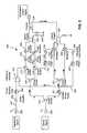
- FIG. 2illustrates a preferred embodiment 200 of the present invention.
- the circuit 200 shown in FIG. 2provides a new way to amplify and modulate the carrier signal in an AM RF transmitter.
- a baseband signalis introduced at input 202 and an RF carrier signal is introduced at input 204 .
- the carrier signalis split by a conventional power divider 214 into paths A and B. Following path A, the carrier signal is again divided into two paths by a second power divider 216 and then passed to a first phase shifter 212 and a second phase shifter 218 .
- the phase shifterschange the phase of the signals going into power amplifiers 224 , 226 and optional driver amplifiers 220 , 222 .
- the gain of the power amplifiers 224 , 226is controlled by individual control signals to ensure no excessive energy is wasted.
- Each power amplifier 224 , 226also receives a phase modulated input signal that is at a constant envelope, which allows the designer to use energy efficient nonlinear amplifiers without inducing excessive noise. If the signal input to the power amplifier were not constant (as in the case where the input signals were already modulated), then the amplifier would be dynamically adjusting its bias condition based on the input signal amplitude, with the result that the amplified signal would occupy a very wide frequency band (if nonlinear amplifiers are used). The wider frequency band includes more noise to the nearby radio frequency operated equipment.
- Amplitude modulationis achieved by combining the two amplified and phase modulated signals using a first combiner 228 , which in the exemplary embodiment shown is a hybrid coupler.
- a first combiner 228which in the exemplary embodiment shown is a hybrid coupler.
- One exemplary combineris a 3 dB 90° coupler.
- the combined signalwill vary from optimum when the phases are aligned, to a point where the signals might cancel portions of each other out when the phases are misaligned by 180 degrees.
- the phases of the two signalsare shifted in the opposite direction on a phase plane, equal in variation of angles.
- the in-phase sum of the two signalsbecomes the desired output, while the quadature sum becomes unwanted and goes into a dump 230 at the first combiner 228 . If the two phase shifters does not provide the same amount of phase shift, a residual phase shift is then created with the output signal.
- the total power output of the AM modulated output signalcan be precisely controlled by adjusting the amplifiers 220 , 222 , 224 , 226 and/or buffer amplifier 208 , so the spectrum of the AM modulated output signal can be made very sharp, in other words, made to occupy a very small spectrum.
- Thisenables, for example, RFID devices to function in a dense reader environment, where each reader may use a different spectrum for communications with tags. This also allows RFID devices to operate in jurisdictions where regulations only allow communications in a small bandwidth.
- An additional benefit of being able to use nonlinear amplifiers with adjustable gain to control the level of the AM modulated signal outputis that energy is conserved. Note that if energy conservation is not a concern, linear amplifiers could be used.
- the pulsecan be shaped to occupy a very narrow frequency band.
- An additional benefitis that by using two power amplifiers, each amplifier provides a constant power for each signal branch.
- the portion of the circuit described aboveis able to perform the modulation, but is not perfect. Accordingly, additional components are provided to further enhance the signal.
- a first feedback loop 232acts as a phase lock loop by extracting a portion of the AM modulated output signal at coupler 234 , combining it with the carrier input signal, and directing that back to the second phase shifter 218 .
- Thishas the effect of locking the AM modulated signal to the carrier input signal, thereby eliminating any residual phase variation (phase noise) in the AM modulated output signal. Accordingly, the phase change is used to create an AM modulated output which has virtually no phase noise.
- the carrier signalis the reference signal for the first feedback loop 232 .
- the carrier signalfollows path B and is split into two paths by a power divider 235 .
- a mixer/multiplier 236combines the extracted AM modulated signal with the carrier input signal.
- the carrier signalis compared to the AM modulated output to see if there is any phase difference between the two.
- a baseband signalis generated, which has a lower frequency compared to the carrier signal, but a similar or slightly higher frequency range than the AM modulated output. In other words, the frequency of the baseband signal is less than the frequency of the carrier signal, the carrier signal sometimes being referred to as the local oscillator signal.
- the baseband signalsets the modulator frequency.
- the AM output signalat best will have no residual phase shift. Ideally, its phase would follow the phase of a sine wave. If the phase loosens up during modulation, it will occupy a larger bandwidth.
- the multiplier 236acts as a phase detector that identifies the difference between the AM modulated output and the reference signal (carrier).
- the output signal from the mixer/multiplier 236continues on the first feedback loop 232 , where a loop amplifier 238 amplifies the signal, and a low pass filter 240 removes high frequency noise from the signal and stabilize the loop.
- the amplified and filtered signalis applied to the second phase shifter 218 , thereby controlling operation of the second phase shifter 218 .
- the first feedback loop 232automatically controls the second phase shifter 218 , with the result that the modulated signal at the output will have about the same phase as the input RF carrier signal.
- residual phase shiftis essentially removed.
- a variable delay line/phase shifter 241is placed on Path B before power divider 235 to ensure the stability of the system for a broad RF operating frequency band.
- the baseband signalaffects the first phase shifter 212 , changing the phase of the signals passing through the first phase shifter 212 by up to 180 degrees.
- the baseband signalis coupled through a conventional buffer amplifier 206 .
- a conventional pulse (spectrum) shaping filter 208provides a shaped input signal to a difference amplifier 210 .
- the difference amplifier 210in turn generates a control signal for controlling the first phase shifter 212 .
- an RF carrier signalis preferably modulated with a frequency limited baseband signal.
- a digital signal like the baseband signaloccupies a large frequency band. This signal needs to be shaped.
- a filter on the baseband input linewill not significantly limit the bandwidth of the baseband signal. Rather, some linearization is preferred.
- a problem solved by the embodiment shownis that the amplitude of the carrier signal does not otherwise follow linearly to the phase shifter control voltage.
- the non-linearitycomes from two aspects. One is from the control voltage-phase shift relationship of a reflective phase shifter, and the other is from the trigonometric combining of two RF signals. Assume a 1V phase shifter control signal applied to the first phase shifter creates a 10% shift. A 2V control input results in a 15% shift, and so on. This nonlinearity must be compensated for to obtain a clean AM output signal.
- the second feedback loop 242corrects the amplitude response to the phase shifter control voltage. In other words, the phase shifter control voltage is made linearly proportional to the amplitude of the AM modulated output signal.
- the carrier signalfollows path B, where a mixer/multiplier 244 combines the extracted AM modulated signal with the carrier input signal.
- This mixer/multiplieralso acts as the RF amplitude detector.
- the combined signalcontinues on the second feedback loop 242 , where an adjustable loop amplifier 246 amplifies the signal, and a low pass filter 248 filters the signal.
- the functions of the amplifier 246 and filter 248are similar to those of the filter 240 and amplifier 238 of the first feedback loop 232 .
- the amplifier 246is this case makes the feedback signal stronger so it becomes comparable to the baseband control signal.
- the baseband control signalis a 0 or 1 digitally, indicated by high and low signals or by length of high signal, length of low signal, etc.
- Typical high and low voltagesare 1 V and 4V, 0.5 V and 3V, etc.
- the adjustable nature of the amplifier 246allows the feedback signal (amplitude detector output) to be in about the same range as the baseband signal at the difference amplifier 210 .
- the amplified and filtered signalis directed to the difference amplifier 210 , which may be an operation amplifier.
- the difference amplifier 210develops a control signal by comparison of the shaped baseband signal and the envelope of the AM modulated output signal (amplitude detector signal) from the second feedback loop 242 . Any difference becomes the error signal output of the difference amplifier 210 , which is used to control the first phase shifter 212 .
- the second feedback loop 242acts as a linearization loop that directs some of the AM modulated output back to the difference amplifier 210 at the baseband signal input line 241 .
- This feedback schememakes the envelope amplitude of the AM modulated output signal linearly proportional to the amplitude of the baseband input signal by compensating for the non-linearity of the phase shifter response and phase modulation to amplitude modulation conversion.
- the second feedback loop 242may be either analog or digital.
- the phase of the first feedback loop 232is locked, and the second feedback loop 242 has a 90 degree phase shift from the first feedback loop 232 .
- the power divider 235 , multipliers 236 and 244 , and hybrid coupler 250form a quadature downconverter. All variations of quadature downconverters may be used here to detect the amplitude and phase of the modulated output.
- any form of power combinerincluding transformer, hybrid coupler, in-phase combiner and out-of-phase combiner, can be used to replace the power divider 216 , power divider 235 , hybrid coupler 228 and/or hybrid coupler 250 .
- the second feedback loop 242ensures that the amplitude of the AM output signal is linearly proportional to the baseband signal voltage. This in turn allows use of a simple filter in the baseband signal input line to define the spectrum.
Landscapes
- Amplifiers (AREA)
Abstract
Description
Claims (25)
Priority Applications (3)
| Application Number | Priority Date | Filing Date | Title |
|---|---|---|---|
| US11/207,348US7773695B2 (en) | 2005-08-19 | 2005-08-19 | Amplitude modulator |
| PCT/US2006/029629WO2007024416A2 (en) | 2005-08-19 | 2006-07-27 | Rfid reader and components thereof |
| US12/829,304US8064540B2 (en) | 2005-08-19 | 2010-07-01 | Amplitude modulator |
Applications Claiming Priority (1)
| Application Number | Priority Date | Filing Date | Title |
|---|---|---|---|
| US11/207,348US7773695B2 (en) | 2005-08-19 | 2005-08-19 | Amplitude modulator |
Related Child Applications (1)
| Application Number | Title | Priority Date | Filing Date |
|---|---|---|---|
| US12/829,304ContinuationUS8064540B2 (en) | 2005-08-19 | 2010-07-01 | Amplitude modulator |
Publications (2)
| Publication Number | Publication Date |
|---|---|
| US20070040606A1 US20070040606A1 (en) | 2007-02-22 |
| US7773695B2true US7773695B2 (en) | 2010-08-10 |
Family
ID=37766845
Family Applications (2)
| Application Number | Title | Priority Date | Filing Date |
|---|---|---|---|
| US11/207,348Active2029-02-22US7773695B2 (en) | 2005-08-19 | 2005-08-19 | Amplitude modulator |
| US12/829,304Expired - LifetimeUS8064540B2 (en) | 2005-08-19 | 2010-07-01 | Amplitude modulator |
Family Applications After (1)
| Application Number | Title | Priority Date | Filing Date |
|---|---|---|---|
| US12/829,304Expired - LifetimeUS8064540B2 (en) | 2005-08-19 | 2010-07-01 | Amplitude modulator |
Country Status (1)
| Country | Link |
|---|---|
| US (2) | US7773695B2 (en) |
Cited By (5)
| Publication number | Priority date | Publication date | Assignee | Title |
|---|---|---|---|---|
| US20100265043A1 (en)* | 2005-08-19 | 2010-10-21 | Liming Zhou | Amplitude modulator |
| US20100291869A1 (en)* | 2007-11-15 | 2010-11-18 | Robin Wilson | Near field rf communicators |
| US8577466B2 (en) | 2011-09-30 | 2013-11-05 | Nyxoah SA | System and method for nerve modulation using noncontacting electrodes |
| US9409013B2 (en) | 2009-10-20 | 2016-08-09 | Nyxoah SA | Method for controlling energy delivery as a function of degree of coupling |
| US9415216B2 (en) | 2009-10-20 | 2016-08-16 | Nyxoah SA | Devices for treatment of sleep apnea |
Families Citing this family (6)
| Publication number | Priority date | Publication date | Assignee | Title |
|---|---|---|---|---|
| SE0402571L (en)* | 2004-10-22 | 2005-09-27 | Cpum | RFID encoding |
| DE102006008790A1 (en)* | 2006-02-24 | 2007-09-06 | Infineon Technologies Ag | Modulation device for a transmission path, method for signal processing in a transmission path and transmission path with the modulation device |
| EP2234454B1 (en)* | 2009-03-24 | 2010-11-10 | Alcatel Lucent | A method for data transmission using an envelope elimination and restoration amplifier, an envelope elimination and restoration amplifier, a transmitting device, a receiving device and a communication network therefor |
| US8659357B1 (en) | 2012-08-01 | 2014-02-25 | Google Inc. | Conditionally-stable operational amplifier with tunable wideband buffers |
| RU2639942C1 (en)* | 2017-04-14 | 2017-12-25 | Акционерное общество "Научно-производственная корпорация "Системы прецизионного приборостроения" (АО "НПК "СПП") | High-sensitive amplitude detector |
| TWI831506B (en)* | 2022-12-07 | 2024-02-01 | 四零四科技股份有限公司 | Radio frequency filter with adjustable channel |
Citations (32)
| Publication number | Priority date | Publication date | Assignee | Title |
|---|---|---|---|---|
| US3896395A (en) | 1974-07-18 | 1975-07-22 | Bell Telephone Labor Inc | Linear amplification using quantized envelope components to phase reverse modulate quadrature reference signals |
| US4178557A (en) | 1978-12-15 | 1979-12-11 | Bell Telephone Laboratories, Incorporated | Linear amplification with nonlinear devices |
| US4574248A (en) | 1984-05-07 | 1986-03-04 | Rockwell International Corporation | RF Power amplifier for use with VHF transceivers |
| US5105164A (en) | 1989-02-28 | 1992-04-14 | At&T Bell Laboratories | High efficiency uhf linear power amplifier |
| US5249201A (en) | 1991-02-01 | 1993-09-28 | Mst, Inc. | Transmission of multiple carrier signals in a nonlinear system |
| US5321543A (en)* | 1992-10-20 | 1994-06-14 | General Instrument Corporation | Apparatus and method for linearizing an external optical modulator |
| US5365187A (en) | 1993-10-29 | 1994-11-15 | Hewlett-Packard Company | Power amplifier utilizing the vector addition of two constant envelope carriers |
| US5742201A (en) | 1996-01-30 | 1998-04-21 | Spectrian | Polar envelope correction mechanism for enhancing linearity of RF/microwave power amplifier |
| US5818298A (en) | 1994-01-11 | 1998-10-06 | Ericsson Inc. | Linear amplifying apparatus using coupled non-linear amplifiers |
| US5886573A (en) | 1998-03-06 | 1999-03-23 | Fujant, Inc. | Amplification using amplitude reconstruction of amplitude and/or angle modulated carrier |
| US6043707A (en) | 1999-01-07 | 2000-03-28 | Motorola, Inc. | Method and apparatus for operating a radio-frequency power amplifier as a variable-class linear amplifier |
| US6275685B1 (en) | 1998-12-10 | 2001-08-14 | Nortel Networks Limited | Linear amplifier arrangement |
| US6313703B1 (en) | 1998-06-19 | 2001-11-06 | Datum Telegraphic, Inc | Use of antiphase signals for predistortion training within an amplifier system |
| US6396341B1 (en) | 2000-12-29 | 2002-05-28 | Ericsson Inc. | Class E Doherty amplifier topology for high efficiency signal transmitters |
| US6472934B1 (en) | 2000-12-29 | 2002-10-29 | Ericsson Inc. | Triple class E Doherty amplifier topology for high efficiency signal transmitters |
| US20030045264A1 (en)* | 2001-08-29 | 2003-03-06 | Jeong Hei-Sam | Adaptive linearization technique for communication building block |
| US6567436B1 (en)* | 1999-01-26 | 2003-05-20 | California Institute Of Technology | Opto-electronic oscillators having optical resonators |
| US6583910B1 (en)* | 1998-04-27 | 2003-06-24 | Oki Electric Industry Co., Ltd. | Optical transmitter and optical communication system using the same |
| US20030189744A1 (en)* | 2002-04-05 | 2003-10-09 | Kelvin Prosyk | Re-circulating optical pulse generator |
| US20030194240A1 (en)* | 2002-04-10 | 2003-10-16 | Mollenauer Linn Frederick | Jitter compensation method and apparatus |
| US6639509B1 (en)* | 1998-03-16 | 2003-10-28 | Intermec Ip Corp. | System and method for communicating with an RFID transponder with reduced noise and interference |
| US20030223462A1 (en)* | 2002-05-31 | 2003-12-04 | Ar Card | Carrier-suppressed optical time domain multiplexing |
| US20040028146A1 (en)* | 2002-08-12 | 2004-02-12 | Clive Winkler | Method and apparatus for transferring multiple symbol streams at low bit-error rates in a narrowband channel |
| US6751265B1 (en)* | 2000-09-13 | 2004-06-15 | Tropian, Inc. | Method and system of amplitude modulation using dual/split channel unequal amplification |
| US6819174B2 (en) | 2002-03-28 | 2004-11-16 | Hitachi Kokusai Electric Inc. | Amplification device |
| US6825719B1 (en)* | 2000-05-26 | 2004-11-30 | Intel Corporation | RF power amplifier and methods for improving the efficiency thereof |
| US20040266368A1 (en)* | 2003-06-25 | 2004-12-30 | Nokia Corporation | Power control for a transmitter |
| US20040263246A1 (en)* | 2003-06-24 | 2004-12-30 | Ian Robinson | Multi-mode multi-amplifier architecture |
| US20050117191A1 (en)* | 2001-11-30 | 2005-06-02 | Robert Griffin | Modulation control |
| US20050136864A1 (en)* | 2003-12-17 | 2005-06-23 | Eliav Zipper | Radio frequency modulator and methods thereof |
| US20060083144A1 (en)* | 2004-10-19 | 2006-04-20 | Sioptical Inc. | Optical detector configuration and utilization as feedback control in monolithic integrated optic and electronic arrangements |
| US20070122161A1 (en)* | 2005-11-25 | 2007-05-31 | Alcatel | Fiber optical transmission system, transmitter and receiver for DQPSK modulated signals and method for stabilizing the same |
Family Cites Families (1)
| Publication number | Priority date | Publication date | Assignee | Title |
|---|---|---|---|---|
| US7773695B2 (en)* | 2005-08-19 | 2010-08-10 | Dominic Kotab | Amplitude modulator |
- 2005
- 2005-08-19USUS11/207,348patent/US7773695B2/enactiveActive
- 2010
- 2010-07-01USUS12/829,304patent/US8064540B2/ennot_activeExpired - Lifetime
Patent Citations (35)
| Publication number | Priority date | Publication date | Assignee | Title |
|---|---|---|---|---|
| US3896395A (en) | 1974-07-18 | 1975-07-22 | Bell Telephone Labor Inc | Linear amplification using quantized envelope components to phase reverse modulate quadrature reference signals |
| US4178557A (en) | 1978-12-15 | 1979-12-11 | Bell Telephone Laboratories, Incorporated | Linear amplification with nonlinear devices |
| US4574248A (en) | 1984-05-07 | 1986-03-04 | Rockwell International Corporation | RF Power amplifier for use with VHF transceivers |
| US5105164A (en) | 1989-02-28 | 1992-04-14 | At&T Bell Laboratories | High efficiency uhf linear power amplifier |
| US5249201A (en) | 1991-02-01 | 1993-09-28 | Mst, Inc. | Transmission of multiple carrier signals in a nonlinear system |
| US5321543A (en)* | 1992-10-20 | 1994-06-14 | General Instrument Corporation | Apparatus and method for linearizing an external optical modulator |
| US5365187A (en) | 1993-10-29 | 1994-11-15 | Hewlett-Packard Company | Power amplifier utilizing the vector addition of two constant envelope carriers |
| US5818298A (en) | 1994-01-11 | 1998-10-06 | Ericsson Inc. | Linear amplifying apparatus using coupled non-linear amplifiers |
| US5742201A (en) | 1996-01-30 | 1998-04-21 | Spectrian | Polar envelope correction mechanism for enhancing linearity of RF/microwave power amplifier |
| USRE37407E1 (en) | 1996-01-30 | 2001-10-16 | Spectrian Corporation | Polar envelope correction mechanism for enhancing linearity of RF/microwave power amplifier |
| US5886573A (en) | 1998-03-06 | 1999-03-23 | Fujant, Inc. | Amplification using amplitude reconstruction of amplitude and/or angle modulated carrier |
| US6147553A (en) | 1998-03-06 | 2000-11-14 | Fujant, Inc. | Amplification using amplitude reconstruction of amplitude and/or angle modulated carrier |
| US6639509B1 (en)* | 1998-03-16 | 2003-10-28 | Intermec Ip Corp. | System and method for communicating with an RFID transponder with reduced noise and interference |
| US6583910B1 (en)* | 1998-04-27 | 2003-06-24 | Oki Electric Industry Co., Ltd. | Optical transmitter and optical communication system using the same |
| US6313703B1 (en) | 1998-06-19 | 2001-11-06 | Datum Telegraphic, Inc | Use of antiphase signals for predistortion training within an amplifier system |
| US6275685B1 (en) | 1998-12-10 | 2001-08-14 | Nortel Networks Limited | Linear amplifier arrangement |
| US6043707A (en) | 1999-01-07 | 2000-03-28 | Motorola, Inc. | Method and apparatus for operating a radio-frequency power amplifier as a variable-class linear amplifier |
| US6567436B1 (en)* | 1999-01-26 | 2003-05-20 | California Institute Of Technology | Opto-electronic oscillators having optical resonators |
| US6825719B1 (en)* | 2000-05-26 | 2004-11-30 | Intel Corporation | RF power amplifier and methods for improving the efficiency thereof |
| US6751265B1 (en)* | 2000-09-13 | 2004-06-15 | Tropian, Inc. | Method and system of amplitude modulation using dual/split channel unequal amplification |
| US6472934B1 (en) | 2000-12-29 | 2002-10-29 | Ericsson Inc. | Triple class E Doherty amplifier topology for high efficiency signal transmitters |
| US6396341B1 (en) | 2000-12-29 | 2002-05-28 | Ericsson Inc. | Class E Doherty amplifier topology for high efficiency signal transmitters |
| US20030045264A1 (en)* | 2001-08-29 | 2003-03-06 | Jeong Hei-Sam | Adaptive linearization technique for communication building block |
| US20050117191A1 (en)* | 2001-11-30 | 2005-06-02 | Robert Griffin | Modulation control |
| US6819174B2 (en) | 2002-03-28 | 2004-11-16 | Hitachi Kokusai Electric Inc. | Amplification device |
| US20030189744A1 (en)* | 2002-04-05 | 2003-10-09 | Kelvin Prosyk | Re-circulating optical pulse generator |
| US20030194240A1 (en)* | 2002-04-10 | 2003-10-16 | Mollenauer Linn Frederick | Jitter compensation method and apparatus |
| US20030223462A1 (en)* | 2002-05-31 | 2003-12-04 | Ar Card | Carrier-suppressed optical time domain multiplexing |
| US20040028146A1 (en)* | 2002-08-12 | 2004-02-12 | Clive Winkler | Method and apparatus for transferring multiple symbol streams at low bit-error rates in a narrowband channel |
| US20040263246A1 (en)* | 2003-06-24 | 2004-12-30 | Ian Robinson | Multi-mode multi-amplifier architecture |
| US6853244B2 (en) | 2003-06-24 | 2005-02-08 | Northrop Grumman Corproation | Multi-mode multi-amplifier architecture |
| US20040266368A1 (en)* | 2003-06-25 | 2004-12-30 | Nokia Corporation | Power control for a transmitter |
| US20050136864A1 (en)* | 2003-12-17 | 2005-06-23 | Eliav Zipper | Radio frequency modulator and methods thereof |
| US20060083144A1 (en)* | 2004-10-19 | 2006-04-20 | Sioptical Inc. | Optical detector configuration and utilization as feedback control in monolithic integrated optic and electronic arrangements |
| US20070122161A1 (en)* | 2005-11-25 | 2007-05-31 | Alcatel | Fiber optical transmission system, transmitter and receiver for DQPSK modulated signals and method for stabilizing the same |
Non-Patent Citations (2)
| Title |
|---|
| PCT Preliminary Report from PCT application No. PCT/US2006/029629 mailed on Feb. 28, 2008. |
| PCT Search Report and Written Opinion from related PCT application No. PCT/US2006/029629 mailed on Mar. 28, 2007. |
Cited By (38)
| Publication number | Priority date | Publication date | Assignee | Title |
|---|---|---|---|---|
| US8064540B2 (en)* | 2005-08-19 | 2011-11-22 | Dominic Kotab | Amplitude modulator |
| US20100265043A1 (en)* | 2005-08-19 | 2010-10-21 | Liming Zhou | Amplitude modulator |
| US8588682B2 (en)* | 2007-11-15 | 2013-11-19 | Broadcom Innovision Limited | Near field RF communicators having refined energy sharing characterisitics utilizing improved shunt current control |
| US20100291869A1 (en)* | 2007-11-15 | 2010-11-18 | Robin Wilson | Near field rf communicators |
| US9197059B2 (en) | 2007-11-15 | 2015-11-24 | Broadcom Europe Limited | Near field RF communicators having refined energy sharing characteristics utilizing improved shunt current control |
| US9409013B2 (en) | 2009-10-20 | 2016-08-09 | Nyxoah SA | Method for controlling energy delivery as a function of degree of coupling |
| US8574164B2 (en) | 2009-10-20 | 2013-11-05 | Nyxoah SA | Apparatus and method for detecting a sleep disordered breathing precursor |
| US11273307B2 (en) | 2009-10-20 | 2022-03-15 | Nyxoah SA | Method and device for treating sleep apnea |
| US9943686B2 (en) | 2009-10-20 | 2018-04-17 | Nyxoah SA | Method and device for treating sleep apnea based on tongue movement |
| US8577472B2 (en) | 2009-10-20 | 2013-11-05 | Nyxoah SA | Systems and methods for determining a sleep disorder based on positioning of the tongue |
| US9550064B2 (en) | 2009-10-20 | 2017-01-24 | Adi Mashiach | Apparatus and methods for feedback-based nerve modulation |
| US9415215B2 (en) | 2009-10-20 | 2016-08-16 | Nyxoah SA | Methods for treatment of sleep apnea |
| US9415216B2 (en) | 2009-10-20 | 2016-08-16 | Nyxoah SA | Devices for treatment of sleep apnea |
| US8577464B2 (en) | 2009-10-20 | 2013-11-05 | Nyxoah SA | Apparatus and methods for feedback-based nerve modulation |
| US9248291B2 (en) | 2011-09-30 | 2016-02-02 | Adi Mashiach | Hypertension therapy implant apparatus |
| US9358392B2 (en) | 2011-09-30 | 2016-06-07 | Adi Mashiach | Electrode configuration for implantable modulator |
| US8798773B2 (en) | 2011-09-30 | 2014-08-05 | Man & Science, SA | Electrode configuration for implantable modulator |
| US8929999B2 (en) | 2011-09-30 | 2015-01-06 | Adi Maschiach | Electrode configuration for implantable modulator |
| US8989868B2 (en) | 2011-09-30 | 2015-03-24 | Hyllio SA | Apparatus and method for controlling energy delivery as a function of degree of coupling |
| US9044612B2 (en) | 2011-09-30 | 2015-06-02 | Adi Mashiach | Apparatus and method for extending implant life using a dual power scheme |
| US9061151B2 (en) | 2011-09-30 | 2015-06-23 | Adi Mashiach | Apparatus and method to control an implant |
| US8700183B2 (en) | 2011-09-30 | 2014-04-15 | Nyxoah SA | Devices and methods for low current neural modulation |
| US8644957B2 (en) | 2011-09-30 | 2014-02-04 | Nyxoah SA | Electrode configuration for implantable modulator |
| US9302093B2 (en) | 2011-09-30 | 2016-04-05 | Nyxoah SA | Devices and methods for delivering energy as a function of condition severity |
| US9314613B2 (en) | 2011-09-30 | 2016-04-19 | Adi Mashiach | Apparatus and methods for modulating nerves using parallel electric fields |
| US8718776B2 (en) | 2011-09-30 | 2014-05-06 | Nyxoah SA | Apparatus and method to control an implant |
| US9403009B2 (en) | 2011-09-30 | 2016-08-02 | Nyxoah SA | Apparatus and methods for implant coupling indication |
| US8577466B2 (en) | 2011-09-30 | 2013-11-05 | Nyxoah SA | System and method for nerve modulation using noncontacting electrodes |
| US8577468B2 (en) | 2011-09-30 | 2013-11-05 | Nyxoah SA | Apparatus and method for extending implant life using a dual power scheme |
| US8588941B2 (en) | 2011-09-30 | 2013-11-19 | Nyxoah SA | Device and method for modulating nerves using parallel electric fields |
| US9421372B2 (en) | 2011-09-30 | 2016-08-23 | Adi Mashiach | Head pain management device having an antenna |
| US8577465B2 (en) | 2011-09-30 | 2013-11-05 | Nyxoah SA | Modulator apparatus configured for implantation |
| US9649493B2 (en) | 2011-09-30 | 2017-05-16 | Adi Mashiach | System and method for nerve modulation using noncontacting electrodes |
| US9878159B2 (en) | 2011-09-30 | 2018-01-30 | Adi Mashiach | Hypertension therapy implant apparatus |
| US9895540B2 (en) | 2011-09-30 | 2018-02-20 | Nyxoah SA | Devices and methods for low current neural modulation |
| US8577467B2 (en) | 2011-09-30 | 2013-11-05 | Nyxoah SA | Apparatus and method for controlling energy delivery as a function of degree of coupling |
| US10828492B2 (en) | 2011-09-30 | 2020-11-10 | Adi Mashiach | Devices and methods for low current neural modulation |
| US8577478B2 (en) | 2011-09-30 | 2013-11-05 | Nyxoah SA | Antenna providing variable communication with an implant |
Also Published As
| Publication number | Publication date |
|---|---|
| US20070040606A1 (en) | 2007-02-22 |
| US20100265043A1 (en) | 2010-10-21 |
| US8064540B2 (en) | 2011-11-22 |
Similar Documents
| Publication | Publication Date | Title |
|---|---|---|
| US8064540B2 (en) | Amplitude modulator | |
| US11115083B2 (en) | Direct conversion polar transmitter for an RFID reader | |
| US8180304B2 (en) | Efficient power amplifier | |
| US20070066224A1 (en) | High efficiency RF amplifier and envelope modulator | |
| US8290452B2 (en) | Radio frequency transmitter and signal amplification method therefor | |
| US6631254B1 (en) | Apparatus for producing a radio-frequency signal | |
| EP2285059A3 (en) | Digital transmitters for wireless communication | |
| US20050143026A1 (en) | Integrated switching device for routing radio frequency signals | |
| WO2014042270A1 (en) | Transmitter | |
| US6917791B2 (en) | Polar loop transmitter | |
| KR100799227B1 (en) | Cascode Structured Power Amplifier for Amplitude Modulation | |
| CN101816129A (en) | Multiple transmission apparatus with reduced coupling | |
| US6690743B1 (en) | Compensation of delay in linearization loop of power amplifier | |
| US6687312B1 (en) | Signal processing system | |
| US20050221772A1 (en) | Harmonic mixer and radio communication device having the same | |
| US10298428B2 (en) | Wireless transmission device and wireless transmission method | |
| US20210367606A1 (en) | Apparatus and method for frequency multiplication | |
| US7062231B2 (en) | Direct modulation transmitter utilizing signals squaring | |
| US7528699B2 (en) | Transponder in communication system | |
| KR100862524B1 (en) | Voltage controlled oscillator | |
| JP4391291B2 (en) | Wireless device | |
| JP2009129173A (en) | Transmitter | |
| JP5053310B2 (en) | Transceiver circuit and signal receiving method thereof | |
| KR101231381B1 (en) | Phase compensation system | |
| TW200729869A (en) | Digital transmitters for wireless communication |
Legal Events
| Date | Code | Title | Description |
|---|---|---|---|
| AS | Assignment | Owner name:APPLIED WIRELESS IDENTIFICATION GROUP, INC., CALIF Free format text:ASSIGNMENT OF ASSIGNORS INTEREST;ASSIGNORS:ZHOU, LIMING;KIKIN, VADIM;REEL/FRAME:016880/0203 Effective date:20050816 | |
| AS | Assignment | Owner name:EMMT SYSTEMS CORP., TAIWAN Free format text:SECURITY AGREEMENT;ASSIGNOR:APPLIED WIRELESS IDENTIFICATIONS GROUP, INC.;REEL/FRAME:019047/0666 Effective date:20061017 | |
| AS | Assignment | Owner name:KOTAB, DOMINIC, CALIFORNIA Free format text:ASSIGNMENT OF ASSIGNORS INTEREST;ASSIGNOR:APPLIED WIRELESS IDENTIFICATION GROUP, INC.;REEL/FRAME:022795/0074 Effective date:20090602 | |
| STCF | Information on status: patent grant | Free format text:PATENTED CASE | |
| FPAY | Fee payment | Year of fee payment:4 | |
| MAFP | Maintenance fee payment | Free format text:PAYMENT OF MAINTENANCE FEE, 8TH YEAR, LARGE ENTITY (ORIGINAL EVENT CODE: M1552) Year of fee payment:8 | |
| MAFP | Maintenance fee payment | Free format text:PAYMENT OF MAINTENANCE FEE, 12TH YEAR, LARGE ENTITY (ORIGINAL EVENT CODE: M1553); ENTITY STATUS OF PATENT OWNER: LARGE ENTITY Year of fee payment:12 | |
| AS | Assignment | Owner name:NETMOMENTUM LLC, NEW MEXICO Free format text:ASSIGNMENT OF ASSIGNORS INTEREST;ASSIGNOR:NETMOMENTUM LLC;REEL/FRAME:069327/0465 Effective date:20240531 |