US7772866B2 - Structure and method of mapping signal intensity to surface voltage for integrated circuit inspection - Google Patents
Structure and method of mapping signal intensity to surface voltage for integrated circuit inspectionDownload PDFInfo
- Publication number
- US7772866B2 US7772866B2US11/683,058US68305807AUS7772866B2US 7772866 B2US7772866 B2US 7772866B2US 68305807 AUS68305807 AUS 68305807AUS 7772866 B2US7772866 B2US 7772866B2
- Authority
- US
- United States
- Prior art keywords
- transistors
- voltage
- test structure
- structure according
- group
- Prior art date
- Legal status (The legal status is an assumption and is not a legal conclusion. Google has not performed a legal analysis and makes no representation as to the accuracy of the status listed.)
- Expired - Fee Related, expires
Links
Images


Classifications
- H—ELECTRICITY
- H01—ELECTRIC ELEMENTS
- H01L—SEMICONDUCTOR DEVICES NOT COVERED BY CLASS H10
- H01L22/00—Testing or measuring during manufacture or treatment; Reliability measurements, i.e. testing of parts without further processing to modify the parts as such; Structural arrangements therefor
- H01L22/30—Structural arrangements specially adapted for testing or measuring during manufacture or treatment, or specially adapted for reliability measurements
- H01L22/34—Circuits for electrically characterising or monitoring manufacturing processes, e. g. whole test die, wafers filled with test structures, on-board-devices incorporated on each die, process control monitors or pad structures thereof, devices in scribe line
- H—ELECTRICITY
- H01—ELECTRIC ELEMENTS
- H01L—SEMICONDUCTOR DEVICES NOT COVERED BY CLASS H10
- H01L22/00—Testing or measuring during manufacture or treatment; Reliability measurements, i.e. testing of parts without further processing to modify the parts as such; Structural arrangements therefor
Definitions
- the present inventionrelates generally to the manufacturing of semiconductor devices. More specifically, it relates to methods and structures used in mapping a signal intensities measured during inspection of integrated circuit to surface voltages of semiconductor devices on a semiconductor wafer.
- processingmay include, for example, ion implantation and/or doping, chemical vapor deposition, isotropic and/or anisotropic etching, chemical-mechanical-polishing, etc.
- the processingmay produce devices such as, for example, field-effect-transistor (FET), electronic fuse, random access memory (RAM), etc.
- FETfield-effect-transistor
- RAMrandom access memory
- non-destructive and/or in-situ testing at different processing stagesis essential and generally preferred.
- a non-destructive in-site testingmay timely provide vital information on processing conditions that may need to be adjusted during the course of manufacturing in order to control the quality of the final products, and to monitor possible development of device defects.
- Non-destructive and/or in-site testingmay be conducted directly on semiconductor devices in a wafer under development. Alternatively, it may be performed in one or more designated testing areas or testing strips on the same wafer whereupon the semiconductor devices are commonly produced.
- a testing stripmay include one or more test structures embedded in between the semiconductor devices in order to closely resemble processing conditions experienced by the semiconductor devices. It is also conceivable that a test strip may be formed in a wafer different from that of the semiconductor devices but the test strip is placed closely to the wafer of the semiconductor devices during manufacturing and testing.
- a surface voltage testing mechanismwhich measures device parameters that may be used as a general indication as to the quality of electrical nodes and/or contacts often found in various semiconductor devices.
- Kelvin probeis a non-contact, non-destructive measurement device used to investigate properties of materials.
- a Kelvin probebased on a vibrating capacitor, generally measures a difference in work functions (or for non-metals surface potentials) between a conducting specimen and a vibrating tip.
- the work functionis extremely sensitive to the surface conditions and thus its reading may be adversely affected by, for example, absorbed or evaporated layers, surface reconstruction, surface charging, oxide layer imperfections, surface and bulk contamination, etc., to list a few. Because the work function is so sensitive, it is sometimes difficult to make proper differentiation and/or judgment between a voltage difference caused by actual conditions of the semiconductor device under test and that caused by changes in one or more of the many affecting factors.
- Embodiments of the present inventionprovide a test structure fabricated together with one or more integrated circuits on a semiconductor wafer.
- the test structuremay include a common reference point for voltage reference; one or more voltage dropping devices connected to the common reference point; and one or more electron-collecting pads connected to one or more contact points of the voltage dropping devices.
- a brightness shown by the one or more electron-collecting pads during an inspection of the integrated circuitsmay be associated with or mapped to a pre-determined voltage.
- the common reference pointmay be, for example, a ground point which has a known fixed voltage, such as zero, during the inspection of the integrated circuits.
- the voltage dropping devicesmay be a group of diodes with the contact points being the anode thereof.
- the group of diodesmay be connected in a series with the cathode of a diode being connected to the anode of a preceding diode.
- the first diode in the seriesmay be connected to the common reference point.
- the voltage dropping devicesmay be a group of transistors with a gate of the transistors being connected to either a source or a drain of said transistors, depending on the type of the transistors.
- the transistorsmay have a pre-defined or pre-determined voltage drop from the source to the drain during operation.
- the transistorsmay be connected in a series with the drain of a transistor being connected to the source of an adjacent transistor.
- Embodiments of the present inventionalso provide a test structure formed or fabricated upon a semiconductor wafer having one or more integrated circuits.
- the test structuremay include a common reference point for voltage reference; a plurality of voltage dropping devices having respectively a first and a second contact point with the first contact point being associated with the common reference point.
- the voltage dropping devicesmay be adapted to hold up to a certain pre-determined value of voltages between the first and second contact points respectively, and a plurality of conductive pads being connected to the second points of the voltage dropping devices respectively.
- the conductive padsmay be adapted to hold electronic charges during an inspection of the integrated circuits.
- the plurality of voltage dropping devicesmay be a group of semiconductor diodes, with the first contact point being the anode and the second contact point being the cathode, connected in a series with the cathode of a diode being connected to the anode of a neighboring diode except that the first diode in the series is connected to the common reference point.
- the plurality of voltage dropping devicesmay be a group of transistors with a gate being connected to a source or a drain depending on the type of the transistors.
- the transistorshave a pre-determined voltage drop from the source to the drain during operation.
- the group of transistorsmay be connected in a series with the drain of a transistor being connected to the source of an adjacent transistor.
- Embodiments of the present inventionmay further provide a structure that includes a substrate having a ground point; a plurality of semiconductor devices having respectively first and second contact points; and the first contact points being associated with the ground point.
- the semiconductor devicesmay be adapted to hold, up to a pre-determined set of values of, voltages between the first and second contact points.
- a plurality of conductive padsmay be connected to the second contact points of the semiconductor devices respectively, and may be adapted to collect electronic charges during an inspection of one or more integrated circuits.
- FIG. 1is a sample SEM image of a SRAM array as is known in the prior art
- FIG. 2is a demonstrative illustration of a test structure according to one embodiment of the present invention.
- FIG. 3is a demonstrative illustration of a transistor structure having a pre-determined voltage drop from a source to a drain and is suitable for embodiments of the present invention
- FIG. 4A and FIG. 4Bare demonstrative illustrations of a test structure according to another embodiment of the present invention.
- FIG. 5is a demonstrative illustration of a test structure according to yet another embodiment of the present invention.
- FIG. 6is a sample SEM image using test structures according to one embodiment of the present invention.
- FIG. 1is a sample SEM image of a static random access memory (SRAM) array. This SRAM array image 100 was taken after being tungsten (W) chemical-mechanical-polished (WCMP) as is known in the art.
- Wtungsten
- WCMPchemical-mechanical-polished
- Image 100shows that various contacts (e.g., contact 101 ) that land on one or more p-type field-effect-transistors (PFETs) are grounded and therefore appear relatively bright, while other contacts (e.g., contact 102 ) that land on one or more n-type field-effect-transistors (NFETs) are floating and therefore appear relatively dark.
- PFETsp-type field-effect-transistors
- NFETsn-type field-effect-transistors
- the exact intensity or brightness of a floating structurevaries with the actual potential or voltage of the node. The higher the voltage, the darker the node usually appears.
- a contact on the nodeis open or short. This is because certain defects may not cause absolute opens or shorts and instead may show resistive characteristics. Knowing surface voltages on either side of a defect may enable the resistance associated therewith to be properly determined or estimated.
- surface voltagemay be used to determine performance characteristics of a transistor.
- information on surface voltagemay be used to calibrate a model of the voltage contrast process which could be used to select the optimal conditions for different inspections.
- embodiment of the present inventionprovides a test structure that may include a set of electronic devices such as, for example, semiconductor diodes (or transistors) with approximately the same pre-defined or pre-determined voltage drops.
- the set of electronic devicesmay be arranged in a series to form a set of electrical testing nodes with known voltages.
- a set of electronic devices with different and incremental pre-defined or pre-determined voltage dropsmay be arranged in parallel, with a common voltage reference point, to form a set of electrical testing nodes.
- the test structure, having the set of electrical testing nodesmay be formed in a testing area or testing strip preferably created in a wafer common to the semiconductor devices under test.
- the test structuremay also be formed in a wafer separate and different from the wafer containing the semiconductor devices.
- the signal intensity detected at a contact or node of a semiconductor devicemay be mapped to a corresponding surface voltage by referring to a map generated from a set of signal intensities associated with the set of electrical testing nodes formed in the testing area or testing strip.
- the test structuremay be placed in close proximity to the wafer having the semiconductor devices during the device manufacturing process such that the test structure may experience similar processing conditions as those of the semiconductor devices.
- FIG. 2is a demonstrative illustration of a test structure according to one embodiment of the present invention.
- Test structure 200may be used to properly determine the surface voltage of a node of resistive characteristics.
- Test structure 200may include a set of voltage dropping devices such as, for example, semiconductor diodes 211 , 212 , 213 , 214 , 215 and 216 that are connected in a series and ultimately to a common reference point 210 . More specifically, the anode of one diode, e.g., diode 213 , may be connected to the cathode of the next diode, e.g., diode 214 .
- the cathode of diode 214may be connected to the anode of the preceding diode 213 .
- Cathode of the first diode in the seriesi.e., diode 211
- the common reference point 210which may be a ground point 210 .
- Connection to common reference point 210may provide a voltage reference point for the diode series.
- diodes 211 , 212 , 213 , 214 , 215 and 216may be fabricated from a substantially same semiconductor material; have a substantially same structure; and thus a substantially same voltage drop, which in this case may be the bias voltage (threshold voltage) across their respective p-n junctions, during operation.
- the term “substantially” or “approximately”may be applied to modify any quantitative representation which could permissibly vary without resulting in a change in the basic function to which it is related).
- semiconductor diode 211 , and other semiconductor diodes 212 - 216may be formed to have a bias voltage of approximate 0.6V across its p-n junction.
- bias voltagemay depend on the types of dopants and the doping concentration used during the fabrication of the semiconductor diodes.
- Test structure 200may also include a set of pads 220 , 221 , 222 , 223 , 224 , 225 and 226 , of substantially the same sizes and shapes, connected to the anodes of their respective diodes 211 , 212 , 213 , 214 , 215 and 216 except for the first pad 220 , which may be connected directly to common reference point 210 .
- Pads 220 - 226may be made of conductive or semi-conductive materials such as, for example, nickel silicide (NiSi) and may be used to collect electrons, during a voltage contrast inspection using SEM. For that reason, pads 220 - 226 may be referred to as “electron-collecting pad” or “conductive pad” throughout this application.
- an electron-collecting pade.g., pad 223
- an electron-collecting padmay be able to collect electrons until a voltage potential created by the accumulatively collected electrons is either clamped by a threshold voltage of the semiconductor diode, e.g., diode 213 to which pad 223 is connected, or limited by a leakage current associated with pad 223 .
- a threshold voltage of the semiconductor diodee.g., diode 213 to which pad 223 is connected
- a leakage current associated with pad 223e.g., a threshold voltage of the semiconductor diode, e.g., diode 213 to which pad 223 is connected, or limited by a leakage current associated with pad 223 .
- the voltage potential that may be held by pad 223will be mainly limited by the threshold voltage that turns diode 213 on, which will be equal to the accumulative voltage drops across diode 213 and all the preceding diodes 211 and 212 .
- electron-collecting pad 221may be charged up to 0.6V; electron-collecting pad 222 may be up to 1.2V; electron-collecting pad 223 may be up to 18V, etc.
- the chain of semiconductor diodes 211 - 216thus may provide a granularity of 0.6V for voltage detection.
- FIG. 2a person skilled in the art may appreciate that although a set of six (6) semiconductor diodes and a set of six (6) corresponding electron-collecting pads are illustrated in FIG. 2 , the present invention is not limited in this respect and other number of diodes and pads, other than six (6), may be used as well. A person skilled in the art may also appreciate that, depending on the range of interest in the voltage under detection, some of the diodes may not necessarily have electron-collecting pads connected thereto. Also, as described above, the electron-collecting pads 220 - 226 may have any other suitable shapes and the rectangular shape shown in FIG. 1 is for illustration purpose.
- FIG. 2a set of voltage drops that may be held by electron-collecting pads 221 - 226 is illustrated to be provided by a set of cascaded semiconductor diodes 211 - 216 .
- the present inventionis not limited in this respect.
- Other voltage dropping devicesmay be used in replacement of diode 211 - 216 .
- FIG. 3is a demonstrative illustration of a transistor 300 such as, for example, a field-effect-transistor (FET) with its source 301 and gate 303 connected together.
- Transistor 300may provide a pre-defined or pre-determined voltage drop, for example 0.15V, from source 301 to drain 302 during operation.
- FETfield-effect-transistor
- Transistor 300may be used to replace one or more diodes 211 - 216 as shown in FIG. 2 .
- the relatively small voltage drop of around 0.15V from source 301 to drain 302compared with 0.6V of the semiconductor diodes 211 - 216 shown in FIG. 2 , may provide a better granularity and/or higher resolution during a voltage contrast inspection of semiconductor devices.
- Electron-collecting pads 221 - 226 and semiconductor diodes 211 - 216may be manufactured at a same metal level or different metal levels during the process of semiconductor manufacturing. If being manufactured or formed at different metal levels, electron-collecting pads 221 - 226 may be connected to the anodes of their respective semiconductor diodes 211 - 216 through inter-connect structures built into inter-level dielectric (ILD) layers. Inter-connect structures between different metal levels and process of forming the same are well known in the art and therefore are not described here for clarity purpose.
- ILDinter-level dielectric
- electronsmay accumulate on structures such as contacts and/or metal runners, for example a node which may be grounded, semi-grounded, or floating, of semiconductor devices. In the mean time, electrons may also accumulate on one or more electron-collecting pads in a test structure according to embodiments of the present invention. As is shown in the SEM image of FIG. 1 , usually a grounded structure appears bright and a floating structure appears dark. The brightness shown in the SEM image of FIG. 1 may reflect a particular voltage relating to a particular point or element under test. According to one embodiment of the present invention, the brightness of a particular element under test may be compared to those of the electron-collecting pads in the test structure.
- the element under testmay be a gate or active region.
- the element under testmay be different contacts.
- the element under testmay be different metal elements. Since voltages supported by each individual electron-collecting pads are associated by the diodes that they are connected to and so the values of the voltages are pre-defined or pre-determined, the brightness of the contact under test may be associated to a particular voltage. The comparison of brightness may be conducted visually for relatively coarse granularity, or through other advanced techniques for better granularity. For example, a computer system may be configured or programmed to compare the brightness of pixels based on their corresponding grey scales.
- the grey scalesmay be represented by a range of numerical figures, for example, from 1 to 1024. Furthermore, for example, assuming the brightness of an electron-collecting pad having a surface voltage 0.6V is represented by a numerical grey scale 213 , any pixels in the detected image from the circuit of interest having the same numerical grey scale 213 may indicates a surface voltage of 0.6V. It shall be noted that at some stages of the device manufacturing, for example, at a stage after the gate stack formation, the surface may contain or be covered by different conductive materials (e.g. a poly gate and crystalline silicon active regions), which may cause certain variation in the brightness of the circuit under test. Therefore, some brightness calibration may be needed.
- conductive materialse.g. a poly gate and crystalline silicon active regions
- FIG. 4Ais a demonstrative illustration of a test structure according to another embodiment of the present invention.
- Test structure 400may include a set of transistors (e.g., NFET and/or PFET) 411 , 412 , 413 and 414 , having different but pre-determined threshold voltages (VT) during operation.
- FIG. 4Bis an illustrative top view of one possible layout of the set of transistors shown in FIG. 4A .
- the number of transistors, four (4)are selected for illustration purpose only.
- the present inventionis not limited in this respect and other number of transistors, such as six (6), eight (8), or ten (10), may be used as well.
- a transistorusually comprises three regions including a source, a drain, and a gate.
- transistors 411 , 412 , 413 , and 414may be n-type transistors (e.g., NFET) and sources of transistors 411 , 412 , 413 , and 414 may be connected in parallel to a common reference point 410 , for example, a ground point. Drains of transistors 411 , 412 , 413 , and 414 may be connected to a set of electron-collecting pads 421 , 422 , 423 , and 424 .
- transistors 411 , 412 , 413 , and 414may be p-type transistors (e.g., PFET) and drains of transistors 411 , 412 , 413 , and 414 may be connected in parallel to common reference point 410 and sources of transistors 411 , 412 , 413 , and 414 may be connected to the set of electron-collecting pads 421 , 422 , 423 , and 424 .
- gates of transistors 411 , 412 , 413 , and 414may be connected to a testing point 420 , which may be an electron-collecting pad.
- transistors 411 , 412 , 413 , and 414may have different gate width, therefore resulting in different but pre-determined threshold voltages.
- voltages at the gate of one or more transistors 411 , 412 , 413 , and 414may exceed their respective threshold, turn the transistor on, and result in electrons collected at corresponding electron-collecting pads to flow towards the common reference point 410 .
- the corresponding electron-collecting padmay have a voltage potential that is close to that of common reference point 410 .
- conductive pads 421 and 422may have a near zero voltage (or a voltage close to the voltage drop between source and drain of transistors 411 and 412 ) and may thus appear bright in an SEM image during a voltage contrast inspection.
- the surface voltage of testing node 420in the above example, may be determined to be above the threshold voltages of transistors 411 and 412 but below the threshold voltages of transistors 413 and 414 by simply identifying which conductive pad is bright.
- a set of testing structure 400 with different sizes of testing node 420may be formed in a testing area or testing strip.
- the testing nodes of different sizesmay hold different surface voltages, whose value may be determined by looking at the number of transistors that are turned on, to provide a map between brightness and voltages. The map may then be used to properly determine surface voltages of contacts and/or nodes of semiconductor devices under test. The surface voltages are in general associated with the quality of the contacts and/or nodes.
- a scheme of testing structure 400generally provides a better sensitivity when compared with a scheme shown in FIG. 2 , with the resolution not being limited by the minimum voltage drop across one diode. On the other hand, it generally requires more spaces in the testing area or testing strip since a plurality of such testing structures, like testing structure 400 , may need to be fabricated.
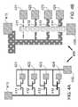
- FIG. 5is a demonstrative illustration of a test structure according to another embodiment of the present invention.
- Test structure 500may include a plurality of groups of transistor/pad pair, such as for example groups 521 , 522 , 523 , and 524 , as well as a testing node 520 .
- Each group, for example group 521may include a first transistor/pad pair 521 A and a second transistor/pad pair 521 B.
- the first transistor/pad pair 521 Amay correspond to transistor 411 and electron-collecting pad 421 in FIG. 4 .
- the second transistor/pad pair 521 Bmay be supplemental to the first transistor/pad pair 521 A to allow the threshold voltage of associated transistor to be measured and/or calibrated using an in-line or end of line tester.
- FIG. 1is a demonstrative illustration of a test structure according to another embodiment of the present invention.
- Test structure 500may include a plurality of groups of transistor/pad pair, such as for example groups 521 , 522 , 523 ,
- second group 522having a first and a second transistor/pad pair 522 A and 522 B
- third group 523having a first and a second transistor/pad pair 523 A and 523 B
- fourth group 524having a first and a second transistor/pad pair 524 A and 524 B.
- FIG. 6is a sample SEM image of a test structures according to one embodiment of the present invention.
- Test area 600 in FIG. 6may include two test structures 610 and 620 and according to one embodiment of the present invention test structures 610 and 620 may be replicates of a same structure.
- test structure 610may include a plurality of semiconductor diodes, for example, 611 , 612 , 613 , 614 , 615 , and 616 which maybe semiconductor diodes as described above with regard to FIG. 2 .
- the various spots of different brightnessillustrate electron-collecting pads under different potentials with the biggest and brightest spot to the most right being a ground point 619 .
- Diodes 611 - 614are arranged to point in the direction of the ground 619 ; meaning anodes of diodes 611 - 614 are further away from ground point 619 than their respective cathodes. Because brightness of the electron-collecting pads represent surface voltages at locations between points 619 and 611 , between points 611 and 612 , between points 612 and 613 , and between points 613 and 614 , a person skilled in the art may appreciate that FIG. 6 provides a clear indication that the respective diodes are turned on and the voltage is different in each of these locations.
- semiconductor diodes 615 and 616are pointed away from ground point 619 ; meaning cathodes of diodes 615 and 616 are further away from ground 619 than their respective anodes. Diodes 615 and 616 may provide certain intensity mapping capability when electron retarding conditions, where a negative potential is induced on floating surface elements, occurs.
Landscapes
- Engineering & Computer Science (AREA)
- Manufacturing & Machinery (AREA)
- Computer Hardware Design (AREA)
- Microelectronics & Electronic Packaging (AREA)
- Power Engineering (AREA)
- Automation & Control Theory (AREA)
- Testing Or Measuring Of Semiconductors Or The Like (AREA)
Abstract
Description
Claims (20)
Priority Applications (2)
| Application Number | Priority Date | Filing Date | Title |
|---|---|---|---|
| US11/683,058US7772866B2 (en) | 2007-03-07 | 2007-03-07 | Structure and method of mapping signal intensity to surface voltage for integrated circuit inspection |
| KR1020080004031AKR101365193B1 (en) | 2007-03-07 | 2008-01-14 | Structure and method of mapping signal intensity to surface voltage for integrated circuit inspection |
Applications Claiming Priority (1)
| Application Number | Priority Date | Filing Date | Title |
|---|---|---|---|
| US11/683,058US7772866B2 (en) | 2007-03-07 | 2007-03-07 | Structure and method of mapping signal intensity to surface voltage for integrated circuit inspection |
Publications (2)
| Publication Number | Publication Date |
|---|---|
| US20080217612A1 US20080217612A1 (en) | 2008-09-11 |
| US7772866B2true US7772866B2 (en) | 2010-08-10 |
Family
ID=39740735
Family Applications (1)
| Application Number | Title | Priority Date | Filing Date |
|---|---|---|---|
| US11/683,058Expired - Fee RelatedUS7772866B2 (en) | 2007-03-07 | 2007-03-07 | Structure and method of mapping signal intensity to surface voltage for integrated circuit inspection |
Country Status (2)
| Country | Link |
|---|---|
| US (1) | US7772866B2 (en) |
| KR (1) | KR101365193B1 (en) |
Cited By (17)
| Publication number | Priority date | Publication date | Assignee | Title |
|---|---|---|---|---|
| US8750597B2 (en) | 2011-11-23 | 2014-06-10 | International Business Machines Corporation | Robust inspection alignment of semiconductor inspection tools using design information |
| US20160356750A1 (en)* | 2015-06-05 | 2016-12-08 | Semilab SDI LLC | Measuring semiconductor doping using constant surface potential corona charging |
| US9627370B1 (en) | 2016-04-04 | 2017-04-18 | Pdf Solutions, Inc. | Integrated circuit containing standard logic cells and library-compatible, NCEM-enabled fill cells, including at least via-open-configured, GATE-short-configured, GATECNT-short-configured, and TS-short-configured, NCEM-enabled fill cells |
| US9691672B1 (en) | 2015-12-16 | 2017-06-27 | Pdf Solutions, Inc. | Integrated circuit containing standard logic cells and library-compatible, NCEM-enabled fill cells, including at least via-open-configured, GATE-short-configured, GATECNT-short-configured, and metal-short-configured, NCEM-enabled fill cells |
| US9721938B1 (en) | 2016-04-04 | 2017-08-01 | Pdf Solutions, Inc. | Integrated circuit containing first and second DOEs of standard cell compatible, NCEM-enabled fill cells, with the first DOE including tip-to-tip short configured fill cells, and the second DOE including corner short configured fill cells |
| US9748153B1 (en) | 2017-03-29 | 2017-08-29 | Pdf Solutions, Inc. | Process for making and using a semiconductor wafer containing first and second does of standard cell compatible, NCEM-enabled fill cells, with the first DOE including side-to-side short configured fill cells, and the second DOE including tip-to-side short configure |
| US9768083B1 (en) | 2017-06-27 | 2017-09-19 | Pdf Solutions, Inc. | Process for making and using a semiconductor wafer containing first and second DOEs of standard cell compatible, NCEM-enabled fill cells, with the first DOE including merged-via open configured fill cells, and the second DOE including snake open configured fill cells |
| US9773774B1 (en) | 2017-03-30 | 2017-09-26 | Pdf Solutions, Inc. | Process for making and using a semiconductor wafer containing first and second DOEs of standard cell compatible, NCEM-enabled fill cells, with the first DOE including chamfer short configured fill cells, and the second DOE including corner short configured fill cells |
| US9786649B1 (en) | 2017-06-27 | 2017-10-10 | Pdf Solutions, Inc. | Process for making and using a semiconductor wafer containing first and second DOEs of standard cell compatible, NCEM-enabled fill cells, with the first DOE including via open configured fill cells, and the second DOE including stitch open configured fill cells |
| US9805994B1 (en) | 2015-02-03 | 2017-10-31 | Pdf Solutions, Inc. | Mesh-style NCEM pads, and process for making semiconductor dies, chips, and wafers using in-line measurements from such pads |
| US9865583B1 (en) | 2017-06-28 | 2018-01-09 | Pdf Solutions, Inc. | Process for making and using a semiconductor wafer containing first and second DOEs of standard cell compatible, NCEM-enabled fill cells, with the first DOE including snake open configured fill cells, and the second DOE including stitch open configured fill cells |
| US9929063B1 (en) | 2016-04-04 | 2018-03-27 | Pdf Solutions, Inc. | Process for making an integrated circuit that includes NCEM-Enabled, tip-to-side gap-configured fill cells, with NCEM pads formed from at least three conductive stripes positioned between adjacent gates |
| US10096530B1 (en) | 2017-06-28 | 2018-10-09 | Pdf Solutions, Inc. | Process for making and using a semiconductor wafer containing first and second DOEs of standard cell compatible, NCEM-enabled fill cells, with the first DOE including merged-via open configured fill cells, and the second DOE including stitch open configured fill cells |
| US10199286B1 (en) | 2015-02-03 | 2019-02-05 | Pdf Solutions, Inc. | Method for processing a semiconductor wafer using non-contact electrical measurements indicative of at least one tip-to-side short or leakage, at least one chamfer short or leakage, and at least one corner short or leakage, where such measurements are obtained from non-contact pads associated with respective tip-to-side short, chamfer short, and corner short test areas |
| US10593604B1 (en) | 2015-12-16 | 2020-03-17 | Pdf Solutions, Inc. | Process for making semiconductor dies, chips, and wafers using in-line measurements obtained from DOEs of NCEM-enabled fill cells |
| US10978438B1 (en) | 2015-12-16 | 2021-04-13 | Pdf Solutions, Inc. | IC with test structures and E-beam pads embedded within a contiguous standard cell area |
| US11295995B2 (en)* | 2019-09-17 | 2022-04-05 | International Business Machines Corporation | Testing SRAM structures |
Families Citing this family (9)
| Publication number | Priority date | Publication date | Assignee | Title |
|---|---|---|---|---|
| US8039837B2 (en)* | 2009-05-26 | 2011-10-18 | International Business Machines Corporation | In-line voltage contrast detection of PFET silicide encroachment |
| US8350583B2 (en)* | 2009-08-12 | 2013-01-08 | International Business Machines Corporation | Probe-able voltage contrast test structures |
| IT1402434B1 (en) | 2010-06-10 | 2013-09-04 | St Microelectronics Srl | SENSING ALIGNMENT STRUCTURE OF A PROBE FOR TESTING INTEGRATED CIRCUITS |
| US8399266B2 (en) | 2011-01-25 | 2013-03-19 | International Business Machines Corporation | Test structure for detection of gap in conductive layer of multilayer gate stack |
| US9780007B2 (en) | 2012-01-04 | 2017-10-03 | Globalfoundries Inc. | LCR test circuit structure for detecting metal gate defect conditions |
| US11480606B2 (en)* | 2016-06-14 | 2022-10-25 | Taiwan Semiconductor Manufacturing Co., Ltd. | In-line device electrical property estimating method and test structure of the same |
| KR102576210B1 (en)* | 2016-07-05 | 2023-09-08 | 삼성전자주식회사 | Semiconductor device |
| CN111406355B (en)* | 2017-12-04 | 2025-07-04 | 株式会社杰士汤浅国际 | Charging control device, power storage device, and charging method |
| CN116540054B (en)* | 2023-04-28 | 2025-10-03 | 上海积塔半导体有限公司 | Semiconductor test structure, test method, and test system |
Citations (5)
| Publication number | Priority date | Publication date | Assignee | Title |
|---|---|---|---|---|
| US6265890B1 (en) | 1999-08-26 | 2001-07-24 | Lucent Technologies Inc. | In-line non-contact depletion capacitance measurement method and apparatus |
| US6300785B1 (en)* | 1998-10-20 | 2001-10-09 | International Business Machines Corporation | Contact-less probe of semiconductor wafers |
| US6825649B2 (en) | 2001-04-04 | 2004-11-30 | Hokuto Electronics Incorporated | Non-contact voltage measurement method and device, and detection probe |
| US6930503B2 (en)* | 1997-08-21 | 2005-08-16 | Micron Technology, Inc. | System for testing integrated circuit devices |
| US6963214B2 (en)* | 2003-10-06 | 2005-11-08 | Taiwan Semiconductor Manufacturing Company, Ltd. | OBIRCH dual power circuit |
Family Cites Families (4)
| Publication number | Priority date | Publication date | Assignee | Title |
|---|---|---|---|---|
| US4785191A (en)* | 1987-04-17 | 1988-11-15 | Stemcor Corporation | Interconnected array of photosensors for simultaneously sensing light intensities at each of a number of locations |
| KR20010058138A (en)* | 1999-12-24 | 2001-07-05 | 박종섭 | Electro static discharge structure of semiconductor device |
| JP2003209148A (en)* | 2002-01-16 | 2003-07-25 | Sony Corp | Semiconductor wafer, method for inspecting semiconductor wafer and method for manufacturing semiconductor device |
| KR100674988B1 (en)* | 2005-08-11 | 2007-01-29 | 삼성전자주식회사 | Semiconductor integrated circuit and burn-in test method for package burn-in test |
- 2007
- 2007-03-07USUS11/683,058patent/US7772866B2/ennot_activeExpired - Fee Related
- 2008
- 2008-01-14KRKR1020080004031Apatent/KR101365193B1/enactiveActive
Patent Citations (5)
| Publication number | Priority date | Publication date | Assignee | Title |
|---|---|---|---|---|
| US6930503B2 (en)* | 1997-08-21 | 2005-08-16 | Micron Technology, Inc. | System for testing integrated circuit devices |
| US6300785B1 (en)* | 1998-10-20 | 2001-10-09 | International Business Machines Corporation | Contact-less probe of semiconductor wafers |
| US6265890B1 (en) | 1999-08-26 | 2001-07-24 | Lucent Technologies Inc. | In-line non-contact depletion capacitance measurement method and apparatus |
| US6825649B2 (en) | 2001-04-04 | 2004-11-30 | Hokuto Electronics Incorporated | Non-contact voltage measurement method and device, and detection probe |
| US6963214B2 (en)* | 2003-10-06 | 2005-11-08 | Taiwan Semiconductor Manufacturing Company, Ltd. | OBIRCH dual power circuit |
Cited By (85)
| Publication number | Priority date | Publication date | Assignee | Title |
|---|---|---|---|---|
| US8750597B2 (en) | 2011-11-23 | 2014-06-10 | International Business Machines Corporation | Robust inspection alignment of semiconductor inspection tools using design information |
| US10199287B1 (en) | 2015-02-03 | 2019-02-05 | Pdf Solutions, Inc. | Method for processing a semiconductor wafer using non-contact electrical measurements indicative of at least one tip-to-side short or leakage, at least one chamfer short or leakage, and at least one via open or resistance, where such measurements are obtained from non-contact pads associated with respective tip-to-side short, chamfer short, and via open test areas |
| US10199285B1 (en) | 2015-02-03 | 2019-02-05 | Pdf Solutions, Inc. | Method for processing a semiconductor wafer using non-contact electrical measurements indicative of at least one tip-to-tip short or leakage, at least one side-to-side short or leakages, and at least one via respective tip-to-tip short, side-to-side short, and via open test areas |
| US9805994B1 (en) | 2015-02-03 | 2017-10-31 | Pdf Solutions, Inc. | Mesh-style NCEM pads, and process for making semiconductor dies, chips, and wafers using in-line measurements from such pads |
| US10211111B1 (en) | 2015-02-03 | 2019-02-19 | Pdf Solutions, Inc. | Method for processing a semiconductor wafer using non-contact electrical measurements indicative of at least one tip-to-tip short or leakage, at least one tip-to-side short or leakage, and at least one corner short or leakage, where such measurements are obtained from non-contact pads associated with respective tip-to-tip short, tip-to-side sort, and corner short test areas |
| US10199289B1 (en) | 2015-02-03 | 2019-02-05 | Pdf Solutions, Inc. | Method for processing a semiconductor wafer using non-contact electrical measurements indicative of at least one chamfer short or leakage, at least one corner short or leakage, and at least one via open or resistance, where such measurements are obtained from non-contact pads associated with respective chamfer short, corner short, and via open test areas |
| US10199293B1 (en) | 2015-02-03 | 2019-02-05 | Pdf Solutions, Inc. | Method for processing a semiconductor water using non-contact electrical measurements indicative of at least one tip-to-tip short or leakage, at least one side-to-side short or leakage, and at least one chamfer short or leakage, where such measurements are obtained from non-contact pads associated with respective tip-to-tip short, side to side short, and chamfer short test areas |
| US10199283B1 (en) | 2015-02-03 | 2019-02-05 | Pdf Solutions, Inc. | Method for processing a semiconductor wager using non-contact electrical measurements indicative of a resistance through a stitch, where such measurements are obtained by scanning a pad comprised of at least three parallel conductive stripes using a moving stage with beam deflection to account for motion of the stage |
| US10199290B1 (en) | 2015-02-03 | 2019-02-05 | Pdf Solutions, Inc. | Method for processing a semiconductor wafer using non-contact electrical measurements indicative of at least one tip-to-tip short or leakage, at least one tip-to-side short or leakage, and at least one side-to-side short or leakage, where such measurements are obtained from cells with respective tip-to-tip short, tip-to-side short, and side-to-side short test areas, using a charged particle-beam inspector with beam deflection to account for motion of the stage |
| US9911649B1 (en) | 2015-02-03 | 2018-03-06 | Pdf Solutions, Inc. | Process for making and using mesh-style NCEM pads |
| US10199284B1 (en) | 2015-02-03 | 2019-02-05 | Pdf Solutions, Inc. | Method for processing a semiconductor wafer using non-contact electrical measurements indicative of at least one tip-to-tip short or leakage, at least one tip-to-side short or leakage, and at least one chamfer short or leakage, where such measurements are obtained from non-contact pads associated with respective tip-to-tip short, tip-to-side short, and chamfer short test areas |
| US10199286B1 (en) | 2015-02-03 | 2019-02-05 | Pdf Solutions, Inc. | Method for processing a semiconductor wafer using non-contact electrical measurements indicative of at least one tip-to-side short or leakage, at least one chamfer short or leakage, and at least one corner short or leakage, where such measurements are obtained from non-contact pads associated with respective tip-to-side short, chamfer short, and corner short test areas |
| US10199294B1 (en) | 2015-02-03 | 2019-02-05 | Pdf Solutions, Inc. | Method for processing a semiconductor wafer using non-contact electrical measurements indicative of a least one side-to-side short or leakage, at least one via-chamfer short or leakage, and at least one corner short or leakage, where such measurements are obtained from cells with respective side-to-side short, via-chamfer short, and corner short test areas, using a charged particle-beam inspector with beam deflection to account for motion of the stage |
| US10854522B1 (en) | 2015-02-03 | 2020-12-01 | Pdf Solutions, Inc. | Method for processing a semiconductor wafer using non-contact electrical measurements indicative of at least one tip-to-side short or leakage, at least one corner short or leakage, and at least one via open or resistance, where such measurements are obtained from non-contact pads associated with respective tip-to-side short, corner short, and via open test areas |
| US10777472B1 (en) | 2015-02-03 | 2020-09-15 | Pdf Solutions, Inc. | IC with test structures embedded within a contiguous standard cell area |
| US10199288B1 (en) | 2015-02-03 | 2019-02-05 | Pdf Solutions, Inc. | Method for processing a semiconductor wafer using non-contact electrical measurements indicative of at least one side-to-side short or leakage, at least one corner short or leakage, and at least one via open or resistance, where such measurements are obtained from non-contact pads associated with respective side-to-side short, corner short, and via open test areas |
| US10290552B1 (en) | 2015-02-03 | 2019-05-14 | Pdf Solutions, Inc. | Methods for processing a semiconductor wafer using non-contact electrical measurements indicative of at least one tip-to-tip short or leakage, at least one via-chamfer short or leakage, and at least one corner short or leakage, where such measurements are obtained from cells with respective tip-to-tip short, via-chamfer short, and corner short test areas, using a charged particle-beam inspector with beam deflection to account for motion of the stage |
| US10211112B1 (en) | 2015-02-03 | 2019-02-19 | Pdf Solutions, Inc. | Method for processing a semiconductor wafer using non-contact electrical measurements indicative of at least one tip-to-tip short or leakage, at least one tip-to-side short or leakage, and at least one side-to-side short or leakage, where such measurements are obtained from non-contact pads associated with respective tip-to-tip short, tip-to-side short, and side-to-side short test areas |
| US20160356750A1 (en)* | 2015-06-05 | 2016-12-08 | Semilab SDI LLC | Measuring semiconductor doping using constant surface potential corona charging |
| US10969370B2 (en)* | 2015-06-05 | 2021-04-06 | Semilab Semiconductor Physics Laboratory Co., Ltd. | Measuring semiconductor doping using constant surface potential corona charging |
| US10978438B1 (en) | 2015-12-16 | 2021-04-13 | Pdf Solutions, Inc. | IC with test structures and E-beam pads embedded within a contiguous standard cell area |
| US9761573B1 (en) | 2015-12-16 | 2017-09-12 | Pdf Solutions, Inc. | Integrated circuit containing standard logic cells and library-compatible, NCEM-enabled fill cells, including at least via-open-configured, AACNT-short-configured, GATE-short-configured, and TS-short-configured, NCEM-enabled fill cells |
| US10593604B1 (en) | 2015-12-16 | 2020-03-17 | Pdf Solutions, Inc. | Process for making semiconductor dies, chips, and wafers using in-line measurements obtained from DOEs of NCEM-enabled fill cells |
| US9741741B1 (en) | 2015-12-16 | 2017-08-22 | Pdf Solutions, Inc. | Integrated circuit containing standard logic cells and library-compatible, NCEM-enabled fill cells, including at least via-open-configured, AACNT-short-configured, GATE-short-configured, and GATECNT-short-configured, NCEM-enables fill cells |
| US9728553B1 (en) | 2015-12-16 | 2017-08-08 | Pdf Solutions, Inc. | Integrated circuit containing standard logic cells and library-compatible, NCEM-enabled fill cells, including at least via-open-configured, AACNT-short-configured, GATE-short-configured, and TS-short-configured, NCEM-enabled fill cells |
| US9870966B1 (en) | 2015-12-16 | 2018-01-16 | Pdf Solutions, Inc. | Process for making semiconductor dies, chips and wafers using non-contact measurements obtained from DOEs of NCEM-enabled fill cells on test wafers that include multiple means/steps for enabling NC detection of AACNT-TS via opens |
| US9711421B1 (en) | 2015-12-16 | 2017-07-18 | Pdf Solutions, Inc. | Process for making semiconductor dies, chips, and wafers using in-line measurements obtained from DOEs of GATE-snake-open-configured, NCEM-enabled fill cells |
| US11018126B1 (en) | 2015-12-16 | 2021-05-25 | Pdf Solutions, Inc. | IC with test structures and e-beam pads embedded within a contiguous standard cell area |
| US9691672B1 (en) | 2015-12-16 | 2017-06-27 | Pdf Solutions, Inc. | Integrated circuit containing standard logic cells and library-compatible, NCEM-enabled fill cells, including at least via-open-configured, GATE-short-configured, GATECNT-short-configured, and metal-short-configured, NCEM-enabled fill cells |
| US11075194B1 (en) | 2015-12-16 | 2021-07-27 | Pdf Solutions, Inc. | IC with test structures and E-beam pads embedded within a contiguous standard cell area |
| US11081476B1 (en) | 2015-12-16 | 2021-08-03 | Pdf Solutions, Inc. | IC with test structures and e-beam pads embedded within a contiguous standard cell area |
| US9793253B1 (en) | 2015-12-16 | 2017-10-17 | Pdf Solutions, Inc. | Integrated circuit containing standard logic cells and library-compatible, NCEM-enabled fill cells, including at least Via-open-configured, AACNT-short-configured, GATE-short-configured, and TS-short-configured NCEM-enabled fill cells |
| US9984944B1 (en) | 2015-12-16 | 2018-05-29 | Pdf Solutions, Inc. | Integrated circuit containing DOEs of GATECNT-tip-to-side-short-configured, NCEM-enabled fill cells |
| US9799575B2 (en) | 2015-12-16 | 2017-10-24 | Pdf Solutions, Inc. | Integrated circuit containing DOEs of NCEM-enabled fill cells |
| US11081477B1 (en) | 2015-12-16 | 2021-08-03 | Pdf Solutions, Inc. | IC with test structures and e-beam pads embedded within a contiguous standard cell area |
| US9953889B1 (en) | 2015-12-16 | 2018-04-24 | Pdf Solutions, Inc. | Process for making semiconductor dies, chips, and wafers using non-contact measurements obtained from DOEs of NCEM-enabled fill cells on test wafers that include multiple means/steps for enabling NC detection of GATECNT-GATE via opens |
| US11107804B1 (en) | 2015-12-16 | 2021-08-31 | Pdf Solutions, Inc. | IC with test structures and e-beam pads embedded within a contiguous standard cell area |
| US9905487B1 (en) | 2015-12-16 | 2018-02-27 | Pdf Solutions, Inc. | Process for making semiconductor dies, chips, and wafers using non-contact measurements obtained from DOEs of NCEM-enabled fill cells on test wafers that include multiple means/steps for enabling NC detection of V0 via opens |
| US9831141B1 (en) | 2015-12-16 | 2017-11-28 | Pdf Solutions, Inc. | Integrated circuit containing DOEs of GATE-snake-open-configured, NCEM-enabled fill cells |
| US9766970B1 (en) | 2016-04-04 | 2017-09-19 | Pdf Solutions, Inc. | Integrated circuit containing first and second DOEs of standard cell compatible, NCEM-enabled fill cells, with the first DOE including merged-via open configured fill cells, and the second DOE including metal island open configured fill cells |
| US9786648B1 (en) | 2016-04-04 | 2017-10-10 | Pdf Solutions, Inc. | Integrated circuit containing standard logic cells and library-compatible, NCEM-enabled fill cells, including at least chamfer-short-configured, AACNT-short-configured, GATECNT-short-configured, and TS-short-configured, NCEM-enabled fill cells |
| US9871028B1 (en) | 2016-04-04 | 2018-01-16 | Pdf Solutions, Inc. | Process for making and using a semiconductor wafer containing first and second DOEs of standard cell compatible, NCEM-enabled fill cells, with the first DOE including tip-to-tip short configured fill cells, and the second DOE including chamfer short configured fill cells |
| US9870962B1 (en) | 2016-04-04 | 2018-01-16 | Pdf Solutions, Inc. | Integrated circuit including NCEM-enabled, interlayer overlap-configured fill cells, with NCEM pads formed from at least three conductive stripes positioned between adjacent gates |
| US9881843B1 (en) | 2016-04-04 | 2018-01-30 | Pdf Solutions, Inc. | Integrated circuit including NCEM-Enabled, tip-to-tip gap-configured fill cells, with NCEM pads formed from at least three conductive stripes positioned between adjacent gates |
| US9899276B1 (en) | 2016-04-04 | 2018-02-20 | Pdf Solutions, Inc. | Process for making an integrated circuit that includes NCEM-enabled, interlayer overlap-configured fill cells, with NCEM pads formed from at least three conductive stripes positioned between adjacent gates |
| US9905553B1 (en) | 2016-04-04 | 2018-02-27 | Pdf Solutions, Inc. | Integrated circuit containing standard logic cells and library-compatible, NCEM-enabled fill cells, including at least via-open-configured, AACNT-short-configured, GATECNT-short-configured, and metal-short-configured, NCEM-enabled fill cells |
| US9825018B1 (en) | 2016-04-04 | 2017-11-21 | Pdf Solutions, Inc. | Integrated circuit containing first and second DOEs of standard cell compatible, NCEM-enabled fill cells, with the first DOE including tip-to-tip short configured fill cells, and the second DOE including chamfer short configured fill cells |
| US9911668B1 (en) | 2016-04-04 | 2018-03-06 | Pdf Solutions, Inc. | Integrated circuit including NCEM-enabled, corner gap-configured fill cells, with NCEM pads formed from at least three conductive stripes positioned between adjacent gates |
| US9818738B1 (en) | 2016-04-04 | 2017-11-14 | Pdf Solutions, Inc. | Integrated circuit containing first and second DOEs of standard cell compatible, NCEM-enabled fill cells with first DOE including tip-to-side short configured fill cells and second DOE including chamfer short configured fill cells |
| US9911670B1 (en) | 2016-04-04 | 2018-03-06 | Pdf Solutions, Inc. | Integrated circuit including NCEM-enabled, via-open/resistance-configured fill cells, with NCEM pads formed from at least three conductive stripes positioned between adjacent gate |
| US9911669B1 (en) | 2016-04-04 | 2018-03-06 | Pdf Solutions, Inc. | Integrated circuit including NCEM-enabled, diagonal gap-configured fill cells, with NCEM pads formed from at least three conductive stripes positioned between adjacent gates |
| US9922890B1 (en) | 2016-04-04 | 2018-03-20 | Pdf Solutions, Inc. | Integrated circuit including NCEM-enabled, snake-configured fill cells, with NCEM pads formed from at least three conductive stripes positioned between adjacent gates |
| US9922968B1 (en) | 2016-04-04 | 2018-03-20 | Pdf Solutions, Inc. | Process for making and using a semiconductor wafer containing first and second DOEs of standard cell compatible, NCEM-enabled fill cells, with the first DOE including side-to-side short configured fill cells, and the second DOE including chamfer short configured fill cells |
| US9929136B1 (en) | 2016-04-04 | 2018-03-27 | Pdf Solutions, Inc. | Process for making and using a semiconductor wafer containing first and second DOEs of standard cell compatible, NCEM-Enabled fill cells, with the first DOE including tip-to-side short configured fill cells, and the second DOE including chamfer short configured fill cells |
| US9929063B1 (en) | 2016-04-04 | 2018-03-27 | Pdf Solutions, Inc. | Process for making an integrated circuit that includes NCEM-Enabled, tip-to-side gap-configured fill cells, with NCEM pads formed from at least three conductive stripes positioned between adjacent gates |
| US9947601B1 (en) | 2016-04-04 | 2018-04-17 | Pdf Solutions, Inc. | Integrated circuit including NCEM-enabled, side-to-side gap-configured fill cells, with NCEM pads formed from at least three conductive stripes positioned between adjacent gates |
| US9818660B1 (en) | 2016-04-04 | 2017-11-14 | Pdf Solutions, Inc. | Integrated circuit containing first and second DOEs of standard cell compatible, NCEM-enabled fill cells, with the first DOE including via open configured fill cells, and the second DOE including metal island open configured fill cells |
| US9799640B1 (en) | 2016-04-04 | 2017-10-24 | Pdf Solutions, Inc. | Integrated circuit containing first and second DOEs of standard cell compatible, NCEM-enabled fill cells, with the first DOE including chamfer short configured fill cells, and the second DOE including corner short configured fill cells |
| US9627370B1 (en) | 2016-04-04 | 2017-04-18 | Pdf Solutions, Inc. | Integrated circuit containing standard logic cells and library-compatible, NCEM-enabled fill cells, including at least via-open-configured, GATE-short-configured, GATECNT-short-configured, and TS-short-configured, NCEM-enabled fill cells |
| US10096529B1 (en) | 2016-04-04 | 2018-10-09 | Pdf Solutions, Inc. | Process for making and using a semiconductor wafer containing first and second DOEs of standard cell compatible, NCEM-enabled fill cells, with the first DOE including via open configured fill cells, and the second DOE including metal island open configured fill cells |
| US10109539B1 (en) | 2016-04-04 | 2018-10-23 | Pdf Solutions, Inc. | Integrated circuit including NCEM-enabled, tip-to-side gap-configured fill cells, with NCEM pads formed from at least three conductive stripes positioned between adjacent gates |
| US9627371B1 (en) | 2016-04-04 | 2017-04-18 | Pdf Solutions, Inc. | Integrated circuit containing standard logic cells and library-compatible, NCEM-enabled fill cells, including at least via-open-configured, GATE-short-configured, GATECNT-short-configured, and AA-short-configured, NCEM-enabled fill cells |
| US9646961B1 (en) | 2016-04-04 | 2017-05-09 | Pdf Solutions, Inc. | Integrated circuit containing standard logic cells and library-compatible, NCEM-enabled fill cells, including at least via-open-configured, AACNT-short-configured, TS-short-configured, and metal-short-configured, NCEM-enabled fill cells |
| US9786650B1 (en) | 2016-04-04 | 2017-10-10 | Pdf Solutions, Inc. | Process for making and using a semiconductor wafer containing first and second DOEs of standard cell compatible, NCEM-enabled fill cells, with the first DOE including snake open configured fill cells, and the second DOE including metal island open configured fill cells |
| US9785496B1 (en) | 2016-04-04 | 2017-10-10 | Pdf Solutions, Inc. | Process for making semiconductor dies, chips, and wafers using non-contact measurements obtained from DOEs of NCEM-enabled fill cells on wafers that include multiple steps for enabling NC detecteion of AACNT-TS via opens |
| US9778974B1 (en) | 2016-04-04 | 2017-10-03 | Pdf Solutions, Inc. | Integrated circuit containing first and second DOEs of standard cell compatible, NCEM-enabled fill cells, with the first DOE including snake open configured fill cells, and the second DOE including metal island open configured fill cells |
| US9780083B1 (en) | 2016-04-04 | 2017-10-03 | Pdf Solutions, Inc. | Integrated circuit containing standard logic cells and library-compatible, NCEM-enabled fill cells, including at least via-open-configured, TS-short-configured, metal-short configured, and AA-short-configured, NCEM-enabled fill cells |
| US9773773B1 (en) | 2016-04-04 | 2017-09-26 | Pdf Solutions, Inc. | Integrated circuit containing standard logic cells and library-compatible, NCEM-enabled fill cells, including at least chamfer-short-configured, AACNT-short-configured, GATE-short-configured, and GATECNT-short-configured, NCEM-enabled fill cells |
| US9653446B1 (en) | 2016-04-04 | 2017-05-16 | Pdf Solutions, Inc. | Integrated circuit containing standard logic cells and library-compatible, NCEM-enabled fill cells, including at least via-open-configured, AACNT-short-configured, TS-short-configured, and AA-short-configured, NCEM-enabled fill cells |
| US9773775B1 (en) | 2016-04-04 | 2017-09-26 | Pdf Solutions, Inc. | Integrated circuit containing first and second DOEs of standard cell compatible, NCEM-enabled fill cells, with the first DOE including merged-via open configured fill cells, and the second DOE including snake open configured fill cells |
| US9768156B1 (en) | 2016-04-04 | 2017-09-19 | Pdf Solutions, Inc. | Integrated circuit containing first and second DOEs of standard cell compatible, NCEM-enabled fill cells, with the first DOE including side-to-side short configured fill cells, and the second DOE including chamfer short configured fill cells |
| US9711496B1 (en) | 2016-04-04 | 2017-07-18 | Pdf Solutions, Inc. | Integrated circuit containing first and second DOEs of standard cell compatible, NCEM-enabled fill cells, with the first DOE including side-to-side short configured fill cells, and the second DOE including tip-to-side short configured fill cells |
| US9761575B1 (en) | 2016-04-04 | 2017-09-12 | Pdf Solutions, Inc. | Integrated circuit containing standard logic cells and library-compatible, NCEM-enabled fill cells, including at least chamfer-short-configured, AACNT-short-configured, GATE-short-configured, and TS-short-configured, NCEM-enabled fill cells |
| US9761574B1 (en) | 2016-04-04 | 2017-09-12 | Pdf Solutions, Inc. | Integrated circuit containing standard logic cells and library-compatible, NCEM-enabled fill cells, including at least via-open-configured, GATECNT-short-configured, metal-short-configured, and AA-short-configured, NCEM-enabled fill cells |
| US9761502B1 (en) | 2016-04-04 | 2017-09-12 | Pdf Solutions, Inc. | Integrated circuit containing first and second DOEs of standard cell compatible, NCEM-enabled fill cells, with the first DOE including via open configured fill cells, and the second DOE including merged-via configured fill cells |
| US9721938B1 (en) | 2016-04-04 | 2017-08-01 | Pdf Solutions, Inc. | Integrated circuit containing first and second DOEs of standard cell compatible, NCEM-enabled fill cells, with the first DOE including tip-to-tip short configured fill cells, and the second DOE including corner short configured fill cells |
| US9741703B1 (en) | 2016-04-04 | 2017-08-22 | Pdf Solutions, Inc. | Integrated circuit containing standard logic cells and ilbrary-compatible, NCEM-enabled fill cells, including at least via-open-configured, gate-short-configured, TS-short-configured, and AA-short-conigured, NCEM-enabled fill cells |
| US9721937B1 (en) | 2016-04-04 | 2017-08-01 | Pdf Solutions, Inc. | Integrated circuit containing first and second does of standard cell compatible, NCEM-enabled fill cells, with the first DOE including side-to-side short configured fill cells, and the second DOE including tip-to-tip short configured fill cells |
| US9748153B1 (en) | 2017-03-29 | 2017-08-29 | Pdf Solutions, Inc. | Process for making and using a semiconductor wafer containing first and second does of standard cell compatible, NCEM-enabled fill cells, with the first DOE including side-to-side short configured fill cells, and the second DOE including tip-to-side short configure |
| US9773774B1 (en) | 2017-03-30 | 2017-09-26 | Pdf Solutions, Inc. | Process for making and using a semiconductor wafer containing first and second DOEs of standard cell compatible, NCEM-enabled fill cells, with the first DOE including chamfer short configured fill cells, and the second DOE including corner short configured fill cells |
| US9768083B1 (en) | 2017-06-27 | 2017-09-19 | Pdf Solutions, Inc. | Process for making and using a semiconductor wafer containing first and second DOEs of standard cell compatible, NCEM-enabled fill cells, with the first DOE including merged-via open configured fill cells, and the second DOE including snake open configured fill cells |
| US9786649B1 (en) | 2017-06-27 | 2017-10-10 | Pdf Solutions, Inc. | Process for making and using a semiconductor wafer containing first and second DOEs of standard cell compatible, NCEM-enabled fill cells, with the first DOE including via open configured fill cells, and the second DOE including stitch open configured fill cells |
| US9865583B1 (en) | 2017-06-28 | 2018-01-09 | Pdf Solutions, Inc. | Process for making and using a semiconductor wafer containing first and second DOEs of standard cell compatible, NCEM-enabled fill cells, with the first DOE including snake open configured fill cells, and the second DOE including stitch open configured fill cells |
| US10096530B1 (en) | 2017-06-28 | 2018-10-09 | Pdf Solutions, Inc. | Process for making and using a semiconductor wafer containing first and second DOEs of standard cell compatible, NCEM-enabled fill cells, with the first DOE including merged-via open configured fill cells, and the second DOE including stitch open configured fill cells |
| US11295995B2 (en)* | 2019-09-17 | 2022-04-05 | International Business Machines Corporation | Testing SRAM structures |
Also Published As
| Publication number | Publication date |
|---|---|
| KR20080082439A (en) | 2008-09-11 |
| US20080217612A1 (en) | 2008-09-11 |
| KR101365193B1 (en) | 2014-02-19 |
Similar Documents
| Publication | Publication Date | Title |
|---|---|---|
| US7772866B2 (en) | Structure and method of mapping signal intensity to surface voltage for integrated circuit inspection | |
| Rosenkranz | Failure localization with active and passive voltage contrast in FIB and SEM | |
| US8299463B2 (en) | Test structure for charged particle beam inspection and method for defect determination using the same | |
| US8421009B2 (en) | Test structure for charged particle beam inspection and method for defect determination using the same | |
| US7772867B2 (en) | Structures for testing and locating defects in integrated circuits | |
| US6504393B1 (en) | Methods and apparatus for testing semiconductor and integrated circuit structures | |
| Patterson | Use of diodes to enable μLoop® test structures for buried defects and voltage to grayscale calibration | |
| US8039837B2 (en) | In-line voltage contrast detection of PFET silicide encroachment | |
| US7927895B1 (en) | Varying capacitance voltage contrast structures to determine defect resistance | |
| TWI406347B (en) | Method for determining abnormal characteristics in integrated circuit manufacturing process | |
| US8664596B2 (en) | Method for characterizing identified defects during charged particle beam inspection and application thereof | |
| US20100055809A1 (en) | Process of fabricating a workpiece using a test mask | |
| US20170154687A1 (en) | Sram-like ebi structure design and implementation to capture mosfet source-drain leakage eariler | |
| Jenkins et al. | Analysis of silicide process defects by non-contact electron-beam charging | |
| US8000935B2 (en) | Diagnostic method for root-cause analysis of FET performance variation | |
| KR19990062520A (en) | Charge Gain and Charge Loss Characteristic Detection Circuit of Nonvolatile Memory Array | |
| JP3833928B2 (en) | Semiconductor device electrical defect inspection method using semiconductor device electrical defect inspection apparatus | |
| US20240361381A1 (en) | In-line electrical detection of defects at wafer level | |
| US7932105B1 (en) | Systems and methods for detecting and monitoring nickel-silicide process and induced failures | |
| JP2000021945A (en) | Method and circuit for measuring contact resistance of semiconductor integrated circuit | |
| Lorusso et al. | Electron beam metrology for advanced technology nodes | |
| US6812050B1 (en) | System and method of evaluating gate oxide integrity for semiconductor microchips | |
| US7660175B2 (en) | Integrated circuit, method for acquiring data and measurement system | |
| CN102468273A (en) | Device and method for measuring electric charge | |
| Hinger et al. | Process quality control strategy for the Phase-2 Upgrade of the CMS Outer Tracker and High Granularity Calorimeter |
Legal Events
| Date | Code | Title | Description |
|---|---|---|---|
| AS | Assignment | Owner name:SAMSUNG ELECTRONICS CO., LTD., KOREA, REPUBLIC OF Free format text:ASSIGNMENT OF ASSIGNORS INTEREST;ASSIGNOR:SUN, MIN-CHUL;REEL/FRAME:019002/0527 Effective date:20070201 Owner name:INTERNATIONAL BUSINESS MACHINES CORPORATION, NEW Y Free format text:ASSIGNMENT OF ASSIGNORS INTEREST;ASSIGNORS:PATTERSON, OLIVER D.;WILDMAN, HORATIO SEYMOUR;REEL/FRAME:019002/0538;SIGNING DATES FROM 20070131 TO 20070201 Owner name:INTERNATIONAL BUSINESS MACHINES CORPORATION, NEW Y Free format text:ASSIGNMENT OF ASSIGNORS INTEREST;ASSIGNORS:PATTERSON, OLIVER D.;WILDMAN, HORATIO SEYMOUR;SIGNING DATES FROM 20070131 TO 20070201;REEL/FRAME:019002/0538 | |
| FEPP | Fee payment procedure | Free format text:PAYOR NUMBER ASSIGNED (ORIGINAL EVENT CODE: ASPN); ENTITY STATUS OF PATENT OWNER: LARGE ENTITY | |
| REMI | Maintenance fee reminder mailed | ||
| LAPS | Lapse for failure to pay maintenance fees | ||
| STCH | Information on status: patent discontinuation | Free format text:PATENT EXPIRED DUE TO NONPAYMENT OF MAINTENANCE FEES UNDER 37 CFR 1.362 | |
| FP | Lapsed due to failure to pay maintenance fee | Effective date:20140810 | |
| AS | Assignment | Owner name:GLOBALFOUNDRIES U.S. 2 LLC, NEW YORK Free format text:ASSIGNMENT OF ASSIGNORS INTEREST;ASSIGNOR:INTERNATIONAL BUSINESS MACHINES CORPORATION;REEL/FRAME:036550/0001 Effective date:20150629 | |
| AS | Assignment | Owner name:GLOBALFOUNDRIES INC., CAYMAN ISLANDS Free format text:ASSIGNMENT OF ASSIGNORS INTEREST;ASSIGNORS:GLOBALFOUNDRIES U.S. 2 LLC;GLOBALFOUNDRIES U.S. INC.;REEL/FRAME:036779/0001 Effective date:20150910 |