US7771917B2 - Methods of making templates for use in imprint lithography - Google Patents
Methods of making templates for use in imprint lithographyDownload PDFInfo
- Publication number
- US7771917B2 US7771917B2US11/155,167US15516705AUS7771917B2US 7771917 B2US7771917 B2US 7771917B2US 15516705 AUS15516705 AUS 15516705AUS 7771917 B2US7771917 B2US 7771917B2
- Authority
- US
- United States
- Prior art keywords
- wavelength radiation
- ultraviolet wavelength
- pattern
- forming
- template
- Prior art date
- Legal status (The legal status is an assumption and is not a legal conclusion. Google has not performed a legal analysis and makes no representation as to the accuracy of the status listed.)
- Active, expires
Links
- 238000000034methodMethods0.000titleclaimsabstractdescription68
- 238000001459lithographyMethods0.000titleclaimsabstractdescription37
- 230000005855radiationEffects0.000claimsabstractdescription108
- 238000000206photolithographyMethods0.000claimsabstractdescription20
- 238000005530etchingMethods0.000claimsabstractdescription15
- 239000000463materialSubstances0.000claimsdescription95
- 239000012780transparent materialSubstances0.000claimsdescription54
- 229920002120photoresistant polymerPolymers0.000claimsdescription32
- VYPSYNLAJGMNEJ-UHFFFAOYSA-Nsilicon dioxideInorganic materialsO=[Si]=OVYPSYNLAJGMNEJ-UHFFFAOYSA-N0.000claimsdescription29
- 235000012239silicon dioxideNutrition0.000claimsdescription17
- VYZAMTAEIAYCRO-UHFFFAOYSA-NChromiumChemical compound[Cr]VYZAMTAEIAYCRO-UHFFFAOYSA-N0.000claimsdescription13
- XUIMIQQOPSSXEZ-UHFFFAOYSA-NSiliconChemical compound[Si]XUIMIQQOPSSXEZ-UHFFFAOYSA-N0.000claimsdescription13
- 229910052710siliconInorganic materials0.000claimsdescription13
- 239000010703siliconSubstances0.000claimsdescription13
- 239000000203mixtureSubstances0.000claimsdescription12
- 239000010453quartzSubstances0.000claimsdescription12
- 238000010894electron beam technologyMethods0.000claimsdescription8
- 238000000151depositionMethods0.000claimsdescription7
- 229910052751metalInorganic materials0.000claimsdescription7
- 239000002184metalSubstances0.000claimsdescription7
- 229910052814silicon oxideInorganic materials0.000claimsdescription7
- 238000004528spin coatingMethods0.000claimsdescription6
- JBRZTFJDHDCESZ-UHFFFAOYSA-NAsGaChemical compound[As]#[Ga]JBRZTFJDHDCESZ-UHFFFAOYSA-N0.000claimsdescription5
- YCKRFDGAMUMZLT-UHFFFAOYSA-NFluorine atomChemical compound[F]YCKRFDGAMUMZLT-UHFFFAOYSA-N0.000claimsdescription5
- 229910001218Gallium arsenideInorganic materials0.000claimsdescription5
- 229910000577Silicon-germaniumInorganic materials0.000claimsdescription5
- LEVVHYCKPQWKOP-UHFFFAOYSA-N[Si].[Ge]Chemical compound[Si].[Ge]LEVVHYCKPQWKOP-UHFFFAOYSA-N0.000claimsdescription5
- 238000000231atomic layer depositionMethods0.000claimsdescription5
- 239000011737fluorineSubstances0.000claimsdescription5
- 229910052731fluorineInorganic materials0.000claimsdescription5
- -1gate oxideSubstances0.000claimsdescription5
- 239000007769metal materialSubstances0.000claimsdescription5
- 229910021420polycrystalline siliconInorganic materials0.000claimsdescription5
- 229920005591polysiliconPolymers0.000claimsdescription5
- 239000010980sapphireSubstances0.000claimsdescription5
- 229910052594sapphireInorganic materials0.000claimsdescription5
- 239000000377silicon dioxideSubstances0.000claimsdescription5
- RZVAJINKPMORJF-UHFFFAOYSA-NAcetaminophenChemical compoundCC(=O)NC1=CC=C(O)C=C1RZVAJINKPMORJF-UHFFFAOYSA-N0.000claimsdescription4
- 229910002601GaNInorganic materials0.000claimsdescription4
- JMASRVWKEDWRBT-UHFFFAOYSA-NGallium nitrideChemical compound[Ga]#NJMASRVWKEDWRBT-UHFFFAOYSA-N0.000claimsdescription4
- GWEVSGVZZGPLCZ-UHFFFAOYSA-NTitan oxideChemical compoundO=[Ti]=OGWEVSGVZZGPLCZ-UHFFFAOYSA-N0.000claimsdescription4
- AXQKVSDUCKWEKE-UHFFFAOYSA-N[C].[Ge].[Si]Chemical compound[C].[Ge].[Si]AXQKVSDUCKWEKE-UHFFFAOYSA-N0.000claimsdescription4
- WUKWITHWXAAZEY-UHFFFAOYSA-Lcalcium difluorideChemical compound[F-].[F-].[Ca+2]WUKWITHWXAAZEY-UHFFFAOYSA-L0.000claimsdescription4
- 229910001634calcium fluorideInorganic materials0.000claimsdescription4
- 239000000919ceramicSubstances0.000claimsdescription4
- ORUIBWPALBXDOA-UHFFFAOYSA-Lmagnesium fluorideChemical compound[F-].[F-].[Mg+2]ORUIBWPALBXDOA-UHFFFAOYSA-L0.000claimsdescription4
- 229910001635magnesium fluorideInorganic materials0.000claimsdescription4
- 238000005240physical vapour depositionMethods0.000claimsdescription4
- 229920000515polycarbonatePolymers0.000claimsdescription4
- 239000004417polycarbonateSubstances0.000claimsdescription4
- 239000005297pyrexSubstances0.000claimsdescription4
- OGIDPMRJRNCKJF-UHFFFAOYSA-Ntitanium oxideInorganic materials[Ti]=OOGIDPMRJRNCKJF-UHFFFAOYSA-N0.000claimsdescription4
- 238000005229chemical vapour depositionMethods0.000claimsdescription3
- 150000002500ionsChemical class0.000claimsdescription3
- 229910021332silicideInorganic materials0.000claimsdescription2
- FVBUAEGBCNSCDD-UHFFFAOYSA-Nsilicide(4-)Chemical compound[Si-4]FVBUAEGBCNSCDD-UHFFFAOYSA-N0.000claimsdescription2
- 239000004065semiconductorSubstances0.000description66
- 238000012546transferMethods0.000description36
- 239000000758substrateSubstances0.000description24
- 235000012431wafersNutrition0.000description16
- 229910052804chromiumInorganic materials0.000description11
- 239000011651chromiumSubstances0.000description11
- 238000007796conventional methodMethods0.000description8
- 238000012876topographyMethods0.000description8
- 238000012545processingMethods0.000description5
- 238000000609electron-beam lithographyMethods0.000description4
- OKTJSMMVPCPJKN-UHFFFAOYSA-NCarbonChemical compound[C]OKTJSMMVPCPJKN-UHFFFAOYSA-N0.000description3
- 239000000853adhesiveSubstances0.000description3
- 230000001070adhesive effectEffects0.000description3
- 229910052799carbonInorganic materials0.000description3
- 238000001312dry etchingMethods0.000description3
- 238000000059patterningMethods0.000description3
- 238000001039wet etchingMethods0.000description3
- XKRFYHLGVUSROY-UHFFFAOYSA-NArgonChemical compound[Ar]XKRFYHLGVUSROY-UHFFFAOYSA-N0.000description2
- RTAQQCXQSZGOHL-UHFFFAOYSA-NTitaniumChemical compound[Ti]RTAQQCXQSZGOHL-UHFFFAOYSA-N0.000description2
- NRTOMJZYCJJWKI-UHFFFAOYSA-NTitanium nitrideChemical compound[Ti]#NNRTOMJZYCJJWKI-UHFFFAOYSA-N0.000description2
- 230000002411adverseEffects0.000description2
- 238000009792diffusion processMethods0.000description2
- 230000000694effectsEffects0.000description2
- 238000005468ion implantationMethods0.000description2
- 238000012986modificationMethods0.000description2
- 230000004048modificationEffects0.000description2
- 229910052719titaniumInorganic materials0.000description2
- 239000010936titaniumSubstances0.000description2
- WFKWXMTUELFFGS-UHFFFAOYSA-NtungstenChemical compound[W]WFKWXMTUELFFGS-UHFFFAOYSA-N0.000description2
- 239000010937tungstenSubstances0.000description2
- 229910052721tungstenInorganic materials0.000description2
- XPDWGBQVDMORPB-UHFFFAOYSA-NFluoroformChemical compoundFC(F)FXPDWGBQVDMORPB-UHFFFAOYSA-N0.000description1
- GPXJNWSHGFTCBW-UHFFFAOYSA-NIndium phosphideChemical compound[In]#PGPXJNWSHGFTCBW-UHFFFAOYSA-N0.000description1
- WGLPBDUCMAPZCE-UHFFFAOYSA-NTrioxochromiumChemical compoundO=[Cr](=O)=OWGLPBDUCMAPZCE-UHFFFAOYSA-N0.000description1
- 238000001015X-ray lithographyMethods0.000description1
- 229910052782aluminiumInorganic materials0.000description1
- XAGFODPZIPBFFR-UHFFFAOYSA-NaluminiumChemical compound[Al]XAGFODPZIPBFFR-UHFFFAOYSA-N0.000description1
- 238000013459approachMethods0.000description1
- 229910052786argonInorganic materials0.000description1
- YXTPWUNVHCYOSP-UHFFFAOYSA-Nbis($l^{2}-silanylidene)molybdenumChemical compound[Si]=[Mo]=[Si]YXTPWUNVHCYOSP-UHFFFAOYSA-N0.000description1
- 229910000423chromium oxideInorganic materials0.000description1
- 239000011248coating agentSubstances0.000description1
- 238000000576coating methodMethods0.000description1
- 230000000295complement effectEffects0.000description1
- 230000008021depositionEffects0.000description1
- 238000011161developmentMethods0.000description1
- 230000005670electromagnetic radiationEffects0.000description1
- 239000007789gasSubstances0.000description1
- 229910052732germaniumInorganic materials0.000description1
- GNPVGFCGXDBREM-UHFFFAOYSA-Ngermanium atomChemical compound[Ge]GNPVGFCGXDBREM-UHFFFAOYSA-N0.000description1
- 238000003384imaging methodMethods0.000description1
- 239000011261inert gasSubstances0.000description1
- 239000012212insulatorSubstances0.000description1
- 238000004519manufacturing processMethods0.000description1
- 230000000873masking effectEffects0.000description1
- 229910021344molybdenum silicideInorganic materials0.000description1
- 230000005693optoelectronicsEffects0.000description1
- 238000004544sputter depositionMethods0.000description1
- 229910052715tantalumInorganic materials0.000description1
- GUVRBAGPIYLISA-UHFFFAOYSA-Ntantalum atomChemical compound[Ta]GUVRBAGPIYLISA-UHFFFAOYSA-N0.000description1
- MZLGASXMSKOWSE-UHFFFAOYSA-Ntantalum nitrideChemical compound[Ta]#NMZLGASXMSKOWSE-UHFFFAOYSA-N0.000description1
- 229910021341titanium silicideInorganic materials0.000description1
- WQJQOUPTWCFRMM-UHFFFAOYSA-Ntungsten disilicideChemical compound[Si]#[W]#[Si]WQJQOUPTWCFRMM-UHFFFAOYSA-N0.000description1
- 229910021342tungsten silicideInorganic materials0.000description1
- 229910052724xenonInorganic materials0.000description1
- FHNFHKCVQCLJFQ-UHFFFAOYSA-Nxenon atomChemical compound[Xe]FHNFHKCVQCLJFQ-UHFFFAOYSA-N0.000description1
Images


Classifications
- B—PERFORMING OPERATIONS; TRANSPORTING
- B29—WORKING OF PLASTICS; WORKING OF SUBSTANCES IN A PLASTIC STATE IN GENERAL
- B29C—SHAPING OR JOINING OF PLASTICS; SHAPING OF MATERIAL IN A PLASTIC STATE, NOT OTHERWISE PROVIDED FOR; AFTER-TREATMENT OF THE SHAPED PRODUCTS, e.g. REPAIRING
- B29C59/00—Surface shaping of articles, e.g. embossing; Apparatus therefor
- B29C59/16—Surface shaping of articles, e.g. embossing; Apparatus therefor by wave energy or particle radiation, e.g. infrared heating
- B—PERFORMING OPERATIONS; TRANSPORTING
- B82—NANOTECHNOLOGY
- B82Y—SPECIFIC USES OR APPLICATIONS OF NANOSTRUCTURES; MEASUREMENT OR ANALYSIS OF NANOSTRUCTURES; MANUFACTURE OR TREATMENT OF NANOSTRUCTURES
- B82Y10/00—Nanotechnology for information processing, storage or transmission, e.g. quantum computing or single electron logic
- B—PERFORMING OPERATIONS; TRANSPORTING
- B82—NANOTECHNOLOGY
- B82Y—SPECIFIC USES OR APPLICATIONS OF NANOSTRUCTURES; MEASUREMENT OR ANALYSIS OF NANOSTRUCTURES; MANUFACTURE OR TREATMENT OF NANOSTRUCTURES
- B82Y40/00—Manufacture or treatment of nanostructures
- G—PHYSICS
- G03—PHOTOGRAPHY; CINEMATOGRAPHY; ANALOGOUS TECHNIQUES USING WAVES OTHER THAN OPTICAL WAVES; ELECTROGRAPHY; HOLOGRAPHY
- G03F—PHOTOMECHANICAL PRODUCTION OF TEXTURED OR PATTERNED SURFACES, e.g. FOR PRINTING, FOR PROCESSING OF SEMICONDUCTOR DEVICES; MATERIALS THEREFOR; ORIGINALS THEREFOR; APPARATUS SPECIALLY ADAPTED THEREFOR
- G03F7/00—Photomechanical, e.g. photolithographic, production of textured or patterned surfaces, e.g. printing surfaces; Materials therefor, e.g. comprising photoresists; Apparatus specially adapted therefor
- G03F7/0002—Lithographic processes using patterning methods other than those involving the exposure to radiation, e.g. by stamping
- G—PHYSICS
- G03—PHOTOGRAPHY; CINEMATOGRAPHY; ANALOGOUS TECHNIQUES USING WAVES OTHER THAN OPTICAL WAVES; ELECTROGRAPHY; HOLOGRAPHY
- G03F—PHOTOMECHANICAL PRODUCTION OF TEXTURED OR PATTERNED SURFACES, e.g. FOR PRINTING, FOR PROCESSING OF SEMICONDUCTOR DEVICES; MATERIALS THEREFOR; ORIGINALS THEREFOR; APPARATUS SPECIALLY ADAPTED THEREFOR
- G03F7/00—Photomechanical, e.g. photolithographic, production of textured or patterned surfaces, e.g. printing surfaces; Materials therefor, e.g. comprising photoresists; Apparatus specially adapted therefor
- G03F7/0017—Photomechanical, e.g. photolithographic, production of textured or patterned surfaces, e.g. printing surfaces; Materials therefor, e.g. comprising photoresists; Apparatus specially adapted therefor for the production of embossing, cutting or similar devices; for the production of casting means
Definitions
- the present inventionrelates to methods of fabricating templates for use in imprint lithography and related structures. More specifically, the present invention relates to fabricating such templates using photolithographic techniques.
- conventional patterning processesinclude patterning a photoresist layer by lithographic methods, such as photolithography, electron beam, or X-ray lithography, for mask definition.
- the pattern on the photoresist layeris subsequently transferred into a hard material in contact with the photoresist layer using a dry etch, wet etch, or lift-off technique.
- Photolithographyis limited to forming features of approximately 90 nm with a 248 nm light, approximately 45 nm with a 193 nm light, and from approximately 25 nm to approximately 30 nm with a 13.7 nm (extreme ultraviolet (“EUV”)) light.
- EUVextreme ultraviolet
- electron beam lithographyis capable of creating smaller features, such as features in the tens of nanometers range. With electron beam lithography, the features are generated at an earlier point in time than with conventional lithography. However, electron beam lithography is expensive and very slow.
- imprint lithographyAs feature sizes on semiconductor devices become smaller, imprint lithography has been proposed as a replacement for photolithography.
- imprint lithographya template having a nanoscale pattern is pressed into a film on the semiconductor device.
- the pattern on the templatedeforms the film and forms a corresponding image in the film.
- the pattern in the filmAfter removing the template, the pattern in the film has been transferred to the semiconductor device.
- the size of the pattern on the template and of the corresponding features on the semiconductor deviceare substantially similar.
- imprint lithographyis considered a “1 ⁇ ” pattern transfer process because it provides no demagnification of the pattern on the template that is transferred to the semiconductor device surface.
- Templates for use in imprint lithographyare known in the art, as described in U.S. Pat. No. 6,580,172 to Mancini et al. and U.S. Pat. No. 6,517,977 to Resnick et al., the disclosures of each of which patents are incorporated herein by reference.
- electron beam mask-making techniquesare typically used. However, use of these techniques is undesirable because they are expensive and have low throughput.
- imprint lithographyis capable of forming small features, it would be desirable to more easily and cheaply produce templates for use in imprint lithography.
- the present inventionin one exemplary embodiment, relates to a method of forming a template for use in imprint lithography that comprises providing an ultraviolet (“UV”) wavelength radiation transparent layer and forming a pattern in the UV wavelength radiation transparent layer by photolithography.
- the UV wavelength radiation transparent layermay comprise a UV wavelength radiation transparent material selected from the group consisting of quartz, magnesium fluoride, titanium oxide, calcium fluoride, silicon oxide, silicon dioxide, polycarbonate, a PYREX® material, sapphire, silicon germanium carbon, gallium nitride, silicon germanium, gallium arsenide, gate oxide, and mixtures and combinations thereof.
- the patternmay be formed in the UV wavelength radiation transparent layer by anisotropically etching the UV wavelength radiation transparent layer.
- the patternmay have at least some feature dimensions of less than approximately 100 nm, such as dimensions of less than approximately 45 nm.
- the present inventionin another exemplary embodiment, also relates to a method of forming a template for use in imprint lithography that comprises providing a UV wavelength radiation opaque layer comprising a first pattern therein.
- the first patternmay be formed by photolithography.
- the UV wavelength radiation opaque layermay be a silicon wafer.
- a first UV wavelength radiation transparent layeris formed in contact with the first pattern of the UV wavelength radiation opaque layer.
- the first UV wavelength radiation transparent layermay conform to the surface topography of the first pattern on the UV wavelength radiation opaque layer, may be substantially planar on its opposing surface, and may be formed of one of the above-described UV wavelength radiation transparent materials by at least one of chemical vapor deposition, physical vapor deposition, atomic layer deposition, and spin coating.
- the first UV wavelength radiation transparent layermay, for example, be silicon oxide.
- a second UV wavelength radiation transparent layeris formed or applied in contact with the first UV wavelength radiation transparent layer, where the second UV wavelength radiation transparent layer may also be formed from one of the UV wavelength radiation transparent materials described above.
- the UV wavelength radiation opaque layeris then removed, such as by etching the UV wavelength radiation opaque layer without etching the first and second UV wavelength radiation transparent layers, exposing a pattern conforming to the topography of, but reversed from, that of the first pattern.
- the present inventionin a further exemplary embodiment, also relates to an intermediate template structure for use in imprint lithography.
- the intermediate template structurecomprises an UV wavelength radiation opaque layer comprising a first pattern therein, a first UV wavelength radiation transparent layer in contact with the UV wavelength radiation opaque layer, and a second UV wavelength radiation transparent layer in contact with the first UV wavelength radiation transparent layer.
- the UV wavelength radiation opaque layermay be a silicon wafer.
- the first UV wavelength radiation transparent layermay be substantially planar and may include a second pattern that is a negative image of the first pattern.
- the first UV wavelength radiation transparent layermay be formed of one of the above-described UV wavelength radiation transparent materials and may, for example, be silicon oxide.
- the second UV wavelength radiation transparent layermay also be formed from one of the UV wavelength radiation transparent materials described above.
- the first patternmay have feature dimensions of less than approximately 100 nm, such as less than approximately 45 nm.
- the present inventionin another exemplary embodiment, relates to a template structure for use in imprint lithography.
- the templatecomprises a first ultraviolet wavelength radiation transparent layer in contact with a second ultraviolet wavelength radiation transparent layer. At least one of the first ultraviolet wavelength radiation transparent layer and the second ultraviolet wavelength radiation transparent layer comprises topography on a surface thereof.
- the present inventionin another exemplary embodiment, relates to a method of forming a template for use in imprint lithography that comprises providing an ultraviolet wavelength radiation opaque layer and forming a pattern in the ultraviolet wavelength radiation opaque layer by photolithography.
- the ultraviolet wavelength radiation opaque layermay include a material selected from the group consisting of silicon, a ceramic, a metal material, and mixtures and combinations thereof.
- the present inventionin a further exemplary embodiment, relates to a template for use in imprint lithography that comprises an ultraviolet wavelength radiation opaque layer comprising topography on a surface thereof.
- the present inventionin another exemplary embodiment, relates to an intermediate template structure for use in imprint lithography that comprises a transparent layer and an opaque layer comprising a pattern therein.
- the transparent layeris in conformal contact with the pattern of the opaque layer and the opaque layer is formulated to be selectively etchable relative to the transparent layer.
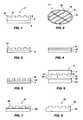
- FIG. 1is a cross-sectional view of a template used in imprint lithography, which is fabricated in accordance with the present invention
- FIG. 2is an elevational view of a template used in imprint lithography, which is fabricated in accordance with the present invention
- FIG. 3schematically illustrates one embodiment of fabricating the template
- FIGS. 4 and 5schematically illustrate another embodiment of fabricating the template.
- FIGS. 6-8schematically illustrate using the template in an imprint lithography process to form features on a semiconductor device
- FIGS. 9-12schematically illustrate another embodiment of fabricating the template.
- a template for use in imprint lithographyincludes a high resolution pattern that may be formed by lithography.
- the pattern on the templateprovides topography that is used to imprint a pattern of corresponding features on a semiconductor device.
- the templatefunctions as a mold or form to transfer the pattern to the semiconductor device, forming the features on a surface thereof contacted by the template.
- the templatemay be transparent to UV wavelength radiation or may be opaque to UV wavelength radiation.
- the features on the semiconductor devicemay have dimensions substantially similar to dimensions of the pattern on the template.
- the featuresmay have a feature size or dimension of less than approximately 100 nm, such as less than approximately 45 nm.
- template 2may include a UV wavelength radiation transparent (which may also be termed “UV transparent” for convenience) layer 4 that has a pattern 6 on its top surface, as shown in FIG. 1 .
- the UV transparent layer 4may be formed from a UV transparent material including, but not limited to, quartz, magnesium fluoride, titanium oxide, calcium fluoride, silicon oxide, silicon dioxide, a polycarbonate material, a PYREX® material, a sapphire material, silicon germanium carbon, gallium nitride, silicon germanium, gallium arsenide, gate oxide, or mixtures or combinations thereof.
- the template 2may be formed from the UV transparent material to allow UV radiation to be transmitted through the template 2 .
- the UV transparent layer 4may be formed from quartz, such as in the form of a quartz wafer. While embodiments herein describe that the UV transparent layer 4 is a quartz layer, other UV transparent materials may also be used.
- the UV transparent layer 4may have substantially the same dimensions (diameter, thickness, etc.) as a conventional semiconductor wafer (silicon wafer) so that processing equipment currently used in photolithography techniques may be used to fabricate the template 2 and so that the template 2 may be used to imprint a pattern on the entire surface of a semiconductor wafer simultaneously. However, if the UV transparent layer 4 has smaller or larger dimensions, the processing equipment may be modified, as desired, to accommodate the UV transparent layer 4 .
- the pattern 6which may also be termed an “imprint pattern” for the sake of convenience, may include a topography having a plurality of recesses 8 and protrusions 10 of satisfactory size, configuration, and orientation in one surface of the UV transparent layer 4 .
- the recesses 8 and protrusions 10 in the template 2are ultimately used to produce substantially identical features on semiconductor devices fabricated on a wafer or other bulk semiconductor substrate contacted by the template.
- an optically opaque material Omay be deposited on the UV transparent layer 4 to form alignment marks 12 , as shown in FIG. 2 .
- the optically opaque material Omay be chromium or chrome, polysilicon, a metal silicide, such as molybdenum silicide, tungsten silicide, or titanium silicide, or a metal, such as aluminum, tungsten, titanium, titanium nitride, tantalum, or tantalum nitride.
- the optically opaque material Omay be deposited by conventional blanket deposition techniques, such as by coating or sputtering techniques.
- the optically opaque material Omay be deposited on portions of the UV transparent layer 4 , such as scribe areas or the periphery, where the alignment marks 12 are desired, the rest of the UV transparent layer 4 being masked to prevent such deposition. Alternatively, as described below, all of template 2 may be covered by opaque material O. To provide proper alignment of the pattern 6 on the V transparent layer 4 , the alignment marks 12 may be formed on the UV transparent layer 4 before forming the pattern 6 . The alignment marks 12 may also be used to align the template 2 with the semiconductor devices, which would typically include semiconductor devices on an unsingulated wafer, onto which the features corresponding to pattern 6 are to be formed.
- a photoresist layer 14may be formed and patterned on the UV transparent layer 4 using a mask (not shown) having opaque and transparent openings in the desired pattern, as shown in FIG. 3 .
- the photoresist layer 14may be formed from a conventional positive or negative photoresist material and may be deposited by conventional techniques, such as by spin coating.
- the opaque and transparent openings in the maskform a pattern that is complementary to the pattern 6 that is ultimately to be formed on the template 2 .
- the maskmay be fabricated by conventional techniques and, therefore, is not described in detail herein.
- the maskmay include, for example, a 4 ⁇ pattern in that the pattern is four times the size of the pattern 6 formed on the template 2 and four times the size of the features ultimately formed on the semiconductor device.
- the photoresist layer 14may be exposed and developed, as known in the art, exposing selected portions of the UV transparent layer 4 to electromagnetic radiation. Exposure and development of the photoresist layer 14 may be performed using conventional exposure equipment and developing solutions. Developing solutions for the photoresist layer 14 may be selected by one of ordinary skill in the art and, therefore, are not discussed in detail herein. In addition to conventional photolithography, electron beam projection, electron beam direct write, ion direct write, or maskless lithography may be used to form the pattern 6 on the template 2 .
- the pattern in the photoresist layer 14may be then transferred to the UV transparent layer 4 and the alignment marks 12 formed in the opaque material O by etching, producing the template 2 shown in FIG. 1 .
- Two separate, selective etchesmay also be used, one for opaque material O and one for UV transparent layer 4 .
- the UV transparent layer 4may be etched isotropically (wet etched) or anisotropically (dry etched). Wet and dry etching solutions for the UV transparent materials described above are known in the art and, therefore, are not discussed in detail herein.
- the UV transparent layer 4may desirably be anisotropically etched.
- the quartzmay be etched using a fluorine-based plasma etch.
- the fluorine-based plasmamay include a fluorine-containing gas, such as CF 4 , CHF 3 , C 4 F 8 , SF 6 , or mixtures thereof, and an inert gas, such as argon, xenon, or mixtures thereof.
- the UV transparent layer 4may be patterned as illustrated in FIGS. 4 and 5 to produce the template 2 .
- a chromium layer 16used as optically opaque material O, may be blanket deposited over the UV transparent layer 4 and the photoresist layer 14 deposited over the chromium layer 16 , as shown in FIG. 4 .
- the chromium layer 16may be deposited by conventional techniques and may range in thickness from approximately 80 nm to approximately 100 nm. While layer 16 is described as being formed from chromium, layer 16 may be formed from other metal materials that are opaque to the imaging wavelength and have significant etch selectivity relative to the UV transparent layer 4 including, but not limited to, chromium oxide, titanium, titanium nitride, tungsten, or mixtures thereof.
- the photoresist layer 14may be a conventional photoresist material and may be deposited by conventional techniques, such as spin coating.
- the photoresist layer 14may be patterned as described above, to expose portions of the chromium layer 16 .
- the pattern in the photoresist layer 14may be transferred to the chromium layer 16 and, subsequently, to the UV transparent layer 4 , by etching.
- the exposed portions of the chromium layer 16may be etched, using the photoresist layer 14 as a mask.
- the remaining portions of the chromium layer 16may function as a hard mask for etching the UV transparent layer 4 and to provide alignment marks 12 .
- Each of the chromium layer 16 and the UV transparent layer 4may be etched using a suitable, conventional wet or dry etch process.
- the etching solutionsmay be selected by one of ordinary skill in the art and, therefore, are not discussed in detail herein.
- the UV transparent layer 4may be etched anisotropically, such as by using the fluorine-based plasma etch described above. Any portions of the photoresist layer 14 and undesired portions of the chromium layer 16 remaining on the UV transparent layer 4 after etching may be removed as desired, producing the pattern 6 and alignment marks 12 on the template 2 , as shown in FIGS. 1 and 2 .
- the thickness of the UV transparent layer 4may be insufficient to provide adequate mechanical strength during handling and use of the template 2 when it is used in imprint lithography. Therefore, the template 2 may optionally be bonded to a second UV transparent material substrate 5 as shown in broken lines in FIG. 1 to provide additional mechanical integrity.
- the second UV transparent material substrate 5may be one or more of the materials described above for use as the UV transparent layer 4 .
- the template 2 and the second UV transparent material substrate 5may be adhered with an adhesive composition that does not affect the UV transparency of the template 2 . In other words, the template 2 and the second UV transparent material substrate 5 , when bonded, may remain UV transparent. It would also be desirable, for alignment and pattern resolution purposes, for the template 2 , including second UV transparent material substrate 5 and any bonding materials, to exhibit a substantially uniform index of refraction through the thickness thereof.
- the template 2 shown in FIGS. 1 and 2may be used directly in an imprint lithographic technique to imprint the pattern 6 on a semiconductor wafer or other bulk semiconductor substrate of like size bearing a plurality of semiconductor devices, forming corresponding features on the semiconductor devices.
- the features to be formed on the semiconductor devicesmay be a negative image (reversed image) of the pattern 6 on the template 2 .
- the template 2may be divided, such as by dicing, to form smaller templates that are used in imprint lithography or smaller groups of semiconductor devices.
- the pattern 6 on each of the smaller templatesmay be the same or different.
- the template 2 on each of the divided templatesmay be bonded to the optional second UV transparent material substrate 5 before or after dicing.
- semiconductor device 18may include a bare substrate 20 and additional layers thereon, such as metal layers, oxide layers, carbon hard mask layers, or polysilicon layers.
- the semiconductor device 18may also include trenches or diffusion regions. For the sake of clarity, the additional layers, trenches, and diffusion regions are not shown in FIG. 6 .
- the bare substrate 20may be a conventional substrate or other bulk substrate having a layer of semiconductor material.
- the term “bulk substrate”includes not only silicon wafers, but also silicon on insulator (“SOI”) substrates, silicon on sapphire (“SOS”) substrates, epitaxial layers of silicon on a base semiconductor foundation, and other semiconductor, optoelectronics, or biotechnology materials, such as silicon-germanium, germanium, gallium arsenide, or indium phosphide.
- the semiconductor device 18may also include a transfer layer 22 that is deformable under pressure and does not adhere to a surface of the template 2 , especially as the template 2 is removed from the semiconductor device 18 . Since the transfer layer 22 is deformable, the transfer layer 22 may fill the recesses 8 in the pattern 6 when the template 2 and the semiconductor device 18 come into contact.
- the transfer layer 22may be a radiation sensitive material including, but not limited to, a photocurable or photosensitive material, such as a photoresist material.
- the transfer layer 22may be sensitive to UV light, visible light, infrared light, actinic light, or other radiation sources, such as electron beams or x-rays. Materials that may be used as the transfer layer 22 are known in the art. For the sake of example only, the transfer layer 22 may be formed from a conventional photoresist material that is curable by exposure to UV light, such as a curable organosilicon material.
- the semiconductor device 18 and the template 2may be maintained substantially parallel, and in close proximity, to one another.
- the semiconductor device 18 and the template 2may then be contacted with minimal pressure so that the transfer layer 22 deforms into the pattern 6 of the template 2 .
- the semiconductor device 18may thus be provided with a negative image 24 (reversed image) of the pattern 6 in its imprinted transfer layer 22 . If the transfer layer 22 is a radiation-sensitive material, the transfer layer 22 may subsequently be exposed to radiation, such as UV radiation.
- the UV radiationis transmitted through the template 2 from the back, unpatterned surface thereof to harden portions of the negative image 24 of transfer layer 22 that include photoresist material filling recesses 8 of pattern 6 or to harden all of the negative image 24 of transfer layer 22 that includes photoresist material filling recesses 8 and protrusions 10 of pattern 6 .
- the transfer layer 22includes a material that is sensitive to heat, pressure, or combinations thereof, which are generated by contacting the template 2 with the semiconductor device 18 , the heat, pressure, or combinations thereof may be used to cure, harden, or solidify the transfer layer 22 .
- the template 2may then be removed from the semiconductor device 18 .
- the template 2 and the semiconductor device 18may be separated without damaging, or otherwise adversely affecting, the negative image 24 .
- the template 2may be treated with a material that lowers the surface energy of the template 2 , as known in the art, to assist in separating the template 2 from the semiconductor wafer or other bulk substrate 18 without damage to the imprinted, exposed negative image 24 .
- the negative image 24 in the transfer layer 22may be transferred to the substrate 20 or underlying layers of the semiconductor device 18 using the transfer layer 22 as a mask.
- the negative image 24may be transferred into the substrate 20 or into the metal, carbon, hard mask layer, oxide, or polysilicon layers previously formed on the substrate 20 by dry etching or wet etching. Any remaining portions of the transfer layer 22 may then be removed, providing the features 26 on the semiconductor device 18 as shown in FIG. 8 .
- the features 26may be substantially the same size, configuration, and orientation as the dimensions of the pattern 6 on the template 2 . Since the pattern 6 is formed by photolithography, the feature sizes may be determined by the resolution of the photolithographic techniques used to form the pattern 6 .
- the features 26have a feature size of less than approximately 100 nm, such as less than approximately 45 nm.
- the negative image 24 in the transfer layer 22may be subjected to ion implantation to form implanted regions on the semiconductor device.
- the template 2may be used as a master template to create at least one daughter template.
- the pattern 6 on the template 2may be transferred to an additional structure, which includes a UV transparent material and a transfer layer, such as a photoresist layer.
- the UV transparent material and transfer layer of the structure that is ultimately to become the daughter templatemay be one of the materials described above.
- the transfer layermay be deformable under pressure so that when the template 2 contacts the transfer layer of the structure that is ultimately to be the daughter template, the pattern 6 of the master template is transferred to the transfer layer.
- the pattern in the transfer layermay subsequently be etched into the UV transparent material, producing the daughter template.
- the pattern on each of the daughter templatesmay be the reverse of the pattern 6 on the master template. In other words, the pattern 6 on the master template may be a negative image of the pattern on the daughter template.
- the template 2Since the template 2 contacts the semiconductor device 18 during imprint lithography, the template 2 may become easily damaged. Therefore, the master template may be stored and preserved while one of the daughter templates fabricated from it is used to imprint the features on the semiconductor devices. If the daughter template is damaged during imprinting, another daughter template may be used to imprint the features or the master template may be used to create additional daughter templates.
- the template 2 ′may include more than one UV transparent layer (see FIG. 12 ), where at least one of the UV transparent layers has a pattern on an exposed surface thereof.
- the template 2 ′may be formed using a layer of material that is opaque to UV radiation, which is removed before using the template 2 ′ in imprint lithography.
- the UV wavelength radiation opaque (also termed merely “UV opaque” for the sake of convenience) layer 28may be formed from silicon, such as a silicon wafer, ceramic, or a metal material. As shown in FIG. 9 , the UV opaque layer 28 may be etched to include a first pattern 30 , which is a negative image of a second pattern 40 (see FIG. 12 ) that is ultimately formed on the surface of template 2 ′.
- the first pattern 30may include recesses 32 and protrusions 34 .
- the UV opaque layer 28may be patterned using conventional photolithographic techniques.
- a mask(not shown) having opaque and transparent portions may be used.
- the opaque and transparent portionsform a pattern in the mask, which is used to produce the first pattern 30 on a photoresist layer covering the UV opaque layer 28 .
- the maskmay be fabricated by conventional techniques and may be used in patterning the UV opaque layer 28 as previously discussed.
- the photoresist on UV opaque layer 28may be developed and the UV opaque layer 28 etched using conventional developing solutions and etch solutions or dry etch chemistries. Alignment marks (not shown) may also be patterned and etched into the UV opaque layer 28 by conventional techniques.
- a UV transparent materialmay be deposited over the UV opaque layer 28 , filling in the recesses 32 of the first pattern 30 and forming a first UV transparent layer 36 .
- the UV transparent materialis silicon dioxide.
- other UV transparent materialsmay also be used, such as those described earlier.
- the upper surface of the first UV transparent layer 36is substantially planar.
- First UV transparent layer 36may be deposited using a highly conformal deposition technique including, but not limited to, chemical vapor deposition (“CVD”), physical vapor deposition (“PVD”), atomic layer deposition (“ALD”), spin coating, or combinations thereof.
- the UV transparent materialis deposited conformally so that the recesses 32 in the first pattern 30 may be filled without forming voids between the first UV transparent layer 36 and the topography of UV opaque layer 28 . If the UV opaque layer 28 includes a large recess, the first UV transparent layer 36 may be formed by filling this recess with the UV transparent material using a combination of ALD to conform to the topography of opaque layer 28 , followed by spin coating.
- the first UV transparent layer 36may be bonded to a second UV transparent layer 38 , as shown in FIG. 11 , sandwiching the first UV transparent layer 36 between the UV opaque layer 28 and the second UV transparent layer 38 .
- the second UV transparent layer 38may be one of the UV transparent materials described earlier.
- the second UV transparent layer 38may be a quartz wafer. Since the surface of the first UV transparent layer 36 not in contact with UV opaque layer 28 is substantially planar, good adhesion may be obtained between the first UV transparent layer 36 and the second UV transparent layer 38 .
- the two UV transparent layersmay be bonded using an adhesive composition that does not affect the UV transparency of either of these layers. Such adhesive compositions are known in the art and may be selected by one of ordinary skill in the art. As with the previous embodiment, it is desirable that a substantially uniform index of refraction be maintained throughout the thickness of template 2 ′.
- the template 2 ′may be used in SOI wafer bonding techniques.
- the UV opaque layer 28may be removed from the first UV transparent layer 36 , forming a template 2 ′ that includes the first and second UV transparent layers 36 , 38 .
- the template 2 ′is as shown in FIG. 12 and includes the second pattern 40 in the first UV transparent layer 36 .
- the UV opaque layer 28may be removed using conventional wet or dry etch techniques selective for the UV opaque layer 28 relative to the first and second UV transparent layers 36 , 38 . As such, the first UV transparent layer 36 and the second UV transparent layer 38 may remain substantially undamaged after removing the UV opaque layer 28 .
- the UV opaque layer 28is etched using a conventional wet etch, which is inexpensive and rapid. Portions of UV opaque layer 28 may be left unetched (as by selective masking) to define alignment marks 12 (see FIG. 2 ).
- the second pattern 40 on the template 2 ′may be transferred to a semiconductor device by imprint lithography, forming features on the semiconductor device.
- the featuresmay be a negative image (reversed image) of the second pattern 40 , which is itself a negative image of the first pattern 30 formed in the UV opaque layer 28 .
- the semiconductor devicemay be imprinted with the template 2 ′, substantially as described above in regard to FIGS. 6-8 , except that template 2 ′ is used instead of template 2 .
- the templatemay include a UV opaque layer having a pattern on its top surface.
- the techniques described abovemay be used to form the UV opaque template, except that a UV opaque material is used instead of a UV transparent material.
- the UV opaque template of this embodimentis substantially as shown in FIG. 1 , except that the UV opaque template includes a UV opaque material.
- the UV opaque materialmay be silicon, a ceramic, or a metal material.
- the UV opaque materialmay be etched to include the pattern, which is a negative image of the pattern that is ultimately formed on the semiconductor device 18 .
- the patternmay include recesses and protrusions, which are formed using conventional photolithographic techniques.
- the recesses and protrusions in the UV opaque templateare ultimately used to produce substantially identical features on the semiconductor device 18 .
- Alignment marks(not shown) may also be patterned and etched into the UV opaque material by conventional techniques.
- the UV opaque templatemay optionally be bonded to a second UV opaque material substrate, as previously described, to provide additional mechanical integrity.
- the UV opaque templatemay be brought into contact with the transfer layer 22 of the semiconductor device 18 .
- the transfer layer 22may fill the recesses in the pattern on the UV opaque template, transferring a negative image 24 (reversed image) of the pattern to the transfer layer 22 of the semiconductor device 18 .
- the transfer layer 22may be a material that is cured or hardened by heat, pressure, or combinations thereof. Such materials are known in the art and, therefore, are not described in detail herein.
- the heat, pressure, or combinations thereof used to cure, harden, or solidify the transfer layer 22may be generated upon contact between the UV opaque template and the semiconductor device 18 .
- the UV opaque templatemay then be removed from the semiconductor device 18 , as previously described, without damaging, or otherwise adversely affecting, the negative image 24 .
- the negative image 24 in the transfer layer 22may be transferred to the substrate 20 or underlying layers of the semiconductor device 18 using the transfer layer 22 as a mask.
- the negative image 24may be transferred into the substrate 20 or into the metal, carbon, hard mask layer, oxide, or polysilicon layers previously formed on the substrate 20 by dry etching or wet etching. Any remaining portions of the transfer layer 22 may then be removed, providing the features 26 on the semiconductor device 18 .
- the features 26may be substantially the same size, configuration, and orientation as the dimensions of the pattern on the UV opaque template. Since the pattern is formed by photolithography, the feature sizes may be determined by the resolution of the photolithographic techniques used to form the pattern.
- the features 26have a feature size of less than approximately 100 nm, such as less than approximately 45 nm.
- the negative image 24 in the transfer layer 22may be subjected to ion implantation to form implanted regions on the semiconductor device.
- the UV transparent or UV opaque templates produced by the methods of the present inventionprovide numerous advantages. In forming the semiconductor device 18 , if imprint lithography is used at some process levels and conventional photolithography is used at other process levels, lens distortion and magnification factor effects are typically observed in the semiconductor device 18 . However, the UV transparent or UV opaque templates formed by the methods of the present invention may be used to provide improved matching between the imprint lithography process levels and the conventional photolithography process levels. For instance, if the same photostepper used in the process levels formed by conventional photolithography is also used to form the UV transparent template or the UV opaque template, the lens distortion and magnification factor effects at the different process levels in the semiconductor device 18 may be minimized. The method of the present invention may also provide the UV transparent template or the UV opaque template at a reduced cost compared to conventional techniques.
Landscapes
- Engineering & Computer Science (AREA)
- Chemical & Material Sciences (AREA)
- Physics & Mathematics (AREA)
- Nanotechnology (AREA)
- General Physics & Mathematics (AREA)
- Crystallography & Structural Chemistry (AREA)
- Theoretical Computer Science (AREA)
- Mathematical Physics (AREA)
- Condensed Matter Physics & Semiconductors (AREA)
- Manufacturing & Machinery (AREA)
- Health & Medical Sciences (AREA)
- Toxicology (AREA)
- Exposure Of Semiconductors, Excluding Electron Or Ion Beam Exposure (AREA)
- Shaping Of Tube Ends By Bending Or Straightening (AREA)
- Moulds For Moulding Plastics Or The Like (AREA)
Abstract
Description
Claims (24)
Priority Applications (3)
| Application Number | Priority Date | Filing Date | Title |
|---|---|---|---|
| US11/155,167US7771917B2 (en) | 2005-06-17 | 2005-06-17 | Methods of making templates for use in imprint lithography |
| US12/839,755US8657597B2 (en) | 2005-06-17 | 2010-07-20 | Templates for use in imprint lithography and related intermediate template structures |
| US14/168,650US20140147542A1 (en) | 2005-06-17 | 2014-01-30 | Template structures including ultraviolet wavelength radiation transparent material |
Applications Claiming Priority (1)
| Application Number | Priority Date | Filing Date | Title |
|---|---|---|---|
| US11/155,167US7771917B2 (en) | 2005-06-17 | 2005-06-17 | Methods of making templates for use in imprint lithography |
Related Child Applications (1)
| Application Number | Title | Priority Date | Filing Date |
|---|---|---|---|
| US12/839,755DivisionUS8657597B2 (en) | 2005-06-17 | 2010-07-20 | Templates for use in imprint lithography and related intermediate template structures |
Publications (2)
| Publication Number | Publication Date |
|---|---|
| US20060286490A1 US20060286490A1 (en) | 2006-12-21 |
| US7771917B2true US7771917B2 (en) | 2010-08-10 |
Family
ID=37573777
Family Applications (3)
| Application Number | Title | Priority Date | Filing Date |
|---|---|---|---|
| US11/155,167Active2028-07-06US7771917B2 (en) | 2005-06-17 | 2005-06-17 | Methods of making templates for use in imprint lithography |
| US12/839,755Active2025-10-27US8657597B2 (en) | 2005-06-17 | 2010-07-20 | Templates for use in imprint lithography and related intermediate template structures |
| US14/168,650AbandonedUS20140147542A1 (en) | 2005-06-17 | 2014-01-30 | Template structures including ultraviolet wavelength radiation transparent material |
Family Applications After (2)
| Application Number | Title | Priority Date | Filing Date |
|---|---|---|---|
| US12/839,755Active2025-10-27US8657597B2 (en) | 2005-06-17 | 2010-07-20 | Templates for use in imprint lithography and related intermediate template structures |
| US14/168,650AbandonedUS20140147542A1 (en) | 2005-06-17 | 2014-01-30 | Template structures including ultraviolet wavelength radiation transparent material |
Country Status (1)
| Country | Link |
|---|---|
| US (3) | US7771917B2 (en) |
Cited By (2)
| Publication number | Priority date | Publication date | Assignee | Title |
|---|---|---|---|---|
| US20170018680A1 (en)* | 2015-07-13 | 2017-01-19 | Sensor Electronic Technology, Inc. | P-type Contact to Semiconductor Heterostructure |
| US10236415B2 (en) | 2015-07-13 | 2019-03-19 | Sensor Electronic Technology, Inc. | P-type contact to semiconductor heterostructure |
Families Citing this family (41)
| Publication number | Priority date | Publication date | Assignee | Title |
|---|---|---|---|---|
| US7771917B2 (en)* | 2005-06-17 | 2010-08-10 | Micron Technology, Inc. | Methods of making templates for use in imprint lithography |
| US7998651B2 (en)* | 2006-05-15 | 2011-08-16 | Asml Netherlands B.V. | Imprint lithography |
| US7968253B2 (en)* | 2006-06-20 | 2011-06-28 | Samsung Electronics Co., Ltd. | Nano imprint master and method of manufacturing the same |
| US8394483B2 (en) | 2007-01-24 | 2013-03-12 | Micron Technology, Inc. | Two-dimensional arrays of holes with sub-lithographic diameters formed by block copolymer self-assembly |
| US8083953B2 (en) | 2007-03-06 | 2011-12-27 | Micron Technology, Inc. | Registered structure formation via the application of directed thermal energy to diblock copolymer films |
| US8557128B2 (en) | 2007-03-22 | 2013-10-15 | Micron Technology, Inc. | Sub-10 nm line features via rapid graphoepitaxial self-assembly of amphiphilic monolayers |
| US7959975B2 (en) | 2007-04-18 | 2011-06-14 | Micron Technology, Inc. | Methods of patterning a substrate |
| US8097175B2 (en) | 2008-10-28 | 2012-01-17 | Micron Technology, Inc. | Method for selectively permeating a self-assembled block copolymer, method for forming metal oxide structures, method for forming a metal oxide pattern, and method for patterning a semiconductor structure |
| US8294139B2 (en) | 2007-06-21 | 2012-10-23 | Micron Technology, Inc. | Multilayer antireflection coatings, structures and devices including the same and methods of making the same |
| US8372295B2 (en) | 2007-04-20 | 2013-02-12 | Micron Technology, Inc. | Extensions of self-assembled structures to increased dimensions via a “bootstrap” self-templating method |
| US7833695B2 (en)* | 2007-05-31 | 2010-11-16 | Corning Incorporated | Methods of fabricating metal contact structures for laser diodes using backside UV exposure |
| US8404124B2 (en) | 2007-06-12 | 2013-03-26 | Micron Technology, Inc. | Alternating self-assembling morphologies of diblock copolymers controlled by variations in surfaces |
| US8080615B2 (en) | 2007-06-19 | 2011-12-20 | Micron Technology, Inc. | Crosslinkable graft polymer non-preferentially wetted by polystyrene and polyethylene oxide |
| JP5002422B2 (en)* | 2007-11-14 | 2012-08-15 | 株式会社日立ハイテクノロジーズ | Resin stamper for nanoprint |
| US8999492B2 (en) | 2008-02-05 | 2015-04-07 | Micron Technology, Inc. | Method to produce nanometer-sized features with directed assembly of block copolymers |
| US8101261B2 (en) | 2008-02-13 | 2012-01-24 | Micron Technology, Inc. | One-dimensional arrays of block copolymer cylinders and applications thereof |
| US8426313B2 (en) | 2008-03-21 | 2013-04-23 | Micron Technology, Inc. | Thermal anneal of block copolymer films with top interface constrained to wet both blocks with equal preference |
| US8425982B2 (en) | 2008-03-21 | 2013-04-23 | Micron Technology, Inc. | Methods of improving long range order in self-assembly of block copolymer films with ionic liquids |
| US20090263729A1 (en)* | 2008-04-21 | 2009-10-22 | Micron Technology, Inc. | Templates for imprint lithography and methods of fabricating and using such templates |
| US8114300B2 (en) | 2008-04-21 | 2012-02-14 | Micron Technology, Inc. | Multi-layer method for formation of registered arrays of cylindrical pores in polymer films |
| US8114301B2 (en) | 2008-05-02 | 2012-02-14 | Micron Technology, Inc. | Graphoepitaxial self-assembly of arrays of downward facing half-cylinders |
| JP4922376B2 (en)* | 2009-09-18 | 2012-04-25 | 株式会社東芝 | Template manufacturing method and semiconductor device manufacturing method |
| JP5491997B2 (en)* | 2010-07-07 | 2014-05-14 | 株式会社東芝 | Template manufacturing method and semiconductor device manufacturing method |
| US8304493B2 (en) | 2010-08-20 | 2012-11-06 | Micron Technology, Inc. | Methods of forming block copolymers |
| DE102011010895B4 (en)* | 2011-02-10 | 2022-04-28 | OSRAM Opto Semiconductors Gesellschaft mit beschränkter Haftung | Light-emitting diode module and method for operating a light-emitting diode module |
| US8967992B2 (en)* | 2011-04-25 | 2015-03-03 | Canon Nanotechnologies, Inc. | Optically absorptive material for alignment marks |
| JP2013004669A (en)* | 2011-06-15 | 2013-01-07 | Toshiba Corp | Pattern formation method, electronic device manufacturing method and electronic device |
| CN103091747B (en)* | 2011-10-28 | 2015-11-25 | 清华大学 | A kind of preparation method of grating |
| US8900963B2 (en) | 2011-11-02 | 2014-12-02 | Micron Technology, Inc. | Methods of forming semiconductor device structures, and related structures |
| US9082914B2 (en)* | 2012-01-13 | 2015-07-14 | Gaurdian Industries Corp. | Photovoltaic module including high contact angle coating on one or more outer surfaces thereof, and/or methods of making the same |
| US9087699B2 (en) | 2012-10-05 | 2015-07-21 | Micron Technology, Inc. | Methods of forming an array of openings in a substrate, and related methods of forming a semiconductor device structure |
| KR20140076357A (en)* | 2012-12-12 | 2014-06-20 | 삼성전자주식회사 | Nanoimprint stamp having high contrast alignment mark and method of fabricating the same |
| JP2014120526A (en)* | 2012-12-13 | 2014-06-30 | Toshiba Corp | Pattern formation method and method for manufacturing template for imprinting |
| US9229328B2 (en) | 2013-05-02 | 2016-01-05 | Micron Technology, Inc. | Methods of forming semiconductor device structures, and related semiconductor device structures |
| US9177795B2 (en) | 2013-09-27 | 2015-11-03 | Micron Technology, Inc. | Methods of forming nanostructures including metal oxides |
| US20160257117A1 (en)* | 2013-10-28 | 2016-09-08 | Hewlett-Packard Development Company, L.P. | Encapsulating a Bonded Wire with Low Profile Encapsulation |
| US9406499B2 (en)* | 2014-02-12 | 2016-08-02 | Taiwan Semiconductor Manufacturing Company Ltd. | Semiconductor wafer structure |
| EP3400193B1 (en)* | 2016-01-04 | 2020-10-21 | King Abdullah University Of Science And Technology | Nanoneedles for intracellular applications |
| DE102016110523B4 (en)* | 2016-06-08 | 2023-04-06 | Infineon Technologies Ag | Processing a power semiconductor device |
| CN109983392B (en)* | 2016-12-09 | 2021-02-23 | 应用材料公司 | Collimated LED light field display |
| WO2024097362A1 (en)* | 2022-11-04 | 2024-05-10 | Arizona Board Of Regents On Behalf Of The University Of Arizona | Infrared plastic optics from chalcogenide hybrid inorganic/organic polymers |
Citations (15)
| Publication number | Priority date | Publication date | Assignee | Title |
|---|---|---|---|---|
| US5817242A (en)* | 1995-08-04 | 1998-10-06 | International Business Machines Corporation | Stamp for a lithographic process |
| US6120697A (en)* | 1997-12-31 | 2000-09-19 | Alliedsignal Inc | Method of etching using hydrofluorocarbon compounds |
| US6517977B2 (en) | 2001-03-28 | 2003-02-11 | Motorola, Inc. | Lithographic template and method of formation and use |
| US6580172B2 (en) | 2001-03-02 | 2003-06-17 | Motorola, Inc. | Lithographic template and method of formation and use |
| US20030203319A1 (en)* | 2002-04-23 | 2003-10-30 | Heon Lee | Method of fabricating sub-lithographic sized line and space patterns for nano-imprinting lithography |
| US20030205657A1 (en) | 2002-05-01 | 2003-11-06 | Voisin Ronald D. | Methods of manufacturing a lithography template |
| US20040008334A1 (en) | 2002-07-11 | 2004-01-15 | Sreenivasan Sidlgata V. | Step and repeat imprint lithography systems |
| US6716754B2 (en) | 2002-03-12 | 2004-04-06 | Micron Technology, Inc. | Methods of forming patterns and molds for semiconductor constructions |
| US6842229B2 (en) | 2000-07-16 | 2005-01-11 | Board Of Regents, The University Of Texas System | Imprint lithography template comprising alignment marks |
| US20050031998A1 (en)* | 2003-08-08 | 2005-02-10 | Ga-Lane Chen | Method for manufacturing light guide plate stamper |
| US20050064344A1 (en)* | 2003-09-18 | 2005-03-24 | University Of Texas System Board Of Regents | Imprint lithography templates having alignment marks |
| US20050230882A1 (en) | 2004-04-19 | 2005-10-20 | Molecular Imprints, Inc. | Method of forming a deep-featured template employed in imprint lithography |
| JP2007245702A (en) | 2006-02-20 | 2007-09-27 | Asahi Glass Co Ltd | Template and method for producing treated substrate having transferred fine pattern |
| KR20080033676A (en) | 2006-10-13 | 2008-04-17 | 주식회사 동진쎄미켐 | Resin mold for imprint lithography and manufacturing method thereof |
| US20080230947A1 (en)* | 1995-11-15 | 2008-09-25 | Princeton University | Articles Comprising Nanoscale Patterns With Reduced Edge Roughness and Methods of Making Same |
Family Cites Families (10)
| Publication number | Priority date | Publication date | Assignee | Title |
|---|---|---|---|---|
| DE69325692T2 (en) | 1992-08-18 | 2000-01-05 | The Spectranetics Corp., Colorado Springs | Guide wire with fiber optics |
| JP2947196B2 (en)* | 1997-01-23 | 1999-09-13 | 日本電気株式会社 | Semiconductor substrate and method of manufacturing semiconductor device |
| JP2002214414A (en)* | 2001-01-22 | 2002-07-31 | Omron Corp | Optical element with thin resin film having micro-rugged pattern, method for producing the same and apparatus therefor |
| US7063919B2 (en)* | 2002-07-31 | 2006-06-20 | Mancini David P | Lithographic template having a repaired gap defect method of repair and use |
| US6916584B2 (en)* | 2002-08-01 | 2005-07-12 | Molecular Imprints, Inc. | Alignment methods for imprint lithography |
| US7083880B2 (en)* | 2002-08-15 | 2006-08-01 | Freescale Semiconductor, Inc. | Lithographic template and method of formation and use |
| US7136150B2 (en)* | 2003-09-25 | 2006-11-14 | Molecular Imprints, Inc. | Imprint lithography template having opaque alignment marks |
| US7140861B2 (en)* | 2004-04-27 | 2006-11-28 | Molecular Imprints, Inc. | Compliant hard template for UV imprinting |
| US7771917B2 (en) | 2005-06-17 | 2010-08-10 | Micron Technology, Inc. | Methods of making templates for use in imprint lithography |
| US20090263729A1 (en) | 2008-04-21 | 2009-10-22 | Micron Technology, Inc. | Templates for imprint lithography and methods of fabricating and using such templates |
- 2005
- 2005-06-17USUS11/155,167patent/US7771917B2/enactiveActive
- 2010
- 2010-07-20USUS12/839,755patent/US8657597B2/enactiveActive
- 2014
- 2014-01-30USUS14/168,650patent/US20140147542A1/ennot_activeAbandoned
Patent Citations (16)
| Publication number | Priority date | Publication date | Assignee | Title |
|---|---|---|---|---|
| US5817242A (en)* | 1995-08-04 | 1998-10-06 | International Business Machines Corporation | Stamp for a lithographic process |
| US20080230947A1 (en)* | 1995-11-15 | 2008-09-25 | Princeton University | Articles Comprising Nanoscale Patterns With Reduced Edge Roughness and Methods of Making Same |
| US6120697A (en)* | 1997-12-31 | 2000-09-19 | Alliedsignal Inc | Method of etching using hydrofluorocarbon compounds |
| US6842229B2 (en) | 2000-07-16 | 2005-01-11 | Board Of Regents, The University Of Texas System | Imprint lithography template comprising alignment marks |
| US6580172B2 (en) | 2001-03-02 | 2003-06-17 | Motorola, Inc. | Lithographic template and method of formation and use |
| US6517977B2 (en) | 2001-03-28 | 2003-02-11 | Motorola, Inc. | Lithographic template and method of formation and use |
| US6716754B2 (en) | 2002-03-12 | 2004-04-06 | Micron Technology, Inc. | Methods of forming patterns and molds for semiconductor constructions |
| US6759180B2 (en) | 2002-04-23 | 2004-07-06 | Hewlett-Packard Development Company, L.P. | Method of fabricating sub-lithographic sized line and space patterns for nano-imprinting lithography |
| US20030203319A1 (en)* | 2002-04-23 | 2003-10-30 | Heon Lee | Method of fabricating sub-lithographic sized line and space patterns for nano-imprinting lithography |
| US20030205657A1 (en) | 2002-05-01 | 2003-11-06 | Voisin Ronald D. | Methods of manufacturing a lithography template |
| US20040008334A1 (en) | 2002-07-11 | 2004-01-15 | Sreenivasan Sidlgata V. | Step and repeat imprint lithography systems |
| US20050031998A1 (en)* | 2003-08-08 | 2005-02-10 | Ga-Lane Chen | Method for manufacturing light guide plate stamper |
| US20050064344A1 (en)* | 2003-09-18 | 2005-03-24 | University Of Texas System Board Of Regents | Imprint lithography templates having alignment marks |
| US20050230882A1 (en) | 2004-04-19 | 2005-10-20 | Molecular Imprints, Inc. | Method of forming a deep-featured template employed in imprint lithography |
| JP2007245702A (en) | 2006-02-20 | 2007-09-27 | Asahi Glass Co Ltd | Template and method for producing treated substrate having transferred fine pattern |
| KR20080033676A (en) | 2006-10-13 | 2008-04-17 | 주식회사 동진쎄미켐 | Resin mold for imprint lithography and manufacturing method thereof |
Non-Patent Citations (3)
| Title |
|---|
| International Search Report for PCT/US2009/038914, dated Oct. 29, 2009, three (3) pages. |
| Nishant Sinha, U.S. Appl. No. 12/106,732, filed Apr. 21, 2008. |
| Written Opinion of the International Searching Authority for PCT/US2009/038914, dated Oct. 29, 2009, four (4) pages. |
Cited By (3)
| Publication number | Priority date | Publication date | Assignee | Title |
|---|---|---|---|---|
| US20170018680A1 (en)* | 2015-07-13 | 2017-01-19 | Sensor Electronic Technology, Inc. | P-type Contact to Semiconductor Heterostructure |
| US9859461B2 (en)* | 2015-07-13 | 2018-01-02 | Sensor Electronic Technology, Inc. | P-type contact to semiconductor heterostructure |
| US10236415B2 (en) | 2015-07-13 | 2019-03-19 | Sensor Electronic Technology, Inc. | P-type contact to semiconductor heterostructure |
Also Published As
| Publication number | Publication date |
|---|---|
| US20100285167A1 (en) | 2010-11-11 |
| US8657597B2 (en) | 2014-02-25 |
| US20140147542A1 (en) | 2014-05-29 |
| US20060286490A1 (en) | 2006-12-21 |
Similar Documents
| Publication | Publication Date | Title |
|---|---|---|
| US7771917B2 (en) | Methods of making templates for use in imprint lithography | |
| CN1960855B (en) | Flexible rigid stencil for UV marking | |
| US6890688B2 (en) | Lithographic template and method of formation and use | |
| US6852454B2 (en) | Multi-tiered lithographic template and method of formation and use | |
| US6517977B2 (en) | Lithographic template and method of formation and use | |
| US6580172B2 (en) | Lithographic template and method of formation and use | |
| JP5563544B2 (en) | Method for forming a recess in a surface | |
| US7922960B2 (en) | Fine resist pattern forming method and nanoimprint mold structure | |
| EP1072954A2 (en) | Lithographic process for device fabrication | |
| EP1795958A1 (en) | Method of fabricating nanoimprint mold | |
| KR100943402B1 (en) | Method of forming and repairing a lithographic template having a gap defect | |
| US7163888B2 (en) | Direct imprinting of etch barriers using step and flash imprint lithography | |
| US20090263729A1 (en) | Templates for imprint lithography and methods of fabricating and using such templates | |
| US7041436B2 (en) | Method for the manufacture of micro structures | |
| US20050074697A1 (en) | Method for fabricating masters for imprint lithography and related imprint process | |
| CN1996141A (en) | Impression die with zero film thickness and impression-photoetched pattern transferring method | |
| JPH04127515A (en) | X-ray mask inspecting method |
Legal Events
| Date | Code | Title | Description |
|---|---|---|---|
| AS | Assignment | Owner name:MICRON TECHNOLOGY, INC., IDAHO Free format text:ASSIGNMENT OF ASSIGNORS INTEREST;ASSIGNORS:SANDHU, GURTEJ S.;RERICHA, WILLIAM T.;REEL/FRAME:016708/0123 Effective date:20050610 | |
| FEPP | Fee payment procedure | Free format text:PAYOR NUMBER ASSIGNED (ORIGINAL EVENT CODE: ASPN); ENTITY STATUS OF PATENT OWNER: LARGE ENTITY | |
| STCF | Information on status: patent grant | Free format text:PATENTED CASE | |
| FPAY | Fee payment | Year of fee payment:4 | |
| AS | Assignment | Owner name:U.S. BANK NATIONAL ASSOCIATION, AS COLLATERAL AGENT, CALIFORNIA Free format text:SECURITY INTEREST;ASSIGNOR:MICRON TECHNOLOGY, INC.;REEL/FRAME:038669/0001 Effective date:20160426 Owner name:U.S. BANK NATIONAL ASSOCIATION, AS COLLATERAL AGEN Free format text:SECURITY INTEREST;ASSIGNOR:MICRON TECHNOLOGY, INC.;REEL/FRAME:038669/0001 Effective date:20160426 | |
| AS | Assignment | Owner name:MORGAN STANLEY SENIOR FUNDING, INC., AS COLLATERAL AGENT, MARYLAND Free format text:PATENT SECURITY AGREEMENT;ASSIGNOR:MICRON TECHNOLOGY, INC.;REEL/FRAME:038954/0001 Effective date:20160426 Owner name:MORGAN STANLEY SENIOR FUNDING, INC., AS COLLATERAL Free format text:PATENT SECURITY AGREEMENT;ASSIGNOR:MICRON TECHNOLOGY, INC.;REEL/FRAME:038954/0001 Effective date:20160426 | |
| AS | Assignment | Owner name:U.S. BANK NATIONAL ASSOCIATION, AS COLLATERAL AGENT, CALIFORNIA Free format text:CORRECTIVE ASSIGNMENT TO CORRECT THE REPLACE ERRONEOUSLY FILED PATENT #7358718 WITH THE CORRECT PATENT #7358178 PREVIOUSLY RECORDED ON REEL 038669 FRAME 0001. ASSIGNOR(S) HEREBY CONFIRMS THE SECURITY INTEREST;ASSIGNOR:MICRON TECHNOLOGY, INC.;REEL/FRAME:043079/0001 Effective date:20160426 Owner name:U.S. BANK NATIONAL ASSOCIATION, AS COLLATERAL AGEN Free format text:CORRECTIVE ASSIGNMENT TO CORRECT THE REPLACE ERRONEOUSLY FILED PATENT #7358718 WITH THE CORRECT PATENT #7358178 PREVIOUSLY RECORDED ON REEL 038669 FRAME 0001. ASSIGNOR(S) HEREBY CONFIRMS THE SECURITY INTEREST;ASSIGNOR:MICRON TECHNOLOGY, INC.;REEL/FRAME:043079/0001 Effective date:20160426 | |
| MAFP | Maintenance fee payment | Free format text:PAYMENT OF MAINTENANCE FEE, 8TH YEAR, LARGE ENTITY (ORIGINAL EVENT CODE: M1552) Year of fee payment:8 | |
| AS | Assignment | Owner name:JPMORGAN CHASE BANK, N.A., AS COLLATERAL AGENT, ILLINOIS Free format text:SECURITY INTEREST;ASSIGNORS:MICRON TECHNOLOGY, INC.;MICRON SEMICONDUCTOR PRODUCTS, INC.;REEL/FRAME:047540/0001 Effective date:20180703 Owner name:JPMORGAN CHASE BANK, N.A., AS COLLATERAL AGENT, IL Free format text:SECURITY INTEREST;ASSIGNORS:MICRON TECHNOLOGY, INC.;MICRON SEMICONDUCTOR PRODUCTS, INC.;REEL/FRAME:047540/0001 Effective date:20180703 | |
| AS | Assignment | Owner name:MICRON TECHNOLOGY, INC., IDAHO Free format text:RELEASE BY SECURED PARTY;ASSIGNOR:U.S. BANK NATIONAL ASSOCIATION, AS COLLATERAL AGENT;REEL/FRAME:047243/0001 Effective date:20180629 | |
| AS | Assignment | Owner name:MICRON TECHNOLOGY, INC., IDAHO Free format text:RELEASE BY SECURED PARTY;ASSIGNOR:MORGAN STANLEY SENIOR FUNDING, INC., AS COLLATERAL AGENT;REEL/FRAME:050937/0001 Effective date:20190731 | |
| AS | Assignment | Owner name:MICRON TECHNOLOGY, INC., IDAHO Free format text:RELEASE BY SECURED PARTY;ASSIGNOR:JPMORGAN CHASE BANK, N.A., AS COLLATERAL AGENT;REEL/FRAME:051028/0001 Effective date:20190731 Owner name:MICRON SEMICONDUCTOR PRODUCTS, INC., IDAHO Free format text:RELEASE BY SECURED PARTY;ASSIGNOR:JPMORGAN CHASE BANK, N.A., AS COLLATERAL AGENT;REEL/FRAME:051028/0001 Effective date:20190731 | |
| MAFP | Maintenance fee payment | Free format text:PAYMENT OF MAINTENANCE FEE, 12TH YEAR, LARGE ENTITY (ORIGINAL EVENT CODE: M1553); ENTITY STATUS OF PATENT OWNER: LARGE ENTITY Year of fee payment:12 |