US7770281B2 - Method for redefining the trailing shield throat height in a perpendicular magnetic recording write head - Google Patents
Method for redefining the trailing shield throat height in a perpendicular magnetic recording write headDownload PDFInfo
- Publication number
- US7770281B2 US7770281B2US11/746,856US74685607AUS7770281B2US 7770281 B2US7770281 B2US 7770281B2US 74685607 AUS74685607 AUS 74685607AUS 7770281 B2US7770281 B2US 7770281B2
- Authority
- US
- United States
- Prior art keywords
- layer
- elg
- pad
- substrate
- front edge
- Prior art date
- Legal status (The legal status is an assumption and is not a legal conclusion. Google has not performed a legal analysis and makes no representation as to the accuracy of the status listed.)
- Expired - Fee Related, expires
Links
Images


Classifications
- G—PHYSICS
- G11—INFORMATION STORAGE
- G11B—INFORMATION STORAGE BASED ON RELATIVE MOVEMENT BETWEEN RECORD CARRIER AND TRANSDUCER
- G11B5/00—Recording by magnetisation or demagnetisation of a record carrier; Reproducing by magnetic means; Record carriers therefor
- G11B5/127—Structure or manufacture of heads, e.g. inductive
- G11B5/31—Structure or manufacture of heads, e.g. inductive using thin films
- G11B5/3109—Details
- G11B5/3116—Shaping of layers, poles or gaps for improving the form of the electrical signal transduced, e.g. for shielding, contour effect, equalizing, side flux fringing, cross talk reduction between heads or between heads and information tracks
- G—PHYSICS
- G11—INFORMATION STORAGE
- G11B—INFORMATION STORAGE BASED ON RELATIVE MOVEMENT BETWEEN RECORD CARRIER AND TRANSDUCER
- G11B5/00—Recording by magnetisation or demagnetisation of a record carrier; Reproducing by magnetic means; Record carriers therefor
- G11B5/10—Structure or manufacture of housings or shields for heads
- G11B5/11—Shielding of head against electric or magnetic fields
- G—PHYSICS
- G11—INFORMATION STORAGE
- G11B—INFORMATION STORAGE BASED ON RELATIVE MOVEMENT BETWEEN RECORD CARRIER AND TRANSDUCER
- G11B5/00—Recording by magnetisation or demagnetisation of a record carrier; Reproducing by magnetic means; Record carriers therefor
- G11B5/127—Structure or manufacture of heads, e.g. inductive
- G11B5/1278—Structure or manufacture of heads, e.g. inductive specially adapted for magnetisations perpendicular to the surface of the record carrier
- G—PHYSICS
- G11—INFORMATION STORAGE
- G11B—INFORMATION STORAGE BASED ON RELATIVE MOVEMENT BETWEEN RECORD CARRIER AND TRANSDUCER
- G11B5/00—Recording by magnetisation or demagnetisation of a record carrier; Reproducing by magnetic means; Record carriers therefor
- G11B5/127—Structure or manufacture of heads, e.g. inductive
- G11B5/31—Structure or manufacture of heads, e.g. inductive using thin films
- G11B5/3109—Details
- G11B5/313—Disposition of layers
- G11B5/3143—Disposition of layers including additional layers for improving the electromagnetic transducing properties of the basic structure, e.g. for flux coupling, guiding or shielding
- G11B5/3146—Disposition of layers including additional layers for improving the electromagnetic transducing properties of the basic structure, e.g. for flux coupling, guiding or shielding magnetic layers
- G11B5/315—Shield layers on both sides of the main pole, e.g. in perpendicular magnetic heads
- G—PHYSICS
- G11—INFORMATION STORAGE
- G11B—INFORMATION STORAGE BASED ON RELATIVE MOVEMENT BETWEEN RECORD CARRIER AND TRANSDUCER
- G11B5/00—Recording by magnetisation or demagnetisation of a record carrier; Reproducing by magnetic means; Record carriers therefor
- G11B5/127—Structure or manufacture of heads, e.g. inductive
- G11B5/31—Structure or manufacture of heads, e.g. inductive using thin films
- G11B5/3163—Fabrication methods or processes specially adapted for a particular head structure, e.g. using base layers for electroplating, using functional layers for masking, using energy or particle beams for shaping the structure or modifying the properties of the basic layers
- G11B5/3166—Testing or indicating in relation thereto, e.g. before the fabrication is completed
- Y—GENERAL TAGGING OF NEW TECHNOLOGICAL DEVELOPMENTS; GENERAL TAGGING OF CROSS-SECTIONAL TECHNOLOGIES SPANNING OVER SEVERAL SECTIONS OF THE IPC; TECHNICAL SUBJECTS COVERED BY FORMER USPC CROSS-REFERENCE ART COLLECTIONS [XRACs] AND DIGESTS
- Y10—TECHNICAL SUBJECTS COVERED BY FORMER USPC
- Y10T—TECHNICAL SUBJECTS COVERED BY FORMER US CLASSIFICATION
- Y10T29/00—Metal working
- Y10T29/49—Method of mechanical manufacture
- Y10T29/49002—Electrical device making
- Y10T29/4902—Electromagnet, transformer or inductor
- Y10T29/49021—Magnetic recording reproducing transducer [e.g., tape head, core, etc.]
- Y10T29/49032—Fabricating head structure or component thereof
- Y10T29/49036—Fabricating head structure or component thereof including measuring or testing
- Y10T29/49039—Fabricating head structure or component thereof including measuring or testing with dual gap materials
- Y—GENERAL TAGGING OF NEW TECHNOLOGICAL DEVELOPMENTS; GENERAL TAGGING OF CROSS-SECTIONAL TECHNOLOGIES SPANNING OVER SEVERAL SECTIONS OF THE IPC; TECHNICAL SUBJECTS COVERED BY FORMER USPC CROSS-REFERENCE ART COLLECTIONS [XRACs] AND DIGESTS
- Y10—TECHNICAL SUBJECTS COVERED BY FORMER USPC
- Y10T—TECHNICAL SUBJECTS COVERED BY FORMER US CLASSIFICATION
- Y10T29/00—Metal working
- Y10T29/49—Method of mechanical manufacture
- Y10T29/49002—Electrical device making
- Y10T29/4902—Electromagnet, transformer or inductor
- Y10T29/49021—Magnetic recording reproducing transducer [e.g., tape head, core, etc.]
- Y10T29/49032—Fabricating head structure or component thereof
- Y10T29/49036—Fabricating head structure or component thereof including measuring or testing
- Y10T29/49041—Fabricating head structure or component thereof including measuring or testing with significant slider/housing shaping or treating
- Y—GENERAL TAGGING OF NEW TECHNOLOGICAL DEVELOPMENTS; GENERAL TAGGING OF CROSS-SECTIONAL TECHNOLOGIES SPANNING OVER SEVERAL SECTIONS OF THE IPC; TECHNICAL SUBJECTS COVERED BY FORMER USPC CROSS-REFERENCE ART COLLECTIONS [XRACs] AND DIGESTS
- Y10—TECHNICAL SUBJECTS COVERED BY FORMER USPC
- Y10T—TECHNICAL SUBJECTS COVERED BY FORMER US CLASSIFICATION
- Y10T29/00—Metal working
- Y10T29/49—Method of mechanical manufacture
- Y10T29/49002—Electrical device making
- Y10T29/4902—Electromagnet, transformer or inductor
- Y10T29/49021—Magnetic recording reproducing transducer [e.g., tape head, core, etc.]
- Y10T29/49032—Fabricating head structure or component thereof
- Y10T29/49036—Fabricating head structure or component thereof including measuring or testing
- Y10T29/49043—Depositing magnetic layer or coating
- Y10T29/49044—Plural magnetic deposition layers
- Y—GENERAL TAGGING OF NEW TECHNOLOGICAL DEVELOPMENTS; GENERAL TAGGING OF CROSS-SECTIONAL TECHNOLOGIES SPANNING OVER SEVERAL SECTIONS OF THE IPC; TECHNICAL SUBJECTS COVERED BY FORMER USPC CROSS-REFERENCE ART COLLECTIONS [XRACs] AND DIGESTS
- Y10—TECHNICAL SUBJECTS COVERED BY FORMER USPC
- Y10T—TECHNICAL SUBJECTS COVERED BY FORMER US CLASSIFICATION
- Y10T29/00—Metal working
- Y10T29/49—Method of mechanical manufacture
- Y10T29/49002—Electrical device making
- Y10T29/4902—Electromagnet, transformer or inductor
- Y10T29/49021—Magnetic recording reproducing transducer [e.g., tape head, core, etc.]
- Y10T29/49032—Fabricating head structure or component thereof
- Y10T29/49036—Fabricating head structure or component thereof including measuring or testing
- Y10T29/49043—Depositing magnetic layer or coating
- Y10T29/49046—Depositing magnetic layer or coating with etching or machining of magnetic material
- Y—GENERAL TAGGING OF NEW TECHNOLOGICAL DEVELOPMENTS; GENERAL TAGGING OF CROSS-SECTIONAL TECHNOLOGIES SPANNING OVER SEVERAL SECTIONS OF THE IPC; TECHNICAL SUBJECTS COVERED BY FORMER USPC CROSS-REFERENCE ART COLLECTIONS [XRACs] AND DIGESTS
- Y10—TECHNICAL SUBJECTS COVERED BY FORMER USPC
- Y10T—TECHNICAL SUBJECTS COVERED BY FORMER US CLASSIFICATION
- Y10T29/00—Metal working
- Y10T29/49—Method of mechanical manufacture
- Y10T29/49002—Electrical device making
- Y10T29/4902—Electromagnet, transformer or inductor
- Y10T29/49021—Magnetic recording reproducing transducer [e.g., tape head, core, etc.]
- Y10T29/49032—Fabricating head structure or component thereof
- Y10T29/49048—Machining magnetic material [e.g., grinding, etching, polishing]
- Y10T29/49052—Machining magnetic material [e.g., grinding, etching, polishing] by etching
Definitions
- This inventionrelates generally to perpendicular magnetic recording write heads for use in magnetic recording disk drives, and more particularly to a method for making a write head having a trailing shield.
- Perpendicular magnetic recordingwherein the recorded bits are stored in a perpendicular or out-of-plane orientation in the recording layer, is a promising path toward ultra-high recording densities in magnetic recording hard disk drives.
- the recording or write head in perpendicular magnetic recording disk drivesincludes a write pole for directing magnetic field to the recording layer, and one or more return poles for return of magnetic flux from the recording layer.
- the write headmay also include a trailing shield of magnetically permeable material that faces the recording layer and is spaced from the write pole by a nonmagnetic gap. The use of a trailing shield separated from the write pole by a nonmagnetic gap slightly alters the angle of the write field and makes writing more efficient.
- the inventionis a method of forming a perpendicular magnetic recording write head having a trailing shield (TS) with a precisely defined throat height (TH) on an air-bearing slider to be used in magnetic recording disk drives.
- TStrailing shield
- THthroat height
- ESGelectrical lapping guide
- a TS pad layer of nonmagnetic materialis then deposited on both the gap layer and the ELG layer, with the TS pad layer patterned to have a generally linear front edge extending across the both the ELG layer and the gap layer and recessed from the line where the substrate will be later cut to form the individual slider.
- An ELG protection layerwhich is preferably formed of magnetically permeable material like NiFe, is deposited on the ELG layer in a region between the substrate cut line and the TS pad layer front edge.
- the TS pad layer materialis then removed from the ELG layer in the region recessed from the TS pad layer front edge, and the ELG layer is removed in regions not covered by the ELG protection layer.
- the ELG protection layeris removed, leaving the ELG layer having a back edge generally collinear with the TS pad layer front edge.
- a bilayer TSis formed.
- the ELG protection layercan be formed of NiFe, the same material that can be used for the TS.
- the ELG protection layerserves as a first TS layer.
- a second TS layer, preferably a lower magnetic moment material,is then formed over the ELG protection layer.
- the slideris then lapped along a plane parallel to the cut line while the electrical resistance of the ELG is monitored.
- lapping stopsThis defines generally the air-bearing surface (ABS) of the slider and thus the TS TH because the back edge of the ELG has been aligned with the front edge of the TS pad layer.
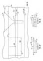
- FIG. 1Ais a side sectional view of a prior art perpendicular magnetic recording system showing a read head, a write head, and a recording medium.
- FIG. 1Bis a view in the direction 1 B- 1 B of FIG. 1A and shows the write pole (WP), the wraparound shield (WAS), and the trailing shield (TS) pad for defining the TS throat height (TH).
- WPwrite pole
- WASwraparound shield
- TStrailing shield
- FIG. 1Cis a view from the air-bearing surface (ABS) of the write head and read head in FIG. 1A and shows the WAS.
- ABSair-bearing surface
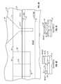
- FIG. 2Ais a view of the substrate surface of a wafer on which the write head is fabricated and shows the WP and an electrical lapping guide (ELG) layer at one point in the process of this invention.
- EMGelectrical lapping guide
- FIG. 2Bis a sectional view through plane B-B of FIG. 2A .
- FIG. 2Cis a sectional view through plane C-C of FIG. 2A .
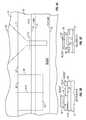
- FIG. 3Ais a view of the substrate surface of a wafer after deposition and patterning of the TS pad layer.
- FIG. 3Bis a sectional view through plane B-B of FIG. 3A .
- FIG. 3Cis a sectional view through plane C-C of FIG. 3A .
- FIG. 4Ais a view of the substrate surface of a wafer after photoresist patterning and deposition of an ELG protection layer into the opening defined the photoresist pattern.
- FIG. 4Bis a sectional view through plane B-B of FIG. 4A .
- FIG. 4Cis a sectional view through plane C-C of FIG. 4A .
- FIG. 5Ais a view of the substrate surface of a wafer after photoresist patterning to define an opening above a portion of the ELG layer to expose the TS pad layer.
- FIG. 5Bis a sectional view through plane B-B of FIG. 5A .
- FIG. 5Cis a sectional view through plane C-C of FIG. 5A .
- FIG. 6Ais a view of the substrate surface of a wafer after removal of the exposed TS pad layer over a portion of the ELG layer.
- FIG. 6Bis a sectional view through plane B-B of FIG. 6A .
- FIG. 6Cis a sectional view through plane C-C of FIG. 6A .
- FIG. 7Ais a view of the substrate surface of a wafer after removal of the ELG layer in the region not protected by the ELG protection layer and removal of the ELG protection layer, leaving the ELG layer with a back edge coincident with the front edge of the TS pad layer.
- FIG. 7Bis a sectional view through plane B-B of FIG. 7A .
- FIG. 7Cis a sectional view through plane C-C of FIG. 7A .
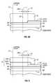
- FIG. 8Ais a view of the substrate surface of a wafer after photoresist patterning to define an opening above the WP, deposition of the TS layer into the opening and stripping of the resist.
- FIG. 8Bis a sectional view through plane B-B of FIG. 8A .
- FIG. 8Cis a sectional view through plane C-C of FIG. 8A .
- FIG. 8Dis a sectional view through plane D-D of FIG. 8A .
- FIG. 9is a sectional view corresponding generally to the view of FIG. 8D but following an alternative method according to this invention.
- FIG. 1Ais a side sectional view of a prior art perpendicular magnetic recording write head, read head and a recording medium taken through a central plane that intersects a data track on the medium.
- a “dual-layer” medium 10includes a perpendicular magnetic data recording layer (RL) 16 on a “soft” or relatively low-coercivity magnetically permeable underlayer (SUL) 14 formed on the disk substrate 12 .
- This type of mediumis shown with a single write pole type of recording or write head 30 .
- the recording head 30includes a yoke made up of the main pole 34 , flux return pole 36 , and yoke stud 38 connecting the main pole and return pole 36 ; and a thin film coil 39 shown in section wrapped around yoke stud 38 .
- a flared write pole (WP) 40is part of the main pole 34 and has a flared portion 41 and a pole tip 42 with an end 43 that faces the outer surface of medium 10 .
- Write current through coil 39induces a magnetic field (shown by dashed line 60 ) from the WP 40 that passes through the RL 16 (to magnetize the region of the RL 16 beneath the WP 40 ), through the flux return path provided by the SUL 14 , and back to the return pole 36 .
- the recording headis typically formed on a trailing surface 21 of an air-bearing slider 20 that has its air-bearing surface (ABS) supported above the surface of medium 10 .
- ABSair-bearing surface
- a magnetoresistive (MR) read head 80comprised of a MR sensing element 81 located between MR shields S 1 and S 2 is also deposited on the trailing end of the slider 20 prior to the deposition of the layers making up the write head 30 .
- trailing surface 21may be a nonmagnetic layer deposited on the MR shield S 2 .
- the medium 10moves past the recording head 30 in the direction indicated by arrow 65 , so the portion of slider 20 that supports the MR head 80 and write head 30 is often called the slider “trailing” end, and the surface perpendicular to the slider ABS on which the write head 30 is located is often called the “trailing” surface.
- the RL 16is illustrated with perpendicularly recorded or magnetized regions, with adjacent regions having opposite magnetization directions, as represented by the arrows.
- the magnetic transitions between adjacent oppositely-directed magnetized regionsare detectable by the MR sensing element 81 as the recorded bits.
- FIG. 1Aalso illustrates a trailing shield (TS) 50 and a TS pad 52 that are separated from WP 40 by a nonmagnetic gap layer 56 .
- the TS 50has a throat height (TH) defined generally as the distance between the ABS and a front edge 70 of the TS pad 52 .
- the TS 50has a total thickness defined generally by the ABS and a back edge 78 .
- the TS 50is formed of magnetically permeable material and TS pad 52 is formed of nonmagnetic material.
- the TS 50 separated from the WP 40 by nonmagnetic gap 56slightly alters the angle of the write field and makes writing more efficient.
- the portion of the TS that first receives the flux from WP 40must be very thin, for example about 50 nm.
- a nonmagnetic TS pad 52is used.
- the TS pad 52has a front edge 70 near the ABS and a back edge 71 recessed from the front edge 70 .
- the TS pad 52allows the TS to have a TH much thinner that the thickness of the remaining portion of the TS.
- a perpendicular magnetic recording write head with a TS and a TS pad, like that depicted in FIG. 1Ais described in pending application Ser. No. 11/090,456 filed Mar. 25, 2005, published as US2006/215314 A1, and assigned to the same assignee as this application.
- FIG. 1Bis a view in the direction 1 B- 1 B of FIG. 1A to illustrate the WP 40 , the TS 50 and the TS pad 52 on trailing surface 21 of slider 20 .
- the region between the WP tip 42 and the flare portion 41is called the flare point 44 .
- the flare point 44 of the WP 40is sometimes referred to as the “choke” point because it is the point where the flux density is highest and where the WP 40 saturates.
- the WP tip 42has a throat height (TH) which is generally the distance from end 43 to flare point 44 . As shown in FIG.
- the two side walls of WP tip 42define its width in the cross-track direction, which substantially defines the trackwidth (TW) of the data recorded in the RL 16 .
- the region of the WP 40 above the flare region 41is substantially wider than WP tip 42 below the flare region 41 and the flare point 44 is the transition point where the WP 40 begins to widen with distance from the ABS.
- the flare angle between flare region 41 and WP 42is between 90 and 180 degrees, typically between about 120 and 150 degrees.
- FIG. 1Balso illustrates the TS 50 and TS pad 52 .
- the portions identified as 53 , 55 on opposite ends of TS 50are side shields which, together with TS 50 form a wraparound shield (WAS) that generally surrounds the WP tip 42 .
- the TH for the TS 50is the distance from the ABS to the front edge 70 of the TS pad 52 .
- FIG. 1Cillustrates the write head 30 as seen from the recording medium 10 .
- the ABSis the recording-layer-facing surface of the slider that faces the medium 10 and is shown in FIG. 1C without the thin protective overcoat typically present in an actual slider.
- the recording-layer-facing surfaceshall mean the surface of the slider 20 that is covered with a thin protective overcoat, the actual outer surface of the slider if there is no overcoat, or the outer surface of the overcoat.
- the phrase “substantially at the recording-layer-facing surface”shall mean actually at the surface or slightly recessed from the surface.
- the recording medium 10moves relative to the head 30 in the direction 65 , which is called the along-the-track direction.
- the width of the end 43 of WP tip 42substantially defines the track-width (TW) of the data tracks in the RL 16 .
- the main pole 34is shown with dashed lines because it is recessed from the ABS (see FIG. 1A ).
- the direction perpendicular to direction 65 and parallel to the plane of the ABSis called the cross-track direction.
- the WAS that includes side shields 53 , 55 and TS 50is described in detail as a shield for a conventional perpendicular recording head in U.S. Pat. No. 7,002,775 B2 assigned to the same assignee as this application.
- the shields 50 , 53 , 55all have ends substantially at the recording-layer-facing surface.
- the shields 50 , 53 , 55are typically connected to one another and substantially surround the WP tip 42 to from the WAS.
- the TS 50 and side shields 53 , 55are separated from WP tip 42 by nonmagnetic gap material, typically alumina, which forms the gap layer 56 .
- the WAS separated from the WP tip 42 by gap layer 56alters the angle of the write field and improves the write field gradient at the point of writing, and also shields the writing field at regions of the medium 10 away from the track being written.
- the WASis shown as a “floating” shield, meaning that is not connected to the return pole 36 . However, the WAS may be connected to either the return pole 36 or other portions of the yoke by flux-conducting material. In other variations of the write head 30 , only a TS may be used without side shields. The TS may be either “floating” or connected to return pole 36 .
- FIG. 1Calso illustrates the magnetoresistive (MR) read head 80 that includes the MR sensor 81 located between MR shields S 1 , S 2 .
- the films making up MR head 80 and write head 30 as shown in FIG. 1Care formed in succession on the trailing end of air-bearing slider 20 , by a series of thin film deposition, etching and lithographic patterning processes.
- the films making up (MR) read head 80are formed on substrate surface 29 and the films making up write head 30 are formed on substrate surface 21 , which is typically a layer of nonmagnetic material, like alumina, that separates write head 30 from read head 80 .
- the yoke and shields of write head 30are formed of soft ferromagnetic material, such as alloys of NiFe, CoFe and NiFeCo that are typically formed by electroplating.
- the WP 40is formed of a high-moment material, such as a high-moment CoFe alloy, that is typically formed by sputter deposition, and may be a laminated structure.
- FIG. 2Ais a view of the substrate surface 21 of a wafer on which the write head is fabricated and shows the WP 40 at one point in the process of this invention.
- the waferis later cut into rows and the rows then cut into individual sliders.
- a line 75is shown as a cut line for separating the wafer into rows. After separation into rows, the rows are later cut into the individual sliders.
- the slidersare lapped, either individually or at the row level, to remove material between cut line 75 and line 77 , to form the ABS.
- an electrical lapping guide (ELG) layer 90 of electrically conductive materialis also formed on substrate surface 21 .
- an ELGis used to control the lapping so that lapping is stopped at the precise line desired for the ABS.
- the electrical resistanceis measured and as the ELG material is removed, lapping is terminated when the resistance reaches a predetermined value.
- the ELG layer 90is preferably gold (Au) sputter deposited to a thickness of about 25 nm, but other electrically conductive materials may also be used, such as Rh, Ru and NiCr. In the process of this invention the ELG layer 90 is used to precisely define the TH of TS 50 .
- FIG. 2Bis a sectional view through plane B-B of FIG. 2A and shows the ELG layer 90 on the substrate surface 21 .
- FIG. 2Cis a sectional view through plane C-C of FIG. 2A and shows the WP 40 and gap layer (GL) 56 on the substrate surface 21 .
- the material for the TS pad layer 52( FIG. 1A ) is then sputter deposited over the structure of FIG. 2A .
- the TS pad layer materialis preferably tantalum oxide (Ta 2 O 5 ) with a thickness of about 60-80 nm, but other nonmagnetic materials may be used, such as alumina (Al 2 O 3 ), silicon dioxide (SiO 2 ) and silicon nitride (Si 3 N 4 ).
- the structureis then patterned with photoresist to define the extent of the TS pad layer, the TS pad layer material not protected by the photoresist is removed by reactive ion etching (RIE), and the photoresist is then stripped. The resulting structure is shown in FIG.
- RIEreactive ion etching
- FIG. 3Ashows the TS pad layer (TS-PL) 52 with a front edge 70 and back edge 71 extending over the ELG layer 90 and the WP 40 .
- the region of the ELG layer 90 recessed from TS-PL front edge 70is covered with the TS-PL and the region of the ELG layer 90 between the cut line 75 and the TS-PL front edge 70 is exposed.
- FIG. 3Bis a sectional view through plane B-B of FIG. 3A and shows the ELG layer 90 and the TS-PL 52 with front edge 70 on the substrate surface 21 .
- FIG. 3Cis a sectional view through plane C-C of FIG. 3A and shows the WP 40 , GL 56 and TS-PL 52 on the substrate surface 21 .
- the structureis covered with photoresist, and the photoresist is patterned and exposed to open an area above ELG layer 90 in the region between the cut line 75 and the TS-PL front edge 70 .
- the region of the ELG layer 90 recessed from TS-PL front edge 70remains covered with the TS-PL 52 with the resist layer covering TS-PL 52 .
- An ELG protection layer 92is then deposited into the opening.
- the resulting structureis shown in FIG. 4A .
- the ELG protection layer 92is preferably a NiFe alloy electroplated to a thickness of about 50 nm onto the electrically conductive ELG layer 90 .
- Other materials that may be used for the ELG protection layer 92include NiP and CoFe.
- FIG. 4Bis a sectional view through plane B-B of FIG. 4A and shows the ELG layer 90 , the TS-PL 52 with front edge 70 , the resist layer and the ELG protection layer 92 deposited into the opening defined by the resist pattern.
- FIG. 4Cis a sectional view through plane C-C of FIG. 4A and shows the WP 40 , GL 56 and TS-PL 52 covered by the resist layer.
- FIG. 4Cis then stripped.
- the structureis again covered with photoresist, and the photoresist is patterned and exposed to open an area above ELG layer 90 in the region recessed from the TS-PL front edge 70 to expose the TS-PL 52 .
- the resulting structureis shown in FIG. 5A .
- FIG. 5Bis a sectional view through plane B-B of FIG. 5A and shows the ELG layer 90 with the exposed TS-PL 52 with front edge 70 in the opening defined by the resist pattern.
- FIG. 5Cis a sectional view through plane C-C of FIG. 5A and shows the WP 40 , GL 56 and TS-PL 52 covered by the resist layer.
- FIG. 6Ais a sectional view through plane B-B of FIG. 6A and shows the ELG layer 90 with the ELG protection layer 92 over it and having a back edge coincident with the TS-PL front edge 70 .
- FIG. 6Cis a sectional view through plane C-C of FIG. 6A and shows the WP 40 , GL 56 and TS-PL 52 .
- a layer of photoresistis then deposited over the structure of FIG. 6A and patterned to expose the entire ELG layer 90 , i.e., both the portion between the cut line 75 and TS-PL front edge 70 that is covered with the ELG protection layer 92 and the portion recessed from TS-PL front edge 70 .
- the WP 40is protected by the resist layer.
- the ELG layer 90is then ion milled using Ar ions and end point detection (EPD) on the ELG layer material. This removes all of the ELG layer 92 except that portion protected by the ELG protection layer 92 , which acts as a milling mask. The ion milling does not affect the WP 40 which is protected by the resist layer.
- FIG. 7Ais a sectional view through plane B-B of FIG. 7A and shows the ELG layer 90 with its back edge 93 coincident with the TS-PL front edge 70 .
- the TS THis defined by the ABS (line 77 ) and the TS-PL front edge 70 , which is now aligned with the back edge 93 of ELG layer 92 .
- FIG. 7Cis a sectional view through plane C-C of FIG. 7A and shows the WP 40 , GL 56 and TS-PL 52 .
- FIG. 8Ais a sectional view through plane B-B of FIG.
- FIG. 8Aand shows the ELG layer 90 with its back edge 93 coincident with the TS-PL front edge 70 .
- FIG. 8Cis a sectional view through plane C-C of FIG. 8A and shows the WP 40 , GL 56 , TS-PL 52 , the seed layer, and the TS layer 50 .
- FIG. 8Dis a sectional view through plane D-D of FIG. 8A and shows the TS and the definition of TS TH between the ABS and line 70 .
- the waferis cut along line 75 and then lapped.
- the lappingmay be done on a row of wafers, or at the individual slider level after the sliders are cut from the rows.
- the lappingis performed along a plane parallel to cut line 75 and perpendicular to the substrate surface 21 , and in the direction shown by the arrow in FIG. 8D .
- the electrical resistance of ELG layer 90is monitored. The resistance decreases generally proportionally with the amount of ELG material that is removed.
- the electrical resistance of the amount of ELG material between line 77 and back edge 93( FIG. 8A ) is known.
- lapping stopsThis defines generally the ABS and thus the TS TH because the back edge 93 has been aligned with the front edge 70 of the TS-PL 52 .
- FIG. 9is a view at the end of the alternative method, corresponding to FIG. 8D .
- This methodtakes advantage of the fact that the ELG protection layer 92 can be formed of NiFe, the same material that can be used for the TS.
- a first TS layer 50 ais formed during the steps shown in FIG. 4A by also patterning the resist to define an opening above WP 40 to define the first TS layer 50 a .
- the NiFeis then electroplated into both openings so that ELG protection layer 92 and the first TS layer 50 a are formed at the same time.
- the ELG layer 90is protected with resist and a thin CoFe layer is deposited over the WP 40 to cover the first TS layer 50 a and the TS-PL 52 , as shown in FIG. 9 .
- the TS-PL layer 52is then removed in the ELG region as described and shown in FIG. 6A .
- the structureis covered with photoresist and the photoresist patterned to define an opening above WP 40 to deposit the second TS layer 50 b . This opening is defined along line 78 which is to be the back edge for the second TS layer 50 b .
- the material of second TS layer 50 bis then electroplated into this opening onto the thin CoFe layer and the resist is stripped.
- the material of the second TS layeris preferably a material that has a lower magnetic moment than the material of the first TS layer.
- the first TS layer 50 a used as the ELG protection layermay be Ni22Fe78 and the second TS layer 50 b may be a NiFe material with a lower magnetic moment, like Ni45Fe55 or Ni80Fe20.
- the first and second TS layersmay also be formed of material with the same or similar moments.
- the ELG layer 90is ion milled to leave only the portion protected by the ELG protection layer 92 , which acts as a milling mask, and then the ELG protection layer 92 is removed by RIE.
Landscapes
- Engineering & Computer Science (AREA)
- Manufacturing & Machinery (AREA)
- Physics & Mathematics (AREA)
- Electromagnetism (AREA)
- Magnetic Heads (AREA)
Abstract
Description
Claims (9)
Priority Applications (1)
| Application Number | Priority Date | Filing Date | Title |
|---|---|---|---|
| US11/746,856US7770281B2 (en) | 2007-05-10 | 2007-05-10 | Method for redefining the trailing shield throat height in a perpendicular magnetic recording write head |
Applications Claiming Priority (1)
| Application Number | Priority Date | Filing Date | Title |
|---|---|---|---|
| US11/746,856US7770281B2 (en) | 2007-05-10 | 2007-05-10 | Method for redefining the trailing shield throat height in a perpendicular magnetic recording write head |
Publications (2)
| Publication Number | Publication Date |
|---|---|
| US20080276448A1 US20080276448A1 (en) | 2008-11-13 |
| US7770281B2true US7770281B2 (en) | 2010-08-10 |
Family
ID=39968202
Family Applications (1)
| Application Number | Title | Priority Date | Filing Date |
|---|---|---|---|
| US11/746,856Expired - Fee RelatedUS7770281B2 (en) | 2007-05-10 | 2007-05-10 | Method for redefining the trailing shield throat height in a perpendicular magnetic recording write head |
Country Status (1)
| Country | Link |
|---|---|
| US (1) | US7770281B2 (en) |
Cited By (12)
| Publication number | Priority date | Publication date | Assignee | Title |
|---|---|---|---|---|
| US20090091861A1 (en)* | 2007-10-03 | 2009-04-09 | Headway Technologies, Inc. | Perpendicular magnetic recording write head with a side shield |
| US20090268348A1 (en)* | 2008-04-28 | 2009-10-29 | Christian Rene Bonhote | Write head lapping guide about aligned to a non-magnetic layer surrounding a write pole and a method for making the same |
| US8151441B1 (en) | 2008-03-27 | 2012-04-10 | Western Digital (Fremont), Llc | Method for providing and utilizing an electronic lapping guide in a magnetic recording transducer |
| US8165709B1 (en) | 2009-02-26 | 2012-04-24 | Western Digital (Fremont), Llc | Four pad self-calibrating electronic lapping guide |
| US8291743B1 (en) | 2009-05-27 | 2012-10-23 | Western Digital (Fremont), Llc | Method and system for calibrating an electronic lapping guide for a beveled pole in a magnetic recording transducer |
| US8307539B1 (en) | 2009-09-30 | 2012-11-13 | Western Digital (Fremont), Llc | Method for modeling devices in a wafer |
| US8443510B1 (en)* | 2009-05-28 | 2013-05-21 | Western Digital (Fremont), Llc | Method for utilizing an electronic lapping guide for a beveled pole in a magnetic recording transducer |
| US8628672B1 (en) | 2012-06-27 | 2014-01-14 | Western Digital (Fremont), Llc | Process for manufacturing a perpendicular magnetic recording writer pole with nonmagnetic bevel |
| US8797686B1 (en) | 2010-12-23 | 2014-08-05 | Western Digital (Fremont), Llc | Magnetic recording transducer with short effective throat height and method of fabrication |
| US9042051B2 (en) | 2013-08-15 | 2015-05-26 | Western Digital (Fremont), Llc | Gradient write gap for perpendicular magnetic recording writer |
| US9082426B1 (en)* | 2012-12-19 | 2015-07-14 | Western Digital (Fremont), Llc | Methods for manufacturing electronic lapping guides for writer heads that closely track pole formation of the writer heads |
| US9082423B1 (en) | 2013-12-18 | 2015-07-14 | Western Digital (Fremont), Llc | Magnetic recording write transducer having an improved trailing surface profile |
Families Citing this family (4)
| Publication number | Priority date | Publication date | Assignee | Title |
|---|---|---|---|---|
| US8257597B1 (en) | 2010-03-03 | 2012-09-04 | Western Digital (Fremont), Llc | Double rie damascene process for nose length control |
| US8453317B2 (en) | 2010-10-14 | 2013-06-04 | HGST Netherlands, B.V. | Magnetic write head fabrication with integrated electrical lapping guides |
| US20120262824A1 (en)* | 2011-04-14 | 2012-10-18 | International Business Machines Corporation | Magnetic write head with structured trailing pole |
| US11594247B1 (en)* | 2022-02-28 | 2023-02-28 | Western Digital Technologies, Inc. | Slider air bearing designs with higher pressure and higher thermal flying height (TFC) efficiency |
Citations (9)
| Publication number | Priority date | Publication date | Assignee | Title |
|---|---|---|---|---|
| USRE33949E (en)* | 1985-01-22 | 1992-06-02 | Digital Equipment Corporation | Vertical magnetic recording arrangement |
| US6884148B1 (en)* | 2004-05-26 | 2005-04-26 | Headway Technologies, Inc. | Independently controlled read and write head stripe height parameters in slider back end process |
| US20050243464A1 (en)* | 2004-04-30 | 2005-11-03 | Lille Jeffrey S | Magnetic write head having a notched yoke structure with a trailing shield and method of making the same |
| US20050264931A1 (en)* | 2004-05-25 | 2005-12-01 | Hitachi Global Storage Technologies Netherlands, B.V | Notched trailing shield for perpendicular write head |
| US7002775B2 (en) | 2003-09-30 | 2006-02-21 | Hitachi Global Storage Technologies Netherlands B.V. | Head for perpendicular magnetic recording with a shield structure connected to the return pole piece |
| US20060044683A1 (en)* | 2004-09-01 | 2006-03-02 | Sae Magnetics (H.K.) Ltd. | Thin film magnetic head structure, method of manufacturing the same, and method of manufacturing thin film magnetic head |
| US20060168798A1 (en)* | 2005-01-31 | 2006-08-03 | Kabushiki Kaisha Toshiba | Method of lapping row bar in which perpendicular magnetic heads are formed and lapping machine |
| US20060215314A1 (en)* | 2005-03-25 | 2006-09-28 | Chen Tsung Y | Magnetic write head with trailing shield throat pad |
| US7140095B2 (en) | 2003-03-31 | 2006-11-28 | Sae Magnetics (H.K.) Ltd. | Method of manufacturing a thin film magnetic head |
- 2007
- 2007-05-10USUS11/746,856patent/US7770281B2/ennot_activeExpired - Fee Related
Patent Citations (9)
| Publication number | Priority date | Publication date | Assignee | Title |
|---|---|---|---|---|
| USRE33949E (en)* | 1985-01-22 | 1992-06-02 | Digital Equipment Corporation | Vertical magnetic recording arrangement |
| US7140095B2 (en) | 2003-03-31 | 2006-11-28 | Sae Magnetics (H.K.) Ltd. | Method of manufacturing a thin film magnetic head |
| US7002775B2 (en) | 2003-09-30 | 2006-02-21 | Hitachi Global Storage Technologies Netherlands B.V. | Head for perpendicular magnetic recording with a shield structure connected to the return pole piece |
| US20050243464A1 (en)* | 2004-04-30 | 2005-11-03 | Lille Jeffrey S | Magnetic write head having a notched yoke structure with a trailing shield and method of making the same |
| US20050264931A1 (en)* | 2004-05-25 | 2005-12-01 | Hitachi Global Storage Technologies Netherlands, B.V | Notched trailing shield for perpendicular write head |
| US6884148B1 (en)* | 2004-05-26 | 2005-04-26 | Headway Technologies, Inc. | Independently controlled read and write head stripe height parameters in slider back end process |
| US20060044683A1 (en)* | 2004-09-01 | 2006-03-02 | Sae Magnetics (H.K.) Ltd. | Thin film magnetic head structure, method of manufacturing the same, and method of manufacturing thin film magnetic head |
| US20060168798A1 (en)* | 2005-01-31 | 2006-08-03 | Kabushiki Kaisha Toshiba | Method of lapping row bar in which perpendicular magnetic heads are formed and lapping machine |
| US20060215314A1 (en)* | 2005-03-25 | 2006-09-28 | Chen Tsung Y | Magnetic write head with trailing shield throat pad |
Cited By (17)
| Publication number | Priority date | Publication date | Assignee | Title |
|---|---|---|---|---|
| US8035930B2 (en)* | 2007-10-03 | 2011-10-11 | Headway Technologies, Inc. | Perpendicular magnetic recording write head with a side shield |
| US20090091861A1 (en)* | 2007-10-03 | 2009-04-09 | Headway Technologies, Inc. | Perpendicular magnetic recording write head with a side shield |
| US8151441B1 (en) | 2008-03-27 | 2012-04-10 | Western Digital (Fremont), Llc | Method for providing and utilizing an electronic lapping guide in a magnetic recording transducer |
| US9153260B1 (en) | 2008-03-27 | 2015-10-06 | Western Digital (Fremont), Llc | Electronic lapping guide in a magnetic recording transducer |
| US20090268348A1 (en)* | 2008-04-28 | 2009-10-29 | Christian Rene Bonhote | Write head lapping guide about aligned to a non-magnetic layer surrounding a write pole and a method for making the same |
| US8161627B2 (en)* | 2008-04-28 | 2012-04-24 | Hitachi Global Storage Technologies Netherlands B.V. | Method of making a write head lapping guide about aligned to a non-magnetic layer surrounding a write pole |
| US8165709B1 (en) | 2009-02-26 | 2012-04-24 | Western Digital (Fremont), Llc | Four pad self-calibrating electronic lapping guide |
| US8717709B1 (en) | 2009-05-27 | 2014-05-06 | Western Digital (Fremont), Llc | System for calibrating an electronic lapping guide for a beveled pole in a magnetic recording transducer |
| US8291743B1 (en) | 2009-05-27 | 2012-10-23 | Western Digital (Fremont), Llc | Method and system for calibrating an electronic lapping guide for a beveled pole in a magnetic recording transducer |
| US8443510B1 (en)* | 2009-05-28 | 2013-05-21 | Western Digital (Fremont), Llc | Method for utilizing an electronic lapping guide for a beveled pole in a magnetic recording transducer |
| US8307539B1 (en) | 2009-09-30 | 2012-11-13 | Western Digital (Fremont), Llc | Method for modeling devices in a wafer |
| US8797686B1 (en) | 2010-12-23 | 2014-08-05 | Western Digital (Fremont), Llc | Magnetic recording transducer with short effective throat height and method of fabrication |
| US8628672B1 (en) | 2012-06-27 | 2014-01-14 | Western Digital (Fremont), Llc | Process for manufacturing a perpendicular magnetic recording writer pole with nonmagnetic bevel |
| US9082426B1 (en)* | 2012-12-19 | 2015-07-14 | Western Digital (Fremont), Llc | Methods for manufacturing electronic lapping guides for writer heads that closely track pole formation of the writer heads |
| US9042051B2 (en) | 2013-08-15 | 2015-05-26 | Western Digital (Fremont), Llc | Gradient write gap for perpendicular magnetic recording writer |
| US9214166B1 (en) | 2013-08-15 | 2015-12-15 | Western Digital (Fremont), Llc | Gradient write gap for perpendicular magnetic recording writer |
| US9082423B1 (en) | 2013-12-18 | 2015-07-14 | Western Digital (Fremont), Llc | Magnetic recording write transducer having an improved trailing surface profile |
Also Published As
| Publication number | Publication date |
|---|---|
| US20080276448A1 (en) | 2008-11-13 |
Similar Documents
| Publication | Publication Date | Title |
|---|---|---|
| US7770281B2 (en) | Method for redefining the trailing shield throat height in a perpendicular magnetic recording write head | |
| US7995307B2 (en) | Perpendicular magnetic recording write head with trailing shield having throat height defined by electroplated nonmagnetic pad layer and method for making the head | |
| US7768743B2 (en) | Perpendicular magnetic recording write head with trailing shield having notch and throat height defined by nonmagnetic pad layer | |
| US7920358B2 (en) | Perpendicular magnetic recording write head with magnetic shields separated by nonmagnetic layers | |
| US8018679B2 (en) | Perpendicular magnetic recording write head with slanted magnetic write pole | |
| US7889456B2 (en) | Perpendicular magnetic recording write head with flux shaping layers on the write pole and magnetic recording system incorporating the write head | |
| US7748103B2 (en) | Method of manufacturing a perpendicular magnetic recording write head with notched trailing shield | |
| US8051552B2 (en) | Stitched wrap around shield fabrication for perpendicular magnetic recording write heads | |
| US7788796B2 (en) | Method FPR manufacturing a magnetic write head | |
| US8634162B2 (en) | Perpendicular write head having a stepped flare structure and method of manufacture thereof | |
| US8498078B2 (en) | Magnetic head with flared write pole having multiple tapered regions | |
| US8451560B2 (en) | Magnetic head with flared write pole with multiple non-magnetic layers thereover | |
| US8108985B2 (en) | Method for manufacturing a perpendicular magnetic write head | |
| US7377024B2 (en) | Method of making a magnetic write head with trailing shield throat pad | |
| US20080316652A1 (en) | Simultaneous pole-tip and side shield fabrication and integrated elg | |
| US8568601B2 (en) | Fenceless main pole definition for advanced perpendicular magnetic write head | |
| US8136228B2 (en) | Method for manufacturing a magnetic write head | |
| US9236069B2 (en) | Method for making a current-perpendicular-to-the-plane (CPP) magnetoresistive (MR) sensor with reduced-width self-aligned top electrode | |
| JP2001167408A (en) | Thin-film magnetic head and method for manufacturing the same | |
| US6900963B1 (en) | Thin film magnetic head with track width restricting groove formed to fully reach lower core layer, and manufacturing method for the same | |
| JP3475148B2 (en) | Thin film magnetic head and method of manufacturing the same | |
| US7500303B2 (en) | Method of fabricating a magnetic sensor on a wafer |
Legal Events
| Date | Code | Title | Description |
|---|---|---|---|
| AS | Assignment | Owner name:HITACHI GLOBAL STORAGE TECHNOLOGIES NETHERLANDS B. Free format text:ASSIGNMENT OF ASSIGNORS INTEREST;ASSIGNOR:PENTEK, ARON;REEL/FRAME:019276/0181 Effective date:20070510 | |
| FEPP | Fee payment procedure | Free format text:PAYOR NUMBER ASSIGNED (ORIGINAL EVENT CODE: ASPN); ENTITY STATUS OF PATENT OWNER: LARGE ENTITY | |
| STCF | Information on status: patent grant | Free format text:PATENTED CASE | |
| AS | Assignment | Owner name:HGST, NETHERLANDS B.V., NETHERLANDS Free format text:CHANGE OF NAME;ASSIGNOR:HGST, NETHERLANDS B.V.;REEL/FRAME:029341/0777 Effective date:20120723 Owner name:HGST NETHERLANDS B.V., NETHERLANDS Free format text:CHANGE OF NAME;ASSIGNOR:HITACHI GLOBAL STORAGE TECHNOLOGIES NETHERLANDS B.V.;REEL/FRAME:029341/0777 Effective date:20120723 | |
| FPAY | Fee payment | Year of fee payment:4 | |
| AS | Assignment | Owner name:WESTERN DIGITAL TECHNOLOGIES, INC., CALIFORNIA Free format text:ASSIGNMENT OF ASSIGNORS INTEREST;ASSIGNOR:HGST NETHERLANDS B.V.;REEL/FRAME:040821/0550 Effective date:20160831 | |
| MAFP | Maintenance fee payment | Free format text:PAYMENT OF MAINTENANCE FEE, 8TH YEAR, LARGE ENTITY (ORIGINAL EVENT CODE: M1552) Year of fee payment:8 | |
| AS | Assignment | Owner name:JPMORGAN CHASE BANK, N.A., AS AGENT, ILLINOIS Free format text:SECURITY INTEREST;ASSIGNOR:WESTERN DIGITAL TECHNOLOGIES, INC.;REEL/FRAME:052915/0566 Effective date:20200113 | |
| AS | Assignment | Owner name:WESTERN DIGITAL TECHNOLOGIES, INC., CALIFORNIA Free format text:RELEASE OF SECURITY INTEREST AT REEL 052915 FRAME 0566;ASSIGNOR:JPMORGAN CHASE BANK, N.A.;REEL/FRAME:059127/0001 Effective date:20220203 | |
| FEPP | Fee payment procedure | Free format text:MAINTENANCE FEE REMINDER MAILED (ORIGINAL EVENT CODE: REM.); ENTITY STATUS OF PATENT OWNER: LARGE ENTITY | |
| LAPS | Lapse for failure to pay maintenance fees | Free format text:PATENT EXPIRED FOR FAILURE TO PAY MAINTENANCE FEES (ORIGINAL EVENT CODE: EXP.); ENTITY STATUS OF PATENT OWNER: LARGE ENTITY | |
| STCH | Information on status: patent discontinuation | Free format text:PATENT EXPIRED DUE TO NONPAYMENT OF MAINTENANCE FEES UNDER 37 CFR 1.362 | |
| FP | Lapsed due to failure to pay maintenance fee | Effective date:20220810 |