US7768868B2 - Digital filters for semiconductor devices - Google Patents
Digital filters for semiconductor devicesDownload PDFInfo
- Publication number
- US7768868B2 US7768868B2US11/820,007US82000707AUS7768868B2US 7768868 B2US7768868 B2US 7768868B2US 82000707 AUS82000707 AUS 82000707AUS 7768868 B2US7768868 B2US 7768868B2
- Authority
- US
- United States
- Prior art keywords
- counter
- coupled
- data storage
- bit
- internal data
- Prior art date
- Legal status (The legal status is an assumption and is not a legal conclusion. Google has not performed a legal analysis and makes no representation as to the accuracy of the status listed.)
- Active, expires
Links
- 239000004065semiconductorSubstances0.000titleclaimsdescription4
- 239000003990capacitorSubstances0.000claimsdescription39
- 238000013500data storageMethods0.000claimsdescription21
- 238000000034methodMethods0.000claimsdescription12
- 239000004020conductorSubstances0.000claimsdescription10
- 238000001914filtrationMethods0.000claimsdescription5
- 238000003384imaging methodMethods0.000description12
- 238000007599dischargingMethods0.000description7
- 238000013461designMethods0.000description5
- 230000000694effectsEffects0.000description5
- 230000007704transitionEffects0.000description4
- 238000004891communicationMethods0.000description3
- 238000004519manufacturing processMethods0.000description3
- 230000003071parasitic effectEffects0.000description3
- 238000011161developmentMethods0.000description2
- 230000006870functionEffects0.000description2
- 230000000977initiatory effectEffects0.000description2
- 239000011159matrix materialSubstances0.000description2
- 238000005259measurementMethods0.000description2
- 238000012986modificationMethods0.000description2
- 230000004048modificationEffects0.000description2
- 230000008569processEffects0.000description2
- 238000012545processingMethods0.000description2
- 230000004044responseEffects0.000description2
- 230000035945sensitivityEffects0.000description2
- 238000012935AveragingMethods0.000description1
- 230000008901benefitEffects0.000description1
- 238000004364calculation methodMethods0.000description1
- 230000001413cellular effectEffects0.000description1
- 235000019504cigarettesNutrition0.000description1
- 230000008878couplingEffects0.000description1
- 238000010168coupling processMethods0.000description1
- 238000005859coupling reactionMethods0.000description1
- 230000003247decreasing effectEffects0.000description1
- 230000001419dependent effectEffects0.000description1
- 238000010586diagramMethods0.000description1
- 230000005684electric fieldEffects0.000description1
- 239000000446fuelSubstances0.000description1
- 239000002784hot electronSubstances0.000description1
- 238000002347injectionMethods0.000description1
- 239000007924injectionSubstances0.000description1
- 230000002093peripheral effectEffects0.000description1
- 230000000630rising effectEffects0.000description1
- 238000005070samplingMethods0.000description1
- 230000003068static effectEffects0.000description1
- 230000001360synchronised effectEffects0.000description1
- 238000012546transferMethods0.000description1
- 230000001052transient effectEffects0.000description1
- 230000001960triggered effectEffects0.000description1
- 230000005641tunnelingEffects0.000description1
Images


Classifications
- G—PHYSICS
- G11—INFORMATION STORAGE
- G11C—STATIC STORES
- G11C16/00—Erasable programmable read-only memories
- G11C16/02—Erasable programmable read-only memories electrically programmable
- G11C16/06—Auxiliary circuits, e.g. for writing into memory
- G11C16/26—Sensing or reading circuits; Data output circuits
- G—PHYSICS
- G11—INFORMATION STORAGE
- G11C—STATIC STORES
- G11C11/00—Digital stores characterised by the use of particular electric or magnetic storage elements; Storage elements therefor
- G11C11/56—Digital stores characterised by the use of particular electric or magnetic storage elements; Storage elements therefor using storage elements with more than two stable states represented by steps, e.g. of voltage, current, phase, frequency
- G11C11/5621—Digital stores characterised by the use of particular electric or magnetic storage elements; Storage elements therefor using storage elements with more than two stable states represented by steps, e.g. of voltage, current, phase, frequency using charge storage in a floating gate
- G11C11/5642—Sensing or reading circuits; Data output circuits
- G—PHYSICS
- G11—INFORMATION STORAGE
- G11C—STATIC STORES
- G11C11/00—Digital stores characterised by the use of particular electric or magnetic storage elements; Storage elements therefor
- G11C11/56—Digital stores characterised by the use of particular electric or magnetic storage elements; Storage elements therefor using storage elements with more than two stable states represented by steps, e.g. of voltage, current, phase, frequency
- G11C11/5678—Digital stores characterised by the use of particular electric or magnetic storage elements; Storage elements therefor using storage elements with more than two stable states represented by steps, e.g. of voltage, current, phase, frequency using amorphous/crystalline phase transition storage elements
- G—PHYSICS
- G11—INFORMATION STORAGE
- G11C—STATIC STORES
- G11C16/00—Erasable programmable read-only memories
- G11C16/02—Erasable programmable read-only memories electrically programmable
- G11C16/04—Erasable programmable read-only memories electrically programmable using variable threshold transistors, e.g. FAMOS
- G11C16/0483—Erasable programmable read-only memories electrically programmable using variable threshold transistors, e.g. FAMOS comprising cells having several storage transistors connected in series
- G—PHYSICS
- G11—INFORMATION STORAGE
- G11C—STATIC STORES
- G11C27/00—Electric analogue stores, e.g. for storing instantaneous values
- G11C27/005—Electric analogue stores, e.g. for storing instantaneous values with non-volatile charge storage, e.g. on floating gate or MNOS
- G—PHYSICS
- G11—INFORMATION STORAGE
- G11C—STATIC STORES
- G11C29/00—Checking stores for correct operation ; Subsequent repair; Testing stores during standby or offline operation
- G11C29/02—Detection or location of defective auxiliary circuits, e.g. defective refresh counters
- G—PHYSICS
- G11—INFORMATION STORAGE
- G11C—STATIC STORES
- G11C29/00—Checking stores for correct operation ; Subsequent repair; Testing stores during standby or offline operation
- G11C29/02—Detection or location of defective auxiliary circuits, e.g. defective refresh counters
- G11C29/023—Detection or location of defective auxiliary circuits, e.g. defective refresh counters in clock generator or timing circuitry
- G—PHYSICS
- G11—INFORMATION STORAGE
- G11C—STATIC STORES
- G11C29/00—Checking stores for correct operation ; Subsequent repair; Testing stores during standby or offline operation
- G11C29/02—Detection or location of defective auxiliary circuits, e.g. defective refresh counters
- G11C29/028—Detection or location of defective auxiliary circuits, e.g. defective refresh counters with adaption or trimming of parameters
- G—PHYSICS
- G11—INFORMATION STORAGE
- G11C—STATIC STORES
- G11C7/00—Arrangements for writing information into, or reading information out from, a digital store
- G11C7/02—Arrangements for writing information into, or reading information out from, a digital store with means for avoiding parasitic signals
- G—PHYSICS
- G11—INFORMATION STORAGE
- G11C—STATIC STORES
- G11C7/00—Arrangements for writing information into, or reading information out from, a digital store
- G11C7/06—Sense amplifiers; Associated circuits, e.g. timing or triggering circuits
- G11C7/067—Single-ended amplifiers
- G—PHYSICS
- G11—INFORMATION STORAGE
- G11C—STATIC STORES
- G11C7/00—Arrangements for writing information into, or reading information out from, a digital store
- G11C7/10—Input/output [I/O] data interface arrangements, e.g. I/O data control circuits, I/O data buffers
- G11C7/1006—Data managing, e.g. manipulating data before writing or reading out, data bus switches or control circuits therefor
- G—PHYSICS
- G11—INFORMATION STORAGE
- G11C—STATIC STORES
- G11C7/00—Arrangements for writing information into, or reading information out from, a digital store
- G11C7/10—Input/output [I/O] data interface arrangements, e.g. I/O data control circuits, I/O data buffers
- G11C7/1051—Data output circuits, e.g. read-out amplifiers, data output buffers, data output registers, data output level conversion circuits
- G11C7/106—Data output latches
- G—PHYSICS
- G11—INFORMATION STORAGE
- G11C—STATIC STORES
- G11C7/00—Arrangements for writing information into, or reading information out from, a digital store
- G11C7/10—Input/output [I/O] data interface arrangements, e.g. I/O data control circuits, I/O data buffers
- G11C7/1051—Data output circuits, e.g. read-out amplifiers, data output buffers, data output registers, data output level conversion circuits
- G11C7/1069—I/O lines read out arrangements
- G—PHYSICS
- G11—INFORMATION STORAGE
- G11C—STATIC STORES
- G11C13/00—Digital stores characterised by the use of storage elements not covered by groups G11C11/00, G11C23/00, or G11C25/00
- G11C13/0002—Digital stores characterised by the use of storage elements not covered by groups G11C11/00, G11C23/00, or G11C25/00 using resistive RAM [RRAM] elements
- G11C13/0004—Digital stores characterised by the use of storage elements not covered by groups G11C11/00, G11C23/00, or G11C25/00 using resistive RAM [RRAM] elements comprising amorphous/crystalline phase transition cells
- G—PHYSICS
- G11—INFORMATION STORAGE
- G11C—STATIC STORES
- G11C16/00—Erasable programmable read-only memories
- G11C16/02—Erasable programmable read-only memories electrically programmable
- G11C16/04—Erasable programmable read-only memories electrically programmable using variable threshold transistors, e.g. FAMOS
- G—PHYSICS
- G11—INFORMATION STORAGE
- G11C—STATIC STORES
- G11C2211/00—Indexing scheme relating to digital stores characterized by the use of particular electric or magnetic storage elements; Storage elements therefor
- G11C2211/56—Indexing scheme relating to G11C11/56 and sub-groups for features not covered by these groups
- G11C2211/563—Multilevel memory reading aspects
- G11C2211/5634—Reference cells
- G—PHYSICS
- G11—INFORMATION STORAGE
- G11C—STATIC STORES
- G11C2211/00—Indexing scheme relating to digital stores characterized by the use of particular electric or magnetic storage elements; Storage elements therefor
- G11C2211/56—Indexing scheme relating to G11C11/56 and sub-groups for features not covered by these groups
- G11C2211/564—Miscellaneous aspects
- G11C2211/5644—Multilevel memory comprising counting devices
Definitions
- Embodiments of the present inventionrelate generally to digital filters, and, more specifically, to digital filters for sensing multi-bit memory elements or multi-level image sensors.
- memory devicesinclude an array of memory elements and associated sense amplifiers.
- the memory elementsstore data
- the sense amplifiersread the data from the memory elements.
- a currentis passed through the memory element, and the current or a resulting voltage is measured by the sense amplifier.
- the sense amplifiermeasures the current or voltage by comparing it to a reference current or voltage. Depending on whether the current or voltage is greater than the reference, the sense amplifier outputs a value of one or zero. That is, the sense amplifier quantizes or digitizes the analog signal from the memory element into one of two logic states.
- memory elementsare capable of assuming more than just two states. That is, some memory elements are capable of multi-bit storage. For instance, rather than outputting either a high or low voltage, the memory element may output four or eight different voltage levels, each level corresponding to a different data value.
- conventional sense amplifiersoften fail to distinguish accurately between the additional levels because the difference between the levels (e.g., a voltage difference) in a multi-bit memory element is often smaller than the difference between the levels in a single-bit memory element. Thus, conventional sense amplifiers often can not read multi-bit memory elements.
- noise in the power supply, ground, and reference voltagemay cause an inaccurate reading of the memory element.
- the noisemay have a variety of sources, such as temperature variations, parasitic signals, data dependent effects, and manufacturing process variations. This susceptibility to noise often leads a designer to reduce the number of readable states of the memory element, which tends to reduce memory density and increase the cost of memory.
- FIG. 1illustrates an electronic device in accordance with an embodiment of the present invention
- FIG. 2illustrates a memory device in accordance with an embodiment of the present invention
- FIG. 3illustrates a memory array in accordance with an embodiment of the present invention
- FIG. 4illustrates a memory element in accordance with an embodiment of the present invention
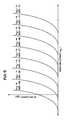
- FIG. 5illustrates I-V traces of memory elements storing different values, in accordance with an embodiment of the present invention
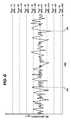
- FIG. 6illustrates noise in the bit-line current during a read operation, in accordance with an embodiment of the present invention
- FIG. 7illustrates a quantizing circuit in accordance with an embodiment of the present invention
- FIG. 8illustrates a delta-sigma sensing circuit in accordance with an embodiment of the present invention
- FIGS. 9 and 10illustrate current flow during operation of the quantizing circuit of FIG. 8 ;
- FIGS. 11-13illustrate voltages in the quantizing circuit of FIG. 8 when sensing small, medium, and large currents, respectively;
- FIG. 14is a graph of bit-line current versus counter output for the quantizing circuit of FIG. 8 ;
- FIG. 15illustrates an example of a divider for a digital filter in accordance with an embodiment of the present invention
- FIG. 16is a graph of count versus digital filter output for the quantizing circuit of FIG. 15 .
- FIG. 17is flow chart of a read operation in accordance with an embodiment of the present invention.
- FIG. 18is flow chart of a write operation in accordance with an embodiment of the present invention.
- FIG. 19is an example of a system that includes the memory device of FIG. 2 in accordance with an embodiment of the present invention.
- Some of the subsequently described embodimentsmay address one or more of the problems with conventional sense amplifiers discussed above.
- Some embodimentsinclude a quantizing circuit configured to detect small differences in voltages and/or current by quantizing the signal and then digitally filtering noise from the quantized signal.
- an analog-to-digital converteroutputs a pulse-density modulated bit-stream that represents the analog signal, and a digital filter integrates the bit-stream in a first filtration step.
- the digital filterthen performs a second filtration step whereby an average value is calculated from the integral of the bit-stream.
- the quantizing circuitmay resolve small differences between voltage or current levels in multi-bit memory elements and/or light sensors, which may allow circuit designers to increase the number of bits stored per memory element and/or the sensitivity of an imaging device.
- FIG. 1depicts an electronic device 10 in accordance with one or more of the present techniques.
- the illustrated electronic device 10includes a memory device 12 that, as explained further below, may include multi-bit memory elements and quantizing circuits. Alternatively, or additionally, the electronic device 10 may include an imaging device 13 having the quantizing circuits.
- the electronic device 10may be a storage device, a communications device, an entertainment device, an imaging system, or a computer system, such as a personal computer, a server, a mainframe, a tablet computer, a palm-top computer, or a laptop.
- a computer systemsuch as a personal computer, a server, a mainframe, a tablet computer, a palm-top computer, or a laptop.
- FIG. 2depicts a block diagram of an embodiment of the memory device 12 .
- the illustrated memory device 12may include a memory array 14 , a quantizing circuit 16 , a column decoder 18 , a column address latch 20 , row drivers 22 , a row decoder 24 , row address latches 26 , and control circuitry 28 .
- the memory array 14may include a matrix of memory elements arrayed in rows and columns.
- the imaging device 13may include similar features except that in the case of the imaging device 13 ( FIG. 1 ), the memory array 14 will include a matrix of imaging elements.
- the control circuitrymay receive a command to read from or write to a target memory address.
- the control circuitry 28may then convert the target address into a row address and a column address.
- the row address bus 30transmits the row address to the row address latches 26
- a column address bus 32transmits column address to the column address latches 20 .
- a row address strobe (RAS) signal 34(or other controlling clock signal) may be asserted by the control circuitry 28 , and the row address latches 26 may latch the transmitted row address.
- the control circuitry 28may assert a column address strobe 36 , and the column address latches 20 may latch the transmitted column address.
- the row decoder 24may determine which row of the memory array 14 corresponds to the latched row address, and the row drivers 22 may assert a signal on the selected row.
- the column decoder 18may determine which column of the memory array 14 corresponds with the latched column address, and the quantizing circuit 16 may sense a voltage or current on the selected column. Additional details of reading and writing are described below.
- FIG. 3illustrates an example of a memory array 14 .
- the illustrated memory array 14includes a plurality of bit-lines 38 , 40 , 42 , 44 , and 46 (also referred to as BL 0 -BL 4 ) and a plurality of word-lines 48 , 50 , 52 , 54 , 56 , 58 , 60 , and 62 (also referred to as WL 0 -WL 7 ). These bit-lines and word-lines are electrical conductors.
- the memory array 14further includes a plurality of memory elements 64 , each of which may be arranged to intersect one of the bit-lines and one of the word-lines. In other embodiments, imaging elements may be disposed at each of these intersections.
- the illustrated memory elements 64are flash memory devices. The operation of the flash memory elements is described further below with reference to the FIGS. 4 and 5 . It should be noted that, in other embodiments, the memory elements 64 may include other types of volatile or nonvolatile memory.
- the memory elements 64may include a resistive memory, such as a phase-change memory or magnetoresistive memory.
- the memory elements 64may include a capacitor, such as a stacked or trench capacitor.
- Some types of memory elements 64may include an access device, such as a transistor or a diode associated with each of the memory elements 64 , or the memory elements 64 may not include an access device, for instance in a cross-point array.
- FIG. 4illustrates a circuit 66 that models the operation of an arbitrarily selected memory element 64 , which is disposed at the intersection of WL 3 and BL 0 .
- This circuit 66includes a capacitor 68 , a pre-drain resistor 70 (R PD ), a post-source resistor 72 (R PS ), and a ground 74 .
- the resistors 70 and 72model the other devices in series the memory element 64 being sensed.
- the illustrated memory element 64includes a gate 76 , a floating gate 78 , a drain 80 , and a source 82 .
- the drain 80 and source 82are disposed in series between the pre-drain resistor 70 and the post-source resistor 72 .
- the gate 76is coupled to WL 3 .
- the pre-drain resistor 70 , the drain 80 , the source 82 , and the post-source resistor 72are disposed in series on the bit-line BL 0 .
- the capacitor 68which models the capacitance of the bit-line, has one plate coupled to ground 74 and another plate coupled to the bit-line BL 0 , in parallel with the memory elements 64 .
- the pre-drain resistor 70generally represents the drain-to-bitline resistance of the memory elements 64 coupled to the bit-line above (i.e., up current from) WL 3 when these memory elements 64 are turned on, (e.g., during a read operation).
- the post source resistor 72generally corresponds to the source-to-ground resistance of the memory elements 64 coupled to the bit-line below WL 3 when these memory element 64 is selected.
- the circuit 66models electrical phenomena associated with reading the memory elements 64 at the intersection of WL 3 and BL 0 .
- a charge corresponding to the datamay be stored on the floating gate 78 .
- the charge of the floating gate 78may be modified by applying voltages to the source 82 , drain 80 , and/or gate 76 such that the resulting electric fields produce phenomenon like Fowler-Northam tunneling and/or hot-electron injection near the floating gate 78 .
- the memory elements 64may be erased by manipulating the word-line voltage to drive electrons off of the floating gate 78 . In some embodiments, an entire column or block of memory elements 64 may be erased generally simultaneously.
- the gate 76 voltagemay be manipulated to drive a charge onto the floating gate 78 that is indicative of a data value.
- the stored chargemay remain on the floating gate 78 (i.e., the memory elements 64 may store data in a nonvolatile fashion).
- the value stored by the memory element 64may be read by applying a voltage, V WL , to the gate 76 and measuring a resulting bit-line current, I Bit .
- V WLa voltage stored on the floating gate
- I Bita bit-line current
- the difference in floating gate 70 voltage, V FG , between each I-V traceis an arbitrarily selected scaling factor “x.”
- the illustrated I-V tracescorrespond to eight-different data values stored by the memory element 64 , with a V FG of 0x representing a binary data value of 000, a V FG of 1x representing a binary data value of 001, and so on through V FG of 7x, which represents a binary data value of 111.
- V FG of 0xrepresenting a binary data value of 000
- V FG of 1xrepresenting a binary data value of 001
- V FG of 7xwhich represents a binary data value of 111.
- the accuracy with which the bit-line current is sensedmay affect the amount of data that a designer attempts to store in each memory element 64 .
- a single bitmay be stored on each memory element 64 .
- a floating gate voltage V FG of 0xmay correspond to a value of 0
- a floating gate voltage V FG of ⁇ 7xmay correspond to a value of one.
- the difference in floating gate voltages V FG corresponding to different data valuesmay be relatively large, and the resulting differences and bit-line currents for different data values may also be relatively large.
- even low-sensitivity sensing circuitrymay discern these large differences in bit-line current during a read operation.
- FIG. 6depicts noise in the bit-line current I Bit while reading from the memory element 64 .
- noise in the bit-line current I Bitmay cause the bit-line current I Bit to fluctuate.
- the fluctuationmay be large enough to cause the bit-line current I Bit to reach a level that corresponds with a different stored data value, which could cause the wrong value to be read from the memory elements 64 .
- bit-line currentFor instance, if the bit-line current is sensed at time 84 , corresponding to an arbitrarily selected peak, a data value of 100 may be read rather than the correct data value of 011. Similarly, if the bit-line current is sensed at time 86 , corresponding to an arbitrarily selected local minimum, a data value of 010 may be read rather than a data value of 011. Thus, noise in the bit-line current may cause erroneous readings from memory elements 64 .
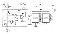
- FIG. 7depicts a quantizing circuit 16 including digital filters 90 that are believed to reduce the likelihood of an erroneous reading.
- the illustrated quantizing circuit 16includes an analog-to-digital converter 88 .
- a digital filter 90 and an analog-to-digital converter 88is coupled to each of the bit-lines 38 , 40 , 42 , 44 , and 46 , respectively. That is, each bit-line 38 , 40 , 42 , 44 , and 46 may connect to a different analog-to-digital converter 88 and digital filter 90 .
- the digital filters 90may connect to an input/output bus 92 , which may connect to a column decoder 18 , a column address latch 20 , and/or control circuitry 28 (see FIG. 2 ).
- the quantizing circuit 16may digitize analog signals from the memory elements 64 in a manner that is relatively robust to noise. As explained below, the quantizing circuit 16 may do this by converting the analog signals into a bit-stream and digitally filtering high-frequency components from the bit-stream with a two-step process.
- the bit-streammay fluctuate between values of zero and one, but its average value, over a sufficiently large period of time, may be proportional to the average value of the analog signal from the memory element 64 .
- the bit-stream from the analog-to-digital converter 88may be a pulse-density modulated (PDM) representation of the analog signal.
- PDMpulse-density modulated
- the analog-to-digital converter 88may transmit the bit-stream to the digital filter 90 on a bit-stream signal path 94 .
- the digital filter 90may remove high-frequency noise from the bit-stream.
- the digital filter 90may be a low-pass filter, such as a circuit configured to calculate an average value of the bit-stream over a sensing time, i.e., the time period over which the memory element 64 is read. As a result, the digital filter 90 may output a value that is representative of both the average value of the bit-stream and the average value of the analog signal from the memory element 64 .
- the digital filter 90includes a counter and a divider, i.e., a circuit configured to perform a division operation on the output of the counter.
- the output from the digital filter 90may be a multi-bit binary signal, e.g., a digital word that is transmitted serially and/or in parallel.
- the quantizing circuit 16may facilitate the use of multi-bit memory elements 64 .
- the number of discrete data values that a memory element 64 storesmay be limited by sense amps that react to noise.
- the quantizing circuit 16may be less susceptible to noise, and, as a result, the memory elements 64 may be configured to store additional data. Without the high frequency noise, the intervals between signals representative of different data values may be made smaller, and the number of data values stored by a given memory element 64 may be increased.
- the quantizing circuit 16may sense memory elements 64 that store several bits of data, e.g., 2, 3, 4, 5, 6, 7, 8, or more bits per memory element 64 .
- the quantizing circuit 16may sample the signal from the memory element 64 over a longer period of time than conventional designs, the overall speed of the memory device 12 may be improved. As compared to a conventional device, each read or write operation of the memory device 12 may transfer more bits of data into or out of the memory element 64 . As a result, while each read or write operation may take longer, more data may be read or written during the operation, thereby improving overall performance. Further, in some memory devices 12 , certain processes may be performed in parallel with a read or write operation, thereby further reducing the overall impact of the longer sensing time. For example, in some embodiments, the memory array 14 may be divided into banks that operate at least partially independently, so that, while data is being written or read from one bank, another bank can read or write data in parallel.
- FIG. 8illustrates details of one implementation of the quantizing circuit 16 .
- the digital filter 90includes a counter 91 and a divider 93
- the analog-to-digital converter 88is a first-order delta-sigma modulator.
- the illustrated delta-sigma modulator 88may include a latched comparator 96 (hereinafter the “comparator”), a capacitor 98 , and a switch 100 .
- the componentshereinafter the “comparator”
- other types of digital filters and analog-to-digital convertersmay be employed.
- an input of the counter 91may connect to the bit-stream signal path 94 , which may connect to an output of the comparator 96 .
- the output of the comparator 96may also connect to a gate of the switch 100 by a feedback signal path 102 .
- the output terminal (e.g., source or drain) of the switch 100may connect in series to one of the bit-lines 38 , 40 , 42 , 44 , or 46 , and the input terminal of the switch 100 may connect to a reference current source 104 (I Ref ).
- One plate of the capacitor 98may connect to one of the bit-lines 38 , 40 , 42 , 44 , or 46 , and the other plate of the capacitor 98 may connect to ground.
- the illustrated counter 91counts the number of clock cycles that the bit-stream 94 is at a logic high value or a logic low value during the sampling period.
- the countermay count up or count down, depending on the embodiment. In some embodiments, the counter 91 may do both, counting up one for each clock cycle that the bit-stream has a logic high value and down one for each clock cycle that the bit-stream has a logic low value.
- Output terminals (D 0 -D 5 ) of the counter 91may connect to the divider 93 , which may include output terminals (D 0 ′-D 4 ′) that connect to the input/output bus 92 for transmitting the average.
- the counter 91may be configured to be reset to zero or some other value when a reset signal is asserted.
- the counter 91may be a series connection of D-flip flops, e.g., D-flip flops having SRAM or other memory for storing an initial value and/or values to be written to the memory element 64 .
- the divider 93may be configured to divide a count from the counter 91 by a divisor to calculate an average.
- the clocked comparator 96compares a reference voltage (V Ref ) to the voltage of one of the bit-lines 38 , 40 , 42 , 44 , or 46 (V BL ), which may be generally equal to the voltage of one plate of the capacitor 98 .
- the comparator 96may be clocked (e.g., falling and/or rising edge triggered), and the comparison may be performed at regular intervals based on the clock signal, e.g., once per clock cycle. Additionally, the comparator 96 may latch, i.e., continue to output, values (V FB ) between comparisons.
- the comparator 96when the clock signals the comparator 96 to perform a comparison, if V BL is less than V Ref , then the comparator 96 may latch its output to a logic low value, as described below with reference to FIG. 9 . Conversely, if V BL is greater than V Ref , then the comparator 96 may latch a logic high value on its output, as described below with reference to FIG. 10 . As a result, the illustrated comparator 96 outputs a bit-stream that indicates whether V BL is larger than V Ref , where the indication is updated once per clock cycle.
- the quantizing circuit 16may include a single comparator (e.g., not more than one) for each column of multi-level memory elements 64 .
- conventional sense amplifiersoften include multiple comparators to read from a multi-bit memory cell, thereby potentially increasing device complexity and cost.
- the capacitor 98may be formed by capacitive coupling of the bit-lines 38 , 40 , 42 , 44 , and 46 . In other designs, this type of capacitance is referred to as parasitic capacitance because it often hinders the operation of the device. However, in this embodiment, the capacitor 98 may be used to integrate differences between currents on the bit-lines 38 , 40 , 42 , 44 , or 46 and the reference current to form the bit-stream, as explained further below. In some embodiments, the capacitor 98 may be supplemented or replaced with an integrated capacitor that provides greater capacitance than the “parasitic” bit-line capacitance.
- the illustrated switch 100selectively transmits current I Ref from the reference current source 104 .
- the switch 100may be a PMOS transistor (as illustrated in FIGS. 8-10 ) or an NMOS transistor (as illustrated in FIG. 17 ) controlled by the V FB signal on the feedback signal path 102 .
- FIGS. 9 and 10depict current flows in the quantizing circuit 16 when the comparator 96 is latched low and high, respectively.
- FIG. 11illustrates V BL , the bit-stream output from the comparator 96 , and the corresponding increasing count of the counter 91 for a relatively small bit-line current.
- FIG. 12depicts the same voltages when measuring a medium sized bit-line current
- FIG. 13depicts these voltages when measuring a relatively large bit-line current.
- the illustrated delta-sigma modulator 88exploits transient effects to generate a bit-stream representative of the bit-line current. Specifically, the delta-sigma modulator 88 may repeatedly charge and discharge the capacitor 98 with a current divider that subtracts the bit-line current from the reference current. Consequently, a large current through the memory element 64 may rapidly discharge the capacitor 98 , and a small current through the memory element 64 may slowly discharge the capacitor 98 .
- the delta-sigma modulator 88switches between two states: the state depicted by FIG. 9 (hereinafter “the charging state”) and the state depicted by FIG. 10 (hereinafter “the discharging state”). Each time the delta-sigma modulator 88 changes between these states, the bit-stream changes from a logic high value to a logic low value or vice versa.
- the proportion of time that the delta-sigma modulator 88 is in the state illustrated by either FIG. 9 or FIG. 10may be proportional to the size of the bit-line current through the memory element 64 . The larger the bit-line current, the more time that the delta-sigma modulator 88 is in the state illustrated by FIG. 9 rather than the state illustrated by FIG. 10 , and the more time that the bit-stream has a logic low value.
- the capacitor 98may initially accumulate a charge.
- the output of the comparator 96is latched to logic low, which, as mentioned above, may occur when V BL is less than V Ref .
- the logic lowmay be conveyed to switch 100 by the feedback signal path 102 , and the switch 100 may close, thereby conducting the reference current, I Ref , through one of the bit-lines 38 , 40 , 42 , 44 , or 46 , as indicated by the larger arrows in FIG. 9 .
- a portion of the electrons flowing through the reference current source 104may be stored by the capacitor 98 , as indicated by the smaller-horizontal arrows, and the remainder may be conducted through the memory element 64 , i.e., the bit-line current, I Bit , as indicated by the smaller vertical arrows.
- the capacitor 98may accumulate a charge, and V BL may increase.
- the comparator 96 and the reference current source 104may cooperate to charge the capacitor 98 for a discrete number of clock cycles. That is, when the delta-sigma modulator 88 enters the charging state, the delta-sigma modulator 88 may remain in this state for an integer number of clock cycles.
- the comparator 96the output of which is latched, changes state no more than once per clock cycle, so the switch 100 , which is controlled by the output of the comparator 96 , V FB , conducts current for a discrete number of clock cycles.
- the reference current source 104conducts current I Ref through the bit-line and into the capacitor 98 for an integer number of clock cycles.
- the delta-sigma modulator 88may transition from the charging state to the discharging state, which is illustrated by FIG. 10 , depending on the relative values of V BL and V Ref .
- the comparator 96may compare the voltage of the capacitor V BL to the reference voltage V Ref . If the capacitor 98 has been charged to the point that V BL is greater than V Ref , then the output of the comparator 96 may transition to logic high, as illustrated in FIG. 10 .
- the logic high signalmay be conveyed to the switch 100 by the feedback signal path 102 , thereby opening the switch 100 .
- the reference current source 104may cease flowing current through the memory element 64 and into the capacitor 98 , and the capacitor 98 may begin to discharge through the memory element 64 .
- V FB0
- the switch 100may close, thereby transitioning the delta-sigma modulator 88 back to the charging state and initiating a new cycle.
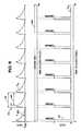
- FIGS. 11-13illustrate voltages V FB and V BL in the quantizing circuit 16 when reading a memory element 64 .
- FIG. 11illustrates a low-current case, in which the value stored by the memory element 64 corresponds to a relatively low bit-line current
- FIG. 12illustrates a medium-current case
- FIG. 13illustrates a high-current case.
- the ordinate of the lower tracerepresents the voltage of the bit-stream signal path 94 , V FB
- the ordinate of the upper traceillustrates the bit-line voltage, I Bit .
- the abscissa in each of the tracesrepresents time, with the lower trace synchronized with the upper trace, and the duration of the time axes is one sensing time 106 .
- the counter 91is initially set to zero (or some other appropriate value, such as one half of the divisor, as explained below) by asserting a reset signal.
- the delta-sigma modulator 88may undergo a number of start-up cycles to reach steady-state operation before initiating the sensing time and resetting the counter 91 .
- the delta-sigma modulator 88is in the charging state, which charges the capacitor 98 and increases V BL , as indicated by dimension arrow 108 .
- the comparator 96compares the bit-line voltage to the reference voltage and determines that the bit-line voltage is greater than the reference voltage.
- the bit-stream signal path 94transitions to a logic high voltage
- the delta-sigma modulator 88transitions to the discharging state.
- the counter 91increments the count by one to account for one clock cycle of the bit-stream signal 94 holding a logic low value.
- the charge stored on the capacitor 98drains out through the memory element 64 , and the bit-line voltage drops until the comparator 96 detects that V BL is less than V Ref , at which point the cycle repeats.
- the cyclehas a period 112 , which may be divided into a charging portion 114 and a discharging portion 116 .
- the count stored in the counter 91may increase by one.
- the counter 91may output the total count.
- FIG. 11A comparison of FIG. 11 to FIGS. 12 and 13 illustrates why the count correlates with the bit-line current.
- FIG. 13the high-current case, the stored charge drains from the capacitor 98 quickly relative to the other cases because the bit-line current is large and, as a result, the delta-sigma modulator 88 spends more time in the charging state than the discharging state. As a result, the bit-stream has a logic low value for a large portion of the sensing time 106 , thereby increasing the count.
- FIG. 14illustrates the generally proportional relationship between the bit-line current and the count.
- the divider 93 in FIG. 15embodies a special case of division in which the dividend is base 2 and the divisor is 2 n , where n is an integer.
- the divider 93may be implemented by dropping less-significant bits of the count.
- the number of less-significant bits that are droppedmay be equal to n.
- the divisoris 1000 in base 2 (i.e., 2 3 or 8 in base 10), so n equals 3 and the 3, least-significant bits are dropped.
- FIG. 16is a graph illustrating the relationship between the input and the output of the divider 93 of FIG. 15 .
- the divider 93 outputis generally equal to the three most-significant bits of the count, and the three least-significant bits of the count are dropped, i.e. not passed on to the input/output bus 92 .
- the illustrated divider 93rounds its output down to the nearest integer. However, in other embodiments, the divider 93 may round its output up to the nearest integer.
- the divisormay have a different value.
- the divisormay be a larger or smaller exponent of the base of the numbering system of the count.
- the divisormay not be an exponent of the base of the numbering system of the count.
- the counter 91may be integrated with the divider 93 , and the counter 91 may increment the count by one for every n clock cycles that the bit-stream is logic high.
- averaging the value of the bit-streamremoves high-frequency noise from the signal.
- the measurements of the bit-line currentare believed to be more accurate, and the memory element 64 may store additional data, in certain embodiments.
- FIG. 16illustrates the relationship between divider output and count for one embodiment.
- the abscissarepresents the count
- the ordinaterepresents the output of the divider.
- the three-least-significant digits of the countare disregarded as noise. That is, D 0 -D 2 ( FIG. 8 ) either do not connect to the input/output bus 92 or are not interpreted as conveying data stored by the memory element 64 .
- a range of counter valuesmay represent a single data value stored by the memory device 64 . For example, in the present embodiment, counter values ranging from 001 000 to 001 111 are construed as representing a data value of 001.
- Representing data in this manneris believed to further reduce the effects of noise because, even if noise affects the count, in many embodiments, it would have to affect the count in a consistent manner over a long period of time to affect the more significant digits of the count. That is, disregarding less significant digits is believed to lower the cutoff frequency of the counter 90 . In other embodiments, fewer, more, or no digits may be truncated from the count as potentially representing noise.
- FIG. 17depicts an example of a read operation 118 that is performed by certain embodiments of the quantizing circuit 16 .
- the read operation 118begins with presetting the counter, as illustrated by block 120 .
- the counteris preset to one-half of the divisor to average out the effect of the divider rounding down to the nearest integer.
- the countmay be preset to negative-one-half of the divisor.
- the countermay be set to zero.
- the reference currentis conducted both into the capacitor and through the memory cell, as illustrated by block 122 . Then, a determination is made as to whether a new clock cycle has started, as depicted by block 124 . Depending on the result, the read operation 118 either returns to block 122 or continues to block 126 , where a determination is made as to whether the voltage of the capacitor is greater than a reference voltage. Depending on the result, the read operation 118 either returns to block 122 or continues to block 128 , at which point the reference current is no longer conducted. Next, the capacitor is discharged through the memory element, as depicted by block 130 , and a determination is made as to whether a new clock cycle has started, as depicted by block 134 .
- the capacitorcontinues to discharge through the memory cell, as described by block 130 , or the count is increased by one, as depicted by block 136 . Then, a determination is made as to whether the voltage of the capacitor is less than the reference voltage, as depicted by block 138 . Based on the result of the determination, the read operation 118 either returns to block 130 to continue discharging the capacitor or continues to block 140 , where a determination is made as to whether the sensing time has elapsed. Based on the determination at block 140 , the read operation 118 either returns to block 122 to initiate a new charge and discharge cycle or outputs a count from the counter to the divider, as depicted by block 142 .
- the dividermay then divide the count by the divisor, as illustrated by block 143 . In certain cases, this step may be performed by dropping less significant bits from the count.
- the average valueis output, as illustrated by block 144 . Outputting the average value may include storing the average value in memory, transmitting the average value to another component, displaying the average value, or using the average value in subsequent calculations.
- FIG. 18illustrates an exemplary write operation 146 .
- the illustrated write operation 146begins with erasing the memory element, as illustrated by block 148 .
- a block or cell of memory elementsmay be erased generally simultaneously.
- a memory-element property that is used to store datais adjusted by one increment, as illustrated by block 150 .
- Adjusting a memory-element propertymay include driving a charge on to a floating gate or partially changing the phase of a phase-change memory element.
- the memory elementis read, as illustrated by block 152 . This step may include performing the read operation 118 illustrated in FIG. 17 .
- the memory elementAfter reading the memory element, it is determined whether the value stored by the memory element is generally equal to the target value to be written to the memory element, as illustrated by block 154 . If the value to be written is not generally equal to the value to be stored, then the memory element property may be adjusted by another increment, and the operation 146 may return to block 150 . On the other hand, if the value stored by the memory element is generally equal to the target value, then the write operation 146 may end, as illustrated by block 156 .
- FIG. 19depicts an exemplary processor-based system 310 that includes the memory device 12 .
- the system 310may include the imaging device 13 .
- the system 310may be any of a variety of types such as a computer, pager, cellular phone, personal organizer, control circuit, etc.
- processors 312such as a microprocessor, control the processing of system functions and requests in the system 310 .
- the processor 312 and other subcomponents of the system 310may include quantizing circuits, such as those discussed above.
- the system 310typically includes a power supply 314 .
- the power supply 314may advantageously include a fuel cell, permanent batteries, replaceable batteries, and/or rechargeable batteries.
- the power supply 314may also include an AC adapter, so the system 310 may be plugged into a wall outlet, for instance.
- the power supply 314may also include a DC adapter such that the system 310 may be plugged into a vehicle cigarette lighter, for instance.
- a user interface 316may be coupled to the processor 312 .
- the user interface 316may include buttons, switches, a keyboard, a light pen, a mouse, a digitizer and stylus, and/or a voice recognition system, for instance.
- a display 318may also be coupled to the processor 312 .
- the display 318may include an LCD, an SED display, a CRT display, a DLP display, a plasma display, an OLED display, LEDs, and/or an audio display, for example.
- an RF sub-system/baseband processor 320may also be coupled to the processor 312 .
- the RF sub-system/baseband processor 320may include an antenna that is coupled to an RF receiver and to an RF transmitter (not shown).
- One or more communication ports 322may also be coupled to the processor 312 .
- the communication port 322may be adapted to be coupled to one or more peripheral devices 324 such as a modem, a printer, a computer, or to a network, such as a local area network, remote area network, intranet, or the Internet, for instance.
- the processor 312generally controls the system 310 by implementing software programs stored in the memory.
- the memoryis operably coupled to the processor 312 to store and facilitate execution of various programs.
- the processor 312may be coupled to the volatile memory 326 which may include Dynamic Random Access Memory (DRAM) and/or Static Random Access Memory (SRAM).
- DRAMDynamic Random Access Memory
- SRAMStatic Random Access Memory
- the volatile memory 326is typically large so that it can store dynamically loaded applications and data. As described further below, the volatile memory 326 may be configured in accordance with embodiments of the present invention.
- the processor 312may also be coupled to the memory device 12 .
- the memory device 12may include a read-only memory (ROM), such as an EPROM, and/or flash memory to be used in conjunction with the volatile memory 326 .
- ROMread-only memory
- the size of the ROMis typically selected to be just large enough to store any necessary operating system, application programs, and fixed data.
- the non-volatile memory 328may include a high capacity memory such as a tape or disk drive memory.
- the memory device 10 and volatile memory 326may store various types of software, such as an operating system or office productivity suite including a word processing application, a spreadsheet application, an email application, and/or a database application.
- an operating system or office productivity suiteincluding a word processing application, a spreadsheet application, an email application, and/or a database application.
Landscapes
- Engineering & Computer Science (AREA)
- Computer Hardware Design (AREA)
- Microelectronics & Electronic Packaging (AREA)
- Chemical & Material Sciences (AREA)
- Crystallography & Structural Chemistry (AREA)
- Analogue/Digital Conversion (AREA)
- Compression, Expansion, Code Conversion, And Decoders (AREA)
- Semiconductor Memories (AREA)
Abstract
Description
Claims (26)
Priority Applications (4)
| Application Number | Priority Date | Filing Date | Title |
|---|---|---|---|
| US11/820,007US7768868B2 (en) | 2007-06-15 | 2007-06-15 | Digital filters for semiconductor devices |
| PCT/US2008/065403WO2008156999A1 (en) | 2007-06-15 | 2008-05-30 | Digital filters for semiconductor devices |
| TW097121937ATWI389134B (en) | 2007-06-15 | 2008-06-12 | Digital filters for semiconductor devices |
| US12/829,251US8149646B2 (en) | 2007-06-15 | 2010-07-01 | Digital filters for semiconductor devices |
Applications Claiming Priority (1)
| Application Number | Priority Date | Filing Date | Title |
|---|---|---|---|
| US11/820,007US7768868B2 (en) | 2007-06-15 | 2007-06-15 | Digital filters for semiconductor devices |
Related Child Applications (1)
| Application Number | Title | Priority Date | Filing Date |
|---|---|---|---|
| US12/829,251ContinuationUS8149646B2 (en) | 2007-06-15 | 2010-07-01 | Digital filters for semiconductor devices |
Publications (2)
| Publication Number | Publication Date |
|---|---|
| US20080310245A1 US20080310245A1 (en) | 2008-12-18 |
| US7768868B2true US7768868B2 (en) | 2010-08-03 |
Family
ID=39734127
Family Applications (2)
| Application Number | Title | Priority Date | Filing Date |
|---|---|---|---|
| US11/820,007Active2028-06-11US7768868B2 (en) | 2007-06-15 | 2007-06-15 | Digital filters for semiconductor devices |
| US12/829,251ActiveUS8149646B2 (en) | 2007-06-15 | 2010-07-01 | Digital filters for semiconductor devices |
Family Applications After (1)
| Application Number | Title | Priority Date | Filing Date |
|---|---|---|---|
| US12/829,251ActiveUS8149646B2 (en) | 2007-06-15 | 2010-07-01 | Digital filters for semiconductor devices |
Country Status (3)
| Country | Link |
|---|---|
| US (2) | US7768868B2 (en) |
| TW (1) | TWI389134B (en) |
| WO (1) | WO2008156999A1 (en) |
Cited By (4)
| Publication number | Priority date | Publication date | Assignee | Title |
|---|---|---|---|---|
| US20110051511A1 (en)* | 2007-06-15 | 2011-03-03 | Micron Technology, Inc. | Digital filters with memory |
| US20110063930A1 (en)* | 2007-06-15 | 2011-03-17 | Micron Technology, Inc. | Subtraction circuits and digital-to-analog converters for semiconductor devices |
| US20140177319A1 (en)* | 2012-12-21 | 2014-06-26 | SK Hynix Inc. | Nonvolatile memory apparatus |
| US9336084B2 (en) | 2007-06-15 | 2016-05-10 | Micron Technology, Inc. | Error detection for multi-bit memory |
Families Citing this family (6)
| Publication number | Priority date | Publication date | Assignee | Title |
|---|---|---|---|---|
| US8542521B2 (en)* | 2011-09-12 | 2013-09-24 | Kabushiki Kaisha Toshiba | Semiconductor storage device including memory cells capable of holding data |
| US11144824B2 (en)* | 2019-01-29 | 2021-10-12 | Silicon Storage Technology, Inc. | Algorithms and circuitry for verifying a value stored during a programming operation of a non-volatile memory cell in an analog neural memory in deep learning artificial neural network |
| US12353503B2 (en)* | 2019-05-02 | 2025-07-08 | Silicon Storage Technology, Inc. | Output array neuron conversion and calibration for analog neural memory in deep learning artificial neural network |
| CN111404517B (en)* | 2020-04-08 | 2023-11-10 | 北京集创北方科技股份有限公司 | Pulse cancellation circuit, voltage detection circuit, and detection method |
| TWI750841B (en)* | 2020-10-12 | 2021-12-21 | 茂達電子股份有限公司 | High linearity digital controlling light sensor and method |
| TWI789188B (en) | 2021-12-29 | 2023-01-01 | 悅視界有限公司 | Filter system and operation method thereof |
Citations (36)
| Publication number | Priority date | Publication date | Assignee | Title |
|---|---|---|---|---|
| US5600319A (en) | 1994-11-01 | 1997-02-04 | Ylsi Technology, Inc. | Thermometric-to-digital-to-analog converter occupying reduced chip area |
| US5614856A (en) | 1996-03-11 | 1997-03-25 | Micron Technology, Inc. | Waveshaping circuit generating two rising slopes for a sense amplifier pulldown device |
| US5953276A (en) | 1997-12-18 | 1999-09-14 | Micron Technology, Inc. | Fully-differential amplifier |
| US6044019A (en) | 1998-10-23 | 2000-03-28 | Sandisk Corporation | Non-volatile memory with improved sensing and method therefor |
| US6188340B1 (en) | 1997-08-10 | 2001-02-13 | Hitachi, Ltd. | Sensor adjusting circuit |
| US20020101758A1 (en) | 2001-02-01 | 2002-08-01 | Baker R. Jacob | Design methodology for sensing resistance values of memory cells |
| US6490200B2 (en) | 2000-03-27 | 2002-12-03 | Sandisk Corporation | Non-volatile memory with improved sensing and method therefor |
| US20020194557A1 (en) | 2001-06-19 | 2002-12-19 | Samsung Electronics Co., Ltd. | Built-in self test circuit using linear feedback shift register |
| US6504750B1 (en) | 2001-08-27 | 2003-01-07 | Micron Technology, Inc. | Resistive memory element sensing using averaging |
| US20030007413A1 (en)* | 2001-06-13 | 2003-01-09 | Seiko Epson Corporation | Semiconductor memory and burn-in method for the same |
| US20030039162A1 (en) | 2001-08-27 | 2003-02-27 | Baker R. Jacob | Offset compensated sensing for magnetic random access memory |
| US20030043616A1 (en) | 2001-08-28 | 2003-03-06 | Baker R. J. | Sensing method and apparatus for resistance memory device |
| US20030214868A1 (en) | 2002-05-16 | 2003-11-20 | Baker R. Jacob | Noise resistant small signal sensing circuit for a memory device |
| US6664708B2 (en) | 1998-12-23 | 2003-12-16 | Voltage Vision Ltd. | Method and device for non-contact detection of external electric or magnetic fields |
| US6665013B1 (en) | 1994-01-28 | 2003-12-16 | California Institute Of Technology | Active pixel sensor having intra-pixel charge transfer with analog-to-digital converter |
| US20040008555A1 (en) | 2002-07-09 | 2004-01-15 | Baker R. Jacob | System and method for sensing data stored in a resistive memory element using one bit of a digital count |
| US20040032760A1 (en) | 2002-08-19 | 2004-02-19 | Baker R. Jacob | Dual loop sensing scheme for resistive memory elements |
| US6741502B1 (en) | 2001-09-17 | 2004-05-25 | Sandisk Corporation | Background operation for memory cells |
| US6781906B2 (en) | 2002-11-19 | 2004-08-24 | Hewlett-Packard Development Company, L.P. | Memory cell sensing integrator |
| US6795359B1 (en) | 2003-06-10 | 2004-09-21 | Micron Technology, Inc. | Methods and apparatus for measuring current as in sensing a memory cell |
| US20040190334A1 (en) | 2003-03-28 | 2004-09-30 | Baker R. J. | Method for reducing power consumption when sensing a resistive memory |
| US6807403B2 (en) | 1998-04-03 | 2004-10-19 | Nec Corporation | Radio telephone apparatus |
| US20040240294A1 (en) | 2003-05-28 | 2004-12-02 | Baker R. Jacob | Integrated charge sensing scheme for resistive memories |
| US6847234B2 (en) | 2000-12-07 | 2005-01-25 | Hynix Semiconductor Inc. | Comparison apparatus operated at a low voltage |
| US6850441B2 (en) | 2002-01-18 | 2005-02-01 | Sandisk Corporation | Noise reduction technique for transistors and small devices utilizing an episodic agitation |
| US20050041128A1 (en) | 2003-08-22 | 2005-02-24 | Baker R. Jacob | Per column one-bit ADC for image sensors |
| US6977601B1 (en) | 2004-01-29 | 2005-12-20 | Raytheon Company | Low power current input delta-sigma ADC using injection FET reference |
| US6985375B2 (en) | 2003-06-11 | 2006-01-10 | Micron Technology, Inc. | Adjusting the frequency of an oscillator for use in a resistive sense amp |
| US20060030277A1 (en)* | 2004-02-10 | 2006-02-09 | Cyr Russell J | Programmable radio transceiver |
| US7002833B2 (en) | 2001-11-20 | 2006-02-21 | Micron Technology, Inc. | Complementary bit resistance memory sensor and method of operation |
| US7102932B2 (en) | 2004-08-27 | 2006-09-05 | Micron Technology, Inc. | Input and output buffers having symmetrical operating characteristics and immunity from voltage variations |
| US20060221696A1 (en) | 2005-04-01 | 2006-10-05 | Yan Li | Method for Non-Volatile Memory with Background Data Latch Caching During Read Operations |
| US20060250853A1 (en) | 2005-05-04 | 2006-11-09 | Jennifer Taylor | Method and apparatus for sensing flash memory using delta sigma modulation |
| US7142475B2 (en)* | 1997-10-10 | 2006-11-28 | Rambus, Inc. | Memory device having a configurable oscillator for refresh operation |
| US20060291291A1 (en) | 2005-06-22 | 2006-12-28 | Kabushiki Kaisha Toshiba | Non-volatile semiconductor memory device |
| US20080309530A1 (en) | 2007-06-15 | 2008-12-18 | Baker R Jacob | Quantizing circuits with variable parameters |
Family Cites Families (5)
| Publication number | Priority date | Publication date | Assignee | Title |
|---|---|---|---|---|
| US5680336A (en)* | 1994-04-19 | 1997-10-21 | Northrop Grumman Corporation | Continuous wave synthesis from a finite periodic waveform |
| US6795395B1 (en)* | 1999-09-17 | 2004-09-21 | Verizon Laboratories Inc. | Automation of call setup in IP telephony for tests and measurements |
| JP2002319111A (en)* | 2001-02-15 | 2002-10-31 | Fujitsu Ltd | Magnetoresistive magnetic head |
| JP2005049970A (en)* | 2003-07-30 | 2005-02-24 | Renesas Technology Corp | Semiconductor integrated circuit |
| TWI242852B (en)* | 2004-05-05 | 2005-11-01 | Orient Semiconductor Elect Ltd | Semiconductor package |
- 2007
- 2007-06-15USUS11/820,007patent/US7768868B2/enactiveActive
- 2008
- 2008-05-30WOPCT/US2008/065403patent/WO2008156999A1/enactiveApplication Filing
- 2008-06-12TWTW097121937Apatent/TWI389134B/enactive
- 2010
- 2010-07-01USUS12/829,251patent/US8149646B2/enactiveActive
Patent Citations (75)
| Publication number | Priority date | Publication date | Assignee | Title |
|---|---|---|---|---|
| US6665013B1 (en) | 1994-01-28 | 2003-12-16 | California Institute Of Technology | Active pixel sensor having intra-pixel charge transfer with analog-to-digital converter |
| US5600319A (en) | 1994-11-01 | 1997-02-04 | Ylsi Technology, Inc. | Thermometric-to-digital-to-analog converter occupying reduced chip area |
| US5614856A (en) | 1996-03-11 | 1997-03-25 | Micron Technology, Inc. | Waveshaping circuit generating two rising slopes for a sense amplifier pulldown device |
| US6188340B1 (en) | 1997-08-10 | 2001-02-13 | Hitachi, Ltd. | Sensor adjusting circuit |
| US7142475B2 (en)* | 1997-10-10 | 2006-11-28 | Rambus, Inc. | Memory device having a configurable oscillator for refresh operation |
| US5953276A (en) | 1997-12-18 | 1999-09-14 | Micron Technology, Inc. | Fully-differential amplifier |
| US6807403B2 (en) | 1998-04-03 | 2004-10-19 | Nec Corporation | Radio telephone apparatus |
| US6661708B2 (en) | 1998-10-23 | 2003-12-09 | Sandisk Corporation | Non-volatile memory with improved sensing and method therefor |
| US6282120B1 (en) | 1998-10-23 | 2001-08-28 | Sandisk Corporation | Non-volatile memory with improved sensing and method therefor |
| US6044019A (en) | 1998-10-23 | 2000-03-28 | Sandisk Corporation | Non-volatile memory with improved sensing and method therefor |
| US6664708B2 (en) | 1998-12-23 | 2003-12-16 | Voltage Vision Ltd. | Method and device for non-contact detection of external electric or magnetic fields |
| US6490200B2 (en) | 2000-03-27 | 2002-12-03 | Sandisk Corporation | Non-volatile memory with improved sensing and method therefor |
| US6847234B2 (en) | 2000-12-07 | 2005-01-25 | Hynix Semiconductor Inc. | Comparison apparatus operated at a low voltage |
| US20020101758A1 (en) | 2001-02-01 | 2002-08-01 | Baker R. Jacob | Design methodology for sensing resistance values of memory cells |
| US6785156B2 (en) | 2001-02-01 | 2004-08-31 | Micron Technology, Inc. | Method and apparatus for sensing resistance values of memory cells |
| US6567297B2 (en) | 2001-02-01 | 2003-05-20 | Micron Technology, Inc. | Method and apparatus for sensing resistance values of memory cells |
| US20030007413A1 (en)* | 2001-06-13 | 2003-01-09 | Seiko Epson Corporation | Semiconductor memory and burn-in method for the same |
| US20020194557A1 (en) | 2001-06-19 | 2002-12-19 | Samsung Electronics Co., Ltd. | Built-in self test circuit using linear feedback shift register |
| US20030067797A1 (en) | 2001-08-27 | 2003-04-10 | Baker R. J. | Resistive memory element sensing using averaging |
| US7133307B2 (en) | 2001-08-27 | 2006-11-07 | Micron Technology, Inc. | Resistive memory element sensing using averaging |
| US20040062100A1 (en) | 2001-08-27 | 2004-04-01 | R. J. Baker | Resistive memory element sensing using averaging |
| US20050201145A1 (en) | 2001-08-27 | 2005-09-15 | R. J. Baker | Resistive memory element sensing using averaging |
| US20040199710A1 (en) | 2001-08-27 | 2004-10-07 | Baker R. J. | Offset compensated sensing for magnetic random access memory |
| US20030039162A1 (en) | 2001-08-27 | 2003-02-27 | Baker R. Jacob | Offset compensated sensing for magnetic random access memory |
| US6504750B1 (en) | 2001-08-27 | 2003-01-07 | Micron Technology, Inc. | Resistive memory element sensing using averaging |
| US6822892B2 (en) | 2001-08-27 | 2004-11-23 | Micron Technology, Inc. | Resistive memory element sensing using averaging |
| US20040190327A1 (en) | 2001-08-28 | 2004-09-30 | Baker R. J. | Sensing method and apparatus for resistance memory device |
| US20030198078A1 (en) | 2001-08-28 | 2003-10-23 | Baker R. J. | Sensing method and apparatus for resistance memory device |
| US20030043616A1 (en) | 2001-08-28 | 2003-03-06 | Baker R. J. | Sensing method and apparatus for resistance memory device |
| US6741502B1 (en) | 2001-09-17 | 2004-05-25 | Sandisk Corporation | Background operation for memory cells |
| US7002833B2 (en) | 2001-11-20 | 2006-02-21 | Micron Technology, Inc. | Complementary bit resistance memory sensor and method of operation |
| US6850441B2 (en) | 2002-01-18 | 2005-02-01 | Sandisk Corporation | Noise reduction technique for transistors and small devices utilizing an episodic agitation |
| US6826102B2 (en) | 2002-05-16 | 2004-11-30 | Micron Technology, Inc. | Noise resistant small signal sensing circuit for a memory device |
| US20040076052A1 (en) | 2002-05-16 | 2004-04-22 | Baker R. Jacob | Noise resistant small signal sensing circuit for a memory device |
| US20050088892A1 (en) | 2002-05-16 | 2005-04-28 | Baker R. J. | Noise resistant small signal sensing circuit for a memory device |
| US6798705B2 (en) | 2002-05-16 | 2004-09-28 | Micron Technology, Inc. | Noise resistant small signal sensing circuit for a memory device |
| US20030214868A1 (en) | 2002-05-16 | 2003-11-20 | Baker R. Jacob | Noise resistant small signal sensing circuit for a memory device |
| US6856564B2 (en) | 2002-05-16 | 2005-02-15 | Micron Technology, Inc. | Noise resistant small signal sensing circuit for a memory device |
| US20060227641A1 (en) | 2002-05-16 | 2006-10-12 | Baker R J | Noise resistant small signal sensing circuit for a memory device |
| US7095667B2 (en) | 2002-05-16 | 2006-08-22 | Micron Technology, Inc. | Noise resistant small signal sensing circuit for a memory device |
| US20050007803A1 (en) | 2002-05-16 | 2005-01-13 | Baker R. Jacob | Noise resistant small signal sensing circuit for a memory device |
| US20050007850A1 (en) | 2002-05-16 | 2005-01-13 | Baker R. Jacob | Noise resistant small signal sensing circuit for a memory device |
| US20050088893A1 (en) | 2002-05-16 | 2005-04-28 | Baker R. J. | Noise resistant small signal sensing circuit for a memory device |
| US6954391B2 (en) | 2002-05-16 | 2005-10-11 | Micron Technology, Inc. | Noise resistant small signal sensing circuit for a memory device |
| US6954390B2 (en) | 2002-05-16 | 2005-10-11 | Micron Technology, Inc. | Noise resistant small signal sensing circuit for a memory device |
| US7009901B2 (en) | 2002-07-09 | 2006-03-07 | Micron Technology, Inc. | System and method for sensing data stored in a resistive memory element using one bit of a digital count |
| US20040095839A1 (en) | 2002-07-09 | 2004-05-20 | Baker R. Jacob | System and method for sensing data stored in a resistive memory element using one bit of a digital count |
| US20040008555A1 (en) | 2002-07-09 | 2004-01-15 | Baker R. Jacob | System and method for sensing data stored in a resistive memory element using one bit of a digital count |
| US6813208B2 (en) | 2002-07-09 | 2004-11-02 | Micron Technology, Inc. | System and method for sensing data stored in a resistive memory element using one bit of a digital count |
| US6914838B2 (en) | 2002-08-19 | 2005-07-05 | Micron Technology, Inc. | Dual loop sensing scheme for resistive memory elements |
| US6829188B2 (en) | 2002-08-19 | 2004-12-07 | Micron Technology, Inc. | Dual loop sensing scheme for resistive memory elements |
| US20050013184A1 (en) | 2002-08-19 | 2005-01-20 | Baker R. Jacob | Dual loop sensing scheme for resistive memory elements |
| US20040032760A1 (en) | 2002-08-19 | 2004-02-19 | Baker R. Jacob | Dual loop sensing scheme for resistive memory elements |
| US6781906B2 (en) | 2002-11-19 | 2004-08-24 | Hewlett-Packard Development Company, L.P. | Memory cell sensing integrator |
| US20050018477A1 (en) | 2003-03-28 | 2005-01-27 | R. J. Baker | Method and apparatus sensing a resistive memory with reduced power consumption |
| US20040190334A1 (en) | 2003-03-28 | 2004-09-30 | Baker R. J. | Method for reducing power consumption when sensing a resistive memory |
| US6901020B2 (en) | 2003-05-28 | 2005-05-31 | Micron Technology, Inc. | Integrated charge sensing scheme for resistive memories |
| US20050018512A1 (en) | 2003-05-28 | 2005-01-27 | Baker R. Jacob | Integrated charge sensing scheme for resistive memories |
| US20040240294A1 (en) | 2003-05-28 | 2004-12-02 | Baker R. Jacob | Integrated charge sensing scheme for resistive memories |
| US6870784B2 (en) | 2003-05-28 | 2005-03-22 | Micron Technology, Inc. | Integrated charge sensing scheme for resistive memories |
| US20060062062A1 (en) | 2003-05-28 | 2006-03-23 | Baker R J | Integrated charge sensing scheme for resistive memories |
| US6795359B1 (en) | 2003-06-10 | 2004-09-21 | Micron Technology, Inc. | Methods and apparatus for measuring current as in sensing a memory cell |
| US6930942B2 (en) | 2003-06-10 | 2005-08-16 | Micron Technology, Inc. | Method and apparatus for measuring current as in sensing a memory cell |
| US20050002249A1 (en) | 2003-06-10 | 2005-01-06 | Baker R. Jacob | Method and apparatus for measuring current as in sensing a memory cell |
| US6985375B2 (en) | 2003-06-11 | 2006-01-10 | Micron Technology, Inc. | Adjusting the frequency of an oscillator for use in a resistive sense amp |
| US20060013040A1 (en) | 2003-06-11 | 2006-01-19 | Baker R J | Adjusting the frequency of an oscillator for use in a resistive sense amp |
| US20050041128A1 (en) | 2003-08-22 | 2005-02-24 | Baker R. Jacob | Per column one-bit ADC for image sensors |
| US6977601B1 (en) | 2004-01-29 | 2005-12-20 | Raytheon Company | Low power current input delta-sigma ADC using injection FET reference |
| US20060030277A1 (en)* | 2004-02-10 | 2006-02-09 | Cyr Russell J | Programmable radio transceiver |
| US7102932B2 (en) | 2004-08-27 | 2006-09-05 | Micron Technology, Inc. | Input and output buffers having symmetrical operating characteristics and immunity from voltage variations |
| US20060221696A1 (en) | 2005-04-01 | 2006-10-05 | Yan Li | Method for Non-Volatile Memory with Background Data Latch Caching During Read Operations |
| US20060250853A1 (en) | 2005-05-04 | 2006-11-09 | Jennifer Taylor | Method and apparatus for sensing flash memory using delta sigma modulation |
| US7366021B2 (en) | 2005-05-04 | 2008-04-29 | Micron Technology, Inc. | Method and apparatus for sensing flash memory using delta sigma modulation |
| US20060291291A1 (en) | 2005-06-22 | 2006-12-28 | Kabushiki Kaisha Toshiba | Non-volatile semiconductor memory device |
| US20080309530A1 (en) | 2007-06-15 | 2008-12-18 | Baker R Jacob | Quantizing circuits with variable parameters |
Non-Patent Citations (17)
| Title |
|---|
| Baker, "CMOS Circuit Design, Layout, and Simulation," Second Edition, IEEE Press, A. John Wiley & Sons, Inc.; Copyright 2005; Chapters 13, 16, 17, 20, 22-24, 28-29; pp. 375-396, 433-522, 613-656, 711-828, 931-1022. |
| Baker, "CMOS Mixed Signal Circuit Design," IEEE Press, A. John Wiley & Sons, Inc.; Copyright 2003, Figures 30.63, 31.82, 32.6, 32.7, 32.24, 32.51, 33.34, 33.47, 33.51, 34.18, 34.24; located at http://cmosedu.com/cmos2/book2.htm. |
| Baker, R.J. (2004) Delta-Sigma Modulation for Sensing, IEEE/EDS Workshop on Microelectronics and Electron Devices (WMED), Apr. 2004. |
| Baker, R.J. (2005) Design of High-Speed CMOS Op-Amps for Signal Processing, IEEE/EDS Workshop on Microelectronics and Electron Devices (WMED), Apr. 2005. |
| Baker, R.J. and Saxena, V., (2007) Design of Bandpass Delta Sigma Modulators: Avoiding Common Mistakes, presented at various universities and companies. |
| Baker, R.J., (2001-2006) Sensing Circuits for Resistive Memory, presented at various universities and companies. |
| Baker, R.J., (2003) Mixed-Signal Design in the Microelectronics Curriculum, IEEE University/Government/Industry Microelectronics (UGIM) Symposium, Jun. 30-Jul. 2, 2003. |
| Dallas Semiconductor, Maxim Application Note 1870, "Demystifying Sigma-Delta ADCs," (Jan. 31, 2003), 15 pgs. |
| Duvvada, K., Saxena, V., and Baker, R. J., (2006) High Speed Digital Input Buffer Circuits, proceedings of the IEEE/EDS Workshop on Microelectronics and Electron Devices (WMED), pp. 11-12, Apr. 2006. |
| Hadrick, M. and Baker, R.J., (2005) Sensing in CMOS Imagers using Delta-Sigma Modulation, a general presentation of our work in this area. |
| Leslie, M.B., and Baker, R.J., (2006) "Noise-Shaping Sense Amplifier for MRAM Cross-Point Arrays," IEEE Journal of Solid State Circuits, vol. 41, No. 3, pp. 699-704. |
| Park, "Motorola Digital Signal Processors-Principles of Sigma-Delta Modulation for Analog-to-Digital Converters," (Undated). |
| Rane Corporation, RaneNote 137, "Digital Charma of Audio A/D Converters," 1997, 12 pgs. |
| Saxena, V., Plum, T.J., Jessing, J.R., and Baker, R. J., (2006) Design and Fabrication of a MEMS Capacitive Chemical Sensor System, proceedings of the IEEE/EDS Workshop on Microelectronics and Electron Devices (WMED), pp. 17-18, Ap. 2006. |
| Wikipedia-definition of "Error detection and correction", pulled from website Jun. 1, 2007, 9 pgs. |
| Wikipedia-definition of "Hamming code", pulled from website Jun. 1, 2007, 8 pgs. |
| Wikipedia-definition of "Linear feedback shift register (LFSR)," pulled from website Jun. 1, 2007, 4 pgs. |
Cited By (15)
| Publication number | Priority date | Publication date | Assignee | Title |
|---|---|---|---|---|
| US9070469B2 (en) | 2007-06-15 | 2015-06-30 | Micron Technology, Inc. | Digital filters with memory |
| US9299405B2 (en) | 2007-06-15 | 2016-03-29 | Micron Technology, Inc. | Methods for sensing memory elements in semiconductor devices |
| US8194477B2 (en) | 2007-06-15 | 2012-06-05 | Micron Technology, Inc. | Subtraction circuits and digital-to-analog converters for semiconductor devices |
| US8582375B2 (en) | 2007-06-15 | 2013-11-12 | Micron Technology, Inc. | Methods for sensing memory elements in semiconductor devices |
| US10658018B2 (en) | 2007-06-15 | 2020-05-19 | Micron Technology, Inc. | Quantizing circuits having improved sensing |
| US8854899B2 (en) | 2007-06-15 | 2014-10-07 | Micron Technology, Inc. | Methods for sensing memory elements in semiconductor devices |
| US20110063930A1 (en)* | 2007-06-15 | 2011-03-17 | Micron Technology, Inc. | Subtraction circuits and digital-to-analog converters for semiconductor devices |
| US9734894B2 (en) | 2007-06-15 | 2017-08-15 | Micron Technology, Inc. | Digital filters with memory |
| US20110051511A1 (en)* | 2007-06-15 | 2011-03-03 | Micron Technology, Inc. | Digital filters with memory |
| US9449664B2 (en) | 2007-06-15 | 2016-09-20 | Micron Technology, Inc. | Quantizing circuits having improved sensing |
| US9336084B2 (en) | 2007-06-15 | 2016-05-10 | Micron Technology, Inc. | Error detection for multi-bit memory |
| US10127954B2 (en) | 2007-06-15 | 2018-11-13 | Micron Technology, Inc. | Quantizing circuits having improved sensing |
| US10366744B2 (en) | 2007-06-15 | 2019-07-30 | Micron Technology, Inc. | Digital filters with memory |
| US10403339B2 (en) | 2007-06-15 | 2019-09-03 | Micron Technology, Inc. | Quantizing circuits having improved sensing |
| US20140177319A1 (en)* | 2012-12-21 | 2014-06-26 | SK Hynix Inc. | Nonvolatile memory apparatus |
Also Published As
| Publication number | Publication date |
|---|---|
| US8149646B2 (en) | 2012-04-03 |
| US20100271899A1 (en) | 2010-10-28 |
| WO2008156999A1 (en) | 2008-12-24 |
| US20080310245A1 (en) | 2008-12-18 |
| TW200908001A (en) | 2009-02-16 |
| TWI389134B (en) | 2013-03-11 |
Similar Documents
| Publication | Publication Date | Title |
|---|---|---|
| US10658018B2 (en) | Quantizing circuits having improved sensing | |
| US10366744B2 (en) | Digital filters with memory | |
| US7538702B2 (en) | Quantizing circuits with variable parameters | |
| US8717220B2 (en) | Methods of quantizing signals using variable reference signals | |
| US8149646B2 (en) | Digital filters for semiconductor devices | |
| US8754795B2 (en) | Integrators for delta-sigma modulators | |
| US8098180B2 (en) | Devices including analog-to-digital converters for internal data storage locations |
Legal Events
| Date | Code | Title | Description |
|---|---|---|---|
| AS | Assignment | Owner name:MICRON TECHNOLOGY, INC., IDAHO Free format text:ASSIGNMENT OF ASSIGNORS INTEREST;ASSIGNOR:BAKER, R. JACOB;REEL/FRAME:019502/0907 Effective date:20070403 | |
| FEPP | Fee payment procedure | Free format text:PAYOR NUMBER ASSIGNED (ORIGINAL EVENT CODE: ASPN); ENTITY STATUS OF PATENT OWNER: LARGE ENTITY | |
| STCF | Information on status: patent grant | Free format text:PATENTED CASE | |
| FPAY | Fee payment | Year of fee payment:4 | |
| AS | Assignment | Owner name:U.S. BANK NATIONAL ASSOCIATION, AS COLLATERAL AGENT, CALIFORNIA Free format text:SECURITY INTEREST;ASSIGNOR:MICRON TECHNOLOGY, INC.;REEL/FRAME:038669/0001 Effective date:20160426 Owner name:U.S. BANK NATIONAL ASSOCIATION, AS COLLATERAL AGEN Free format text:SECURITY INTEREST;ASSIGNOR:MICRON TECHNOLOGY, INC.;REEL/FRAME:038669/0001 Effective date:20160426 | |
| AS | Assignment | Owner name:MORGAN STANLEY SENIOR FUNDING, INC., AS COLLATERAL AGENT, MARYLAND Free format text:PATENT SECURITY AGREEMENT;ASSIGNOR:MICRON TECHNOLOGY, INC.;REEL/FRAME:038954/0001 Effective date:20160426 Owner name:MORGAN STANLEY SENIOR FUNDING, INC., AS COLLATERAL Free format text:PATENT SECURITY AGREEMENT;ASSIGNOR:MICRON TECHNOLOGY, INC.;REEL/FRAME:038954/0001 Effective date:20160426 | |
| AS | Assignment | Owner name:U.S. BANK NATIONAL ASSOCIATION, AS COLLATERAL AGENT, CALIFORNIA Free format text:CORRECTIVE ASSIGNMENT TO CORRECT THE REPLACE ERRONEOUSLY FILED PATENT #7358718 WITH THE CORRECT PATENT #7358178 PREVIOUSLY RECORDED ON REEL 038669 FRAME 0001. ASSIGNOR(S) HEREBY CONFIRMS THE SECURITY INTEREST;ASSIGNOR:MICRON TECHNOLOGY, INC.;REEL/FRAME:043079/0001 Effective date:20160426 Owner name:U.S. BANK NATIONAL ASSOCIATION, AS COLLATERAL AGEN Free format text:CORRECTIVE ASSIGNMENT TO CORRECT THE REPLACE ERRONEOUSLY FILED PATENT #7358718 WITH THE CORRECT PATENT #7358178 PREVIOUSLY RECORDED ON REEL 038669 FRAME 0001. ASSIGNOR(S) HEREBY CONFIRMS THE SECURITY INTEREST;ASSIGNOR:MICRON TECHNOLOGY, INC.;REEL/FRAME:043079/0001 Effective date:20160426 | |
| MAFP | Maintenance fee payment | Free format text:PAYMENT OF MAINTENANCE FEE, 8TH YEAR, LARGE ENTITY (ORIGINAL EVENT CODE: M1552) Year of fee payment:8 | |
| AS | Assignment | Owner name:JPMORGAN CHASE BANK, N.A., AS COLLATERAL AGENT, ILLINOIS Free format text:SECURITY INTEREST;ASSIGNORS:MICRON TECHNOLOGY, INC.;MICRON SEMICONDUCTOR PRODUCTS, INC.;REEL/FRAME:047540/0001 Effective date:20180703 Owner name:JPMORGAN CHASE BANK, N.A., AS COLLATERAL AGENT, IL Free format text:SECURITY INTEREST;ASSIGNORS:MICRON TECHNOLOGY, INC.;MICRON SEMICONDUCTOR PRODUCTS, INC.;REEL/FRAME:047540/0001 Effective date:20180703 | |
| AS | Assignment | Owner name:MICRON TECHNOLOGY, INC., IDAHO Free format text:RELEASE BY SECURED PARTY;ASSIGNOR:U.S. BANK NATIONAL ASSOCIATION, AS COLLATERAL AGENT;REEL/FRAME:047243/0001 Effective date:20180629 | |
| AS | Assignment | Owner name:MICRON TECHNOLOGY, INC., IDAHO Free format text:RELEASE BY SECURED PARTY;ASSIGNOR:MORGAN STANLEY SENIOR FUNDING, INC., AS COLLATERAL AGENT;REEL/FRAME:050937/0001 Effective date:20190731 | |
| AS | Assignment | Owner name:MICRON TECHNOLOGY, INC., IDAHO Free format text:RELEASE BY SECURED PARTY;ASSIGNOR:JPMORGAN CHASE BANK, N.A., AS COLLATERAL AGENT;REEL/FRAME:051028/0001 Effective date:20190731 Owner name:MICRON SEMICONDUCTOR PRODUCTS, INC., IDAHO Free format text:RELEASE BY SECURED PARTY;ASSIGNOR:JPMORGAN CHASE BANK, N.A., AS COLLATERAL AGENT;REEL/FRAME:051028/0001 Effective date:20190731 | |
| MAFP | Maintenance fee payment | Free format text:PAYMENT OF MAINTENANCE FEE, 12TH YEAR, LARGE ENTITY (ORIGINAL EVENT CODE: M1553); ENTITY STATUS OF PATENT OWNER: LARGE ENTITY Year of fee payment:12 |