US7768125B2 - Multi-chip package system - Google Patents
Multi-chip package systemDownload PDFInfo
- Publication number
- US7768125B2 US7768125B2US11/326,211US32621106AUS7768125B2US 7768125 B2US7768125 B2US 7768125B2US 32621106 AUS32621106 AUS 32621106AUS 7768125 B2US7768125 B2US 7768125B2
- Authority
- US
- United States
- Prior art keywords
- interconnects
- chip
- molding compound
- wafer
- package
- Prior art date
- Legal status (The legal status is an assumption and is not a legal conclusion. Google has not performed a legal analysis and makes no representation as to the accuracy of the status listed.)
- Active, expires
Links
Images


Classifications
- H—ELECTRICITY
- H01—ELECTRIC ELEMENTS
- H01L—SEMICONDUCTOR DEVICES NOT COVERED BY CLASS H10
- H01L25/00—Assemblies consisting of a plurality of semiconductor or other solid state devices
- H01L25/16—Assemblies consisting of a plurality of semiconductor or other solid state devices the devices being of types provided for in two or more different subclasses of H10B, H10D, H10F, H10H, H10K or H10N, e.g. forming hybrid circuits
- H—ELECTRICITY
- H01—ELECTRIC ELEMENTS
- H01L—SEMICONDUCTOR DEVICES NOT COVERED BY CLASS H10
- H01L21/00—Processes or apparatus adapted for the manufacture or treatment of semiconductor or solid state devices or of parts thereof
- H01L21/67—Apparatus specially adapted for handling semiconductor or electric solid state devices during manufacture or treatment thereof; Apparatus specially adapted for handling wafers during manufacture or treatment of semiconductor or electric solid state devices or components ; Apparatus not specifically provided for elsewhere
- H01L21/683—Apparatus specially adapted for handling semiconductor or electric solid state devices during manufacture or treatment thereof; Apparatus specially adapted for handling wafers during manufacture or treatment of semiconductor or electric solid state devices or components ; Apparatus not specifically provided for elsewhere for supporting or gripping
- H01L21/6835—Apparatus specially adapted for handling semiconductor or electric solid state devices during manufacture or treatment thereof; Apparatus specially adapted for handling wafers during manufacture or treatment of semiconductor or electric solid state devices or components ; Apparatus not specifically provided for elsewhere for supporting or gripping using temporarily an auxiliary support
- H01L21/6836—Wafer tapes, e.g. grinding or dicing support tapes
- H—ELECTRICITY
- H01—ELECTRIC ELEMENTS
- H01L—SEMICONDUCTOR DEVICES NOT COVERED BY CLASS H10
- H01L21/00—Processes or apparatus adapted for the manufacture or treatment of semiconductor or solid state devices or of parts thereof
- H01L21/70—Manufacture or treatment of devices consisting of a plurality of solid state components formed in or on a common substrate or of parts thereof; Manufacture of integrated circuit devices or of parts thereof
- H01L21/77—Manufacture or treatment of devices consisting of a plurality of solid state components or integrated circuits formed in, or on, a common substrate
- H01L21/78—Manufacture or treatment of devices consisting of a plurality of solid state components or integrated circuits formed in, or on, a common substrate with subsequent division of the substrate into plural individual devices
- H—ELECTRICITY
- H01—ELECTRIC ELEMENTS
- H01L—SEMICONDUCTOR DEVICES NOT COVERED BY CLASS H10
- H01L23/00—Details of semiconductor or other solid state devices
- H01L23/28—Encapsulations, e.g. encapsulating layers, coatings, e.g. for protection
- H01L23/31—Encapsulations, e.g. encapsulating layers, coatings, e.g. for protection characterised by the arrangement or shape
- H01L23/3107—Encapsulations, e.g. encapsulating layers, coatings, e.g. for protection characterised by the arrangement or shape the device being completely enclosed
- H01L23/3114—Encapsulations, e.g. encapsulating layers, coatings, e.g. for protection characterised by the arrangement or shape the device being completely enclosed the device being a chip scale package, e.g. CSP
- H—ELECTRICITY
- H01—ELECTRIC ELEMENTS
- H01L—SEMICONDUCTOR DEVICES NOT COVERED BY CLASS H10
- H01L23/00—Details of semiconductor or other solid state devices
- H01L23/48—Arrangements for conducting electric current to or from the solid state body in operation, e.g. leads, terminal arrangements ; Selection of materials therefor
- H01L23/488—Arrangements for conducting electric current to or from the solid state body in operation, e.g. leads, terminal arrangements ; Selection of materials therefor consisting of soldered or bonded constructions
- H01L23/498—Leads, i.e. metallisations or lead-frames on insulating substrates, e.g. chip carriers
- H01L23/49811—Additional leads joined to the metallisation on the insulating substrate, e.g. pins, bumps, wires, flat leads
- H01L23/49816—Spherical bumps on the substrate for external connection, e.g. ball grid arrays [BGA]
- H—ELECTRICITY
- H01—ELECTRIC ELEMENTS
- H01L—SEMICONDUCTOR DEVICES NOT COVERED BY CLASS H10
- H01L24/00—Arrangements for connecting or disconnecting semiconductor or solid-state bodies; Methods or apparatus related thereto
- H01L24/01—Means for bonding being attached to, or being formed on, the surface to be connected, e.g. chip-to-package, die-attach, "first-level" interconnects; Manufacturing methods related thereto
- H01L24/02—Bonding areas ; Manufacturing methods related thereto
- H01L24/04—Structure, shape, material or disposition of the bonding areas prior to the connecting process
- H01L24/05—Structure, shape, material or disposition of the bonding areas prior to the connecting process of an individual bonding area
- H—ELECTRICITY
- H01—ELECTRIC ELEMENTS
- H01L—SEMICONDUCTOR DEVICES NOT COVERED BY CLASS H10
- H01L24/00—Arrangements for connecting or disconnecting semiconductor or solid-state bodies; Methods or apparatus related thereto
- H01L24/01—Means for bonding being attached to, or being formed on, the surface to be connected, e.g. chip-to-package, die-attach, "first-level" interconnects; Manufacturing methods related thereto
- H01L24/10—Bump connectors ; Manufacturing methods related thereto
- H01L24/11—Manufacturing methods
- H—ELECTRICITY
- H01—ELECTRIC ELEMENTS
- H01L—SEMICONDUCTOR DEVICES NOT COVERED BY CLASS H10
- H01L24/00—Arrangements for connecting or disconnecting semiconductor or solid-state bodies; Methods or apparatus related thereto
- H01L24/01—Means for bonding being attached to, or being formed on, the surface to be connected, e.g. chip-to-package, die-attach, "first-level" interconnects; Manufacturing methods related thereto
- H01L24/10—Bump connectors ; Manufacturing methods related thereto
- H01L24/12—Structure, shape, material or disposition of the bump connectors prior to the connecting process
- H—ELECTRICITY
- H01—ELECTRIC ELEMENTS
- H01L—SEMICONDUCTOR DEVICES NOT COVERED BY CLASS H10
- H01L24/00—Arrangements for connecting or disconnecting semiconductor or solid-state bodies; Methods or apparatus related thereto
- H01L24/01—Means for bonding being attached to, or being formed on, the surface to be connected, e.g. chip-to-package, die-attach, "first-level" interconnects; Manufacturing methods related thereto
- H01L24/10—Bump connectors ; Manufacturing methods related thereto
- H01L24/15—Structure, shape, material or disposition of the bump connectors after the connecting process
- H01L24/17—Structure, shape, material or disposition of the bump connectors after the connecting process of a plurality of bump connectors
- H—ELECTRICITY
- H01—ELECTRIC ELEMENTS
- H01L—SEMICONDUCTOR DEVICES NOT COVERED BY CLASS H10
- H01L24/00—Arrangements for connecting or disconnecting semiconductor or solid-state bodies; Methods or apparatus related thereto
- H01L24/01—Means for bonding being attached to, or being formed on, the surface to be connected, e.g. chip-to-package, die-attach, "first-level" interconnects; Manufacturing methods related thereto
- H01L24/26—Layer connectors, e.g. plate connectors, solder or adhesive layers; Manufacturing methods related thereto
- H01L24/27—Manufacturing methods
- H—ELECTRICITY
- H01—ELECTRIC ELEMENTS
- H01L—SEMICONDUCTOR DEVICES NOT COVERED BY CLASS H10
- H01L24/00—Arrangements for connecting or disconnecting semiconductor or solid-state bodies; Methods or apparatus related thereto
- H01L24/01—Means for bonding being attached to, or being formed on, the surface to be connected, e.g. chip-to-package, die-attach, "first-level" interconnects; Manufacturing methods related thereto
- H01L24/42—Wire connectors; Manufacturing methods related thereto
- H01L24/47—Structure, shape, material or disposition of the wire connectors after the connecting process
- H01L24/48—Structure, shape, material or disposition of the wire connectors after the connecting process of an individual wire connector
- H—ELECTRICITY
- H01—ELECTRIC ELEMENTS
- H01L—SEMICONDUCTOR DEVICES NOT COVERED BY CLASS H10
- H01L24/00—Arrangements for connecting or disconnecting semiconductor or solid-state bodies; Methods or apparatus related thereto
- H01L24/73—Means for bonding being of different types provided for in two or more of groups H01L24/10, H01L24/18, H01L24/26, H01L24/34, H01L24/42, H01L24/50, H01L24/63, H01L24/71
- H—ELECTRICITY
- H01—ELECTRIC ELEMENTS
- H01L—SEMICONDUCTOR DEVICES NOT COVERED BY CLASS H10
- H01L24/00—Arrangements for connecting or disconnecting semiconductor or solid-state bodies; Methods or apparatus related thereto
- H01L24/91—Methods for connecting semiconductor or solid state bodies including different methods provided for in two or more of groups H01L24/80 - H01L24/90
- H—ELECTRICITY
- H01—ELECTRIC ELEMENTS
- H01L—SEMICONDUCTOR DEVICES NOT COVERED BY CLASS H10
- H01L24/00—Arrangements for connecting or disconnecting semiconductor or solid-state bodies; Methods or apparatus related thereto
- H01L24/93—Batch processes
- H01L24/94—Batch processes at wafer-level, i.e. with connecting carried out on a wafer comprising a plurality of undiced individual devices
- H—ELECTRICITY
- H01—ELECTRIC ELEMENTS
- H01L—SEMICONDUCTOR DEVICES NOT COVERED BY CLASS H10
- H01L25/00—Assemblies consisting of a plurality of semiconductor or other solid state devices
- H01L25/03—Assemblies consisting of a plurality of semiconductor or other solid state devices all the devices being of a type provided for in a single subclass of subclasses H10B, H10D, H10F, H10H, H10K or H10N, e.g. assemblies of rectifier diodes
- H01L25/04—Assemblies consisting of a plurality of semiconductor or other solid state devices all the devices being of a type provided for in a single subclass of subclasses H10B, H10D, H10F, H10H, H10K or H10N, e.g. assemblies of rectifier diodes the devices not having separate containers
- H01L25/065—Assemblies consisting of a plurality of semiconductor or other solid state devices all the devices being of a type provided for in a single subclass of subclasses H10B, H10D, H10F, H10H, H10K or H10N, e.g. assemblies of rectifier diodes the devices not having separate containers the devices being of a type provided for in group H10D89/00
- H01L25/0652—Assemblies consisting of a plurality of semiconductor or other solid state devices all the devices being of a type provided for in a single subclass of subclasses H10B, H10D, H10F, H10H, H10K or H10N, e.g. assemblies of rectifier diodes the devices not having separate containers the devices being of a type provided for in group H10D89/00 the devices being arranged next and on each other, i.e. mixed assemblies
- H—ELECTRICITY
- H01—ELECTRIC ELEMENTS
- H01L—SEMICONDUCTOR DEVICES NOT COVERED BY CLASS H10
- H01L25/00—Assemblies consisting of a plurality of semiconductor or other solid state devices
- H01L25/03—Assemblies consisting of a plurality of semiconductor or other solid state devices all the devices being of a type provided for in a single subclass of subclasses H10B, H10D, H10F, H10H, H10K or H10N, e.g. assemblies of rectifier diodes
- H01L25/10—Assemblies consisting of a plurality of semiconductor or other solid state devices all the devices being of a type provided for in a single subclass of subclasses H10B, H10D, H10F, H10H, H10K or H10N, e.g. assemblies of rectifier diodes the devices having separate containers
- H01L25/105—Assemblies consisting of a plurality of semiconductor or other solid state devices all the devices being of a type provided for in a single subclass of subclasses H10B, H10D, H10F, H10H, H10K or H10N, e.g. assemblies of rectifier diodes the devices having separate containers the devices being integrated devices of class H10
- H—ELECTRICITY
- H01—ELECTRIC ELEMENTS
- H01L—SEMICONDUCTOR DEVICES NOT COVERED BY CLASS H10
- H01L2221/00—Processes or apparatus adapted for the manufacture or treatment of semiconductor or solid state devices or of parts thereof covered by H01L21/00
- H01L2221/67—Apparatus for handling semiconductor or electric solid state devices during manufacture or treatment thereof; Apparatus for handling wafers during manufacture or treatment of semiconductor or electric solid state devices or components; Apparatus not specifically provided for elsewhere
- H01L2221/683—Apparatus for handling semiconductor or electric solid state devices during manufacture or treatment thereof; Apparatus for handling wafers during manufacture or treatment of semiconductor or electric solid state devices or components; Apparatus not specifically provided for elsewhere for supporting or gripping
- H01L2221/68304—Apparatus for handling semiconductor or electric solid state devices during manufacture or treatment thereof; Apparatus for handling wafers during manufacture or treatment of semiconductor or electric solid state devices or components; Apparatus not specifically provided for elsewhere for supporting or gripping using temporarily an auxiliary support
- H01L2221/68327—Apparatus for handling semiconductor or electric solid state devices during manufacture or treatment thereof; Apparatus for handling wafers during manufacture or treatment of semiconductor or electric solid state devices or components; Apparatus not specifically provided for elsewhere for supporting or gripping using temporarily an auxiliary support used during dicing or grinding
- H—ELECTRICITY
- H01—ELECTRIC ELEMENTS
- H01L—SEMICONDUCTOR DEVICES NOT COVERED BY CLASS H10
- H01L2224/00—Indexing scheme for arrangements for connecting or disconnecting semiconductor or solid-state bodies and methods related thereto as covered by H01L24/00
- H01L2224/01—Means for bonding being attached to, or being formed on, the surface to be connected, e.g. chip-to-package, die-attach, "first-level" interconnects; Manufacturing methods related thereto
- H01L2224/02—Bonding areas; Manufacturing methods related thereto
- H01L2224/04—Structure, shape, material or disposition of the bonding areas prior to the connecting process
- H01L2224/0401—Bonding areas specifically adapted for bump connectors, e.g. under bump metallisation [UBM]
- H—ELECTRICITY
- H01—ELECTRIC ELEMENTS
- H01L—SEMICONDUCTOR DEVICES NOT COVERED BY CLASS H10
- H01L2224/00—Indexing scheme for arrangements for connecting or disconnecting semiconductor or solid-state bodies and methods related thereto as covered by H01L24/00
- H01L2224/01—Means for bonding being attached to, or being formed on, the surface to be connected, e.g. chip-to-package, die-attach, "first-level" interconnects; Manufacturing methods related thereto
- H01L2224/02—Bonding areas; Manufacturing methods related thereto
- H01L2224/04—Structure, shape, material or disposition of the bonding areas prior to the connecting process
- H01L2224/04042—Bonding areas specifically adapted for wire connectors, e.g. wirebond pads
- H—ELECTRICITY
- H01—ELECTRIC ELEMENTS
- H01L—SEMICONDUCTOR DEVICES NOT COVERED BY CLASS H10
- H01L2224/00—Indexing scheme for arrangements for connecting or disconnecting semiconductor or solid-state bodies and methods related thereto as covered by H01L24/00
- H01L2224/01—Means for bonding being attached to, or being formed on, the surface to be connected, e.g. chip-to-package, die-attach, "first-level" interconnects; Manufacturing methods related thereto
- H01L2224/02—Bonding areas; Manufacturing methods related thereto
- H01L2224/04—Structure, shape, material or disposition of the bonding areas prior to the connecting process
- H01L2224/04073—Bonding areas specifically adapted for connectors of different types
- H—ELECTRICITY
- H01—ELECTRIC ELEMENTS
- H01L—SEMICONDUCTOR DEVICES NOT COVERED BY CLASS H10
- H01L2224/00—Indexing scheme for arrangements for connecting or disconnecting semiconductor or solid-state bodies and methods related thereto as covered by H01L24/00
- H01L2224/01—Means for bonding being attached to, or being formed on, the surface to be connected, e.g. chip-to-package, die-attach, "first-level" interconnects; Manufacturing methods related thereto
- H01L2224/02—Bonding areas; Manufacturing methods related thereto
- H01L2224/04—Structure, shape, material or disposition of the bonding areas prior to the connecting process
- H01L2224/05—Structure, shape, material or disposition of the bonding areas prior to the connecting process of an individual bonding area
- H01L2224/0554—External layer
- H01L2224/0555—Shape
- H01L2224/05556—Shape in side view
- H—ELECTRICITY
- H01—ELECTRIC ELEMENTS
- H01L—SEMICONDUCTOR DEVICES NOT COVERED BY CLASS H10
- H01L2224/00—Indexing scheme for arrangements for connecting or disconnecting semiconductor or solid-state bodies and methods related thereto as covered by H01L24/00
- H01L2224/01—Means for bonding being attached to, or being formed on, the surface to be connected, e.g. chip-to-package, die-attach, "first-level" interconnects; Manufacturing methods related thereto
- H01L2224/02—Bonding areas; Manufacturing methods related thereto
- H01L2224/04—Structure, shape, material or disposition of the bonding areas prior to the connecting process
- H01L2224/05—Structure, shape, material or disposition of the bonding areas prior to the connecting process of an individual bonding area
- H01L2224/0554—External layer
- H01L2224/05599—Material
- H—ELECTRICITY
- H01—ELECTRIC ELEMENTS
- H01L—SEMICONDUCTOR DEVICES NOT COVERED BY CLASS H10
- H01L2224/00—Indexing scheme for arrangements for connecting or disconnecting semiconductor or solid-state bodies and methods related thereto as covered by H01L24/00
- H01L2224/01—Means for bonding being attached to, or being formed on, the surface to be connected, e.g. chip-to-package, die-attach, "first-level" interconnects; Manufacturing methods related thereto
- H01L2224/02—Bonding areas; Manufacturing methods related thereto
- H01L2224/04—Structure, shape, material or disposition of the bonding areas prior to the connecting process
- H01L2224/06—Structure, shape, material or disposition of the bonding areas prior to the connecting process of a plurality of bonding areas
- H01L2224/0601—Structure
- H01L2224/0603—Bonding areas having different sizes, e.g. different heights or widths
- H—ELECTRICITY
- H01—ELECTRIC ELEMENTS
- H01L—SEMICONDUCTOR DEVICES NOT COVERED BY CLASS H10
- H01L2224/00—Indexing scheme for arrangements for connecting or disconnecting semiconductor or solid-state bodies and methods related thereto as covered by H01L24/00
- H01L2224/01—Means for bonding being attached to, or being formed on, the surface to be connected, e.g. chip-to-package, die-attach, "first-level" interconnects; Manufacturing methods related thereto
- H01L2224/10—Bump connectors; Manufacturing methods related thereto
- H01L2224/11—Manufacturing methods
- H01L2224/118—Post-treatment of the bump connector
- H01L2224/1183—Reworking, e.g. shaping
- H01L2224/1184—Reworking, e.g. shaping involving a mechanical process, e.g. planarising the bump connector
- H—ELECTRICITY
- H01—ELECTRIC ELEMENTS
- H01L—SEMICONDUCTOR DEVICES NOT COVERED BY CLASS H10
- H01L2224/00—Indexing scheme for arrangements for connecting or disconnecting semiconductor or solid-state bodies and methods related thereto as covered by H01L24/00
- H01L2224/01—Means for bonding being attached to, or being formed on, the surface to be connected, e.g. chip-to-package, die-attach, "first-level" interconnects; Manufacturing methods related thereto
- H01L2224/10—Bump connectors; Manufacturing methods related thereto
- H01L2224/11—Manufacturing methods
- H01L2224/119—Methods of manufacturing bump connectors involving a specific sequence of method steps
- H01L2224/11901—Methods of manufacturing bump connectors involving a specific sequence of method steps with repetition of the same manufacturing step
- H—ELECTRICITY
- H01—ELECTRIC ELEMENTS
- H01L—SEMICONDUCTOR DEVICES NOT COVERED BY CLASS H10
- H01L2224/00—Indexing scheme for arrangements for connecting or disconnecting semiconductor or solid-state bodies and methods related thereto as covered by H01L24/00
- H01L2224/01—Means for bonding being attached to, or being formed on, the surface to be connected, e.g. chip-to-package, die-attach, "first-level" interconnects; Manufacturing methods related thereto
- H01L2224/10—Bump connectors; Manufacturing methods related thereto
- H01L2224/12—Structure, shape, material or disposition of the bump connectors prior to the connecting process
- H01L2224/13—Structure, shape, material or disposition of the bump connectors prior to the connecting process of an individual bump connector
- H01L2224/13001—Core members of the bump connector
- H01L2224/1302—Disposition
- H01L2224/13022—Disposition the bump connector being at least partially embedded in the surface
- H—ELECTRICITY
- H01—ELECTRIC ELEMENTS
- H01L—SEMICONDUCTOR DEVICES NOT COVERED BY CLASS H10
- H01L2224/00—Indexing scheme for arrangements for connecting or disconnecting semiconductor or solid-state bodies and methods related thereto as covered by H01L24/00
- H01L2224/01—Means for bonding being attached to, or being formed on, the surface to be connected, e.g. chip-to-package, die-attach, "first-level" interconnects; Manufacturing methods related thereto
- H01L2224/10—Bump connectors; Manufacturing methods related thereto
- H01L2224/12—Structure, shape, material or disposition of the bump connectors prior to the connecting process
- H01L2224/13—Structure, shape, material or disposition of the bump connectors prior to the connecting process of an individual bump connector
- H01L2224/13001—Core members of the bump connector
- H01L2224/13099—Material
- H01L2224/131—Material with a principal constituent of the material being a metal or a metalloid, e.g. boron [B], silicon [Si], germanium [Ge], arsenic [As], antimony [Sb], tellurium [Te] and polonium [Po], and alloys thereof
- H—ELECTRICITY
- H01—ELECTRIC ELEMENTS
- H01L—SEMICONDUCTOR DEVICES NOT COVERED BY CLASS H10
- H01L2224/00—Indexing scheme for arrangements for connecting or disconnecting semiconductor or solid-state bodies and methods related thereto as covered by H01L24/00
- H01L2224/01—Means for bonding being attached to, or being formed on, the surface to be connected, e.g. chip-to-package, die-attach, "first-level" interconnects; Manufacturing methods related thereto
- H01L2224/10—Bump connectors; Manufacturing methods related thereto
- H01L2224/12—Structure, shape, material or disposition of the bump connectors prior to the connecting process
- H01L2224/14—Structure, shape, material or disposition of the bump connectors prior to the connecting process of a plurality of bump connectors
- H01L2224/1401—Structure
- H01L2224/1403—Bump connectors having different sizes, e.g. different diameters, heights or widths
- H—ELECTRICITY
- H01—ELECTRIC ELEMENTS
- H01L—SEMICONDUCTOR DEVICES NOT COVERED BY CLASS H10
- H01L2224/00—Indexing scheme for arrangements for connecting or disconnecting semiconductor or solid-state bodies and methods related thereto as covered by H01L24/00
- H01L2224/01—Means for bonding being attached to, or being formed on, the surface to be connected, e.g. chip-to-package, die-attach, "first-level" interconnects; Manufacturing methods related thereto
- H01L2224/10—Bump connectors; Manufacturing methods related thereto
- H01L2224/15—Structure, shape, material or disposition of the bump connectors after the connecting process
- H01L2224/16—Structure, shape, material or disposition of the bump connectors after the connecting process of an individual bump connector
- H01L2224/161—Disposition
- H01L2224/16135—Disposition the bump connector connecting between different semiconductor or solid-state bodies, i.e. chip-to-chip
- H01L2224/16145—Disposition the bump connector connecting between different semiconductor or solid-state bodies, i.e. chip-to-chip the bodies being stacked
- H—ELECTRICITY
- H01—ELECTRIC ELEMENTS
- H01L—SEMICONDUCTOR DEVICES NOT COVERED BY CLASS H10
- H01L2224/00—Indexing scheme for arrangements for connecting or disconnecting semiconductor or solid-state bodies and methods related thereto as covered by H01L24/00
- H01L2224/01—Means for bonding being attached to, or being formed on, the surface to be connected, e.g. chip-to-package, die-attach, "first-level" interconnects; Manufacturing methods related thereto
- H01L2224/26—Layer connectors, e.g. plate connectors, solder or adhesive layers; Manufacturing methods related thereto
- H01L2224/27—Manufacturing methods
- H01L2224/274—Manufacturing methods by blanket deposition of the material of the layer connector
- H—ELECTRICITY
- H01—ELECTRIC ELEMENTS
- H01L—SEMICONDUCTOR DEVICES NOT COVERED BY CLASS H10
- H01L2224/00—Indexing scheme for arrangements for connecting or disconnecting semiconductor or solid-state bodies and methods related thereto as covered by H01L24/00
- H01L2224/01—Means for bonding being attached to, or being formed on, the surface to be connected, e.g. chip-to-package, die-attach, "first-level" interconnects; Manufacturing methods related thereto
- H01L2224/42—Wire connectors; Manufacturing methods related thereto
- H01L2224/47—Structure, shape, material or disposition of the wire connectors after the connecting process
- H01L2224/48—Structure, shape, material or disposition of the wire connectors after the connecting process of an individual wire connector
- H01L2224/4805—Shape
- H01L2224/4809—Loop shape
- H01L2224/48091—Arched
- H—ELECTRICITY
- H01—ELECTRIC ELEMENTS
- H01L—SEMICONDUCTOR DEVICES NOT COVERED BY CLASS H10
- H01L2224/00—Indexing scheme for arrangements for connecting or disconnecting semiconductor or solid-state bodies and methods related thereto as covered by H01L24/00
- H01L2224/01—Means for bonding being attached to, or being formed on, the surface to be connected, e.g. chip-to-package, die-attach, "first-level" interconnects; Manufacturing methods related thereto
- H01L2224/42—Wire connectors; Manufacturing methods related thereto
- H01L2224/47—Structure, shape, material or disposition of the wire connectors after the connecting process
- H01L2224/48—Structure, shape, material or disposition of the wire connectors after the connecting process of an individual wire connector
- H01L2224/481—Disposition
- H01L2224/48151—Connecting between a semiconductor or solid-state body and an item not being a semiconductor or solid-state body, e.g. chip-to-substrate, chip-to-passive
- H01L2224/48221—Connecting between a semiconductor or solid-state body and an item not being a semiconductor or solid-state body, e.g. chip-to-substrate, chip-to-passive the body and the item being stacked
- H01L2224/48225—Connecting between a semiconductor or solid-state body and an item not being a semiconductor or solid-state body, e.g. chip-to-substrate, chip-to-passive the body and the item being stacked the item being non-metallic, e.g. insulating substrate with or without metallisation
- H01L2224/48227—Connecting between a semiconductor or solid-state body and an item not being a semiconductor or solid-state body, e.g. chip-to-substrate, chip-to-passive the body and the item being stacked the item being non-metallic, e.g. insulating substrate with or without metallisation connecting the wire to a bond pad of the item
- H—ELECTRICITY
- H01—ELECTRIC ELEMENTS
- H01L—SEMICONDUCTOR DEVICES NOT COVERED BY CLASS H10
- H01L2224/00—Indexing scheme for arrangements for connecting or disconnecting semiconductor or solid-state bodies and methods related thereto as covered by H01L24/00
- H01L2224/01—Means for bonding being attached to, or being formed on, the surface to be connected, e.g. chip-to-package, die-attach, "first-level" interconnects; Manufacturing methods related thereto
- H01L2224/42—Wire connectors; Manufacturing methods related thereto
- H01L2224/47—Structure, shape, material or disposition of the wire connectors after the connecting process
- H01L2224/48—Structure, shape, material or disposition of the wire connectors after the connecting process of an individual wire connector
- H01L2224/484—Connecting portions
- H01L2224/48463—Connecting portions the connecting portion on the bonding area of the semiconductor or solid-state body being a ball bond
- H01L2224/48465—Connecting portions the connecting portion on the bonding area of the semiconductor or solid-state body being a ball bond the other connecting portion not on the bonding area being a wedge bond, i.e. ball-to-wedge, regular stitch
- H—ELECTRICITY
- H01—ELECTRIC ELEMENTS
- H01L—SEMICONDUCTOR DEVICES NOT COVERED BY CLASS H10
- H01L2224/00—Indexing scheme for arrangements for connecting or disconnecting semiconductor or solid-state bodies and methods related thereto as covered by H01L24/00
- H01L2224/01—Means for bonding being attached to, or being formed on, the surface to be connected, e.g. chip-to-package, die-attach, "first-level" interconnects; Manufacturing methods related thereto
- H01L2224/42—Wire connectors; Manufacturing methods related thereto
- H01L2224/47—Structure, shape, material or disposition of the wire connectors after the connecting process
- H01L2224/48—Structure, shape, material or disposition of the wire connectors after the connecting process of an individual wire connector
- H01L2224/484—Connecting portions
- H01L2224/48475—Connecting portions connected to auxiliary connecting means on the bonding areas, e.g. pre-ball, wedge-on-ball, ball-on-ball
- H—ELECTRICITY
- H01—ELECTRIC ELEMENTS
- H01L—SEMICONDUCTOR DEVICES NOT COVERED BY CLASS H10
- H01L2224/00—Indexing scheme for arrangements for connecting or disconnecting semiconductor or solid-state bodies and methods related thereto as covered by H01L24/00
- H01L2224/73—Means for bonding being of different types provided for in two or more of groups H01L2224/10, H01L2224/18, H01L2224/26, H01L2224/34, H01L2224/42, H01L2224/50, H01L2224/63, H01L2224/71
- H01L2224/732—Location after the connecting process
- H01L2224/73251—Location after the connecting process on different surfaces
- H01L2224/73253—Bump and layer connectors
- H—ELECTRICITY
- H01—ELECTRIC ELEMENTS
- H01L—SEMICONDUCTOR DEVICES NOT COVERED BY CLASS H10
- H01L2224/00—Indexing scheme for arrangements for connecting or disconnecting semiconductor or solid-state bodies and methods related thereto as covered by H01L24/00
- H01L2224/73—Means for bonding being of different types provided for in two or more of groups H01L2224/10, H01L2224/18, H01L2224/26, H01L2224/34, H01L2224/42, H01L2224/50, H01L2224/63, H01L2224/71
- H01L2224/732—Location after the connecting process
- H01L2224/73251—Location after the connecting process on different surfaces
- H01L2224/73265—Layer and wire connectors
- H—ELECTRICITY
- H01—ELECTRIC ELEMENTS
- H01L—SEMICONDUCTOR DEVICES NOT COVERED BY CLASS H10
- H01L2224/00—Indexing scheme for arrangements for connecting or disconnecting semiconductor or solid-state bodies and methods related thereto as covered by H01L24/00
- H01L2224/80—Methods for connecting semiconductor or other solid state bodies using means for bonding being attached to, or being formed on, the surface to be connected
- H01L2224/83—Methods for connecting semiconductor or other solid state bodies using means for bonding being attached to, or being formed on, the surface to be connected using a layer connector
- H01L2224/831—Methods for connecting semiconductor or other solid state bodies using means for bonding being attached to, or being formed on, the surface to be connected using a layer connector the layer connector being supplied to the parts to be connected in the bonding apparatus
- H01L2224/83101—Methods for connecting semiconductor or other solid state bodies using means for bonding being attached to, or being formed on, the surface to be connected using a layer connector the layer connector being supplied to the parts to be connected in the bonding apparatus as prepeg comprising a layer connector, e.g. provided in an insulating plate member
- H—ELECTRICITY
- H01—ELECTRIC ELEMENTS
- H01L—SEMICONDUCTOR DEVICES NOT COVERED BY CLASS H10
- H01L2224/00—Indexing scheme for arrangements for connecting or disconnecting semiconductor or solid-state bodies and methods related thereto as covered by H01L24/00
- H01L2224/80—Methods for connecting semiconductor or other solid state bodies using means for bonding being attached to, or being formed on, the surface to be connected
- H01L2224/85—Methods for connecting semiconductor or other solid state bodies using means for bonding being attached to, or being formed on, the surface to be connected using a wire connector
- H01L2224/8538—Bonding interfaces outside the semiconductor or solid-state body
- H01L2224/85399—Material
- H—ELECTRICITY
- H01—ELECTRIC ELEMENTS
- H01L—SEMICONDUCTOR DEVICES NOT COVERED BY CLASS H10
- H01L2225/00—Details relating to assemblies covered by the group H01L25/00 but not provided for in its subgroups
- H01L2225/03—All the devices being of a type provided for in the same main group of the same subclass of class H10, e.g. assemblies of rectifier diodes
- H01L2225/10—All the devices being of a type provided for in the same main group of the same subclass of class H10, e.g. assemblies of rectifier diodes the devices having separate containers
- H01L2225/1005—All the devices being of a type provided for in the same main group of the same subclass of class H10, e.g. assemblies of rectifier diodes the devices having separate containers the devices being integrated devices of class H10
- H01L2225/1011—All the devices being of a type provided for in the same main group of the same subclass of class H10, e.g. assemblies of rectifier diodes the devices having separate containers the devices being integrated devices of class H10 the containers being in a stacked arrangement
- H01L2225/1017—All the devices being of a type provided for in the same main group of the same subclass of class H10, e.g. assemblies of rectifier diodes the devices having separate containers the devices being integrated devices of class H10 the containers being in a stacked arrangement the lowermost container comprising a device support
- H01L2225/1023—All the devices being of a type provided for in the same main group of the same subclass of class H10, e.g. assemblies of rectifier diodes the devices having separate containers the devices being integrated devices of class H10 the containers being in a stacked arrangement the lowermost container comprising a device support the support being an insulating substrate
- H—ELECTRICITY
- H01—ELECTRIC ELEMENTS
- H01L—SEMICONDUCTOR DEVICES NOT COVERED BY CLASS H10
- H01L2225/00—Details relating to assemblies covered by the group H01L25/00 but not provided for in its subgroups
- H01L2225/03—All the devices being of a type provided for in the same main group of the same subclass of class H10, e.g. assemblies of rectifier diodes
- H01L2225/10—All the devices being of a type provided for in the same main group of the same subclass of class H10, e.g. assemblies of rectifier diodes the devices having separate containers
- H01L2225/1005—All the devices being of a type provided for in the same main group of the same subclass of class H10, e.g. assemblies of rectifier diodes the devices having separate containers the devices being integrated devices of class H10
- H01L2225/1011—All the devices being of a type provided for in the same main group of the same subclass of class H10, e.g. assemblies of rectifier diodes the devices having separate containers the devices being integrated devices of class H10 the containers being in a stacked arrangement
- H01L2225/1047—Details of electrical connections between containers
- H01L2225/1058—Bump or bump-like electrical connections, e.g. balls, pillars, posts
- H—ELECTRICITY
- H01—ELECTRIC ELEMENTS
- H01L—SEMICONDUCTOR DEVICES NOT COVERED BY CLASS H10
- H01L2924/00—Indexing scheme for arrangements or methods for connecting or disconnecting semiconductor or solid-state bodies as covered by H01L24/00
- H01L2924/0001—Technical content checked by a classifier
- H01L2924/00013—Fully indexed content
- H—ELECTRICITY
- H01—ELECTRIC ELEMENTS
- H01L—SEMICONDUCTOR DEVICES NOT COVERED BY CLASS H10
- H01L2924/00—Indexing scheme for arrangements or methods for connecting or disconnecting semiconductor or solid-state bodies as covered by H01L24/00
- H01L2924/0001—Technical content checked by a classifier
- H01L2924/00014—Technical content checked by a classifier the subject-matter covered by the group, the symbol of which is combined with the symbol of this group, being disclosed without further technical details
- H—ELECTRICITY
- H01—ELECTRIC ELEMENTS
- H01L—SEMICONDUCTOR DEVICES NOT COVERED BY CLASS H10
- H01L2924/00—Indexing scheme for arrangements or methods for connecting or disconnecting semiconductor or solid-state bodies as covered by H01L24/00
- H01L2924/01—Chemical elements
- H01L2924/01014—Silicon [Si]
- H—ELECTRICITY
- H01—ELECTRIC ELEMENTS
- H01L—SEMICONDUCTOR DEVICES NOT COVERED BY CLASS H10
- H01L2924/00—Indexing scheme for arrangements or methods for connecting or disconnecting semiconductor or solid-state bodies as covered by H01L24/00
- H01L2924/01—Chemical elements
- H01L2924/01033—Arsenic [As]
- H—ELECTRICITY
- H01—ELECTRIC ELEMENTS
- H01L—SEMICONDUCTOR DEVICES NOT COVERED BY CLASS H10
- H01L2924/00—Indexing scheme for arrangements or methods for connecting or disconnecting semiconductor or solid-state bodies as covered by H01L24/00
- H01L2924/01—Chemical elements
- H01L2924/01067—Holmium [Ho]
- H—ELECTRICITY
- H01—ELECTRIC ELEMENTS
- H01L—SEMICONDUCTOR DEVICES NOT COVERED BY CLASS H10
- H01L2924/00—Indexing scheme for arrangements or methods for connecting or disconnecting semiconductor or solid-state bodies as covered by H01L24/00
- H01L2924/01—Chemical elements
- H01L2924/01074—Tungsten [W]
- H—ELECTRICITY
- H01—ELECTRIC ELEMENTS
- H01L—SEMICONDUCTOR DEVICES NOT COVERED BY CLASS H10
- H01L2924/00—Indexing scheme for arrangements or methods for connecting or disconnecting semiconductor or solid-state bodies as covered by H01L24/00
- H01L2924/01—Chemical elements
- H01L2924/01079—Gold [Au]
- H—ELECTRICITY
- H01—ELECTRIC ELEMENTS
- H01L—SEMICONDUCTOR DEVICES NOT COVERED BY CLASS H10
- H01L2924/00—Indexing scheme for arrangements or methods for connecting or disconnecting semiconductor or solid-state bodies as covered by H01L24/00
- H01L2924/01—Chemical elements
- H01L2924/01082—Lead [Pb]
- H—ELECTRICITY
- H01—ELECTRIC ELEMENTS
- H01L—SEMICONDUCTOR DEVICES NOT COVERED BY CLASS H10
- H01L2924/00—Indexing scheme for arrangements or methods for connecting or disconnecting semiconductor or solid-state bodies as covered by H01L24/00
- H01L2924/013—Alloys
- H01L2924/014—Solder alloys
- H—ELECTRICITY
- H01—ELECTRIC ELEMENTS
- H01L—SEMICONDUCTOR DEVICES NOT COVERED BY CLASS H10
- H01L2924/00—Indexing scheme for arrangements or methods for connecting or disconnecting semiconductor or solid-state bodies as covered by H01L24/00
- H01L2924/10—Details of semiconductor or other solid state devices to be connected
- H01L2924/102—Material of the semiconductor or solid state bodies
- H01L2924/1025—Semiconducting materials
- H01L2924/10251—Elemental semiconductors, i.e. Group IV
- H01L2924/10253—Silicon [Si]
- H—ELECTRICITY
- H01—ELECTRIC ELEMENTS
- H01L—SEMICONDUCTOR DEVICES NOT COVERED BY CLASS H10
- H01L2924/00—Indexing scheme for arrangements or methods for connecting or disconnecting semiconductor or solid-state bodies as covered by H01L24/00
- H01L2924/10—Details of semiconductor or other solid state devices to be connected
- H01L2924/11—Device type
- H01L2924/14—Integrated circuits
- H—ELECTRICITY
- H01—ELECTRIC ELEMENTS
- H01L—SEMICONDUCTOR DEVICES NOT COVERED BY CLASS H10
- H01L2924/00—Indexing scheme for arrangements or methods for connecting or disconnecting semiconductor or solid-state bodies as covered by H01L24/00
- H01L2924/15—Details of package parts other than the semiconductor or other solid state devices to be connected
- H01L2924/151—Die mounting substrate
- H01L2924/1515—Shape
- H01L2924/15151—Shape the die mounting substrate comprising an aperture, e.g. for underfilling, outgassing, window type wire connections
- H—ELECTRICITY
- H01—ELECTRIC ELEMENTS
- H01L—SEMICONDUCTOR DEVICES NOT COVERED BY CLASS H10
- H01L2924/00—Indexing scheme for arrangements or methods for connecting or disconnecting semiconductor or solid-state bodies as covered by H01L24/00
- H01L2924/15—Details of package parts other than the semiconductor or other solid state devices to be connected
- H01L2924/151—Die mounting substrate
- H01L2924/1515—Shape
- H01L2924/15153—Shape the die mounting substrate comprising a recess for hosting the device
- H—ELECTRICITY
- H01—ELECTRIC ELEMENTS
- H01L—SEMICONDUCTOR DEVICES NOT COVERED BY CLASS H10
- H01L2924/00—Indexing scheme for arrangements or methods for connecting or disconnecting semiconductor or solid-state bodies as covered by H01L24/00
- H01L2924/15—Details of package parts other than the semiconductor or other solid state devices to be connected
- H01L2924/151—Die mounting substrate
- H01L2924/153—Connection portion
- H01L2924/1531—Connection portion the connection portion being formed only on the surface of the substrate opposite to the die mounting surface
- H01L2924/15311—Connection portion the connection portion being formed only on the surface of the substrate opposite to the die mounting surface being a ball array, e.g. BGA
- H—ELECTRICITY
- H01—ELECTRIC ELEMENTS
- H01L—SEMICONDUCTOR DEVICES NOT COVERED BY CLASS H10
- H01L2924/00—Indexing scheme for arrangements or methods for connecting or disconnecting semiconductor or solid-state bodies as covered by H01L24/00
- H01L2924/15—Details of package parts other than the semiconductor or other solid state devices to be connected
- H01L2924/181—Encapsulation
Definitions
- the present inventionrelates generally to integrated circuit package systems, and more particularly to a multi-chip package system.
- One approach to putting more integrated circuit dies in a single packageinvolves stacking the dies with space between the dies for wire bonding.
- the spaceis achieved by means of a thick layer of organic adhesive or in combination with inorganic spacers of material such as silicon (Si), ceramic, or metal.
- Sisilicon
- the stackingadversely affects the performance of the package because of decreased thermal performance due to the inability to remove heat through the organic adhesive and/or inorganic spacers.
- thermal resistanceincreases at a faster rate.
- such stacked dieshave a high manufacturing cost.
- semiconductor packagesare classified into a variety of types in accordance with their structures.
- semiconductor packagesare classified into an in-line type and a surface mount type in accordance with their mounting structures.
- in-line type semiconductor packagesinclude a dual in-line package (DIP) and a pin grid array (PGA) package.
- PGApin grid array
- surface mount type semiconductor packagesinclude quad flat package (QFP) and a ball grid array (BGA) package.
- a conventional semiconductor packagehas a size considerably larger than that of the semiconductor chip used. For this reason, this semiconductor package cannot meet the recent demand for a light, thin, simple, miniature structure. As a result, it is hard for the conventional semiconductor package to meet the demand for a highly integrated miniature structure.
- the present inventionprovides a chip package system is provided including providing a chip having interconnects provided thereon; forming a molding compound on the chip and encapsulating the interconnects; and forming a recess in the molding compound above the interconnects to expose the interconnects.
- FIG. 1is a cross-sectional view of a first wafer structure in accordance with an embodiment of the present invention
- FIG. 2is the structure of FIG. 1 in a bottom grinding step
- FIG. 3is the structure of FIG. 2 in a dicing tape lamination step
- FIG. 4is the structure of FIG. 3 in a notching step
- FIG. 5is the structure of FIG. 4 in a singulation step
- FIG. 6is a cross-sectional view of a second wafer structure in accordance with another embodiment of the present invention.
- FIG. 7is the structure of FIG. 6 in a bottom grinding step
- FIG. 8is the structure of FIG. 7 in a top grinding step
- FIG. 9is the structure of FIG. 8 in a dicing tape lamination step
- FIG. 10is the structure of FIG. 9 in a notching step
- FIG. 11is the structure of FIG. 10 in a singulation step
- FIG. 12is a cross-sectional view of a first chip package in accordance with a further embodiment of the present invention.
- FIG. 13is a cross-sectional view of a second chip package in accordance with a still further embodiment of the present invention.
- FIG. 14is a cross-sectional view of a first multi-chip package system in accordance with an embodiment of the present invention.
- FIG. 15is a cross-sectional view of a second multi-chip package system in accordance with an embodiment of the present invention.
- FIG. 16is a cross-sectional view of a third multi-chip package system in accordance with an embodiment of the present invention.
- FIG. 17is a cross-sectional view of a fourth multi-chip package system in accordance with an embodiment of the present invention.
- FIG. 18is a cross-sectional view of a fifth multi-chip package system in accordance with an embodiment of the present invention.
- FIG. 19is a flow chart of a system for fabricating the second wafer package system in accordance with an embodiment of the present invention.
- horizontalas used herein is defined as a plane parallel to the conventional plane or surface of the wafer, regardless of its orientation.
- verticalrefers to a direction perpendicular to the horizontal as just defined. Terms, such as “above”, “below”, “bottom”, “top”, “side” (as in “sidewall”), “higher”, “lower”, “upper”, “over”, and “under”, are defined with respect to the horizontal plane.
- onincludes the meaning of one object being in direct contact with another.
- processingincludes deposition of material or photoresist, patterning, exposure, development, etching, cleaning, and/or removal of the material or photoresist as required in forming a described structure.
- the first wafer structure 100(the wafer mold) includes a wafer 102 with a top surface 104 and a bottom surface 106 .
- Interconnects 110are deposited on the wafer 102 .
- the interconnects 110are typical of interconnects, such as solder bumps, solder balls, or stud bumps, which may include any electrically conductive material, such as Pb, PbSn, PbSnAg, Au, etc., and be spherical, pillar, or stud shapes.
- Saw streets 112are formed on the top surface 104 of the wafer 102 to define where individual die will be singulated.
- the interconnects 110are along edges of the individual dies so the saw streets 112 are positioned between adjacent interconnects 110 .
- a molding compound 108is applied on the top surface 104 of the wafer 102 .
- the interconnects 110 and saw streets 112are embedded in the molding compound 108 .
- FIG. 2therein is shown the structure of FIG. 1 in a grinding step.
- the bottom surface 106 of the wafer 102is planarized to a specified surface flatness and a thickness “h1”.
- the bottom surface 106is planarized by grinding using a grinding wheel 202 .
- planarizationpermits the wafer 102 to be extremely thin but partially supported for strength by the molding compound 108 so it may be safely handled. This extreme thinness also helps reduce the package profile.
- FIG. 3therein is shown the structure of FIG. 2 in a dicing tape mounting step in accordance with an embodiment of the present invention.
- the wafer 102is mounted on a dicing tape 302 enclosed within a mounting frame 304 .
- FIG. 4therein is shown the structure of FIG. 3 in a notching step.
- a portion of the molding compound 108 and a portion of the interconnects 110are cut.
- a thick saw blade 402may be used for creating grooves 404 of width “W” on a portion of the surface of the molding compound 108 such that it exposes a portion of the interconnects 110 .
- the thick saw blade 402may accurately be positioned relatively to a thickness “H” above the dicing tape 302 for precisely cutting the portion of the interconnects 110 .
- the grooves 404reduce the thickness of the molding compound 108 , which must be sawn, while the molding compound 108 helps prevent defects during the dicing operation.
- a dicing saw 502may be used for cutting through the wafer 102 and the molding compound 108 remaining to create a cut 504 of width “w” at the saw streets 112 to yield chip packages 506 .
- the grooves 404 of FIG. 4form recesses 508 into the edges of the molding compound 108 partially exposing portions of the interconnects 110 .
- the second wafer structure 600includes a wafer 602 with a top surface 604 and a bottom surface 606 .
- Small interconnects 610 and large interconnects 612are deposited on the wafer 602 .
- the “small” and “large”are a convenient designation since the sizes are in relation to each other where the small interconnects are smaller than the large interconnects and the large interconnects are larger than the small interconnects.
- Saw streets 614are formed in a top portion of the top surface 604 of the wafer 602 and fall between two adjacent small interconnects 610 .
- a molding compound 608is applied on the top surface 604 of the wafer 602 .
- the small interconnects 610 and the large interconnects 612are embedded within the molding compound 608 .
- FIG. 7therein is shown the structure of FIG. 6 in a bottom grinding step.
- the bottom surface 606 of the wafer 602is planarized to a specified surface flatness and thickness “h1”, as an example.
- the bottom surface 606is planarized by grinding using the grinding wheel 202 .
- FIG. 8therein is shown the structure of FIG. 7 in a top grinding step.
- a portion of the exposed surface 802 of the molding compound 608is planarized to a thickness of “h2” such that it exposes a portion of the large interconnects 612 while leaving the small interconnects 610 unexposed.
- the portion of the exposed surface 802 of the molding compound 608is planarized by grinding using the grinding wheel 202 .
- FIG. 9therein is shown the structure of FIG. 8 in a dicing tape mounting step.
- the wafer 602is mounted on the dicing tape 302 enclosed within the mounting frame 304 .
- FIG. 10therein is shown the structure of FIG. 9 in a notching step.
- a portion of the molding compound 608 and a portion of the small interconnects 610are cut.
- the thick blade 402may be used for creating the grooves 404 on a portion of the surface of the molding compound 608 such that it exposes a portion of the small interconnects 610 .
- the thick blade 402may accurately be positioned relatively to a thickness “H” above the dicing tape 302 for precisely cutting the portion of the interconnects 610 .
- the dicing saw 502 of width “W”may be used for cutting through the wafer 602 and the molding compound 608 to create a cut 1104 at the saw streets 614 to yield chip packages 1102 characterized as coming from the wafer 602 .
- the first chip package 1200includes a die 1202 with interconnects 1208 encapsulated in a molding compound 1204 .
- Recesses 1206are formed into the edges of the molding compound 1204 .
- the recesses 1206partially expose the interconnects 1208 .
- the grooves 1206can be on two sides of the first chip package 1200 or on all four sides for quad-packages.
- the second chip package 1300includes a die 1302 with small interconnects 1308 and large interconnects 1310 encapsulated in a molding compound 1304 . Portions of the large interconnects 1310 are exposed. Recesses 1306 are formed into the edges of the molding compound 1304 . The recesses 1306 expose portions of the small interconnects 1308 .
- the recesses 1306can be on two sides of the second chip package 1300 or on all four sides for quad-packages.
- the small interconnects 1308have a height of 50 to 125 ⁇ m and the large interconnects 1310 have a height of 250 to 300 ⁇ m.
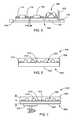
- the multi-chip package system 1400includes a package board 1402 , a first chip package 1404 , a second chip package 1406 , and a third chip package 1408 .
- the first chip package 1404 , the second chip package 1406 , and the third chip package 1408are encapsulated within an encapsulant 1410 , such as a molding compound.
- the package board 1402includes a substrate 1412 sandwiched between a first wiring layer 1414 and a second wiring layer 1416 . Vias 1418 electrically connect the first wiring layer 1414 and the second wiring layer 1416 .
- Solder balls 1420are mounted to the first wiring layer 1414 electrically connecting some of the vias 1418 .
- the first and second chip packages 1404 and 1406are similar to the chip package 1200 of FIG. 12 .
- the third chip package 1408is similar to the chip package 1300 of FIG. 13 .
- a first die 1405 of the first chip package 1404 and a second die 1407 of the second chip package 1406are die attached to the package board 1402 by an adhesive 1422 .
- a first interconnect 1424 of the first chip package 1404includes a first wire bond 1425 that is electrically connected to the second wiring layer 1416 by a first electrical connector or bond wire 1426 .
- a first interconnect 1428 of the second chip package 1406includes a second wire bond 1429 that is electrically connected to the second wiring layer 1416 by a second electrical connector or bond wire 1430 .
- a second interconnect 1432 of the first chip package 1404is in contact with a first small interconnect 1434 of a die 1435 of the third chip package 1408 .
- a second interconnect 1436 of the second chip package 1406is in contact with a second small interconnect 1438 of the third chip package 1408 .
- Large interconnects 1440 of the die 1435are in contact with the second wiring layer 1416 .
- the multi-chip package system 1400may be of a MCM type or MCM-SiP (with attached passive components).
- the multi-chip package system 1400may be of a laminate package.
- the third chip package 1408can include a live device or a dummy die.
- the live devicecan be either a chip or an integrated passive device (IPD).
- the dummy diemay consist of a silicon die with RDL layers to provide electrical connection between the small interconnects and large interconnects.
- the multi-chip package system 1500includes a package board 1502 , a first chip package 1504 , a second chip package 1506 , and a third chip package 1508 .
- the first chip package 1504 , the second chip package 1506 , and the third chip package 1508are partially encapsulated within an encapsulant 1510 , such as a molding compound.
- the package board 1502includes a substrate 1512 sandwiched between a first wiring layer 1514 and a second wiring layer 1516 . Vias 1518 electrically connect the first wiring layer 1514 and the second wiring layer 1516 .
- Solder balls 1520are mounted to the first wiring layer 1514 electrically connecting some of the vias 1518 .
- the first and second chip packages 1504 and 1506are similar to the second chip package 1300 of FIG. 13 .
- the third chip package 1508is similar to the first chip package 1200 of FIG. 12 .
- a first and a second die 1505 and 1507 of the first and second chip packages 1504 and 1506are die attached to the second wiring layer 1516 by adhesive 1522 .
- a first small interconnect 1524 of the first chip package 1504is electrically connected to the second wiring layer 1516 with a first electrically conductive wire 1526 .
- a first small interconnect 1528 of the second chip package 1506is electrically connected to the second wiring layer 1516 with a second electrically conductive wire 1530 .
- a second small interconnect 1532 of the first chip package 1504is in contact with a first interconnect 1534 of the third chip package 1508 .
- a second small interconnect 1536 of the second chip package 1506is in contact with a second interconnect 1538 of the third chip package 1508 .
- a top portion of large interconnects 1540 of the first chip package 1504 and the second chip package 1506are left exposed for stacking other die or chip packages.
- FIG. 16is a cross-sectional view of a multi-chip package system 1600 in accordance with a further embodiment of the present invention.
- the multi-chip package system 1600includes a chip 1602 mounted on the multi-chip package system 1500 .
- the chip 1602is electrically coupled to the top portion of the large interconnects 1540 with solder balls 1604 .
- the multi-chip package system 1700includes a chip package 1702 mounted on the multi-chip package system 1500 .
- the chip package 1702may include a BGA or a leaded type chip.
- the multi-chip package system 1800includes a package board 1802 , a first chip package 1804 .
- the first chip package 1804is partially encapsulated within a molding compound 1806 .
- the package board 1802includes a substrate 1808 sandwiched between a first circuit board 1810 and a second circuit board 1812 .
- Vias 1814electrically connect the first circuit board 1810 and the second circuit board 1812 .
- Solder balls 1816are mounted to the first circuit board 1810 electrically connecting some of the vias 1814 .
- the first chip package 1804is similar to the second wafer package 1300 of FIG. 13 .
- a semiconductor 1818 of the first chip package 1804is attached to the second circuit board 1812 with an adhesive 1820 .
- a first small interconnect 1822 of the first chip package 1804is electrically connected to the second circuit board 1812 with a first electrical connector 1824 .
- a second small interconnect 1826 of the first chip package 1804is electrically connected to the second circuit board 1812 with a second electrical connector 1828 .
- a top portion of large interconnects 1830 of the first chip package 1804is exposed and connected to a second chip package 1832 via solder balls 1834 .
- FIG. 19therein is shown a flow chart of a multi-chip package system 1900 for fabricating a first chip package in accordance with an embodiment of the present invention.
- the system 1900includes provided including providing a chip having interconnects provided thereon in a block 1902 ; forming a molding compound on the chip and encapsulating the interconnects in a block 1904 ; and forming a recess in the molding compound above the interconnects to expose the interconnects in a block 1906 .
- a method for fabricating the first chip packageis performed as follows:
- An aspectis that the present invention allows shorter die-to-die connection through various types of pre-encapsulated chip interconnects.
- Yet another aspect of the present inventionis that it valuably supports and services the historical trend of reducing costs, simplifying systems, and increasing performance.
Landscapes
- Engineering & Computer Science (AREA)
- Microelectronics & Electronic Packaging (AREA)
- Power Engineering (AREA)
- Computer Hardware Design (AREA)
- Physics & Mathematics (AREA)
- Condensed Matter Physics & Semiconductors (AREA)
- General Physics & Mathematics (AREA)
- Manufacturing & Machinery (AREA)
- Structures Or Materials For Encapsulating Or Coating Semiconductor Devices Or Solid State Devices (AREA)
Abstract
Description
- 1. providing a wafer mold. (
FIG. 6 ) - 2. grinding a bottom surface of the wafer mold. (
FIG. 7 ) - 3. grinding a top surface of the wafer mold to exposed large interconnects. (
FIG. 8 ) - 4. mounting the wafer mold on a dicing tape. (
FIG. 9 ) - 5. cutting through a portion of the wafer mold with thick blades to expose the small interconnects. (
FIG. 10 ) - 6. cutting through the wafer mold with thin blades to separate into individual single die. (
FIG. 11 )
- 1. providing a wafer mold. (
Claims (20)
Priority Applications (1)
| Application Number | Priority Date | Filing Date | Title |
|---|---|---|---|
| US11/326,211US7768125B2 (en) | 2006-01-04 | 2006-01-04 | Multi-chip package system |
Applications Claiming Priority (1)
| Application Number | Priority Date | Filing Date | Title |
|---|---|---|---|
| US11/326,211US7768125B2 (en) | 2006-01-04 | 2006-01-04 | Multi-chip package system |
Publications (2)
| Publication Number | Publication Date |
|---|---|
| US20070158809A1 US20070158809A1 (en) | 2007-07-12 |
| US7768125B2true US7768125B2 (en) | 2010-08-03 |
Family
ID=38232025
Family Applications (1)
| Application Number | Title | Priority Date | Filing Date |
|---|---|---|---|
| US11/326,211Active2027-02-23US7768125B2 (en) | 2006-01-04 | 2006-01-04 | Multi-chip package system |
Country Status (1)
| Country | Link |
|---|---|
| US (1) | US7768125B2 (en) |
Cited By (16)
| Publication number | Priority date | Publication date | Assignee | Title |
|---|---|---|---|---|
| US20060138649A1 (en)* | 2002-10-08 | 2006-06-29 | Chippac, Inc. | Semiconductor multi-package module having inverted second package stacked over die-up flip-chip ball grid array (BGA) package |
| US20080157331A1 (en)* | 2006-12-27 | 2008-07-03 | Masanori Onodera | Semiconductor device and method of manufacturing the same |
| US20100038781A1 (en)* | 2008-08-14 | 2010-02-18 | Dongsam Park | Integrated circuit packaging system having a cavity |
| US20100213593A1 (en)* | 2009-02-23 | 2010-08-26 | Samsung Electronics Co., Ltd. | Stacked semiconductor package |
| US20100301472A1 (en)* | 2009-06-02 | 2010-12-02 | Kabushiki Kaisha Toshiba | Electronic component and manufacturing method thereof |
| US8021924B2 (en) | 2005-03-31 | 2011-09-20 | Stats Chippac Ltd. | Encapsulant cavity integrated circuit package system and method of fabrication thereof |
| US20120231582A1 (en)* | 2008-11-26 | 2012-09-13 | Infineon Technologies Ag | Device including a semiconductor chip |
| US20130280861A1 (en)* | 2012-04-24 | 2013-10-24 | Micron Technology, Inc. | Methods for forming semiconductor device packages |
| JP2014024136A (en)* | 2012-07-25 | 2014-02-06 | Disco Abrasive Syst Ltd | Method of processing package substrate |
| US20140151700A1 (en)* | 2012-12-04 | 2014-06-05 | Thorsten Meyer | Chip package and a method for manufacturing a chip package |
| US20150061126A1 (en)* | 2013-08-30 | 2015-03-05 | Taiwan Semiconductor Manufacturing Company, Ltd. | Manufacture including substrate and package structure of optical chip |
| TWI578697B (en)* | 2015-12-07 | 2017-04-11 | 穩懋半導體股份有限公司 | Protection structure for semiconductor device package |
| US9883593B2 (en) | 2014-08-05 | 2018-01-30 | Samsung Electronics Co., Ltd. | Semiconductor modules and semiconductor packages |
| US20180270958A1 (en)* | 2017-03-17 | 2018-09-20 | Ibiden Co. , Ltd. | Printed wiring board and method for manufacturing the same |
| US10204814B1 (en)* | 2017-07-28 | 2019-02-12 | Stmicroelectronics, Inc. | Semiconductor package with individually molded leadframe and die coupled at solder balls |
| US11355470B2 (en)* | 2020-02-27 | 2022-06-07 | Amkor Technology Singapore Holding Pte. Ltd. | Semiconductor device and methods of manufacturing semiconductor devices |
Families Citing this family (14)
| Publication number | Priority date | Publication date | Assignee | Title |
|---|---|---|---|---|
| US7723146B2 (en)* | 2006-01-04 | 2010-05-25 | Stats Chippac Ltd. | Integrated circuit package system with image sensor system |
| US8704349B2 (en) | 2006-02-14 | 2014-04-22 | Stats Chippac Ltd. | Integrated circuit package system with exposed interconnects |
| US7385299B2 (en)* | 2006-02-25 | 2008-06-10 | Stats Chippac Ltd. | Stackable integrated circuit package system with multiple interconnect interface |
| US8581381B2 (en)* | 2006-06-20 | 2013-11-12 | Broadcom Corporation | Integrated circuit (IC) package stacking and IC packages formed by same |
| KR100771874B1 (en)* | 2006-07-06 | 2007-11-01 | 삼성전자주식회사 | Semiconductor tab package and manufacturing method thereof |
| JP2008130701A (en)* | 2006-11-20 | 2008-06-05 | Matsushita Electric Ind Co Ltd | WIRING BOARD, SEMICONDUCTOR DEVICE USING SAME, AND METHOD FOR MANUFACTURING SEMICONDUCTOR DEVICE |
| JP2008211125A (en) | 2007-02-28 | 2008-09-11 | Spansion Llc | Semiconductor device and its manufacturing method |
| US7859099B2 (en)* | 2008-12-11 | 2010-12-28 | Stats Chippac Ltd. | Integrated circuit packaging system having through silicon via with direct interconnects and method of manufacture thereof |
| US8110440B2 (en) | 2009-05-18 | 2012-02-07 | Stats Chippac, Ltd. | Semiconductor device and method of forming overlapping semiconductor die with coplanar vertical interconnect structure |
| JP2012204588A (en)* | 2011-03-25 | 2012-10-22 | Disco Abrasive Syst Ltd | Semiconductor device chip mounting method |
| KR101478601B1 (en)* | 2011-06-28 | 2015-01-05 | 하나 마이크론(주) | Semiconductor package and method of manufacturing the same |
| KR20130022821A (en)* | 2011-08-26 | 2013-03-07 | 삼성전자주식회사 | Stacked package and method of manufacturing the same |
| US8524577B2 (en)* | 2011-10-06 | 2013-09-03 | Stats Chippac, Ltd. | Semiconductor device and method of forming reconstituted wafer with larger carrier to achieve more eWLB packages per wafer with encapsulant deposited under temperature and pressure |
| JP2014007228A (en)* | 2012-06-22 | 2014-01-16 | Ps4 Luxco S A R L | Semiconductor device and manufacturing method of the same |
Citations (225)
| Publication number | Priority date | Publication date | Assignee | Title |
|---|---|---|---|---|
| US4524121A (en) | 1983-11-21 | 1985-06-18 | Rohm And Haas Company | Positive photoresists containing preformed polyglutarimide polymer |
| US4697203A (en) | 1984-06-04 | 1987-09-29 | Mitsubishi Denki Kabushiki Kaisha | Semiconductor device and manufacturing method therefor |
| US4764804A (en)* | 1986-02-21 | 1988-08-16 | Hitachi, Ltd. | Semiconductor device and process for producing the same |
| US4894707A (en) | 1987-02-12 | 1990-01-16 | Mitsubishi Denki Kabushiki Kaisha | Semiconductor device having a light transparent window and a method of producing same |
| EP0430458A2 (en) | 1989-12-01 | 1991-06-05 | STMicroelectronics Limited | Semiconductor chip packages |
| US5186383A (en)* | 1991-10-02 | 1993-02-16 | Motorola, Inc. | Method for forming solder bump interconnections to a solder-plated circuit trace |
| US5214308A (en)* | 1990-01-23 | 1993-05-25 | Sumitomo Electric Industries, Ltd. | Substrate for packaging a semiconductor device |
| US5214307A (en) | 1991-07-08 | 1993-05-25 | Micron Technology, Inc. | Lead frame for semiconductor devices having improved adhesive bond line control |
| US5222014A (en) | 1992-03-02 | 1993-06-22 | Motorola, Inc. | Three-dimensional multi-chip pad array carrier |
| US5229960A (en) | 1990-12-05 | 1993-07-20 | Matra Marconi Space France | Solid state memory modules and memory devices including such modules |
| US5269453A (en)* | 1992-04-02 | 1993-12-14 | Motorola, Inc. | Low temperature method for forming solder bump interconnections to a plated circuit trace |
| US5340771A (en) | 1993-03-18 | 1994-08-23 | Lsi Logic Corporation | Techniques for providing high I/O count connections to semiconductor dies |
| US5373189A (en) | 1992-08-13 | 1994-12-13 | Commissariate A L'energie Atomique | Three-dimensional multichip module |
| EP0652630A2 (en) | 1993-11-05 | 1995-05-10 | Kabushiki Kaisha Toshiba | Semiconductor stack |
| US5436203A (en) | 1994-07-05 | 1995-07-25 | Motorola, Inc. | Shielded liquid encapsulated semiconductor device and method for making the same |
| US5444296A (en) | 1993-11-22 | 1995-08-22 | Sun Microsystems, Inc. | Ball grid array packages for high speed applications |
| US5495398A (en) | 1992-05-22 | 1996-02-27 | National Semiconductor Corporation | Stacked multi-chip modules and method of manufacturing |
| US5550711A (en) | 1990-08-01 | 1996-08-27 | Staktek Corporation | Ultra high density integrated circuit packages |
| US5579207A (en) | 1994-10-20 | 1996-11-26 | Hughes Electronics | Three-dimensional integrated circuit stacking |
| US5607227A (en) | 1993-08-27 | 1997-03-04 | Sanyo Electric Co., Ltd. | Linear light source |
| US5650667A (en) | 1995-10-30 | 1997-07-22 | National Semiconductor Corporation | Process of forming conductive bumps on the electrodes of semiconductor chips using lapping and the bumps thereby created |
| US5652185A (en) | 1995-04-07 | 1997-07-29 | National Semiconductor Corporation | Maximized substrate design for grid array based assemblies |
| US5734199A (en)* | 1995-12-18 | 1998-03-31 | Matsushita Electric Industrial Co., Ltd. | Semiconductor device having improved test electrodes |
| US5744863A (en) | 1994-07-11 | 1998-04-28 | International Business Machines Corporation | Chip carrier modules with heat sinks attached by flexible-epoxy |
| US5748452A (en) | 1996-07-23 | 1998-05-05 | International Business Machines Corporation | Multi-electronic device package |
| US5760478A (en)* | 1996-08-20 | 1998-06-02 | International Business Machines Corporation | Clock skew minimization system and method for integrated circuits |
| US5824569A (en)* | 1992-07-15 | 1998-10-20 | Micron Technology, Inc. | Semiconductor device having ball-bonded pads |
| US5828128A (en)* | 1995-08-01 | 1998-10-27 | Fujitsu, Ltd. | Semiconductor device having a bump which is inspected from outside and a circuit board used with such a semiconductor device |
| US5844315A (en) | 1996-03-26 | 1998-12-01 | Motorola Corporation | Low-profile microelectronic package |
| US5854507A (en) | 1998-07-21 | 1998-12-29 | Hewlett-Packard Company | Multiple chip assembly |
| US5898219A (en) | 1997-04-02 | 1999-04-27 | Intel Corporation | Custom corner attach heat sink design for a plastic ball grid array integrated circuit package |
| US5899705A (en) | 1997-11-20 | 1999-05-04 | Akram; Salman | Stacked leads-over chip multi-chip module |
| US5903049A (en) | 1997-10-29 | 1999-05-11 | Mitsubishi Denki Kabushiki Kaisha | Semiconductor module comprising semiconductor packages |
| US5977641A (en)* | 1997-05-14 | 1999-11-02 | Kabushiki Kaisha Toshiba | Semiconductor device and method for manufacturing the same |
| US5977640A (en)* | 1998-06-26 | 1999-11-02 | International Business Machines Corporation | Highly integrated chip-on-chip packaging |
| US5982633A (en) | 1997-08-20 | 1999-11-09 | Compaq Computer Corporation | Opposed ball grid array mounting |
| US5994166A (en) | 1997-03-10 | 1999-11-30 | Micron Technology, Inc. | Method of constructing stacked packages |
| US6025648A (en) | 1997-04-17 | 2000-02-15 | Nec Corporation | Shock resistant semiconductor device and method for producing same |
| US6034875A (en) | 1998-06-17 | 2000-03-07 | International Business Machines Corporation | Cooling structure for electronic components |
| USRE36613E (en) | 1993-04-06 | 2000-03-14 | Micron Technology, Inc. | Multi-chip stacked devices |
| US6075289A (en) | 1996-10-24 | 2000-06-13 | Tessera, Inc. | Thermally enhanced packaged semiconductor assemblies |
| US6083811A (en) | 1996-02-07 | 2000-07-04 | Northrop Grumman Corporation | Method for producing thin dice from fragile materials |
| US6083775A (en) | 1998-02-07 | 2000-07-04 | Siliconware Precision Industries Co., Ltd. | Method of encapsulating a chip |
| US6107164A (en)* | 1998-08-18 | 2000-08-22 | Oki Electric Industry Co., Ltd. | Using grooves as alignment marks when dicing an encapsulated semiconductor wafer |
| US6118176A (en) | 1999-04-26 | 2000-09-12 | Advanced Semiconductor Engineering, Inc. | Stacked chip assembly utilizing a lead frame |
| US6121682A (en)* | 1998-12-26 | 2000-09-19 | Hyundai Electronics Industries Co., Ltd. | Multi-chip package |
| US6130448A (en) | 1998-08-21 | 2000-10-10 | Gentex Corporation | Optical sensor package and method of making same |
| US6144507A (en) | 1996-07-23 | 2000-11-07 | Seiko Epson Corporation | Method of mounting a sealed assembly on a mounting substrate and optical transducer |
| US6143588A (en) | 1997-09-09 | 2000-11-07 | Amkor Technology, Inc. | Method of making an integrated circuit package employing a transparent encapsulant |
| US6157080A (en) | 1997-11-06 | 2000-12-05 | Sharp Kabushiki Kaisha | Semiconductor device using a chip scale package |
| US6165815A (en) | 1996-02-20 | 2000-12-26 | Micron Technology, Inc. | Method of fabrication of stacked semiconductor devices |
| US6201302B1 (en) | 1998-12-31 | 2001-03-13 | Sampo Semiconductor Corporation | Semiconductor package having multi-dies |
| US6201266B1 (en) | 1999-07-01 | 2001-03-13 | Oki Electric Industry Co., Ltd. | Semiconductor device and method for manufacturing the same |
| US6204562B1 (en) | 1999-02-11 | 2001-03-20 | United Microelectronics Corp. | Wafer-level chip scale package |
| US6225699B1 (en)* | 1998-06-26 | 2001-05-01 | International Business Machines Corporation | Chip-on-chip interconnections of varied characteristics |
| US6238949B1 (en) | 1999-06-18 | 2001-05-29 | National Semiconductor Corporation | Method and apparatus for forming a plastic chip on chip package module |
| US6242932B1 (en) | 1999-02-19 | 2001-06-05 | Micron Technology, Inc. | Interposer for semiconductor components having contact balls |
| US6246123B1 (en) | 1998-05-04 | 2001-06-12 | Motorola, Inc. | Transparent compound and applications for its use |
| US6265766B1 (en) | 1995-12-19 | 2001-07-24 | Micron Technology, Inc. | Flip chip adaptor package for bare die |
| US6266197B1 (en) | 1999-12-08 | 2001-07-24 | Amkor Technology, Inc. | Molded window array for image sensor packages |
| US6274930B1 (en) | 1999-08-17 | 2001-08-14 | Micron Technology, Inc. | Multi-chip module with stacked dice |
| JP2001223326A (en) | 2000-02-09 | 2001-08-17 | Hitachi Ltd | Semiconductor device |
| US6291263B1 (en) | 2000-06-13 | 2001-09-18 | Siliconware Precision Industries Co., Ltd. | Method of fabricating an integrated circuit package having a core-hollowed encapsulation body |
| US6297131B1 (en) | 1999-04-22 | 2001-10-02 | Fujitsu Limited | Semiconductor device manufacturing method for grinding and dicing a wafer from a back side of the wafer |
| US6316735B1 (en)* | 1996-11-08 | 2001-11-13 | Ricoh Company, Ltd. | Semiconductor chip mounting board and a semiconductor device using same board |
| US6316838B1 (en) | 1999-10-29 | 2001-11-13 | Fujitsu Limited | Semiconductor device |
| US6333552B1 (en) | 1998-08-07 | 2001-12-25 | Sharp Kabushiki Kaisha | Millimeter wave semiconductor device |
| US20010055834A1 (en) | 2000-06-21 | 2001-12-27 | Advanced Semiconductor Engineering, Inc. | Method of making semiconductor packages at wafer level |
| US6340846B1 (en) | 2000-12-06 | 2002-01-22 | Amkor Technology, Inc. | Making semiconductor packages with stacked dies and reinforced wire bonds |
| US20020024124A1 (en)* | 1997-03-10 | 2002-02-28 | Nobuaki Hashimoto | Electronic component and semiconductor device, method for manufacturing the same, circuit board have the same mounted thereon, and electronic equipment having the circuit board |
| US6353257B1 (en) | 2000-05-19 | 2002-03-05 | Siliconware Precision Industries Co., Ltd. | Semiconductor package configuration based on lead frame having recessed and shouldered portions for flash prevention |
| US6358773B1 (en) | 2000-12-27 | 2002-03-19 | Vincent Lin | Method of making substrate for use in forming image sensor package |
| US6369454B1 (en) | 1998-12-31 | 2002-04-09 | Amkor Technology, Inc. | Semiconductor package and method for fabricating the same |
| US6372551B1 (en) | 2000-05-12 | 2002-04-16 | Siliconware Precison Industries Co., Ltd. | Method of manufacturing an image-sensor integrated circuit package without resin flash on lead frame and with increased wire bondability |
| US6376904B1 (en) | 1999-12-23 | 2002-04-23 | Rambus Inc. | Redistributed bond pads in stacked integrated circuit die package |
| US6379988B1 (en) | 2000-05-16 | 2002-04-30 | Sandia Corporation | Pre-release plastic packaging of MEMS and IMEMS devices |
| US6384472B1 (en) | 2000-03-24 | 2002-05-07 | Siliconware Precision Industries Co., Ltd | Leadless image sensor package structure and method for making the same |
| US6388313B1 (en) | 2001-01-30 | 2002-05-14 | Siliconware Precision Industries Co., Ltd. | Multi-chip module |
| US6400007B1 (en) | 2001-04-16 | 2002-06-04 | Kingpak Technology Inc. | Stacked structure of semiconductor means and method for manufacturing the same |
| US6407456B1 (en) | 1996-02-20 | 2002-06-18 | Micron Technology, Inc. | Multi-chip device utilizing a flip chip and wire bond assembly |
| US6407381B1 (en) | 2000-07-05 | 2002-06-18 | Amkor Technology, Inc. | Wafer scale image sensor package |
| US6410861B1 (en)* | 1999-12-03 | 2002-06-25 | Motorola, Inc. | Low profile interconnect structure |
| US6413798B2 (en) | 1998-01-18 | 2002-07-02 | Kabushiki Kaisha Toshiba | Package having very thin semiconductor chip, multichip module assembled by the package, and method for manufacturing the same |
| US6414381B1 (en) | 1999-03-15 | 2002-07-02 | Fujitsu Media Devices Limited | Interposer for separating stacked semiconductor chips mounted on a multi-layer printed circuit board |
| US6420204B2 (en) | 1999-06-03 | 2002-07-16 | Amkor Technology, Inc. | Method of making a plastic package for an optical integrated circuit device |
| US6420244B2 (en) | 2000-02-21 | 2002-07-16 | Advanced Semiconductor Engineering, Inc. | Method of making wafer level chip scale package |
| US6424050B1 (en) | 1999-09-22 | 2002-07-23 | Seiko Epson Corporation | Semiconductor device |
| US20020096755A1 (en) | 2001-01-24 | 2002-07-25 | Yasuki Fukui | Semiconductor device |
| US20020100955A1 (en)* | 1999-02-22 | 2002-08-01 | Scott G. Potter | Method and apparatus for extending fatigue life of solder joints semiconductor device |
| US6441496B1 (en) | 2000-11-22 | 2002-08-27 | Wen Chuan Chen | Structure of stacked integrated circuits |
| US6445064B1 (en) | 2001-02-06 | 2002-09-03 | Mitsubishi Denki Kabushiki Kaisha | Semiconductor device |
| US20020130404A1 (en) | 2001-03-19 | 2002-09-19 | Toshihiro Ushijima | Semiconductor module in which plural semiconductor chips are enclosed in one package |
| US6462421B1 (en) | 2000-04-10 | 2002-10-08 | Advanced Semicondcutor Engineering, Inc. | Multichip module |
| US6472732B1 (en) | 1999-10-25 | 2002-10-29 | Oki Electric Industry Co., Ltd. | BGA package and method for fabricating the same |
| US6489676B2 (en) | 2000-12-04 | 2002-12-03 | Fujitsu Limited | Semiconductor device having an interconnecting post formed on an interposer within a sealing resin |
| US6492726B1 (en) | 2000-09-22 | 2002-12-10 | Chartered Semiconductor Manufacturing Ltd. | Chip scale packaging with multi-layer flip chip arrangement and ball grid array interconnection |
| US6501165B1 (en) | 1998-06-05 | 2002-12-31 | Micron Technology, Inc. | Stackable semiconductor package having conductive layer and insulating layers and method of fabrication |
| US6503780B1 (en) | 2000-07-05 | 2003-01-07 | Amkor Technology, Inc. | Wafer scale image sensor package fabrication method |
| US20030008510A1 (en) | 2000-12-06 | 2003-01-09 | Grigg Ford B. | Thin flip-chip method |
| US6509639B1 (en) | 2001-07-27 | 2003-01-21 | Charles W. C. Lin | Three-dimensional stacked semiconductor package |
| US6512219B1 (en) | 2000-01-25 | 2003-01-28 | Amkor Technology, Inc. | Fabrication method for integrally connected image sensor packages having a window support in contact with the window and active area |
| US20030038347A1 (en) | 2001-08-22 | 2003-02-27 | Walton Advanced Electronics Ltd | Stackable-type semiconductor package |
| US6529027B1 (en) | 2000-03-23 | 2003-03-04 | Micron Technology, Inc. | Interposer and methods for fabricating same |
| US6534419B1 (en) | 2000-07-26 | 2003-03-18 | Advanced Interconnect Solutions | Method and apparatus for reducing IC die mass and thickness while improving strength characteristics |
| US6538319B2 (en) | 1997-09-02 | 2003-03-25 | Oki Electric Industry Co., Ltd. | Semiconductor device |
| US6541857B2 (en)* | 1999-10-25 | 2003-04-01 | International Business Machines Corporation | Method of forming BGA interconnections having mixed solder profiles |
| US6545365B2 (en) | 2000-04-26 | 2003-04-08 | Mitsubishi Denki Kabushiki Kaisha | Resin-sealed chip stack type semiconductor device |
| US6545366B2 (en) | 2001-01-11 | 2003-04-08 | Mitsubishi Denki Kabushiki Kaisha | Multiple chip package semiconductor device |
| US6552423B2 (en) | 2000-02-18 | 2003-04-22 | Samsung Electronics Co., Ltd. | Higher-density memory card |
| US6555902B2 (en) | 2000-07-17 | 2003-04-29 | Siliconware Precision Industries Co., Ltd. | Multiple stacked-chip packaging structure |
| US6555917B1 (en) | 2001-10-09 | 2003-04-29 | Amkor Technology, Inc. | Semiconductor package having stacked semiconductor chips and method of making the same |
| US6566745B1 (en) | 1999-03-29 | 2003-05-20 | Imec Vzw | Image sensor ball grid array package and the fabrication thereof |
| US6570249B1 (en) | 2001-12-24 | 2003-05-27 | Siliconware Precision Industries Co., Ltd. | Semiconductor package |
| US6580169B2 (en)* | 1999-12-27 | 2003-06-17 | Fujitsu Limited | Method for forming bumps, semiconductor device, and solder paste |
| US20030113952A1 (en) | 2001-12-19 | 2003-06-19 | Mahesh Sambasivam | Underfill materials dispensed in a flip chip package by way of a through hole |
| US6590281B2 (en) | 2001-11-15 | 2003-07-08 | Siliconware Precision Industries Co., Ltd. | Crack-preventive semiconductor package |
| US6593648B2 (en) | 2000-08-31 | 2003-07-15 | Seiko Epson Corporation | Semiconductor device and method of making the same, circuit board and electronic equipment |
| US6593647B2 (en) | 2001-06-15 | 2003-07-15 | Oki Electric Industry Co., Ltd. | Semiconductor device |
| US6593662B1 (en) | 2000-06-16 | 2003-07-15 | Siliconware Precision Industries Co., Ltd. | Stacked-die package structure |
| US6599779B2 (en) | 2001-09-24 | 2003-07-29 | St Assembly Test Service Ltd. | PBGA substrate for anchoring heat sink |
| US20030153134A1 (en) | 1998-06-01 | 2003-08-14 | Youichi Kawata | Semiconductor device, and a method of producing semiconductor device |
| US6607937B1 (en) | 2000-08-23 | 2003-08-19 | Micron Technology, Inc. | Stacked microelectronic dies and methods for stacking microelectronic dies |
| US6611063B1 (en) | 1999-09-16 | 2003-08-26 | Nec Electronics Corporation | Resin-encapsulated semiconductor device |
| US6610563B1 (en) | 1997-12-15 | 2003-08-26 | Osram Opto Semiconductors Gmbh & Co. Ohg | Surface mounting optoelectronic component and method for producing same |
| US6613980B1 (en) | 2002-03-11 | 2003-09-02 | Agilent Technologies, Inc. | Environmental protection for an optical assembly and method therefor |
| US6617198B2 (en) | 2001-01-17 | 2003-09-09 | Micron Technology, Inc. | Semiconductor assembly without adhesive fillets |
| US6621172B2 (en) | 1999-09-03 | 2003-09-16 | Seiko Epson Corporation | Semiconductor device and method of fabricating the same, circuit board, and electronic equipment |
| US6621169B2 (en) | 2000-09-04 | 2003-09-16 | Fujitsu Limited | Stacked semiconductor device and method of producing the same |
| US6627864B1 (en) | 1999-11-22 | 2003-09-30 | Amkor Technology, Inc. | Thin image sensor package |
| US6627979B2 (en)* | 2001-06-15 | 2003-09-30 | Dongbu Electronics Co., Ltd. | Semiconductor package and fabrication method of the same |
| US6642609B1 (en) | 1999-09-01 | 2003-11-04 | Matsushita Electric Industrial Co., Ltd. | Leadframe for a semiconductor device having leads with land electrodes |
| US6649448B2 (en) | 2000-10-05 | 2003-11-18 | Hitachi, Ltd. | Method of manufacturing a semiconductor device having flexible wiring substrate |
| US6649445B1 (en)* | 2002-09-11 | 2003-11-18 | Motorola, Inc. | Wafer coating and singulation method |
| US6650019B2 (en) | 2000-07-20 | 2003-11-18 | Amkor Technology, Inc. | Method of making a semiconductor package including stacked semiconductor dies |
| US6674156B1 (en) | 2001-02-09 | 2004-01-06 | National Semiconductor Corporation | Multiple row fine pitch leadless leadframe package with use of half-etch process |
| US20040016939A1 (en) | 2002-07-26 | 2004-01-29 | Masayuki Akiba | Encapsulation of a stack of semiconductor dice |
| US6690089B2 (en) | 2002-05-15 | 2004-02-10 | Oki Electric Industry Co., Ltd. | Semiconductor device having multi-chip package |
| US6693364B2 (en) | 2002-06-20 | 2004-02-17 | Advanced Semiconductor Engineering, Inc. | Optical integrated circuit element package and process for making the same |
| US6692993B2 (en) | 1998-10-13 | 2004-02-17 | Intel Corporation | Windowed non-ceramic package having embedded frame |
| US6700178B2 (en) | 2001-03-09 | 2004-03-02 | Advanced Semiconductor Engineering, Inc. | Package of a chip with beveled edges |
| US6700192B2 (en) | 2001-10-16 | 2004-03-02 | Shinko Electric Industries Co., Ltd. | Leadframe and method of manufacturing a semiconductor device using the same |
| US6707140B1 (en) | 2000-05-09 | 2004-03-16 | National Semiconductor Corporation | Arrayable, scaleable, and stackable molded package configuration |
| US6706557B2 (en) | 2001-09-21 | 2004-03-16 | Micron Technology, Inc. | Method of fabricating stacked die configurations utilizing redistribution bond pads |
| US6713366B2 (en) | 2002-06-12 | 2004-03-30 | Intel Corporation | Method of thinning a wafer utilizing a laminated reinforcing layer over the device side |
| US20040061213A1 (en) | 2002-09-17 | 2004-04-01 | Chippac, Inc. | Semiconductor multi-package module having package stacked over die-up flip chip ball grid array package and having wire bond interconnect between stacked packages |
| US6716670B1 (en) | 2002-01-09 | 2004-04-06 | Bridge Semiconductor Corporation | Method of forming a three-dimensional stacked semiconductor package device |
| US6734569B2 (en) | 1998-07-13 | 2004-05-11 | International Business Machines Corporation | Die attachment with reduced adhesive bleed-out |
| US6734552B2 (en) | 2001-07-11 | 2004-05-11 | Asat Limited | Enhanced thermal dissipation integrated circuit package |
| US6734539B2 (en) | 2000-12-27 | 2004-05-11 | Lucent Technologies Inc. | Stacked module package |
| US6737750B1 (en) | 2001-12-07 | 2004-05-18 | Amkor Technology, Inc. | Structures for improving heat dissipation in stacked semiconductor packages |
| US6740980B2 (en)* | 2002-07-04 | 2004-05-25 | Renesas Technology Corp. | Semiconductor device |
| US6747361B2 (en) | 2000-07-26 | 2004-06-08 | Nec Electronics Corporation | Semiconductor device and packaging method thereof |
| US6746894B2 (en) | 2001-03-30 | 2004-06-08 | Micron Technology, Inc. | Ball grid array interposer, packages and methods |
| US20040119153A1 (en) | 2002-10-08 | 2004-06-24 | Chippac, Inc. | Semiconductor multi-package module having inverted land grid array (LGA) package stacked over ball grid array (BGA) package |
| US20040124540A1 (en)* | 2002-12-30 | 2004-07-01 | Yu-Wen Chen | [flip chip package structure] |
| US6762488B2 (en) | 2002-03-19 | 2004-07-13 | Nec Electronics Corporation | Light thin stacked package semiconductor device and process for fabrication thereof |
| US6774475B2 (en) | 2002-01-24 | 2004-08-10 | International Business Machines Corporation | Vertically stacked memory chips in FBGA packages |
| US6777819B2 (en) | 2000-12-20 | 2004-08-17 | Siliconware Precision Industries Co., Ltd. | Semiconductor package with flash-proof device |
| US20040166605A1 (en) | 2002-10-10 | 2004-08-26 | Bunshi Kuratomi | Fabrication method of semiconductor integrated circuit device |
| US6784534B1 (en) | 2002-02-06 | 2004-08-31 | Amkor Technology, Inc. | Thin integrated circuit package having an optically transparent window |
| US6787915B2 (en) | 2001-03-05 | 2004-09-07 | Oki Electric Industry Co., Ltd. | Rearrangement sheet, semiconductor device and method of manufacturing thereof |
| US6787916B2 (en) | 2001-09-13 | 2004-09-07 | Tru-Si Technologies, Inc. | Structures having a substrate with a cavity and having an integrated circuit bonded to a contact pad located in the cavity |
| US6791036B1 (en) | 1997-12-08 | 2004-09-14 | 3M Innovative Properties Company | Circuit elements using z-axis interconnect |
| US6791168B1 (en) | 2002-07-10 | 2004-09-14 | Micron Technology, Inc. | Semiconductor package with circuit side polymer layer and wafer level fabrication method |
| US6791076B2 (en) | 1999-12-08 | 2004-09-14 | Amkor Technology, Inc. | Image sensor package |
| US6794749B2 (en) | 1999-08-31 | 2004-09-21 | Micron Technology, Inc. | Chip package with grease heat sink |
| US20040201087A1 (en) | 2003-01-03 | 2004-10-14 | Dong-Ho Lee | Stack package made of chip scale packages |
| US6809405B2 (en) | 2001-12-14 | 2004-10-26 | Renesas Technology Corp. | Semiconductor device and method of manufacturing the same |
| US20040212096A1 (en) | 2003-04-23 | 2004-10-28 | Advanced Semiconductor Engineering, Inc. | Multi-chips stacked package |
| US6815254B2 (en) | 2003-03-10 | 2004-11-09 | Freescale Semiconductor, Inc. | Semiconductor package with multiple sides having package contacts |
| US6818980B1 (en) | 2003-05-07 | 2004-11-16 | Asat Ltd. | Stacked semiconductor package and method of manufacturing the same |
| US6828665B2 (en) | 2002-10-18 | 2004-12-07 | Siliconware Precision Industries Co., Ltd. | Module device of stacked semiconductor packages and method for fabricating the same |
| US6833612B2 (en) | 2002-08-29 | 2004-12-21 | Micron Technology, Inc. | Flip-chip image sensor packages |
| US6835598B2 (en) | 2002-07-24 | 2004-12-28 | Samsung Electronics Co., Ltd. | Stacked semiconductor module and method of manufacturing the same |
| US6838761B2 (en) | 2002-09-17 | 2005-01-04 | Chippac, Inc. | Semiconductor multi-package module having wire bond interconnect between stacked packages and having electrical shield |
| US6847109B2 (en) | 2002-09-25 | 2005-01-25 | Samsung Electronics Co., Ltd. | Area array semiconductor package and 3-dimensional stack thereof |
| US6851598B2 (en)* | 2001-07-25 | 2005-02-08 | Infineon Technologies Ag | Electronic component with a semiconductor chip and method for producing the electronic component |
| US6852570B2 (en)* | 2002-07-12 | 2005-02-08 | Oki Electric Industry Co., Ltd. | Method of manufacturing a stacked semiconductor device |
| US6861683B2 (en) | 2001-04-11 | 2005-03-01 | Dr. Johannes Heidenhain Gmbh | Optoelectronic component using two encapsulating materials and the method of making the same |
| US6861288B2 (en) | 2003-01-23 | 2005-03-01 | St Assembly Test Services, Ltd. | Stacked semiconductor packages and method for the fabrication thereof |
| US6864566B2 (en) | 2001-08-21 | 2005-03-08 | Samsung Electronics Co., Ltd. | Duel die package |
| US20050051882A1 (en) | 2001-06-29 | 2005-03-10 | Kwon Yong Hwan | Stacked chip package having upper chip provided with trenches and method of manufacturing the same |
| US20050075053A1 (en) | 2003-10-02 | 2005-04-07 | Meng-An Jung | Back grinding methods for fabricating an image sensor |
| US6882057B2 (en) | 2003-06-25 | 2005-04-19 | Via Technologies, Inc. | Quad flat no-lead chip carrier |
| US6881611B1 (en)* | 1996-07-12 | 2005-04-19 | Fujitsu Limited | Method and mold for manufacturing semiconductor device, semiconductor device and method for mounting the device |
| US6890798B2 (en) | 1999-06-08 | 2005-05-10 | Intel Corporation | Stacked chip packaging |
| US6891239B2 (en) | 2002-03-06 | 2005-05-10 | The Charles Stark Draper Laboratory, Inc. | Integrated sensor and electronics package |
| US6900079B2 (en) | 2000-06-02 | 2005-05-31 | Micron Technology, Inc. | Method for fabricating a chip scale package using wafer level processing |
| US6900528B2 (en) | 2001-06-21 | 2005-05-31 | Micron Technology, Inc. | Stacked mass storage flash memory package |
| US6906415B2 (en) | 2002-06-27 | 2005-06-14 | Micron Technology, Inc. | Semiconductor device assemblies and packages including multiple semiconductor devices and methods |
| US6916683B2 (en) | 2000-05-11 | 2005-07-12 | Micron Technology, Inc. | Methods of fabricating a molded ball grid array |
| US6930378B1 (en) | 2003-11-10 | 2005-08-16 | Amkor Technology, Inc. | Stacked semiconductor die assembly having at least one support |
| US6930396B2 (en) | 2002-04-05 | 2005-08-16 | Nec Electronics Corporation | Semiconductor device and method for manufacturing the same |
| US6951982B2 (en) | 2002-11-22 | 2005-10-04 | Micron Technology, Inc. | Packaged microelectronic component assemblies |
| US6972481B2 (en) | 2002-09-17 | 2005-12-06 | Chippac, Inc. | Semiconductor multi-package module including stacked-die package and having wire bond interconnect between stacked packages |
| US20060043556A1 (en) | 2004-08-25 | 2006-03-02 | Chao-Yuan Su | Stacked packaging methods and structures |
| US20060065958A1 (en) | 2004-09-29 | 2006-03-30 | Pei-Haw Tsao | Three dimensional package and packaging method for integrated circuits |
| US20060073635A1 (en) | 2004-09-28 | 2006-04-06 | Chao-Yuan Su | Three dimensional package type stacking for thinner package application |
| US7034387B2 (en) | 2003-04-04 | 2006-04-25 | Chippac, Inc. | Semiconductor multipackage module including processor and memory package assemblies |
| US7034388B2 (en) | 2002-01-25 | 2006-04-25 | Advanced Semiconductor Engineering, Inc. | Stack type flip-chip package |
| US7053476B2 (en) | 2002-09-17 | 2006-05-30 | Chippac, Inc. | Semiconductor multi-package module having package stacked over die-down flip chip ball grid array package and having wire bond interconnect between stacked packages |
| US7064426B2 (en) | 2002-09-17 | 2006-06-20 | Chippac, Inc. | Semiconductor multi-package module having wire bond interconnect between stacked packages |
| US20060138631A1 (en) | 2003-12-31 | 2006-06-29 | Advanced Semiconductor Engineering, Inc. | Multi-chip package structure |
| US7081678B2 (en) | 2003-04-04 | 2006-07-25 | Advanced Semiconductor Engineering Inc. | Multi-chip package combining wire-bonding and flip-chip configuration |
| US7084500B2 (en)* | 2003-10-29 | 2006-08-01 | Texas Instruments Incorporated | Semiconductor circuit with multiple contact sizes |
| US7090482B2 (en)* | 1999-07-16 | 2006-08-15 | Matsushita Electric Industrial Co., Ltd. | Semiconductor device package manufacturing method and semiconductor device package manufactured by the method |
| US20060189033A1 (en) | 2005-02-04 | 2006-08-24 | Stats Chippac Ltd. | Integrated circuit package-in-package system |
| US20060197209A1 (en) | 2005-02-10 | 2006-09-07 | Stats Chippac Ltd. | Stacked integrated circuits package system with dense routability and high thermal conductivity |
| US7109574B2 (en) | 2002-07-26 | 2006-09-19 | Stmicroelectronics, Inc. | Integrated circuit package with exposed die surfaces and auxiliary attachment |
| US7115990B2 (en) | 2001-05-21 | 2006-10-03 | Micron Technology, Inc. | Bumped die and wire bonded board-on-chip package |
| US7119427B2 (en) | 2003-11-13 | 2006-10-10 | Samsung Electronics Ltd., Co. | Stacked BGA packages |
| US7122906B2 (en)* | 2004-01-29 | 2006-10-17 | Micron Technology, Inc. | Die-wafer package and method of fabricating same |
| US20060244157A1 (en) | 2005-04-29 | 2006-11-02 | Flynn Carson | Stacked integrated circuit package system |
| US7176506B2 (en) | 2001-08-28 | 2007-02-13 | Tessera, Inc. | High frequency chip packages with connecting elements |
| US7218005B2 (en)* | 2000-12-01 | 2007-05-15 | Nec Corporation | Compact semiconductor device capable of mounting a plurality of semiconductor chips with high density and method of manufacturing the same |
| US7221059B2 (en)* | 2002-03-06 | 2007-05-22 | Micron Technology, Inc. | Wafer level semiconductor component having thinned, encapsulated dice and polymer dam |
| US20070141751A1 (en) | 2005-12-16 | 2007-06-21 | Mistry Addi B | Stackable molded packages and methods of making the same |
| US20070148822A1 (en) | 2005-12-23 | 2007-06-28 | Tessera, Inc. | Microelectronic packages and methods therefor |
| US20070166867A1 (en) | 2006-01-04 | 2007-07-19 | Chow Seng G | Integrated circuit package system with image sensor system |
| US7298045B2 (en) | 2003-11-28 | 2007-11-20 | Matsushita Electric Industrial Co., Ltd | Stacked semiconductor device |
| US7335994B2 (en)* | 2003-01-27 | 2008-02-26 | Micron Technology, Inc. | Semiconductor component having multiple stacked dice |
| US7355274B2 (en) | 2004-12-10 | 2008-04-08 | Samsung Electronics Co., Ltd. | Semiconductor package, manufacturing method thereof and IC chip |
| US7364945B2 (en) | 2005-03-31 | 2008-04-29 | Stats Chippac Ltd. | Method of mounting an integrated circuit package in an encapsulant cavity |
| US7372141B2 (en) | 2005-03-31 | 2008-05-13 | Stats Chippac Ltd. | Semiconductor stacked package assembly having exposed substrate surfaces on upper and lower sides |
| US7456088B2 (en) | 2006-01-04 | 2008-11-25 | Stats Chippac Ltd. | Integrated circuit package system including stacked die |
- 2006
- 2006-01-04USUS11/326,211patent/US7768125B2/enactiveActive
Patent Citations (248)
| Publication number | Priority date | Publication date | Assignee | Title |
|---|---|---|---|---|
| US4524121A (en) | 1983-11-21 | 1985-06-18 | Rohm And Haas Company | Positive photoresists containing preformed polyglutarimide polymer |
| US4697203A (en) | 1984-06-04 | 1987-09-29 | Mitsubishi Denki Kabushiki Kaisha | Semiconductor device and manufacturing method therefor |
| US4764804A (en)* | 1986-02-21 | 1988-08-16 | Hitachi, Ltd. | Semiconductor device and process for producing the same |
| US4894707A (en) | 1987-02-12 | 1990-01-16 | Mitsubishi Denki Kabushiki Kaisha | Semiconductor device having a light transparent window and a method of producing same |
| EP0430458A2 (en) | 1989-12-01 | 1991-06-05 | STMicroelectronics Limited | Semiconductor chip packages |
| US5214308A (en)* | 1990-01-23 | 1993-05-25 | Sumitomo Electric Industries, Ltd. | Substrate for packaging a semiconductor device |
| US5550711A (en) | 1990-08-01 | 1996-08-27 | Staktek Corporation | Ultra high density integrated circuit packages |
| US5229960A (en) | 1990-12-05 | 1993-07-20 | Matra Marconi Space France | Solid state memory modules and memory devices including such modules |
| US5214307A (en) | 1991-07-08 | 1993-05-25 | Micron Technology, Inc. | Lead frame for semiconductor devices having improved adhesive bond line control |
| US5186383A (en)* | 1991-10-02 | 1993-02-16 | Motorola, Inc. | Method for forming solder bump interconnections to a solder-plated circuit trace |
| US5222014A (en) | 1992-03-02 | 1993-06-22 | Motorola, Inc. | Three-dimensional multi-chip pad array carrier |
| US5269453A (en)* | 1992-04-02 | 1993-12-14 | Motorola, Inc. | Low temperature method for forming solder bump interconnections to a plated circuit trace |
| US5495398A (en) | 1992-05-22 | 1996-02-27 | National Semiconductor Corporation | Stacked multi-chip modules and method of manufacturing |
| US5824569A (en)* | 1992-07-15 | 1998-10-20 | Micron Technology, Inc. | Semiconductor device having ball-bonded pads |
| US5373189A (en) | 1992-08-13 | 1994-12-13 | Commissariate A L'energie Atomique | Three-dimensional multichip module |
| US5340771A (en) | 1993-03-18 | 1994-08-23 | Lsi Logic Corporation | Techniques for providing high I/O count connections to semiconductor dies |
| USRE36613E (en) | 1993-04-06 | 2000-03-14 | Micron Technology, Inc. | Multi-chip stacked devices |
| US5607227A (en) | 1993-08-27 | 1997-03-04 | Sanyo Electric Co., Ltd. | Linear light source |
| EP0652630A2 (en) | 1993-11-05 | 1995-05-10 | Kabushiki Kaisha Toshiba | Semiconductor stack |
| US5444296A (en) | 1993-11-22 | 1995-08-22 | Sun Microsystems, Inc. | Ball grid array packages for high speed applications |
| US5436203A (en) | 1994-07-05 | 1995-07-25 | Motorola, Inc. | Shielded liquid encapsulated semiconductor device and method for making the same |
| US5744863A (en) | 1994-07-11 | 1998-04-28 | International Business Machines Corporation | Chip carrier modules with heat sinks attached by flexible-epoxy |
| US5579207A (en) | 1994-10-20 | 1996-11-26 | Hughes Electronics | Three-dimensional integrated circuit stacking |
| US5652185A (en) | 1995-04-07 | 1997-07-29 | National Semiconductor Corporation | Maximized substrate design for grid array based assemblies |
| US5828128A (en)* | 1995-08-01 | 1998-10-27 | Fujitsu, Ltd. | Semiconductor device having a bump which is inspected from outside and a circuit board used with such a semiconductor device |
| US5650667A (en) | 1995-10-30 | 1997-07-22 | National Semiconductor Corporation | Process of forming conductive bumps on the electrodes of semiconductor chips using lapping and the bumps thereby created |
| US5734199A (en)* | 1995-12-18 | 1998-03-31 | Matsushita Electric Industrial Co., Ltd. | Semiconductor device having improved test electrodes |
| US5811351A (en)* | 1995-12-18 | 1998-09-22 | Matsushita Electric Industrial Co., Ltd. | Semiconductor device and method of manufacturing the same |
| US6667556B2 (en) | 1995-12-19 | 2003-12-23 | Micron Technology, Inc. | Flip chip adaptor package for bare die |
| US6265766B1 (en) | 1995-12-19 | 2001-07-24 | Micron Technology, Inc. | Flip chip adaptor package for bare die |
| US6512303B2 (en) | 1995-12-19 | 2003-01-28 | Micron Technology, Inc. | Flip chip adaptor package for bare die |
| US6083811A (en) | 1996-02-07 | 2000-07-04 | Northrop Grumman Corporation | Method for producing thin dice from fragile materials |
| US6165815A (en) | 1996-02-20 | 2000-12-26 | Micron Technology, Inc. | Method of fabrication of stacked semiconductor devices |
| US6407456B1 (en) | 1996-02-20 | 2002-06-18 | Micron Technology, Inc. | Multi-chip device utilizing a flip chip and wire bond assembly |
| US5844315A (en) | 1996-03-26 | 1998-12-01 | Motorola Corporation | Low-profile microelectronic package |
| US6881611B1 (en)* | 1996-07-12 | 2005-04-19 | Fujitsu Limited | Method and mold for manufacturing semiconductor device, semiconductor device and method for mounting the device |
| US5748452A (en) | 1996-07-23 | 1998-05-05 | International Business Machines Corporation | Multi-electronic device package |
| US6144507A (en) | 1996-07-23 | 2000-11-07 | Seiko Epson Corporation | Method of mounting a sealed assembly on a mounting substrate and optical transducer |
| US5963430A (en) | 1996-07-23 | 1999-10-05 | International Business Machines Corporation | Multi-electronic device package comprising at least two substrates and at least four layers of electrically conductive circuitry |
| US6101100A (en) | 1996-07-23 | 2000-08-08 | International Business Machines Corporation | Multi-electronic device package |
| US5760478A (en)* | 1996-08-20 | 1998-06-02 | International Business Machines Corporation | Clock skew minimization system and method for integrated circuits |
| US6075289A (en) | 1996-10-24 | 2000-06-13 | Tessera, Inc. | Thermally enhanced packaged semiconductor assemblies |
| US6316735B1 (en)* | 1996-11-08 | 2001-11-13 | Ricoh Company, Ltd. | Semiconductor chip mounting board and a semiconductor device using same board |
| US5994166A (en) | 1997-03-10 | 1999-11-30 | Micron Technology, Inc. | Method of constructing stacked packages |
| US6583503B2 (en) | 1997-03-10 | 2003-06-24 | Micron Technology, Inc. | Semiconductor package with stacked substrates and multiple semiconductor dice |
| US20020024124A1 (en)* | 1997-03-10 | 2002-02-28 | Nobuaki Hashimoto | Electronic component and semiconductor device, method for manufacturing the same, circuit board have the same mounted thereon, and electronic equipment having the circuit board |
| US5898219A (en) | 1997-04-02 | 1999-04-27 | Intel Corporation | Custom corner attach heat sink design for a plastic ball grid array integrated circuit package |
| US6025648A (en) | 1997-04-17 | 2000-02-15 | Nec Corporation | Shock resistant semiconductor device and method for producing same |
| US5977641A (en)* | 1997-05-14 | 1999-11-02 | Kabushiki Kaisha Toshiba | Semiconductor device and method for manufacturing the same |
| US5982633A (en) | 1997-08-20 | 1999-11-09 | Compaq Computer Corporation | Opposed ball grid array mounting |
| US6538319B2 (en) | 1997-09-02 | 2003-03-25 | Oki Electric Industry Co., Ltd. | Semiconductor device |
| US6143588A (en) | 1997-09-09 | 2000-11-07 | Amkor Technology, Inc. | Method of making an integrated circuit package employing a transparent encapsulant |
| US5903049A (en) | 1997-10-29 | 1999-05-11 | Mitsubishi Denki Kabushiki Kaisha | Semiconductor module comprising semiconductor packages |
| US6157080A (en) | 1997-11-06 | 2000-12-05 | Sharp Kabushiki Kaisha | Semiconductor device using a chip scale package |
| US5899705A (en) | 1997-11-20 | 1999-05-04 | Akram; Salman | Stacked leads-over chip multi-chip module |
| US6791036B1 (en) | 1997-12-08 | 2004-09-14 | 3M Innovative Properties Company | Circuit elements using z-axis interconnect |
| US6610563B1 (en) | 1997-12-15 | 2003-08-26 | Osram Opto Semiconductors Gmbh & Co. Ohg | Surface mounting optoelectronic component and method for producing same |
| US6413798B2 (en) | 1998-01-18 | 2002-07-02 | Kabushiki Kaisha Toshiba | Package having very thin semiconductor chip, multichip module assembled by the package, and method for manufacturing the same |
| US6083775A (en) | 1998-02-07 | 2000-07-04 | Siliconware Precision Industries Co., Ltd. | Method of encapsulating a chip |
| US6246123B1 (en) | 1998-05-04 | 2001-06-12 | Motorola, Inc. | Transparent compound and applications for its use |
| US20030153134A1 (en) | 1998-06-01 | 2003-08-14 | Youichi Kawata | Semiconductor device, and a method of producing semiconductor device |
| US6501165B1 (en) | 1998-06-05 | 2002-12-31 | Micron Technology, Inc. | Stackable semiconductor package having conductive layer and insulating layers and method of fabrication |
| US6034875A (en) | 1998-06-17 | 2000-03-07 | International Business Machines Corporation | Cooling structure for electronic components |
| US6294406B1 (en)* | 1998-06-26 | 2001-09-25 | International Business Machines Corporation | Highly integrated chip-on-chip packaging |
| US6225699B1 (en)* | 1998-06-26 | 2001-05-01 | International Business Machines Corporation | Chip-on-chip interconnections of varied characteristics |
| US5977640A (en)* | 1998-06-26 | 1999-11-02 | International Business Machines Corporation | Highly integrated chip-on-chip packaging |
| US6734569B2 (en) | 1998-07-13 | 2004-05-11 | International Business Machines Corporation | Die attachment with reduced adhesive bleed-out |
| US5854507A (en) | 1998-07-21 | 1998-12-29 | Hewlett-Packard Company | Multiple chip assembly |
| US6333552B1 (en) | 1998-08-07 | 2001-12-25 | Sharp Kabushiki Kaisha | Millimeter wave semiconductor device |
| US6107164A (en)* | 1998-08-18 | 2000-08-22 | Oki Electric Industry Co., Ltd. | Using grooves as alignment marks when dicing an encapsulated semiconductor wafer |
| US6130448A (en) | 1998-08-21 | 2000-10-10 | Gentex Corporation | Optical sensor package and method of making same |
| US6692993B2 (en) | 1998-10-13 | 2004-02-17 | Intel Corporation | Windowed non-ceramic package having embedded frame |
| US6121682A (en)* | 1998-12-26 | 2000-09-19 | Hyundai Electronics Industries Co., Ltd. | Multi-chip package |
| US6369454B1 (en) | 1998-12-31 | 2002-04-09 | Amkor Technology, Inc. | Semiconductor package and method for fabricating the same |
| US6201302B1 (en) | 1998-12-31 | 2001-03-13 | Sampo Semiconductor Corporation | Semiconductor package having multi-dies |
| US6204562B1 (en) | 1999-02-11 | 2001-03-20 | United Microelectronics Corp. | Wafer-level chip scale package |
| US6242932B1 (en) | 1999-02-19 | 2001-06-05 | Micron Technology, Inc. | Interposer for semiconductor components having contact balls |
| US20020100955A1 (en)* | 1999-02-22 | 2002-08-01 | Scott G. Potter | Method and apparatus for extending fatigue life of solder joints semiconductor device |
| US6414381B1 (en) | 1999-03-15 | 2002-07-02 | Fujitsu Media Devices Limited | Interposer for separating stacked semiconductor chips mounted on a multi-layer printed circuit board |
| US6566745B1 (en) | 1999-03-29 | 2003-05-20 | Imec Vzw | Image sensor ball grid array package and the fabrication thereof |
| US6297131B1 (en) | 1999-04-22 | 2001-10-02 | Fujitsu Limited | Semiconductor device manufacturing method for grinding and dicing a wafer from a back side of the wafer |
| US6118176A (en) | 1999-04-26 | 2000-09-12 | Advanced Semiconductor Engineering, Inc. | Stacked chip assembly utilizing a lead frame |
| US6420204B2 (en) | 1999-06-03 | 2002-07-16 | Amkor Technology, Inc. | Method of making a plastic package for an optical integrated circuit device |
| US6890798B2 (en) | 1999-06-08 | 2005-05-10 | Intel Corporation | Stacked chip packaging |
| US6238949B1 (en) | 1999-06-18 | 2001-05-29 | National Semiconductor Corporation | Method and apparatus for forming a plastic chip on chip package module |
| US6201266B1 (en) | 1999-07-01 | 2001-03-13 | Oki Electric Industry Co., Ltd. | Semiconductor device and method for manufacturing the same |
| US7090482B2 (en)* | 1999-07-16 | 2006-08-15 | Matsushita Electric Industrial Co., Ltd. | Semiconductor device package manufacturing method and semiconductor device package manufactured by the method |
| US6274930B1 (en) | 1999-08-17 | 2001-08-14 | Micron Technology, Inc. | Multi-chip module with stacked dice |
| US6794749B2 (en) | 1999-08-31 | 2004-09-21 | Micron Technology, Inc. | Chip package with grease heat sink |
| US6642609B1 (en) | 1999-09-01 | 2003-11-04 | Matsushita Electric Industrial Co., Ltd. | Leadframe for a semiconductor device having leads with land electrodes |
| US6621172B2 (en) | 1999-09-03 | 2003-09-16 | Seiko Epson Corporation | Semiconductor device and method of fabricating the same, circuit board, and electronic equipment |
| US6611063B1 (en) | 1999-09-16 | 2003-08-26 | Nec Electronics Corporation | Resin-encapsulated semiconductor device |
| US6424050B1 (en) | 1999-09-22 | 2002-07-23 | Seiko Epson Corporation | Semiconductor device |
| US6541857B2 (en)* | 1999-10-25 | 2003-04-01 | International Business Machines Corporation | Method of forming BGA interconnections having mixed solder profiles |
| US6472732B1 (en) | 1999-10-25 | 2002-10-29 | Oki Electric Industry Co., Ltd. | BGA package and method for fabricating the same |
| US6316838B1 (en) | 1999-10-29 | 2001-11-13 | Fujitsu Limited | Semiconductor device |
| US6627864B1 (en) | 1999-11-22 | 2003-09-30 | Amkor Technology, Inc. | Thin image sensor package |
| US6410861B1 (en)* | 1999-12-03 | 2002-06-25 | Motorola, Inc. | Low profile interconnect structure |
| US6266197B1 (en) | 1999-12-08 | 2001-07-24 | Amkor Technology, Inc. | Molded window array for image sensor packages |
| US6791076B2 (en) | 1999-12-08 | 2004-09-14 | Amkor Technology, Inc. | Image sensor package |
| US6376904B1 (en) | 1999-12-23 | 2002-04-23 | Rambus Inc. | Redistributed bond pads in stacked integrated circuit die package |
| US6580169B2 (en)* | 1999-12-27 | 2003-06-17 | Fujitsu Limited | Method for forming bumps, semiconductor device, and solder paste |
| US6512219B1 (en) | 2000-01-25 | 2003-01-28 | Amkor Technology, Inc. | Fabrication method for integrally connected image sensor packages having a window support in contact with the window and active area |
| JP2001223326A (en) | 2000-02-09 | 2001-08-17 | Hitachi Ltd | Semiconductor device |
| US6552423B2 (en) | 2000-02-18 | 2003-04-22 | Samsung Electronics Co., Ltd. | Higher-density memory card |
| US6420244B2 (en) | 2000-02-21 | 2002-07-16 | Advanced Semiconductor Engineering, Inc. | Method of making wafer level chip scale package |
| US7093358B2 (en) | 2000-03-23 | 2006-08-22 | Micron Technology, Inc. | Method for fabricating an interposer |
| US6529027B1 (en) | 2000-03-23 | 2003-03-04 | Micron Technology, Inc. | Interposer and methods for fabricating same |
| US6384472B1 (en) | 2000-03-24 | 2002-05-07 | Siliconware Precision Industries Co., Ltd | Leadless image sensor package structure and method for making the same |
| US6462421B1 (en) | 2000-04-10 | 2002-10-08 | Advanced Semicondcutor Engineering, Inc. | Multichip module |
| US6545365B2 (en) | 2000-04-26 | 2003-04-08 | Mitsubishi Denki Kabushiki Kaisha | Resin-sealed chip stack type semiconductor device |
| US6707140B1 (en) | 2000-05-09 | 2004-03-16 | National Semiconductor Corporation | Arrayable, scaleable, and stackable molded package configuration |
| US6916683B2 (en) | 2000-05-11 | 2005-07-12 | Micron Technology, Inc. | Methods of fabricating a molded ball grid array |
| US6372551B1 (en) | 2000-05-12 | 2002-04-16 | Siliconware Precison Industries Co., Ltd. | Method of manufacturing an image-sensor integrated circuit package without resin flash on lead frame and with increased wire bondability |
| US6379988B1 (en) | 2000-05-16 | 2002-04-30 | Sandia Corporation | Pre-release plastic packaging of MEMS and IMEMS devices |
| US6353257B1 (en) | 2000-05-19 | 2002-03-05 | Siliconware Precision Industries Co., Ltd. | Semiconductor package configuration based on lead frame having recessed and shouldered portions for flash prevention |
| US6900079B2 (en) | 2000-06-02 | 2005-05-31 | Micron Technology, Inc. | Method for fabricating a chip scale package using wafer level processing |
| US7183191B2 (en) | 2000-06-02 | 2007-02-27 | Micron Technology, Inc. | Method for fabricating a chip scale package using wafer level processing |
| US6291263B1 (en) | 2000-06-13 | 2001-09-18 | Siliconware Precision Industries Co., Ltd. | Method of fabricating an integrated circuit package having a core-hollowed encapsulation body |
| US6593662B1 (en) | 2000-06-16 | 2003-07-15 | Siliconware Precision Industries Co., Ltd. | Stacked-die package structure |
| US6455353B2 (en) | 2000-06-21 | 2002-09-24 | Advanced Semiconductor Engineering, Inc. | Method of making semiconductor packages at wafer level |
| US20010055834A1 (en) | 2000-06-21 | 2001-12-27 | Advanced Semiconductor Engineering, Inc. | Method of making semiconductor packages at wafer level |
| US6407381B1 (en) | 2000-07-05 | 2002-06-18 | Amkor Technology, Inc. | Wafer scale image sensor package |
| US6503780B1 (en) | 2000-07-05 | 2003-01-07 | Amkor Technology, Inc. | Wafer scale image sensor package fabrication method |
| US6555902B2 (en) | 2000-07-17 | 2003-04-29 | Siliconware Precision Industries Co., Ltd. | Multiple stacked-chip packaging structure |
| US6650019B2 (en) | 2000-07-20 | 2003-11-18 | Amkor Technology, Inc. | Method of making a semiconductor package including stacked semiconductor dies |
| US6747361B2 (en) | 2000-07-26 | 2004-06-08 | Nec Electronics Corporation | Semiconductor device and packaging method thereof |
| US6534419B1 (en) | 2000-07-26 | 2003-03-18 | Advanced Interconnect Solutions | Method and apparatus for reducing IC die mass and thickness while improving strength characteristics |
| US6607937B1 (en) | 2000-08-23 | 2003-08-19 | Micron Technology, Inc. | Stacked microelectronic dies and methods for stacking microelectronic dies |
| US6593648B2 (en) | 2000-08-31 | 2003-07-15 | Seiko Epson Corporation | Semiconductor device and method of making the same, circuit board and electronic equipment |
| US6621169B2 (en) | 2000-09-04 | 2003-09-16 | Fujitsu Limited | Stacked semiconductor device and method of producing the same |
| US6777799B2 (en) | 2000-09-04 | 2004-08-17 | Fujitsu Limited | Stacked semiconductor device and method of producing the same |
| US6492726B1 (en) | 2000-09-22 | 2002-12-10 | Chartered Semiconductor Manufacturing Ltd. | Chip scale packaging with multi-layer flip chip arrangement and ball grid array interconnection |
| US6649448B2 (en) | 2000-10-05 | 2003-11-18 | Hitachi, Ltd. | Method of manufacturing a semiconductor device having flexible wiring substrate |
| US6441496B1 (en) | 2000-11-22 | 2002-08-27 | Wen Chuan Chen | Structure of stacked integrated circuits |
| US7218005B2 (en)* | 2000-12-01 | 2007-05-15 | Nec Corporation | Compact semiconductor device capable of mounting a plurality of semiconductor chips with high density and method of manufacturing the same |
| US6489676B2 (en) | 2000-12-04 | 2002-12-03 | Fujitsu Limited | Semiconductor device having an interconnecting post formed on an interposer within a sealing resin |
| US6340846B1 (en) | 2000-12-06 | 2002-01-22 | Amkor Technology, Inc. | Making semiconductor packages with stacked dies and reinforced wire bonds |
| US20030008510A1 (en) | 2000-12-06 | 2003-01-09 | Grigg Ford B. | Thin flip-chip method |
| US6777819B2 (en) | 2000-12-20 | 2004-08-17 | Siliconware Precision Industries Co., Ltd. | Semiconductor package with flash-proof device |
| US6358773B1 (en) | 2000-12-27 | 2002-03-19 | Vincent Lin | Method of making substrate for use in forming image sensor package |
| US6734539B2 (en) | 2000-12-27 | 2004-05-11 | Lucent Technologies Inc. | Stacked module package |
| US6545366B2 (en) | 2001-01-11 | 2003-04-08 | Mitsubishi Denki Kabushiki Kaisha | Multiple chip package semiconductor device |
| US6617198B2 (en) | 2001-01-17 | 2003-09-09 | Micron Technology, Inc. | Semiconductor assembly without adhesive fillets |
| US6900549B2 (en) | 2001-01-17 | 2005-05-31 | Micron Technology, Inc. | Semiconductor assembly without adhesive fillets |
| US20020096755A1 (en) | 2001-01-24 | 2002-07-25 | Yasuki Fukui | Semiconductor device |
| US6388313B1 (en) | 2001-01-30 | 2002-05-14 | Siliconware Precision Industries Co., Ltd. | Multi-chip module |
| US6445064B1 (en) | 2001-02-06 | 2002-09-03 | Mitsubishi Denki Kabushiki Kaisha | Semiconductor device |
| US6674156B1 (en) | 2001-02-09 | 2004-01-06 | National Semiconductor Corporation | Multiple row fine pitch leadless leadframe package with use of half-etch process |
| US6787915B2 (en) | 2001-03-05 | 2004-09-07 | Oki Electric Industry Co., Ltd. | Rearrangement sheet, semiconductor device and method of manufacturing thereof |
| US6700178B2 (en) | 2001-03-09 | 2004-03-02 | Advanced Semiconductor Engineering, Inc. | Package of a chip with beveled edges |
| US20020130404A1 (en) | 2001-03-19 | 2002-09-19 | Toshihiro Ushijima | Semiconductor module in which plural semiconductor chips are enclosed in one package |
| US6746894B2 (en) | 2001-03-30 | 2004-06-08 | Micron Technology, Inc. | Ball grid array interposer, packages and methods |
| US6861683B2 (en) | 2001-04-11 | 2005-03-01 | Dr. Johannes Heidenhain Gmbh | Optoelectronic component using two encapsulating materials and the method of making the same |
| US6400007B1 (en) | 2001-04-16 | 2002-06-04 | Kingpak Technology Inc. | Stacked structure of semiconductor means and method for manufacturing the same |
| US7115990B2 (en) | 2001-05-21 | 2006-10-03 | Micron Technology, Inc. | Bumped die and wire bonded board-on-chip package |
| US6627979B2 (en)* | 2001-06-15 | 2003-09-30 | Dongbu Electronics Co., Ltd. | Semiconductor package and fabrication method of the same |
| US6593647B2 (en) | 2001-06-15 | 2003-07-15 | Oki Electric Industry Co., Ltd. | Semiconductor device |
| US6900528B2 (en) | 2001-06-21 | 2005-05-31 | Micron Technology, Inc. | Stacked mass storage flash memory package |
| US20050051882A1 (en) | 2001-06-29 | 2005-03-10 | Kwon Yong Hwan | Stacked chip package having upper chip provided with trenches and method of manufacturing the same |
| US6734552B2 (en) | 2001-07-11 | 2004-05-11 | Asat Limited | Enhanced thermal dissipation integrated circuit package |
| US6851598B2 (en)* | 2001-07-25 | 2005-02-08 | Infineon Technologies Ag | Electronic component with a semiconductor chip and method for producing the electronic component |
| US6794741B1 (en) | 2001-07-27 | 2004-09-21 | Bridge Semiconductor Corporation | Three-dimensional stacked semiconductor package with pillars in pillar cavities |
| US6509639B1 (en) | 2001-07-27 | 2003-01-21 | Charles W. C. Lin | Three-dimensional stacked semiconductor package |
| US6864566B2 (en) | 2001-08-21 | 2005-03-08 | Samsung Electronics Co., Ltd. | Duel die package |
| US20030038347A1 (en) | 2001-08-22 | 2003-02-27 | Walton Advanced Electronics Ltd | Stackable-type semiconductor package |
| US7176506B2 (en) | 2001-08-28 | 2007-02-13 | Tessera, Inc. | High frequency chip packages with connecting elements |
| US6787916B2 (en) | 2001-09-13 | 2004-09-07 | Tru-Si Technologies, Inc. | Structures having a substrate with a cavity and having an integrated circuit bonded to a contact pad located in the cavity |
| US6706557B2 (en) | 2001-09-21 | 2004-03-16 | Micron Technology, Inc. | Method of fabricating stacked die configurations utilizing redistribution bond pads |
| US6847105B2 (en) | 2001-09-21 | 2005-01-25 | Micron Technology, Inc. | Bumping technology in stacked die configurations |
| US6599779B2 (en) | 2001-09-24 | 2003-07-29 | St Assembly Test Service Ltd. | PBGA substrate for anchoring heat sink |
| US6555917B1 (en) | 2001-10-09 | 2003-04-29 | Amkor Technology, Inc. | Semiconductor package having stacked semiconductor chips and method of making the same |
| US6700192B2 (en) | 2001-10-16 | 2004-03-02 | Shinko Electric Industries Co., Ltd. | Leadframe and method of manufacturing a semiconductor device using the same |
| US6590281B2 (en) | 2001-11-15 | 2003-07-08 | Siliconware Precision Industries Co., Ltd. | Crack-preventive semiconductor package |
| US6737750B1 (en) | 2001-12-07 | 2004-05-18 | Amkor Technology, Inc. | Structures for improving heat dissipation in stacked semiconductor packages |
| US6809405B2 (en) | 2001-12-14 | 2004-10-26 | Renesas Technology Corp. | Semiconductor device and method of manufacturing the same |
| US20030113952A1 (en) | 2001-12-19 | 2003-06-19 | Mahesh Sambasivam | Underfill materials dispensed in a flip chip package by way of a through hole |
| US6570249B1 (en) | 2001-12-24 | 2003-05-27 | Siliconware Precision Industries Co., Ltd. | Semiconductor package |
| US6716670B1 (en) | 2002-01-09 | 2004-04-06 | Bridge Semiconductor Corporation | Method of forming a three-dimensional stacked semiconductor package device |
| US6774475B2 (en) | 2002-01-24 | 2004-08-10 | International Business Machines Corporation | Vertically stacked memory chips in FBGA packages |
| US7034388B2 (en) | 2002-01-25 | 2006-04-25 | Advanced Semiconductor Engineering, Inc. | Stack type flip-chip package |
| US6784534B1 (en) | 2002-02-06 | 2004-08-31 | Amkor Technology, Inc. | Thin integrated circuit package having an optically transparent window |
| US6891239B2 (en) | 2002-03-06 | 2005-05-10 | The Charles Stark Draper Laboratory, Inc. | Integrated sensor and electronics package |
| US7221059B2 (en)* | 2002-03-06 | 2007-05-22 | Micron Technology, Inc. | Wafer level semiconductor component having thinned, encapsulated dice and polymer dam |
| US6613980B1 (en) | 2002-03-11 | 2003-09-02 | Agilent Technologies, Inc. | Environmental protection for an optical assembly and method therefor |
| US6762488B2 (en) | 2002-03-19 | 2004-07-13 | Nec Electronics Corporation | Light thin stacked package semiconductor device and process for fabrication thereof |
| US6930396B2 (en) | 2002-04-05 | 2005-08-16 | Nec Electronics Corporation | Semiconductor device and method for manufacturing the same |
| US6690089B2 (en) | 2002-05-15 | 2004-02-10 | Oki Electric Industry Co., Ltd. | Semiconductor device having multi-chip package |
| US6713366B2 (en) | 2002-06-12 | 2004-03-30 | Intel Corporation | Method of thinning a wafer utilizing a laminated reinforcing layer over the device side |
| US6693364B2 (en) | 2002-06-20 | 2004-02-17 | Advanced Semiconductor Engineering, Inc. | Optical integrated circuit element package and process for making the same |
| US6906415B2 (en) | 2002-06-27 | 2005-06-14 | Micron Technology, Inc. | Semiconductor device assemblies and packages including multiple semiconductor devices and methods |
| US6740980B2 (en)* | 2002-07-04 | 2004-05-25 | Renesas Technology Corp. | Semiconductor device |
| US6791168B1 (en) | 2002-07-10 | 2004-09-14 | Micron Technology, Inc. | Semiconductor package with circuit side polymer layer and wafer level fabrication method |
| US6852570B2 (en)* | 2002-07-12 | 2005-02-08 | Oki Electric Industry Co., Ltd. | Method of manufacturing a stacked semiconductor device |
| US6835598B2 (en) | 2002-07-24 | 2004-12-28 | Samsung Electronics Co., Ltd. | Stacked semiconductor module and method of manufacturing the same |
| US20040016939A1 (en) | 2002-07-26 | 2004-01-29 | Masayuki Akiba | Encapsulation of a stack of semiconductor dice |
| US7109574B2 (en) | 2002-07-26 | 2006-09-19 | Stmicroelectronics, Inc. | Integrated circuit package with exposed die surfaces and auxiliary attachment |
| US6833612B2 (en) | 2002-08-29 | 2004-12-21 | Micron Technology, Inc. | Flip-chip image sensor packages |
| US6649445B1 (en)* | 2002-09-11 | 2003-11-18 | Motorola, Inc. | Wafer coating and singulation method |
| US20040061213A1 (en) | 2002-09-17 | 2004-04-01 | Chippac, Inc. | Semiconductor multi-package module having package stacked over die-up flip chip ball grid array package and having wire bond interconnect between stacked packages |
| US7053476B2 (en) | 2002-09-17 | 2006-05-30 | Chippac, Inc. | Semiconductor multi-package module having package stacked over die-down flip chip ball grid array package and having wire bond interconnect between stacked packages |
| US6972481B2 (en) | 2002-09-17 | 2005-12-06 | Chippac, Inc. | Semiconductor multi-package module including stacked-die package and having wire bond interconnect between stacked packages |
| US6838761B2 (en) | 2002-09-17 | 2005-01-04 | Chippac, Inc. | Semiconductor multi-package module having wire bond interconnect between stacked packages and having electrical shield |
| US7064426B2 (en) | 2002-09-17 | 2006-06-20 | Chippac, Inc. | Semiconductor multi-package module having wire bond interconnect between stacked packages |
| US6847109B2 (en) | 2002-09-25 | 2005-01-25 | Samsung Electronics Co., Ltd. | Area array semiconductor package and 3-dimensional stack thereof |
| US6933598B2 (en) | 2002-10-08 | 2005-08-23 | Chippac, Inc. | Semiconductor stacked multi-package module having inverted second package and electrically shielded first package |
| US7053477B2 (en) | 2002-10-08 | 2006-05-30 | Chippac, Inc. | Semiconductor multi-package module having inverted bump chip carrier second package |
| US6906416B2 (en) | 2002-10-08 | 2005-06-14 | Chippac, Inc. | Semiconductor multi-package module having inverted second package stacked over die-up flip-chip ball grid array (BGA) package |
| US7061088B2 (en) | 2002-10-08 | 2006-06-13 | Chippac, Inc. | Semiconductor stacked multi-package module having inverted second package |
| US7057269B2 (en) | 2002-10-08 | 2006-06-06 | Chippac, Inc. | Semiconductor multi-package module having inverted land grid array (LGA) package stacked over ball grid array (BGA) package |
| US20040119153A1 (en) | 2002-10-08 | 2004-06-24 | Chippac, Inc. | Semiconductor multi-package module having inverted land grid array (LGA) package stacked over ball grid array (BGA) package |
| US7101731B2 (en) | 2002-10-08 | 2006-09-05 | Chippac, Inc. | Semiconductor multi-package module having inverted second package stacked over die-up flip-chip ball grid array (BGA) package |
| US7045887B2 (en) | 2002-10-08 | 2006-05-16 | Chippac, Inc. | Semiconductor multi-package module having inverted second package stacked over die-up flip-chip ball grid array (BGA) package |
| US7049691B2 (en) | 2002-10-08 | 2006-05-23 | Chippac, Inc. | Semiconductor multi-package module having inverted second package and including additional die or stacked package on second package |
| US20040166605A1 (en) | 2002-10-10 | 2004-08-26 | Bunshi Kuratomi | Fabrication method of semiconductor integrated circuit device |
| US6828665B2 (en) | 2002-10-18 | 2004-12-07 | Siliconware Precision Industries Co., Ltd. | Module device of stacked semiconductor packages and method for fabricating the same |
| US6951982B2 (en) | 2002-11-22 | 2005-10-04 | Micron Technology, Inc. | Packaged microelectronic component assemblies |
| US20040124540A1 (en)* | 2002-12-30 | 2004-07-01 | Yu-Wen Chen | [flip chip package structure] |
| US20040201087A1 (en) | 2003-01-03 | 2004-10-14 | Dong-Ho Lee | Stack package made of chip scale packages |
| US6861288B2 (en) | 2003-01-23 | 2005-03-01 | St Assembly Test Services, Ltd. | Stacked semiconductor packages and method for the fabrication thereof |
| US7335994B2 (en)* | 2003-01-27 | 2008-02-26 | Micron Technology, Inc. | Semiconductor component having multiple stacked dice |
| US6815254B2 (en) | 2003-03-10 | 2004-11-09 | Freescale Semiconductor, Inc. | Semiconductor package with multiple sides having package contacts |
| US7081678B2 (en) | 2003-04-04 | 2006-07-25 | Advanced Semiconductor Engineering Inc. | Multi-chip package combining wire-bonding and flip-chip configuration |
| US7034387B2 (en) | 2003-04-04 | 2006-04-25 | Chippac, Inc. | Semiconductor multipackage module including processor and memory package assemblies |
| US20040212096A1 (en) | 2003-04-23 | 2004-10-28 | Advanced Semiconductor Engineering, Inc. | Multi-chips stacked package |
| US6818980B1 (en) | 2003-05-07 | 2004-11-16 | Asat Ltd. | Stacked semiconductor package and method of manufacturing the same |
| US6882057B2 (en) | 2003-06-25 | 2005-04-19 | Via Technologies, Inc. | Quad flat no-lead chip carrier |
| US20050075053A1 (en) | 2003-10-02 | 2005-04-07 | Meng-An Jung | Back grinding methods for fabricating an image sensor |
| US7084500B2 (en)* | 2003-10-29 | 2006-08-01 | Texas Instruments Incorporated | Semiconductor circuit with multiple contact sizes |
| US6930378B1 (en) | 2003-11-10 | 2005-08-16 | Amkor Technology, Inc. | Stacked semiconductor die assembly having at least one support |
| US7071568B1 (en) | 2003-11-10 | 2006-07-04 | Amkor Technology, Inc. | Stacked-die extension support structure and method thereof |
| US7119427B2 (en) | 2003-11-13 | 2006-10-10 | Samsung Electronics Ltd., Co. | Stacked BGA packages |
| US7298045B2 (en) | 2003-11-28 | 2007-11-20 | Matsushita Electric Industrial Co., Ltd | Stacked semiconductor device |
| US20060138631A1 (en) | 2003-12-31 | 2006-06-29 | Advanced Semiconductor Engineering, Inc. | Multi-chip package structure |
| US7122906B2 (en)* | 2004-01-29 | 2006-10-17 | Micron Technology, Inc. | Die-wafer package and method of fabricating same |
| US20060043556A1 (en) | 2004-08-25 | 2006-03-02 | Chao-Yuan Su | Stacked packaging methods and structures |
| US20060073635A1 (en) | 2004-09-28 | 2006-04-06 | Chao-Yuan Su | Three dimensional package type stacking for thinner package application |
| US20060065958A1 (en) | 2004-09-29 | 2006-03-30 | Pei-Haw Tsao | Three dimensional package and packaging method for integrated circuits |
| US7355274B2 (en) | 2004-12-10 | 2008-04-08 | Samsung Electronics Co., Ltd. | Semiconductor package, manufacturing method thereof and IC chip |
| US20060189033A1 (en) | 2005-02-04 | 2006-08-24 | Stats Chippac Ltd. | Integrated circuit package-in-package system |
| US20060197209A1 (en) | 2005-02-10 | 2006-09-07 | Stats Chippac Ltd. | Stacked integrated circuits package system with dense routability and high thermal conductivity |
| US7364945B2 (en) | 2005-03-31 | 2008-04-29 | Stats Chippac Ltd. | Method of mounting an integrated circuit package in an encapsulant cavity |
| US7372141B2 (en) | 2005-03-31 | 2008-05-13 | Stats Chippac Ltd. | Semiconductor stacked package assembly having exposed substrate surfaces on upper and lower sides |
| US20060244157A1 (en) | 2005-04-29 | 2006-11-02 | Flynn Carson | Stacked integrated circuit package system |
| US20070141751A1 (en) | 2005-12-16 | 2007-06-21 | Mistry Addi B | Stackable molded packages and methods of making the same |
| US20070148822A1 (en) | 2005-12-23 | 2007-06-28 | Tessera, Inc. | Microelectronic packages and methods therefor |
| US20070166867A1 (en) | 2006-01-04 | 2007-07-19 | Chow Seng G | Integrated circuit package system with image sensor system |
| US7456088B2 (en) | 2006-01-04 | 2008-11-25 | Stats Chippac Ltd. | Integrated circuit package system including stacked die |
Non-Patent Citations (2)
| Title |
|---|
| Kim, J. and Boruch, J., "Enabling a Microelectronic WorldTM", AMKOR Technology, Inc.2002 Annual Report, retrieved from Internet:<URL:http://media.corporate-ir.net/media-files/iro/11/115640/2002AnnualReport.pdf. |
| Kim, J. and Boruch, J., "Enabling a Microelectronic WorldTM", AMKOR Technology, Inc.2002 Annual Report, retrieved from Internet:<URL:http://media.corporate-ir.net/media—files/iro/11/115640/2002AnnualReport.pdf. |
Cited By (30)
| Publication number | Priority date | Publication date | Assignee | Title |
|---|---|---|---|---|
| US20060138649A1 (en)* | 2002-10-08 | 2006-06-29 | Chippac, Inc. | Semiconductor multi-package module having inverted second package stacked over die-up flip-chip ball grid array (BGA) package |
| US8021924B2 (en) | 2005-03-31 | 2011-09-20 | Stats Chippac Ltd. | Encapsulant cavity integrated circuit package system and method of fabrication thereof |
| US8309397B2 (en) | 2005-03-31 | 2012-11-13 | Stats Chippac Ltd. | Integrated circuit packaging system with a component in an encapsulant cavity and method of fabrication thereof |
| US8637997B2 (en)* | 2006-12-27 | 2014-01-28 | Spansion Llc | Semiconductor device and method of manufacturing the same |
| US20080157331A1 (en)* | 2006-12-27 | 2008-07-03 | Masanori Onodera | Semiconductor device and method of manufacturing the same |
| US9887178B2 (en) | 2006-12-27 | 2018-02-06 | Cypress Semiconductor Corporation | Semiconductor device and method of manufacturing the same |
| US9245774B2 (en) | 2006-12-27 | 2016-01-26 | Cypress Semiconductor Corporation | Semiconductor device and method of manufacturing the same |
| US20100038781A1 (en)* | 2008-08-14 | 2010-02-18 | Dongsam Park | Integrated circuit packaging system having a cavity |
| US8704365B2 (en) | 2008-08-14 | 2014-04-22 | Stats Chippac Ltd. | Integrated circuit packaging system having a cavity |
| US7989950B2 (en)* | 2008-08-14 | 2011-08-02 | Stats Chippac Ltd. | Integrated circuit packaging system having a cavity |
| US20120231582A1 (en)* | 2008-11-26 | 2012-09-13 | Infineon Technologies Ag | Device including a semiconductor chip |
| US20100213593A1 (en)* | 2009-02-23 | 2010-08-26 | Samsung Electronics Co., Ltd. | Stacked semiconductor package |
| US8354744B2 (en)* | 2009-02-23 | 2013-01-15 | Samsung Electronics Co., Ltd. | Stacked semiconductor package having reduced height |
| US8703600B2 (en)* | 2009-06-02 | 2014-04-22 | Kabushiki Kaisha Toshiba | Electronic component and method of connecting with multi-profile bumps |
| US20100301472A1 (en)* | 2009-06-02 | 2010-12-02 | Kabushiki Kaisha Toshiba | Electronic component and manufacturing method thereof |
| US20130280861A1 (en)* | 2012-04-24 | 2013-10-24 | Micron Technology, Inc. | Methods for forming semiconductor device packages |
| US9202714B2 (en)* | 2012-04-24 | 2015-12-01 | Micron Technology, Inc. | Methods for forming semiconductor device packages |
| JP2014024136A (en)* | 2012-07-25 | 2014-02-06 | Disco Abrasive Syst Ltd | Method of processing package substrate |
| US20140151700A1 (en)* | 2012-12-04 | 2014-06-05 | Thorsten Meyer | Chip package and a method for manufacturing a chip package |
| US9799528B2 (en) | 2013-08-30 | 2017-10-24 | Taiwan Semiconductor Manufacturing Company, Ltd. | Apparatus and package structure of optical chip |
| US9478475B2 (en) | 2013-08-30 | 2016-10-25 | Taiwan Semiconductor Manufacturing Company, Ltd. | Apparatus and package structure of optical chip |
| US9099623B2 (en)* | 2013-08-30 | 2015-08-04 | Taiwan Semiconductor Manufacturing Company, Ltd. | Manufacture including substrate and package structure of optical chip |
| US20150061126A1 (en)* | 2013-08-30 | 2015-03-05 | Taiwan Semiconductor Manufacturing Company, Ltd. | Manufacture including substrate and package structure of optical chip |
| US9883593B2 (en) | 2014-08-05 | 2018-01-30 | Samsung Electronics Co., Ltd. | Semiconductor modules and semiconductor packages |
| TWI578697B (en)* | 2015-12-07 | 2017-04-11 | 穩懋半導體股份有限公司 | Protection structure for semiconductor device package |
| US20180270958A1 (en)* | 2017-03-17 | 2018-09-20 | Ibiden Co. , Ltd. | Printed wiring board and method for manufacturing the same |
| US10219383B2 (en)* | 2017-03-17 | 2019-02-26 | Ibiden Co. , Ltd. | Printed wiring board and method for manufacturing the same |
| US10204814B1 (en)* | 2017-07-28 | 2019-02-12 | Stmicroelectronics, Inc. | Semiconductor package with individually molded leadframe and die coupled at solder balls |
| US11355470B2 (en)* | 2020-02-27 | 2022-06-07 | Amkor Technology Singapore Holding Pte. Ltd. | Semiconductor device and methods of manufacturing semiconductor devices |
| US12261145B2 (en) | 2020-02-27 | 2025-03-25 | Amkor Technology Singapore Holding Pte. Ltd. | Semiconductor device and methods of manufacturing semiconductor devices |
Also Published As
| Publication number | Publication date |
|---|---|
| US20070158809A1 (en) | 2007-07-12 |
Similar Documents
| Publication | Publication Date | Title |
|---|---|---|
| US7768125B2 (en) | Multi-chip package system | |
| US7652376B2 (en) | Integrated circuit package system including stacked die | |
| US8232658B2 (en) | Stackable integrated circuit package system with multiple interconnect interface | |
| US7754531B2 (en) | Method for packaging microelectronic devices | |
| US8030783B2 (en) | Integrated circuit package with open substrate | |
| US7326592B2 (en) | Stacked die package | |
| KR100895813B1 (en) | Manufacturing method of semiconductor package | |
| US7786593B2 (en) | Integrated circuit die with pedestal | |
| US8729687B2 (en) | Stackable integrated circuit package system | |
| US8810018B2 (en) | Stacked integrated circuit package system with face to face stack configuration | |
| KR20180027679A (en) | Semiconductor package and method of fabricating the same | |
| TWI689017B (en) | Semiconductor device and method of controlling warpage in reconstituted wafer | |
| US7687919B2 (en) | Integrated circuit package system with arched pedestal | |
| US8022531B2 (en) | Integrated circuit package system using heat slug | |
| US7687920B2 (en) | Integrated circuit package-on-package system with central bond wires | |
| US12159792B2 (en) | Flip chip package unit comprising thermal protection film and associated packaging method | |
| US20100320591A1 (en) | Integrated circuit packaging system with contact pads and method of manufacture thereof |
Legal Events
| Date | Code | Title | Description |
|---|---|---|---|
| AS | Assignment | Owner name:STATS CHIPPAC LTD., SINGAPORE Free format text:ASSIGNMENT OF ASSIGNORS INTEREST;ASSIGNORS:CHOW, SENG GUAN;KUAN, HEAP HOE;REEL/FRAME:017280/0091 Effective date:20051208 | |
| STCF | Information on status: patent grant | Free format text:PATENTED CASE | |
| FPAY | Fee payment | Year of fee payment:4 | |
| AS | Assignment | Owner name:CITICORP INTERNATIONAL LIMITED, AS COMMON SECURITY AGENT, HONG KONG Free format text:SECURITY INTEREST;ASSIGNORS:STATS CHIPPAC, INC.;STATS CHIPPAC LTD.;REEL/FRAME:036288/0748 Effective date:20150806 Owner name:CITICORP INTERNATIONAL LIMITED, AS COMMON SECURITY Free format text:SECURITY INTEREST;ASSIGNORS:STATS CHIPPAC, INC.;STATS CHIPPAC LTD.;REEL/FRAME:036288/0748 Effective date:20150806 | |
| AS | Assignment | Owner name:STATS CHIPPAC PTE. LTE., SINGAPORE Free format text:CHANGE OF NAME;ASSIGNOR:STATS CHIPPAC LTD.;REEL/FRAME:038378/0309 Effective date:20160329 | |
| MAFP | Maintenance fee payment | Free format text:PAYMENT OF MAINTENANCE FEE, 8TH YEAR, LARGE ENTITY (ORIGINAL EVENT CODE: M1552) Year of fee payment:8 | |
| AS | Assignment | Owner name:STATS CHIPPAC PTE. LTD. FORMERLY KNOWN AS STATS CHIPPAC LTD., SINGAPORE Free format text:RELEASE BY SECURED PARTY;ASSIGNOR:CITICORP INTERNATIONAL LIMITED, AS COMMON SECURITY AGENT;REEL/FRAME:052924/0007 Effective date:20190503 Owner name:STATS CHIPPAC, INC., CALIFORNIA Free format text:RELEASE BY SECURED PARTY;ASSIGNOR:CITICORP INTERNATIONAL LIMITED, AS COMMON SECURITY AGENT;REEL/FRAME:052924/0007 Effective date:20190503 | |
| MAFP | Maintenance fee payment | Free format text:PAYMENT OF MAINTENANCE FEE, 12TH YEAR, LARGE ENTITY (ORIGINAL EVENT CODE: M1553); ENTITY STATUS OF PATENT OWNER: LARGE ENTITY Year of fee payment:12 | |
| AS | Assignment | Owner name:STATS CHIPPAC PTE. LTD., SINGAPORE Free format text:CORRECTIVE ASSIGNMENT TO CORRECT THE THE ASSIGNEE'S NAME PREVIOUSLY RECORDED AT REEL: 038378 FRAME: 0309. ASSIGNOR(S) HEREBY CONFIRMS THE ASSIGNMENT;ASSIGNOR:STATS CHIPPAC LTD.;REEL/FRAME:065236/0767 Effective date:20160329 |