US7767567B2 - Method of forming a semiconductor memory device and semiconductor memory device - Google Patents
Method of forming a semiconductor memory device and semiconductor memory deviceDownload PDFInfo
- Publication number
- US7767567B2 US7767567B2US11/541,404US54140406AUS7767567B2US 7767567 B2US7767567 B2US 7767567B2US 54140406 AUS54140406 AUS 54140406AUS 7767567 B2US7767567 B2US 7767567B2
- Authority
- US
- United States
- Prior art keywords
- layer
- forming
- sacrificial layer
- applying
- source line
- Prior art date
- Legal status (The legal status is an assumption and is not a legal conclusion. Google has not performed a legal analysis and makes no representation as to the accuracy of the status listed.)
- Expired - Fee Related, expires
Links
- 238000000034methodMethods0.000titleclaimsdescription24
- 239000004065semiconductorSubstances0.000titleclaimsdescription12
- 239000004020conductorSubstances0.000claimsabstractdescription21
- 125000006850spacer groupChemical group0.000claimsabstractdescription19
- 239000003989dielectric materialSubstances0.000claimsabstractdescription10
- 229910052751metalInorganic materials0.000claimsdescription30
- 239000002184metalSubstances0.000claimsdescription30
- 238000000059patterningMethods0.000claimsdescription10
- 229910021420polycrystalline siliconInorganic materials0.000claimsdescription6
- 229920005591polysiliconPolymers0.000claimsdescription6
- BOTDANWDWHJENH-UHFFFAOYSA-NTetraethyl orthosilicateChemical compoundCCO[Si](OCC)(OCC)OCCBOTDANWDWHJENH-UHFFFAOYSA-N0.000claimsdescription5
- 239000011521glassSubstances0.000claimsdescription2
- 239000010410layerSubstances0.000description83
- 238000002513implantationMethods0.000description7
- 150000004767nitridesChemical class0.000description7
- 230000004888barrier functionEffects0.000description6
- WFKWXMTUELFFGS-UHFFFAOYSA-NtungstenChemical compound[W]WFKWXMTUELFFGS-UHFFFAOYSA-N0.000description6
- 229910052721tungstenInorganic materials0.000description6
- 239000010937tungstenSubstances0.000description6
- 239000013067intermediate productSubstances0.000description4
- 239000000463materialSubstances0.000description4
- 238000005229chemical vapour depositionMethods0.000description3
- 238000005530etchingMethods0.000description3
- 238000004518low pressure chemical vapour depositionMethods0.000description3
- 238000004519manufacturing processMethods0.000description3
- 239000000758substrateSubstances0.000description3
- 239000011229interlayerSubstances0.000description2
- 238000001459lithographyMethods0.000description2
- 229910052581Si3N4Inorganic materials0.000description1
- 230000004075alterationEffects0.000description1
- 229910052785arsenicInorganic materials0.000description1
- RQNWIZPPADIBDY-UHFFFAOYSA-Narsenic atomChemical compound[As]RQNWIZPPADIBDY-UHFFFAOYSA-N0.000description1
- 230000015572biosynthetic processEffects0.000description1
- 238000004140cleaningMethods0.000description1
- 238000000151depositionMethods0.000description1
- 230000008021depositionEffects0.000description1
- 238000011065in-situ storageMethods0.000description1
- 238000002955isolationMethods0.000description1
- 238000005498polishingMethods0.000description1
- HQVNEWCFYHHQES-UHFFFAOYSA-Nsilicon nitrideChemical compoundN12[Si]34N5[Si]62N3[Si]51N64HQVNEWCFYHHQES-UHFFFAOYSA-N0.000description1
- 238000003860storageMethods0.000description1
- 239000000126substanceSubstances0.000description1
- 238000006467substitution reactionMethods0.000description1
Images


Classifications
- G—PHYSICS
- G11—INFORMATION STORAGE
- G11C—STATIC STORES
- G11C16/00—Erasable programmable read-only memories
- G11C16/02—Erasable programmable read-only memories electrically programmable
- G11C16/04—Erasable programmable read-only memories electrically programmable using variable threshold transistors, e.g. FAMOS
- G11C16/0483—Erasable programmable read-only memories electrically programmable using variable threshold transistors, e.g. FAMOS comprising cells having several storage transistors connected in series
- H—ELECTRICITY
- H10—SEMICONDUCTOR DEVICES; ELECTRIC SOLID-STATE DEVICES NOT OTHERWISE PROVIDED FOR
- H10B—ELECTRONIC MEMORY DEVICES
- H10B41/00—Electrically erasable-and-programmable ROM [EEPROM] devices comprising floating gates
- H10B41/30—Electrically erasable-and-programmable ROM [EEPROM] devices comprising floating gates characterised by the memory core region
- H10B41/35—Electrically erasable-and-programmable ROM [EEPROM] devices comprising floating gates characterised by the memory core region with a cell select transistor, e.g. NAND
- H—ELECTRICITY
- H10—SEMICONDUCTOR DEVICES; ELECTRIC SOLID-STATE DEVICES NOT OTHERWISE PROVIDED FOR
- H10B—ELECTRONIC MEMORY DEVICES
- H10B69/00—Erasable-and-programmable ROM [EPROM] devices not provided for in groups H10B41/00 - H10B63/00, e.g. ultraviolet erasable-and-programmable ROM [UVEPROM] devices
Definitions
- This inventionconcerns flash memory devices, especially NAND memory devices, having an array of memory cell transistors and select transistors, which are addressed by bitlines and source lines.
- U.S. Pat. No. 6,936,885 B2describes an NAND-type flash memory device and methods of fabricating the same.
- a surface of a semiconductor substrateis patterned by parallel strips of insulating regions that delimit the active areas of the device.
- Wordlinesare arranged transversally to the striplike active areas and cross the insulating regions.
- Rows of memory cell transistors that are connected in seriesare limited on both ends by select transistors, which are connected to a source line and to drain contact plugs, respectively.
- the drain contact plugsare applied to the drain regions and are connected to bitlines that are arranged in superior levels above the memory cell array.
- a spaceris formed on sidewalls of a string selection line pattern, a plurality of wordline patterns, and a ground selection line pattern.
- An etch stop layer and a first interlayer insulating layerare sequentially formed on the entire surface of the resultant structure and are successively patterned to form a slit-type common source line contact hole.
- a drain contact hole exposing a drain region of the respective stringis formed.
- Barrier insulating layers and conformal barrier metal layersare formed on sidewalls of the common source line contact hole and the drain contact hole. The metal layer is also applied to the bottom.
- a metal layer filling the common source line contact hole and the drain contact holeis formed on the entire surface of the resultant structure, and the metal layer and the barrier metal layers are etched to form planar metal patterns filling the common source line contact hole and the drain contact hole.
- a second interlayer insulating layeris formed on the entire surface of the resultant structure and patterned to form a bitline contact hole exposing a respective drain contact plug and a source contact hole exposing a predetermined region of the common source line.
- the inventiondiscloses a method of production of a semiconductor memory device, in which gate stacks of an array of memory cells and a plurality of select transistors are formed above a carrier. Spacers are formed between the gate stacks, and an opening is formed between the spacers in an area that is provided for a source line. A sacrificial layer is applied, thereby filling the opening. The sacrificial layer is patterned to form at least one remaining portion filling the opening. A planarizing layer of dielectric material is applied. The rest of the sacrificial layer is removed, and electrically conductive material is applied to form a source line.
- openings for bitline contactsare formed together with the opening provided for the source line.
- the openings for bitline contactsare filled with the sacrificial layer. After patterning the sacrificial layer, the remaining portions having interspaces fill the openings.
- the electrically conductive materialis applied to form a source line and at least one bitline via.
- the sacrificial layeris patterned to form remaining portions filling the opening and covering an array of memory cells.
- the electrically conductive materialis applied to form a source line and a shield.
- the semiconductor memory devicehas an array of memory cells and a plurality of select transistors above a carrier, at least one source line, and a shield of electrically conductive material arranged above the array of memory cells.
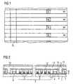
- FIG. 1shows a plan view of a carrier surface indicating the arrangement of the active areas, the bitline contacts, and the source line;
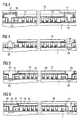
- FIG. 2shows a cross-section of an intermediate product of a first embodiment after the application of sacrificial layer
- FIG. 3shows a cross-section according to FIG. 2 of a further intermediate product after the application of a planarizing layer
- FIG. 4shows a cross-section according to FIG. 3 after the removal of the sacrificial layer
- FIG. 5shows a cross-section according to FIG. 4 after the application of the source line and a bitline via
- FIG. 6shows a cross-section according to FIG. 5 after the application of a metal layer contact-connecting the bitline via
- FIG. 7shows a cross-section according to FIG. 5 after the application of a dielectric layer, a via, and a metal layer contact-connecting the bitline via;
- FIG. 8shows a cross-section according to FIG. 6 of an embodiment encompassing a shield above the memory cell array
- FIG. 9shows a cross-section according to FIG. 8 for another embodiment having a dielectric filling in the area of the bitline via;
- FIG. 10shows a cross-section according to FIG. 9 after the application of connections to the source and shield
- FIG. 11shows a cross-section according to FIG. 8 after the application of a hardmask
- FIG. 12shows a cross-section according to FIG. 11 after the application of the metal layer.
- FIG. 1shows a plan view onto the surface of a carrier, for example a semiconductor substrate.
- the active areas AAare interrupted by insulating regions, which can be formed by shallow trench isolations.
- the bitline contacts BLare provided in a schematically shown pattern within the active areas. Parallel to the arrangement of the bitline contacts, a source line SL is provided above the carrier surface. This is the basic pattern of a memory device in a NAND architecture.
- FIG. 2shows a cross-section of an intermediate product of a first variant of the method.
- the carrier 1can be a semiconductor substrate or a semiconductor body that is provided with a layer or layer sequence of semiconductor material.
- the main surfacecan be provided with a thin oxide layer 2 .
- a memory cell array 3 of memory cell transistors 5is arranged above the carrier surface. Select transistors 4 are provided at the boundary of the array of memory cell transistors 5 .
- Each transistorhas a gate stack 6 , which can typically encompass a polysilicon layer 7 provided as gate electrode and a metal layer 8 provided for a reduction of the track resistance.
- the gate electrodecan be split into a control gate electrode, an intermediate dielectric layer, and a floating gate electrode that is provided as the storage means.
- the gate stackis electrically insulated by a top insulating layer 9 , which can be silicon nitride, for instance, and a sidewall insulating layer 10 , which can be formed by sidewall spacers of nitride, for instance.
- the metal layer 8 of the gate stacks 6can be tungsten, for example.
- a layer of a spacer material, a nitride or an oxide for example,is deposited on the surface. This can be affected by LPCVD (low-pressure chemical vapor deposition) to deposit a nitride layer of a thickness of typically 35 nm. This layer is preferably deposited conformally to the surface and is subsequently anisotropically etched to form sidewall spacers 11 to the gate stacks.
- the spacers 11fill the interspaces between the memory cell transistors 5 completely.
- an auxiliary layer 12is deposited, for example by means of TEOS (tetraethylorthosilicate).
- a sacrificial layer 13is then applied all over the surface, so that the openings between the spacers 11 are filled.
- the sacrificial layer 13can be polysilicon, especially undoped polysilicon.
- a subsequent CMP step(chemical mechanical polishing) renders a planar surface.
- a layer provided for a hardmask 14is then applied, which may especially be a nitride that is deposited by chemical vapor deposition (CVD).
- the hardmask 14is structured so that its remaining portions cover the regions of the sacrificial layer 13 that are indicated by vertical broken lines in FIG. 2 . These regions are provided for a dummy 15 of a source line and a dummy 16 of a bitline via.
- FIG. 2shows only one location of a source line and a bitline via, pluralities of source lines and bitline vias can be provided.
- FIG. 3shows a cross-section according to FIG. 2 after the patterning of the sacrificial layer 13 into the dummy 15 of the source line and the dummy 16 of the bitline via.
- the sacrificial layer 13can be etched with a standard etchant that is conventionally used to etch polysilicon. The residues of the hardmask are then removed. Tetraethylorthosilicate can then again be applied to form a further auxiliary layer 17 .
- a cover layer 18is applied, which can be nitride, for example, and which can again be deposited by LPCVD.
- planarizing layer 19which can be boronphosphorussilicate glass, for example. However, other dielectric materials may be suitable as well.
- the planarization stepcan be effected by CMP, stopping at the further auxiliary layer 17 , so that the upper surfaces of the remaining portions of the sacrificial layer are laid bare. The corresponding level is indicated with the horizontal broken line in FIG. 3 .
- FIG. 4shows the cross-section of the structure that is obtained after the removal of the dummies 15 , 16 , which are now substituted with corresponding openings.
- An implantation stepcan now be performed to produce doped regions 20 , which are provided as source/drain regions.
- Thiscan be a standard implantation of arsenic.
- both the first auxiliary layer 12 and the further auxiliary layer 17are preferably removed from the sidewalls and bottoms of the openings, before the implantation takes place.
- the thin oxide layer 2can also be removed, or it can be maintained to provide a scattering during the implantation. It has been mentioned above that this implantation can already be performed before the deposition of the sacrificial layer 13 according to FIG. 2 .
- FIG. 5shows a further intermediate product in a cross-section according to FIG. 4 .
- a thin liner 21is preferably sputtered onto the surface.
- the electrically conductive material that is provided for source line 22 and bitline via 23is applied into the openings.
- the electrically conductive materialcan be tungsten, for instance, which can be applied by MCVD (metal chemical vapor deposition).
- MCVDmetal chemical vapor deposition
- the applied materialis then planarized to form the planar surfaces shown in FIG. 5 . If a metal like tungsten is applied, the planarization can be effected by CMP, stopping on the liner 21 , or by etching the metal back in situ. It is now possible to connect the bitline via 23 separately from the source line 22 .
- FIG. 6shows a cross-section according to FIG. 5 after the formation of a recess in the source line 22 .
- a dielectric layer 24for example an oxide, is filled into the recess.
- a further CMP stepcan be performed, stopping on the liner 21 , so that a planar surface is obtained again.
- the lineris preferably removed from the upper surface by an etching step.
- a metal layer 25is applied, preferably a thin barrier layer, not shown in the figure, is sputtered onto the surface.
- the metal layer 25is then applied, for instance from tungsten, and structured into the shape that is provided for the bitlines. This can be done in a way known per se by a lithography step with subsequent etching.
- FIG. 7shows an alternative embodiment in a cross-section according to FIG. 6 .
- a dielectric layer 26is applied onto the surface.
- a via 27 of electrically conductive materialis formed in the dielectric layer 26 above the bitline via 23 , thus contact-connecting the bitline via 23 .
- a metal layer 28for example formed from tungsten, is then applied above the dielectric layer 26 , so that the via 27 is electrically connected by the metal layer 28 .
- the dielectric layer 26electrically insulates the metal layer 28 from the source line 22 .
- the other structural components of this embodimentare similar to the embodiment according to FIG. 6 .
- FIG. 8shows a further embodiment in a cross-section according to the cross-section of FIG. 6 .
- the structures of the embodiments according to FIGS. 6 and 8are similar, but the further embodiment according to FIG. 8 is additionally provided with a shield 29 that is formed from electrically conductive material.
- the shieldis produced by means of a further dummy portion of the sacrificial layer 13 shown in FIG. 2 . Additionally to the dummies of the source line and the bitline via, a section of the sacrificial layer 13 is maintained in an area covering the memory cell array 3 .
- the further manufacturing stepsare similar to the steps that have already been described.
- the electrically conductive material that is provided for the source line and the bitline viais preferably applied in the same production step to form the shield 29 also.
- the embodiment shown in FIG. 8is similar to the embodiment according to FIG. 6 , in which the source line 22 is recessed, so that the dielectric layer 24 insulating the source line 22 from the metal layer 25 can be applied. A corresponding recess is formed in the material of the shield, as shown in FIG. 8 , so that the dielectric layer 24 also insulates the shield 29 from the metal layer 25 .
- FIG. 9shows a further embodiment, in which a contact is provided to the shield 29 , but the opening of the bitline via is filled with a dielectric filling 31 .
- the openingcan be completely clad with the further auxiliary layer 17 and the cover layer 18 connection to the shield 29 is formed by a plug 30 of electrically conductive material.
- FIG. 10shows the electric connection of the source line 22 by a connection 32 to the source and of the shield by a connection 33 to the shield via the plug.
- FIG. 11shows a further embodiment similar to the embodiment according to FIG. 8 , in which use is made of a hardmask 34 , which can be nitride, for example.
- the hardmask 34is preferably formed after the application of the electrically conductive material forming the source line 22 , the bitline via 23 and the shield 29 , and it is patterned, preferably by a standard lithography step, to have openings in the areas of the source line 22 , the bitline via 23 , and the shield 29 . After the patterning of the hardmask 34 , the source line 22 and the shield 29 are recessed and the dielectric layer 24 is applied in the manner shown in FIG. 11 .
- the dielectric layer 24can be an oxide that is deposited through the openings of the hardmask 34 into the recessed regions above the electrically conductive material.
- FIG. 12shows the cross-section according to FIG. 11 after the application of the metal layer 25 .
- the metal layer 25can be tungsten that is applied onto a previously sputtered barrier layer.
- the barrier layeris extremely thin and not shown in FIG. 12 .
- the metal layer 25is then structured into the strips of bitlines.
Landscapes
- Engineering & Computer Science (AREA)
- Microelectronics & Electronic Packaging (AREA)
- Semiconductor Memories (AREA)
- Internal Circuitry In Semiconductor Integrated Circuit Devices (AREA)
Abstract
Description
Claims (15)
Priority Applications (4)
| Application Number | Priority Date | Filing Date | Title |
|---|---|---|---|
| US11/541,404US7767567B2 (en) | 2006-09-29 | 2006-09-29 | Method of forming a semiconductor memory device and semiconductor memory device |
| DE102006048877ADE102006048877B8 (en) | 2006-09-29 | 2006-10-16 | Method for producing a semiconductor memory component and semiconductor memory component |
| TW096132149ATW200818475A (en) | 2006-09-29 | 2007-08-29 | Method of production of a semiconductor memory device and semiconductor memory device |
| CNA2007101520215ACN101154634A (en) | 2006-09-29 | 2007-09-26 | Method of forming a semiconductor memory device and semiconductor memory device |
Applications Claiming Priority (1)
| Application Number | Priority Date | Filing Date | Title |
|---|---|---|---|
| US11/541,404US7767567B2 (en) | 2006-09-29 | 2006-09-29 | Method of forming a semiconductor memory device and semiconductor memory device |
Publications (2)
| Publication Number | Publication Date |
|---|---|
| US20080096352A1 US20080096352A1 (en) | 2008-04-24 |
| US7767567B2true US7767567B2 (en) | 2010-08-03 |
Family
ID=39256185
Family Applications (1)
| Application Number | Title | Priority Date | Filing Date |
|---|---|---|---|
| US11/541,404Expired - Fee RelatedUS7767567B2 (en) | 2006-09-29 | 2006-09-29 | Method of forming a semiconductor memory device and semiconductor memory device |
Country Status (4)
| Country | Link |
|---|---|
| US (1) | US7767567B2 (en) |
| CN (1) | CN101154634A (en) |
| DE (1) | DE102006048877B8 (en) |
| TW (1) | TW200818475A (en) |
Families Citing this family (4)
| Publication number | Priority date | Publication date | Assignee | Title |
|---|---|---|---|---|
| US20090292658A1 (en)* | 2008-05-23 | 2009-11-26 | Searete Llc, A Limited Liability Corporation Of The State Of Delaware | Acquisition and particular association of inference data indicative of inferred mental states of authoring users |
| DE102009026628A1 (en)* | 2009-06-02 | 2010-12-09 | Robert Bosch Gmbh | Micromechanical component and method for producing a micromechanical component |
| EP3480842A1 (en)* | 2017-11-02 | 2019-05-08 | IMEC vzw | Method for forming source/drain contacts |
| CN114256248B (en)* | 2020-09-24 | 2025-07-29 | 上海格易电子有限公司 | Semiconductor device and method for manufacturing the same |
Citations (11)
| Publication number | Priority date | Publication date | Assignee | Title |
|---|---|---|---|---|
| JPH11186528A (en) | 1997-12-25 | 1999-07-09 | Sony Corp | Nonvolatile semiconductor storing device and its manufacture |
| US20020001889A1 (en)* | 2000-06-28 | 2002-01-03 | Kim Ji-Soo | Methods for forming conductive contact body for integrated circuits using dummy dielectric layer |
| US20020020890A1 (en) | 2000-08-09 | 2002-02-21 | Josef Willer | Memory cell and production method |
| US6936885B2 (en) | 2000-01-17 | 2005-08-30 | Samsung Electronics Co., Ltd. | NAND-type flash memory devices and methods of fabricating the same |
| US20060003518A1 (en)* | 2004-06-30 | 2006-01-05 | Johann Harter | Method for fabricating field-effect transistor structures with gate electrodes with a metal layer |
| US20060033144A1 (en) | 2004-08-11 | 2006-02-16 | Micron Technology, Inc. | Non-planar flash memory array with shielded floating gates on silicon mesas |
| US20060152794A1 (en)* | 2005-01-07 | 2006-07-13 | Miradia Inc. | Method and structure for reducing parasitic influences of deflection devices on spatial light modulators |
| US20060197160A1 (en) | 2003-07-09 | 2006-09-07 | Kikuko Sugimae | Nonvolatile semiconductor memory device |
| US20070018207A1 (en)* | 2005-07-25 | 2007-01-25 | Freescale Semiconductor, Inc. | Split gate storage device including a horizontal first gate and a vertical second gate in a trench |
| US20070273954A1 (en)* | 2006-05-24 | 2007-11-29 | Texas Instruments Incorporated | Hinge assembly for a digital micromirror device |
| US20080012138A1 (en)* | 2006-07-17 | 2008-01-17 | Taiwan Semiconductor Manufacturing Company, Ltd. | One-time-programmable anti-fuse formed using damascene process |
- 2006
- 2006-09-29USUS11/541,404patent/US7767567B2/ennot_activeExpired - Fee Related
- 2006-10-16DEDE102006048877Apatent/DE102006048877B8/ennot_activeExpired - Fee Related
- 2007
- 2007-08-29TWTW096132149Apatent/TW200818475A/enunknown
- 2007-09-26CNCNA2007101520215Apatent/CN101154634A/enactivePending
Patent Citations (11)
| Publication number | Priority date | Publication date | Assignee | Title |
|---|---|---|---|---|
| JPH11186528A (en) | 1997-12-25 | 1999-07-09 | Sony Corp | Nonvolatile semiconductor storing device and its manufacture |
| US6936885B2 (en) | 2000-01-17 | 2005-08-30 | Samsung Electronics Co., Ltd. | NAND-type flash memory devices and methods of fabricating the same |
| US20020001889A1 (en)* | 2000-06-28 | 2002-01-03 | Kim Ji-Soo | Methods for forming conductive contact body for integrated circuits using dummy dielectric layer |
| US20020020890A1 (en) | 2000-08-09 | 2002-02-21 | Josef Willer | Memory cell and production method |
| US20060197160A1 (en) | 2003-07-09 | 2006-09-07 | Kikuko Sugimae | Nonvolatile semiconductor memory device |
| US20060003518A1 (en)* | 2004-06-30 | 2006-01-05 | Johann Harter | Method for fabricating field-effect transistor structures with gate electrodes with a metal layer |
| US20060033144A1 (en) | 2004-08-11 | 2006-02-16 | Micron Technology, Inc. | Non-planar flash memory array with shielded floating gates on silicon mesas |
| US20060152794A1 (en)* | 2005-01-07 | 2006-07-13 | Miradia Inc. | Method and structure for reducing parasitic influences of deflection devices on spatial light modulators |
| US20070018207A1 (en)* | 2005-07-25 | 2007-01-25 | Freescale Semiconductor, Inc. | Split gate storage device including a horizontal first gate and a vertical second gate in a trench |
| US20070273954A1 (en)* | 2006-05-24 | 2007-11-29 | Texas Instruments Incorporated | Hinge assembly for a digital micromirror device |
| US20080012138A1 (en)* | 2006-07-17 | 2008-01-17 | Taiwan Semiconductor Manufacturing Company, Ltd. | One-time-programmable anti-fuse formed using damascene process |
Also Published As
| Publication number | Publication date |
|---|---|
| US20080096352A1 (en) | 2008-04-24 |
| TW200818475A (en) | 2008-04-16 |
| DE102006048877B8 (en) | 2008-07-24 |
| DE102006048877B3 (en) | 2008-04-03 |
| CN101154634A (en) | 2008-04-02 |
Similar Documents
| Publication | Publication Date | Title |
|---|---|---|
| US10716755B2 (en) | Method of fabricating semiconductor device | |
| US10804363B2 (en) | Three-dimensional semiconductor memory device and method of fabricating the same | |
| KR101784695B1 (en) | Vertical memory devices and methods of manufacturing the same | |
| US11538827B2 (en) | Three-dimensional memory device with increased memory cell density | |
| US7595262B2 (en) | Manufacturing method for an integrated semiconductor structure | |
| CN109390285B (en) | Contact structure and manufacturing method thereof | |
| KR20130072516A (en) | Semiconductor device and method of manufacturing the same | |
| CN111640750B (en) | Memory and method of forming the same | |
| KR20120041312A (en) | Vertical memory devices and methods of manufacturing the same | |
| CN111180454A (en) | 3D memory device and method of manufacturing the same | |
| US7767567B2 (en) | Method of forming a semiconductor memory device and semiconductor memory device | |
| US7312489B2 (en) | Memory cell having bar-shaped storage node contact plugs and methods of fabricating same | |
| KR100599087B1 (en) | Semiconductor device and manufacturing method thereof | |
| US7825497B2 (en) | Method of manufacture of contact plug and interconnection layer of semiconductor device | |
| US7998816B2 (en) | Method for fabricating semiconductor device having vertical gate | |
| JP4921981B2 (en) | Manufacturing method of semiconductor memory cell | |
| US7320934B2 (en) | Method of forming a contact in a flash memory device | |
| US7521351B2 (en) | Method for forming a semiconductor product and semiconductor product | |
| US6750098B2 (en) | Integrated semiconductor memory and fabrication method | |
| KR20220168774A (en) | Semiconductor devices having dummy gate structures | |
| KR101120175B1 (en) | Semiconductor device and method of fabricating the same | |
| US20070246765A1 (en) | Semiconductor memory device and method for production | |
| US7109080B2 (en) | Method of forming capacitor over bitline contact | |
| KR100673209B1 (en) | Semiconductor device and manufacturing method thereof | |
| KR20170042451A (en) | Semiconductor device and method for manufacturing the same |
Legal Events
| Date | Code | Title | Description |
|---|---|---|---|
| AS | Assignment | Owner name:QIMONDA AG, GERMANY Free format text:ASSIGNMENT OF ASSIGNORS INTEREST;ASSIGNORS:WILLER, JOSEF;HOFMANN, FRANZ;REEL/FRAME:018661/0431;SIGNING DATES FROM 20061010 TO 20061023 Owner name:QIMONDA AG, GERMANY Free format text:ASSIGNMENT OF ASSIGNORS INTEREST;ASSIGNORS:WILLER, JOSEF;HOFMANN, FRANZ;SIGNING DATES FROM 20061010 TO 20061023;REEL/FRAME:018661/0431 | |
| FEPP | Fee payment procedure | Free format text:PAYOR NUMBER ASSIGNED (ORIGINAL EVENT CODE: ASPN); ENTITY STATUS OF PATENT OWNER: LARGE ENTITY | |
| FPAY | Fee payment | Year of fee payment:4 | |
| AS | Assignment | Owner name:INFINEON TECHNOLOGIES AG, GERMANY Free format text:ASSIGNMENT OF ASSIGNORS INTEREST;ASSIGNOR:QIMONDA AG;REEL/FRAME:035623/0001 Effective date:20141009 | |
| AS | Assignment | Owner name:POLARIS INNOVATIONS LIMITED, IRELAND Free format text:ASSIGNMENT OF ASSIGNORS INTEREST;ASSIGNOR:INFINEON TECHNOLOGIES AG;REEL/FRAME:037147/0487 Effective date:20150708 | |
| AS | Assignment | Owner name:POLARIS INNOVATIONS LIMITED, IRELAND Free format text:ASSIGNMENT OF ASSIGNORS INTEREST;ASSIGNOR:INFINEON TECHNOLOGIES AG;REEL/FRAME:037171/0719 Effective date:20150708 | |
| FEPP | Fee payment procedure | Free format text:MAINTENANCE FEE REMINDER MAILED (ORIGINAL EVENT CODE: REM.) | |
| LAPS | Lapse for failure to pay maintenance fees | Free format text:PATENT EXPIRED FOR FAILURE TO PAY MAINTENANCE FEES (ORIGINAL EVENT CODE: EXP.); ENTITY STATUS OF PATENT OWNER: LARGE ENTITY | |
| STCH | Information on status: patent discontinuation | Free format text:PATENT EXPIRED DUE TO NONPAYMENT OF MAINTENANCE FEES UNDER 37 CFR 1.362 | |
| FP | Lapsed due to failure to pay maintenance fee | Effective date:20180803 |