US7767262B2 - Nitrogen profile engineering in nitrided high dielectric constant films - Google Patents
Nitrogen profile engineering in nitrided high dielectric constant filmsDownload PDFInfo
- Publication number
- US7767262B2 US7767262B2US11/537,245US53724506AUS7767262B2US 7767262 B2US7767262 B2US 7767262B2US 53724506 AUS53724506 AUS 53724506AUS 7767262 B2US7767262 B2US 7767262B2
- Authority
- US
- United States
- Prior art keywords
- nitrogen
- oxygen
- substrate
- film
- containing film
- Prior art date
- Legal status (The legal status is an assumption and is not a legal conclusion. Google has not performed a legal analysis and makes no representation as to the accuracy of the status listed.)
- Expired - Fee Related, expires
Links
Images


Classifications
- C—CHEMISTRY; METALLURGY
- C23—COATING METALLIC MATERIAL; COATING MATERIAL WITH METALLIC MATERIAL; CHEMICAL SURFACE TREATMENT; DIFFUSION TREATMENT OF METALLIC MATERIAL; COATING BY VACUUM EVAPORATION, BY SPUTTERING, BY ION IMPLANTATION OR BY CHEMICAL VAPOUR DEPOSITION, IN GENERAL; INHIBITING CORROSION OF METALLIC MATERIAL OR INCRUSTATION IN GENERAL
- C23C—COATING METALLIC MATERIAL; COATING MATERIAL WITH METALLIC MATERIAL; SURFACE TREATMENT OF METALLIC MATERIAL BY DIFFUSION INTO THE SURFACE, BY CHEMICAL CONVERSION OR SUBSTITUTION; COATING BY VACUUM EVAPORATION, BY SPUTTERING, BY ION IMPLANTATION OR BY CHEMICAL VAPOUR DEPOSITION, IN GENERAL
- C23C16/00—Chemical coating by decomposition of gaseous compounds, without leaving reaction products of surface material in the coating, i.e. chemical vapour deposition [CVD] processes
- C23C16/22—Chemical coating by decomposition of gaseous compounds, without leaving reaction products of surface material in the coating, i.e. chemical vapour deposition [CVD] processes characterised by the deposition of inorganic material, other than metallic material
- C23C16/30—Deposition of compounds, mixtures or solid solutions, e.g. borides, carbides, nitrides
- C23C16/308—Oxynitrides
- C—CHEMISTRY; METALLURGY
- C23—COATING METALLIC MATERIAL; COATING MATERIAL WITH METALLIC MATERIAL; CHEMICAL SURFACE TREATMENT; DIFFUSION TREATMENT OF METALLIC MATERIAL; COATING BY VACUUM EVAPORATION, BY SPUTTERING, BY ION IMPLANTATION OR BY CHEMICAL VAPOUR DEPOSITION, IN GENERAL; INHIBITING CORROSION OF METALLIC MATERIAL OR INCRUSTATION IN GENERAL
- C23C—COATING METALLIC MATERIAL; COATING MATERIAL WITH METALLIC MATERIAL; SURFACE TREATMENT OF METALLIC MATERIAL BY DIFFUSION INTO THE SURFACE, BY CHEMICAL CONVERSION OR SUBSTITUTION; COATING BY VACUUM EVAPORATION, BY SPUTTERING, BY ION IMPLANTATION OR BY CHEMICAL VAPOUR DEPOSITION, IN GENERAL
- C23C16/00—Chemical coating by decomposition of gaseous compounds, without leaving reaction products of surface material in the coating, i.e. chemical vapour deposition [CVD] processes
- C23C16/44—Chemical coating by decomposition of gaseous compounds, without leaving reaction products of surface material in the coating, i.e. chemical vapour deposition [CVD] processes characterised by the method of coating
- C23C16/455—Chemical coating by decomposition of gaseous compounds, without leaving reaction products of surface material in the coating, i.e. chemical vapour deposition [CVD] processes characterised by the method of coating characterised by the method used for introducing gases into reaction chamber or for modifying gas flows in reaction chamber
- C23C16/45523—Pulsed gas flow or change of composition over time
- C23C16/45525—Atomic layer deposition [ALD]
- C23C16/45527—Atomic layer deposition [ALD] characterized by the ALD cycle, e.g. different flows or temperatures during half-reactions, unusual pulsing sequence, use of precursor mixtures or auxiliary reactants or activations
- C23C16/45529—Atomic layer deposition [ALD] characterized by the ALD cycle, e.g. different flows or temperatures during half-reactions, unusual pulsing sequence, use of precursor mixtures or auxiliary reactants or activations specially adapted for making a layer stack of alternating different compositions or gradient compositions
- C—CHEMISTRY; METALLURGY
- C23—COATING METALLIC MATERIAL; COATING MATERIAL WITH METALLIC MATERIAL; CHEMICAL SURFACE TREATMENT; DIFFUSION TREATMENT OF METALLIC MATERIAL; COATING BY VACUUM EVAPORATION, BY SPUTTERING, BY ION IMPLANTATION OR BY CHEMICAL VAPOUR DEPOSITION, IN GENERAL; INHIBITING CORROSION OF METALLIC MATERIAL OR INCRUSTATION IN GENERAL
- C23C—COATING METALLIC MATERIAL; COATING MATERIAL WITH METALLIC MATERIAL; SURFACE TREATMENT OF METALLIC MATERIAL BY DIFFUSION INTO THE SURFACE, BY CHEMICAL CONVERSION OR SUBSTITUTION; COATING BY VACUUM EVAPORATION, BY SPUTTERING, BY ION IMPLANTATION OR BY CHEMICAL VAPOUR DEPOSITION, IN GENERAL
- C23C16/00—Chemical coating by decomposition of gaseous compounds, without leaving reaction products of surface material in the coating, i.e. chemical vapour deposition [CVD] processes
- C23C16/44—Chemical coating by decomposition of gaseous compounds, without leaving reaction products of surface material in the coating, i.e. chemical vapour deposition [CVD] processes characterised by the method of coating
- C23C16/455—Chemical coating by decomposition of gaseous compounds, without leaving reaction products of surface material in the coating, i.e. chemical vapour deposition [CVD] processes characterised by the method of coating characterised by the method used for introducing gases into reaction chamber or for modifying gas flows in reaction chamber
- C23C16/45523—Pulsed gas flow or change of composition over time
- C23C16/45525—Atomic layer deposition [ALD]
- C23C16/45527—Atomic layer deposition [ALD] characterized by the ALD cycle, e.g. different flows or temperatures during half-reactions, unusual pulsing sequence, use of precursor mixtures or auxiliary reactants or activations
- C23C16/45536—Use of plasma, radiation or electromagnetic fields
- C23C16/45542—Plasma being used non-continuously during the ALD reactions
Definitions
- the present inventionrelates to a method of forming high dielectric constant materials for semiconductor devices, and more particularly to a method of forming nitrided high dielectric constant films having a nitrogen gradient across a thickness of the films.
- SiO 2 filmsthermal silicon oxide (SiO 2 ) films, grown thermally from Si substrates, have been used as gate dielectric films in integrated circuits.
- SiONsilicon oxynitride
- Incorporation of nitrogen into SiO 2 films to form the SiON filmshas been shown to provide several advantages, including an increase in the dielectric constant (k) of the films and reduced boron penetration through the films.
- kdielectric constant
- high-dielectric constant (high-k) materialsare being implemented as gate dielectric films to replace or supplement SiO 2 and SiON films.
- high-k dielectric materials under evaluationsuffer from various problems, such as film crystallization during anneals, growth of interfacial layers during film deposition and further processing, high density of interface traps, reduced channel mobility, reaction with poly-silicon gates, and Fermi level pinning with metal gates.
- high-k dielectric materialshave dielectric constants that are lower than is desired for many advanced semiconductor devices. Additionally, the dielectric constant of the high-k dielectric materials is lowered by the presence of an interfacial layer formed between the high-k dielectric material and the underlying substrate.
- Nitrogen-incorporation into high-k dielectric materialsmay reduce formation of the interfacial layer between the high-k dielectric material and the underlying substrate and may further reduce dopant penetration into the high-k dielectric material. Nitrogen-incorporation into high-k dielectric materials is commonly performed by post-deposition plasma processing but this can be more difficult than for conventional silicon-based dielectric materials and may cause plasma damage of the high-k dielectric material.
- Embodiments of the inventionprovide a method for forming nitrided high-k films having a nitrogen gradient across a thickness of the films.
- the nitrided high-k filmsmay be deposited by atomic layer deposition (ALD) or plasma-enhanced ALD (PEALD).
- ALDatomic layer deposition
- PEALDplasma-enhanced ALD
- the nitrided high-k filmsmay be used in advanced semiconductor devices that include capacitors and transistors.
- the methodincludes disposing a substrate in a process chamber, and forming a nitrided high-k film on the substrate by a) depositing a nitrogen-containing film, and b) depositing an oxygen-containing film, where steps a) and b) are performed, in any order, any number of times, so as to oxidize at least a portion of the thickness of the nitrogen-containing film.
- the nitrogen-containing film and the oxygen-containing filmcontain the same one or more metal elements selected from alkaline earth elements, rare earth elements, and Group IVB elements of the Periodic Table, and optionally aluminum, silicon, or aluminum and silicon.
- the nitrogen-containing film and the oxygen-containing filmeach contain hafnium, optionally one or more additional metal elements selected from alkaline earth elements, rare earth elements, and Group IVB elements of the Periodic Table, and optionally aluminum, silicon, or aluminum and silicon.
- FIG. 1Adepicts a schematic view of an ALD processing system in accordance with an embodiment of the invention
- FIG. 1Bdepicts a schematic view of a PEALD processing system in accordance with an embodiment of the invention
- FIGS. 2A-2Eschematically illustrate pulse sequences for forming nitrided high-k films according to embodiments of the invention
- FIG. 3is a process flow diagram for forming nitrided high-k films according to embodiments of the invention.
- FIGS. 4A and 4Bschematically show cross-sectional views of semiconductor devices containing nitrided high-k gate dielectric films according to embodiments of the invention.
- Nitrided dielectric materialssuch as hafnium based dielectric materials are likely to provide beneficial thermal and electrical characteristics for future high-k applications in semiconductor devices.
- Expected benefits of these dielectric materialsinclude increased thermal stability in contact with silicon or metal gate electrode material, decreased dopant diffusion, increased crystallization temperature, increased dielectric constant compared to non-nitrided materials, decreased density of interface traps, decreased threshold voltage shifts and Fermi level pinning, and improved processing characteristics.
- these dielectric material filmscan be used in applications that include future generations of high-k dielectric materials for use as both capacitor and transistor gate dielectrics.
- Embodiments of the inventionprovide a method for nitrogen profile engineering in nitrided high-k films, in particular to forming nitrided high-k films having a nitrogen gradient across a thickness of the film.
- the methodcan provide different nitrogen-profiles in the nitrided high-k films that are expected to be beneficial for device characteristics.
- the nitrided high-k filmscontain an oxygen-containing film, and a nitrogen-containing film that is at least partially oxidized during the deposition of the oxygen-containing film onto the nitrogen-containing film, or oxidized during, or after deposition of the nitrogen-containing film by additional processing within the process chamber.
- the additional processingcan include exposing the substrate to an oxygen-containing gas.
- a nitrided high-k filmcan contain an oxygen-containing film deposited onto a substrate and a nitrogen-containing film deposited onto the oxygen-containing film.
- a nitrided high-k filmcan contain nitrogen-containing film deposited onto a substrate and an oxygen-containing film deposited onto the nitrogen-containing film.
- the nitrided high-k filmcan contain a plurality of alternating oxygen-containing films and nitrogen-containing films.
- Embodiments of the inventioncan utilize ALD or PEALD processing to deposit nitrided high-k films with high film uniformity and with excellent thickness control over high aspect ratio features.
- the nitrided high-k filmscan contain one or more metal elements selected from alkaline earth elements (Be, Mg, Ca, Sr, Ba, and Ra), rare earth elements (scandium, yttrium, lanthanum of Group IIB, and the 14 lanthanides that fill the 4f electron shell), and Group IVB elements (Ti, Zr, and Hf) of the Periodic Table.
- the nitrided high-k filmsmay further contain aluminum, silicon, or both aluminum and silicon.
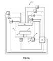
- FIG. 1Aillustrates an ALD processing system 1 for depositing nitrided high-k films on a substrate according to one embodiment of the invention.
- the ALD processing system 1includes a process chamber 10 having a substrate holder 20 configured to support a substrate 25 , upon which the nitrided high-k film is formed.
- the process chamber 10further contains an assembly 30 (e.g., a showerhead) coupled to a first process material supply system 40 , a second process material supply system 42 , a purge gas supply system 44 , an oxygen-containing gas supply system 46 , a nitrogen-containing gas supply system 48 , an aluminum-containing gas supply system 50 , and a silicon-containing gas supply system 62 .
- an assembly 30e.g., a showerhead
- the ALD processing system 1includes a substrate temperature control system 60 coupled to substrate holder 20 and configured to elevate and control the temperature of substrate 25 . Furthermore, the ALD processing system 1 includes a controller 70 that can be coupled to the process chamber 10 , substrate holder 20 , assembly 30 configured for introducing process gases into the process chamber 10 , first process material supply system 40 , second process material supply system 42 , purge gas supply system 44 , oxygen-containing gas supply system 46 , nitrogen-containing gas supply system 48 , aluminum-containing gas supply system 50 , silicon-containing gas supply system 62 , and substrate temperature control system 60 .
- controller 70can be coupled to one or more additional controllers/computers (not shown), and controller 70 can obtain setup and/or configuration information from an additional controller/computer.
- FIG. 1Asingular processing elements ( 10 , 20 , 30 , 40 , 42 , 44 , 46 , 48 , 50 , 60 , and 62 ) are shown, but this is not required for the invention.
- the ALD processing system 1can include any number of processing elements having any number of controllers associated with them in addition to independent processing elements.
- the controller 70can be used to configure any number of processing elements ( 10 , 20 , 30 , 40 , 42 , 44 , 46 , 48 , 50 , 60 , and 62 ), and the controller 70 can collect, provide, process, store, and display data from processing elements.
- the controller 70can comprise a number of applications for controlling one or more of the processing elements.
- controller 70can include a graphic user interface (GUI) component (not shown) that can provide easy to use interfaces that enable a user to monitor and/or control one or more processing elements.
- GUIgraphic user interface
- the ALD processing system 1may be configured to process 200 mm substrates, 300 mm substrates, or larger-sized substrates.
- the deposition systemmay be configured to process substrates, wafers, or LCDs regardless of their size, as would be appreciated by those skilled in the art. Therefore, while aspects of the invention will be described in connection with the processing of a semiconductor substrate, the invention is not limited solely thereto. Alternately, a batch ALD processing system capable of processing multiple substrates simultaneously may be utilized for depositing the nitrided high-k films described in the embodiments of the invention.
- the first process material supply system 40 and the second process material supply system 42are configured to alternately or simultaneously introduce metal-containing precursors containing one or more metal elements selected from alkaline earth elements, rare earth elements, and Group IVB elements of the Periodic Table.
- the alternation of the introduction of the metal-containing precursorscan be cyclical, or it may be acyclical with variable time periods between introduction of the one or more metal-containing precursors.
- each of the first process material supply system 40 and the second process material supply system 42may each be configured to alternately or simultaneously introduce a plurality of metal-containing precursors to the process chamber 10 , where the plurality of metal-containing precursors contain different metal elements selected from alkaline earth elements, rare earth elements, and Group IVB elements.
- several methodsmay be utilized for introducing the metal-containing precursors to the process chamber 10 .
- One methodincludes vaporizing precursors through the use of separate bubblers or direct liquid injection systems, or a combination thereof, and then mixing in the gas phase within or prior to introduction into the process chamber 10 .
- vaporization rate of each metal-containing precursorBy controlling the vaporization rate of each metal-containing precursor separately, a desired metal element stoichiometry can be attained within the deposited nitrided high-k film.
- Another method of delivering each metal-containing precursorincludes separately controlling two or more different liquid sources, which are then mixed prior to entering a common vaporizer. This method may be utilized when the metal-containing precursors are compatible in solution or in liquid form and they have similar vaporization characteristics.
- Liquid source precursorsmay include neat liquid metal-containing precursors, or solid or liquid metal-containing precursors that are dissolved in a compatible solvent.
- Possible compatible solventsinclude, but are not limited to, ionic liquids, hydrocarbons (aliphatic, olefins, and aromatic), amines, esters, glymes, crown ethers, ethers and polyethers. In some cases it may be possible to dissolve one or more compatible solid precursors in one or more compatible liquid precursors. It will be apparent to one skilled in the art that by controlling the relative concentration levels of the various precursors within a gas pulse, it is possible to deposit mixed metal-containing films with desired stoichiometries.
- Embodiments of the inventionsmay utilize a wide variety of different alkaline earth precursors.
- many alkaline earth precursorshave the formula: ML 1 L 2 D x where M is an alkaline earth metal element selected from the group of beryllium (Be), magnesium (Mg), calcium (Ca), strontium (Sr), and barium (Ba).
- L 1 and L 2are individual anionic ligands, and D is a neutral donor ligand where x can be 0, 1, 2, or 3.
- Each L 1 , L 2 ligandmay be individually selected from the groups of alkoxides, halides, aryloxides, amides, cyclopentadienyls, alkyls, silyls, amidinates, ⁇ -diketonates, ketoiminates, silanoates, and carboxylates.
- D ligandsmay be selected from groups of ethers, furans, pyridines, pyroles, pyrolidines, amines, crown ethers, glymes, and nitriles.
- L group alkoxidesinclude tert-butoxide, iso-propoxide, ethoxide, 1-methoxy-2,2-dimethyl-2-propionate (mmp), 1-dimethylamino-2,2′-dimethyl-propionate, amyloxide, and neo-pentoxide.
- halidesinclude fluoride, chloride, iodide, and bromide.
- aryloxidesinclude phenoxide and 2,4,6-trimethylphenoxide.
- amidesinclude bis(trimethylsilyl)amide di-tert-butylamide, and 2,2,6,6-tetramethylpiperidide (TMPD).
- cyclepentadienylsinclude cyclopentadienyl, 1-methylcyclopentadienyl, 1,2,3,4 tetramethylcyclopentadienyl, 1-ethylcyclopentadienyl, pentamethylcyclopentadienyl, 1-iso-propylcyclopentadienyl, 1-n-propylcyclopentadienyl, and 1-n-butylcyclopentadienyl.
- alkylsinclude bis(trimethylsilyl)methyl, tris(trimethylsilyl)methyl, and trimethylsilylmethyl.
- An example of a silylis trimethylsilyl.
- amidinatesinclude N,N′-di-tert-butylacetamidinate, N,N′-di-iso-propylacetamidinate, N,N′-di-isopropyl-2-tert-butylamidinate, and N,N′-di-tert-butyl-2-tert-butylamidinate.
- ⁇ -diketonatesinclude 2,2,6,6-tetramethyl-3,5-heptanedionate (THD), hexafluoro-2,4-pentanedionate (hfac), and 6,6,7,7,8,8,8-heptafluoro-2,2-dimethyl-3,5-octanedionate (FOD).
- ketoiminate2-iso-propylimino-4-pentanonate.
- silanoatesinclude tri-tert-butylsiloxide and triethylsiloxide.
- An example of a carboxylateis 2-ethylhexanoate.
- D ligandsexamples include tetrahydrofuran, diethylether, 1,2-dimethoxyethane, diglyme, triglyme, tetraglyme, 12-Crown-6, 10-Crown-4, pyridine, N-methylpyrolidine, triethylamine, trimethylamine, acetonitrile, and 2,2-dimethylpropionitrile.
- alkaline earth precursorsinclude:
- Be precursorsBe(N(SiMe 3 ) 2 ) 2 , Be(TMPD) 2 , and BeEt 2 .
- Mg precursorsMg(N(SiMe 3 ) 2 ) 2 , Mg(TMPD) 2 , Mg(PrCp) 2 , Mg(EtCp) 2 , and MgCp 2 .
- Ca precursorsCa(N(SiMe 3 ) 2 ) 2 , Ca(iPr 4 Cp) 2 , and Ca(Me 5 Cp) 2 .
- Sr precursorsBis(tert-butylacetamidinato)strontium (TBAASr), Sr—C, Sr-D, Sr(N(SiMe 3 ) 2 ) 2 , Sr(THD) 2 , Sr(THD) 2 (tetraglyme), Sr(iPr 4 Cp) 2 , Sr(iPr 3 Cp) 2 , and Sr(Me 5 Cp) 2 .
- TAAASrBis(tert-butylacetamidinato)strontium
- Ba precursorsBis(tert-butylacetamidinato)barium (TBAABa), Ba—C, Ba-D, Ba(N(SiMe 3 ) 2 ) 2 , Ba(THD) 2 , Ba(THD) 2 (tetraglyme), Ba(iPr 4 Cp) 2 , Ba(Me 5 Cp) 2 , and Ba(nPrMe 4 Cp) 2 .
- Group IVB precursorsinclude: Hf(O t Bu) 4 (hafnium tert-butoxide, HTB), Hf(NEt 2 ) 4 (tetrakis(diethylamido)hafnium, TDEAH), Hf(NEtMe) 4 (tetrakis(ethylmethylamido)hafnium, TEMAH), Hf(NMe 2 ) 4 (tetrakis(dimethylamido)hafnium, TDMAH), Zr(O t Bu) 4 (zirconium tert-butoxide, ZTB), Zr(NEt 2 ) 4 (tetrakis(diethylamido)zirconium, TDEAZ), Zr(NMeEt) 4 (tetrakis(ethylmethylamido)zirconium, TEMAZ), Zr(NMe 2 ) 4 (tetrakis(dimethylamido)zirconium, TDMAZ), Z
- Embodiments of the inventionsmay utilize a wide variety of different rare earth precursors.
- many rare earth precursorshave the formula: ML 1 L 2 L 3 D x where M is a rare earth metal element selected from the group of scandium (Sc), yttrium (Y), lutetium (Lu), lanthanum (La), cerium (Ce), praseodymium (Pr), neodymium (Nd), samarium (Sm), europium (Eu), gadolinium (Gd), terbium (Tb), dysprosium (Dy), holmium (Ho), erbium (Er), thulium (Tm), and ytterbium (Yb).
- Scscandium
- Yyttrium
- Lulutetium
- Lalanthanum
- Cecerium
- Prpraseodymium
- Ndneodymium
- Smsamarium
- Eueuropium
- L 1 , L 2 , L 3are individual anionic ligands
- Dis a neutral donor ligand where x can be 0, 1, 2, or 3.
- Each L 1 , L 2 , L 3 ligandmay be individually selected from the groups of alkoxides, halides, aryloxides, amides, cyclopentadienyls, alkyls, silyls, amidinates, ⁇ -diketonates, ketoiminates, silanoates, and carboxylates.
- D ligandsmay be selected from groups of ethers, furans, pyridines, pyroles, pyrolidines, amines, crown ethers, glymes, and nitriles.
- L groups and D ligandsare identical to those presented above for the alkaline earth precursor formula.
- rare earth precursorsinclude:
- Y precursorsY(N(SiMe 3 ) 2 ) 3 , Y(N(iPr) 2 ) 3 , Y(N(tBu)SiMe 3 ) 3 , Y(TMPD) 3 , Cp 3 Y, (MeCp) 3 Y, ((nPr)Cp) 3 Y, ((nBu)Cp) 3 Y, Y(OCMe 2 CH 2 NMe 2 ) 3 , Y(THD) 3 , Y[OOCCH(C 2 H 5 )C 4 H 9 ] 3 , Y(C 11 H 19 O 2 ) 3 CH 3 (OCH 2 CH 2 ) 3 OCH 3 , Y(CF 3 COCHCOCF 3 ) 3 , Y(OOCC 10 H 7 ) 3 , Y(OOC 10 H 19 ) 3 , and Y(O(iPr)) 3 .
- La precursorsLa(N(SiMe 3 ) 2 ) 3 , La(N(iPr) 2 ) 3 , La(N(tBu)SiMe 3 ) 3 , La(TMPD) 3 , ((iPr)Cp) 3 La, Cp 3 La, Cp 3 La(NCCH 3 ) 2 , La(Me 2 NC 2 H 4 CP) 3 , La(THD) 3 , La[OOCCH(C 2 H 5 )C 4 H 9 ] 3 , La(C 11 H 19 O 2 ) 3 .CH 3 (OCH 2 CH 2 ) 3 OCH 3 , La(C 11 H 19 O 2 ) 3 .CH 3 (OCH 2 CH 2 ) 4 OCH 3 , La(O(iPr)) 3 , La(OEt) 3 , La(acac) 3 , La(((tBu) 2 N) 2 CMe) 3 , La((iPr) 2 N) 2 CMe) 3
- Ce precursorsCe(N(SiMe 3 ) 2 ) 3 , Ce(N(iPr) 2 ) 3 , Ce(N(tBu)SiMe 3 ) 3 , Ce(TMPD) 3 , Ce(FOD) 3 , ((iPr)Cp) 3 Ce, Cp 3 Ce, Ce(Me 4 Cp) 3 , Ce(OCMe 2 CH 2 NMe 2 ) 3 , Ce(THD) 3 , Ce[OOCCH(C 2 H 5 )C 4 H 9 ] 3 , Ce(C 11 H 19 O 2 ) 3 .CH 3 (OCH 2 CH 2 ) 3 OCH 3 , Ce(C 11 H 19 O 2 ) 3 .CH 3 (OCH 2 CH 2 ) 4 OCH 3 , Ce(O(iPr)) 3 , and Ce(acac) 3 .
- Pr precursorsPr(N(SiMe 3 ) 2 ) 3 , ((iPr)Cp) 3 Pr, Cp 3 Pr, Pr(THD) 3 , Pr(FOD) 3 , (C 5 Me 4 H) 3 Pr, Pr[OOCCH(C 2 H 5 )C 4 H 9 ] 3 , Pr(C 11 H 19 O 2 ) 3 .CH 3 (OCH 2 CH 2 ) 3 OCH 3 , Pr(O(iPr)) 3 , Pr(acac) 3 , Pr(hfac) 3 , Pr(((tBu) 2 N) 2 CMe) 3 , Pr(((iPr) 2 N) 2 CMe) 3 , Pr(((tBu) 2 N) 2 C(tBu)) 3 , and Pr(((iPr) 2 N) 2 C(tBu)) 3 .
- Nd precursorsNd(N(SiMe 3 ) 2 ) 3 , Nd(N(iPr) 2 ) 3 , ((iPr)Cp) 3 Nd, Cp 3 Nd, (C 5 Me 4 H) 3 Nd, Nd(THD) 3 , Nd[OOCCH(C 2 H 5 )C 4 H 9 ] 3 , Nd(O(iPr)) 3 , Nd(acac) 3 , Nd(hfac) 3 , Nd(F 3 CC(O)CHC(O)CH 3 ) 3 , and Nd(FOD) 3 .
- Sm precursorsSm(N(SiMe 3 ) 2 ) 3 , ((iPr)Cp) 3 Sm, Cp 3 Sm, Sm(THD) 3 , Sm[OOCCH(C 2 H 5 )C 4 H 9 ] 3 , Sm(O(iPr)) 3 , Sm(acac) 3 , and (C 5 Me 5 ) 2 Sm.
- Eu precursorsEu(N(SiMe 3 ) 2 ) 3 , ((iPr)Cp) 3 Eu, Cp 3 Eu, (Me 4 Cp) 3 Eu, Eu(THD) 3 , Eu[OOCCH(C 2 H 5 )C 4 H 9 ] 3 , Eu(O(iPr)) 3 , Eu(acac) 3 , and (C 5 Me 5 ) 2 Eu.
- Gd precursorsGd(N(SiMe 3 ) 2 ) 3 , ((iPr)Cp) 3 Gd, Cp 3 Gd, Gd(THD) 3 , Gd[OOCCH(C 2 H 5 )C 4 H 9 ] 3 , Gd(O(iPr)) 3 , and Gd(acac) 3 .
- Tb precursorsTb(N(SiMe 3 ) 2 ) 3 , ((iPr)Cp) 3 Tb, Cp 3 Tb, Tb(THD) 3 , Tb[OOCCH(C 2 H 5 )C 4 H 9 ] 3 , Tb(O(iPr)) 3 , and Tb(acac) 3 .
- Dy precursorsDy(N(SiMe 3 ) 2 ) 3 , ((iPr)Cp) 3 Dy, Cp 3 Dy, Dy(THD) 3 , Dy[OOCCH(C 2 H 5 )C 4 H 9 ] 3 , Dy(O(iPr)) 3 , Dy(O 2 C(CH 2 ) 6 CH 3 ) 3 , and Dy(acac) 3 .
- Ho precursorsHo(N(SiMe 3 ) 2 ) 3 , ((iPr)Cp) 3 Ho, Cp 3 Ho, Ho(THD) 3 , Ho[OOCCH(C 2 H 5 )C 4 H 9 ] 3 , Ho(O(iPr)) 3 , and Ho(acac) 3 .
- Er precursorsEr(N(SiMe 3 ) 2 ) 3 , ((iPr)Cp) 3 Er, ((nBu)Cp) 3 Er, Cp 3 Er, Er(THD) 3 , Er[OOCCH(C 2 H 5 )C 4 H 9 ] 3 , Er(O(iPr)) 3 , and Er(acac) 3 .
- Tm precursorsTm(N(SiMe 3 ) 2 ) 3 , ((iPr)Cp) 3 Tm, Cp 3 Tm, Tm(THD) 3 , Tm[OOCCH(C 2 H 5 )C 4 H 9 ] 3 , Tm(O(iPr)) 3 , and Tm(acac) 3 .
- Yb precursorsYb(N(SiMe 3 ) 2 ) 3 , Yb(N(iPr) 2 ) 3 , ((iPr)Cp) 3 Yb, Cp 3 Yb, Yb(THD) 3 , Yb[OOCCH(C 2 H 5 )C 4 H 9 ] 3 , Yb(O(iPr)) 3 , Yb(acac) 3 , (C 5 Me 5 ) 2 Yb, Yb(hfac) 3 , and Yb(FOD) 3 .
- Lu precursorsLu(N(SiMe 3 ) 2 ) 3 , ((iPr)Cp) 3 Lu, Cp 3 Lu, Lu(THD) 3 , Lu[OOCCH(C 2 H 5 )C 4 H 9 ] 3 , Lu(O(iPr)) 3 , and Lu(acac) 3 .
- Sisilicon; Me: methyl; Et: ethyl; iPr: isopropyl; nPr: n-propyl; Bu: butyl; nBu: n-butyl; sBu: sec-butyl; iBu: iso-butyl; tBu: tert-butyl; Cp: cyclopentadienyl; THD: 2,2,6,6-tetramethyl-3,5-heptanedionate; TMPD: 2,2,6,6-tetramethylpiperidide; acac: acetylacetonate; hfac: hexafluoroacetylacetonate; and FOD: 6,6,7,7,8,8,8-heptafluoro-2,2-dimethyl-3,5-octanedionate.
- the oxygen-containing gas supply system 46is configured to introduce an oxygen-containing gas to the process chamber 10 .
- the oxygen-containing gascan include oxygen (O 2 ), water (H 2 O), or hydrogen peroxide (H 2 O 2 ), or a combination thereof, and optionally an inert gas such as Ar.
- the nitrogen-containing gas supply system 48is configured to introduce a nitrogen-containing gas to the process chamber 10 .
- the nitrogen-containing gascan include ammonia (NH 3 ), hydrazine (N 2 H 4 ), C 1 -C 10 alkylhydrazine compounds, or a combination thereof, and optionally an inert gas such as Ar.
- Common C 1 and C 2 alkylhydrazine compoundsinclude monomethyl-hydrazine (MeNHNH 2 ), 1,1-dimethyl-hydrazine (Me 2 NNH 2 ), and 1,2-dimethyl-hydrazine (MeNHNHMe).
- the oxygen-containing gas or the nitrogen-containing gascan include NO, NO 2 , or N 2 O, or a combination thereof, and optionally an inert gas such as Ar.
- Embodiments of the inventionmay utilize a wide variety of aluminum precursors for incorporating aluminum into the nitrided high-k films.
- many aluminum precursorshave the formula: AlL 1 L 2 L 3 D x where L 1 , L 2 , L 3 are individual anionic ligands, and D is a neutral donor ligand where x can be 0, 1, or 2.
- Each L 1 , L 2 , L 3 ligandmay be individually selected from the groups of alkoxides, halides, aryloxides, amides, cyclopentadienyls, alkyls, silyls, amidinates, ⁇ -diketonates, ketoiminates, silanoates, and carboxylates.
- D ligandsmay be selected from groups of ethers, furans, pyridines, pyroles, pyrolidines, amines, crown ethers, glymes, and nitriles.
- aluminum precursorsinclude: Al 2 Me 6 , Al 2 Et 6 , [Al(O(sBu)) 3 ] 4 , Al(CH 3 COCHCOCH 3 ) 3 , AlBr 3 , AlI 3 , Al(O(iPr)) 3 , [Al(NMe 2 ) 3 ] 2 , Al(iBu) 2 Cl, Al(iBu) 3 , Al(iBu) 2 H, AlEt 2 Cl, Et 3 Al 2 (O(sBu)) 3 , and Al(THD) 3 .
- Embodiments of the inventionmay utilize a wide variety of silicon precursors for incorporating silicon into the nitrided high-k films.
- silicon precursorsinclude SiH 4 , Si 2 H 6 , SiCl 3 H, SiCl 2 H 2 , SiClH 3 , Si 2 Cl 6 , ((CH 3 ) 2 N) 3 SiH (tris(dimethylamino)silane, TDMAS), and ((CH 3 ) 2 N) 2 SiH 2 (bis(dimethylamino)silane, TDMAS).
- the purge gas supply system 44is configured to introduce a purge gas to process chamber 10 .
- the introduction of purge gasmay occur between introduction of pulses of metal-containing precursors and an oxygen-containing gas, a nitrogen-containing gas, an aluminum precursor, and a silicon precursor to the process chamber 10 .
- the purge gascan comprise an inert gas, such as a noble gas (i.e., He, Ne, Ar, Kr, or Xe), nitrogen (N 2 ), or hydrogen (H 2 ).
- ALD processing system 1includes substrate temperature control system 60 coupled to the substrate holder 20 and configured to elevate and control the temperature of substrate 25 .
- Substrate temperature control system 60comprises temperature control elements, such as a cooling system including a re-circulating coolant flow that receives heat from substrate holder 20 and transfers heat to a heat exchanger system (not shown), or when heating, transfers heat from the heat exchanger system.
- the temperature control elementscan include heating/cooling elements, such as resistive heating elements, or thermo-electric heaters/coolers, which can be included in the substrate holder 20 , as well as the chamber wall of the process chamber 10 and any other component within the ALD processing system 1 .
- the substrate temperature control system 60can, for example, be configured to elevate and control the substrate temperature from room temperature to approximately 350° C. to 550° C.
- the substrate temperaturecan, for example, range from approximately 150° C. to 350° C. It is to be understood, however, that the temperature of the substrate is selected based on the desired temperature for causing deposition of a particular nitrided high-k film on the surface of a given substrate.
- substrate holder 20can include a mechanical clamping system, or an electrical clamping system, such as an electrostatic clamping system, to affix substrate 25 to an upper surface of substrate holder 20 .
- substrate holder 20can further include a substrate backside gas delivery system configured to introduce gas to the back-side of substrate 25 in order to improve the gas-gap thermal conductance between substrate 25 and substrate holder 20 .
- a substrate backside gas delivery systemconfigured to introduce gas to the back-side of substrate 25 in order to improve the gas-gap thermal conductance between substrate 25 and substrate holder 20 .
- the substrate backside gas systemcan comprise a two-zone gas distribution system, wherein the helium gas gap pressure can be independently varied between the center and the edge of substrate 25 .
- the process chamber 10is further coupled to a pressure control system 32 , including a vacuum pumping system 34 and a valve 36 , through a duct 38 , wherein the pressure control system 32 is configured to controllably evacuate the process chamber 10 to a pressure suitable for forming the nitrided high-k film on the substrate 25 .
- the vacuum pumping system 34can include a turbo-molecular vacuum pump (TMP) or a cryogenic pump capable of a pumping speed up to about 5000 liters per second (and greater) and valve 36 can include a gate valve for throttling the chamber pressure.
- a device for monitoring chamber pressure(not shown) can be coupled to the process chamber 10 .
- the pressure measuring devicecan be, for example, an absolute capacitance manometer.
- the pressure control system 32can, for example, be configured to control the process chamber pressure between about 0.1 Torr and about 100 Torr during deposition of the nitrided high-k film.
- the first process material supply system 40 , the second process material supply system 42 , the purge gas supply system 44 , the oxygen-containing gas supply system 46 , the nitrogen-containing gas supply system 48 , the aluminum-containing gas supply system 50 , and the silicon-containing gas supply system 62can include one or more pressure control devices, one or more flow control devices, one or more filters, one or more valves, and/or one or more flow sensors.
- the flow control devicescan include pneumatic driven valves, electro-mechanical (solenoidal) valves, and/or high-rate pulsed gas injection valves.
- gasesmay be sequentially and alternately pulsed into the process chamber 10 , where the length of each gas pulse can, for example, be between about 0.1 sec and about 100 sec.
- the length of each gas pulsecan be between about 1 sec and about 10 sec.
- Exemplary gas pulse lengths for metal-containing precursorscan be between 0.3 and 3 sec, for example 1 sec.
- Exemplary gas pulse lengths for aluminum precursors and silicon-precursorscan be between 0.1 and 3 sec, for example 0.3 sec.
- Exemplary gas pulse lengths for oxygen- and nitrogen-containing gasescan be between 0.3 and 3 sec, for example 1 sec.
- Exemplary purge gas pulsescan be between 1 and 20 sec, for example 3 sec.
- the controller 70can comprise a microprocessor, memory, and a digital I/O port capable of generating control voltages sufficient to communicate and activate inputs to the ALD processing system 1 as well as monitor outputs from the ALD processing system 1 .
- the controller 70may be coupled to and may exchange information with the process chamber 10 , substrate holder 20 , upper assembly 30 , first process material supply system 40 , second process material supply system 42 , purge gas supply system 44 , oxygen-containing gas supply system 46 , nitrogen-containing gas supply system 48 , aluminum-containing gas supply system 50 , silicon-containing gas supply system 62 , substrate temperature control system 60 , and pressure control system 32 .
- a program stored in the memorymay be utilized to activate the inputs to the aforementioned components of the ALD processing system 1 according to a process recipe in order to perform a deposition process.
- the controller 70is a DELL PRECISION WORKSTATION 610TM, available from Dell Corporation, Austin, Tex.
- controller 70may be implemented as a general purpose computer system that performs a portion or all of the microprocessor based processing steps of the invention in response to a processor executing one or more sequences of one or more instructions contained in a memory. Such instructions may be read into the controller memory from another computer readable medium, such as a hard disk or a removable media drive.
- processors in a multi-processing arrangementmay also be employed as the controller microprocessor to execute the sequences of instructions contained in main memory.
- hard-wired circuitrymay be used in place of or in combination with software instructions. Thus, embodiments are not limited to any specific combination of hardware circuitry and software.
- the controller 70includes at least one computer readable medium or memory, such as the controller memory, for holding instructions programmed according to the teachings of the invention and for containing data structures, tables, records, or other data that may be necessary to implement the present invention.
- Examples of computer readable mediaare compact discs, hard disks, floppy disks, tape, magneto-optical disks, PROMs (EPROM, EEPROM, flash EPROM), DRAM, SRAM, SDRAM, or any other magnetic medium, compact discs (e.g., CD-ROM), or any other optical medium, punch cards, paper tape, or other physical medium with patterns of holes, a carrier wave (described below), or any other medium from which a computer can read.
- Such softwareStored on any one or on a combination of computer readable media, resides software for controlling the controller 70 , for driving a device or devices for implementing the invention, and/or for enabling the controller to interact with a human user.
- Such softwaremay include, but is not limited to, device drivers, operating systems, development tools, and applications software.
- Such computer readable mediafurther includes the computer program product of the present invention for performing all or a portion (if processing is distributed) of the processing performed in implementing the invention.
- the computer code devicesmay be any interpretable or executable code mechanism, including but not limited to scripts, interpretable programs, dynamic link libraries (DLLs), Java classes, and complete executable programs. Moreover, parts of the processing of the present invention may be distributed for better performance, reliability, and/or cost.
- Non-volatile mediaincludes, for example, optical, magnetic disks, and magneto-optical disks, such as the hard disk or the removable media drive.
- Volatile mediaincludes dynamic memory, such as the main memory.
- various forms of computer readable mediamay be involved in carrying out one or more sequences of one or more instructions to the processor of the controller 70 for execution.
- the instructionsmay initially be carried on a magnetic disk of a remote computer.
- the remote computercan load the instructions for implementing all or a portion of the present invention remotely into a dynamic memory and send the instructions over a network to the controller 70 .
- the controller 70may be locally located relative to the ALD processing system 1 , or it may be remotely located relative to the ALD processing system 1 .
- the controller 70may exchange data with the ALD processing system 1 using at least one of a direct connection, an intranet, the Internet and a wireless connection.
- the controller 70may be coupled to an intranet at, for example, a customer site (i.e., a device maker, etc.), or it may be coupled to an intranet at, for example, a vendor site (i.e., an equipment manufacturer). Additionally, for example, the controller 70 may be coupled to the Internet.
- controller 70may access, for example, the controller 70 to exchange data via at least one of a direct connection, an intranet, and the Internet.
- controller 70may exchange data with the ALD processing system 1 via a wireless connection.
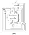
- FIG. 1Billustrates a PEALD processing system 100 for depositing nitrided high-k films on a substrate according to an embodiment of the invention.
- the PEALD processing system 100is similar to the ALD processing system 1 described in FIG. 1A , but further includes a plasma generation system configured to generate a plasma during at least a portion of the gas exposures in the process chamber 10 .
- Thisallows formation of ozone and plasma excited oxygen from an oxygen-containing gas containing O 2 , H 2 O, H 2 O 2 , or a combination thereof.
- a mixture of ozone/oxygenmay be formed.
- plasma excited nitrogenmay be formed from a nitrogen gas containing N 2 , NH 3 , or N 2 H 4 , or a combination thereof.
- plasma excited oxygen and nitrogenmay be formed from a process gas containing NO, NO 2 , and N 2 O, or a combination thereof.
- the plasma generation systemincludes a first power source 52 coupled to the process chamber 10 , and configured to couple power to gases introduced into the process chamber 10 through the assembly 31 .
- the first power source 52may be a variable power source and may include a radio frequency (RF) generator and an impedance match network, and may further include an electrode through which RF power is coupled to the plasma in process chamber 10 .
- the electrodecan be formed in the assembly 31 , and it can be configured to oppose the substrate holder 20 .
- the impedance match networkcan be configured to optimize the transfer of RF power from the RF generator to the plasma by matching the output impedance of the match network with the input impedance of the process chamber, including the electrode, and plasma. For instance, the impedance match network serves to improve the transfer of RF power to plasma in process chamber 10 by reducing the reflected power.
- Match network topologiese.g. L-type, ⁇ -type, T-type, etc.
- automatic control methodsare well known to those skilled in the art.
- the first power source 52may further include an antenna, such as an inductive coil, through which RF power is coupled to plasma in process chamber 10 .
- the antennacan, for example, include a helical or solenoidal coil, such as in an inductively coupled plasma source or helicon source, or it can, for example, include a flat coil as in a transformer coupled plasma source.
- the first power source 52may include a microwave frequency generator, and may further include a microwave antenna and microwave window through which microwave power is coupled to plasma in process chamber 10 .
- the coupling of microwave powercan be accomplished using electron cyclotron resonance (ECR) technology, or it may be employed using surface wave plasma technology, such as a slotted plane antenna (SPA), as described in U.S. Pat. No. 5,024,716.
- ECRelectron cyclotron resonance
- SPAslotted plane antenna
- the PEALD processing system 100includes a substrate bias generation system configured to generate or assist in generating a plasma (through substrate holder biasing) during at least a portion of the alternating introduction of the gases to the process chamber 10 .
- the substrate bias systemcan include a substrate power source 54 coupled to the process substrate holder 20 , and configured to couple power to the substrate 25 .
- the substrate power source 54may include a RF generator and an impedance match network, and may further include an electrode through which RF power is coupled to substrate 25 .
- the electrodecan be formed in substrate holder 20 .
- a typical frequency for the RF biascan range from about 0.1 MHz to about 100 MHz, and can be 13.56 MHz.
- RF bias systems for plasma processingare well known to those skilled in the art. Alternatively, RF power is applied to the substrate holder electrode at multiple frequencies.
- the plasma generation system and the substrate bias systemare illustrated in FIG. 1B as separate entities, they may indeed comprise one or more power sources coupled to substrate holder 20 .
- the PEALD processing system 100includes a remote plasma system 56 for providing and remotely plasma exciting an oxygen-containing gas, a nitrogen-containing gas, or a combination thereof, prior to flowing the plasma excited gas into the process chamber 10 where it is exposed to the substrate 25 .
- the remote plasma system 56can, for example, contain a microwave frequency generator.
- the process chamber pressurecan be between about 0.1 Torr and about 10 Torr, or between about 0.2 Torr and about 3 Torr.
- the remote plasma systemcan provide a mixture of ozone and O 2 to the substrate 25 .
- FIGS. 2A-2Eschematically illustrate pulse sequences for forming nitrided high-k films according to embodiments of the invention.
- Sequential and alternating pulse sequencesare used to deposit the different components (i.e., metal elements, aluminum, oxygen, nitrogen, and silicon) of the nitrided high-k films. Since ALD and PEALD processes typically deposit less than a monolayer of material per gas pulse, it is possible to form a homogenous material using separate deposition sequences of the different components of the film.
- nitrided high-k materialsmay be formed that contain one or more metal elements from alkaline earth elements, rare earth elements, and Group IVB elements.
- the nitrided high-k filmcan contain a wide variety of nitrogen-containing films and oxygen-containing films.
- Nitrogen-containing filmsmay be selected from metal nitride films, metal aluminum nitride films, metal silicon nitride films, and metal silicon aluminum nitride films.
- Oxygen-containing filmsmay be selected from metal oxide films, metal aluminate films, metal silicate films, and metal silicon aluminate films.
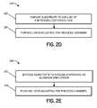
- FIG. 2Adepicts a pulse sequence 200 for depositing a metal element from a metal-containing precursor in step 202 .
- FIG. 2Bdepicts a pulse sequence 210 for depositing silicon from a silicon precursor in step 212 .
- FIG. 2Cdepicts a pulse sequence 220 for incorporating oxygen into a high-k film from exposure to an oxygen-containing gas in step 222 .
- FIG. 2Ddepicts a pulse sequence 230 for incorporating nitrogen into a high-k film from exposure to a nitrogen-containing gas in step 232 .
- FIG. 2Edepicts a pulse sequence 240 for depositing aluminum from an aluminum precursor in step 252 .
- each of the pulse sequences 200 , 210 , 220 , 230 , and 240may include a respective purge or evacuation step 204 , 214 , 224 , 234 , and 244 to remove unreacted gas or byproducts from the process chamber.
- purging stepsmay further include evacuating the process chamber during the purging.
- one or more of the purge or evacuation steps 204 , 214 , 224 , 234 , and 244may be omitted.
- FIG. 3is a process flow diagram for forming nitrided high-k films according to embodiments of the invention.
- the process flows of FIG. 3may be performed by the ALD/PEALD processing systems 1 / 101 of FIGS. 1 , 2 , or any other suitable ALD/PEALD processing systems configured to perform an ALD/PEALD process.
- the process 300begins when a substrate, such as a semiconductor substrate, is disposed in a process chamber of an ALD or PEALD processing system in step 302 .
- the substrateis exposed to a gas pulse containing a metal-containing precursor
- the process chamberis purged or evacuated to remove unreacted metal-containing precursor and any byproducts from the process chamber.
- the metal-containing precursorreacts with the surface of the heated substrate to form a chemisorbed layer less than a monolayer thick containing the metal element.
- the chemisorbed layeris less than a monolayer thick due to the large size of the metal-containing precursor compared to the size of the metal element contained in the metal-containing precursor.
- the substrateis sequentially exposed to a gas pulse of a nitrogen-containing gas, and in step 310 , the process chamber is purged or evacuated to remove unreacted nitrogen-containing gas and any byproducts from the process chamber.
- the nitrogen-containing gascan contain NH 3 , N 2 H 4 , C 1 -C 10 alkylhydrazine compounds, plasma excited nitrogen, NO, NO 2 , or N 2 O, or a combination thereof, and optionally an inert gas such as Ar.
- a nitrogen-containing film with a desired thickness on the substrateBy repeating the exposure steps 304 - 310 a predetermined number of times, as shown by the process flow arrow 320 , it is possible to deposit a nitrogen-containing film with a desired thickness on the substrate while achieving layer by layer growth of about 1 angstrom (10 ⁇ 10 m) per cycle.
- the desired film thicknesscan depend on the type of semiconductor device or device region being formed.
- a thickness of the nitrogen-containing filmcan be between about 5 angstrom and about 200 angstrom, or between about 5 angstrom and about 40 angstrom.
- step 312the substrate is exposed to a gas pulse containing a metal-containing precursor, and in step 314 , the process chamber is purged or evacuated to remove unreacted metal-containing precursor and any byproducts from the process chamber.
- step 316the substrate is sequentially exposed to a gas pulse of oxygen-containing gas, and in step 318 , the process chamber is purged or evacuated to remove unreacted oxygen-containing gas and any byproducts from the process chamber.
- the oxygen-containing gascan include O 2 , H 2 O, H 2 O 2 , ozone, plasma excited oxygen, NO, NO 2 , or N 2 O, or a combination thereof, and optionally an inert gas such as Ar.
- the exposure steps 312 - 318may be repeated a predetermined number of times, as shown by the process flow arrow 322 , to deposit an oxygen-containing film with a desired thickness on the substrate.
- a thickness of the oxygen-containing filmcan be between about 5 angstrom and about 200 angstrom, or between about 5 angstrom and about 40 angstrom.
- the metal-containing precursorcan be the same in steps 304 and 312 .
- the metal-containing precursors in steps 304 and 312can have different chemical formulas but contain the same metal element.
- the metal-containing precursors in steps 304 and 312can contain different metal elements.
- the process flows 320 and 322may be repeated a predetermined number of times, as shown by the process flow arrow 324 , to form a plurality of alternating nitrogen-containing films and oxygen-containing films until the desired number of alternating films has been formed.
- the exposure steps 304 and 312may contain a plurality (i.e., at least two) of metal-containing precursors each having a different metal element.
- the gas pulses in steps 304 and 312may contain a plurality of different metal elements to be deposited on the substrate.
- the relative concentration of each metal-containing precursor in each gas pulsemay be independently controlled to tailor the composition of the resulting nitrided high-k film.
- a nitrogen-containing filmis deposited onto a substrate as shown by process flow 320 and, subsequently, an oxygen-containing film is deposited onto the nitrogen-containing film as shown by process flow 322 .
- the order of the film depositionsmay be reversed, i.e., an oxygen-containing film deposited onto a substrate and, subsequently, a nitrogen-containing film deposited onto the oxygen-containing film.
- pulse sequences 210 and 240 depicted in FIG. 2may be added to the process 300 for incorporating silicon, aluminum, or both silicon and aluminum, into the nitrided high-k film.
- pulse sequence 210may be performed after exposure steps 310 and 318 for incorporating silicon into the nitrided high-k film.
- the methodincludes disposing a substrate in a process chamber, and forming a nitrided high-k film on the substrate by a) depositing a nitrogen-containing film, and b) depositing an oxygen-containing film, where steps a) and b) are alternatingly performed, in any order, any number of times, so as to oxidize at least a portion of the thickness of the nitrogen-containing film, and where the nitrogen-containing film and the oxygen-containing film contain the same one or more metal elements selected from alkaline earth elements, rare earth elements, and Group IVB elements of the Periodic Table, and optionally aluminum, silicon, or aluminum and silicon.
- the methodincludes disposing a substrate in a process chamber, and forming a nitrided hafnium based high-k film on the substrate by a) depositing a nitrogen-containing film, and b) depositing an oxygen-containing film, where steps a) and b) are alternatingly performed, in any order, any number of times, so as to oxidize at least a portion of the thickness of the nitrogen-containing film, and the nitrogen-containing film and the oxygen-containing film each contain hafnium, optionally one or more additional metal elements selected from alkaline earth elements, rare earth elements, and Group IVB elements of the Periodic Table, and optionally aluminum, silicon, or aluminum and silicon.
- top and bottom regionsdifferent regions across a thickness of a nitrided high-k film containing a nitrogen-containing film and an oxygen-containing film may be referred to as top and bottom regions.
- a nitrided high-k film containing an oxygen-containing film deposited onto a substrate and a nitrogen-containing film deposited onto the oxygen-containing filmmay be referred to as a top nitrided high-k film since the highest nitrogen content is in the top region of the nitrided high-k film.
- a nitrided high-k film containing a nitrogen-containing film deposited onto a substrate and an oxygen-containing film deposited onto the nitrogen-containing filmmay be referred to as a bottom nitrided high-k film since the highest nitrogen content is in the bottom region of the nitrided high-k film.
- top, middle, and bottom regionsdifferent regions across a thickness of a nitrided high-k film containing a total of three nitrogen- or oxygen-containing films.
- a top regioncan include approximately the top one third of a thickness of the nitrided high-k film
- a bottom regioncan include approximately the bottom one third of a thickness of the nitrided high-k film nearest to the underlying substrate
- a middle regioncan include approximately a third of a thickness of the nitrided high-k film between the top and bottom regions.
- a top nitrided high-k filmhas the highest nitrogen content in the top region of the nitrided high-k film.
- bottom and middle nitrided high-k filmshave the highest nitrogen content in the bottom and middle regions of the nitrided high-k films, respectively.
- a nitrided high-k filmmay be described as being bottom and middle nitrided if the nitrogen content is higher in the bottom and middle regions than in the top region.
- a nitrided high-k filmmay be described as being top and bottom nitrided if the nitrogen content is higher in the top and bottom regions than in the middle region.
- each of the top, middle, and bottom regionsneed not be construed as being limited to approximately one thirds of a thickness of the nitrided high-k film but rather may describe regions at or near the top interface, middle (bulk), and bottom interface of the nitrided high-k film, respectively.
- a nitrogen-containing filmis deposited in a desired region of the nitrided high-k film using alternating pulses of a metal-containing precursor and a nitrogen-containing gas.
- the as-deposited nitrogen-containing filmmay be a metal nitride film containing little or no oxygen or, alternately, the as-deposited nitrogen-containing film may contain substantial amounts of oxygen.
- a substantial amount of oxygenmay be incorporated into a nitrogen-containing film during deposition utilizing a metal-containing precursor containing oxygen.
- oxygenmay be incorporated into the nitrogen-containing film by exposing the substrate to an oxygen-containing gas prior to, during, or after deposition of the nitrogen-containing film.
- oxygenmay be incorporated onto the nitrogen-containing film by post-deposition processing such as exposure to an oxygen-containing gas with or without a plasma, or during formation of a gate electrode or a capping layer onto the nitrided high-k film.
- oxygenmay be incorporated into a nitrogen-containing film from an adjacent oxygen-containing film during deposition of the nitrogen-containing film onto the oxygen-containing film or during deposition of the oxygen-containing film onto the nitrogen-containing film. Due to the oxygen incorporation into the nitrogen-containing film, the final nitrogen content of the nitrogen-containing film is lower than would be obtained without an oxygen-containing film adjacent to (below, above, or both below and above) the nitrogen-containing film or without post-deposition processing.
- oxygen incorporation into the nitrogen-containing filmoxidizes at least a portion of the thickness of the nitrogen-containing film.
- the oxidized portioncontains a variable nitrogen:oxygen ratio.
- a nitrogen-containing filmis deposited onto a substrate, and an oxygen-containing film is deposited onto the nitrogen-containing film so as to oxidize at least a portion of the thickness of the nitrogen-containing film during the deposition of the oxygen-containing film.
- the nitrogen:oxygen ratio in the oxidized portion of the thickness of the nitrogen-containing filmmay increase in the direction towards the substrate.
- the nitrogen:oxygen ratio in the nitrided high-k filmmay monotonically change through the thickness thereof. In the above example, where a nitrogen-containing film is deposited onto a substrate and an oxygen-containing film is deposited onto the nitrogen-containing film, the nitrogen:oxygen ratio in the nitrided high-k film may monotonically increase through the thickness thereof.
- a hafnium based nitrogen-containing film having a thickness between about 5 angstrom and about 10 angstromis deposited onto a substrate at a substrate temperature between 150° C. and 350° C. using alternating pulses of TEMAH and ammonia.
- a hafnium based oxygen-containing film having a thickness between about 10 angstrom and about 30 angstromis deposited onto the nitrogen-containing film at a substrate temperature between 150° C. and 350° C. using alternating pulses of TEMAH and mixture of ozone/oxygen.
- the ozone concentration in the mixturemay be between 50 and 250 g/m 3 .
- Oxygen incorporation into the nitrogen-containing film during deposition of the oxygen-containing filmoxidizes at a least a portion of the thickness of the nitrogen-containing film.
- oxygen incorporationmay occur from the oxygen-containing film.
- further oxygen incorporationmay be achieved by additional ozone/oxygen exposure prior to, during, or after deposition of the nitrogen-containing film or after deposition of the oxygen-containing film.
- a first (bottom) hafnium based oxygen-containing film having a thickness between about 5 angstrom and about 10 angstromis deposited onto the substrate using alternating pulses of TEMAH and mixture of ozone/oxygen.
- a (middle) hafnium based nitrogen-containing film having a thickness between about 10 angstrom and about 20 angstrommay be deposited onto the first hafnium based oxygen-containing film using alternating pulses of TEMAH and ammonia.
- a second (top) hafnium based oxygen-containing filmis deposited onto the nitrogen-containing film.
- the second hafnium based oxygen-containing filmmay have the same thickness as the first hafnium based oxygen-containing film.
- Oxygen incorporation into the nitrogen-containing film during deposition of the second oxygen-containing filmoxidizes at least a portion of the thickness of the nitrogen-containing film.
- oxygen incorporationmay occur from the first and second oxygen-containing film.
- further oxygen incorporationmay be achieved by additional ozone/oxygen exposure prior to, during, or after deposition of the nitrogen-containing film or after deposition of the second oxygen-containing film.
- a hafnium based oxygen-containing film having a thickness between about 10 angstrom and about 30 angstromis deposited onto the substrate using alternating pulses of TEMAH and mixture of ozone/oxygen.
- a hafnium based nitrogen-containing film having a thickness between about 5 angstrom and about 10 angstromis deposited onto the hafnium based oxygen-containing film using alternating pulses of TEMAH and ammonia.
- Oxygen incorporation into the nitrogen-containing filmmay occur from the oxygen-containing film.
- further oxygen incorporationmay be achieved by additional ozone/oxygen exposure prior to, during, or after deposition of the nitrogen-containing film.
- a first (bottom) hafnium based nitrogen-containing film having a thickness between about 5 Angstrom and about 10 Angstromis deposited onto the substrate using alternating pulses of TEMAH and ammonia.
- a hafnium based oxygen-containing film having a thickness between about 10 Angstrom and about 20 Angstromis deposited onto the nitrogen-containing film using alternating pulses of TEMAH and mixture of ozone/oxygen.
- a second (top) hafnium based nitrogen-containing filmis deposited onto the oxygen-containing film.
- the second nitrogen-containing filmmay have the same thickness as the first nitrogen-containing film.
- Oxygen incorporation into the first nitrogen-containing film during deposition of the oxygen-containing filmoxidizes at a least a portion of the thickness of the first nitrogen-containing film.
- oxygen incorporation into the second nitrogen-containing filmmay occur from the oxygen-containing film.
- further oxygen incorporationmay be achieved by additional ozone/oxygen exposure prior to, during, or after deposition of the first or second nitrogen-containing films.
- a hafnium and silicon based oxygen-containing film having a thickness between about 5 angstrom and about 30 angstromis deposited onto the substrate at a substrate temperature between 150° C. and 350° C. using alternating pulses of TEMAH and mixture of ozone/oxygen, and alternating pulses of TDMAS and mixture of ozone/oxygen.
- a hafnium silicon based nitrogen-containing film having a thickness between about 5 angstrom and about 30 angstromis deposited onto the hafnium silicon based oxygen-containing film using alternating pulses of TEMAH and ammonia, and alternating pulses of TDMAS and ammonia.
- Oxygen incorporation into the nitrogen-containing filmmay occur from the oxygen-containing film.
- further oxygen incorporationmay be achieved by additional ozone/oxygen exposure prior to, during, or after deposition of the nitrogen-containing film.
- a hafnium and silicon based nitrogen-containing film having a thickness between about 5 angstrom and about 10 angstromis deposited onto a substrate at a substrate temperature between 150° C. and 350° C. using alternating pulses of TEMAH and ammonia, and alternating pulses of TDMAS and ammonia.
- a hafnium silicon based oxygen-containing film having a thickness between about 10 angstrom and about 30 angstromis deposited onto the hafnium silicon based nitrogen-containing film at a substrate temperature between 150° C. and 350° C. using alternating pulses of TEMAH and mixture of ozone/oxygen, and alternating pulses of TDMAS and ozone/oxygen.
- Oxygen incorporation into the nitrogen-containing film during deposition of the oxygen-containing filmoxidizes at a least a portion of the thickness of the nitrogen-containing film.
- oxygen incorporationmay occur from the oxygen-containing film.
- further oxygen incorporationmay be achieved by additional ozone/oxygen exposure prior to, during, or after deposition of the nitrogen-containing film or after deposition of the oxygen-containing film.
- a hafnium and strontium based nitrogen-containing film having a thickness between about 5 angstrom and about 10 angstromis deposited onto a substrate at a substrate temperature between 100° C. and 400° C. using alternating pulses of TBAASr and ammonia, and alternating pulses of TEMAH and ammonia.
- a hafnium and strontium based oxygen-containing film having a thickness between about 10 angstrom and about 30 angstromis deposited onto the hafnium and strontium based nitrogen-containing film at a substrate temperature between 100° C. and 400° C. using alternating pulses of TBAASr and mixture of ozone/oxygen, and alternating pulses of TEMAH and mixture of ozone/oxygen.
- Oxygen incorporation into the nitrogen-containing film during deposition of the oxygen-containing filmoxidizes at least a portion of the thickness of the nitrogen-containing film.
- oxygen incorporationmay occur from the oxygen-containing film.
- further oxygen incorporationmay be achieved by additional ozone/oxygen exposure prior to, during, or after deposition of the nitrogen-containing film or after deposition of the oxygen-containing film.
- a lanthanum and aluminum based nitrogen-containing film having a thickness between about 5 angstrom and about 10 angstromis deposited onto a substrate at a substrate temperature between 100° C. and 400° C. using alternating pulses of La(((iPr) 2 N) 2 CMe) 3 and ammonia, and alternating pulses of trimethylaluminum (TMA) and ammonia.
- TMAtrimethylaluminum
- a lanthanum and aluminum based oxygen-containing film having a thickness between about 10 angstrom and about 30 angstromis deposited onto the lanthanum and aluminum based nitrogen-containing film at a substrate temperature between 100° C. and 400° C.
- Oxygen incorporation into the nitrogen-containing film during deposition of the oxygen-containing filmoxidizes at a least a portion of the thickness of the nitrogen-containing film.
- oxygen incorporationmay occur from the oxygen-containing film.
- further oxygen incorporationmay be achieved by additional ozone/oxygen exposure prior to, during, or after deposition of the nitrogen-containing film or after deposition of the oxygen-containing film.
- a first (bottom) lanthanum and aluminum based oxygen-containing film having a thickness between about 5 angstrom and about 10 angstromis deposited onto the substrate using alternating pulses of La(((iPr) 2 N) 2 CMe) 3 and mixture of ozone/oxygen and alternating pulses of trimethylaluminum (TMA) and ozone/oxygen.
- a (middle) lanthanum and aluminum based nitrogen-containing film having a thickness between about 10 angstrom and about 30 angstrommay be deposited onto the first lanthanum and aluminum based oxygen-containing film using alternating pulses of La(((iPr) 2 N) 2 CMe) 3 and ammonia, and alternating pulses of trimethylaluminum (TMA) and ammonia.
- a second (top) lanthanum and aluminum oxygen-containing filmis deposited onto the nitrogen-containing film.
- the second lanthanum and aluminum based oxygen-containing filmmay have the same thickness as the first oxygen-containing film.
- Oxygen incorporation into the nitrogen-containing film during deposition of the second oxygen-containing filmoxidizes at a least a portion of the thickness of the nitrogen-containing film.
- oxygen incorporationmay occur from the first or second oxygen-containing films.
- further oxygen incorporationmay be achieved by additional ozone/oxygen exposure prior to, during, or after deposition of the nitrogen-containing film or after deposition of the first or second oxygen-containing films.
- FIGS. 4A and 4Bschematically show cross-sectional views of semiconductor devices containing nitrided high-k materials according to embodiments of the invention.
- source and drain regions of the field emission transistors (FET) 90 and 91are not shown.
- the FET 90 in FIG. 4Acontains a semiconductor substrate 92 , a nitrided high-k film 96 that serves as a gate dielectric, and a conductive gate electrode film 98 over the film 96 .
- the nitrided high-k film 96can contain any combination of nitrogen-containing films and oxygen-containing films.
- Nitrogen-containing filmsmay be selected from metal nitride films, metal aluminum nitride films, metal silicon nitride films, and metal silicon aluminum nitride films.
- Oxygen-containing filmsmay be selected from metal oxide films, metal aluminate films, metal silicate films, and metal silicon aluminate films.
- a thickness of the nitrided high-k film 96can be between about 5 and about 200 angstrom, or between about 5 and about 40 angstrom.
- the FET 90further contains a gate electrode film 98 that can, for example, be between about 5 nm and about 10 nm thick and can contain poly-Si, a metal, or a metal-containing material, including W, WN, WSi x , Al, Mo, Ta, TaN, TaSiN, HfN, HfSiN, Ti, TiN, TiSiN, Mo, MoN, Re, Pt, or Ru.
- a gate electrode film 98can, for example, be between about 5 nm and about 10 nm thick and can contain poly-Si, a metal, or a metal-containing material, including W, WN, WSi x , Al, Mo, Ta, TaN, TaSiN, HfN, HfSiN, Ti, TiN, TiSiN, Mo, MoN, Re, Pt, or Ru.
- the FET 91 in FIG. 4Bis similar to the FET 90 in FIG. 4A but further contains an interface layer 94 between the nitrided high-k film 96 and the substrate 92 .
- the interface layer 94can, for example, be an oxide layer, a nitride layer, or an oxynitride layer.
- the nitrided high-k filmscan be used in capacitors of dynamic random access memory (DRAM) devices, for example deep trench DRAM structures or stacked DRAM structures.
- DRAMdynamic random access memory
- a capacitormay be built into a high aspect ratio (depth/width) trench etched into a semiconductor substrate.
- the aspect ratio of the deep trenchcan, for example be between about 25 and about 60, which can benefit from highly conformal deposition methods such as ALD and PEALD.
Landscapes
- Chemical & Material Sciences (AREA)
- Engineering & Computer Science (AREA)
- Mechanical Engineering (AREA)
- Chemical Kinetics & Catalysis (AREA)
- General Chemical & Material Sciences (AREA)
- Materials Engineering (AREA)
- Metallurgy (AREA)
- Organic Chemistry (AREA)
- Inorganic Chemistry (AREA)
- Physics & Mathematics (AREA)
- Electromagnetism (AREA)
- Plasma & Fusion (AREA)
- Formation Of Insulating Films (AREA)
- Chemical Vapour Deposition (AREA)
Abstract
Description
ML1L2Dx
where M is an alkaline earth metal element selected from the group of beryllium (Be), magnesium (Mg), calcium (Ca), strontium (Sr), and barium (Ba). L1and L2are individual anionic ligands, and D is a neutral donor ligand where x can be 0, 1, 2, or 3. Each L1, L2ligand may be individually selected from the groups of alkoxides, halides, aryloxides, amides, cyclopentadienyls, alkyls, silyls, amidinates, β-diketonates, ketoiminates, silanoates, and carboxylates. D ligands may be selected from groups of ethers, furans, pyridines, pyroles, pyrolidines, amines, crown ethers, glymes, and nitriles.
ML1L2L3Dx
where M is a rare earth metal element selected from the group of scandium (Sc), yttrium (Y), lutetium (Lu), lanthanum (La), cerium (Ce), praseodymium (Pr), neodymium (Nd), samarium (Sm), europium (Eu), gadolinium (Gd), terbium (Tb), dysprosium (Dy), holmium (Ho), erbium (Er), thulium (Tm), and ytterbium (Yb). L1, L2, L3are individual anionic ligands, and D is a neutral donor ligand where x can be 0, 1, 2, or 3. Each L1, L2, L3ligand may be individually selected from the groups of alkoxides, halides, aryloxides, amides, cyclopentadienyls, alkyls, silyls, amidinates, β-diketonates, ketoiminates, silanoates, and carboxylates. D ligands may be selected from groups of ethers, furans, pyridines, pyroles, pyrolidines, amines, crown ethers, glymes, and nitriles.
AlL1L2L3Dx
where L1, L2, L3are individual anionic ligands, and D is a neutral donor ligand where x can be 0, 1, or 2. Each L1, L2, L3ligand may be individually selected from the groups of alkoxides, halides, aryloxides, amides, cyclopentadienyls, alkyls, silyls, amidinates, β-diketonates, ketoiminates, silanoates, and carboxylates. D ligands may be selected from groups of ethers, furans, pyridines, pyroles, pyrolidines, amines, crown ethers, glymes, and nitriles.
Claims (22)
Priority Applications (3)
| Application Number | Priority Date | Filing Date | Title |
|---|---|---|---|
| US11/537,245US7767262B2 (en) | 2006-09-29 | 2006-09-29 | Nitrogen profile engineering in nitrided high dielectric constant films |
| PCT/US2007/079681WO2008042695A2 (en) | 2006-09-29 | 2007-09-27 | Semiconductor devices containing nitrided high dielectric constant films and method of forming |
| TW096136598ATW200825204A (en) | 2006-09-29 | 2007-09-29 | Semiconductor devices containing nitrided high dielectric constant films and method of forming |
Applications Claiming Priority (1)
| Application Number | Priority Date | Filing Date | Title |
|---|---|---|---|
| US11/537,245US7767262B2 (en) | 2006-09-29 | 2006-09-29 | Nitrogen profile engineering in nitrided high dielectric constant films |
Publications (2)
| Publication Number | Publication Date |
|---|---|
| US20080081113A1 US20080081113A1 (en) | 2008-04-03 |
| US7767262B2true US7767262B2 (en) | 2010-08-03 |
Family
ID=39283719
Family Applications (1)
| Application Number | Title | Priority Date | Filing Date |
|---|---|---|---|
| US11/537,245Expired - Fee RelatedUS7767262B2 (en) | 2006-09-29 | 2006-09-29 | Nitrogen profile engineering in nitrided high dielectric constant films |
Country Status (1)
| Country | Link |
|---|---|
| US (1) | US7767262B2 (en) |
Cited By (388)
| Publication number | Priority date | Publication date | Assignee | Title |
|---|---|---|---|---|
| US20090226612A1 (en)* | 2007-10-29 | 2009-09-10 | Satoko Ogawa | Alkaline earth metal containing precursor solutions |
| US20140346650A1 (en)* | 2009-08-14 | 2014-11-27 | Asm Ip Holding B.V. | Systems and methods for thin-film deposition of metal oxides using excited nitrogen-oxygen species |
| US9324811B2 (en) | 2012-09-26 | 2016-04-26 | Asm Ip Holding B.V. | Structures and devices including a tensile-stressed silicon arsenic layer and methods of forming same |
| US9384987B2 (en) | 2012-04-04 | 2016-07-05 | Asm Ip Holding B.V. | Metal oxide protective layer for a semiconductor device |
| US9394608B2 (en) | 2009-04-06 | 2016-07-19 | Asm America, Inc. | Semiconductor processing reactor and components thereof |
| US9404587B2 (en) | 2014-04-24 | 2016-08-02 | ASM IP Holding B.V | Lockout tagout for semiconductor vacuum valve |
| US9412564B2 (en) | 2013-07-22 | 2016-08-09 | Asm Ip Holding B.V. | Semiconductor reaction chamber with plasma capabilities |
| US9447498B2 (en) | 2014-03-18 | 2016-09-20 | Asm Ip Holding B.V. | Method for performing uniform processing in gas system-sharing multiple reaction chambers |
| US9455138B1 (en) | 2015-11-10 | 2016-09-27 | Asm Ip Holding B.V. | Method for forming dielectric film in trenches by PEALD using H-containing gas |
| US9478415B2 (en) | 2015-02-13 | 2016-10-25 | Asm Ip Holding B.V. | Method for forming film having low resistance and shallow junction depth |
| US9484191B2 (en) | 2013-03-08 | 2016-11-01 | Asm Ip Holding B.V. | Pulsed remote plasma method and system |
| US9543180B2 (en) | 2014-08-01 | 2017-01-10 | Asm Ip Holding B.V. | Apparatus and method for transporting wafers between wafer carrier and process tool under vacuum |
| US9556516B2 (en) | 2013-10-09 | 2017-01-31 | ASM IP Holding B.V | Method for forming Ti-containing film by PEALD using TDMAT or TDEAT |
| US9558931B2 (en) | 2012-07-27 | 2017-01-31 | Asm Ip Holding B.V. | System and method for gas-phase sulfur passivation of a semiconductor surface |
| US9589770B2 (en) | 2013-03-08 | 2017-03-07 | Asm Ip Holding B.V. | Method and systems for in-situ formation of intermediate reactive species |
| US9605342B2 (en) | 2012-09-12 | 2017-03-28 | Asm Ip Holding B.V. | Process gas management for an inductively-coupled plasma deposition reactor |
| US9607837B1 (en) | 2015-12-21 | 2017-03-28 | Asm Ip Holding B.V. | Method for forming silicon oxide cap layer for solid state diffusion process |
| US9627221B1 (en) | 2015-12-28 | 2017-04-18 | Asm Ip Holding B.V. | Continuous process incorporating atomic layer etching |
| US9640416B2 (en) | 2012-12-26 | 2017-05-02 | Asm Ip Holding B.V. | Single-and dual-chamber module-attachable wafer-handling chamber |
| US9647114B2 (en) | 2015-08-14 | 2017-05-09 | Asm Ip Holding B.V. | Methods of forming highly p-type doped germanium tin films and structures and devices including the films |
| US9659799B2 (en) | 2012-08-28 | 2017-05-23 | Asm Ip Holding B.V. | Systems and methods for dynamic semiconductor process scheduling |
| US9657845B2 (en) | 2014-10-07 | 2017-05-23 | Asm Ip Holding B.V. | Variable conductance gas distribution apparatus and method |
| US9711345B2 (en) | 2015-08-25 | 2017-07-18 | Asm Ip Holding B.V. | Method for forming aluminum nitride-based film by PEALD |
| US9735024B2 (en) | 2015-12-28 | 2017-08-15 | Asm Ip Holding B.V. | Method of atomic layer etching using functional group-containing fluorocarbon |
| US9754779B1 (en) | 2016-02-19 | 2017-09-05 | Asm Ip Holding B.V. | Method for forming silicon nitride film selectively on sidewalls or flat surfaces of trenches |
| US9790595B2 (en) | 2013-07-12 | 2017-10-17 | Asm Ip Holding B.V. | Method and system to reduce outgassing in a reaction chamber |
| US9793148B2 (en) | 2011-06-22 | 2017-10-17 | Asm Japan K.K. | Method for positioning wafers in multiple wafer transport |
| US9793135B1 (en) | 2016-07-14 | 2017-10-17 | ASM IP Holding B.V | Method of cyclic dry etching using etchant film |
| US9793115B2 (en) | 2013-08-14 | 2017-10-17 | Asm Ip Holding B.V. | Structures and devices including germanium-tin films and methods of forming same |
| US9812320B1 (en) | 2016-07-28 | 2017-11-07 | Asm Ip Holding B.V. | Method and apparatus for filling a gap |
| US9859151B1 (en) | 2016-07-08 | 2018-01-02 | Asm Ip Holding B.V. | Selective film deposition method to form air gaps |
| US9887082B1 (en) | 2016-07-28 | 2018-02-06 | Asm Ip Holding B.V. | Method and apparatus for filling a gap |
| US9892908B2 (en) | 2011-10-28 | 2018-02-13 | Asm America, Inc. | Process feed management for semiconductor substrate processing |
| US9890456B2 (en) | 2014-08-21 | 2018-02-13 | Asm Ip Holding B.V. | Method and system for in situ formation of gas-phase compounds |
| US9891521B2 (en) | 2014-11-19 | 2018-02-13 | Asm Ip Holding B.V. | Method for depositing thin film |
| US9899291B2 (en) | 2015-07-13 | 2018-02-20 | Asm Ip Holding B.V. | Method for protecting layer by forming hydrocarbon-based extremely thin film |
| US9899405B2 (en) | 2014-12-22 | 2018-02-20 | Asm Ip Holding B.V. | Semiconductor device and manufacturing method thereof |
| US9905420B2 (en) | 2015-12-01 | 2018-02-27 | Asm Ip Holding B.V. | Methods of forming silicon germanium tin films and structures and devices including the films |
| US9909214B2 (en) | 2015-10-15 | 2018-03-06 | Asm Ip Holding B.V. | Method for depositing dielectric film in trenches by PEALD |
| US9916980B1 (en) | 2016-12-15 | 2018-03-13 | Asm Ip Holding B.V. | Method of forming a structure on a substrate |
| US9960072B2 (en) | 2015-09-29 | 2018-05-01 | Asm Ip Holding B.V. | Variable adjustment for precise matching of multiple chamber cavity housings |
| US10032628B2 (en) | 2016-05-02 | 2018-07-24 | Asm Ip Holding B.V. | Source/drain performance through conformal solid state doping |
| US10043661B2 (en) | 2015-07-13 | 2018-08-07 | Asm Ip Holding B.V. | Method for protecting layer by forming hydrocarbon-based extremely thin film |
| US10083836B2 (en) | 2015-07-24 | 2018-09-25 | Asm Ip Holding B.V. | Formation of boron-doped titanium metal films with high work function |
| US10087522B2 (en) | 2016-04-21 | 2018-10-02 | Asm Ip Holding B.V. | Deposition of metal borides |
| US10087525B2 (en) | 2015-08-04 | 2018-10-02 | Asm Ip Holding B.V. | Variable gap hard stop design |
| US10090316B2 (en) | 2016-09-01 | 2018-10-02 | Asm Ip Holding B.V. | 3D stacked multilayer semiconductor memory using doped select transistor channel |
| USD830981S1 (en) | 2017-04-07 | 2018-10-16 | Asm Ip Holding B.V. | Susceptor for semiconductor substrate processing apparatus |
| US10103040B1 (en) | 2017-03-31 | 2018-10-16 | Asm Ip Holding B.V. | Apparatus and method for manufacturing a semiconductor device |
| US10134757B2 (en) | 2016-11-07 | 2018-11-20 | Asm Ip Holding B.V. | Method of processing a substrate and a device manufactured by using the method |
| US10167557B2 (en) | 2014-03-18 | 2019-01-01 | Asm Ip Holding B.V. | Gas distribution system, reactor including the system, and methods of using the same |
| US10177025B2 (en) | 2016-07-28 | 2019-01-08 | Asm Ip Holding B.V. | Method and apparatus for filling a gap |
| US10179947B2 (en) | 2013-11-26 | 2019-01-15 | Asm Ip Holding B.V. | Method for forming conformal nitrided, oxidized, or carbonized dielectric film by atomic layer deposition |
| US10190213B2 (en) | 2016-04-21 | 2019-01-29 | Asm Ip Holding B.V. | Deposition of metal borides |
| US10211308B2 (en) | 2015-10-21 | 2019-02-19 | Asm Ip Holding B.V. | NbMC layers |
| US10229833B2 (en) | 2016-11-01 | 2019-03-12 | Asm Ip Holding B.V. | Methods for forming a transition metal nitride film on a substrate by atomic layer deposition and related semiconductor device structures |
| US10236177B1 (en) | 2017-08-22 | 2019-03-19 | ASM IP Holding B.V.. | Methods for depositing a doped germanium tin semiconductor and related semiconductor device structures |
| US10249524B2 (en) | 2017-08-09 | 2019-04-02 | Asm Ip Holding B.V. | Cassette holder assembly for a substrate cassette and holding member for use in such assembly |
| US10249577B2 (en) | 2016-05-17 | 2019-04-02 | Asm Ip Holding B.V. | Method of forming metal interconnection and method of fabricating semiconductor apparatus using the method |
| US10262859B2 (en) | 2016-03-24 | 2019-04-16 | Asm Ip Holding B.V. | Process for forming a film on a substrate using multi-port injection assemblies |
| US10269558B2 (en) | 2016-12-22 | 2019-04-23 | Asm Ip Holding B.V. | Method of forming a structure on a substrate |
| US10276355B2 (en) | 2015-03-12 | 2019-04-30 | Asm Ip Holding B.V. | Multi-zone reactor, system including the reactor, and method of using the same |
| US10283353B2 (en) | 2017-03-29 | 2019-05-07 | Asm Ip Holding B.V. | Method of reforming insulating film deposited on substrate with recess pattern |
| US10290508B1 (en) | 2017-12-05 | 2019-05-14 | Asm Ip Holding B.V. | Method for forming vertical spacers for spacer-defined patterning |
| US10312055B2 (en) | 2017-07-26 | 2019-06-04 | Asm Ip Holding B.V. | Method of depositing film by PEALD using negative bias |
| US10319588B2 (en) | 2017-10-10 | 2019-06-11 | Asm Ip Holding B.V. | Method for depositing a metal chalcogenide on a substrate by cyclical deposition |
| US10322384B2 (en) | 2015-11-09 | 2019-06-18 | Asm Ip Holding B.V. | Counter flow mixer for process chamber |
| US10340135B2 (en) | 2016-11-28 | 2019-07-02 | Asm Ip Holding B.V. | Method of topologically restricted plasma-enhanced cyclic deposition of silicon or metal nitride |
| US10343920B2 (en) | 2016-03-18 | 2019-07-09 | Asm Ip Holding B.V. | Aligned carbon nanotubes |
| US10361201B2 (en) | 2013-09-27 | 2019-07-23 | Asm Ip Holding B.V. | Semiconductor structure and device formed using selective epitaxial process |
| US10364496B2 (en) | 2011-06-27 | 2019-07-30 | Asm Ip Holding B.V. | Dual section module having shared and unshared mass flow controllers |
| US10367080B2 (en) | 2016-05-02 | 2019-07-30 | Asm Ip Holding B.V. | Method of forming a germanium oxynitride film |
| US10381219B1 (en) | 2018-10-25 | 2019-08-13 | Asm Ip Holding B.V. | Methods for forming a silicon nitride film |
| US10381226B2 (en) | 2016-07-27 | 2019-08-13 | Asm Ip Holding B.V. | Method of processing substrate |
| US10378106B2 (en) | 2008-11-14 | 2019-08-13 | Asm Ip Holding B.V. | Method of forming insulation film by modified PEALD |
| US10388509B2 (en) | 2016-06-28 | 2019-08-20 | Asm Ip Holding B.V. | Formation of epitaxial layers via dislocation filtering |
| US10388513B1 (en) | 2018-07-03 | 2019-08-20 | Asm Ip Holding B.V. | Method for depositing silicon-free carbon-containing film as gap-fill layer by pulse plasma-assisted deposition |
| US10395919B2 (en) | 2016-07-28 | 2019-08-27 | Asm Ip Holding B.V. | Method and apparatus for filling a gap |
| US10403504B2 (en) | 2017-10-05 | 2019-09-03 | Asm Ip Holding B.V. | Method for selectively depositing a metallic film on a substrate |
| US10410943B2 (en) | 2016-10-13 | 2019-09-10 | Asm Ip Holding B.V. | Method for passivating a surface of a semiconductor and related systems |
| US10435790B2 (en) | 2016-11-01 | 2019-10-08 | Asm Ip Holding B.V. | Method of subatmospheric plasma-enhanced ALD using capacitively coupled electrodes with narrow gap |
| US10446393B2 (en) | 2017-05-08 | 2019-10-15 | Asm Ip Holding B.V. | Methods for forming silicon-containing epitaxial layers and related semiconductor device structures |
| US10458018B2 (en) | 2015-06-26 | 2019-10-29 | Asm Ip Holding B.V. | Structures including metal carbide material, devices including the structures, and methods of forming same |
| US10468262B2 (en) | 2017-02-15 | 2019-11-05 | Asm Ip Holding B.V. | Methods for forming a metallic film on a substrate by a cyclical deposition and related semiconductor device structures |
| US10468251B2 (en) | 2016-02-19 | 2019-11-05 | Asm Ip Holding B.V. | Method for forming spacers using silicon nitride film for spacer-defined multiple patterning |
| US10483099B1 (en) | 2018-07-26 | 2019-11-19 | Asm Ip Holding B.V. | Method for forming thermally stable organosilicon polymer film |
| US10501866B2 (en) | 2016-03-09 | 2019-12-10 | Asm Ip Holding B.V. | Gas distribution apparatus for improved film uniformity in an epitaxial system |
| US10504742B2 (en) | 2017-05-31 | 2019-12-10 | Asm Ip Holding B.V. | Method of atomic layer etching using hydrogen plasma |
| US10510536B2 (en) | 2018-03-29 | 2019-12-17 | Asm Ip Holding B.V. | Method of depositing a co-doped polysilicon film on a surface of a substrate within a reaction chamber |
| US10529542B2 (en) | 2015-03-11 | 2020-01-07 | Asm Ip Holdings B.V. | Cross-flow reactor and method |
| US10529554B2 (en) | 2016-02-19 | 2020-01-07 | Asm Ip Holding B.V. | Method for forming silicon nitride film selectively on sidewalls or flat surfaces of trenches |
| US10529563B2 (en) | 2017-03-29 | 2020-01-07 | Asm Ip Holdings B.V. | Method for forming doped metal oxide films on a substrate by cyclical deposition and related semiconductor device structures |
| US10535516B2 (en) | 2018-02-01 | 2020-01-14 | Asm Ip Holdings B.V. | Method for depositing a semiconductor structure on a surface of a substrate and related semiconductor structures |
| US10541333B2 (en) | 2017-07-19 | 2020-01-21 | Asm Ip Holding B.V. | Method for depositing a group IV semiconductor and related semiconductor device structures |
| US10559458B1 (en) | 2018-11-26 | 2020-02-11 | Asm Ip Holding B.V. | Method of forming oxynitride film |
| US10590535B2 (en) | 2017-07-26 | 2020-03-17 | Asm Ip Holdings B.V. | Chemical treatment, deposition and/or infiltration apparatus and method for using the same |
| US10600673B2 (en) | 2015-07-07 | 2020-03-24 | Asm Ip Holding B.V. | Magnetic susceptor to baseplate seal |
| US10607895B2 (en) | 2017-09-18 | 2020-03-31 | Asm Ip Holdings B.V. | Method for forming a semiconductor device structure comprising a gate fill metal |
| US10605530B2 (en) | 2017-07-26 | 2020-03-31 | Asm Ip Holding B.V. | Assembly of a liner and a flange for a vertical furnace as well as the liner and the vertical furnace |
| USD880437S1 (en) | 2018-02-01 | 2020-04-07 | Asm Ip Holding B.V. | Gas supply plate for semiconductor manufacturing apparatus |
| US10612136B2 (en) | 2018-06-29 | 2020-04-07 | ASM IP Holding, B.V. | Temperature-controlled flange and reactor system including same |
| US10612137B2 (en) | 2016-07-08 | 2020-04-07 | Asm Ip Holdings B.V. | Organic reactants for atomic layer deposition |
| US10643904B2 (en) | 2016-11-01 | 2020-05-05 | Asm Ip Holdings B.V. | Methods for forming a semiconductor device and related semiconductor device structures |
| US10643826B2 (en) | 2016-10-26 | 2020-05-05 | Asm Ip Holdings B.V. | Methods for thermally calibrating reaction chambers |
| US10655221B2 (en) | 2017-02-09 | 2020-05-19 | Asm Ip Holding B.V. | Method for depositing oxide film by thermal ALD and PEALD |
| US10658181B2 (en) | 2018-02-20 | 2020-05-19 | Asm Ip Holding B.V. | Method of spacer-defined direct patterning in semiconductor fabrication |
| US10658205B2 (en) | 2017-09-28 | 2020-05-19 | Asm Ip Holdings B.V. | Chemical dispensing apparatus and methods for dispensing a chemical to a reaction chamber |
| US10685834B2 (en) | 2017-07-05 | 2020-06-16 | Asm Ip Holdings B.V. | Methods for forming a silicon germanium tin layer and related semiconductor device structures |
| US10683571B2 (en) | 2014-02-25 | 2020-06-16 | Asm Ip Holding B.V. | Gas supply manifold and method of supplying gases to chamber using same |
| US10692741B2 (en) | 2017-08-08 | 2020-06-23 | Asm Ip Holdings B.V. | Radiation shield |
| US10707106B2 (en) | 2011-06-06 | 2020-07-07 | Asm Ip Holding B.V. | High-throughput semiconductor-processing apparatus equipped with multiple dual-chamber modules |
| US10714335B2 (en) | 2017-04-25 | 2020-07-14 | Asm Ip Holding B.V. | Method of depositing thin film and method of manufacturing semiconductor device |
| US10714315B2 (en) | 2012-10-12 | 2020-07-14 | Asm Ip Holdings B.V. | Semiconductor reaction chamber showerhead |
| US10714385B2 (en) | 2016-07-19 | 2020-07-14 | Asm Ip Holding B.V. | Selective deposition of tungsten |
| US10714350B2 (en) | 2016-11-01 | 2020-07-14 | ASM IP Holdings, B.V. | Methods for forming a transition metal niobium nitride film on a substrate by atomic layer deposition and related semiconductor device structures |
| US10734497B2 (en) | 2017-07-18 | 2020-08-04 | Asm Ip Holding B.V. | Methods for forming a semiconductor device structure and related semiconductor device structures |
| US10734244B2 (en) | 2017-11-16 | 2020-08-04 | Asm Ip Holding B.V. | Method of processing a substrate and a device manufactured by the same |
| US10731249B2 (en) | 2018-02-15 | 2020-08-04 | Asm Ip Holding B.V. | Method of forming a transition metal containing film on a substrate by a cyclical deposition process, a method for supplying a transition metal halide compound to a reaction chamber, and related vapor deposition apparatus |
| US10755922B2 (en) | 2018-07-03 | 2020-08-25 | Asm Ip Holding B.V. | Method for depositing silicon-free carbon-containing film as gap-fill layer by pulse plasma-assisted deposition |
| US10770336B2 (en) | 2017-08-08 | 2020-09-08 | Asm Ip Holding B.V. | Substrate lift mechanism and reactor including same |
| US10767789B2 (en) | 2018-07-16 | 2020-09-08 | Asm Ip Holding B.V. | Diaphragm valves, valve components, and methods for forming valve components |
| US10770286B2 (en) | 2017-05-08 | 2020-09-08 | Asm Ip Holdings B.V. | Methods for selectively forming a silicon nitride film on a substrate and related semiconductor device structures |
| US10797133B2 (en) | 2018-06-21 | 2020-10-06 | Asm Ip Holding B.V. | Method for depositing a phosphorus doped silicon arsenide film and related semiconductor device structures |
| US10811256B2 (en) | 2018-10-16 | 2020-10-20 | Asm Ip Holding B.V. | Method for etching a carbon-containing feature |
| US10818758B2 (en) | 2018-11-16 | 2020-10-27 | Asm Ip Holding B.V. | Methods for forming a metal silicate film on a substrate in a reaction chamber and related semiconductor device structures |
| USD900036S1 (en) | 2017-08-24 | 2020-10-27 | Asm Ip Holding B.V. | Heater electrical connector and adapter |
| US10829852B2 (en) | 2018-08-16 | 2020-11-10 | Asm Ip Holding B.V. | Gas distribution device for a wafer processing apparatus |
| US10847371B2 (en) | 2018-03-27 | 2020-11-24 | Asm Ip Holding B.V. | Method of forming an electrode on a substrate and a semiconductor device structure including an electrode |
| US10847366B2 (en) | 2018-11-16 | 2020-11-24 | Asm Ip Holding B.V. | Methods for depositing a transition metal chalcogenide film on a substrate by a cyclical deposition process |
| US10844484B2 (en) | 2017-09-22 | 2020-11-24 | Asm Ip Holding B.V. | Apparatus for dispensing a vapor phase reactant to a reaction chamber and related methods |
| US10847365B2 (en) | 2018-10-11 | 2020-11-24 | Asm Ip Holding B.V. | Method of forming conformal silicon carbide film by cyclic CVD |
| US10854498B2 (en) | 2011-07-15 | 2020-12-01 | Asm Ip Holding B.V. | Wafer-supporting device and method for producing same |
| USD903477S1 (en) | 2018-01-24 | 2020-12-01 | Asm Ip Holdings B.V. | Metal clamp |
| US10858737B2 (en) | 2014-07-28 | 2020-12-08 | Asm Ip Holding B.V. | Showerhead assembly and components thereof |
| US10865475B2 (en) | 2016-04-21 | 2020-12-15 | Asm Ip Holding B.V. | Deposition of metal borides and silicides |
| US10867786B2 (en) | 2018-03-30 | 2020-12-15 | Asm Ip Holding B.V. | Substrate processing method |
| US10867788B2 (en) | 2016-12-28 | 2020-12-15 | Asm Ip Holding B.V. | Method of forming a structure on a substrate |
| US10872771B2 (en) | 2018-01-16 | 2020-12-22 | Asm Ip Holding B. V. | Method for depositing a material film on a substrate within a reaction chamber by a cyclical deposition process and related device structures |
| US10883175B2 (en) | 2018-08-09 | 2021-01-05 | Asm Ip Holding B.V. | Vertical furnace for processing substrates and a liner for use therein |
| US10886123B2 (en) | 2017-06-02 | 2021-01-05 | Asm Ip Holding B.V. | Methods for forming low temperature semiconductor layers and related semiconductor device structures |
| US10892156B2 (en) | 2017-05-08 | 2021-01-12 | Asm Ip Holding B.V. | Methods for forming a silicon nitride film on a substrate and related semiconductor device structures |
| US10896820B2 (en) | 2018-02-14 | 2021-01-19 | Asm Ip Holding B.V. | Method for depositing a ruthenium-containing film on a substrate by a cyclical deposition process |
| US10910262B2 (en) | 2017-11-16 | 2021-02-02 | Asm Ip Holding B.V. | Method of selectively depositing a capping layer structure on a semiconductor device structure |
| US10914004B2 (en) | 2018-06-29 | 2021-02-09 | Asm Ip Holding B.V. | Thin-film deposition method and manufacturing method of semiconductor device |
| US10923344B2 (en) | 2017-10-30 | 2021-02-16 | Asm Ip Holding B.V. | Methods for forming a semiconductor structure and related semiconductor structures |
| US10928731B2 (en) | 2017-09-21 | 2021-02-23 | Asm Ip Holding B.V. | Method of sequential infiltration synthesis treatment of infiltrateable material and structures and devices formed using same |
| US10934619B2 (en) | 2016-11-15 | 2021-03-02 | Asm Ip Holding B.V. | Gas supply unit and substrate processing apparatus including the gas supply unit |
| US10941490B2 (en) | 2014-10-07 | 2021-03-09 | Asm Ip Holding B.V. | Multiple temperature range susceptor, assembly, reactor and system including the susceptor, and methods of using the same |
| US10975470B2 (en) | 2018-02-23 | 2021-04-13 | Asm Ip Holding B.V. | Apparatus for detecting or monitoring for a chemical precursor in a high temperature environment |
| US11001925B2 (en) | 2016-12-19 | 2021-05-11 | Asm Ip Holding B.V. | Substrate processing apparatus |
| US11018047B2 (en) | 2018-01-25 | 2021-05-25 | Asm Ip Holding B.V. | Hybrid lift pin |
| US11015245B2 (en) | 2014-03-19 | 2021-05-25 | Asm Ip Holding B.V. | Gas-phase reactor and system having exhaust plenum and components thereof |
| US11018002B2 (en) | 2017-07-19 | 2021-05-25 | Asm Ip Holding B.V. | Method for selectively depositing a Group IV semiconductor and related semiconductor device structures |
| US11022879B2 (en) | 2017-11-24 | 2021-06-01 | Asm Ip Holding B.V. | Method of forming an enhanced unexposed photoresist layer |
| US11024523B2 (en) | 2018-09-11 | 2021-06-01 | Asm Ip Holding B.V. | Substrate processing apparatus and method |
| US11031242B2 (en) | 2018-11-07 | 2021-06-08 | Asm Ip Holding B.V. | Methods for depositing a boron doped silicon germanium film |
| USD922229S1 (en) | 2019-06-05 | 2021-06-15 | Asm Ip Holding B.V. | Device for controlling a temperature of a gas supply unit |
| US11049751B2 (en) | 2018-09-14 | 2021-06-29 | Asm Ip Holding B.V. | Cassette supply system to store and handle cassettes and processing apparatus equipped therewith |
| US11053591B2 (en) | 2018-08-06 | 2021-07-06 | Asm Ip Holding B.V. | Multi-port gas injection system and reactor system including same |
| US11056344B2 (en) | 2017-08-30 | 2021-07-06 | Asm Ip Holding B.V. | Layer forming method |
| US11056567B2 (en) | 2018-05-11 | 2021-07-06 | Asm Ip Holding B.V. | Method of forming a doped metal carbide film on a substrate and related semiconductor device structures |
| US11069510B2 (en) | 2017-08-30 | 2021-07-20 | Asm Ip Holding B.V. | Substrate processing apparatus |
| US11081345B2 (en) | 2018-02-06 | 2021-08-03 | Asm Ip Holding B.V. | Method of post-deposition treatment for silicon oxide film |
| US11087997B2 (en) | 2018-10-31 | 2021-08-10 | Asm Ip Holding B.V. | Substrate processing apparatus for processing substrates |
| US11088002B2 (en) | 2018-03-29 | 2021-08-10 | Asm Ip Holding B.V. | Substrate rack and a substrate processing system and method |
| US11114283B2 (en) | 2018-03-16 | 2021-09-07 | Asm Ip Holding B.V. | Reactor, system including the reactor, and methods of manufacturing and using same |
| US11114294B2 (en) | 2019-03-08 | 2021-09-07 | Asm Ip Holding B.V. | Structure including SiOC layer and method of forming same |
| USD930782S1 (en) | 2019-08-22 | 2021-09-14 | Asm Ip Holding B.V. | Gas distributor |
| US11127617B2 (en) | 2017-11-27 | 2021-09-21 | Asm Ip Holding B.V. | Storage device for storing wafer cassettes for use with a batch furnace |
| US11127589B2 (en) | 2019-02-01 | 2021-09-21 | Asm Ip Holding B.V. | Method of topology-selective film formation of silicon oxide |
| USD931978S1 (en) | 2019-06-27 | 2021-09-28 | Asm Ip Holding B.V. | Showerhead vacuum transport |
| US11139308B2 (en) | 2015-12-29 | 2021-10-05 | Asm Ip Holding B.V. | Atomic layer deposition of III-V compounds to form V-NAND devices |
| US11139191B2 (en) | 2017-08-09 | 2021-10-05 | Asm Ip Holding B.V. | Storage apparatus for storing cassettes for substrates and processing apparatus equipped therewith |
| US11158513B2 (en) | 2018-12-13 | 2021-10-26 | Asm Ip Holding B.V. | Methods for forming a rhenium-containing film on a substrate by a cyclical deposition process and related semiconductor device structures |
| USD935572S1 (en) | 2019-05-24 | 2021-11-09 | Asm Ip Holding B.V. | Gas channel plate |
| US11171025B2 (en) | 2019-01-22 | 2021-11-09 | Asm Ip Holding B.V. | Substrate processing device |
| US11205585B2 (en) | 2016-07-28 | 2021-12-21 | Asm Ip Holding B.V. | Substrate processing apparatus and method of operating the same |
| US11217444B2 (en) | 2018-11-30 | 2022-01-04 | Asm Ip Holding B.V. | Method for forming an ultraviolet radiation responsive metal oxide-containing film |
| US11222772B2 (en) | 2016-12-14 | 2022-01-11 | Asm Ip Holding B.V. | Substrate processing apparatus |
| USD940837S1 (en) | 2019-08-22 | 2022-01-11 | Asm Ip Holding B.V. | Electrode |
| US11227789B2 (en) | 2019-02-20 | 2022-01-18 | Asm Ip Holding B.V. | Method and apparatus for filling a recess formed within a substrate surface |
| US11227782B2 (en) | 2019-07-31 | 2022-01-18 | Asm Ip Holding B.V. | Vertical batch furnace assembly |
| US11232963B2 (en) | 2018-10-03 | 2022-01-25 | Asm Ip Holding B.V. | Substrate processing apparatus and method |
| US11230766B2 (en) | 2018-03-29 | 2022-01-25 | Asm Ip Holding B.V. | Substrate processing apparatus and method |
| US11251040B2 (en) | 2019-02-20 | 2022-02-15 | Asm Ip Holding B.V. | Cyclical deposition method including treatment step and apparatus for same |
| US11251068B2 (en) | 2018-10-19 | 2022-02-15 | Asm Ip Holding B.V. | Substrate processing apparatus and substrate processing method |
| USD944946S1 (en) | 2019-06-14 | 2022-03-01 | Asm Ip Holding B.V. | Shower plate |
| US11270899B2 (en) | 2018-06-04 | 2022-03-08 | Asm Ip Holding B.V. | Wafer handling chamber with moisture reduction |
| US11274369B2 (en) | 2018-09-11 | 2022-03-15 | Asm Ip Holding B.V. | Thin film deposition method |
| US11282698B2 (en) | 2019-07-19 | 2022-03-22 | Asm Ip Holding B.V. | Method of forming topology-controlled amorphous carbon polymer film |
| US11286562B2 (en) | 2018-06-08 | 2022-03-29 | Asm Ip Holding B.V. | Gas-phase chemical reactor and method of using same |
| US11286558B2 (en) | 2019-08-23 | 2022-03-29 | Asm Ip Holding B.V. | Methods for depositing a molybdenum nitride film on a surface of a substrate by a cyclical deposition process and related semiconductor device structures including a molybdenum nitride film |
| US11289326B2 (en) | 2019-05-07 | 2022-03-29 | Asm Ip Holding B.V. | Method for reforming amorphous carbon polymer film |
| USD947913S1 (en) | 2019-05-17 | 2022-04-05 | Asm Ip Holding B.V. | Susceptor shaft |
| US11295980B2 (en) | 2017-08-30 | 2022-04-05 | Asm Ip Holding B.V. | Methods for depositing a molybdenum metal film over a dielectric surface of a substrate by a cyclical deposition process and related semiconductor device structures |
| USD948463S1 (en) | 2018-10-24 | 2022-04-12 | Asm Ip Holding B.V. | Susceptor for semiconductor substrate supporting apparatus |
| USD949319S1 (en) | 2019-08-22 | 2022-04-19 | Asm Ip Holding B.V. | Exhaust duct |
| US11306395B2 (en) | 2017-06-28 | 2022-04-19 | Asm Ip Holding B.V. | Methods for depositing a transition metal nitride film on a substrate by atomic layer deposition and related deposition apparatus |
| US11315794B2 (en) | 2019-10-21 | 2022-04-26 | Asm Ip Holding B.V. | Apparatus and methods for selectively etching films |
| US11342216B2 (en) | 2019-02-20 | 2022-05-24 | Asm Ip Holding B.V. | Cyclical deposition method and apparatus for filling a recess formed within a substrate surface |
| US11339476B2 (en) | 2019-10-08 | 2022-05-24 | Asm Ip Holding B.V. | Substrate processing device having connection plates, substrate processing method |
| US11345999B2 (en) | 2019-06-06 | 2022-05-31 | Asm Ip Holding B.V. | Method of using a gas-phase reactor system including analyzing exhausted gas |
| US11355338B2 (en) | 2019-05-10 | 2022-06-07 | Asm Ip Holding B.V. | Method of depositing material onto a surface and structure formed according to the method |
| US11361990B2 (en) | 2018-05-28 | 2022-06-14 | Asm Ip Holding B.V. | Substrate processing method and device manufactured by using the same |
| US11374112B2 (en) | 2017-07-19 | 2022-06-28 | Asm Ip Holding B.V. | Method for depositing a group IV semiconductor and related semiconductor device structures |
| US11378337B2 (en) | 2019-03-28 | 2022-07-05 | Asm Ip Holding B.V. | Door opener and substrate processing apparatus provided therewith |
| US11390950B2 (en) | 2017-01-10 | 2022-07-19 | Asm Ip Holding B.V. | Reactor system and method to reduce residue buildup during a film deposition process |
| US11390945B2 (en) | 2019-07-03 | 2022-07-19 | Asm Ip Holding B.V. | Temperature control assembly for substrate processing apparatus and method of using same |
| US11390946B2 (en) | 2019-01-17 | 2022-07-19 | Asm Ip Holding B.V. | Methods of forming a transition metal containing film on a substrate by a cyclical deposition process |
| US11393690B2 (en) | 2018-01-19 | 2022-07-19 | Asm Ip Holding B.V. | Deposition method |
| US11401605B2 (en) | 2019-11-26 | 2022-08-02 | Asm Ip Holding B.V. | Substrate processing apparatus |
| US11414760B2 (en) | 2018-10-08 | 2022-08-16 | Asm Ip Holding B.V. | Substrate support unit, thin film deposition apparatus including the same, and substrate processing apparatus including the same |
| US11424119B2 (en) | 2019-03-08 | 2022-08-23 | Asm Ip Holding B.V. | Method for selective deposition of silicon nitride layer and structure including selectively-deposited silicon nitride layer |
| US11430640B2 (en) | 2019-07-30 | 2022-08-30 | Asm Ip Holding B.V. | Substrate processing apparatus |
| US11430674B2 (en) | 2018-08-22 | 2022-08-30 | Asm Ip Holding B.V. | Sensor array, apparatus for dispensing a vapor phase reactant to a reaction chamber and related methods |
| US11437241B2 (en) | 2020-04-08 | 2022-09-06 | Asm Ip Holding B.V. | Apparatus and methods for selectively etching silicon oxide films |
| US11443926B2 (en) | 2019-07-30 | 2022-09-13 | Asm Ip Holding B.V. | Substrate processing apparatus |
| US11447864B2 (en) | 2019-04-19 | 2022-09-20 | Asm Ip Holding B.V. | Layer forming method and apparatus |
| US11447861B2 (en) | 2016-12-15 | 2022-09-20 | Asm Ip Holding B.V. | Sequential infiltration synthesis apparatus and a method of forming a patterned structure |
| USD965044S1 (en) | 2019-08-19 | 2022-09-27 | Asm Ip Holding B.V. | Susceptor shaft |
| US11453943B2 (en) | 2016-05-25 | 2022-09-27 | Asm Ip Holding B.V. | Method for forming carbon-containing silicon/metal oxide or nitride film by ALD using silicon precursor and hydrocarbon precursor |
| USD965524S1 (en) | 2019-08-19 | 2022-10-04 | Asm Ip Holding B.V. | Susceptor support |
| US11469098B2 (en) | 2018-05-08 | 2022-10-11 | Asm Ip Holding B.V. | Methods for depositing an oxide film on a substrate by a cyclical deposition process and related device structures |
| US11473195B2 (en) | 2018-03-01 | 2022-10-18 | Asm Ip Holding B.V. | Semiconductor processing apparatus and a method for processing a substrate |
| US11476109B2 (en) | 2019-06-11 | 2022-10-18 | Asm Ip Holding B.V. | Method of forming an electronic structure using reforming gas, system for performing the method, and structure formed using the method |
| US11482412B2 (en) | 2018-01-19 | 2022-10-25 | Asm Ip Holding B.V. | Method for depositing a gap-fill layer by plasma-assisted deposition |
| US11482418B2 (en) | 2018-02-20 | 2022-10-25 | Asm Ip Holding B.V. | Substrate processing method and apparatus |
| US11482533B2 (en) | 2019-02-20 | 2022-10-25 | Asm Ip Holding B.V. | Apparatus and methods for plug fill deposition in 3-D NAND applications |
| US11488819B2 (en) | 2018-12-04 | 2022-11-01 | Asm Ip Holding B.V. | Method of cleaning substrate processing apparatus |
| US11488854B2 (en) | 2020-03-11 | 2022-11-01 | Asm Ip Holding B.V. | Substrate handling device with adjustable joints |
| US11495459B2 (en) | 2019-09-04 | 2022-11-08 | Asm Ip Holding B.V. | Methods for selective deposition using a sacrificial capping layer |
| US11492703B2 (en) | 2018-06-27 | 2022-11-08 | Asm Ip Holding B.V. | Cyclic deposition methods for forming metal-containing material and films and structures including the metal-containing material |
| US11501968B2 (en) | 2019-11-15 | 2022-11-15 | Asm Ip Holding B.V. | Method for providing a semiconductor device with silicon filled gaps |
| US11499222B2 (en) | 2018-06-27 | 2022-11-15 | Asm Ip Holding B.V. | Cyclic deposition methods for forming metal-containing material and films and structures including the metal-containing material |
| US11499226B2 (en) | 2018-11-02 | 2022-11-15 | Asm Ip Holding B.V. | Substrate supporting unit and a substrate processing device including the same |
| US11515188B2 (en) | 2019-05-16 | 2022-11-29 | Asm Ip Holding B.V. | Wafer boat handling device, vertical batch furnace and method |
| US11515187B2 (en) | 2020-05-01 | 2022-11-29 | Asm Ip Holding B.V. | Fast FOUP swapping with a FOUP handler |
| US11521851B2 (en) | 2020-02-03 | 2022-12-06 | Asm Ip Holding B.V. | Method of forming structures including a vanadium or indium layer |
| US11527403B2 (en) | 2019-12-19 | 2022-12-13 | Asm Ip Holding B.V. | Methods for filling a gap feature on a substrate surface and related semiconductor structures |
| US11527400B2 (en) | 2019-08-23 | 2022-12-13 | Asm Ip Holding B.V. | Method for depositing silicon oxide film having improved quality by peald using bis(diethylamino)silane |
| US11532757B2 (en) | 2016-10-27 | 2022-12-20 | Asm Ip Holding B.V. | Deposition of charge trapping layers |
| US11530876B2 (en) | 2020-04-24 | 2022-12-20 | Asm Ip Holding B.V. | Vertical batch furnace assembly comprising a cooling gas supply |
| US11530483B2 (en) | 2018-06-21 | 2022-12-20 | Asm Ip Holding B.V. | Substrate processing system |
| US11551925B2 (en) | 2019-04-01 | 2023-01-10 | Asm Ip Holding B.V. | Method for manufacturing a semiconductor device |
| US11551912B2 (en) | 2020-01-20 | 2023-01-10 | Asm Ip Holding B.V. | Method of forming thin film and method of modifying surface of thin film |
| USD975665S1 (en) | 2019-05-17 | 2023-01-17 | Asm Ip Holding B.V. | Susceptor shaft |
| US11557474B2 (en) | 2019-07-29 | 2023-01-17 | Asm Ip Holding B.V. | Methods for selective deposition utilizing n-type dopants and/or alternative dopants to achieve high dopant incorporation |
| US11562901B2 (en) | 2019-09-25 | 2023-01-24 | Asm Ip Holding B.V. | Substrate processing method |
| US11572620B2 (en) | 2018-11-06 | 2023-02-07 | Asm Ip Holding B.V. | Methods for selectively depositing an amorphous silicon film on a substrate |
| US11581186B2 (en) | 2016-12-15 | 2023-02-14 | Asm Ip Holding B.V. | Sequential infiltration synthesis apparatus |
| US11587814B2 (en) | 2019-07-31 | 2023-02-21 | Asm Ip Holding B.V. | Vertical batch furnace assembly |
| US11587815B2 (en) | 2019-07-31 | 2023-02-21 | Asm Ip Holding B.V. | Vertical batch furnace assembly |
| USD979506S1 (en) | 2019-08-22 | 2023-02-28 | Asm Ip Holding B.V. | Insulator |
| US11594450B2 (en) | 2019-08-22 | 2023-02-28 | Asm Ip Holding B.V. | Method for forming a structure with a hole |
| US11594600B2 (en) | 2019-11-05 | 2023-02-28 | Asm Ip Holding B.V. | Structures with doped semiconductor layers and methods and systems for forming same |
| USD980813S1 (en) | 2021-05-11 | 2023-03-14 | Asm Ip Holding B.V. | Gas flow control plate for substrate processing apparatus |
| US11605528B2 (en) | 2019-07-09 | 2023-03-14 | Asm Ip Holding B.V. | Plasma device using coaxial waveguide, and substrate treatment method |
| USD980814S1 (en) | 2021-05-11 | 2023-03-14 | Asm Ip Holding B.V. | Gas distributor for substrate processing apparatus |
| US11610774B2 (en) | 2019-10-02 | 2023-03-21 | Asm Ip Holding B.V. | Methods for forming a topographically selective silicon oxide film by a cyclical plasma-enhanced deposition process |
| USD981973S1 (en) | 2021-05-11 | 2023-03-28 | Asm Ip Holding B.V. | Reactor wall for substrate processing apparatus |
| US11615970B2 (en) | 2019-07-17 | 2023-03-28 | Asm Ip Holding B.V. | Radical assist ignition plasma system and method |
| US11626316B2 (en) | 2019-11-20 | 2023-04-11 | Asm Ip Holding B.V. | Method of depositing carbon-containing material on a surface of a substrate, structure formed using the method, and system for forming the structure |
| US11626308B2 (en) | 2020-05-13 | 2023-04-11 | Asm Ip Holding B.V. | Laser alignment fixture for a reactor system |
| US11629406B2 (en) | 2018-03-09 | 2023-04-18 | Asm Ip Holding B.V. | Semiconductor processing apparatus comprising one or more pyrometers for measuring a temperature of a substrate during transfer of the substrate |
| US11629407B2 (en) | 2019-02-22 | 2023-04-18 | Asm Ip Holding B.V. | Substrate processing apparatus and method for processing substrates |
| US11637014B2 (en) | 2019-10-17 | 2023-04-25 | Asm Ip Holding B.V. | Methods for selective deposition of doped semiconductor material |
| US11637011B2 (en) | 2019-10-16 | 2023-04-25 | Asm Ip Holding B.V. | Method of topology-selective film formation of silicon oxide |
| US11639548B2 (en) | 2019-08-21 | 2023-05-02 | Asm Ip Holding B.V. | Film-forming material mixed-gas forming device and film forming device |
| US11639811B2 (en) | 2017-11-27 | 2023-05-02 | Asm Ip Holding B.V. | Apparatus including a clean mini environment |
| US11646204B2 (en) | 2020-06-24 | 2023-05-09 | Asm Ip Holding B.V. | Method for forming a layer provided with silicon |
| US11644758B2 (en) | 2020-07-17 | 2023-05-09 | Asm Ip Holding B.V. | Structures and methods for use in photolithography |
| US11646205B2 (en) | 2019-10-29 | 2023-05-09 | Asm Ip Holding B.V. | Methods of selectively forming n-type doped material on a surface, systems for selectively forming n-type doped material, and structures formed using same |
| US11643724B2 (en) | 2019-07-18 | 2023-05-09 | Asm Ip Holding B.V. | Method of forming structures using a neutral beam |
| US11646184B2 (en) | 2019-11-29 | 2023-05-09 | Asm Ip Holding B.V. | Substrate processing apparatus |
| US11658029B2 (en) | 2018-12-14 | 2023-05-23 | Asm Ip Holding B.V. | Method of forming a device structure using selective deposition of gallium nitride and system for same |
| US11658035B2 (en) | 2020-06-30 | 2023-05-23 | Asm Ip Holding B.V. | Substrate processing method |
| US11664267B2 (en) | 2019-07-10 | 2023-05-30 | Asm Ip Holding B.V. | Substrate support assembly and substrate processing device including the same |
| US11664199B2 (en) | 2018-10-19 | 2023-05-30 | Asm Ip Holding B.V. | Substrate processing apparatus and substrate processing method |
| US11664245B2 (en) | 2019-07-16 | 2023-05-30 | Asm Ip Holding B.V. | Substrate processing device |
| US11674220B2 (en) | 2020-07-20 | 2023-06-13 | Asm Ip Holding B.V. | Method for depositing molybdenum layers using an underlayer |
| US11680839B2 (en) | 2019-08-05 | 2023-06-20 | Asm Ip Holding B.V. | Liquid level sensor for a chemical source vessel |
| US11688603B2 (en) | 2019-07-17 | 2023-06-27 | Asm Ip Holding B.V. | Methods of forming silicon germanium structures |
| USD990441S1 (en) | 2021-09-07 | 2023-06-27 | Asm Ip Holding B.V. | Gas flow control plate |
| USD990534S1 (en) | 2020-09-11 | 2023-06-27 | Asm Ip Holding B.V. | Weighted lift pin |
| US11685991B2 (en) | 2018-02-14 | 2023-06-27 | Asm Ip Holding B.V. | Method for depositing a ruthenium-containing film on a substrate by a cyclical deposition process |
| US11705333B2 (en) | 2020-05-21 | 2023-07-18 | Asm Ip Holding B.V. | Structures including multiple carbon layers and methods of forming and using same |
| US11718913B2 (en) | 2018-06-04 | 2023-08-08 | Asm Ip Holding B.V. | Gas distribution system and reactor system including same |
| US11725277B2 (en) | 2011-07-20 | 2023-08-15 | Asm Ip Holding B.V. | Pressure transmitter for a semiconductor processing environment |
| US11725280B2 (en) | 2020-08-26 | 2023-08-15 | Asm Ip Holding B.V. | Method for forming metal silicon oxide and metal silicon oxynitride layers |
| US11735422B2 (en) | 2019-10-10 | 2023-08-22 | Asm Ip Holding B.V. | Method of forming a photoresist underlayer and structure including same |
| US11742198B2 (en) | 2019-03-08 | 2023-08-29 | Asm Ip Holding B.V. | Structure including SiOCN layer and method of forming same |
| US11769682B2 (en) | 2017-08-09 | 2023-09-26 | Asm Ip Holding B.V. | Storage apparatus for storing cassettes for substrates and processing apparatus equipped therewith |
| US11767589B2 (en) | 2020-05-29 | 2023-09-26 | Asm Ip Holding B.V. | Substrate processing device |
| US11776846B2 (en) | 2020-02-07 | 2023-10-03 | Asm Ip Holding B.V. | Methods for depositing gap filling fluids and related systems and devices |
| US11781221B2 (en) | 2019-05-07 | 2023-10-10 | Asm Ip Holding B.V. | Chemical source vessel with dip tube |
| US11781243B2 (en) | 2020-02-17 | 2023-10-10 | Asm Ip Holding B.V. | Method for depositing low temperature phosphorous-doped silicon |
| US11804364B2 (en) | 2020-05-19 | 2023-10-31 | Asm Ip Holding B.V. | Substrate processing apparatus |
| US11814747B2 (en) | 2019-04-24 | 2023-11-14 | Asm Ip Holding B.V. | Gas-phase reactor system-with a reaction chamber, a solid precursor source vessel, a gas distribution system, and a flange assembly |
| US11821078B2 (en) | 2020-04-15 | 2023-11-21 | Asm Ip Holding B.V. | Method for forming precoat film and method for forming silicon-containing film |
| US11823876B2 (en) | 2019-09-05 | 2023-11-21 | Asm Ip Holding B.V. | Substrate processing apparatus |
| US11823866B2 (en) | 2020-04-02 | 2023-11-21 | Asm Ip Holding B.V. | Thin film forming method |
| US11827981B2 (en) | 2020-10-14 | 2023-11-28 | Asm Ip Holding B.V. | Method of depositing material on stepped structure |
| US11830738B2 (en) | 2020-04-03 | 2023-11-28 | Asm Ip Holding B.V. | Method for forming barrier layer and method for manufacturing semiconductor device |
| US11828707B2 (en) | 2020-02-04 | 2023-11-28 | Asm Ip Holding B.V. | Method and apparatus for transmittance measurements of large articles |
| US11830730B2 (en) | 2017-08-29 | 2023-11-28 | Asm Ip Holding B.V. | Layer forming method and apparatus |
| US11840761B2 (en) | 2019-12-04 | 2023-12-12 | Asm Ip Holding B.V. | Substrate processing apparatus |
| US11876356B2 (en) | 2020-03-11 | 2024-01-16 | Asm Ip Holding B.V. | Lockout tagout assembly and system and method of using same |
| US11873557B2 (en) | 2020-10-22 | 2024-01-16 | Asm Ip Holding B.V. | Method of depositing vanadium metal |
| USD1012873S1 (en) | 2020-09-24 | 2024-01-30 | Asm Ip Holding B.V. | Electrode for semiconductor processing apparatus |
| US11885013B2 (en) | 2019-12-17 | 2024-01-30 | Asm Ip Holding B.V. | Method of forming vanadium nitride layer and structure including the vanadium nitride layer |
| US11885020B2 (en) | 2020-12-22 | 2024-01-30 | Asm Ip Holding B.V. | Transition metal deposition method |
| US11885023B2 (en) | 2018-10-01 | 2024-01-30 | Asm Ip Holding B.V. | Substrate retaining apparatus, system including the apparatus, and method of using same |
| US11887857B2 (en) | 2020-04-24 | 2024-01-30 | Asm Ip Holding B.V. | Methods and systems for depositing a layer comprising vanadium, nitrogen, and a further element |
| US11891696B2 (en) | 2020-11-30 | 2024-02-06 | Asm Ip Holding B.V. | Injector configured for arrangement within a reaction chamber of a substrate processing apparatus |
| US11901179B2 (en) | 2020-10-28 | 2024-02-13 | Asm Ip Holding B.V. | Method and device for depositing silicon onto substrates |
| US11898243B2 (en) | 2020-04-24 | 2024-02-13 | Asm Ip Holding B.V. | Method of forming vanadium nitride-containing layer |
| US11915929B2 (en) | 2019-11-26 | 2024-02-27 | Asm Ip Holding B.V. | Methods for selectively forming a target film on a substrate comprising a first dielectric surface and a second metallic surface |
| US11923181B2 (en) | 2019-11-29 | 2024-03-05 | Asm Ip Holding B.V. | Substrate processing apparatus for minimizing the effect of a filling gas during substrate processing |
| US11929251B2 (en) | 2019-12-02 | 2024-03-12 | Asm Ip Holding B.V. | Substrate processing apparatus having electrostatic chuck and substrate processing method |
| US11946137B2 (en) | 2020-12-16 | 2024-04-02 | Asm Ip Holding B.V. | Runout and wobble measurement fixtures |
| US11959168B2 (en) | 2020-04-29 | 2024-04-16 | Asm Ip Holding B.V. | Solid source precursor vessel |
| US11961741B2 (en) | 2020-03-12 | 2024-04-16 | Asm Ip Holding B.V. | Method for fabricating layer structure having target topological profile |
| USD1023959S1 (en) | 2021-05-11 | 2024-04-23 | Asm Ip Holding B.V. | Electrode for substrate processing apparatus |
| US11967488B2 (en) | 2013-02-01 | 2024-04-23 | Asm Ip Holding B.V. | Method for treatment of deposition reactor |
| US11976359B2 (en) | 2020-01-06 | 2024-05-07 | Asm Ip Holding B.V. | Gas supply assembly, components thereof, and reactor system including same |
| US11987881B2 (en) | 2020-05-22 | 2024-05-21 | Asm Ip Holding B.V. | Apparatus for depositing thin films using hydrogen peroxide |
| US11986868B2 (en) | 2020-02-28 | 2024-05-21 | Asm Ip Holding B.V. | System dedicated for parts cleaning |
| US11996289B2 (en) | 2020-04-16 | 2024-05-28 | Asm Ip Holding B.V. | Methods of forming structures including silicon germanium and silicon layers, devices formed using the methods, and systems for performing the methods |
| US11996309B2 (en) | 2019-05-16 | 2024-05-28 | Asm Ip Holding B.V. | Wafer boat handling device, vertical batch furnace and method |
| US11993843B2 (en) | 2017-08-31 | 2024-05-28 | Asm Ip Holding B.V. | Substrate processing apparatus |
| US11996292B2 (en) | 2019-10-25 | 2024-05-28 | Asm Ip Holding B.V. | Methods for filling a gap feature on a substrate surface and related semiconductor structures |
| US11993847B2 (en) | 2020-01-08 | 2024-05-28 | Asm Ip Holding B.V. | Injector |
| US12009241B2 (en) | 2019-10-14 | 2024-06-11 | Asm Ip Holding B.V. | Vertical batch furnace assembly with detector to detect cassette |
| US12006572B2 (en) | 2019-10-08 | 2024-06-11 | Asm Ip Holding B.V. | Reactor system including a gas distribution assembly for use with activated species and method of using same |
| US12009224B2 (en) | 2020-09-29 | 2024-06-11 | Asm Ip Holding B.V. | Apparatus and method for etching metal nitrides |
| US12020934B2 (en) | 2020-07-08 | 2024-06-25 | Asm Ip Holding B.V. | Substrate processing method |
| US12027365B2 (en) | 2020-11-24 | 2024-07-02 | Asm Ip Holding B.V. | Methods for filling a gap and related systems and devices |
| US12025484B2 (en) | 2018-05-08 | 2024-07-02 | Asm Ip Holding B.V. | Thin film forming method |
| US12033885B2 (en) | 2020-01-06 | 2024-07-09 | Asm Ip Holding B.V. | Channeled lift pin |
| US12040200B2 (en) | 2017-06-20 | 2024-07-16 | Asm Ip Holding B.V. | Semiconductor processing apparatus and methods for calibrating a semiconductor processing apparatus |
| US12040177B2 (en) | 2020-08-18 | 2024-07-16 | Asm Ip Holding B.V. | Methods for forming a laminate film by cyclical plasma-enhanced deposition processes |
| US12040199B2 (en) | 2018-11-28 | 2024-07-16 | Asm Ip Holding B.V. | Substrate processing apparatus for processing substrates |
| US12051567B2 (en) | 2020-10-07 | 2024-07-30 | Asm Ip Holding B.V. | Gas supply unit and substrate processing apparatus including gas supply unit |
| US12051602B2 (en) | 2020-05-04 | 2024-07-30 | Asm Ip Holding B.V. | Substrate processing system for processing substrates with an electronics module located behind a door in a front wall of the substrate processing system |
| US12057314B2 (en) | 2020-05-15 | 2024-08-06 | Asm Ip Holding B.V. | Methods for silicon germanium uniformity control using multiple precursors |
| US12074022B2 (en) | 2020-08-27 | 2024-08-27 | Asm Ip Holding B.V. | Method and system for forming patterned structures using multiple patterning process |
| US12087586B2 (en) | 2020-04-15 | 2024-09-10 | Asm Ip Holding B.V. | Method of forming chromium nitride layer and structure including the chromium nitride layer |
| US12107005B2 (en) | 2020-10-06 | 2024-10-01 | Asm Ip Holding B.V. | Deposition method and an apparatus for depositing a silicon-containing material |
| US12106944B2 (en) | 2020-06-02 | 2024-10-01 | Asm Ip Holding B.V. | Rotating substrate support |
| US12112940B2 (en) | 2019-07-19 | 2024-10-08 | Asm Ip Holding B.V. | Method of forming topology-controlled amorphous carbon polymer film |
| US12125700B2 (en) | 2020-01-16 | 2024-10-22 | Asm Ip Holding B.V. | Method of forming high aspect ratio features |
| US12129545B2 (en) | 2020-12-22 | 2024-10-29 | Asm Ip Holding B.V. | Precursor capsule, a vessel and a method |
| US12131885B2 (en) | 2020-12-22 | 2024-10-29 | Asm Ip Holding B.V. | Plasma treatment device having matching box |
| US12148609B2 (en) | 2020-09-16 | 2024-11-19 | Asm Ip Holding B.V. | Silicon oxide deposition method |
| US12154824B2 (en) | 2020-08-14 | 2024-11-26 | Asm Ip Holding B.V. | Substrate processing method |
| US12159788B2 (en) | 2020-12-14 | 2024-12-03 | Asm Ip Holding B.V. | Method of forming structures for threshold voltage control |
| US12169361B2 (en) | 2019-07-30 | 2024-12-17 | Asm Ip Holding B.V. | Substrate processing apparatus and method |
| US12173404B2 (en) | 2020-03-17 | 2024-12-24 | Asm Ip Holding B.V. | Method of depositing epitaxial material, structure formed using the method, and system for performing the method |
| US12195852B2 (en) | 2020-11-23 | 2025-01-14 | Asm Ip Holding B.V. | Substrate processing apparatus with an injector |
| US12209308B2 (en) | 2020-11-12 | 2025-01-28 | Asm Ip Holding B.V. | Reactor and related methods |
| US12211742B2 (en) | 2020-09-10 | 2025-01-28 | Asm Ip Holding B.V. | Methods for depositing gap filling fluid |
| US12218000B2 (en) | 2020-09-25 | 2025-02-04 | Asm Ip Holding B.V. | Semiconductor processing method |
| USD1060598S1 (en) | 2021-12-03 | 2025-02-04 | Asm Ip Holding B.V. | Split showerhead cover |
| US12218269B2 (en) | 2020-02-13 | 2025-02-04 | Asm Ip Holding B.V. | Substrate processing apparatus including light receiving device and calibration method of light receiving device |
| US12217946B2 (en) | 2020-10-15 | 2025-02-04 | Asm Ip Holding B.V. | Method of manufacturing semiconductor device, and substrate treatment apparatus using ether-CAT |
| US12217954B2 (en) | 2020-08-25 | 2025-02-04 | Asm Ip Holding B.V. | Method of cleaning a surface |
| US12221357B2 (en) | 2020-04-24 | 2025-02-11 | Asm Ip Holding B.V. | Methods and apparatus for stabilizing vanadium compounds |
| US12230531B2 (en) | 2018-04-09 | 2025-02-18 | Asm Ip Holding B.V. | Substrate supporting apparatus, substrate processing apparatus including the same, and substrate processing method |
| US12243757B2 (en) | 2020-05-21 | 2025-03-04 | Asm Ip Holding B.V. | Flange and apparatus for processing substrates |
| US12241158B2 (en) | 2020-07-20 | 2025-03-04 | Asm Ip Holding B.V. | Method for forming structures including transition metal layers |
| US12243742B2 (en) | 2020-04-21 | 2025-03-04 | Asm Ip Holding B.V. | Method for processing a substrate |
| US12243747B2 (en) | 2020-04-24 | 2025-03-04 | Asm Ip Holding B.V. | Methods of forming structures including vanadium boride and vanadium phosphide layers |
| US12247286B2 (en) | 2019-08-09 | 2025-03-11 | Asm Ip Holding B.V. | Heater assembly including cooling apparatus and method of using same |
| US12252785B2 (en) | 2019-06-10 | 2025-03-18 | Asm Ip Holding B.V. | Method for cleaning quartz epitaxial chambers |
| US12255053B2 (en) | 2020-12-10 | 2025-03-18 | Asm Ip Holding B.V. | Methods and systems for depositing a layer |
| US12266524B2 (en) | 2020-06-16 | 2025-04-01 | Asm Ip Holding B.V. | Method for depositing boron containing silicon germanium layers |
| US12272527B2 (en) | 2018-05-09 | 2025-04-08 | Asm Ip Holding B.V. | Apparatus for use with hydrogen radicals and method of using same |
| US12276023B2 (en) | 2017-08-04 | 2025-04-15 | Asm Ip Holding B.V. | Showerhead assembly for distributing a gas within a reaction chamber |
| US12278129B2 (en) | 2020-03-04 | 2025-04-15 | Asm Ip Holding B.V. | Alignment fixture for a reactor system |
| US12288710B2 (en) | 2020-12-18 | 2025-04-29 | Asm Ip Holding B.V. | Wafer processing apparatus with a rotatable table |
| US12322591B2 (en) | 2020-07-27 | 2025-06-03 | Asm Ip Holding B.V. | Thin film deposition process |
| US12378665B2 (en) | 2018-10-26 | 2025-08-05 | Asm Ip Holding B.V. | High temperature coatings for a preclean and etch apparatus and related methods |
| US12406846B2 (en) | 2020-05-26 | 2025-09-02 | Asm Ip Holding B.V. | Method for depositing boron and gallium containing silicon germanium layers |
| US12410515B2 (en) | 2020-01-29 | 2025-09-09 | Asm Ip Holding B.V. | Contaminant trap system for a reactor system |
| US12428726B2 (en) | 2019-10-08 | 2025-09-30 | Asm Ip Holding B.V. | Gas injection system and reactor system including same |
| US12431354B2 (en) | 2020-07-01 | 2025-09-30 | Asm Ip Holding B.V. | Silicon nitride and silicon oxide deposition methods using fluorine inhibitor |
| US12431334B2 (en) | 2020-02-13 | 2025-09-30 | Asm Ip Holding B.V. | Gas distribution assembly |
| US12444599B2 (en) | 2021-12-08 | 2025-10-14 | Asm Ip Holding B.V. | Method for forming an ultraviolet radiation responsive metal oxide-containing film |
Families Citing this family (21)
| Publication number | Priority date | Publication date | Assignee | Title |
|---|---|---|---|---|
| US7514125B2 (en)* | 2006-06-23 | 2009-04-07 | Applied Materials, Inc. | Methods to improve the in-film defectivity of PECVD amorphous carbon films |
| US7772073B2 (en)* | 2007-09-28 | 2010-08-10 | Tokyo Electron Limited | Semiconductor device containing a buried threshold voltage adjustment layer and method of forming |
| JP5535945B2 (en)* | 2008-02-27 | 2014-07-02 | レール・リキード−ソシエテ・アノニム・プール・レテュード・エ・レクスプロワタシオン・デ・プロセデ・ジョルジュ・クロード | Method for forming a titanium-containing layer on a substrate using atomic layer deposition (ALD) |
| US20120273861A1 (en)* | 2011-04-29 | 2012-11-01 | Shanghan Institute Of Microsystem And Imformation Technology,Chinese Academ | Method of depositing gate dielectric, method of preparing mis capacitor, and mis capacitor |
| CN102226270A (en)* | 2011-04-29 | 2011-10-26 | 中国科学院上海微系统与信息技术研究所 | Method for depositing gate dielectric, method for preparing MIS capacitor and MIS capacitor |
| US8440520B2 (en) | 2011-08-23 | 2013-05-14 | Tokyo Electron Limited | Diffused cap layers for modifying high-k gate dielectrics and interface layers |
| US8633118B2 (en) | 2012-02-01 | 2014-01-21 | Tokyo Electron Limited | Method of forming thin metal and semi-metal layers by thermal remote oxygen scavenging |
| US8865538B2 (en) | 2012-03-30 | 2014-10-21 | Tokyo Electron Limited | Method of integrating buried threshold voltage adjustment layers for CMOS processing |
| US8865581B2 (en) | 2012-10-19 | 2014-10-21 | Tokyo Electron Limited | Hybrid gate last integration scheme for multi-layer high-k gate stacks |
| US9178152B2 (en)* | 2013-12-23 | 2015-11-03 | Intermolecular, Inc. | Metal organic chemical vapor deposition of embedded resistors for ReRAM cells |
| JP2015193878A (en)* | 2014-03-31 | 2015-11-05 | 東京エレクトロン株式会社 | TiSiN film forming method and film forming apparatus |
| US9837281B2 (en)* | 2014-11-26 | 2017-12-05 | Asm Ip Holding B.V. | Cyclic doped aluminum nitride deposition |
| US9799509B2 (en)* | 2014-11-26 | 2017-10-24 | Asm Ip Holding B.V. | Cyclic aluminum oxynitride deposition |
| US9508545B2 (en)* | 2015-02-09 | 2016-11-29 | Applied Materials, Inc. | Selectively lateral growth of silicon oxide thin film |
| US10651080B2 (en) | 2016-04-26 | 2020-05-12 | Lam Research Corporation | Oxidizing treatment of aluminum nitride films in semiconductor device manufacturing |
| TWI742092B (en)* | 2016-06-13 | 2021-10-11 | 美商應用材料股份有限公司 | Lanthanide, yttrium and scandium precursors for ald, cvd and thin film doping and methods of use |
| US10049869B2 (en)* | 2016-09-30 | 2018-08-14 | Lam Research Corporation | Composite dielectric interface layers for interconnect structures |
| US9859153B1 (en) | 2016-11-14 | 2018-01-02 | Lam Research Corporation | Deposition of aluminum oxide etch stop layers |
| US10388721B2 (en)* | 2017-01-24 | 2019-08-20 | International Business Machines Corporation | Conformal capacitor structure formed by a single process |
| US20210155638A1 (en)* | 2018-04-20 | 2021-05-27 | Adeka Corporation | Raw material for forming thin film by atomic layer deposition method and method for producing thin film |
| JP7415951B2 (en)* | 2018-12-26 | 2024-01-17 | Agc株式会社 | Substrate with water- and oil-repellent layer, vapor deposition material, and manufacturing method of substrate with water- and oil-repellent layer |
Citations (37)
| Publication number | Priority date | Publication date | Assignee | Title |
|---|---|---|---|---|
| JPH0524931A (en) | 1991-07-16 | 1993-02-02 | Hitachi Metals Ltd | Aluminum nitride sintered compact |
| US5888870A (en) | 1997-10-22 | 1999-03-30 | Advanced Micro Devices, Inc. | Memory cell fabrication employing an interpoly gate dielectric arranged upon a polished floating gate |
| JPH11168096A (en) | 1997-12-04 | 1999-06-22 | Sony Corp | Formation of highly dielectric oxide film |
| US6200898B1 (en) | 1999-10-25 | 2001-03-13 | Vanguard International Semiconductor Corporation | Global planarization process for high step DRAM devices via use of HF vapor etching |
| US20020135030A1 (en) | 2001-03-22 | 2002-09-26 | Mitsubishi Denki Kabushiki Kaisha | Semiconductor device and manufacturing method thereof |
| US6511925B1 (en) | 2001-10-19 | 2003-01-28 | Lsi Logic Corporation | Process for forming high dielectric constant gate dielectric for integrated circuit structure |
| US20030045080A1 (en) | 2001-08-31 | 2003-03-06 | Visokay Mark R. | Gate structure and method |
| US20030060003A1 (en) | 2001-08-31 | 2003-03-27 | Thomas Hecht | Capacitor device for a semiconductor circuit configuration, and fabrication method |
| US20030072882A1 (en) | 2001-08-03 | 2003-04-17 | Jaakko Niinisto | Method of depositing rare earth oxide thin films |
| US20030168697A1 (en) | 2002-03-07 | 2003-09-11 | Fujitsu Limited | Semiconductor device and method for fabricating the same |
| US20040051126A1 (en) | 2002-09-16 | 2004-03-18 | Structured Materials Inc. | Compositionally engineered CexMnyO3 and semiconductor devices based thereon |
| US6730164B2 (en) | 2002-08-28 | 2004-05-04 | Micron Technology, Inc. | Systems and methods for forming strontium- and/or barium-containing layers |
| WO2004053997A1 (en) | 2002-12-09 | 2004-06-24 | Interuniversitair Microelektronica Centrum (Imec) | Method for forming a dielectric stack |
| US20040123803A1 (en) | 2001-03-02 | 2004-07-01 | Strang Eric J. | Shower head gas injection apparatus with secondary high pressure pulsed gas injection |
| US20040132315A1 (en) | 2003-01-03 | 2004-07-08 | Chambers James Joseph | Multistage deposition that incorporates nitrogen via an intermediate step |
| US20040129969A1 (en) | 2003-01-08 | 2004-07-08 | Luigi Colombo | Control of high -k gate dielectric film composition profile for property optimization |
| US20040191997A1 (en) | 2003-03-24 | 2004-09-30 | Semiconductor Leading Edge Technologies, Inc. | Method for manufacturing semiconductor device |
| US20050064207A1 (en) | 2003-04-21 | 2005-03-24 | Yoshihide Senzaki | System and method for forming multi-component dielectric films |
| US20050104112A1 (en) | 2002-12-03 | 2005-05-19 | Suvi Haukka | Method of depositing barrier layer from metal gates |
| US20050130442A1 (en)* | 2003-12-11 | 2005-06-16 | Visokay Mark R. | Method for fabricating transistor gate structures and gate dielectrics thereof |
| US20050136632A1 (en) | 2003-12-17 | 2005-06-23 | Rotondaro Antonio L. | Implementation of split gate transistor technology with high-k gate dielectrics |
| EP1548839A1 (en) | 2003-12-26 | 2005-06-29 | Semiconductor Leading Edge Technologies, Inc. | Semiconductor device, method for manufacturing the same, apparatus and method for forming high-dielectric-constant film |
| US6914312B2 (en) | 2002-03-29 | 2005-07-05 | Kabushiki Kaisha Toshiba | Field effect transistor having a MIS structure and method of fabricating the same |
| WO2005065402A2 (en) | 2003-12-29 | 2005-07-21 | Translucent Photonics, Inc. | Rare earth-oxides, rare earth-nitrides, rare earth-phosphides and ternary alloys with silicon |
| US20050156155A1 (en) | 2000-08-08 | 2005-07-21 | Atanackovic Petar B. | Rare earth-oxides, rare earth-nitrides, rare earth-phosphides and ternary alloys with silicon |
| US20050272196A1 (en) | 2004-05-31 | 2005-12-08 | Anelva Corporation | Method of depositing a higher permittivity dielectric film |
| KR20060012926A (en) | 2004-08-05 | 2006-02-09 | 삼성전자주식회사 | Film formation method and capacitor manufacturing method of semiconductor device using same |
| US20060054943A1 (en) | 2004-09-14 | 2006-03-16 | Infineon Technologies North America Corp. | Flash EEPROM with metal floating gate electrode |
| US20060128092A1 (en) | 2004-12-09 | 2006-06-15 | Texas Instruments Incorporated | Wafer bonded MOS decoupling capacitor |
| US20060151823A1 (en) | 2005-01-07 | 2006-07-13 | Shrinivas Govindarajan | High dielectric constant materials |
| US20060189154A1 (en)* | 2005-02-23 | 2006-08-24 | Micron Technology, Inc. | Atomic layer deposition of Hf3N4/HfO2 films as gate dielectrics |
| US7122464B2 (en)* | 2002-08-28 | 2006-10-17 | Micron Technology, Inc. | Systems and methods of forming refractory metal nitride layers using disilazanes |
| US20070004224A1 (en) | 2005-06-29 | 2007-01-04 | Amberwave Systems Corporation | Methods for forming dielectrics and metal electrodes |
| US20070077750A1 (en)* | 2005-09-06 | 2007-04-05 | Paul Ma | Atomic layer deposition processes for ruthenium materials |
| US7312139B2 (en)* | 2005-01-03 | 2007-12-25 | United Microelectronics Corp. | Method of fabricating nitrogen-containing gate dielectric layer and semiconductor device |
| US7378129B2 (en)* | 2003-08-18 | 2008-05-27 | Micron Technology, Inc. | Atomic layer deposition methods of forming conductive metal nitride comprising layers |
| US7456064B2 (en)* | 2002-05-28 | 2008-11-25 | Agere Systems Inc. | High K dielectric material and method of making a high K dielectric material |
- 2006
- 2006-09-29USUS11/537,245patent/US7767262B2/ennot_activeExpired - Fee Related
Patent Citations (40)
| Publication number | Priority date | Publication date | Assignee | Title |
|---|---|---|---|---|
| JPH0524931A (en) | 1991-07-16 | 1993-02-02 | Hitachi Metals Ltd | Aluminum nitride sintered compact |
| US5888870A (en) | 1997-10-22 | 1999-03-30 | Advanced Micro Devices, Inc. | Memory cell fabrication employing an interpoly gate dielectric arranged upon a polished floating gate |
| JPH11168096A (en) | 1997-12-04 | 1999-06-22 | Sony Corp | Formation of highly dielectric oxide film |
| US6200898B1 (en) | 1999-10-25 | 2001-03-13 | Vanguard International Semiconductor Corporation | Global planarization process for high step DRAM devices via use of HF vapor etching |
| US20050156155A1 (en) | 2000-08-08 | 2005-07-21 | Atanackovic Petar B. | Rare earth-oxides, rare earth-nitrides, rare earth-phosphides and ternary alloys with silicon |
| US20040123803A1 (en) | 2001-03-02 | 2004-07-01 | Strang Eric J. | Shower head gas injection apparatus with secondary high pressure pulsed gas injection |
| US20020135030A1 (en) | 2001-03-22 | 2002-09-26 | Mitsubishi Denki Kabushiki Kaisha | Semiconductor device and manufacturing method thereof |
| US20030072882A1 (en) | 2001-08-03 | 2003-04-17 | Jaakko Niinisto | Method of depositing rare earth oxide thin films |
| US6858546B2 (en) | 2001-08-03 | 2005-02-22 | Asm International, Nv | Method of depositing rare earth oxide thin films |
| US20030060003A1 (en) | 2001-08-31 | 2003-03-27 | Thomas Hecht | Capacitor device for a semiconductor circuit configuration, and fabrication method |
| US20030045080A1 (en) | 2001-08-31 | 2003-03-06 | Visokay Mark R. | Gate structure and method |
| US6511925B1 (en) | 2001-10-19 | 2003-01-28 | Lsi Logic Corporation | Process for forming high dielectric constant gate dielectric for integrated circuit structure |
| US20030168697A1 (en) | 2002-03-07 | 2003-09-11 | Fujitsu Limited | Semiconductor device and method for fabricating the same |
| US6914312B2 (en) | 2002-03-29 | 2005-07-05 | Kabushiki Kaisha Toshiba | Field effect transistor having a MIS structure and method of fabricating the same |
| US7456064B2 (en)* | 2002-05-28 | 2008-11-25 | Agere Systems Inc. | High K dielectric material and method of making a high K dielectric material |
| US6730164B2 (en) | 2002-08-28 | 2004-05-04 | Micron Technology, Inc. | Systems and methods for forming strontium- and/or barium-containing layers |
| US7122464B2 (en)* | 2002-08-28 | 2006-10-17 | Micron Technology, Inc. | Systems and methods of forming refractory metal nitride layers using disilazanes |
| US20040051126A1 (en) | 2002-09-16 | 2004-03-18 | Structured Materials Inc. | Compositionally engineered CexMnyO3 and semiconductor devices based thereon |
| US20050104112A1 (en) | 2002-12-03 | 2005-05-19 | Suvi Haukka | Method of depositing barrier layer from metal gates |
| WO2004053997A1 (en) | 2002-12-09 | 2004-06-24 | Interuniversitair Microelektronica Centrum (Imec) | Method for forming a dielectric stack |
| US20040132315A1 (en) | 2003-01-03 | 2004-07-08 | Chambers James Joseph | Multistage deposition that incorporates nitrogen via an intermediate step |
| US20040129969A1 (en) | 2003-01-08 | 2004-07-08 | Luigi Colombo | Control of high -k gate dielectric film composition profile for property optimization |
| US20040191997A1 (en) | 2003-03-24 | 2004-09-30 | Semiconductor Leading Edge Technologies, Inc. | Method for manufacturing semiconductor device |
| US20050064207A1 (en) | 2003-04-21 | 2005-03-24 | Yoshihide Senzaki | System and method for forming multi-component dielectric films |
| US20050233156A1 (en) | 2003-04-21 | 2005-10-20 | Aviza Technology, Inc. | System and method for forming multi-component dielectric films |
| US7378129B2 (en)* | 2003-08-18 | 2008-05-27 | Micron Technology, Inc. | Atomic layer deposition methods of forming conductive metal nitride comprising layers |
| US20050130442A1 (en)* | 2003-12-11 | 2005-06-16 | Visokay Mark R. | Method for fabricating transistor gate structures and gate dielectrics thereof |
| US20050136632A1 (en) | 2003-12-17 | 2005-06-23 | Rotondaro Antonio L. | Implementation of split gate transistor technology with high-k gate dielectrics |
| EP1548839A1 (en) | 2003-12-26 | 2005-06-29 | Semiconductor Leading Edge Technologies, Inc. | Semiconductor device, method for manufacturing the same, apparatus and method for forming high-dielectric-constant film |
| WO2005065402A2 (en) | 2003-12-29 | 2005-07-21 | Translucent Photonics, Inc. | Rare earth-oxides, rare earth-nitrides, rare earth-phosphides and ternary alloys with silicon |
| US20050272196A1 (en) | 2004-05-31 | 2005-12-08 | Anelva Corporation | Method of depositing a higher permittivity dielectric film |
| KR20060012926A (en) | 2004-08-05 | 2006-02-09 | 삼성전자주식회사 | Film formation method and capacitor manufacturing method of semiconductor device using same |
| US20060072281A1 (en) | 2004-08-05 | 2006-04-06 | Samsung Electronics Co., Ltd. | Methods of forming a layer utilizing a liquid-phase lanthanum precursor and methods of manufacturing a capacitor using the same |
| US20060054943A1 (en) | 2004-09-14 | 2006-03-16 | Infineon Technologies North America Corp. | Flash EEPROM with metal floating gate electrode |
| US20060128092A1 (en) | 2004-12-09 | 2006-06-15 | Texas Instruments Incorporated | Wafer bonded MOS decoupling capacitor |
| US7312139B2 (en)* | 2005-01-03 | 2007-12-25 | United Microelectronics Corp. | Method of fabricating nitrogen-containing gate dielectric layer and semiconductor device |
| US20060151823A1 (en) | 2005-01-07 | 2006-07-13 | Shrinivas Govindarajan | High dielectric constant materials |
| US20060189154A1 (en)* | 2005-02-23 | 2006-08-24 | Micron Technology, Inc. | Atomic layer deposition of Hf3N4/HfO2 films as gate dielectrics |
| US20070004224A1 (en) | 2005-06-29 | 2007-01-04 | Amberwave Systems Corporation | Methods for forming dielectrics and metal electrodes |
| US20070077750A1 (en)* | 2005-09-06 | 2007-04-05 | Paul Ma | Atomic layer deposition processes for ruthenium materials |
Non-Patent Citations (50)
| Title |
|---|
| Becker et al., Atomic Layer Deposition of Insulating Hafnium and Zirconium Nitrides, Chem. Mater. 2004, 16, 3497-3501. |
| European Patent Office, Communication Pursuant to Article 94(3) EPC, received in related European Application No. 07 759 461.2, dated Apr. 7, 2010, 4 pp. |
| European Patent Office, International Search Report and Written Opinion from corresponding International Application No. PCT/US2007/065024 dated Aug. 20, 2007, 8 pp. |
| European Patent Office, International Search Report and Written Opinion from corresponding International Application No. PCT/US2007/065323 dated Aug. 17, 2007, 10 pp. |
| European Patent Office, International Search Report and Written Opinion from corresponding International Application No. PCT/US2007/065342 dated Sep. 21, 2007, 18 pp. |
| European Patent Office, International Search Report and Written Opinion from related International Application No. PCT/US2007/065051 dated Nov. 30, 2007, 19 pp. |
| European Patent Office, International Search Report and Written Opinion received in related International Application No. PCT/US2007/065331 dated Dec. 17, 2007, 17 pp. |
| European Patent Office, International Search Report and Written Opinion received in related International Application No. PCT/US2007/079681 dated Sep. 1, 2008, 13 pp. |
| European Patent Office, Invitation to Pay Additional Fees from corresponding International Application No. PCT/US2007/065342 dated Jul. 23, 2007, 7 pp. |
| European Patent Office, Invitation to Pay Additional Fees received in related International Application No. PCT/US2007/065051 dated Sep. 20, 2007, 7 pp. |
| European Patent Office, Invitation to Pay Additional Fees received in related International Application No. PCT/US2007/065331 dated Sep. 9, 2007, 7 pp. |
| Kim et al., Highly Conductive HfNx Films Prepared by Plasma-assisted Atomic Layer Deposition, Electromechanical and Solid-State Letters, 9 (8) C123-C125 (2006). |
| Kosola A et al: "Neodymium oxide and neodymium aluminate thin films by atomic layer deposition" Thin Solid Films, vol. 279, No. 1-2, Jan. 5, 2005, pp. 152-159, XP004807814 Elsevier-Sequoia S.A. Lausanne [CH] ISSN: 0040-6090. |
| Leskela et al., Rare-Earth Oxide Thin Films as Fate Oxides in MOSFET Transistors, Journal of Solid State Chemistry 171 (2003) 170-174. |
| Myllymaki et al., High-permittivity SCcO3 Thin Films by Atomic Layer Deposition Using Two Precursor Approaches, J. Mater. Chem. R Soc. Chem, UK, vol. 16, No. 6, Dec. 14, 2006, pp. 563-569. |
| Nakagawa et al., Magnetocaloric effects of binary rare earth mononitrides, GdxTb1-xN and TbxHo1-xN; Journal of Alloys and Compounds, Feb. 9, 2006, pp. 187-190, vol. 408-412, Elsevier, Sequoia, Lausanne, Switzerland. |
| Niinisto et al., Advanced Electronic and Optoelectronic Materials by Atomic Layer Deposition: an Overview with Special Emphasis on Recent Progress in Processing of High-k Dielectrics and Other Oxide Materials, Phys. Stat. Sol. (A) 201, No. 7, 1443-1452 (2004). |
| Ohmi et al., Electrical Characteristics of Rare-Earth Oxides Stacked-layer Structures, Gate Insulator, IWGI, Nov. 6, 2003, pp. 28-31. |
| Ovanesyan et al., Single Crystal Growth and Characterization of LaLu03, Optical Materials 10 (1998) 291-295. |
| Robertson, High Dielectric Constant Oxides, Eur. Phys. J. Appl. Phys. 28, 265-291 (2004. |
| S.A. Shelvin et al, Ab initio design of high-k dielectric: LaxY103; Abstract, Physical Review Letters APS USA, vol. 94, No. 14, Apr. 13, 2005, 1 pg. |
| Schlom et al., A Thermodynamic Approach to Selecting Alternative Gate Dielectrics, MRS Bulletin, Mar. 2002. |
| Schlom, Darrel G. et al., Gate Oxides Beyond SiO2, MRS Bulletin, vol. 33, Nov. 2008, www.mrs.org/bulletin, pp. 1017-1025. |
| Schlom, High-k Candidates for Use as the Gate Dielectric in Silicon Mosfets, Thin Films and Heterostructures for Oxide Electronics, Chapter 2, pp. 31-78, 2005. |
| U.S. Patent and Trademark Office, Advisory Action received in related U.S. Appl. No. 11/278,397, dated May 29, 2009, 6 pp. |
| U.S. Patent and Trademark Office, Final Office Action received in related U.S. Appl. No. 11/278,387 dated Apr. 3, 2009, 15 pp. |
| U.S. Patent and Trademark Office, Final Office Action received in related U.S. Appl. No. 11/278,393 dated Apr. 1, 2010, 20 pp. |
| U.S. Patent and Trademark Office, Final Office Action received in related U.S. Appl. No. 11/278,393 dated Apr. 17, 2009, 17 pp. |
| U.S. Patent and Trademark Office, Final Office Action received in related U.S. Appl. No. 11/278,396 dated Apr. 1, 2010, 18 pp. |
| U.S. Patent and Trademark Office, Final Office Action received in related U.S. Appl. No. 11/278,396 dated Jun. 2, 2009, 13 pp. |
| U.S. Patent and Trademark Office, Final Office Action received in related U.S. Appl. No. 11/278,397 dated Mar. 10, 2009, 10 pp. |
| U.S. Patent and Trademark Office, Final Office Action received in related U.S. Appl. No. 11/278,399 dated Apr. 17, 2009, 26 pp. |
| U.S. Patent and Trademark Office, Final Office Action received in related U.S. Appl. No. 11/278,399 dated Feb. 24, 2010, 16 pp. |
| U.S. Patent and Trademark Office, Non-final Office Action received in related U.S. Appl. No. 11/278,387 dated Aug. 22, 2008, 23 pp. |
| U.S. Patent and Trademark Office, Non-Final Office Action received in related U.S. Appl. No. 11/278,387 dated Sep. 4, 2009, 8 pp. |
| U.S. Patent and Trademark Office, Non-Final Office Action received in related U.S. Appl. No. 11/278,393 dated Aug. 22, 2008, 21 pp. |
| U.S. Patent and Trademark Office, Non-final Office Action received in related U.S. Appl. No. 11/278,396 dated Oct. 2, 2008, 20 pp. |
| U.S. Patent and Trademark Office, Non-Final Office Action received in related U.S. Appl. No. 11/278,396, dated Oct. 7, 2009, 9 pp. |
| U.S. Patent and Trademark Office, Non-Final Office Action received in related U.S. Appl. No. 11/278,397 dated Feb. 4, 2010, 15 pp. |
| U.S. Patent and Trademark Office, Non-Final Office Action received in related U.S. Appl. No. 11/278,397 dated Sep. 4, 2008, 23 pp. |
| U.S. Patent and Trademark Office, Non-final Office Action received in related U.S. Appl. No. 11/278,399 dated Jan. 10, 2008, 25 pp. |
| U.S. Patent and Trademark Office, Non-Final Office Action received in related U.S. Appl. No. 11/278,399 dated Sep. 2, 2008,18 pp. |
| U.S. Patent and Trademark Office, Non-Final Office Action received in related U.S. Appl. No. 11/278,399, dated Sep. 22, 2009, 22 pp. |
| U.S. Patent and Trademark Office, Non-final Office Action received in related U.S. Appl. No. 11/537,492 dated Dec. 1, 2008, 19 pp. |
| U.S. Patent and Trademark Office, Non-Final Office Action received in related U.S. Appl. No.11/278,393 dated Oct. 7, 2009, 9 pp. |
| Wang et al., Atomic Layer Deposition of Lanthanum-Based Ternary Oxides, Electrochemical and Solid State Letters, 12 (4) G13-G15 (2009). |
| Xu et al., A Chemical Mechanism for Nitrogen Incorporation into HfO2 ALD Films Using Ammonia And Alkylamide As Precursors, Surface Science 591 (2005) L280-L285. |
| Xu et al., Atomic Layer Depositin of Hafnium Nitrides Using Ammonia and Alkylamide Precursors, Chemical Physical Letters 407 (2005) 272-275. |
| Xue et al., Dielectric Constants of Binary Rare-Earth Compounds, J. Phys.: Condens. Matter 12 (2000) 3113-3118. |
| Zhao et al., Ternary Rare-Earth Metal Oxide High-k Layers on Silicon Oxide, Applied Physics Letters 86, 132903 (2005). |
Cited By (507)
| Publication number | Priority date | Publication date | Assignee | Title |
|---|---|---|---|---|
| US20090226612A1 (en)* | 2007-10-29 | 2009-09-10 | Satoko Ogawa | Alkaline earth metal containing precursor solutions |
| US10378106B2 (en) | 2008-11-14 | 2019-08-13 | Asm Ip Holding B.V. | Method of forming insulation film by modified PEALD |
| US9394608B2 (en) | 2009-04-06 | 2016-07-19 | Asm America, Inc. | Semiconductor processing reactor and components thereof |
| US10480072B2 (en) | 2009-04-06 | 2019-11-19 | Asm Ip Holding B.V. | Semiconductor processing reactor and components thereof |
| US10844486B2 (en) | 2009-04-06 | 2020-11-24 | Asm Ip Holding B.V. | Semiconductor processing reactor and components thereof |
| US10804098B2 (en)* | 2009-08-14 | 2020-10-13 | Asm Ip Holding B.V. | Systems and methods for thin-film deposition of metal oxides using excited nitrogen-oxygen species |
| US20140346650A1 (en)* | 2009-08-14 | 2014-11-27 | Asm Ip Holding B.V. | Systems and methods for thin-film deposition of metal oxides using excited nitrogen-oxygen species |
| US10707106B2 (en) | 2011-06-06 | 2020-07-07 | Asm Ip Holding B.V. | High-throughput semiconductor-processing apparatus equipped with multiple dual-chamber modules |
| US9793148B2 (en) | 2011-06-22 | 2017-10-17 | Asm Japan K.K. | Method for positioning wafers in multiple wafer transport |
| US10364496B2 (en) | 2011-06-27 | 2019-07-30 | Asm Ip Holding B.V. | Dual section module having shared and unshared mass flow controllers |
| US10854498B2 (en) | 2011-07-15 | 2020-12-01 | Asm Ip Holding B.V. | Wafer-supporting device and method for producing same |
| US11725277B2 (en) | 2011-07-20 | 2023-08-15 | Asm Ip Holding B.V. | Pressure transmitter for a semiconductor processing environment |
| US10832903B2 (en) | 2011-10-28 | 2020-11-10 | Asm Ip Holding B.V. | Process feed management for semiconductor substrate processing |
| US9892908B2 (en) | 2011-10-28 | 2018-02-13 | Asm America, Inc. | Process feed management for semiconductor substrate processing |
| US9384987B2 (en) | 2012-04-04 | 2016-07-05 | Asm Ip Holding B.V. | Metal oxide protective layer for a semiconductor device |
| US9558931B2 (en) | 2012-07-27 | 2017-01-31 | Asm Ip Holding B.V. | System and method for gas-phase sulfur passivation of a semiconductor surface |
| US9659799B2 (en) | 2012-08-28 | 2017-05-23 | Asm Ip Holding B.V. | Systems and methods for dynamic semiconductor process scheduling |
| US10566223B2 (en) | 2012-08-28 | 2020-02-18 | Asm Ip Holdings B.V. | Systems and methods for dynamic semiconductor process scheduling |
| US9605342B2 (en) | 2012-09-12 | 2017-03-28 | Asm Ip Holding B.V. | Process gas management for an inductively-coupled plasma deposition reactor |
| US10023960B2 (en) | 2012-09-12 | 2018-07-17 | Asm Ip Holdings B.V. | Process gas management for an inductively-coupled plasma deposition reactor |
| US9324811B2 (en) | 2012-09-26 | 2016-04-26 | Asm Ip Holding B.V. | Structures and devices including a tensile-stressed silicon arsenic layer and methods of forming same |
| US11501956B2 (en) | 2012-10-12 | 2022-11-15 | Asm Ip Holding B.V. | Semiconductor reaction chamber showerhead |
| US10714315B2 (en) | 2012-10-12 | 2020-07-14 | Asm Ip Holdings B.V. | Semiconductor reaction chamber showerhead |
| US9640416B2 (en) | 2012-12-26 | 2017-05-02 | Asm Ip Holding B.V. | Single-and dual-chamber module-attachable wafer-handling chamber |
| US11967488B2 (en) | 2013-02-01 | 2024-04-23 | Asm Ip Holding B.V. | Method for treatment of deposition reactor |
| US9484191B2 (en) | 2013-03-08 | 2016-11-01 | Asm Ip Holding B.V. | Pulsed remote plasma method and system |
| US10340125B2 (en) | 2013-03-08 | 2019-07-02 | Asm Ip Holding B.V. | Pulsed remote plasma method and system |
| US9589770B2 (en) | 2013-03-08 | 2017-03-07 | Asm Ip Holding B.V. | Method and systems for in-situ formation of intermediate reactive species |
| US10366864B2 (en) | 2013-03-08 | 2019-07-30 | Asm Ip Holding B.V. | Method and system for in-situ formation of intermediate reactive species |
| US9790595B2 (en) | 2013-07-12 | 2017-10-17 | Asm Ip Holding B.V. | Method and system to reduce outgassing in a reaction chamber |
| US9412564B2 (en) | 2013-07-22 | 2016-08-09 | Asm Ip Holding B.V. | Semiconductor reaction chamber with plasma capabilities |
| US9793115B2 (en) | 2013-08-14 | 2017-10-17 | Asm Ip Holding B.V. | Structures and devices including germanium-tin films and methods of forming same |
| US10361201B2 (en) | 2013-09-27 | 2019-07-23 | Asm Ip Holding B.V. | Semiconductor structure and device formed using selective epitaxial process |
| US9556516B2 (en) | 2013-10-09 | 2017-01-31 | ASM IP Holding B.V | Method for forming Ti-containing film by PEALD using TDMAT or TDEAT |
| US10179947B2 (en) | 2013-11-26 | 2019-01-15 | Asm Ip Holding B.V. | Method for forming conformal nitrided, oxidized, or carbonized dielectric film by atomic layer deposition |
| US10683571B2 (en) | 2014-02-25 | 2020-06-16 | Asm Ip Holding B.V. | Gas supply manifold and method of supplying gases to chamber using same |
| US10604847B2 (en) | 2014-03-18 | 2020-03-31 | Asm Ip Holding B.V. | Gas distribution system, reactor including the system, and methods of using the same |
| US9447498B2 (en) | 2014-03-18 | 2016-09-20 | Asm Ip Holding B.V. | Method for performing uniform processing in gas system-sharing multiple reaction chambers |
| US10167557B2 (en) | 2014-03-18 | 2019-01-01 | Asm Ip Holding B.V. | Gas distribution system, reactor including the system, and methods of using the same |
| US11015245B2 (en) | 2014-03-19 | 2021-05-25 | Asm Ip Holding B.V. | Gas-phase reactor and system having exhaust plenum and components thereof |
| US9404587B2 (en) | 2014-04-24 | 2016-08-02 | ASM IP Holding B.V | Lockout tagout for semiconductor vacuum valve |
| US10858737B2 (en) | 2014-07-28 | 2020-12-08 | Asm Ip Holding B.V. | Showerhead assembly and components thereof |
| US9543180B2 (en) | 2014-08-01 | 2017-01-10 | Asm Ip Holding B.V. | Apparatus and method for transporting wafers between wafer carrier and process tool under vacuum |
| US9890456B2 (en) | 2014-08-21 | 2018-02-13 | Asm Ip Holding B.V. | Method and system for in situ formation of gas-phase compounds |
| US10787741B2 (en) | 2014-08-21 | 2020-09-29 | Asm Ip Holding B.V. | Method and system for in situ formation of gas-phase compounds |
| US10941490B2 (en) | 2014-10-07 | 2021-03-09 | Asm Ip Holding B.V. | Multiple temperature range susceptor, assembly, reactor and system including the susceptor, and methods of using the same |
| US9657845B2 (en) | 2014-10-07 | 2017-05-23 | Asm Ip Holding B.V. | Variable conductance gas distribution apparatus and method |
| US10561975B2 (en) | 2014-10-07 | 2020-02-18 | Asm Ip Holdings B.V. | Variable conductance gas distribution apparatus and method |
| US11795545B2 (en) | 2014-10-07 | 2023-10-24 | Asm Ip Holding B.V. | Multiple temperature range susceptor, assembly, reactor and system including the susceptor, and methods of using the same |
| US9891521B2 (en) | 2014-11-19 | 2018-02-13 | Asm Ip Holding B.V. | Method for depositing thin film |
| US9899405B2 (en) | 2014-12-22 | 2018-02-20 | Asm Ip Holding B.V. | Semiconductor device and manufacturing method thereof |
| US10438965B2 (en) | 2014-12-22 | 2019-10-08 | Asm Ip Holding B.V. | Semiconductor device and manufacturing method thereof |
| US9478415B2 (en) | 2015-02-13 | 2016-10-25 | Asm Ip Holding B.V. | Method for forming film having low resistance and shallow junction depth |
| US10529542B2 (en) | 2015-03-11 | 2020-01-07 | Asm Ip Holdings B.V. | Cross-flow reactor and method |
| US11742189B2 (en) | 2015-03-12 | 2023-08-29 | Asm Ip Holding B.V. | Multi-zone reactor, system including the reactor, and method of using the same |
| US10276355B2 (en) | 2015-03-12 | 2019-04-30 | Asm Ip Holding B.V. | Multi-zone reactor, system including the reactor, and method of using the same |
| US11242598B2 (en) | 2015-06-26 | 2022-02-08 | Asm Ip Holding B.V. | Structures including metal carbide material, devices including the structures, and methods of forming same |
| US10458018B2 (en) | 2015-06-26 | 2019-10-29 | Asm Ip Holding B.V. | Structures including metal carbide material, devices including the structures, and methods of forming same |
| US10600673B2 (en) | 2015-07-07 | 2020-03-24 | Asm Ip Holding B.V. | Magnetic susceptor to baseplate seal |
| US10043661B2 (en) | 2015-07-13 | 2018-08-07 | Asm Ip Holding B.V. | Method for protecting layer by forming hydrocarbon-based extremely thin film |
| US9899291B2 (en) | 2015-07-13 | 2018-02-20 | Asm Ip Holding B.V. | Method for protecting layer by forming hydrocarbon-based extremely thin film |
| US10083836B2 (en) | 2015-07-24 | 2018-09-25 | Asm Ip Holding B.V. | Formation of boron-doped titanium metal films with high work function |
| US10087525B2 (en) | 2015-08-04 | 2018-10-02 | Asm Ip Holding B.V. | Variable gap hard stop design |
| US9647114B2 (en) | 2015-08-14 | 2017-05-09 | Asm Ip Holding B.V. | Methods of forming highly p-type doped germanium tin films and structures and devices including the films |
| US9711345B2 (en) | 2015-08-25 | 2017-07-18 | Asm Ip Holding B.V. | Method for forming aluminum nitride-based film by PEALD |
| US10312129B2 (en) | 2015-09-29 | 2019-06-04 | Asm Ip Holding B.V. | Variable adjustment for precise matching of multiple chamber cavity housings |
| US9960072B2 (en) | 2015-09-29 | 2018-05-01 | Asm Ip Holding B.V. | Variable adjustment for precise matching of multiple chamber cavity housings |
| US9909214B2 (en) | 2015-10-15 | 2018-03-06 | Asm Ip Holding B.V. | Method for depositing dielectric film in trenches by PEALD |
| US11233133B2 (en) | 2015-10-21 | 2022-01-25 | Asm Ip Holding B.V. | NbMC layers |
| US10211308B2 (en) | 2015-10-21 | 2019-02-19 | Asm Ip Holding B.V. | NbMC layers |
| US10322384B2 (en) | 2015-11-09 | 2019-06-18 | Asm Ip Holding B.V. | Counter flow mixer for process chamber |
| US9455138B1 (en) | 2015-11-10 | 2016-09-27 | Asm Ip Holding B.V. | Method for forming dielectric film in trenches by PEALD using H-containing gas |
| US9905420B2 (en) | 2015-12-01 | 2018-02-27 | Asm Ip Holding B.V. | Methods of forming silicon germanium tin films and structures and devices including the films |
| US9607837B1 (en) | 2015-12-21 | 2017-03-28 | Asm Ip Holding B.V. | Method for forming silicon oxide cap layer for solid state diffusion process |
| US9735024B2 (en) | 2015-12-28 | 2017-08-15 | Asm Ip Holding B.V. | Method of atomic layer etching using functional group-containing fluorocarbon |
| US9627221B1 (en) | 2015-12-28 | 2017-04-18 | Asm Ip Holding B.V. | Continuous process incorporating atomic layer etching |
| US11139308B2 (en) | 2015-12-29 | 2021-10-05 | Asm Ip Holding B.V. | Atomic layer deposition of III-V compounds to form V-NAND devices |
| US11956977B2 (en) | 2015-12-29 | 2024-04-09 | Asm Ip Holding B.V. | Atomic layer deposition of III-V compounds to form V-NAND devices |
| US10529554B2 (en) | 2016-02-19 | 2020-01-07 | Asm Ip Holding B.V. | Method for forming silicon nitride film selectively on sidewalls or flat surfaces of trenches |
| US10720322B2 (en) | 2016-02-19 | 2020-07-21 | Asm Ip Holding B.V. | Method for forming silicon nitride film selectively on top surface |
| US11676812B2 (en) | 2016-02-19 | 2023-06-13 | Asm Ip Holding B.V. | Method for forming silicon nitride film selectively on top/bottom portions |
| US9754779B1 (en) | 2016-02-19 | 2017-09-05 | Asm Ip Holding B.V. | Method for forming silicon nitride film selectively on sidewalls or flat surfaces of trenches |
| US10468251B2 (en) | 2016-02-19 | 2019-11-05 | Asm Ip Holding B.V. | Method for forming spacers using silicon nitride film for spacer-defined multiple patterning |
| US10501866B2 (en) | 2016-03-09 | 2019-12-10 | Asm Ip Holding B.V. | Gas distribution apparatus for improved film uniformity in an epitaxial system |
| US10343920B2 (en) | 2016-03-18 | 2019-07-09 | Asm Ip Holding B.V. | Aligned carbon nanotubes |
| US12240760B2 (en) | 2016-03-18 | 2025-03-04 | Asm Ip Holding B.V. | Aligned carbon nanotubes |
| US10262859B2 (en) | 2016-03-24 | 2019-04-16 | Asm Ip Holding B.V. | Process for forming a film on a substrate using multi-port injection assemblies |
| US10190213B2 (en) | 2016-04-21 | 2019-01-29 | Asm Ip Holding B.V. | Deposition of metal borides |
| US10865475B2 (en) | 2016-04-21 | 2020-12-15 | Asm Ip Holding B.V. | Deposition of metal borides and silicides |
| US10087522B2 (en) | 2016-04-21 | 2018-10-02 | Asm Ip Holding B.V. | Deposition of metal borides |
| US10851456B2 (en) | 2016-04-21 | 2020-12-01 | Asm Ip Holding B.V. | Deposition of metal borides |
| US10032628B2 (en) | 2016-05-02 | 2018-07-24 | Asm Ip Holding B.V. | Source/drain performance through conformal solid state doping |
| US11101370B2 (en) | 2016-05-02 | 2021-08-24 | Asm Ip Holding B.V. | Method of forming a germanium oxynitride film |
| US10367080B2 (en) | 2016-05-02 | 2019-07-30 | Asm Ip Holding B.V. | Method of forming a germanium oxynitride film |
| US10665452B2 (en) | 2016-05-02 | 2020-05-26 | Asm Ip Holdings B.V. | Source/drain performance through conformal solid state doping |
| US10249577B2 (en) | 2016-05-17 | 2019-04-02 | Asm Ip Holding B.V. | Method of forming metal interconnection and method of fabricating semiconductor apparatus using the method |
| US11453943B2 (en) | 2016-05-25 | 2022-09-27 | Asm Ip Holding B.V. | Method for forming carbon-containing silicon/metal oxide or nitride film by ALD using silicon precursor and hydrocarbon precursor |
| US10388509B2 (en) | 2016-06-28 | 2019-08-20 | Asm Ip Holding B.V. | Formation of epitaxial layers via dislocation filtering |
| US11649546B2 (en) | 2016-07-08 | 2023-05-16 | Asm Ip Holding B.V. | Organic reactants for atomic layer deposition |
| US9859151B1 (en) | 2016-07-08 | 2018-01-02 | Asm Ip Holding B.V. | Selective film deposition method to form air gaps |
| US10541173B2 (en) | 2016-07-08 | 2020-01-21 | Asm Ip Holding B.V. | Selective deposition method to form air gaps |
| US11749562B2 (en) | 2016-07-08 | 2023-09-05 | Asm Ip Holding B.V. | Selective deposition method to form air gaps |
| US10612137B2 (en) | 2016-07-08 | 2020-04-07 | Asm Ip Holdings B.V. | Organic reactants for atomic layer deposition |
| US11094582B2 (en) | 2016-07-08 | 2021-08-17 | Asm Ip Holding B.V. | Selective deposition method to form air gaps |
| US9793135B1 (en) | 2016-07-14 | 2017-10-17 | ASM IP Holding B.V | Method of cyclic dry etching using etchant film |
| US10714385B2 (en) | 2016-07-19 | 2020-07-14 | Asm Ip Holding B.V. | Selective deposition of tungsten |
| US10381226B2 (en) | 2016-07-27 | 2019-08-13 | Asm Ip Holding B.V. | Method of processing substrate |
| US11107676B2 (en) | 2016-07-28 | 2021-08-31 | Asm Ip Holding B.V. | Method and apparatus for filling a gap |
| US10741385B2 (en) | 2016-07-28 | 2020-08-11 | Asm Ip Holding B.V. | Method and apparatus for filling a gap |
| US11694892B2 (en) | 2016-07-28 | 2023-07-04 | Asm Ip Holding B.V. | Method and apparatus for filling a gap |
| US10395919B2 (en) | 2016-07-28 | 2019-08-27 | Asm Ip Holding B.V. | Method and apparatus for filling a gap |
| US9812320B1 (en) | 2016-07-28 | 2017-11-07 | Asm Ip Holding B.V. | Method and apparatus for filling a gap |
| US11610775B2 (en) | 2016-07-28 | 2023-03-21 | Asm Ip Holding B.V. | Method and apparatus for filling a gap |
| US10177025B2 (en) | 2016-07-28 | 2019-01-08 | Asm Ip Holding B.V. | Method and apparatus for filling a gap |
| US11205585B2 (en) | 2016-07-28 | 2021-12-21 | Asm Ip Holding B.V. | Substrate processing apparatus and method of operating the same |
| US9887082B1 (en) | 2016-07-28 | 2018-02-06 | Asm Ip Holding B.V. | Method and apparatus for filling a gap |
| US10090316B2 (en) | 2016-09-01 | 2018-10-02 | Asm Ip Holding B.V. | 3D stacked multilayer semiconductor memory using doped select transistor channel |
| US10410943B2 (en) | 2016-10-13 | 2019-09-10 | Asm Ip Holding B.V. | Method for passivating a surface of a semiconductor and related systems |
| US10643826B2 (en) | 2016-10-26 | 2020-05-05 | Asm Ip Holdings B.V. | Methods for thermally calibrating reaction chambers |
| US10943771B2 (en) | 2016-10-26 | 2021-03-09 | Asm Ip Holding B.V. | Methods for thermally calibrating reaction chambers |
| US11532757B2 (en) | 2016-10-27 | 2022-12-20 | Asm Ip Holding B.V. | Deposition of charge trapping layers |
| US11810788B2 (en) | 2016-11-01 | 2023-11-07 | Asm Ip Holding B.V. | Methods for forming a transition metal niobium nitride film on a substrate by atomic layer deposition and related semiconductor device structures |
| US10229833B2 (en) | 2016-11-01 | 2019-03-12 | Asm Ip Holding B.V. | Methods for forming a transition metal nitride film on a substrate by atomic layer deposition and related semiconductor device structures |
| US10435790B2 (en) | 2016-11-01 | 2019-10-08 | Asm Ip Holding B.V. | Method of subatmospheric plasma-enhanced ALD using capacitively coupled electrodes with narrow gap |
| US10714350B2 (en) | 2016-11-01 | 2020-07-14 | ASM IP Holdings, B.V. | Methods for forming a transition metal niobium nitride film on a substrate by atomic layer deposition and related semiconductor device structures |
| US10643904B2 (en) | 2016-11-01 | 2020-05-05 | Asm Ip Holdings B.V. | Methods for forming a semiconductor device and related semiconductor device structures |
| US10720331B2 (en) | 2016-11-01 | 2020-07-21 | ASM IP Holdings, B.V. | Methods for forming a transition metal nitride film on a substrate by atomic layer deposition and related semiconductor device structures |
| US10134757B2 (en) | 2016-11-07 | 2018-11-20 | Asm Ip Holding B.V. | Method of processing a substrate and a device manufactured by using the method |
| US10622375B2 (en) | 2016-11-07 | 2020-04-14 | Asm Ip Holding B.V. | Method of processing a substrate and a device manufactured by using the method |
| US10644025B2 (en) | 2016-11-07 | 2020-05-05 | Asm Ip Holding B.V. | Method of processing a substrate and a device manufactured by using the method |
| US10934619B2 (en) | 2016-11-15 | 2021-03-02 | Asm Ip Holding B.V. | Gas supply unit and substrate processing apparatus including the gas supply unit |
| US11396702B2 (en) | 2016-11-15 | 2022-07-26 | Asm Ip Holding B.V. | Gas supply unit and substrate processing apparatus including the gas supply unit |
| US10340135B2 (en) | 2016-11-28 | 2019-07-02 | Asm Ip Holding B.V. | Method of topologically restricted plasma-enhanced cyclic deposition of silicon or metal nitride |
| US11222772B2 (en) | 2016-12-14 | 2022-01-11 | Asm Ip Holding B.V. | Substrate processing apparatus |
| US12000042B2 (en) | 2016-12-15 | 2024-06-04 | Asm Ip Holding B.V. | Sequential infiltration synthesis apparatus and a method of forming a patterned structure |
| US9916980B1 (en) | 2016-12-15 | 2018-03-13 | Asm Ip Holding B.V. | Method of forming a structure on a substrate |
| US11581186B2 (en) | 2016-12-15 | 2023-02-14 | Asm Ip Holding B.V. | Sequential infiltration synthesis apparatus |
| US11970766B2 (en) | 2016-12-15 | 2024-04-30 | Asm Ip Holding B.V. | Sequential infiltration synthesis apparatus |
| US11851755B2 (en) | 2016-12-15 | 2023-12-26 | Asm Ip Holding B.V. | Sequential infiltration synthesis apparatus and a method of forming a patterned structure |
| US11447861B2 (en) | 2016-12-15 | 2022-09-20 | Asm Ip Holding B.V. | Sequential infiltration synthesis apparatus and a method of forming a patterned structure |
| US11001925B2 (en) | 2016-12-19 | 2021-05-11 | Asm Ip Holding B.V. | Substrate processing apparatus |
| US10269558B2 (en) | 2016-12-22 | 2019-04-23 | Asm Ip Holding B.V. | Method of forming a structure on a substrate |
| US11251035B2 (en) | 2016-12-22 | 2022-02-15 | Asm Ip Holding B.V. | Method of forming a structure on a substrate |
| US10784102B2 (en) | 2016-12-22 | 2020-09-22 | Asm Ip Holding B.V. | Method of forming a structure on a substrate |
| US10867788B2 (en) | 2016-12-28 | 2020-12-15 | Asm Ip Holding B.V. | Method of forming a structure on a substrate |
| US11390950B2 (en) | 2017-01-10 | 2022-07-19 | Asm Ip Holding B.V. | Reactor system and method to reduce residue buildup during a film deposition process |
| US12043899B2 (en) | 2017-01-10 | 2024-07-23 | Asm Ip Holding B.V. | Reactor system and method to reduce residue buildup during a film deposition process |
| US10655221B2 (en) | 2017-02-09 | 2020-05-19 | Asm Ip Holding B.V. | Method for depositing oxide film by thermal ALD and PEALD |
| US12106965B2 (en) | 2017-02-15 | 2024-10-01 | Asm Ip Holding B.V. | Methods for forming a metallic film on a substrate by cyclical deposition and related semiconductor device structures |
| US10468261B2 (en) | 2017-02-15 | 2019-11-05 | Asm Ip Holding B.V. | Methods for forming a metallic film on a substrate by cyclical deposition and related semiconductor device structures |
| US10468262B2 (en) | 2017-02-15 | 2019-11-05 | Asm Ip Holding B.V. | Methods for forming a metallic film on a substrate by a cyclical deposition and related semiconductor device structures |
| US11410851B2 (en) | 2017-02-15 | 2022-08-09 | Asm Ip Holding B.V. | Methods for forming a metallic film on a substrate by cyclical deposition and related semiconductor device structures |
| US10529563B2 (en) | 2017-03-29 | 2020-01-07 | Asm Ip Holdings B.V. | Method for forming doped metal oxide films on a substrate by cyclical deposition and related semiconductor device structures |
| US11658030B2 (en) | 2017-03-29 | 2023-05-23 | Asm Ip Holding B.V. | Method for forming doped metal oxide films on a substrate by cyclical deposition and related semiconductor device structures |
| US10283353B2 (en) | 2017-03-29 | 2019-05-07 | Asm Ip Holding B.V. | Method of reforming insulating film deposited on substrate with recess pattern |
| US10103040B1 (en) | 2017-03-31 | 2018-10-16 | Asm Ip Holding B.V. | Apparatus and method for manufacturing a semiconductor device |
| USD830981S1 (en) | 2017-04-07 | 2018-10-16 | Asm Ip Holding B.V. | Susceptor for semiconductor substrate processing apparatus |
| US10950432B2 (en) | 2017-04-25 | 2021-03-16 | Asm Ip Holding B.V. | Method of depositing thin film and method of manufacturing semiconductor device |
| US10714335B2 (en) | 2017-04-25 | 2020-07-14 | Asm Ip Holding B.V. | Method of depositing thin film and method of manufacturing semiconductor device |
| US10892156B2 (en) | 2017-05-08 | 2021-01-12 | Asm Ip Holding B.V. | Methods for forming a silicon nitride film on a substrate and related semiconductor device structures |
| US11848200B2 (en) | 2017-05-08 | 2023-12-19 | Asm Ip Holding B.V. | Methods for selectively forming a silicon nitride film on a substrate and related semiconductor device structures |
| US10770286B2 (en) | 2017-05-08 | 2020-09-08 | Asm Ip Holdings B.V. | Methods for selectively forming a silicon nitride film on a substrate and related semiconductor device structures |
| US10446393B2 (en) | 2017-05-08 | 2019-10-15 | Asm Ip Holding B.V. | Methods for forming silicon-containing epitaxial layers and related semiconductor device structures |
| US10504742B2 (en) | 2017-05-31 | 2019-12-10 | Asm Ip Holding B.V. | Method of atomic layer etching using hydrogen plasma |
| US10886123B2 (en) | 2017-06-02 | 2021-01-05 | Asm Ip Holding B.V. | Methods for forming low temperature semiconductor layers and related semiconductor device structures |
| US12040200B2 (en) | 2017-06-20 | 2024-07-16 | Asm Ip Holding B.V. | Semiconductor processing apparatus and methods for calibrating a semiconductor processing apparatus |
| US11976361B2 (en) | 2017-06-28 | 2024-05-07 | Asm Ip Holding B.V. | Methods for depositing a transition metal nitride film on a substrate by atomic layer deposition and related deposition apparatus |
| US11306395B2 (en) | 2017-06-28 | 2022-04-19 | Asm Ip Holding B.V. | Methods for depositing a transition metal nitride film on a substrate by atomic layer deposition and related deposition apparatus |
| US10685834B2 (en) | 2017-07-05 | 2020-06-16 | Asm Ip Holdings B.V. | Methods for forming a silicon germanium tin layer and related semiconductor device structures |
| US11695054B2 (en) | 2017-07-18 | 2023-07-04 | Asm Ip Holding B.V. | Methods for forming a semiconductor device structure and related semiconductor device structures |
| US10734497B2 (en) | 2017-07-18 | 2020-08-04 | Asm Ip Holding B.V. | Methods for forming a semiconductor device structure and related semiconductor device structures |
| US11164955B2 (en) | 2017-07-18 | 2021-11-02 | Asm Ip Holding B.V. | Methods for forming a semiconductor device structure and related semiconductor device structures |
| US11018002B2 (en) | 2017-07-19 | 2021-05-25 | Asm Ip Holding B.V. | Method for selectively depositing a Group IV semiconductor and related semiconductor device structures |
| US12363960B2 (en) | 2017-07-19 | 2025-07-15 | Asm Ip Holding B.V. | Method for depositing a Group IV semiconductor and related semiconductor device structures |
| US11374112B2 (en) | 2017-07-19 | 2022-06-28 | Asm Ip Holding B.V. | Method for depositing a group IV semiconductor and related semiconductor device structures |
| US10541333B2 (en) | 2017-07-19 | 2020-01-21 | Asm Ip Holding B.V. | Method for depositing a group IV semiconductor and related semiconductor device structures |
| US11004977B2 (en) | 2017-07-19 | 2021-05-11 | Asm Ip Holding B.V. | Method for depositing a group IV semiconductor and related semiconductor device structures |
| US10605530B2 (en) | 2017-07-26 | 2020-03-31 | Asm Ip Holding B.V. | Assembly of a liner and a flange for a vertical furnace as well as the liner and the vertical furnace |
| US10590535B2 (en) | 2017-07-26 | 2020-03-17 | Asm Ip Holdings B.V. | Chemical treatment, deposition and/or infiltration apparatus and method for using the same |
| US10312055B2 (en) | 2017-07-26 | 2019-06-04 | Asm Ip Holding B.V. | Method of depositing film by PEALD using negative bias |
| US11802338B2 (en) | 2017-07-26 | 2023-10-31 | Asm Ip Holding B.V. | Chemical treatment, deposition and/or infiltration apparatus and method for using the same |
| US12276023B2 (en) | 2017-08-04 | 2025-04-15 | Asm Ip Holding B.V. | Showerhead assembly for distributing a gas within a reaction chamber |
| US10770336B2 (en) | 2017-08-08 | 2020-09-08 | Asm Ip Holding B.V. | Substrate lift mechanism and reactor including same |
| US11587821B2 (en) | 2017-08-08 | 2023-02-21 | Asm Ip Holding B.V. | Substrate lift mechanism and reactor including same |
| US10692741B2 (en) | 2017-08-08 | 2020-06-23 | Asm Ip Holdings B.V. | Radiation shield |
| US11417545B2 (en) | 2017-08-08 | 2022-08-16 | Asm Ip Holding B.V. | Radiation shield |
| US10672636B2 (en) | 2017-08-09 | 2020-06-02 | Asm Ip Holding B.V. | Cassette holder assembly for a substrate cassette and holding member for use in such assembly |
| US10249524B2 (en) | 2017-08-09 | 2019-04-02 | Asm Ip Holding B.V. | Cassette holder assembly for a substrate cassette and holding member for use in such assembly |
| US11139191B2 (en) | 2017-08-09 | 2021-10-05 | Asm Ip Holding B.V. | Storage apparatus for storing cassettes for substrates and processing apparatus equipped therewith |
| US11769682B2 (en) | 2017-08-09 | 2023-09-26 | Asm Ip Holding B.V. | Storage apparatus for storing cassettes for substrates and processing apparatus equipped therewith |
| US10236177B1 (en) | 2017-08-22 | 2019-03-19 | ASM IP Holding B.V.. | Methods for depositing a doped germanium tin semiconductor and related semiconductor device structures |
| USD900036S1 (en) | 2017-08-24 | 2020-10-27 | Asm Ip Holding B.V. | Heater electrical connector and adapter |
| US11830730B2 (en) | 2017-08-29 | 2023-11-28 | Asm Ip Holding B.V. | Layer forming method and apparatus |
| US11069510B2 (en) | 2017-08-30 | 2021-07-20 | Asm Ip Holding B.V. | Substrate processing apparatus |
| US11581220B2 (en) | 2017-08-30 | 2023-02-14 | Asm Ip Holding B.V. | Methods for depositing a molybdenum metal film over a dielectric surface of a substrate by a cyclical deposition process and related semiconductor device structures |
| US11295980B2 (en) | 2017-08-30 | 2022-04-05 | Asm Ip Holding B.V. | Methods for depositing a molybdenum metal film over a dielectric surface of a substrate by a cyclical deposition process and related semiconductor device structures |
| US11056344B2 (en) | 2017-08-30 | 2021-07-06 | Asm Ip Holding B.V. | Layer forming method |
| US11993843B2 (en) | 2017-08-31 | 2024-05-28 | Asm Ip Holding B.V. | Substrate processing apparatus |
| US10607895B2 (en) | 2017-09-18 | 2020-03-31 | Asm Ip Holdings B.V. | Method for forming a semiconductor device structure comprising a gate fill metal |
| US10928731B2 (en) | 2017-09-21 | 2021-02-23 | Asm Ip Holding B.V. | Method of sequential infiltration synthesis treatment of infiltrateable material and structures and devices formed using same |
| US10844484B2 (en) | 2017-09-22 | 2020-11-24 | Asm Ip Holding B.V. | Apparatus for dispensing a vapor phase reactant to a reaction chamber and related methods |
| US10658205B2 (en) | 2017-09-28 | 2020-05-19 | Asm Ip Holdings B.V. | Chemical dispensing apparatus and methods for dispensing a chemical to a reaction chamber |
| US11387120B2 (en) | 2017-09-28 | 2022-07-12 | Asm Ip Holding B.V. | Chemical dispensing apparatus and methods for dispensing a chemical to a reaction chamber |
| US11094546B2 (en) | 2017-10-05 | 2021-08-17 | Asm Ip Holding B.V. | Method for selectively depositing a metallic film on a substrate |
| US10403504B2 (en) | 2017-10-05 | 2019-09-03 | Asm Ip Holding B.V. | Method for selectively depositing a metallic film on a substrate |
| US12033861B2 (en) | 2017-10-05 | 2024-07-09 | Asm Ip Holding B.V. | Method for selectively depositing a metallic film on a substrate |
| US10734223B2 (en) | 2017-10-10 | 2020-08-04 | Asm Ip Holding B.V. | Method for depositing a metal chalcogenide on a substrate by cyclical deposition |
| US10319588B2 (en) | 2017-10-10 | 2019-06-11 | Asm Ip Holding B.V. | Method for depositing a metal chalcogenide on a substrate by cyclical deposition |
| US12040184B2 (en) | 2017-10-30 | 2024-07-16 | Asm Ip Holding B.V. | Methods for forming a semiconductor structure and related semiconductor structures |
| US10923344B2 (en) | 2017-10-30 | 2021-02-16 | Asm Ip Holding B.V. | Methods for forming a semiconductor structure and related semiconductor structures |
| US10734244B2 (en) | 2017-11-16 | 2020-08-04 | Asm Ip Holding B.V. | Method of processing a substrate and a device manufactured by the same |
| US10910262B2 (en) | 2017-11-16 | 2021-02-02 | Asm Ip Holding B.V. | Method of selectively depositing a capping layer structure on a semiconductor device structure |
| US11022879B2 (en) | 2017-11-24 | 2021-06-01 | Asm Ip Holding B.V. | Method of forming an enhanced unexposed photoresist layer |
| US11682572B2 (en) | 2017-11-27 | 2023-06-20 | Asm Ip Holdings B.V. | Storage device for storing wafer cassettes for use with a batch furnace |
| US11639811B2 (en) | 2017-11-27 | 2023-05-02 | Asm Ip Holding B.V. | Apparatus including a clean mini environment |
| US11127617B2 (en) | 2017-11-27 | 2021-09-21 | Asm Ip Holding B.V. | Storage device for storing wafer cassettes for use with a batch furnace |
| US10290508B1 (en) | 2017-12-05 | 2019-05-14 | Asm Ip Holding B.V. | Method for forming vertical spacers for spacer-defined patterning |
| US11501973B2 (en) | 2018-01-16 | 2022-11-15 | Asm Ip Holding B.V. | Method for depositing a material film on a substrate within a reaction chamber by a cyclical deposition process and related device structures |
| US10872771B2 (en) | 2018-01-16 | 2020-12-22 | Asm Ip Holding B. V. | Method for depositing a material film on a substrate within a reaction chamber by a cyclical deposition process and related device structures |
| US11393690B2 (en) | 2018-01-19 | 2022-07-19 | Asm Ip Holding B.V. | Deposition method |
| US11972944B2 (en) | 2018-01-19 | 2024-04-30 | Asm Ip Holding B.V. | Method for depositing a gap-fill layer by plasma-assisted deposition |
| US12119228B2 (en) | 2018-01-19 | 2024-10-15 | Asm Ip Holding B.V. | Deposition method |
| US11482412B2 (en) | 2018-01-19 | 2022-10-25 | Asm Ip Holding B.V. | Method for depositing a gap-fill layer by plasma-assisted deposition |
| USD903477S1 (en) | 2018-01-24 | 2020-12-01 | Asm Ip Holdings B.V. | Metal clamp |
| US11018047B2 (en) | 2018-01-25 | 2021-05-25 | Asm Ip Holding B.V. | Hybrid lift pin |
| USD880437S1 (en) | 2018-02-01 | 2020-04-07 | Asm Ip Holding B.V. | Gas supply plate for semiconductor manufacturing apparatus |
| USD913980S1 (en) | 2018-02-01 | 2021-03-23 | Asm Ip Holding B.V. | Gas supply plate for semiconductor manufacturing apparatus |
| US10535516B2 (en) | 2018-02-01 | 2020-01-14 | Asm Ip Holdings B.V. | Method for depositing a semiconductor structure on a surface of a substrate and related semiconductor structures |
| US11735414B2 (en) | 2018-02-06 | 2023-08-22 | Asm Ip Holding B.V. | Method of post-deposition treatment for silicon oxide film |
| US11081345B2 (en) | 2018-02-06 | 2021-08-03 | Asm Ip Holding B.V. | Method of post-deposition treatment for silicon oxide film |
| US11685991B2 (en) | 2018-02-14 | 2023-06-27 | Asm Ip Holding B.V. | Method for depositing a ruthenium-containing film on a substrate by a cyclical deposition process |
| US11387106B2 (en) | 2018-02-14 | 2022-07-12 | Asm Ip Holding B.V. | Method for depositing a ruthenium-containing film on a substrate by a cyclical deposition process |
| US10896820B2 (en) | 2018-02-14 | 2021-01-19 | Asm Ip Holding B.V. | Method for depositing a ruthenium-containing film on a substrate by a cyclical deposition process |
| US10731249B2 (en) | 2018-02-15 | 2020-08-04 | Asm Ip Holding B.V. | Method of forming a transition metal containing film on a substrate by a cyclical deposition process, a method for supplying a transition metal halide compound to a reaction chamber, and related vapor deposition apparatus |
| US12173402B2 (en) | 2018-02-15 | 2024-12-24 | Asm Ip Holding B.V. | Method of forming a transition metal containing film on a substrate by a cyclical deposition process, a method for supplying a transition metal halide compound to a reaction chamber, and related vapor deposition apparatus |
| US11482418B2 (en) | 2018-02-20 | 2022-10-25 | Asm Ip Holding B.V. | Substrate processing method and apparatus |
| US10658181B2 (en) | 2018-02-20 | 2020-05-19 | Asm Ip Holding B.V. | Method of spacer-defined direct patterning in semiconductor fabrication |
| US10975470B2 (en) | 2018-02-23 | 2021-04-13 | Asm Ip Holding B.V. | Apparatus for detecting or monitoring for a chemical precursor in a high temperature environment |
| US11939673B2 (en) | 2018-02-23 | 2024-03-26 | Asm Ip Holding B.V. | Apparatus for detecting or monitoring for a chemical precursor in a high temperature environment |
| US11473195B2 (en) | 2018-03-01 | 2022-10-18 | Asm Ip Holding B.V. | Semiconductor processing apparatus and a method for processing a substrate |
| US11629406B2 (en) | 2018-03-09 | 2023-04-18 | Asm Ip Holding B.V. | Semiconductor processing apparatus comprising one or more pyrometers for measuring a temperature of a substrate during transfer of the substrate |
| US11114283B2 (en) | 2018-03-16 | 2021-09-07 | Asm Ip Holding B.V. | Reactor, system including the reactor, and methods of manufacturing and using same |
| US10847371B2 (en) | 2018-03-27 | 2020-11-24 | Asm Ip Holding B.V. | Method of forming an electrode on a substrate and a semiconductor device structure including an electrode |
| US12020938B2 (en) | 2018-03-27 | 2024-06-25 | Asm Ip Holding B.V. | Method of forming an electrode on a substrate and a semiconductor device structure including an electrode |
| US11398382B2 (en) | 2018-03-27 | 2022-07-26 | Asm Ip Holding B.V. | Method of forming an electrode on a substrate and a semiconductor device structure including an electrode |
| US11230766B2 (en) | 2018-03-29 | 2022-01-25 | Asm Ip Holding B.V. | Substrate processing apparatus and method |
| US10510536B2 (en) | 2018-03-29 | 2019-12-17 | Asm Ip Holding B.V. | Method of depositing a co-doped polysilicon film on a surface of a substrate within a reaction chamber |
| US11088002B2 (en) | 2018-03-29 | 2021-08-10 | Asm Ip Holding B.V. | Substrate rack and a substrate processing system and method |
| US10867786B2 (en) | 2018-03-30 | 2020-12-15 | Asm Ip Holding B.V. | Substrate processing method |
| US12230531B2 (en) | 2018-04-09 | 2025-02-18 | Asm Ip Holding B.V. | Substrate supporting apparatus, substrate processing apparatus including the same, and substrate processing method |
| US11469098B2 (en) | 2018-05-08 | 2022-10-11 | Asm Ip Holding B.V. | Methods for depositing an oxide film on a substrate by a cyclical deposition process and related device structures |
| US12025484B2 (en) | 2018-05-08 | 2024-07-02 | Asm Ip Holding B.V. | Thin film forming method |
| US12272527B2 (en) | 2018-05-09 | 2025-04-08 | Asm Ip Holding B.V. | Apparatus for use with hydrogen radicals and method of using same |
| US11056567B2 (en) | 2018-05-11 | 2021-07-06 | Asm Ip Holding B.V. | Method of forming a doped metal carbide film on a substrate and related semiconductor device structures |
| US11361990B2 (en) | 2018-05-28 | 2022-06-14 | Asm Ip Holding B.V. | Substrate processing method and device manufactured by using the same |
| US11908733B2 (en) | 2018-05-28 | 2024-02-20 | Asm Ip Holding B.V. | Substrate processing method and device manufactured by using the same |
| US11718913B2 (en) | 2018-06-04 | 2023-08-08 | Asm Ip Holding B.V. | Gas distribution system and reactor system including same |
| US11837483B2 (en) | 2018-06-04 | 2023-12-05 | Asm Ip Holding B.V. | Wafer handling chamber with moisture reduction |
| US11270899B2 (en) | 2018-06-04 | 2022-03-08 | Asm Ip Holding B.V. | Wafer handling chamber with moisture reduction |
| US11286562B2 (en) | 2018-06-08 | 2022-03-29 | Asm Ip Holding B.V. | Gas-phase chemical reactor and method of using same |
| US11296189B2 (en) | 2018-06-21 | 2022-04-05 | Asm Ip Holding B.V. | Method for depositing a phosphorus doped silicon arsenide film and related semiconductor device structures |
| US11530483B2 (en) | 2018-06-21 | 2022-12-20 | Asm Ip Holding B.V. | Substrate processing system |
| US10797133B2 (en) | 2018-06-21 | 2020-10-06 | Asm Ip Holding B.V. | Method for depositing a phosphorus doped silicon arsenide film and related semiconductor device structures |
| US11814715B2 (en) | 2018-06-27 | 2023-11-14 | Asm Ip Holding B.V. | Cyclic deposition methods for forming metal-containing material and films and structures including the metal-containing material |
| US11952658B2 (en) | 2018-06-27 | 2024-04-09 | Asm Ip Holding B.V. | Cyclic deposition methods for forming metal-containing material and films and structures including the metal-containing material |
| US11499222B2 (en) | 2018-06-27 | 2022-11-15 | Asm Ip Holding B.V. | Cyclic deposition methods for forming metal-containing material and films and structures including the metal-containing material |
| US11492703B2 (en) | 2018-06-27 | 2022-11-08 | Asm Ip Holding B.V. | Cyclic deposition methods for forming metal-containing material and films and structures including the metal-containing material |
| US10612136B2 (en) | 2018-06-29 | 2020-04-07 | ASM IP Holding, B.V. | Temperature-controlled flange and reactor system including same |
| US10914004B2 (en) | 2018-06-29 | 2021-02-09 | Asm Ip Holding B.V. | Thin-film deposition method and manufacturing method of semiconductor device |
| US11168395B2 (en) | 2018-06-29 | 2021-11-09 | Asm Ip Holding B.V. | Temperature-controlled flange and reactor system including same |
| US10755923B2 (en) | 2018-07-03 | 2020-08-25 | Asm Ip Holding B.V. | Method for depositing silicon-free carbon-containing film as gap-fill layer by pulse plasma-assisted deposition |
| US11646197B2 (en) | 2018-07-03 | 2023-05-09 | Asm Ip Holding B.V. | Method for depositing silicon-free carbon-containing film as gap-fill layer by pulse plasma-assisted deposition |
| US10755922B2 (en) | 2018-07-03 | 2020-08-25 | Asm Ip Holding B.V. | Method for depositing silicon-free carbon-containing film as gap-fill layer by pulse plasma-assisted deposition |
| US11923190B2 (en) | 2018-07-03 | 2024-03-05 | Asm Ip Holding B.V. | Method for depositing silicon-free carbon-containing film as gap-fill layer by pulse plasma-assisted deposition |
| US10388513B1 (en) | 2018-07-03 | 2019-08-20 | Asm Ip Holding B.V. | Method for depositing silicon-free carbon-containing film as gap-fill layer by pulse plasma-assisted deposition |
| US10767789B2 (en) | 2018-07-16 | 2020-09-08 | Asm Ip Holding B.V. | Diaphragm valves, valve components, and methods for forming valve components |
| US10483099B1 (en) | 2018-07-26 | 2019-11-19 | Asm Ip Holding B.V. | Method for forming thermally stable organosilicon polymer film |
| US11053591B2 (en) | 2018-08-06 | 2021-07-06 | Asm Ip Holding B.V. | Multi-port gas injection system and reactor system including same |
| US10883175B2 (en) | 2018-08-09 | 2021-01-05 | Asm Ip Holding B.V. | Vertical furnace for processing substrates and a liner for use therein |
| US10829852B2 (en) | 2018-08-16 | 2020-11-10 | Asm Ip Holding B.V. | Gas distribution device for a wafer processing apparatus |
| US11430674B2 (en) | 2018-08-22 | 2022-08-30 | Asm Ip Holding B.V. | Sensor array, apparatus for dispensing a vapor phase reactant to a reaction chamber and related methods |
| US11024523B2 (en) | 2018-09-11 | 2021-06-01 | Asm Ip Holding B.V. | Substrate processing apparatus and method |
| US11274369B2 (en) | 2018-09-11 | 2022-03-15 | Asm Ip Holding B.V. | Thin film deposition method |
| US11804388B2 (en) | 2018-09-11 | 2023-10-31 | Asm Ip Holding B.V. | Substrate processing apparatus and method |
| US11049751B2 (en) | 2018-09-14 | 2021-06-29 | Asm Ip Holding B.V. | Cassette supply system to store and handle cassettes and processing apparatus equipped therewith |
| US11885023B2 (en) | 2018-10-01 | 2024-01-30 | Asm Ip Holding B.V. | Substrate retaining apparatus, system including the apparatus, and method of using same |
| US11232963B2 (en) | 2018-10-03 | 2022-01-25 | Asm Ip Holding B.V. | Substrate processing apparatus and method |
| US11414760B2 (en) | 2018-10-08 | 2022-08-16 | Asm Ip Holding B.V. | Substrate support unit, thin film deposition apparatus including the same, and substrate processing apparatus including the same |
| US10847365B2 (en) | 2018-10-11 | 2020-11-24 | Asm Ip Holding B.V. | Method of forming conformal silicon carbide film by cyclic CVD |
| US10811256B2 (en) | 2018-10-16 | 2020-10-20 | Asm Ip Holding B.V. | Method for etching a carbon-containing feature |
| US11664199B2 (en) | 2018-10-19 | 2023-05-30 | Asm Ip Holding B.V. | Substrate processing apparatus and substrate processing method |
| US11251068B2 (en) | 2018-10-19 | 2022-02-15 | Asm Ip Holding B.V. | Substrate processing apparatus and substrate processing method |
| USD948463S1 (en) | 2018-10-24 | 2022-04-12 | Asm Ip Holding B.V. | Susceptor for semiconductor substrate supporting apparatus |
| US10381219B1 (en) | 2018-10-25 | 2019-08-13 | Asm Ip Holding B.V. | Methods for forming a silicon nitride film |
| US12378665B2 (en) | 2018-10-26 | 2025-08-05 | Asm Ip Holding B.V. | High temperature coatings for a preclean and etch apparatus and related methods |
| US11087997B2 (en) | 2018-10-31 | 2021-08-10 | Asm Ip Holding B.V. | Substrate processing apparatus for processing substrates |
| US11735445B2 (en) | 2018-10-31 | 2023-08-22 | Asm Ip Holding B.V. | Substrate processing apparatus for processing substrates |
| US11866823B2 (en) | 2018-11-02 | 2024-01-09 | Asm Ip Holding B.V. | Substrate supporting unit and a substrate processing device including the same |
| US11499226B2 (en) | 2018-11-02 | 2022-11-15 | Asm Ip Holding B.V. | Substrate supporting unit and a substrate processing device including the same |
| US11572620B2 (en) | 2018-11-06 | 2023-02-07 | Asm Ip Holding B.V. | Methods for selectively depositing an amorphous silicon film on a substrate |
| US11031242B2 (en) | 2018-11-07 | 2021-06-08 | Asm Ip Holding B.V. | Methods for depositing a boron doped silicon germanium film |
| US10847366B2 (en) | 2018-11-16 | 2020-11-24 | Asm Ip Holding B.V. | Methods for depositing a transition metal chalcogenide film on a substrate by a cyclical deposition process |
| US10818758B2 (en) | 2018-11-16 | 2020-10-27 | Asm Ip Holding B.V. | Methods for forming a metal silicate film on a substrate in a reaction chamber and related semiconductor device structures |
| US11798999B2 (en) | 2018-11-16 | 2023-10-24 | Asm Ip Holding B.V. | Methods for forming a metal silicate film on a substrate in a reaction chamber and related semiconductor device structures |
| US11244825B2 (en) | 2018-11-16 | 2022-02-08 | Asm Ip Holding B.V. | Methods for depositing a transition metal chalcogenide film on a substrate by a cyclical deposition process |
| US11411088B2 (en) | 2018-11-16 | 2022-08-09 | Asm Ip Holding B.V. | Methods for forming a metal silicate film on a substrate in a reaction chamber and related semiconductor device structures |
| US10559458B1 (en) | 2018-11-26 | 2020-02-11 | Asm Ip Holding B.V. | Method of forming oxynitride film |
| US12040199B2 (en) | 2018-11-28 | 2024-07-16 | Asm Ip Holding B.V. | Substrate processing apparatus for processing substrates |
| US11217444B2 (en) | 2018-11-30 | 2022-01-04 | Asm Ip Holding B.V. | Method for forming an ultraviolet radiation responsive metal oxide-containing film |
| US11488819B2 (en) | 2018-12-04 | 2022-11-01 | Asm Ip Holding B.V. | Method of cleaning substrate processing apparatus |
| US11769670B2 (en) | 2018-12-13 | 2023-09-26 | Asm Ip Holding B.V. | Methods for forming a rhenium-containing film on a substrate by a cyclical deposition process and related semiconductor device structures |
| US11158513B2 (en) | 2018-12-13 | 2021-10-26 | Asm Ip Holding B.V. | Methods for forming a rhenium-containing film on a substrate by a cyclical deposition process and related semiconductor device structures |
| US11658029B2 (en) | 2018-12-14 | 2023-05-23 | Asm Ip Holding B.V. | Method of forming a device structure using selective deposition of gallium nitride and system for same |
| US11959171B2 (en) | 2019-01-17 | 2024-04-16 | Asm Ip Holding B.V. | Methods of forming a transition metal containing film on a substrate by a cyclical deposition process |
| US11390946B2 (en) | 2019-01-17 | 2022-07-19 | Asm Ip Holding B.V. | Methods of forming a transition metal containing film on a substrate by a cyclical deposition process |
| US11171025B2 (en) | 2019-01-22 | 2021-11-09 | Asm Ip Holding B.V. | Substrate processing device |
| US11127589B2 (en) | 2019-02-01 | 2021-09-21 | Asm Ip Holding B.V. | Method of topology-selective film formation of silicon oxide |
| US12176243B2 (en) | 2019-02-20 | 2024-12-24 | Asm Ip Holding B.V. | Method and apparatus for filling a recess formed within a substrate surface |
| US11342216B2 (en) | 2019-02-20 | 2022-05-24 | Asm Ip Holding B.V. | Cyclical deposition method and apparatus for filling a recess formed within a substrate surface |
| US11482533B2 (en) | 2019-02-20 | 2022-10-25 | Asm Ip Holding B.V. | Apparatus and methods for plug fill deposition in 3-D NAND applications |
| US11798834B2 (en) | 2019-02-20 | 2023-10-24 | Asm Ip Holding B.V. | Cyclical deposition method and apparatus for filling a recess formed within a substrate surface |
| US11615980B2 (en) | 2019-02-20 | 2023-03-28 | Asm Ip Holding B.V. | Method and apparatus for filling a recess formed within a substrate surface |
| US11227789B2 (en) | 2019-02-20 | 2022-01-18 | Asm Ip Holding B.V. | Method and apparatus for filling a recess formed within a substrate surface |
| US11251040B2 (en) | 2019-02-20 | 2022-02-15 | Asm Ip Holding B.V. | Cyclical deposition method including treatment step and apparatus for same |
| US11629407B2 (en) | 2019-02-22 | 2023-04-18 | Asm Ip Holding B.V. | Substrate processing apparatus and method for processing substrates |
| US12410522B2 (en) | 2019-02-22 | 2025-09-09 | Asm Ip Holding B.V. | Substrate processing apparatus and method for processing substrates |
| US11901175B2 (en) | 2019-03-08 | 2024-02-13 | Asm Ip Holding B.V. | Method for selective deposition of silicon nitride layer and structure including selectively-deposited silicon nitride layer |
| US11424119B2 (en) | 2019-03-08 | 2022-08-23 | Asm Ip Holding B.V. | Method for selective deposition of silicon nitride layer and structure including selectively-deposited silicon nitride layer |
| US11114294B2 (en) | 2019-03-08 | 2021-09-07 | Asm Ip Holding B.V. | Structure including SiOC layer and method of forming same |
| US11742198B2 (en) | 2019-03-08 | 2023-08-29 | Asm Ip Holding B.V. | Structure including SiOCN layer and method of forming same |
| US11378337B2 (en) | 2019-03-28 | 2022-07-05 | Asm Ip Holding B.V. | Door opener and substrate processing apparatus provided therewith |
| US11551925B2 (en) | 2019-04-01 | 2023-01-10 | Asm Ip Holding B.V. | Method for manufacturing a semiconductor device |
| US11447864B2 (en) | 2019-04-19 | 2022-09-20 | Asm Ip Holding B.V. | Layer forming method and apparatus |
| US11814747B2 (en) | 2019-04-24 | 2023-11-14 | Asm Ip Holding B.V. | Gas-phase reactor system-with a reaction chamber, a solid precursor source vessel, a gas distribution system, and a flange assembly |
| US11289326B2 (en) | 2019-05-07 | 2022-03-29 | Asm Ip Holding B.V. | Method for reforming amorphous carbon polymer film |
| US11781221B2 (en) | 2019-05-07 | 2023-10-10 | Asm Ip Holding B.V. | Chemical source vessel with dip tube |
| US11355338B2 (en) | 2019-05-10 | 2022-06-07 | Asm Ip Holding B.V. | Method of depositing material onto a surface and structure formed according to the method |
| US11996309B2 (en) | 2019-05-16 | 2024-05-28 | Asm Ip Holding B.V. | Wafer boat handling device, vertical batch furnace and method |
| US11515188B2 (en) | 2019-05-16 | 2022-11-29 | Asm Ip Holding B.V. | Wafer boat handling device, vertical batch furnace and method |
| USD975665S1 (en) | 2019-05-17 | 2023-01-17 | Asm Ip Holding B.V. | Susceptor shaft |
| USD947913S1 (en) | 2019-05-17 | 2022-04-05 | Asm Ip Holding B.V. | Susceptor shaft |
| USD935572S1 (en) | 2019-05-24 | 2021-11-09 | Asm Ip Holding B.V. | Gas channel plate |
| USD922229S1 (en) | 2019-06-05 | 2021-06-15 | Asm Ip Holding B.V. | Device for controlling a temperature of a gas supply unit |
| US12195855B2 (en) | 2019-06-06 | 2025-01-14 | Asm Ip Holding B.V. | Gas-phase reactor system including a gas detector |
| US11453946B2 (en) | 2019-06-06 | 2022-09-27 | Asm Ip Holding B.V. | Gas-phase reactor system including a gas detector |
| US11345999B2 (en) | 2019-06-06 | 2022-05-31 | Asm Ip Holding B.V. | Method of using a gas-phase reactor system including analyzing exhausted gas |
| US12252785B2 (en) | 2019-06-10 | 2025-03-18 | Asm Ip Holding B.V. | Method for cleaning quartz epitaxial chambers |
| US11908684B2 (en) | 2019-06-11 | 2024-02-20 | Asm Ip Holding B.V. | Method of forming an electronic structure using reforming gas, system for performing the method, and structure formed using the method |
| US11476109B2 (en) | 2019-06-11 | 2022-10-18 | Asm Ip Holding B.V. | Method of forming an electronic structure using reforming gas, system for performing the method, and structure formed using the method |
| USD944946S1 (en) | 2019-06-14 | 2022-03-01 | Asm Ip Holding B.V. | Shower plate |
| USD931978S1 (en) | 2019-06-27 | 2021-09-28 | Asm Ip Holding B.V. | Showerhead vacuum transport |
| US11390945B2 (en) | 2019-07-03 | 2022-07-19 | Asm Ip Holding B.V. | Temperature control assembly for substrate processing apparatus and method of using same |
| US11746414B2 (en) | 2019-07-03 | 2023-09-05 | Asm Ip Holding B.V. | Temperature control assembly for substrate processing apparatus and method of using same |
| US11605528B2 (en) | 2019-07-09 | 2023-03-14 | Asm Ip Holding B.V. | Plasma device using coaxial waveguide, and substrate treatment method |
| US11664267B2 (en) | 2019-07-10 | 2023-05-30 | Asm Ip Holding B.V. | Substrate support assembly and substrate processing device including the same |
| US12107000B2 (en) | 2019-07-10 | 2024-10-01 | Asm Ip Holding B.V. | Substrate support assembly and substrate processing device including the same |
| US11664245B2 (en) | 2019-07-16 | 2023-05-30 | Asm Ip Holding B.V. | Substrate processing device |
| US11996304B2 (en) | 2019-07-16 | 2024-05-28 | Asm Ip Holding B.V. | Substrate processing device |
| US11688603B2 (en) | 2019-07-17 | 2023-06-27 | Asm Ip Holding B.V. | Methods of forming silicon germanium structures |
| US11615970B2 (en) | 2019-07-17 | 2023-03-28 | Asm Ip Holding B.V. | Radical assist ignition plasma system and method |
| US11643724B2 (en) | 2019-07-18 | 2023-05-09 | Asm Ip Holding B.V. | Method of forming structures using a neutral beam |
| US12129548B2 (en) | 2019-07-18 | 2024-10-29 | Asm Ip Holding B.V. | Method of forming structures using a neutral beam |
| US12112940B2 (en) | 2019-07-19 | 2024-10-08 | Asm Ip Holding B.V. | Method of forming topology-controlled amorphous carbon polymer film |
| US11282698B2 (en) | 2019-07-19 | 2022-03-22 | Asm Ip Holding B.V. | Method of forming topology-controlled amorphous carbon polymer film |
| US11557474B2 (en) | 2019-07-29 | 2023-01-17 | Asm Ip Holding B.V. | Methods for selective deposition utilizing n-type dopants and/or alternative dopants to achieve high dopant incorporation |
| US11443926B2 (en) | 2019-07-30 | 2022-09-13 | Asm Ip Holding B.V. | Substrate processing apparatus |
| US12169361B2 (en) | 2019-07-30 | 2024-12-17 | Asm Ip Holding B.V. | Substrate processing apparatus and method |
| US11430640B2 (en) | 2019-07-30 | 2022-08-30 | Asm Ip Holding B.V. | Substrate processing apparatus |
| US11876008B2 (en) | 2019-07-31 | 2024-01-16 | Asm Ip Holding B.V. | Vertical batch furnace assembly |
| US11227782B2 (en) | 2019-07-31 | 2022-01-18 | Asm Ip Holding B.V. | Vertical batch furnace assembly |
| US11587815B2 (en) | 2019-07-31 | 2023-02-21 | Asm Ip Holding B.V. | Vertical batch furnace assembly |
| US11587814B2 (en) | 2019-07-31 | 2023-02-21 | Asm Ip Holding B.V. | Vertical batch furnace assembly |
| US11680839B2 (en) | 2019-08-05 | 2023-06-20 | Asm Ip Holding B.V. | Liquid level sensor for a chemical source vessel |
| US12247286B2 (en) | 2019-08-09 | 2025-03-11 | Asm Ip Holding B.V. | Heater assembly including cooling apparatus and method of using same |
| USD965044S1 (en) | 2019-08-19 | 2022-09-27 | Asm Ip Holding B.V. | Susceptor shaft |
| USD965524S1 (en) | 2019-08-19 | 2022-10-04 | Asm Ip Holding B.V. | Susceptor support |
| US11639548B2 (en) | 2019-08-21 | 2023-05-02 | Asm Ip Holding B.V. | Film-forming material mixed-gas forming device and film forming device |
| USD949319S1 (en) | 2019-08-22 | 2022-04-19 | Asm Ip Holding B.V. | Exhaust duct |
| USD940837S1 (en) | 2019-08-22 | 2022-01-11 | Asm Ip Holding B.V. | Electrode |
| USD979506S1 (en) | 2019-08-22 | 2023-02-28 | Asm Ip Holding B.V. | Insulator |
| US12040229B2 (en) | 2019-08-22 | 2024-07-16 | Asm Ip Holding B.V. | Method for forming a structure with a hole |
| USD930782S1 (en) | 2019-08-22 | 2021-09-14 | Asm Ip Holding B.V. | Gas distributor |
| US11594450B2 (en) | 2019-08-22 | 2023-02-28 | Asm Ip Holding B.V. | Method for forming a structure with a hole |
| US11827978B2 (en) | 2019-08-23 | 2023-11-28 | Asm Ip Holding B.V. | Methods for depositing a molybdenum nitride film on a surface of a substrate by a cyclical deposition process and related semiconductor device structures including a molybdenum nitride film |
| US11286558B2 (en) | 2019-08-23 | 2022-03-29 | Asm Ip Holding B.V. | Methods for depositing a molybdenum nitride film on a surface of a substrate by a cyclical deposition process and related semiconductor device structures including a molybdenum nitride film |
| US11898242B2 (en) | 2019-08-23 | 2024-02-13 | Asm Ip Holding B.V. | Methods for forming a polycrystalline molybdenum film over a surface of a substrate and related structures including a polycrystalline molybdenum film |
| US12033849B2 (en) | 2019-08-23 | 2024-07-09 | Asm Ip Holding B.V. | Method for depositing silicon oxide film having improved quality by PEALD using bis(diethylamino)silane |
| US11527400B2 (en) | 2019-08-23 | 2022-12-13 | Asm Ip Holding B.V. | Method for depositing silicon oxide film having improved quality by peald using bis(diethylamino)silane |
| US11495459B2 (en) | 2019-09-04 | 2022-11-08 | Asm Ip Holding B.V. | Methods for selective deposition using a sacrificial capping layer |
| US11823876B2 (en) | 2019-09-05 | 2023-11-21 | Asm Ip Holding B.V. | Substrate processing apparatus |
| US11562901B2 (en) | 2019-09-25 | 2023-01-24 | Asm Ip Holding B.V. | Substrate processing method |
| US11610774B2 (en) | 2019-10-02 | 2023-03-21 | Asm Ip Holding B.V. | Methods for forming a topographically selective silicon oxide film by a cyclical plasma-enhanced deposition process |
| US12230497B2 (en) | 2019-10-02 | 2025-02-18 | Asm Ip Holding B.V. | Methods for forming a topographically selective silicon oxide film by a cyclical plasma-enhanced deposition process |
| US12428726B2 (en) | 2019-10-08 | 2025-09-30 | Asm Ip Holding B.V. | Gas injection system and reactor system including same |
| US12006572B2 (en) | 2019-10-08 | 2024-06-11 | Asm Ip Holding B.V. | Reactor system including a gas distribution assembly for use with activated species and method of using same |
| US11339476B2 (en) | 2019-10-08 | 2022-05-24 | Asm Ip Holding B.V. | Substrate processing device having connection plates, substrate processing method |
| US11735422B2 (en) | 2019-10-10 | 2023-08-22 | Asm Ip Holding B.V. | Method of forming a photoresist underlayer and structure including same |
| US12009241B2 (en) | 2019-10-14 | 2024-06-11 | Asm Ip Holding B.V. | Vertical batch furnace assembly with detector to detect cassette |
| US11637011B2 (en) | 2019-10-16 | 2023-04-25 | Asm Ip Holding B.V. | Method of topology-selective film formation of silicon oxide |
| US11637014B2 (en) | 2019-10-17 | 2023-04-25 | Asm Ip Holding B.V. | Methods for selective deposition of doped semiconductor material |
| US11315794B2 (en) | 2019-10-21 | 2022-04-26 | Asm Ip Holding B.V. | Apparatus and methods for selectively etching films |
| US11996292B2 (en) | 2019-10-25 | 2024-05-28 | Asm Ip Holding B.V. | Methods for filling a gap feature on a substrate surface and related semiconductor structures |
| US11646205B2 (en) | 2019-10-29 | 2023-05-09 | Asm Ip Holding B.V. | Methods of selectively forming n-type doped material on a surface, systems for selectively forming n-type doped material, and structures formed using same |
| US12266695B2 (en) | 2019-11-05 | 2025-04-01 | Asm Ip Holding B.V. | Structures with doped semiconductor layers and methods and systems for forming same |
| US11594600B2 (en) | 2019-11-05 | 2023-02-28 | Asm Ip Holding B.V. | Structures with doped semiconductor layers and methods and systems for forming same |
| US11501968B2 (en) | 2019-11-15 | 2022-11-15 | Asm Ip Holding B.V. | Method for providing a semiconductor device with silicon filled gaps |
| US11626316B2 (en) | 2019-11-20 | 2023-04-11 | Asm Ip Holding B.V. | Method of depositing carbon-containing material on a surface of a substrate, structure formed using the method, and system for forming the structure |
| US11401605B2 (en) | 2019-11-26 | 2022-08-02 | Asm Ip Holding B.V. | Substrate processing apparatus |
| US11915929B2 (en) | 2019-11-26 | 2024-02-27 | Asm Ip Holding B.V. | Methods for selectively forming a target film on a substrate comprising a first dielectric surface and a second metallic surface |
| US11923181B2 (en) | 2019-11-29 | 2024-03-05 | Asm Ip Holding B.V. | Substrate processing apparatus for minimizing the effect of a filling gas during substrate processing |
| US11646184B2 (en) | 2019-11-29 | 2023-05-09 | Asm Ip Holding B.V. | Substrate processing apparatus |
| US11929251B2 (en) | 2019-12-02 | 2024-03-12 | Asm Ip Holding B.V. | Substrate processing apparatus having electrostatic chuck and substrate processing method |
| US11840761B2 (en) | 2019-12-04 | 2023-12-12 | Asm Ip Holding B.V. | Substrate processing apparatus |
| US11885013B2 (en) | 2019-12-17 | 2024-01-30 | Asm Ip Holding B.V. | Method of forming vanadium nitride layer and structure including the vanadium nitride layer |
| US11527403B2 (en) | 2019-12-19 | 2022-12-13 | Asm Ip Holding B.V. | Methods for filling a gap feature on a substrate surface and related semiconductor structures |
| US12119220B2 (en) | 2019-12-19 | 2024-10-15 | Asm Ip Holding B.V. | Methods for filling a gap feature on a substrate surface and related semiconductor structures |
| US12033885B2 (en) | 2020-01-06 | 2024-07-09 | Asm Ip Holding B.V. | Channeled lift pin |
| US11976359B2 (en) | 2020-01-06 | 2024-05-07 | Asm Ip Holding B.V. | Gas supply assembly, components thereof, and reactor system including same |
| US11993847B2 (en) | 2020-01-08 | 2024-05-28 | Asm Ip Holding B.V. | Injector |
| US12125700B2 (en) | 2020-01-16 | 2024-10-22 | Asm Ip Holding B.V. | Method of forming high aspect ratio features |
| US11551912B2 (en) | 2020-01-20 | 2023-01-10 | Asm Ip Holding B.V. | Method of forming thin film and method of modifying surface of thin film |
| US12410515B2 (en) | 2020-01-29 | 2025-09-09 | Asm Ip Holding B.V. | Contaminant trap system for a reactor system |
| US11521851B2 (en) | 2020-02-03 | 2022-12-06 | Asm Ip Holding B.V. | Method of forming structures including a vanadium or indium layer |
| US11828707B2 (en) | 2020-02-04 | 2023-11-28 | Asm Ip Holding B.V. | Method and apparatus for transmittance measurements of large articles |
| US11776846B2 (en) | 2020-02-07 | 2023-10-03 | Asm Ip Holding B.V. | Methods for depositing gap filling fluids and related systems and devices |
| US12431334B2 (en) | 2020-02-13 | 2025-09-30 | Asm Ip Holding B.V. | Gas distribution assembly |
| US12218269B2 (en) | 2020-02-13 | 2025-02-04 | Asm Ip Holding B.V. | Substrate processing apparatus including light receiving device and calibration method of light receiving device |
| US11781243B2 (en) | 2020-02-17 | 2023-10-10 | Asm Ip Holding B.V. | Method for depositing low temperature phosphorous-doped silicon |
| US11986868B2 (en) | 2020-02-28 | 2024-05-21 | Asm Ip Holding B.V. | System dedicated for parts cleaning |
| US12278129B2 (en) | 2020-03-04 | 2025-04-15 | Asm Ip Holding B.V. | Alignment fixture for a reactor system |
| US11876356B2 (en) | 2020-03-11 | 2024-01-16 | Asm Ip Holding B.V. | Lockout tagout assembly and system and method of using same |
| US11488854B2 (en) | 2020-03-11 | 2022-11-01 | Asm Ip Holding B.V. | Substrate handling device with adjustable joints |
| US11837494B2 (en) | 2020-03-11 | 2023-12-05 | Asm Ip Holding B.V. | Substrate handling device with adjustable joints |
| US11961741B2 (en) | 2020-03-12 | 2024-04-16 | Asm Ip Holding B.V. | Method for fabricating layer structure having target topological profile |
| US12173404B2 (en) | 2020-03-17 | 2024-12-24 | Asm Ip Holding B.V. | Method of depositing epitaxial material, structure formed using the method, and system for performing the method |
| US11823866B2 (en) | 2020-04-02 | 2023-11-21 | Asm Ip Holding B.V. | Thin film forming method |
| US11830738B2 (en) | 2020-04-03 | 2023-11-28 | Asm Ip Holding B.V. | Method for forming barrier layer and method for manufacturing semiconductor device |
| US11437241B2 (en) | 2020-04-08 | 2022-09-06 | Asm Ip Holding B.V. | Apparatus and methods for selectively etching silicon oxide films |
| US12087586B2 (en) | 2020-04-15 | 2024-09-10 | Asm Ip Holding B.V. | Method of forming chromium nitride layer and structure including the chromium nitride layer |
| US11821078B2 (en) | 2020-04-15 | 2023-11-21 | Asm Ip Holding B.V. | Method for forming precoat film and method for forming silicon-containing film |
| US11996289B2 (en) | 2020-04-16 | 2024-05-28 | Asm Ip Holding B.V. | Methods of forming structures including silicon germanium and silicon layers, devices formed using the methods, and systems for performing the methods |
| US12243742B2 (en) | 2020-04-21 | 2025-03-04 | Asm Ip Holding B.V. | Method for processing a substrate |
| US12221357B2 (en) | 2020-04-24 | 2025-02-11 | Asm Ip Holding B.V. | Methods and apparatus for stabilizing vanadium compounds |
| US11887857B2 (en) | 2020-04-24 | 2024-01-30 | Asm Ip Holding B.V. | Methods and systems for depositing a layer comprising vanadium, nitrogen, and a further element |
| US12243747B2 (en) | 2020-04-24 | 2025-03-04 | Asm Ip Holding B.V. | Methods of forming structures including vanadium boride and vanadium phosphide layers |
| US12130084B2 (en) | 2020-04-24 | 2024-10-29 | Asm Ip Holding B.V. | Vertical batch furnace assembly comprising a cooling gas supply |
| US11898243B2 (en) | 2020-04-24 | 2024-02-13 | Asm Ip Holding B.V. | Method of forming vanadium nitride-containing layer |
| US11530876B2 (en) | 2020-04-24 | 2022-12-20 | Asm Ip Holding B.V. | Vertical batch furnace assembly comprising a cooling gas supply |
| US11959168B2 (en) | 2020-04-29 | 2024-04-16 | Asm Ip Holding B.V. | Solid source precursor vessel |
| US11798830B2 (en) | 2020-05-01 | 2023-10-24 | Asm Ip Holding B.V. | Fast FOUP swapping with a FOUP handler |
| US11515187B2 (en) | 2020-05-01 | 2022-11-29 | Asm Ip Holding B.V. | Fast FOUP swapping with a FOUP handler |
| US12051602B2 (en) | 2020-05-04 | 2024-07-30 | Asm Ip Holding B.V. | Substrate processing system for processing substrates with an electronics module located behind a door in a front wall of the substrate processing system |
| US11626308B2 (en) | 2020-05-13 | 2023-04-11 | Asm Ip Holding B.V. | Laser alignment fixture for a reactor system |
| US12057314B2 (en) | 2020-05-15 | 2024-08-06 | Asm Ip Holding B.V. | Methods for silicon germanium uniformity control using multiple precursors |
| US11804364B2 (en) | 2020-05-19 | 2023-10-31 | Asm Ip Holding B.V. | Substrate processing apparatus |
| US12243757B2 (en) | 2020-05-21 | 2025-03-04 | Asm Ip Holding B.V. | Flange and apparatus for processing substrates |
| US11705333B2 (en) | 2020-05-21 | 2023-07-18 | Asm Ip Holding B.V. | Structures including multiple carbon layers and methods of forming and using same |
| US11987881B2 (en) | 2020-05-22 | 2024-05-21 | Asm Ip Holding B.V. | Apparatus for depositing thin films using hydrogen peroxide |
| US12406846B2 (en) | 2020-05-26 | 2025-09-02 | Asm Ip Holding B.V. | Method for depositing boron and gallium containing silicon germanium layers |
| US11767589B2 (en) | 2020-05-29 | 2023-09-26 | Asm Ip Holding B.V. | Substrate processing device |
| US12106944B2 (en) | 2020-06-02 | 2024-10-01 | Asm Ip Holding B.V. | Rotating substrate support |
| US12266524B2 (en) | 2020-06-16 | 2025-04-01 | Asm Ip Holding B.V. | Method for depositing boron containing silicon germanium layers |
| US11646204B2 (en) | 2020-06-24 | 2023-05-09 | Asm Ip Holding B.V. | Method for forming a layer provided with silicon |
| US11658035B2 (en) | 2020-06-30 | 2023-05-23 | Asm Ip Holding B.V. | Substrate processing method |
| US12431354B2 (en) | 2020-07-01 | 2025-09-30 | Asm Ip Holding B.V. | Silicon nitride and silicon oxide deposition methods using fluorine inhibitor |
| US12020934B2 (en) | 2020-07-08 | 2024-06-25 | Asm Ip Holding B.V. | Substrate processing method |
| US11644758B2 (en) | 2020-07-17 | 2023-05-09 | Asm Ip Holding B.V. | Structures and methods for use in photolithography |
| US12055863B2 (en) | 2020-07-17 | 2024-08-06 | Asm Ip Holding B.V. | Structures and methods for use in photolithography |
| US11674220B2 (en) | 2020-07-20 | 2023-06-13 | Asm Ip Holding B.V. | Method for depositing molybdenum layers using an underlayer |
| US12241158B2 (en) | 2020-07-20 | 2025-03-04 | Asm Ip Holding B.V. | Method for forming structures including transition metal layers |
| US12322591B2 (en) | 2020-07-27 | 2025-06-03 | Asm Ip Holding B.V. | Thin film deposition process |
| US12154824B2 (en) | 2020-08-14 | 2024-11-26 | Asm Ip Holding B.V. | Substrate processing method |
| US12040177B2 (en) | 2020-08-18 | 2024-07-16 | Asm Ip Holding B.V. | Methods for forming a laminate film by cyclical plasma-enhanced deposition processes |
| US12217954B2 (en) | 2020-08-25 | 2025-02-04 | Asm Ip Holding B.V. | Method of cleaning a surface |
| US11725280B2 (en) | 2020-08-26 | 2023-08-15 | Asm Ip Holding B.V. | Method for forming metal silicon oxide and metal silicon oxynitride layers |
| US12074022B2 (en) | 2020-08-27 | 2024-08-27 | Asm Ip Holding B.V. | Method and system for forming patterned structures using multiple patterning process |
| US12211742B2 (en) | 2020-09-10 | 2025-01-28 | Asm Ip Holding B.V. | Methods for depositing gap filling fluid |
| USD990534S1 (en) | 2020-09-11 | 2023-06-27 | Asm Ip Holding B.V. | Weighted lift pin |
| US12148609B2 (en) | 2020-09-16 | 2024-11-19 | Asm Ip Holding B.V. | Silicon oxide deposition method |
| USD1012873S1 (en) | 2020-09-24 | 2024-01-30 | Asm Ip Holding B.V. | Electrode for semiconductor processing apparatus |
| US12218000B2 (en) | 2020-09-25 | 2025-02-04 | Asm Ip Holding B.V. | Semiconductor processing method |
| US12009224B2 (en) | 2020-09-29 | 2024-06-11 | Asm Ip Holding B.V. | Apparatus and method for etching metal nitrides |
| US12107005B2 (en) | 2020-10-06 | 2024-10-01 | Asm Ip Holding B.V. | Deposition method and an apparatus for depositing a silicon-containing material |
| US12051567B2 (en) | 2020-10-07 | 2024-07-30 | Asm Ip Holding B.V. | Gas supply unit and substrate processing apparatus including gas supply unit |
| US11827981B2 (en) | 2020-10-14 | 2023-11-28 | Asm Ip Holding B.V. | Method of depositing material on stepped structure |
| US12217946B2 (en) | 2020-10-15 | 2025-02-04 | Asm Ip Holding B.V. | Method of manufacturing semiconductor device, and substrate treatment apparatus using ether-CAT |
| US11873557B2 (en) | 2020-10-22 | 2024-01-16 | Asm Ip Holding B.V. | Method of depositing vanadium metal |
| US11901179B2 (en) | 2020-10-28 | 2024-02-13 | Asm Ip Holding B.V. | Method and device for depositing silicon onto substrates |
| US12209308B2 (en) | 2020-11-12 | 2025-01-28 | Asm Ip Holding B.V. | Reactor and related methods |
| US12195852B2 (en) | 2020-11-23 | 2025-01-14 | Asm Ip Holding B.V. | Substrate processing apparatus with an injector |
| US12027365B2 (en) | 2020-11-24 | 2024-07-02 | Asm Ip Holding B.V. | Methods for filling a gap and related systems and devices |
| US11891696B2 (en) | 2020-11-30 | 2024-02-06 | Asm Ip Holding B.V. | Injector configured for arrangement within a reaction chamber of a substrate processing apparatus |
| US12255053B2 (en) | 2020-12-10 | 2025-03-18 | Asm Ip Holding B.V. | Methods and systems for depositing a layer |
| US12159788B2 (en) | 2020-12-14 | 2024-12-03 | Asm Ip Holding B.V. | Method of forming structures for threshold voltage control |
| US11946137B2 (en) | 2020-12-16 | 2024-04-02 | Asm Ip Holding B.V. | Runout and wobble measurement fixtures |
| US12288710B2 (en) | 2020-12-18 | 2025-04-29 | Asm Ip Holding B.V. | Wafer processing apparatus with a rotatable table |
| US12129545B2 (en) | 2020-12-22 | 2024-10-29 | Asm Ip Holding B.V. | Precursor capsule, a vessel and a method |
| US12131885B2 (en) | 2020-12-22 | 2024-10-29 | Asm Ip Holding B.V. | Plasma treatment device having matching box |
| US11885020B2 (en) | 2020-12-22 | 2024-01-30 | Asm Ip Holding B.V. | Transition metal deposition method |
| US12442082B2 (en) | 2021-05-04 | 2025-10-14 | Asm Ip Holding B.V. | Reactor system comprising a tuning circuit |
| USD980813S1 (en) | 2021-05-11 | 2023-03-14 | Asm Ip Holding B.V. | Gas flow control plate for substrate processing apparatus |
| USD980814S1 (en) | 2021-05-11 | 2023-03-14 | Asm Ip Holding B.V. | Gas distributor for substrate processing apparatus |
| USD981973S1 (en) | 2021-05-11 | 2023-03-28 | Asm Ip Holding B.V. | Reactor wall for substrate processing apparatus |
| USD1023959S1 (en) | 2021-05-11 | 2024-04-23 | Asm Ip Holding B.V. | Electrode for substrate processing apparatus |
| USD990441S1 (en) | 2021-09-07 | 2023-06-27 | Asm Ip Holding B.V. | Gas flow control plate |
| USD1060598S1 (en) | 2021-12-03 | 2025-02-04 | Asm Ip Holding B.V. | Split showerhead cover |
| US12444599B2 (en) | 2021-12-08 | 2025-10-14 | Asm Ip Holding B.V. | Method for forming an ultraviolet radiation responsive metal oxide-containing film |
Also Published As
| Publication number | Publication date |
|---|---|
| US20080081113A1 (en) | 2008-04-03 |
Similar Documents
| Publication | Publication Date | Title |
|---|---|---|
| US7767262B2 (en) | Nitrogen profile engineering in nitrided high dielectric constant films | |
| US7833913B2 (en) | Method of forming crystallographically stabilized doped hafnium zirconium based films | |
| US8097300B2 (en) | Method of forming mixed rare earth oxynitride and aluminum oxynitride films by atomic layer deposition | |
| US8012442B2 (en) | Method of forming mixed rare earth nitride and aluminum nitride films by atomic layer deposition | |
| US10790149B2 (en) | Method of forming crystallographically stabilized ferroelectric hafnium zirconium based films for semiconductor devices | |
| US7790628B2 (en) | Method of forming high dielectric constant films using a plurality of oxidation sources | |
| KR101366541B1 (en) | Method of forming mixed rare earth oxide and aluminate films by atomic layer deposition | |
| US7772073B2 (en) | Semiconductor device containing a buried threshold voltage adjustment layer and method of forming | |
| US7755128B2 (en) | Semiconductor device containing crystallographically stabilized doped hafnium zirconium based materials | |
| US7531452B2 (en) | Strained metal silicon nitride films and method of forming | |
| US20080079111A1 (en) | Semiconductor devices containing nitrided high dielectric constant films | |
| US7741202B2 (en) | Method of controlling interface layer thickness in high dielectric constant film structures including growing and annealing a chemical oxide layer | |
| US20110065287A1 (en) | Pulsed chemical vapor deposition of metal-silicon-containing films | |
| US7759746B2 (en) | Semiconductor device with gate dielectric containing aluminum and mixed rare earth elements | |
| US7494937B2 (en) | Strained metal silicon nitride films and method of forming | |
| US20100237395A1 (en) | Semiconductor device with gate dielectric containing mixed rare earth elements | |
| US7713868B2 (en) | Strained metal nitride films and method of forming | |
| US8178446B2 (en) | Strained metal nitride films and method of forming | |
| WO2008042695A2 (en) | Semiconductor devices containing nitrided high dielectric constant films and method of forming |
Legal Events
| Date | Code | Title | Description |
|---|---|---|---|
| AS | Assignment | Owner name:TOKYO ELECTRON LIMITED, JAPAN Free format text:ASSIGNMENT OF ASSIGNORS INTEREST;ASSIGNOR:CLARK, ROBERT D.;REEL/FRAME:018447/0191 Effective date:20061002 | |
| STCF | Information on status: patent grant | Free format text:PATENTED CASE | |
| CC | Certificate of correction | ||
| FEPP | Fee payment procedure | Free format text:PAYOR NUMBER ASSIGNED (ORIGINAL EVENT CODE: ASPN); ENTITY STATUS OF PATENT OWNER: LARGE ENTITY | |
| FPAY | Fee payment | Year of fee payment:4 | |
| MAFP | Maintenance fee payment | Free format text:PAYMENT OF MAINTENANCE FEE, 8TH YEAR, LARGE ENTITY (ORIGINAL EVENT CODE: M1552) Year of fee payment:8 | |
| FEPP | Fee payment procedure | Free format text:MAINTENANCE FEE REMINDER MAILED (ORIGINAL EVENT CODE: REM.); ENTITY STATUS OF PATENT OWNER: LARGE ENTITY | |
| LAPS | Lapse for failure to pay maintenance fees | Free format text:PATENT EXPIRED FOR FAILURE TO PAY MAINTENANCE FEES (ORIGINAL EVENT CODE: EXP.); ENTITY STATUS OF PATENT OWNER: LARGE ENTITY | |
| STCH | Information on status: patent discontinuation | Free format text:PATENT EXPIRED DUE TO NONPAYMENT OF MAINTENANCE FEES UNDER 37 CFR 1.362 | |
| FP | Lapsed due to failure to pay maintenance fee | Effective date:20220803 |