US7767126B2 - Embossing assembly and methods of preparation - Google Patents
Embossing assembly and methods of preparationDownload PDFInfo
- Publication number
- US7767126B2 US7767126B2US11/498,529US49852906AUS7767126B2US 7767126 B2US7767126 B2US 7767126B2US 49852906 AUS49852906 AUS 49852906AUS 7767126 B2US7767126 B2US 7767126B2
- Authority
- US
- United States
- Prior art keywords
- sleeve
- embossing
- drum
- photosensitive material
- metal
- Prior art date
- Legal status (The legal status is an assumption and is not a legal conclusion. Google has not performed a legal analysis and makes no representation as to the accuracy of the status listed.)
- Active, expires
Links
- 238000004049embossingMethods0.000titleclaimsabstractdescription111
- 238000000034methodMethods0.000titleclaimsabstractdescription71
- 238000002360preparation methodMethods0.000titledescription5
- 239000000463materialSubstances0.000claimsabstractdescription106
- PXHVJJICTQNCMI-UHFFFAOYSA-NNickelChemical group[Ni]PXHVJJICTQNCMI-UHFFFAOYSA-N0.000claimsdescription24
- 229910052751metalInorganic materials0.000claimsdescription17
- 239000002184metalSubstances0.000claimsdescription17
- 238000000576coating methodMethods0.000claimsdescription16
- 239000011248coating agentSubstances0.000claimsdescription15
- 238000000151depositionMethods0.000claimsdescription14
- XEEYBQQBJWHFJM-UHFFFAOYSA-NIronChemical compound[Fe]XEEYBQQBJWHFJM-UHFFFAOYSA-N0.000claimsdescription12
- 239000000956alloySubstances0.000claimsdescription12
- 229910052759nickelInorganic materials0.000claimsdescription12
- 229910045601alloyInorganic materials0.000claimsdescription11
- 239000012811non-conductive materialSubstances0.000claimsdescription11
- RYGMFSIKBFXOCR-UHFFFAOYSA-NCopperChemical compound[Cu]RYGMFSIKBFXOCR-UHFFFAOYSA-N0.000claimsdescription8
- 229910052802copperInorganic materials0.000claimsdescription8
- 239000010949copperSubstances0.000claimsdescription8
- 229920002120photoresistant polymerPolymers0.000claimsdescription8
- VYZAMTAEIAYCRO-UHFFFAOYSA-NChromiumChemical compound[Cr]VYZAMTAEIAYCRO-UHFFFAOYSA-N0.000claimsdescription6
- BQCADISMDOOEFD-UHFFFAOYSA-NSilverChemical compound[Ag]BQCADISMDOOEFD-UHFFFAOYSA-N0.000claimsdescription6
- 229910052742ironInorganic materials0.000claimsdescription6
- 238000000206photolithographyMethods0.000claimsdescription6
- 229910052709silverInorganic materials0.000claimsdescription6
- 239000004332silverSubstances0.000claimsdescription6
- 230000004888barrier functionEffects0.000claimsdescription5
- 229910017052cobaltInorganic materials0.000claimsdescription5
- 239000010941cobaltSubstances0.000claimsdescription5
- GUTLYIVDDKVIGB-UHFFFAOYSA-Ncobalt atomChemical compound[Co]GUTLYIVDDKVIGB-UHFFFAOYSA-N0.000claimsdescription5
- RTAQQCXQSZGOHL-UHFFFAOYSA-NTitaniumChemical compound[Ti]RTAQQCXQSZGOHL-UHFFFAOYSA-N0.000claimsdescription4
- 238000012544monitoring processMethods0.000claimsdescription4
- HCHKCACWOHOZIP-UHFFFAOYSA-NZincChemical compound[Zn]HCHKCACWOHOZIP-UHFFFAOYSA-N0.000claimsdescription3
- MUBKMWFYVHYZAI-UHFFFAOYSA-N[Al].[Cu].[Zn]Chemical compound[Al].[Cu].[Zn]MUBKMWFYVHYZAI-UHFFFAOYSA-N0.000claimsdescription3
- 238000011065in-situ storageMethods0.000claimsdescription3
- 239000010935stainless steelSubstances0.000claimsdescription3
- 229910001220stainless steelInorganic materials0.000claimsdescription3
- 239000010936titaniumSubstances0.000claimsdescription3
- 229910052719titaniumInorganic materials0.000claimsdescription3
- 229910052725zincInorganic materials0.000claimsdescription3
- 239000011701zincSubstances0.000claimsdescription3
- ATJFFYVFTNAWJD-UHFFFAOYSA-NTinChemical compound[Sn]ATJFFYVFTNAWJD-UHFFFAOYSA-N0.000claimsdescription2
- 230000009977dual effectEffects0.000claimsdescription2
- PCHJSUWPFVWCPO-UHFFFAOYSA-NgoldChemical compound[Au]PCHJSUWPFVWCPO-UHFFFAOYSA-N0.000claimsdescription2
- 229910052737goldInorganic materials0.000claimsdescription2
- 239000010931goldSubstances0.000claimsdescription2
- 229910044991metal oxideInorganic materials0.000claimsdescription2
- 150000004706metal oxidesChemical class0.000claimsdescription2
- 229920003023plasticPolymers0.000claimsdescription2
- 239000004033plasticSubstances0.000claimsdescription2
- 229910052718tinInorganic materials0.000claimsdescription2
- 239000011135tinSubstances0.000claimsdescription2
- 238000000059patterningMethods0.000claims2
- 238000002679ablationMethods0.000claims1
- 238000010030laminatingMethods0.000claims1
- 238000009713electroplatingMethods0.000abstractdescription16
- 238000007747platingMethods0.000abstractdescription16
- 230000008569processEffects0.000abstractdescription15
- 239000010410layerSubstances0.000description30
- 230000008021depositionEffects0.000description13
- 238000005530etchingMethods0.000description13
- 238000005229chemical vapour depositionMethods0.000description7
- 238000005240physical vapour depositionMethods0.000description7
- 238000004544sputter depositionMethods0.000description7
- 230000015572biosynthetic processEffects0.000description5
- 230000007547defectEffects0.000description5
- -1e.g.Substances0.000description5
- 238000007772electroless platingMethods0.000description5
- 238000004519manufacturing processMethods0.000description5
- 230000008901benefitEffects0.000description4
- 238000011161developmentMethods0.000description4
- 238000010438heat treatmentMethods0.000description4
- 150000002739metalsChemical class0.000description4
- 239000004800polyvinyl chlorideSubstances0.000description4
- 229920000915polyvinyl chloridePolymers0.000description4
- 239000000758substrateSubstances0.000description4
- 239000004372Polyvinyl alcoholSubstances0.000description3
- 239000004020conductorSubstances0.000description3
- 230000002950deficientEffects0.000description3
- 238000013461designMethods0.000description3
- 230000007246mechanismEffects0.000description3
- 229920002451polyvinyl alcoholPolymers0.000description3
- 235000019422polyvinyl alcoholNutrition0.000description3
- 239000000243solutionSubstances0.000description3
- 239000002904solventSubstances0.000description3
- 229910021578Iron(III) chlorideInorganic materials0.000description2
- 229910000831SteelInorganic materials0.000description2
- XECAHXYUAAWDEL-UHFFFAOYSA-Nacrylonitrile butadiene styreneChemical compoundC=CC=C.C=CC#N.C=CC1=CC=CC=C1XECAHXYUAAWDEL-UHFFFAOYSA-N0.000description2
- 239000004676acrylonitrile butadiene styreneSubstances0.000description2
- 229920000122acrylonitrile butadiene styrenePolymers0.000description2
- 230000000295complement effectEffects0.000description2
- 238000005323electroformingMethods0.000description2
- RBTARNINKXHZNM-UHFFFAOYSA-Kiron trichlorideChemical compoundCl[Fe](Cl)ClRBTARNINKXHZNM-UHFFFAOYSA-K0.000description2
- 238000001020plasma etchingMethods0.000description2
- 238000005498polishingMethods0.000description2
- 238000000926separation methodMethods0.000description2
- 239000010959steelSubstances0.000description2
- 239000000126substanceSubstances0.000description2
- OKTJSMMVPCPJKN-UHFFFAOYSA-NCarbonChemical compound[C]OKTJSMMVPCPJKN-UHFFFAOYSA-N0.000description1
- 239000000654additiveSubstances0.000description1
- 230000000996additive effectEffects0.000description1
- 229910002064alloy oxideInorganic materials0.000description1
- 239000007864aqueous solutionSubstances0.000description1
- 229910052799carbonInorganic materials0.000description1
- 229910052804chromiumInorganic materials0.000description1
- 239000011651chromiumSubstances0.000description1
- 238000009826distributionMethods0.000description1
- 238000001312dry etchingMethods0.000description1
- 238000001035dryingMethods0.000description1
- 239000005357flat glassSubstances0.000description1
- 230000004907fluxEffects0.000description1
- 239000011521glassSubstances0.000description1
- 238000000227grindingMethods0.000description1
- 238000010884ion-beam techniqueMethods0.000description1
- 238000010329laser etchingMethods0.000description1
- 239000007788liquidSubstances0.000description1
- 239000011159matrix materialSubstances0.000description1
- 239000000203mixtureSubstances0.000description1
- 238000012986modificationMethods0.000description1
- 230000004048modificationEffects0.000description1
- 230000003287optical effectEffects0.000description1
- 239000003960organic solventSubstances0.000description1
- 238000005192partitionMethods0.000description1
- 239000000049pigmentSubstances0.000description1
- 230000002787reinforcementEffects0.000description1
- 238000005096rolling processMethods0.000description1
- 239000002356single layerSubstances0.000description1
- 239000007921spraySubstances0.000description1
- 238000005507sprayingMethods0.000description1
- 238000003892spreadingMethods0.000description1
- 230000007480spreadingEffects0.000description1
- 230000001360synchronised effectEffects0.000description1
- 230000002195synergetic effectEffects0.000description1
- 238000010023transfer printingMethods0.000description1
- 238000003466weldingMethods0.000description1
Images


Classifications
- C—CHEMISTRY; METALLURGY
- C25—ELECTROLYTIC OR ELECTROPHORETIC PROCESSES; APPARATUS THEREFOR
- C25D—PROCESSES FOR THE ELECTROLYTIC OR ELECTROPHORETIC PRODUCTION OF COATINGS; ELECTROFORMING; APPARATUS THEREFOR
- C25D5/00—Electroplating characterised by the process; Pretreatment or after-treatment of workpieces
- C25D5/02—Electroplating of selected surface areas
- C25D5/022—Electroplating of selected surface areas using masking means
- C—CHEMISTRY; METALLURGY
- C08—ORGANIC MACROMOLECULAR COMPOUNDS; THEIR PREPARATION OR CHEMICAL WORKING-UP; COMPOSITIONS BASED THEREON
- C08J—WORKING-UP; GENERAL PROCESSES OF COMPOUNDING; AFTER-TREATMENT NOT COVERED BY SUBCLASSES C08B, C08C, C08F, C08G or C08H
- C08J7/00—Chemical treatment or coating of shaped articles made of macromolecular substances
- C08J7/04—Coating
- C—CHEMISTRY; METALLURGY
- C23—COATING METALLIC MATERIAL; COATING MATERIAL WITH METALLIC MATERIAL; CHEMICAL SURFACE TREATMENT; DIFFUSION TREATMENT OF METALLIC MATERIAL; COATING BY VACUUM EVAPORATION, BY SPUTTERING, BY ION IMPLANTATION OR BY CHEMICAL VAPOUR DEPOSITION, IN GENERAL; INHIBITING CORROSION OF METALLIC MATERIAL OR INCRUSTATION IN GENERAL
- C23C—COATING METALLIC MATERIAL; COATING MATERIAL WITH METALLIC MATERIAL; SURFACE TREATMENT OF METALLIC MATERIAL BY DIFFUSION INTO THE SURFACE, BY CHEMICAL CONVERSION OR SUBSTITUTION; COATING BY VACUUM EVAPORATION, BY SPUTTERING, BY ION IMPLANTATION OR BY CHEMICAL VAPOUR DEPOSITION, IN GENERAL
- C23C18/00—Chemical coating by decomposition of either liquid compounds or solutions of the coating forming compounds, without leaving reaction products of surface material in the coating; Contact plating
- C23C18/16—Chemical coating by decomposition of either liquid compounds or solutions of the coating forming compounds, without leaving reaction products of surface material in the coating; Contact plating by reduction or substitution, e.g. electroless plating
- C23C18/1601—Process or apparatus
- C23C18/1603—Process or apparatus coating on selected surface areas
- C23C18/1605—Process or apparatus coating on selected surface areas by masking
Definitions
- the inventionis directed to an embossing assembly and methods for its preparation.
- U.S. Pat. No. 4,923,572discloses a generally cylindrical image embossing tool that can be used for embossing a material on a web.
- the method for the manufacture of the image embossing toolinvolves multiple steps, including (1) placing an embossable material around the surface of a rigid cylinder, followed by coating a thin metal, such as silver, over it, (2) stamping a desired image or pattern onto the embossable layer with a stamper, (3) electroforming to form a nickel electroform on the outer surface of the embossable layer, (4) applying a reinforcement layer over the electroform, (5) removing the rigid cylinder; (6) stripping the embossable layer to form a plating mandrel, (7) forming a second electroform on the interior of the plating mandrel and (8) separating the plating mandrel from the second electroform.
- multiple copies of the second electroformcan be prepared in the same manner and then be placed over a carrier cylinder or a plurality of rollers to form an embossing tool to allow continuous embossing.
- This embossing tool and its manufacturing processsuffer several disadvantages.
- the processrequires the stamping surface of the stamper to have a curvature same as that of the embossable material on the rigid cylinder. This is difficult to accomplish in practice.
- the defectswill be carried over to copies of the electroforms prepared from the same stamper.
- U.S. Pat. No. 5,327,825discloses a method for making a die through embossing or microembossing. More specifically, the method involves embossing a pattern or design onto a silver layer coated on a cylindrical surface, via the use of a concave-shaped stamping surface which carries the pattern or design to be imparted onto the silver layer and has a radius matching the radius of the cylindrical surface. This microembossing step is carried out multiple times so that the die prepared from the method has a repeated pattern or design from the concave-shaped stamping surface.
- This methodhas disadvantages similar to those of the process of the '572 patent, e.g., difficulty in matching the curvature of the stamping surface and the cylindrical surface; repeated defects resulted from an imperfect stamping surface; and difficulty in achieving defect-free joint lines between adjacent stamps.
- U.S. Pat. No. 5,156,863discloses a method for manufacturing a continuous embossing belt.
- the methodinvolves combining a series of “masters” or “copies” in a cluster to provide a desired pattern in a fixture and an electroform strip made of the cluster.
- the embossing beltis formed after multiple electroforming steps starting from a master cluster fixture.
- One of the drawbacks of this methodis the difficulty to generate individual masters or copies for the cluster with same thickness. Therefore, there will be height differences between adjacent masters or strips that will result in formation of defect lines on the final embossed product.
- itis also difficult to avoid damage on the sleeve-type mandrel and the shim during their separation, particularly when a complicated microstructure with a deep 3D profile is involved.
- U.S. Pat. Nos. 5,881,444 and 6,006,415disclose a method for forming print rolls bearing holograms.
- the hologram patternis formed by laser etching on the surface of a photoresist coated on a piece of flat glass or metal substrate. Mother shim and subsequent sister shims are electroformed as a flat plate. Then, a sister shim is mounted on the print roll to obtain an embossing tool.
- the disadvantages of the methodinclude formation of defective joint lines resulted from rolling and welding a flat shim to a cylinder, and the difficulty in the adjustment of concentricity of the sister shim and the print roll. If the shim and roll are not concentric, the embossing pressure will not be uniform which will produce embossed microstructures with poor fidelity.
- the present inventionis directed to an embossing assembly and methods for its manufacture.
- the first aspect of the present inventionis directed to a method for preparing an embossing drum or embossing sleeve having a three-dimensional pattern formed on its outer surface.
- the methodcombining photolithography and deposition (e.g., electroplating, electroless plating, physical vapor deposition, chemical vapor deposition or sputtering deposition), produces an embossing drum or embossing sleeve which has no repeating defective spots, no defective joint lines and no separation defects because the three-dimensional pattern is formed directly on the drum or sleeve.
- the second aspect of the present inventionis directed to an embossing sleeve having a three-dimensional pattern formed on its outer surface which embossing sleeve may be used in an embossing assembly.
- the third aspect of the present inventionis directed to an embossing assembly which comprises an embossing sleeve having a three-dimensional pattern formed on its outer surface, an expandable insert and a drum having the embossing sleeve and the expandable insert mounted thereon.
- the fourth aspect of the present inventionis directed to electroplating mechanisms that can provide a uniform deposit thickness on an embossing drum or sleeve.
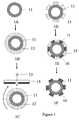
- FIG. 1(A-F)illustrates a method for forming a three-dimensional pattern on an embossing drum or sleeve.
- FIG. 2shows an electroplating mechanism that includes a non-conductive thickness uniformer inserted between a cathode and an anode.
- FIG. 3shows an alternative electroplating mechanism that includes a small-sized anode.
- FIG. 4illustrates a chart of ampere ⁇ hour vs. position in the L-direction.
- FIG. 5Ashows an array of micro-posts on the outer surface of an embossing drum or sleeve.
- FIG. 5Bshows an array of micro-bars on the outer surface of an embossing drum or sleeve.
- FIG. 5Cillustrates a photomask which may be used in a stepwise or continuous exposure process.
- FIG. 6shows stepwise exposure of a photosensitive material.
- FIGS. 7A and 7Billustrate alternative light sources for the exposure process.
- FIG. 8Ashows an embossing drum or embossing sleeve having micro-posts on its outer surface, where the y-axis of the micro-posts has a projection angle of 45° from the longitudinal axis of the drum or sleeve.
- FIG. 8Bshows an embossing drum or embossing sleeve having micro-posts on its outer surface, where the y-axis of the micro-posts has a 0° projection angle from the longitudinal axis of the drum or sleeve.
- FIG. 8Cillustrates angled exposure of a photosensitive material.
- FIG. 9shows a photolithography method using a mask material.
- FIGS. 10A and 10Bshow expandable inserts.
- FIG. 10Cillustrate an embossing assembly of the present invention in a three-dimensional view.
- the methodis illustrated in FIG. 1 .
- the methodproduces embossing drums or sleeves which have a three-dimensional pattern formed on their outer surface.
- embossing drum or embssing sleeverefers to drums or sleeves which have a three-dimensional pattern on their outer surface.
- embssing drum or embssing sleeveis used so as to distinguish it from a plain drum or a plain sleeve, which does not have a three-dimensional pattern on its outer surface.
- embossing drums or embossing sleevesWhen the embossing drums or embossing sleeves are applied to a surface to be embossed, three-dimensional patterns complementary to the three-dimensional patterns on the outer surface of the embossing drums or embossing sleeves are formed on the embossed surface
- the embossing drummay be used directly as an embossing tool (also referred to as an embossing assembly).
- embossing sleeveWhen used for embossing, it is usually mounted on a plain drum to allow rotation of the embossing sleeve.
- the embossing drum or embossing sleeve ( 11 )is usually formed of a conductive material, such as a metal (e.g., aluminum, copper, zinc, nickel, chromium, iron, titanium, cobalt or the like), an alloy derived from any of the aforementioned metals, or stainless steel.
- a metale.g., aluminum, copper, zinc, nickel, chromium, iron, titanium, cobalt or the like
- an alloy derived from any of the aforementioned metalse.g., aluminum, copper, zinc, nickel, chromium, iron, titanium, cobalt or the like
- an alloy derived from any of the aforementioned metalse.g., aluminum, copper, zinc, nickel, chromium, iron, titanium, cobalt or the like
- an alloy derived from any of the aforementioned metalse.g., aluminum, copper, zinc, nickel, chromium, iron, titanium, cobalt or the like
- the embossing drum or embossing sleeve ( 11 )may be formed of a non-conductive material with a conductive coating or a conductive seed layer on its outer surface. Further alternatively, the embossing drum or embossing sleeve ( 11 ) may be formed of a non-conductive material without a conductive material on its outer surface.
- a photosensitive material ( 12 )Before coating a photosensitive material ( 12 ) on the outer surface of a drum or sleeve ( 11 ), as shown in the step of FIG. 1B , precision grinding and polishing may be used to ensure smoothness of the outer surface of the drum or sleeve.
- the photosensitive materialmay be of a positive tone, negative tone or dual tone.
- the photosensitive materialmay also be a chemically amplified photoresist.
- the coatingmay be carried out using dip, spray, drain or ring coating.
- the thickness of the photosensitive materialis preferably greater than the depth or height of the three-dimensional pattern to be formed.
- the photosensitive materialis subjected to exposure as shown in FIG. 1C .
- the photosensitive material ( 12 )can be a dry film photoresist (which is usually commercially available) that is laminated onto the outer surface of the drum or sleeve ( 11 ).
- a suitable light sourcee.g., IR, UV, e-beam or laser
- IR, UV, e-beam or laseris used to expose the photosensitive material ( 12 ) coated on the drum or sleeve ( 11 ).
- a photomask ( 14 )is optionally used to define the three-dimensional pattern to be formed on the photosensitive material. Depending on the pattern, the exposure can be step-by-step, continuous or a combination thereof, the details of which are given below.
- the photosensitive material ( 12 )may be subjected to post-exposure treatment, e.g., baking, before development. Depending on the tone of the photosensitive material, either exposed or un-exposed areas will be removed by using a developer.
- post-exposure treatmente.g., baking
- the drum or sleeve with a patterned photosensitive material ( 15 ) on its outer surfacemay be subjected to baking or blanket exposure before deposition (e.g., electroplating, electroless plating, physical vapor deposition, chemical vapor deposition or sputtering deposition).
- a variety of metals or alloyscan be electroplated and/or electroless plated onto the drum or sleeve.
- the plating material ( 16 )is deposited on the outer surface of the drum or sleeve in areas that are not covered by the patterned photosensitive material.
- the deposit thicknessis preferably less than that of the photosensitive material, as shown in FIG. 1E .
- the thickness variation of the deposit over the whole drum or sleeve areacan be controlled to be less than 1%, by adjusting plating conditions, e.g., the distance between the anode and the cathode (i.e., drum or sleeve) if electroplating is used, the rotation speed of the drum or sleeve and/or circulation of the plating solution.
- plating conditionse.g., the distance between the anode and the cathode (i.e., drum or sleeve) if electroplating is used, the rotation speed of the drum or sleeve and/or circulation of the plating solution.
- the thickness variation of the deposit over the entire surface of the drum or sleevemay be controlled by inserting a non-conductive thickness uniformer ( 20 ) between the cathode (i.e., the drum or sleeve) ( 21 ) and the anode ( 22 ), as shown in FIG. 2 .
- the uniformer ( 20 )may be of a flat or curved layer or of a circular shape (i.e., in the shape of a sleeve), depending on the layout of the cathode and the anode.
- the uniformerhas a narrow opening or openings ( 23 ).
- the uniformermoves in the longitudinal direction of the drum or sleeve back and forth while the drum or sleeve rotates. Since the uniformer is formed of a non-conductive material, e.g., PVC (polyvinyl chloride), only the areas of the drum or sleeve that are directly exposed to the anode almost vertically through the openings ( 23 ) are electroplated. In other words, the outer surface areas of the drum or sleeve that are not covered by the patterned photosensitive material ( 15 in FIG. 1 ) continuously take turns to be electroplated.
- PVCpolyvinyl chloride
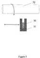
- an anode ( 30 ) of a relatively small size as shown in FIG. 3may be used to homogenize the deposit thickness.
- the anodeis covered with a non-conductive material ( 31 ) except the side facing the cathode (i.e., the drum or sleeve) ( 32 ).
- a non-conductive material31
- the side facing the cathodei.e., the drum or sleeve
- the anodemoves together with the non-conductive material in the longitudinal direction of the drum or sleeve back and forth while the drum or sleeve rotates.
- the anodemay have a flat or curved side facing the cathode.
- FIG. 4shows a monitoring chart the data of which are received from an ampere-hour meter and an anode position gauge or transducer during electroplating.
- the value of the ampere-houris proportional to the deposit thickness.
- the monitoring chartis continuously updated during electroplating; therefore the thickness uniformity over the entire drum or sleeve may be monitored in situ and adjusted, if necessary.
- FIG. 4indicates that the plated deposit in zone 1 and zone 3 is thicker than that of zone 2 .
- the uniformer ( 20 in FIG. 2 ) or the anode ( 30 in FIG. 3 ) used in the two processesmay be adjusted to move faster in zone 1 and zone 3 and/or to move slower in zone 2 to homogenize the deposit thickness over the entire drum or sleeve.
- the platingcan be carried out on a drum or sleeve that is made of a conductive material or a non-conductive material with a conductive coating or a conductive seed layer on its outer surface.
- the three dimensional patternmay be prepared by a method combining photolithography and etching, the details of which are given below.
- the patterned photosensitive material ( 15 )can be stripped by a stripper (e.g., an organic solvent or aqueous solution).
- a strippere.g., an organic solvent or aqueous solution.
- a precision polishingmay be optionally employed to ensure acceptable thickness variation and degree of roughness of the deposit over the entire drum or sleeve.
- FIG. 1Fshows a cross-section view of an embossing drum or embossing sleeve with a three-dimensional pattern formed thereon.
- the plated materialis relatively soft or susceptible to humidity, e.g., copper or zinc
- a relatively wearable or inert layere.g., nickel or chrome
- the deposition of the second layermay be carried out by electroplating, electroless plating, physical vapor deposition, chemical vapor deposition or sputtering deposition, over the entire outer surface of the drum or sleeve.
- the plating step of FIG. 1Emay be replaced by physical vapor deposition, chemical vapor deposition or sputtering deposition.
- the depositionis performed on the entire outer surface of the drum or sleeve. Since the deposit is so thin, the material deposited on top of the photosensitive material may be removed together with the photosensitive material in the stripping step.
- the embossing drum or embossing sleevemay be prepared by a method combining photolithography and etching instead of photolithography and deposition. After coating, exposing and developing (i.e., removal of selective areas of the photosensitive material) of a photosensitive material, an etching step is subsequently performed in areas not covered by the photosensitive material.
- the depth of etchingmay be controlled by the concentration of the etchant used, if a liquid type etchant is used (such as a ferric chloride solution to etch a copper drum or sleeve) or by etching flux intensity, if dry etching (chemical plasma etching, synergetic reactive ion etching or physical ion-beam etching) is used.
- a liquid type etchantsuch as a ferric chloride solution to etch a copper drum or sleeve
- etching flux intensityif dry etching (chemical plasma etching, synergetic reactive ion etching or physical ion-beam etching) is used.
- dry etchingchemical plasma etching, synergetic reactive ion etching or physical ion-beam etching
- the depth of etchingmay also be controlled by temperature and etching time. Alternatively, the depth of etching may be controlled to be uniform by using a selective etch
- a nickel layeris plated on the sleeve or drum first and then a copper layer with a desired thickness is plated on the top of the nickel layer. Since nickel will not be attacked by any of the copper etchants, e.g., ferric chloride, the etching depth can be well controlled. After the etching step, the remaining photosensitive material is removed by using a stripper, and subsequently a relatively wearable or inert layer, e.g., nickel or chrome, may be optionally deposited, as described above, over the entire outer surface of the drum or sleeve.
- a relatively wearable or inert layere.g., nickel or chrome
- a three-dimensional pattern on the embossing drum or embossing sleeve prepared from the process as described above involving an additive (i.e., electroplating, electroless plating, physical vapor deposition, chemical vapor deposition or sputtering deposition) stepwould be structurally complementary to a three-dimensional pattern prepared from the process as described above involving a subtractive (i.e., etching) step.
- additivei.e., electroplating, electroless plating, physical vapor deposition, chemical vapor deposition or sputtering deposition
- FIG. 1Cshows an array of micro-posts on the embossing drum or embossing sleeve.
- a photomask as shown in FIG. 5Cmay be used to stepwise expose the photosensitive material coated on the outer surface of the drum or sleeve. There are a number of ways for stepwise exposure.
- One of the methodsinvolves the use of a pulse type light source.
- the photomask ( 60 )remains stationary throughout the process.
- the exposure of the photosensitive material ( 61 , curvature not shown) coated on the outer surface of the drum or sleeve, through the photomaskoccurs when the drum or sleeve is in the “stop” mode and the pulse type light source is on.
- the areas ( 1 a )-( 1 d ) on the photosensitive materialare exposed corresponding to the openings (a)-(d) of the photomask.
- the drum or sleeveis then rotated to allow exposure of ( 2 a )-( 2 d ).
- the pulse light sourceis off.
- the photosensitive materialis stepwise exposed.
- scanning of the light sourcemay be implemented for exposure while the pulse type light source is on.
- a shuttermay also be used to control the on and off states of the light source.
- the same photomask of FIG. 5Cmay be used for exposure. However, in this case, the exposure is continuous while the embossing drum or embossing sleeve is rotating.
- micro-posts and micro-barsare shown in the figures, it is understood that the three-dimensional pattern on the embossing drum or embossing sleeve may be of any shapes or sizes. A wide variety of sizes may be achieved for the elements (such as the micro-posts) on the three-dimensional pattern, ranging from sub-microns to much larger.
- a collimated light source ( 73 A)e.g., laser
- an opaque patterned thin layer ( 75 )e.g., chrome
- a transparent substrate ( 74 )e.g., glass
- the shape and spot size of the collimated light source ( 73 A)can be controlled by the combination of mirrors and lenses, there will be no need to use a photomask for exposure of the photosensitive material ( 72 ) coated on the drum or sleeve ( 71 ).
- the transparent substrate ( 74 )may be sandwiched between two opaque patterned thin layers ( 75 A and 75 B) to collimate the impinging light as shown in FIG. 7B .
- the photomaskmay also be made of a single opaque layer with suitable openings to allow the light to go through.
- the three-dimensional patternis micro-posts
- the y axis of the micro-postshas a projection angle from the longitudinal axis (L) of the drum or sleeve.
- the projection angle ( ⁇ )is an oblique angle, preferably about 10° to about 80°, more preferably about 30° to about 60° and most preferably about 45°.
- FIG. 8Ashows micro-posts having a projection angle of 45°.
- FIG. 8Bshows micro-posts having a projection angle of 0° (i.e., the y axis of the micro-posts is parallel to the longitudinal axis of the drum or sleeve).
- a continuous spiral line ( 81 )is formed on a photosensitive material coated on the outer surface of a drum or sleeve via exposure of the photosensitive material to a light source ( 80 ).
- the photosensitive materialis preferably of a negative tone.
- the subsequent step of developing the photosensitive materialwill remove the areas which are not covered by the spiral line.
- the area of the spiral linecorresponds to the groove between the micro-posts eventually formed. Therefore, the width of the spiral line ( 81 ) should be substantially equal to the width of the grooves between the micro-posts.
- micro-cavitiesIn contrast to the formation of micro-posts having protruding elements by “angled exposure”, it is also possible to form micro-cavities by using a photosensitive material of a positive tone.
- a photosensitive material of a positive toneWhen a photosensitive material of a positive tone is used, the step of developing the photosensitive material will remove the areas which are covered by the spiral lines. In other words, the areas of the spiral lines correspond to the partition walls between the cavities eventually formed on the embossing drum or embossing sleeve.
- the steps of FIGS. 1E and 1Fmay be modified.
- the thickness of the plating material ( 16 )may exceed the height of the photosensitive material ( 15 ).
- the top area of the plating material beyond the photosensitive materialmay be wider than the bottom area because in the top area there is no photosensitive material to limit the width of the plating material.
- a structure prepared from such a methodis useful for other applications, such as cell wells on a gravure cylinder to transfer printing ink to a substrate.
- the continuous spiral line ( 81 ) in FIG. 8Chas a 45° projection angle from the longitudinal axis (L) of the drum or sleeve.
- the light source ( 80 )steadily moves in the direction of the longitudinal axis (either left to right or right to left) of the drum or sleeve and the drum or sleeve simultaneously rotates (either clockwise or counter clockwise).
- the exposurecan be accomplished by moving the drum or sleeve in the direction of the longitudinal axis of the drum or sleeve and simultaneously rotating the drum or sleeve while the light source ( 80 ) is kept stationary.
- the light sourcemay be rotating around the sleeve or drum while the drum or sleeve moves in the direction of the longitudinal axis.
- the starting point of exposureis shifted one pitch distance away from the previous spiral line ( 81 ) already exposed.
- the spiral lines ( 82 and 82 a ) in an opposite directionare formed by exposure in a manner similar to the process for the exposure of lines 81 and 81 a , except that the light source or the drum or sleeve moves in an opposite direction during exposure.
- the lines 82 and 82 aare perpendicular to the lines 81 and 81 a.
- the spiral lines 81 and 81 amay be exposed by moving the light source in one direction, left to right, at a certain speed and simultaneously rotating the drum or sleeve, counter clockwise, at a certain speed and the spiral lines 82 and 82 a may then be exposed by changing the moving direction of the light source (from “left to right” to “right to left”); but maintaining the same rotation direction of the drum or sleeve (counter clockwise).
- the spiral lines 82 and 82 amay be exposed by changing the rotation direction of the drum or sleeve (from counter clockwise to clockwise); but maintaining the moving direction of the light source (left to right).
- the spiral linesmay be exposed by several overlapping light scans. If the spot size of light source is larger than the width of the grooves, a photomask may be needed to confine the exposure.
- the movement of the photomaskmust be synchronized with the movement of the light source.
- An embossing drum or embossing sleeve having micro-posts prepared by angled exposurehas the advantage that the angle assists the flow of the embossable composition used in the embossing process, thus eliminating trapped air on cross web directions.
- an additional layer of a mask material ( 90 )may be placed over the photosensitive material ( 91 ), as shown in FIG. 9A , by using ring coating, drain coating, spray coating, physical vapor deposition, chemical vapor deposition or sputtering deposition.
- the photosensitive material ( 91 )is coated over the surface ( 92 ) of the drum or sleeve (curvature not shown).
- the mask materialmay also be a photosensitive material that, on the one hand, can be imaged by using a light source with a wavelength different from that needed for the exposure of the photosensitive material ( 91 ), and on the other hand, has a high optical density at the wavelength range used to expose the photosensitive material ( 91 ).
- the patterned mask material ( 90 a )serves as a photomask to expose the photosensitive material ( 91 ) underneath.
- a silver-halide coating and an i-line photoresistmay be used together as the mask material ( 90 ) and the photosensitive material ( 91 ), respectively.
- the silver-halide coatingcan be imaged using a laser diode with a wavelength of 670 nm, and the i-line photoresist can only be imaged using UV light with a wavelength of 365 nm.
- the silver-halide coatingis transferred to a patterned metallic silver layer that is opaque and can be used as a photomask for the exposure of the i-line photoresist underneath.
- the mask materialmay be a laser ablatable material ( 90 in FIG. 9A ) that includes a polymeric matrix having a carbon pigment and an ultraviolet absorbing dye.
- the patterned ablatable material ( 90 a )is used as a photomask for the exposure of the photosensitive material ( 91 ) underneath.
- a plating material ( 93 )is deposited on the outer surface of the drum or sleeve in areas that are not covered by the patterned photosensitive material ( 91 a ).
- a barrier layermay be coated between the photosensitive material ( 91 ) and the mask material ( 90 ).
- the purpose of the barrier layeris to avoid the possible attack on the photosensitive material ( 91 ) by the solvent in the mask material ( 90 ) during the coating process.
- a layer of PVOHpolyvinyl alcohol
- a layer of PVOHpolyvinyl alcohol
- the solvent in the mask material solutionis not miscible with PVOH. In this case, the solvent in the mask material cannot penetrate the barrier layer to attack the photosensitive material.
- the embossing sleeveWhen the embossing sleeve is used for embossing, it is usually mounted on a plain drum to allow rotation of the sleeve. Therefore the embossing sleeve preferably has an inside diameter which is slightly larger than the outside diameter of the plain drum in order to allow the sleeve to be mounted on the drum.
- the 3-dimensional pattern is formed on an embossing sleevehas many advantages over having the pattern directly formed on an embossing drum.
- the sleeveis much lighter than a drum, only about one tenth or less of the weight of a drum; therefore it is much easier to handle.
- Another advantage of using an embossing sleeveis that different sleeves may be fitted to be used on the same plain drum, which effectively reduces the number of drums required, thus saving manufacturing costs.
- the thickness of the embossing sleevepreferably may range from 1 mm to 100 mm, more preferably from 3 mm to 50 mm.
- the sleeveWhen an embossing sleeve is used for embossing, the sleeve must be snugly fitted over the plain drum.
- the tight fittingmay be accomplished by pressure fit involving different materials having different thermal expansion coefficients.
- the tight fittingmay be accomplished by mechanical taper fit.
- FIGS. 10A and 10Billustrate such an expandable insert ( 100 ).
- the insertis a layer of a circular shape which may have one or multiple gaps ( 101 ) as shown in the figures.
- tightening meanssuch as screws
- the diameter of the insertmay be adjusted to ensure tight fitting of the embossing sleeve over the insert and simultaneously the concentricity of the embossing sleeve over the drum.
- the insertis formed of a material, such as a metal (e.g., aluminum, copper, zinc, nickel, iron, titanium, cobalt or the like), an alloy or metal oxide derived from the aforementioned metals or stainless steel. If the insert material is relatively susceptible to humidity or chemical, e.g., copper or iron, a relatively inert layer may be employed to protect it. The deposition of the inert material may be carried out by electroplating, electroless plating, physical vapor deposition, chemical vapor deposition or sputtering deposition, over the entire surface of the insert. Alternatively, the insert may be formed of a plastic material, e.g., PVC (polyvinyl chloride) or ABS (acrylonitrile butadiene styrene).
- PVCpolyvinyl chloride
- ABSacrylonitrile butadiene styrene
- the thickness of the expandable insertpreferably may range from 1 mm to 100 mm, more preferably from 3 mm to 50 mm.
- the expansion of the insertis controlled by the adjustment of screws ( 102 ), preferably with a torque wrench, to ensure proper tightness of the screws.
- screwsWhen the screws are tightened (i.e., screwed down), the insert will expand to cause more contact between the inner surface of the sleeve and the outer surface of the insert, thus tightly holding the sleeve in position.
- the tightness of all of screwsmust be carefully oriented so that the concentricity of the embossing sleeve over the plain drum ( 103 ) may be simultaneously maintained. As explained earlier, the concentricity of the embossing sleeve over the plain drum is critically important to the quality of the embossed microstructures prepared from the embossing assembly.
Landscapes
- Chemical & Material Sciences (AREA)
- Chemical Kinetics & Catalysis (AREA)
- Organic Chemistry (AREA)
- Engineering & Computer Science (AREA)
- Materials Engineering (AREA)
- Metallurgy (AREA)
- General Chemical & Material Sciences (AREA)
- Mechanical Engineering (AREA)
- Electrochemistry (AREA)
- Medicinal Chemistry (AREA)
- Health & Medical Sciences (AREA)
- Polymers & Plastics (AREA)
- Shaping Of Tube Ends By Bending Or Straightening (AREA)
- Exposure And Positioning Against Photoresist Photosensitive Materials (AREA)
- Manufacture Or Reproduction Of Printing Formes (AREA)
- Shaping Metal By Deep-Drawing, Or The Like (AREA)
- Machines For Manufacturing Corrugated Board In Mechanical Paper-Making Processes (AREA)
- Chemically Coating (AREA)
- Electroplating Methods And Accessories (AREA)
- ing And Chemical Polishing (AREA)
Abstract
Description
Claims (21)
Priority Applications (6)
| Application Number | Priority Date | Filing Date | Title |
|---|---|---|---|
| US11/498,529US7767126B2 (en) | 2005-08-22 | 2006-08-02 | Embossing assembly and methods of preparation |
| KR1020087007000AKR101291996B1 (en) | 2005-08-22 | 2006-08-15 | Embossing assembly and methods of preparation |
| CN2006800370695ACN101588916B (en) | 2005-08-22 | 2006-08-15 | Embossed components and methods of making the same |
| PCT/US2006/032251WO2007024643A2 (en) | 2005-08-22 | 2006-08-15 | Embossing assembly and methods of preperation |
| JP2008528003AJP2009508710A (en) | 2005-08-22 | 2006-08-15 | Embossing assembly and manufacturing method |
| EP06789843AEP1943297A2 (en) | 2005-08-22 | 2006-08-15 | Embossing assembly and methods of preparation |
Applications Claiming Priority (4)
| Application Number | Priority Date | Filing Date | Title |
|---|---|---|---|
| US71047705P | 2005-08-22 | 2005-08-22 | |
| US71681705P | 2005-09-13 | 2005-09-13 | |
| US77226106P | 2006-02-10 | 2006-02-10 | |
| US11/498,529US7767126B2 (en) | 2005-08-22 | 2006-08-02 | Embossing assembly and methods of preparation |
Publications (2)
| Publication Number | Publication Date |
|---|---|
| US20070042129A1 US20070042129A1 (en) | 2007-02-22 |
| US7767126B2true US7767126B2 (en) | 2010-08-03 |
Family
ID=37767614
Family Applications (1)
| Application Number | Title | Priority Date | Filing Date |
|---|---|---|---|
| US11/498,529Active2026-10-18US7767126B2 (en) | 2005-08-22 | 2006-08-02 | Embossing assembly and methods of preparation |
Country Status (6)
| Country | Link |
|---|---|
| US (1) | US7767126B2 (en) |
| EP (1) | EP1943297A2 (en) |
| JP (1) | JP2009508710A (en) |
| KR (1) | KR101291996B1 (en) |
| CN (1) | CN101588916B (en) |
| WO (1) | WO2007024643A2 (en) |
Cited By (13)
| Publication number | Priority date | Publication date | Assignee | Title |
|---|---|---|---|---|
| US20130069276A1 (en)* | 2010-06-22 | 2013-03-21 | Boegli-Gravures S.A. | Foil embossing device |
| US20130228468A1 (en)* | 2010-09-30 | 2013-09-05 | Zhuhai Richview Electronics Co., Ltd. | Method for Continuously Producing Flexible Copper Clad Laminates |
| US10401668B2 (en) | 2012-05-30 | 2019-09-03 | E Ink California, Llc | Display device with visually-distinguishable watermark area and non-watermark area |
| WO2020033787A1 (en) | 2018-08-10 | 2020-02-13 | E Ink California, Llc | Driving waveforms for switchable light-collimating layer including bistable electrophoretic fluid |
| WO2020033175A1 (en) | 2018-08-10 | 2020-02-13 | E Ink California, Llc | Switchable light-collimating layer including bistable electrophoretic fluid |
| US10698265B1 (en) | 2017-10-06 | 2020-06-30 | E Ink California, Llc | Quantum dot film |
| US10802373B1 (en) | 2017-06-26 | 2020-10-13 | E Ink Corporation | Reflective microcells for electrophoretic displays and methods of making the same |
| US10921676B2 (en) | 2017-08-30 | 2021-02-16 | E Ink Corporation | Electrophoretic medium |
| US11314098B2 (en) | 2018-08-10 | 2022-04-26 | E Ink California, Llc | Switchable light-collimating layer with reflector |
| US11492717B2 (en) | 2017-11-09 | 2022-11-08 | Lg Energy Solution, Ltd. | Manufacturing apparatus of electrolytic copper foil |
| WO2025147504A1 (en) | 2024-01-05 | 2025-07-10 | E Ink Corporation | An electrophoretic medium comprising particles having a pigment core and a polymeric shell |
| WO2025147410A2 (en) | 2024-01-02 | 2025-07-10 | E Ink Corporation | Electrophoretic media comprising a cationic charge control agent |
| WO2025151355A1 (en) | 2024-01-08 | 2025-07-17 | E Ink Corporation | Electrophoretic device having an adhesive layer comprising conductive filler particles and a polymeric dispersant |
Families Citing this family (18)
| Publication number | Priority date | Publication date | Assignee | Title |
|---|---|---|---|---|
| FR2899502B1 (en)* | 2006-04-06 | 2009-04-10 | Macdermid Printing Solutions E | EMBOSSING DEVICE, SUCH AS A CYLINDER OR SLEEVE |
| US8241479B2 (en)* | 2008-07-10 | 2012-08-14 | Illinois Tool Works Inc. | Imaging of deep structures of reliefs for shallow relief embossing |
| KR101034297B1 (en)* | 2009-08-14 | 2011-05-16 | 주식회사 케이씨씨 | Emboss roll, emboss roll manufacturing method, and decoration sheet manufacturing method using emboss roll |
| JP5544789B2 (en)* | 2009-08-19 | 2014-07-09 | 学校法人東京理科大学 | Endless pattern manufacturing method, resin pattern molded product manufacturing method, endless mold, and optical element |
| US20110195266A1 (en)* | 2010-02-06 | 2011-08-11 | Illinois Tool Works | Seamless sleeve and seamless substrate |
| WO2013002734A1 (en)* | 2011-06-28 | 2013-01-03 | Agency For Science, Technology And Research | Imprinting apparatus and method |
| DE102011108665A1 (en)* | 2011-07-27 | 2013-01-31 | Gallus Druckmaschinen Gmbh | Induction heated cylinder |
| US20140050814A1 (en)* | 2012-08-17 | 2014-02-20 | Gary Yih-Ming Kang | Embossing assembly and methods of preparation |
| JP6121167B2 (en)* | 2013-01-11 | 2017-04-26 | 旭化成株式会社 | Electron beam exposure roll and manufacturing method thereof |
| CN104220647B (en)* | 2013-02-12 | 2017-09-29 | 株式会社新克 | Continuous plating pattern formation roller and its manufacture method |
| US20160059442A1 (en)* | 2014-09-02 | 2016-03-03 | E Ink California, Llc | Embossing tool and methods of preparation |
| JP6382729B2 (en)* | 2015-01-14 | 2018-08-29 | 富士フイルム株式会社 | Method for producing cylindrical pattern film, method for producing pattern roll, and peeling apparatus |
| US10737462B2 (en) | 2016-08-24 | 2020-08-11 | Hyundai Motor Company | Method for coating surface of moving part of vehicle and moving part of vehicle manufactured by the same |
| KR101976924B1 (en)* | 2016-08-24 | 2019-05-13 | 현대자동차주식회사 | Coating method for moving part of vehicle and moving part of vehicle manufactured by the same |
| EP3759551A4 (en)* | 2018-02-26 | 2021-11-24 | Carpe Diem Technologies, Inc. | SYSTEM AND METHOD FOR MANUFACTURING A ROLL-LIKE NANOIMPRINT LITHOGRAPH (RNIL) MASTER |
| EP3575447A1 (en)* | 2018-05-28 | 2019-12-04 | The Swatch Group Research and Development Ltd | Method for producing a metal decoration on a dial and dial obtained according to said method |
| CN108957961A (en)* | 2018-06-26 | 2018-12-07 | 无锡光群雷射科技有限公司 | Holographic laser cylinder version production method |
| ES2992015T3 (en) | 2018-07-25 | 2024-12-05 | Suominen Corp | 3D printed sleeve |
Citations (48)
| Publication number | Priority date | Publication date | Assignee | Title |
|---|---|---|---|---|
| US3239441A (en)* | 1961-06-09 | 1966-03-08 | Marosi Prec Products Co Inc | Method and apparatus for electrolytic production of printed circuits |
| US3637468A (en)* | 1968-04-29 | 1972-01-25 | Dalic Sa | Electrodes for electrolytic processes |
| USRE28068E (en)* | 1972-02-03 | 1974-07-09 | Article decoration apparatus and method | |
| US3900359A (en)* | 1973-02-26 | 1975-08-19 | Dynamics Res Corp | Method and apparatus for television tube shadow mask |
| US3936545A (en)* | 1971-12-03 | 1976-02-03 | Robert Bosch G.M.B.H. | Method of selectively forming oxidized areas |
| US3986939A (en)* | 1975-01-17 | 1976-10-19 | Western Electric Company, Inc. | Method for enhancing the bondability of metallized thin film substrates |
| US4022927A (en)* | 1975-06-30 | 1977-05-10 | International Business Machines Corporation | Methods for forming thick self-supporting masks |
| US4077864A (en)* | 1973-09-10 | 1978-03-07 | General Dynamics | Electroforming anode shields |
| JPS53119228A (en)* | 1977-03-29 | 1978-10-18 | Toppan Printing Co Ltd | Production of perforated plated metal foil |
| JPS6256125A (en)* | 1985-09-06 | 1987-03-11 | Toyo Tire & Rubber Co Ltd | Manufacture of hose formed with inner layer of sintered wearproof material |
| US4741988A (en)* | 1985-05-08 | 1988-05-03 | U.S. Philips Corp. | Patterned polyimide film, a photosensitive polyamide acid derivative and an electrophoretic image-display cell |
| US4923572A (en) | 1988-09-29 | 1990-05-08 | Hallmark Cards, Incorporated | Image transfer tool |
| JPH03192213A (en)* | 1989-12-21 | 1991-08-22 | Fuji Photo Film Co Ltd | Electrode and formation thereof |
| US5156863A (en) | 1982-09-30 | 1992-10-20 | Stimsonite Corporation | Continuous embossing belt |
| US5177476A (en)* | 1989-11-24 | 1993-01-05 | Copytele, Inc. | Methods of fabricating dual anode, flat panel electrophoretic displays |
| US5200253A (en)* | 1989-08-09 | 1993-04-06 | Dai Nippon Insatsu Kabushiki Kaisha | Hologram forming sheet and process for producing the same |
| US5281325A (en)* | 1992-07-02 | 1994-01-25 | Berg N Edward | Uniform electroplating of printed circuit boards |
| US5326455A (en)* | 1990-12-19 | 1994-07-05 | Nikko Gould Foil Co., Ltd. | Method of producing electrolytic copper foil and apparatus for producing same |
| US5327825A (en) | 1993-05-12 | 1994-07-12 | Transfer Print Foils, Inc. | Seamless holographic transfer |
| US5436034A (en)* | 1992-03-25 | 1995-07-25 | Bayer Aktiengesellschaft | Process for improving the adhesiveness of electrolessly deposited metal films |
| US5460922A (en)* | 1993-01-27 | 1995-10-24 | Motorola, Inc. | Method for fabricating electrode patterns |
| US5483890A (en)* | 1995-03-15 | 1996-01-16 | Gencorp Inc. | Direct applied embossing casting methods |
| US5744013A (en)* | 1996-12-12 | 1998-04-28 | Mitsubishi Semiconductor America, Inc. | Anode basket for controlling plating thickness distribution |
| US5759378A (en)* | 1995-02-10 | 1998-06-02 | Macdermid, Incorporated | Process for preparing a non-conductive substrate for electroplating |
| US5776327A (en)* | 1996-10-16 | 1998-07-07 | Mitsubishi Semiconuctor Americe, Inc. | Method and apparatus using an anode basket for electroplating a workpiece |
| US5834037A (en)* | 1995-12-25 | 1998-11-10 | Wu; Sze Tsang | Apparatus for making insignias with raised designs |
| US5881444A (en) | 1997-12-12 | 1999-03-16 | Aluminum Company Of America | Techniques for transferring holograms into metal surfaces |
| US6027631A (en)* | 1997-11-13 | 2000-02-22 | Novellus Systems, Inc. | Electroplating system with shields for varying thickness profile of deposited layer |
| US6080606A (en)* | 1996-03-26 | 2000-06-27 | The Trustees Of Princeton University | Electrophotographic patterning of thin film circuits |
| US6117300A (en)* | 1996-05-01 | 2000-09-12 | Honeywell International Inc. | Method for forming conductive traces and printed circuits made thereby |
| US6132583A (en)* | 1997-05-16 | 2000-10-17 | Technic, Inc. | Shielding method and apparatus for use in electroplating process |
| US6179983B1 (en)* | 1997-11-13 | 2001-01-30 | Novellus Systems, Inc. | Method and apparatus for treating surface including virtual anode |
| US6280581B1 (en)* | 1998-12-29 | 2001-08-28 | David Cheng | Method and apparatus for electroplating films on semiconductor wafers |
| US6402923B1 (en)* | 2000-03-27 | 2002-06-11 | Novellus Systems Inc | Method and apparatus for uniform electroplating of integrated circuits using a variable field shaping element |
| US20020125140A1 (en)* | 1998-01-22 | 2002-09-12 | Uzoh Cyprian Emeka | Apparatus and methods to control the uniformity of electroplated workpiece |
| US20030008489A1 (en)* | 2001-05-04 | 2003-01-09 | Tessera, Inc. | Method of making bondable leads using positive photoresist and structures made therefrom |
| US6770225B2 (en)* | 1994-09-28 | 2004-08-03 | Reflexite Corporation | Textured retroreflective prism structures and molds for forming same |
| US20040245669A1 (en)* | 2001-09-28 | 2004-12-09 | Taiji Nishi | Method of producing resin molded product |
| WO2005002305A2 (en)* | 2003-06-06 | 2005-01-06 | Sipix Imaging, Inc. | In mold manufacture of an object with embedded display panel |
| US20050023145A1 (en)* | 2003-05-07 | 2005-02-03 | Microfabrica Inc. | Methods and apparatus for forming multi-layer structures using adhered masks |
| US20050121328A1 (en)* | 2002-01-31 | 2005-06-09 | Mitsuhiko Shirakashi | Electrolytic processing apparatus and method |
| US20050239935A1 (en)* | 2004-04-26 | 2005-10-27 | Kang Gary Y | Roll-to-roll embossing tools and processes |
| US6974530B2 (en)* | 2002-06-28 | 2005-12-13 | Advanced Micro Devices, Inc. | Method and system for controlling ion distribution during plating of a metal on a workpiece surface |
| US20060086620A1 (en)* | 2004-10-21 | 2006-04-27 | Chase Lee A | Textured decorative plating on plastic components |
| US20060142853A1 (en)* | 2003-04-08 | 2006-06-29 | Xingwu Wang | Coated substrate assembly |
| US7156945B2 (en) | 2002-04-24 | 2007-01-02 | Sipix Imaging, Inc. | Process for forming a patterned thin film structure for in-mold decoration |
| US20070175762A1 (en)* | 2006-01-11 | 2007-08-02 | Kang Gary Y | Thickness distribution control for electroplating |
| US20070181430A1 (en)* | 1997-04-04 | 2007-08-09 | Cohen Adam L | Method For Electrochemical Fabrication |
Family Cites Families (7)
| Publication number | Priority date | Publication date | Assignee | Title |
|---|---|---|---|---|
| US5266257A (en)* | 1992-05-29 | 1993-11-30 | Gencorp Inc. | Method of making embossing rolls having indicia |
| EP0734827A1 (en)* | 1995-03-28 | 1996-10-02 | Saueressig Gmbh & Co. | Embossing tools for treating materials with a tacky surface during the forming process |
| TWI268813B (en)* | 2002-04-24 | 2006-12-21 | Sipix Imaging Inc | Process for forming a patterned thin film conductive structure on a substrate |
| US6846172B2 (en)* | 2002-06-07 | 2005-01-25 | The Procter & Gamble Company | Embossing apparatus |
| EP1437213A1 (en)* | 2002-12-23 | 2004-07-14 | Boegli-Gravures S.A. | Device for satin-finishing and embossing a flat material |
| JP4464123B2 (en)* | 2003-12-18 | 2010-05-19 | 日清紡ホールディングス株式会社 | Embossing method |
| DE202004011022U1 (en)* | 2004-07-14 | 2004-09-23 | Sca Hygiene Products Gmbh | Embossing roller, especially for multi-layer toilet tissue, has an embossing sleeve fitted over a carrier roller, with a positive fit lock between them in a secure mounting |
- 2006
- 2006-08-02USUS11/498,529patent/US7767126B2/enactiveActive
- 2006-08-15KRKR1020087007000Apatent/KR101291996B1/enactiveActive
- 2006-08-15WOPCT/US2006/032251patent/WO2007024643A2/enactiveApplication Filing
- 2006-08-15CNCN2006800370695Apatent/CN101588916B/enactiveActive
- 2006-08-15JPJP2008528003Apatent/JP2009508710A/enactivePending
- 2006-08-15EPEP06789843Apatent/EP1943297A2/ennot_activeWithdrawn
Patent Citations (49)
| Publication number | Priority date | Publication date | Assignee | Title |
|---|---|---|---|---|
| US3239441A (en)* | 1961-06-09 | 1966-03-08 | Marosi Prec Products Co Inc | Method and apparatus for electrolytic production of printed circuits |
| US3637468A (en)* | 1968-04-29 | 1972-01-25 | Dalic Sa | Electrodes for electrolytic processes |
| US3936545A (en)* | 1971-12-03 | 1976-02-03 | Robert Bosch G.M.B.H. | Method of selectively forming oxidized areas |
| USRE28068E (en)* | 1972-02-03 | 1974-07-09 | Article decoration apparatus and method | |
| US3900359A (en)* | 1973-02-26 | 1975-08-19 | Dynamics Res Corp | Method and apparatus for television tube shadow mask |
| US4077864A (en)* | 1973-09-10 | 1978-03-07 | General Dynamics | Electroforming anode shields |
| US3986939A (en)* | 1975-01-17 | 1976-10-19 | Western Electric Company, Inc. | Method for enhancing the bondability of metallized thin film substrates |
| US4022927A (en)* | 1975-06-30 | 1977-05-10 | International Business Machines Corporation | Methods for forming thick self-supporting masks |
| JPS53119228A (en)* | 1977-03-29 | 1978-10-18 | Toppan Printing Co Ltd | Production of perforated plated metal foil |
| US5156863A (en) | 1982-09-30 | 1992-10-20 | Stimsonite Corporation | Continuous embossing belt |
| US4741988A (en)* | 1985-05-08 | 1988-05-03 | U.S. Philips Corp. | Patterned polyimide film, a photosensitive polyamide acid derivative and an electrophoretic image-display cell |
| JPS6256125A (en)* | 1985-09-06 | 1987-03-11 | Toyo Tire & Rubber Co Ltd | Manufacture of hose formed with inner layer of sintered wearproof material |
| US4923572A (en) | 1988-09-29 | 1990-05-08 | Hallmark Cards, Incorporated | Image transfer tool |
| US5200253A (en)* | 1989-08-09 | 1993-04-06 | Dai Nippon Insatsu Kabushiki Kaisha | Hologram forming sheet and process for producing the same |
| US5177476A (en)* | 1989-11-24 | 1993-01-05 | Copytele, Inc. | Methods of fabricating dual anode, flat panel electrophoretic displays |
| JPH03192213A (en)* | 1989-12-21 | 1991-08-22 | Fuji Photo Film Co Ltd | Electrode and formation thereof |
| US5326455A (en)* | 1990-12-19 | 1994-07-05 | Nikko Gould Foil Co., Ltd. | Method of producing electrolytic copper foil and apparatus for producing same |
| US5436034A (en)* | 1992-03-25 | 1995-07-25 | Bayer Aktiengesellschaft | Process for improving the adhesiveness of electrolessly deposited metal films |
| US5281325A (en)* | 1992-07-02 | 1994-01-25 | Berg N Edward | Uniform electroplating of printed circuit boards |
| US5460922A (en)* | 1993-01-27 | 1995-10-24 | Motorola, Inc. | Method for fabricating electrode patterns |
| US5327825A (en) | 1993-05-12 | 1994-07-12 | Transfer Print Foils, Inc. | Seamless holographic transfer |
| US6770225B2 (en)* | 1994-09-28 | 2004-08-03 | Reflexite Corporation | Textured retroreflective prism structures and molds for forming same |
| US5759378A (en)* | 1995-02-10 | 1998-06-02 | Macdermid, Incorporated | Process for preparing a non-conductive substrate for electroplating |
| US5483890A (en)* | 1995-03-15 | 1996-01-16 | Gencorp Inc. | Direct applied embossing casting methods |
| US5834037A (en)* | 1995-12-25 | 1998-11-10 | Wu; Sze Tsang | Apparatus for making insignias with raised designs |
| US6080606A (en)* | 1996-03-26 | 2000-06-27 | The Trustees Of Princeton University | Electrophotographic patterning of thin film circuits |
| US6117300A (en)* | 1996-05-01 | 2000-09-12 | Honeywell International Inc. | Method for forming conductive traces and printed circuits made thereby |
| US5776327A (en)* | 1996-10-16 | 1998-07-07 | Mitsubishi Semiconuctor Americe, Inc. | Method and apparatus using an anode basket for electroplating a workpiece |
| US5744013A (en)* | 1996-12-12 | 1998-04-28 | Mitsubishi Semiconductor America, Inc. | Anode basket for controlling plating thickness distribution |
| US20070181430A1 (en)* | 1997-04-04 | 2007-08-09 | Cohen Adam L | Method For Electrochemical Fabrication |
| US6132583A (en)* | 1997-05-16 | 2000-10-17 | Technic, Inc. | Shielding method and apparatus for use in electroplating process |
| US6179983B1 (en)* | 1997-11-13 | 2001-01-30 | Novellus Systems, Inc. | Method and apparatus for treating surface including virtual anode |
| US6027631A (en)* | 1997-11-13 | 2000-02-22 | Novellus Systems, Inc. | Electroplating system with shields for varying thickness profile of deposited layer |
| US6006415A (en) | 1997-12-12 | 1999-12-28 | Aluminum Company Of America | Techniques for transferring holograms into metal surfaces |
| US5881444A (en) | 1997-12-12 | 1999-03-16 | Aluminum Company Of America | Techniques for transferring holograms into metal surfaces |
| US20020125140A1 (en)* | 1998-01-22 | 2002-09-12 | Uzoh Cyprian Emeka | Apparatus and methods to control the uniformity of electroplated workpiece |
| US6280581B1 (en)* | 1998-12-29 | 2001-08-28 | David Cheng | Method and apparatus for electroplating films on semiconductor wafers |
| US6402923B1 (en)* | 2000-03-27 | 2002-06-11 | Novellus Systems Inc | Method and apparatus for uniform electroplating of integrated circuits using a variable field shaping element |
| US20030008489A1 (en)* | 2001-05-04 | 2003-01-09 | Tessera, Inc. | Method of making bondable leads using positive photoresist and structures made therefrom |
| US20040245669A1 (en)* | 2001-09-28 | 2004-12-09 | Taiji Nishi | Method of producing resin molded product |
| US20050121328A1 (en)* | 2002-01-31 | 2005-06-09 | Mitsuhiko Shirakashi | Electrolytic processing apparatus and method |
| US7156945B2 (en) | 2002-04-24 | 2007-01-02 | Sipix Imaging, Inc. | Process for forming a patterned thin film structure for in-mold decoration |
| US6974530B2 (en)* | 2002-06-28 | 2005-12-13 | Advanced Micro Devices, Inc. | Method and system for controlling ion distribution during plating of a metal on a workpiece surface |
| US20060142853A1 (en)* | 2003-04-08 | 2006-06-29 | Xingwu Wang | Coated substrate assembly |
| US20050023145A1 (en)* | 2003-05-07 | 2005-02-03 | Microfabrica Inc. | Methods and apparatus for forming multi-layer structures using adhered masks |
| WO2005002305A2 (en)* | 2003-06-06 | 2005-01-06 | Sipix Imaging, Inc. | In mold manufacture of an object with embedded display panel |
| US20050239935A1 (en)* | 2004-04-26 | 2005-10-27 | Kang Gary Y | Roll-to-roll embossing tools and processes |
| US20060086620A1 (en)* | 2004-10-21 | 2006-04-27 | Chase Lee A | Textured decorative plating on plastic components |
| US20070175762A1 (en)* | 2006-01-11 | 2007-08-02 | Kang Gary Y | Thickness distribution control for electroplating |
Non-Patent Citations (34)
| Title |
|---|
| Allen, K. (Oct. 2003). Electrophoretics Fulfilled. Emerging Displays Review: Emerging Display Technologies, Monthly Report-Oct. 2003, 9-14. |
| Bardsley, J.N. & Pinnel, M.R. (Nov. 2004) Microcup(TM) Electrophoretic Displays. USDC Flexible Display Report, 3.1.2. pp. 3-12-3-16. |
| Bardsley, J.N. & Pinnel, M.R. (Nov. 2004) Microcup™ Electrophoretic Displays. USDC Flexible Display Report, 3.1.2. pp. 3-12-3-16. |
| Chaug, Y.S., Haubrich, J.E., Sereda, M. and Liang, R.C. (Apr. 2004). Roll-to-Roll Processes for the Manufacturing of Patterned Conductive Electrodes on Flexible Substrates. Mat. Res. Soc. Symp. Proc., vol. 814, I9.6.1. |
| Chen, S.M. (Jul. 2003) The Applications for the Revolutionary Electronic Paper Technology. OPTO News & Letters, 102, 37-41. (in Chinese, English abstract attached, full translation available upon request). |
| Chen, S.M. (May 2003) The New Applications and the Dynamics of Companies. TRI. 1-10. (In Chinese, English abstract attached, full translation availabe upon request). |
| Chung, J., Hou, J., Wang, W., Chu, L.Y., Yao, W., & Liang, R.C. (Dec. 2003). Microcup(R) Electrophoretic Displays, Grayscale and Color Rendition. IDW, AMD2/EP1-2, 243-246. |
| Ho, C.,& Liang, R.C. (Dec. 2003). Microcup (R) Electronic Paper by Roll-to-Roll Manufacturing Processes. Presentation conducted at FEG, Nei-Li, Taiwan. |
| Ho, Candice. (Feb. 1, 2005) Microcupt® Electronic Paper Device and Applicaiton. Presentation conducted at USDC 4th Annual Flexible Display Conference 2005. |
| Hou, J., Chen, Y., Li, Y., Weng, X., Li, H. And Pereira, C. (May 2004). Reliability and Performance of Flexible Electrophoretic Displays by Roll-to-Roll Manufacturing Processes. SID Digest, 32.3, 1066-1069. |
| International Search Report for PCT/US06/32251, mailed Apr. 4, 2008. |
| Lee, H., & Liang, R.C. (Jun. 2003) SiPix Microcup(R) Electronic Paper-An Introduction. Advanced Display, Issue 37, 4-9 (in Chinese, English abstract attached, full translation available upon request). |
| Liang, R.C. (Apr. 2004). Microcup Electronic Paper by Roll-to-Roll Manufacturing Process. Presentation at the Flexible Displays & Electronics 2004 of Intertech, San Fransisco, California, USA. |
| Liang, R.C. (Feb. 2003) Microcup(R) Electrophoretic and Liquid Crystal Displays by Roll-to-Roll Manufacturing Processes. Presentation conducted at the Flexible Microelectronics & Displays Conference of U.S. Display Consortium, Phoenix, Arizona, USA. |
| Liang, R.C. (Oct. 2004) Flexible and Roll-able Display/Electronic Paper-A Technology Overview. Paper presented at the METS 2004 Conference in Taipie, Taiwan. |
| Liang, R.C., & Tseng, S. (Feb. 2003). Microcup(R) LCD, An New Type of Dispersed LCD by A Roll-to-Roll Manufacturing Process. Paper presented at the IDMC, Taipei, Taiwan. |
| Liang, R.C., (Feb. 2005) Flexible and Roll-able Displays/Electronic Paper-A Brief Technology Overview. Flexible Display Forum, 2005, Taiwan. |
| Liang, R.C., Hou, J., & Zang, H.M. (Dec. 2002) Microcup Electrophoretic Displays by Roll-to-Roll Manufacturing Processes. IDW, EP2-2, 1337-1340. |
| Liang, R.C., Hou, J., Chung, J., Wang, X., Pereira, C., & Chen, Y. (2003). Microcup(R) Active and Passive Matrix Electrophoretic Displays by A Roll-to-Roll Manufacturing Processes. SID Digest, 20.1. |
| Liang, R.C., Hou, J., Zang, H.M., & Chung, J. (Feb. 2003). Passive Matrix Microcup(R) Electrophoretic Displays. Paper presented at the IDMC, Taipei, Taiwan. |
| Liang, R.C., Hou, J., Zang, H.M., Chung, J., & Tseng, S. (2003). Microcup(R) displays : Electronic Paper by Roll-to-Roll Manufacturing Processes. Journal of the SID, 11(4), 621-628. |
| Liang, R.C., Zang, H.M., Wang, X., Chung, J. & Lee, H., (Jun./Jul. 2004) << Format Flexible Microcup (R) Electronic Paper by Roll-to-Roll Manufacturing Process >>, Presentation conducted at the 14th FPD Manufacturing Technology Expo & Conference. |
| Liang, R.C., Zang, H.M., Wang, X., Chung, J. & Lee, H., (Jun./Jul. 2004) >, Presentation conducted at the 14th FPD Manufacturing Technology Expo & Conference. |
| Nikkei Microdevices. (Dec. 2002) Newly-Developed Color Electronic Paper Promises-Unbeatable Production Efficiency. Nikkei Microdevices, 3. (in Japanese, with English translation). |
| Wang, X., Kiluk, S., Chang, C., & Liang, R.C. (Feb. 2004). Mirocup (R) Electronic Paper and the Converting Processes. ASID, 10.1.2-26, 396-399, Nanjing, China. |
| Wang, X., Kiluk, S., Chang, C., & Liang, R.C., (Jun. 2004) Microcup® Electronic Paper and the Converting Processes. Advanced Display, Issue 43, 48-51. |
| Wang, X., Li, P., Sodhi, D., Xu, T. and Bruner, S. et al., (Feb. 2006) Inkjet Fabrication of Multi-Color Microcup® Electrophorectic Display. the Flexible Microelectronics & Displays Conference of U.S. Display Consortium. |
| Wang, X., Zang, HM., and Li, P. (Jun. 2006) Roll-to-Roll Manufacturing Process for Full Color Electrophoretic film. SID Digest, pp. 1587-1589. |
| Zang, H.M, Hwang, J.J., Gu, H., Hou, J., Weng, X., Chen, Y., et al. (Jan. 2004). Threshold and Grayscale Stability of Microcup (R) Electronic Paper. Proceeding of SPIE-IS&T Electronic Imaging, SPIE vol. 5289, 102-108. |
| Zang, H.M. (Feb. 2004). Microcup Electronic Paper. Presentation conducted at the Displays & Microelectronics Conference of U.S. Display Consortium, Phoenix, Arizona, USA. |
| Zang, H.M. (Oct. 2003). Microcup (R) Electronic Paper by Roll-to-Roll Manufacturing Processes. Presentation conducted at the Advisory Board Meeting, Bowling Green State University, Ohio, USA. |
| Zang, H.M., & Liang, R.C. (2003) Microcup Electronic Paper by Roll-to-Roll Manufacturing Processes. The Spectrum, 16(2), 16-21. |
| Zang, H.M.Hou, Jack, (Feb. 2005) Flexible Microcup® EPD by RTR Process. Presentation conducted at 2nd Annual Paper-Like Displays Conference, Feb. 9-11, 2005, St. Pete Beach, Florida. |
| Zang, HM., Wang, W., Sun, C., Gu, H., and Chen, Y. (May 2006) Monochrome and Area Color Microcup® EPDs by Roll-to-Roll Manufacturing Processes. ICIS ' 06 International Congress of Imaging Science Final Program and Proceedings, pp. 362-365. |
Cited By (24)
| Publication number | Priority date | Publication date | Assignee | Title |
|---|---|---|---|---|
| US8932044B2 (en)* | 2010-06-22 | 2015-01-13 | Boegli-Gravures S.A. | Foil embossing device |
| US20130069276A1 (en)* | 2010-06-22 | 2013-03-21 | Boegli-Gravures S.A. | Foil embossing device |
| US9587318B2 (en)* | 2010-09-30 | 2017-03-07 | Richview Electronics Co., Ltd. | Method for continuously producing flexible copper clad laminates |
| US20130228468A1 (en)* | 2010-09-30 | 2013-09-05 | Zhuhai Richview Electronics Co., Ltd. | Method for Continuously Producing Flexible Copper Clad Laminates |
| US10401668B2 (en) | 2012-05-30 | 2019-09-03 | E Ink California, Llc | Display device with visually-distinguishable watermark area and non-watermark area |
| US10831052B2 (en) | 2012-05-30 | 2020-11-10 | E Ink California, Llc | Display device with visually-distinguishable watermark area and non-watermark area |
| US10802373B1 (en) | 2017-06-26 | 2020-10-13 | E Ink Corporation | Reflective microcells for electrophoretic displays and methods of making the same |
| US11774827B2 (en) | 2017-06-26 | 2023-10-03 | E Ink Corporation | Reflective microcells for electrophoretic displays and methods of making the same |
| US11372306B2 (en) | 2017-06-26 | 2022-06-28 | E Ink Corporation | Reflective microcells for electrophoretic displays and methods of making the same |
| US11977310B2 (en) | 2017-08-30 | 2024-05-07 | E Ink Corporation | Electrophoretic medium |
| US10921676B2 (en) | 2017-08-30 | 2021-02-16 | E Ink Corporation | Electrophoretic medium |
| US11493805B2 (en) | 2017-10-06 | 2022-11-08 | E Ink California, Llc | Quantum dot film with sealed microcells |
| US10698265B1 (en) | 2017-10-06 | 2020-06-30 | E Ink California, Llc | Quantum dot film |
| US11492717B2 (en) | 2017-11-09 | 2022-11-08 | Lg Energy Solution, Ltd. | Manufacturing apparatus of electrolytic copper foil |
| WO2020033175A1 (en) | 2018-08-10 | 2020-02-13 | E Ink California, Llc | Switchable light-collimating layer including bistable electrophoretic fluid |
| US11435606B2 (en) | 2018-08-10 | 2022-09-06 | E Ink California, Llc | Driving waveforms for switchable light-collimating layer including bistable electrophoretic fluid |
| US11397366B2 (en) | 2018-08-10 | 2022-07-26 | E Ink California, Llc | Switchable light-collimating layer including bistable electrophoretic fluid |
| US11656526B2 (en) | 2018-08-10 | 2023-05-23 | E Ink California, Llc | Switchable light-collimating layer including bistable electrophoretic fluid |
| US11719953B2 (en) | 2018-08-10 | 2023-08-08 | E Ink California, Llc | Switchable light-collimating layer with reflector |
| US11314098B2 (en) | 2018-08-10 | 2022-04-26 | E Ink California, Llc | Switchable light-collimating layer with reflector |
| WO2020033787A1 (en) | 2018-08-10 | 2020-02-13 | E Ink California, Llc | Driving waveforms for switchable light-collimating layer including bistable electrophoretic fluid |
| WO2025147410A2 (en) | 2024-01-02 | 2025-07-10 | E Ink Corporation | Electrophoretic media comprising a cationic charge control agent |
| WO2025147504A1 (en) | 2024-01-05 | 2025-07-10 | E Ink Corporation | An electrophoretic medium comprising particles having a pigment core and a polymeric shell |
| WO2025151355A1 (en) | 2024-01-08 | 2025-07-17 | E Ink Corporation | Electrophoretic device having an adhesive layer comprising conductive filler particles and a polymeric dispersant |
Also Published As
| Publication number | Publication date |
|---|---|
| JP2009508710A (en) | 2009-03-05 |
| EP1943297A2 (en) | 2008-07-16 |
| WO2007024643A2 (en) | 2007-03-01 |
| CN101588916A (en) | 2009-11-25 |
| KR101291996B1 (en) | 2013-08-09 |
| KR20080038242A (en) | 2008-05-02 |
| CN101588916B (en) | 2012-07-04 |
| US20070042129A1 (en) | 2007-02-22 |
| WO2007024643A3 (en) | 2009-05-14 |
Similar Documents
| Publication | Publication Date | Title |
|---|---|---|
| US7767126B2 (en) | Embossing assembly and methods of preparation | |
| EP1905065B1 (en) | Roll-to-roll patterning | |
| US8070970B2 (en) | UV-LIGA process for fabricating a multilayer metal structure having adjacent layers that are not entirely superposed, and the structure obtained | |
| CN101517130B (en) | Method for manufacturing electroformed mold, electroformed mold, and method for manufacturing electroformed parts | |
| TWI518027B (en) | Large area nanopattering method and apparatus | |
| US8840795B2 (en) | Method for manufacturing a master mold which is used to form a micropatterned film applied to an exterior of a household appliance and manufacturing apparatus and method of the film using the master mold | |
| EP1327705A1 (en) | Method for producing metal mask and metal mask | |
| TWI756888B (en) | Method for manufacturing a horological component | |
| US20020100691A1 (en) | 3-dimensional imprint tool | |
| TWI447781B (en) | A method of making a microstructure embossing die | |
| US20040031404A1 (en) | Seamless embossing shim | |
| TW202206947A (en) | Transfer roller, manufacturing method of transfer roller, optical film, and manufacturing method of optical film | |
| CN102758226B (en) | Accurate electroplating machining method for long-grating roller stamping mould for machine tool | |
| US5512161A (en) | Process for galvanically forming structured plate-shaped bodies | |
| JP2021096249A (en) | Method of manufacturing timepiece component and component produced using the same | |
| CN107206825B (en) | Gravure cylinder, method for producing the same, and method for producing printed matter | |
| WO2003040781A1 (en) | Processes using gray scale exposure processes to make microoptical elements and corresponding molds | |
| JP2002105621A (en) | Metal plate, its manufacturing method and aligner | |
| JP2005508269A5 (en) | ||
| TWI762059B (en) | Method for manufacturing a horological component and component produced according to said method | |
| TWI300019B (en) | Embossing assembly and methods of preparation | |
| US20110132768A1 (en) | Method for forming imprinting roller | |
| MX2008002548A (en) | Embossing assembly and methods of preperation | |
| JP2004255883A (en) | Preparation of mask for manufacturing printing plate | |
| TWI233423B (en) | Method of fabricating a stamper with microstructure patterns |
Legal Events
| Date | Code | Title | Description |
|---|---|---|---|
| AS | Assignment | Owner name:SIPIX IMAGING, INC.,CALIFORNIA Free format text:ASSIGNMENT OF ASSIGNORS INTEREST;ASSIGNORS:KANG, GARY YIH-MING;LIU, JOHN HANAN;CHAUG, YI-SHUNG;SIGNING DATES FROM 20060831 TO 20060907;REEL/FRAME:024559/0001 Owner name:SIPIX IMAGING, INC., CALIFORNIA Free format text:ASSIGNMENT OF ASSIGNORS INTEREST;ASSIGNORS:KANG, GARY YIH-MING;LIU, JOHN HANAN;CHAUG, YI-SHUNG;SIGNING DATES FROM 20060831 TO 20060907;REEL/FRAME:024559/0001 | |
| STCF | Information on status: patent grant | Free format text:PATENTED CASE | |
| FPAY | Fee payment | Year of fee payment:4 | |
| AS | Assignment | Owner name:E INK CALIFORNIA, LLC, CALIFORNIA Free format text:CHANGE OF NAME;ASSIGNOR:SIPIX IMAGING, INC.;REEL/FRAME:033280/0408 Effective date:20140701 | |
| MAFP | Maintenance fee payment | Free format text:PAYMENT OF MAINTENANCE FEE, 8TH YEAR, LARGE ENTITY (ORIGINAL EVENT CODE: M1552) Year of fee payment:8 | |
| MAFP | Maintenance fee payment | Free format text:PAYMENT OF MAINTENANCE FEE, 12TH YEAR, LARGE ENTITY (ORIGINAL EVENT CODE: M1553); ENTITY STATUS OF PATENT OWNER: LARGE ENTITY Year of fee payment:12 | |
| AS | Assignment | Owner name:E INK CORPORATION, MASSACHUSETTS Free format text:ASSIGNMENT OF ASSIGNORS INTEREST;ASSIGNOR:E INK CALIFORNIA, LLC;REEL/FRAME:065154/0965 Effective date:20230925 |