US7765426B2 - Emerging bad block detection - Google Patents
Emerging bad block detectionDownload PDFInfo
- Publication number
- US7765426B2 US7765426B2US11/759,585US75958507AUS7765426B2US 7765426 B2US7765426 B2US 7765426B2US 75958507 AUS75958507 AUS 75958507AUS 7765426 B2US7765426 B2US 7765426B2
- Authority
- US
- United States
- Prior art keywords
- block
- read
- page
- error
- memory device
- Prior art date
- Legal status (The legal status is an assumption and is not a legal conclusion. Google has not performed a legal analysis and makes no representation as to the accuracy of the status listed.)
- Active, expires
Links
Images


Classifications
- G—PHYSICS
- G06—COMPUTING OR CALCULATING; COUNTING
- G06F—ELECTRIC DIGITAL DATA PROCESSING
- G06F11/00—Error detection; Error correction; Monitoring
- G06F11/07—Responding to the occurrence of a fault, e.g. fault tolerance
- G06F11/16—Error detection or correction of the data by redundancy in hardware
- G06F11/20—Error detection or correction of the data by redundancy in hardware using active fault-masking, e.g. by switching out faulty elements or by switching in spare elements
- G06F11/2017—Error detection or correction of the data by redundancy in hardware using active fault-masking, e.g. by switching out faulty elements or by switching in spare elements where memory access, memory control or I/O control functionality is redundant
- G—PHYSICS
- G06—COMPUTING OR CALCULATING; COUNTING
- G06F—ELECTRIC DIGITAL DATA PROCESSING
- G06F11/00—Error detection; Error correction; Monitoring
- G06F11/07—Responding to the occurrence of a fault, e.g. fault tolerance
- G06F11/08—Error detection or correction by redundancy in data representation, e.g. by using checking codes
- G06F11/10—Adding special bits or symbols to the coded information, e.g. parity check, casting out 9's or 11's
- G06F11/1008—Adding special bits or symbols to the coded information, e.g. parity check, casting out 9's or 11's in individual solid state devices
- G06F11/1068—Adding special bits or symbols to the coded information, e.g. parity check, casting out 9's or 11's in individual solid state devices in sector programmable memories, e.g. flash disk
- G—PHYSICS
- G06—COMPUTING OR CALCULATING; COUNTING
- G06F—ELECTRIC DIGITAL DATA PROCESSING
- G06F11/00—Error detection; Error correction; Monitoring
- G06F11/07—Responding to the occurrence of a fault, e.g. fault tolerance
- G06F11/0703—Error or fault processing not based on redundancy, i.e. by taking additional measures to deal with the error or fault not making use of redundancy in operation, in hardware, or in data representation
- G06F11/0706—Error or fault processing not based on redundancy, i.e. by taking additional measures to deal with the error or fault not making use of redundancy in operation, in hardware, or in data representation the processing taking place on a specific hardware platform or in a specific software environment
- G06F11/073—Error or fault processing not based on redundancy, i.e. by taking additional measures to deal with the error or fault not making use of redundancy in operation, in hardware, or in data representation the processing taking place on a specific hardware platform or in a specific software environment in a memory management context, e.g. virtual memory or cache management
- G—PHYSICS
- G11—INFORMATION STORAGE
- G11C—STATIC STORES
- G11C16/00—Erasable programmable read-only memories
- G11C16/02—Erasable programmable read-only memories electrically programmable
- G11C16/06—Auxiliary circuits, e.g. for writing into memory
- G11C16/34—Determination of programming status, e.g. threshold voltage, overprogramming or underprogramming, retention
- G11C16/349—Arrangements for evaluating degradation, retention or wearout, e.g. by counting erase cycles
- G—PHYSICS
- G06—COMPUTING OR CALCULATING; COUNTING
- G06F—ELECTRIC DIGITAL DATA PROCESSING
- G06F11/00—Error detection; Error correction; Monitoring
- G06F11/07—Responding to the occurrence of a fault, e.g. fault tolerance
- G06F11/0703—Error or fault processing not based on redundancy, i.e. by taking additional measures to deal with the error or fault not making use of redundancy in operation, in hardware, or in data representation
- G06F11/0751—Error or fault detection not based on redundancy
- G06F11/0754—Error or fault detection not based on redundancy by exceeding limits
- G06F11/076—Error or fault detection not based on redundancy by exceeding limits by exceeding a count or rate limit, e.g. word- or bit count limit
- G—PHYSICS
- G06—COMPUTING OR CALCULATING; COUNTING
- G06F—ELECTRIC DIGITAL DATA PROCESSING
- G06F2201/00—Indexing scheme relating to error detection, to error correction, and to monitoring
- G06F2201/85—Active fault masking without idle spares
Definitions
- Embodiments of the inventiongenerally relate to integrated circuits.
- embodimentsrelate to software or hardware for memory circuits.
- Flash memoryis a form of erasable and reprogrammable non-volatile integrated circuit memory.
- memory cellsare arranged in “blocks” for erasure. After a block has been erased, it is ready for programming if desired.
- NOR flash memoryis a type of flash memory that offers access to individual bytes for retrieval of data, but has relatively low density.
- NAND flash memoryis a type of flash memory that offers relatively high density. The high density is achieved in part by forming columns of cells connected in series.
- datais programmed and accessed in relatively large groups of bytes, such as a page of data. For example, a page can correspond to a row or to a portion of a row in an array.
- Datais typically written to and read from a NAND flash memory array a “page” of data at a time.
- a pagecan have 2,112 bytes of which 2,048 are data bytes and 64 are spare bytes.
- the spare bytesare typically used for error correction codes (ECC), wear-leveling information, or other overhead data.
- ECCerror correction codes
- Error correction codesincrease the robustness of the stored data.
- a form of block codeis used to generate the error correction codes, such as cyclic redundancy check (CRC) checksums, Hamming codes, Reed-Solomon error correction, or the like.
- Flash memoryhas many uses. Examples include flash memory hard drives (replacements for hard drives), USB flash drives or thumb drives, mobile phones, digital cameras, digital media players, games, memory cards, navigation devices, personal digital assistants, computers, or the like.
- the error correction codescan correct many errors in the data in the data bytes. However, beyond these limits, data with errors cannot typically be corrected.
- One disadvantage of conventional techniquesis that by the time errors become uncorrectable, it is often too late.
- the operating systemserves as an abstraction layer between hardware and other software. For example, a file system and a device driver of the operating system typically provide access to data stored on a memory device. There can be additional layers within an operating system.
- FIG. 1illustrates an example of a portion of a processing environment including a microprocessor in the form of a CPU 102 , an operating system 104 , and a memory device 106 .
- the memory device 106can be a NAND flash memory device.
- the operating system 104further includes a file system 108 and a device driver 110 . It will be understood that the operating system 104 can have support for more than one file system and more than one device driver and other components not relevant to the present discussion.
- a volatile memory device 114such as DRAM, and a direct memory access (DMA) controller 116 .
- DMAdirect memory access
- the CPU 102executes instructions, including the code of the operating system 104 .
- the code of the file system 108provides abstraction between low-level information, such as logical addresses for the memory device 106 , and high-level information, such as a file name and directory.
- the code for the device driver 110typically handles low-level information for the data transfer to and from the memory device 106 .
- the device driver 110can provide code for the CPU 102 to directly access the memory device 106 (known as processors input/output) or can provide code that activates the DMA controller 116 to handle the bus control so that data is transferred to or from the memory device 106 .
- the use of the DMA controller 116frees up the CPU 102 to handle other tasks.
- the device driver 110can handle ECC information associated with write operations and read operations.
- many device driversexist to support reading to and writing from various different types of memory devices.
- mappingcan be referred to as a flash translation layer, between logical addresses and physical addresses for bad block management and wear out management.
- FIG. 1illustrates a processing environment, including a CPU, an operating system, and a memory device.
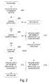
- FIG. 2is a flowchart generally illustrating an embodiment of a process for reading a page of data from a memory device.
- FIG. 3is a flowchart generally illustrating an embodiment of a process for proactive retirement of a degraded block.
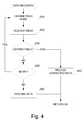
- FIG. 4is a flowchart generally illustrating an embodiment of a process for recovering data determined to have uncorrectable errors.
- Apparatus and methodsread data from non-volatile integrated circuit memory devices, such as NAND flash. For example, these techniques can be embodied in a device driver of an operating system. At least a partial history of errors is maintained (e.g., tracked) during read operations. Read operations for a page typically occur much more frequently than erase operations for the corresponding block or programming of the page. The errors encountered and tracked during these read operations can provide an indication of the reliability of the page and block being read.
- the blockis then indicated (e.g.,designated) for retirement.
- the blockcan be retired, for example, by adding the block to a bad block table when it is requested to be erased or written (programmed).
- One embodimentincludes a technique to recover data from uncorrectable errors. For example, a read mode can be changed to a more reliable read mode to attempt to recover data. This read mode can have less aggressive timing. One embodiment further returns data from the memory device regardless of whether or not the data was corrected by decoding of error correction code data. In contrast to hard disk devices, which typically fail catastrophically, an integrated circuit memory device typically has a small number of bit failures, which leaves most of the data usable even when error correction fails.
- a device driver for an operating system embodying the disclosed techniquescan be embodied in software (in code), in hardware (in modules), or in a combination of software and hardware.
- softwarein code
- hardwarein modules
- softwarein a combination of software and hardware.
- principles and advantages described hereinwill be applicable to other forms of non-volatile integrated circuits as well.
- Other embodiments of the invention, including embodiments that do not provide all of the benefits and features set forth herein,will be apparent to those of ordinary skill in the art.
- FIG. 2is a flowchart generally illustrating a process for reading a page of data from a memory device 106 ( FIG. 1 ) and maintaining a history of errors.
- the processis performed by the device driver 110 ( FIG. 1 ) of an operating system, and the memory device 106 is a NAND flash memory device.
- the illustrated processcan be modified in a variety of ways. For example, in another embodiment, various portions of the illustrated process can be combined, can be rearranged in an alternate sequence, can be removed, and the like. At the start of the process, it is assumed that data has already been stored in the memory device along with corresponding error correction code data.
- a counteris used to maintain the history of errors for the block.
- the memory device 106has many blocks and can have one counter per block for the tracking of errors.
- a counter arrayis used to store the counters.
- MAXwhich can be a predetermined value such as a value of 10
- the processdetermines that the block is to be retired early. For example, the block can be retired when it is to be erased or when a page of the block is to be written as will be described in greater detail later in connection with FIG. 3 .
- Volatile or non-volatile memoriescan be used to store the counters. For robustness, however, it is typically preferred to store this type of information on a different device than the memory device 106 itself.
- the countersare reset to zero upon power up such that the history is reset upon power up. This resetting provides a relatively fast response to a sudden degradation in a block.
- the processbegins by receiving a request for a read of a particular page of the memory device 106 ( FIG. 1 ).
- the requestcan be via a subroutine call from a higher layer of the operating system 104 ( FIG. 1 ) than the device driver 110 ( FIG. 1 ), such as from the file system 108 ( FIG. 1 ).
- the processrequests 202 the particular page using low-level instructions, such as machine code to allow the CPU 102 to communicate with the memory device 106 or instructions for the CPU 102 to instruct the DMA controller 116 to communicate with the memory device 106 .
- the memory device 106internally accesses the memory array(s) and provides data for the page.
- the ECC datais decoded to detect whether there were any errors and also to correct errors, should errors exist and be correctable.
- the decoding of ECCcan be a software function or a hardware function. In one embodiment, the encoding and decoding of ECC is a function performed by the device driver 110 . In an alternative embodiment, the encoding and decoding of ECC is a function of the DMA controller 116 .
- the processdetermines 204 whether or not one or more errors were detected when the page was read. Errors can be correctable or not. If no error was encountered during the error detection process, the process proceeds to exit (without updating a counter for the block corresponding to the page) and returns a status of “OK” to the calling routine of the device driver 110 ( FIG. 1 ), such as a file system 108 ( FIG. 1 ).
- the requested datais available at an output buffer of the memory device 106 ( FIG. 1 ), at a logical address for a data bus, can be transferred to another location such as to another buffer, or the like.
- the processdetermines 204 that an error(s) has occurred, the process proceeds to determine 206 , whether or not the error(s) is correctable via decoding of the error correction code (ECC) data. If the error(s) is correctable within the limitations of the ECC, the process proceeds to determine 208 the extent to which the error(s) that had been corrected. For example, in one embodiment, the process compares the uncorrected data with the corrected data to obtain a count of the number of error(s). Otherwise, if the errors were too numerous for correction by the error correction code, the process indicates the block for early retirement 210 . In one embodiment, the counter is set 210 to the threshold value, MAX, to provide the indication of early retirement. Indicating that a block is to be retired early is not the same as actually retiring the block.
- ECCerror correction code
- a blockcan be retired by marking the block as bad, such as by adding the block to a bad block table.
- the bad block tableis typically stored on the memory device 106 ( FIG. 1 ) itself. However, until data from the block is no longer desired, the block should not yet be marked as bad. Marking of the block as bad will prevent read access to the block. Accordingly, in one embodiment, the process waits until an erase operation is requested or a write operation is requested to mark the block as bad, as will be described in greater later in connection with FIG. 3 . In one embodiment, the process returns an error to a calling routine, such as a file system 108 ( FIG. 1 ), which then initiates procedures to retire the block.
- a calling routinesuch as a file system 108 ( FIG. 1 )
- the processadvances from the indicate early retirement state 210 to a data recovery process to attempt to recover the data.
- a data recovery processwill be described in greater detail later in connection with FIG. 4 .
- the processadvances from the indicate early retirement state 210 and returns a “read error” status to the calling routine of the device driver, such as the file system 108 ( FIG. 1 ), and exits.
- the processdetermines 208 the extent to which the ECC corrected the error(s).
- the number of errors that are considered to be relatively few or relatively manycan depend on the page size and the characteristics of the particular memory device 106 ( FIG. 1 ). Appropriate thresholds will be readily determined by one of ordinary skill in the art.
- the illustrated determination 208is binary, i.e., two possible decisions, it will be understood that one or more intermediate levels can also be used.
- the processincrements the counter by a count of 1 for the particular block of the page being read.
- a counter arraycan store various counts for the multiple blocks of the memory device 106 ( FIG. 1 ), e.g., one counter per block of the memory device 106 . As a block contains many pages, errors from multiple pages can contribute to the count for a particular block.
- the processthen proceeds to return a status of “OK” to the calling routine, e.g., the file system 108 ( FIG. 1 ), of the device driver 110 ( FIG. 1 ) and exits.
- the count stored in the counter for the blockwill increase. The count stores a history of errors encountered while reading page(s) of the block.
- the processupdates the counter to designate the block for early retirement.
- the countercan be set to the threshold level, MAX, as described in connection with the state 210 .
- the state 210 and the state 214each set the counter to the threshold level, MAX, to designate the block for early retirement.
- the state 214adjusts the counter by an increment that is equal to or larger than the increment of the state 212 , but potentially smaller than a jump in counter value from the state 210 .
- the processthen proceeds to return a status of “OK” to the calling routine, e.g., the file system 108 ( FIG. 1 ), of the device driver 110 ( FIG. 1 ) and exits.
- the process illustrated in FIG. 2identifies blocks that are degrading and should be retired. It can be advantageous for reliability purposes to recognize degrading blocks relatively early, such as when data is being read from a block, rather than relatively late, such as when new data is being written to the block.
- FIG. 3is a flowchart generally illustrating a process for the proactive retirement of a degraded block.
- the processis performed by a device driver of an operating system, and the memory device is a NAND flash memory device.
- the illustrated processcan be modified in a variety of ways. For example, in another embodiment, various portions of the illustrated process can be combined, can be rearranged in an alternate sequence, can be removed, or the like.
- a NAND flash memorywhile reading or writing is performed at the page level, erasing is performed at the block level.
- the processis initiated by a request to erase a block from the memory device or by a request to write to a page of a block.
- the requestcan come from the file system 108 ( FIG. 1 ) of the operating system 104 ( FIG. 1 ).
- the requestcan be in the context of updating data, can be for deleting data, can be for formatting, or the like.
- the processretrieves 310 an error history associated with the block to be erased or the corresponding block of the page to be written.
- the error historycan be the count described earlier in connection with FIG. 2 .
- the processproceeds to determine whether the block is reliable 320 . If the block is deemed to be reliable, the process proceeds to instruct the memory device 106 ( FIG. 1 ) to erase 330 the block. The process determines 350 whether or not an error occurred during the erasing process or the writing process within the memory device 106 . Assuming that the memory device 106 erases the block or writes to the page without error, the process then exits with a status of “OK” for the calling routine, such as the file system 108 ( FIG. 1 ). If there is an error in the erase or write process, such as stuck bits, then the process can exit with an error status.
- the processproceeds to refuse 360 the requested erase or write operation and exits with an error status, such as an I/O error.
- an error statussuch as an I/O error.
- the blockcan be deemed to be unreliable if the counter is at or above the threshold value for identification of a potentially unreliable block.
- a higher layer calling routinesuch as the file system 108 ( FIG. 1 ) can then reclaim previously written pages, if any, of the block before requesting the device driver 110 ( FIG. 1 ) to mark the block as bad.
- the previously written pages as well as a current page to be writtencan be written to a different block. After a block is marked as bad, the block is not usable.
- marking a block as badis accomplished by adding the block to a bad block table in the memory device 106 ( FIG. 1 ).
- the addition of the block to the bad block tableis also handled by the device driver 110 ( FIG. 1 ) at the request of the file system 108 .
- the early retirement of the blockcan advantageously permit the block to be retired before the block goes bad. This can help to avoid the future loss of data.
- FIG. 4is a flowchart generally illustrating a process for recovering data determined to have uncorrectable errors.
- the processis performed by a device driver 110 ( FIG. 1 ) of an operating system 104 ( FIG. 1 ), and the memory device 106 ( FIG. 1 ) is a NAND flash memory device.
- the illustrated processcan be modified in a variety of ways. For example, in another embodiment, various portions of the illustrated process can be combined, can be rearranged in an alternate sequence, can be removed, and the like.
- the processstarts when a data read from the memory device resulted in uncorrectable errors.
- An uncorrectable errorcan result when there are too many errors for the error correction codes (ECC) to correct.
- ECCerror correction codes
- the processcan begin following the indicate early retirement state 210 of FIG. 2 .
- the processchanges a read mode of operation to attempt to read the data in a correctable manner.
- Most computer systemsare configured to access memory devices, such as the memory device 106 ( FIG. 1 ) at the highest compatible speed during normal operation (fast read mode).
- the read mode of operationis changed to a reliable read mode. This can include, for example, slower bus speeds, longer latencies, or the like.
- the read modecan be changed from a direct memory access (DMA) mode to a mode using the microprocessor to control access, which is also known as processor input/output or PIO.
- DMAdirect memory access
- the DMA modeis preferred because its use frees up the microprocessor to perform other tasks.
- the microprocessorcan perform a read operation with more control than with DMA.
- the processcan request the temporary disabling of a device that generates noise, such as a speaker of a cell phone.
- the processcan deliberately slow down timing for the memory device 106 .
- Other techniqueswill be readily determined by one of ordinary skill in the art. Various features of these techniques can also be combined.
- the processproceeds to request a read 420 of the page previously read from the memory device. This read corresponds to a re-read.
- the error correction code dataare also retrieved and reapplied to determine 430 if the data is now correctable. In many circumstances, the data can be correctable after the read using a more reliable mode. If the data is correctable, the process proceeds to provide 440 the corrected data, and the process exits with a status of “OK.”
- the processdetermines 450 whether to retry or to provide data 460 with errors.
- the determination 450 to retry or to provide datacan be based on, for example, a loop counter, a timer, and the like.
- the processcan return to the state 410 or the read state 420 to re-read data. If the process returns to the state 410 , a different (e.g., third, fourth, etc.) read mode can also be tried. For example, if more than one reliable read mode exists, the features of various read modes can be tried separately and/or in combination.
- one embodimentnevertheless provides data 460 with the errors.
- errors in solid-state devicessuch as NAND flash are often characterized by single-bit failures. While the number of errors will typically be greater than one bit when the page is uncorrectable, the return of data having an error can be better than no return of data. For example, in many instances, the portion of the data with the error will be unnoticeable. For example, if program code is stored in the page, the portion with the error can correspond to a portion of the code that is not always executed. By contrast, when no data is provided, then the entire page's data is not available, in which case, a program nearly always crashes.
- One embodimentis a method of monitoring a block of a non-volatile integrated circuit memory device, wherein the method includes: decoding error correction codes to determine whether or not a page of data of the block of the memory device was read with at least one error; and maintaining a history of errors for the block of the memory device corresponding to the page that was read at least when the page was read with at least one error, wherein the history of errors is used to indicate whether or not to retire the block early.
- One embodimentis a method of managing blocks for a non-volatile integrated circuit memory device, wherein the method includes: receiving a command to erase a block of memory or write to a page of the block of memory; and disabling an erase or write based at least in part on a history of errors associated with read operations for one or more pages of the block.
- One embodimentis a method of accessing a page of data from a non-volatile integrated circuit memory device, wherein the method includes: requesting a read of the page of data from the memory device; inspecting error correction codes (ECC) associated with the page; and providing a status to an operating system that indicates that the page of data was read correctly regardless of whether or not the page of data included any uncorrectable errors.
- ECCerror correction codes
- One embodimentis a method of maintaining one or more indications for indicating that a block of a non-volatile integrated circuit memory device, wherein the method includes preventing further erasing or reprogramming of the block at least partially in response to at least one of: determining that an error detected as part of at least one read operation performed with respect to at least one page of the block of memory is not correctable via decoding of an error correction code; or determining that a history of errors collected for the blocks of the memory device indicates that at least one error has occurred during a prior read operation for the block.
- One embodimentis an apparatus for monitoring a block of a non-volatile integrated circuit memory device, wherein the apparatus includes: a module configured to decode error correction codes to determine whether or not a page of data of the block of the memory device was read with at least one error; and a module configured to maintain a history of errors for the block of the memory device corresponding to the page that was read at least when the page was read with at least one error, wherein the history of errors is used to indicate whether or not to retire the block early.
Landscapes
- Engineering & Computer Science (AREA)
- Theoretical Computer Science (AREA)
- Quality & Reliability (AREA)
- Physics & Mathematics (AREA)
- General Engineering & Computer Science (AREA)
- General Physics & Mathematics (AREA)
- Techniques For Improving Reliability Of Storages (AREA)
- Read Only Memory (AREA)
- Dram (AREA)
Abstract
Description
Claims (16)
Priority Applications (15)
| Application Number | Priority Date | Filing Date | Title |
|---|---|---|---|
| US11/759,585US7765426B2 (en) | 2007-06-07 | 2007-06-07 | Emerging bad block detection |
| JP2010511237AJP2010529557A (en) | 2007-06-07 | 2008-05-16 | New bad block detection |
| CN200880018929XACN101681281B (en) | 2007-06-07 | 2008-05-16 | detect bad blocks |
| KR1020147030099AKR101557736B1 (en) | 2007-06-07 | 2008-05-16 | Emerging bad block detection |
| PCT/US2008/063938WO2008154119A1 (en) | 2007-06-07 | 2008-05-16 | Emerging bad block detection |
| CN201210298956.5ACN102880521B (en) | 2007-06-07 | 2008-05-16 | The method and apparatus of management block and access data page in non-volatile memory device |
| AT08755737TATE514131T1 (en) | 2007-06-07 | 2008-05-16 | DETECTION OF UPCOMING BAD BLOCKS |
| KR1020107000248AKR101522744B1 (en) | 2007-06-07 | 2008-05-16 | Emerging bad block detection |
| EP20110165727EP2367110B1 (en) | 2007-06-07 | 2008-05-16 | Emerging bad block detection |
| EP20110165755EP2372549B1 (en) | 2007-06-07 | 2008-05-16 | Emerging bad block detection |
| EP20080755737EP2162822B1 (en) | 2007-06-07 | 2008-05-16 | Emerging bad block detection |
| TW097119742ATWI370355B (en) | 2007-06-07 | 2008-05-28 | Method and apparatus of monitoring a block of a non-volatile integrated circuit memory device,method of amanaging blocks for a non-volatile integrated circuit memory device and method of accessing page of data for a page of data from a non-volatile integ |
| US12/839,048US7954004B2 (en) | 2007-06-07 | 2010-07-19 | Systems and methods for retrieving data |
| US13/116,407US8930771B2 (en) | 2007-06-07 | 2011-05-26 | Systems and methods for retrieving data |
| US14/588,869US9405639B2 (en) | 2007-06-07 | 2015-01-02 | Systems and methods for retrieving data |
Applications Claiming Priority (1)
| Application Number | Priority Date | Filing Date | Title |
|---|---|---|---|
| US11/759,585US7765426B2 (en) | 2007-06-07 | 2007-06-07 | Emerging bad block detection |
Related Child Applications (1)
| Application Number | Title | Priority Date | Filing Date |
|---|---|---|---|
| US12/839,048DivisionUS7954004B2 (en) | 2007-06-07 | 2010-07-19 | Systems and methods for retrieving data |
Publications (2)
| Publication Number | Publication Date |
|---|---|
| US20080307270A1 US20080307270A1 (en) | 2008-12-11 |
| US7765426B2true US7765426B2 (en) | 2010-07-27 |
Family
ID=39628943
Family Applications (4)
| Application Number | Title | Priority Date | Filing Date |
|---|---|---|---|
| US11/759,585Active2028-05-22US7765426B2 (en) | 2007-06-07 | 2007-06-07 | Emerging bad block detection |
| US12/839,048ActiveUS7954004B2 (en) | 2007-06-07 | 2010-07-19 | Systems and methods for retrieving data |
| US13/116,407Active2028-04-13US8930771B2 (en) | 2007-06-07 | 2011-05-26 | Systems and methods for retrieving data |
| US14/588,869ActiveUS9405639B2 (en) | 2007-06-07 | 2015-01-02 | Systems and methods for retrieving data |
Family Applications After (3)
| Application Number | Title | Priority Date | Filing Date |
|---|---|---|---|
| US12/839,048ActiveUS7954004B2 (en) | 2007-06-07 | 2010-07-19 | Systems and methods for retrieving data |
| US13/116,407Active2028-04-13US8930771B2 (en) | 2007-06-07 | 2011-05-26 | Systems and methods for retrieving data |
| US14/588,869ActiveUS9405639B2 (en) | 2007-06-07 | 2015-01-02 | Systems and methods for retrieving data |
Country Status (8)
| Country | Link |
|---|---|
| US (4) | US7765426B2 (en) |
| EP (3) | EP2372549B1 (en) |
| JP (1) | JP2010529557A (en) |
| KR (2) | KR101557736B1 (en) |
| CN (2) | CN101681281B (en) |
| AT (1) | ATE514131T1 (en) |
| TW (1) | TWI370355B (en) |
| WO (1) | WO2008154119A1 (en) |
Cited By (27)
| Publication number | Priority date | Publication date | Assignee | Title |
|---|---|---|---|---|
| US20090055578A1 (en)* | 2007-08-24 | 2009-02-26 | Samsung Electronics Co., Ltd. | Apparatus using flash memory as storage and method of operating the same |
| US20090125782A1 (en)* | 2007-11-12 | 2009-05-14 | Harris Corporation | Memory system and related method using software-defined radio with write-protected, non-volatile memory |
| US20100064187A1 (en)* | 2008-09-11 | 2010-03-11 | Mediatek Inc. | Bad block identification methods |
| US20100100763A1 (en)* | 2008-10-16 | 2010-04-22 | Genesys Logic, Inc. | Flash memory controller having configuring unit for error correction code (ecc) capability and method thereof |
| US20100122148A1 (en)* | 2008-11-10 | 2010-05-13 | David Flynn | Apparatus, system, and method for predicting failures in solid-state storage |
| US20100332942A1 (en)* | 2008-09-10 | 2010-12-30 | Arm Limited | Memory controller for NAND memory using forward error correction |
| US20110047421A1 (en)* | 2009-08-24 | 2011-02-24 | Ocz Technology Group, Inc. | Nand flash-based storage device with built-in test-ahead for failure anticipation |
| US20110087950A1 (en)* | 2009-10-12 | 2011-04-14 | Phison Electronics Corp. | Data writing method for a flash memory, and controller and storage system using the same |
| US20110230711A1 (en)* | 2010-03-16 | 2011-09-22 | Kano Akihito | Endoscopic Surgical Instrument |
| US20110239061A1 (en)* | 2007-06-07 | 2011-09-29 | Micron Technology, Inc. | Systems and methods for retrieving data |
| US20140068377A1 (en)* | 2012-08-30 | 2014-03-06 | SK Hynix Inc. | Semiconductor memory device and method of operating the same |
| US8689082B2 (en) | 2011-07-28 | 2014-04-01 | Samsung Electronics Co., Ltd. | Method of operating memory controller, and memory system, memory card and portable electronic device including the memory controller |
| US20140164824A1 (en)* | 2009-10-27 | 2014-06-12 | Micron Technology, Inc. | Error detection/correction based memory management |
| US20140380129A1 (en)* | 2013-06-24 | 2014-12-25 | Samsung Electronics Co., Ltd. | Memory system and method of reading data thereof |
| US8934304B2 (en) | 2011-05-16 | 2015-01-13 | Samsung Electronics Co., Ltd. | Operating method of nonvolatile memory device and operating method of memory system including nonvolatile memory device |
| US9063874B2 (en) | 2008-11-10 | 2015-06-23 | SanDisk Technologies, Inc. | Apparatus, system, and method for wear management |
| US20150212871A1 (en)* | 2013-03-14 | 2015-07-30 | Micron Technology, Inc. | Selective reading of memory with improved accuracy |
| US9170897B2 (en) | 2012-05-29 | 2015-10-27 | SanDisk Technologies, Inc. | Apparatus, system, and method for managing solid-state storage reliability |
| US9213594B2 (en) | 2011-01-19 | 2015-12-15 | Intelligent Intellectual Property Holdings 2 Llc | Apparatus, system, and method for managing out-of-service conditions |
| US9443616B2 (en)* | 2014-04-02 | 2016-09-13 | Seagate Technology Llc | Bad memory unit detection in a solid state drive |
| US9678874B2 (en) | 2011-01-31 | 2017-06-13 | Sandisk Technologies Llc | Apparatus, system, and method for managing eviction of data |
| US9767032B2 (en) | 2012-01-12 | 2017-09-19 | Sandisk Technologies Llc | Systems and methods for cache endurance |
| US10019352B2 (en) | 2013-10-18 | 2018-07-10 | Sandisk Technologies Llc | Systems and methods for adaptive reserve storage |
| US10146604B2 (en)* | 2016-08-23 | 2018-12-04 | Oracle International Corporation | Bad block detection and predictive analytics in NAND flash storage devices |
| US20190294346A1 (en)* | 2018-03-26 | 2019-09-26 | International Business Machines Corporation | Limiting simultaneous failure of multiple storage devices |
| US20220027464A1 (en)* | 2020-07-23 | 2022-01-27 | Nxp Usa, Inc. | Systems and methods for constraining access to one time programmable storage elements |
| US11853583B2 (en) | 2018-09-13 | 2023-12-26 | Kioxia Corporation | Pool-level storage management |
Families Citing this family (233)
| Publication number | Priority date | Publication date | Assignee | Title |
|---|---|---|---|---|
| KR101413736B1 (en)* | 2007-09-13 | 2014-07-02 | 삼성전자주식회사 | Memory system with improved reliability and wear-leveling technique thereof |
| TW200919448A (en)* | 2007-10-17 | 2009-05-01 | Silicon Motion Inc | Storage device and method of accessing a status thereof |
| TWI381390B (en)* | 2008-04-10 | 2013-01-01 | Phison Electronics Corp | Bad block determining method for flash memory, storage system and controller thereof |
| US9449719B2 (en)* | 2008-12-19 | 2016-09-20 | Seagate Technology Llc | Solid-state storage device including a high resolution analog-to-digital converter |
| EP2307960B1 (en)* | 2009-04-21 | 2018-01-10 | Avago Technologies General IP (Singapore) Pte. Ltd. | Error-floor mitigation of codes using write verification |
| US8151137B2 (en)* | 2009-05-28 | 2012-04-03 | Lsi Corporation | Systems and methods for governing the life cycle of a solid state drive |
| US8176367B2 (en) | 2009-05-28 | 2012-05-08 | Agere Systems Inc. | Systems and methods for managing end of life in a solid state drive |
| US8549384B1 (en)* | 2009-06-26 | 2013-10-01 | Marvell International Ltd. | Method and apparatus for determining, based on an error correction code, one or more locations to store data in a flash memory |
| US8321727B2 (en)* | 2009-06-29 | 2012-11-27 | Sandisk Technologies Inc. | System and method responsive to a rate of change of a performance parameter of a memory |
| KR101678909B1 (en)* | 2009-09-17 | 2016-11-23 | 삼성전자주식회사 | Flash memory system and erase refresh methods for the same |
| US8429468B2 (en)* | 2010-01-27 | 2013-04-23 | Sandisk Technologies Inc. | System and method to correct data errors using a stored count of bit values |
| US8327226B2 (en)* | 2010-02-03 | 2012-12-04 | Seagate Technology Llc | Adjustable error correction code length in an electrical storage device |
| US8341339B1 (en) | 2010-06-14 | 2012-12-25 | Western Digital Technologies, Inc. | Hybrid drive garbage collecting a non-volatile semiconductor memory by migrating valid data to a disk |
| US8959284B1 (en) | 2010-06-28 | 2015-02-17 | Western Digital Technologies, Inc. | Disk drive steering write data to write cache based on workload |
| US9146875B1 (en) | 2010-08-09 | 2015-09-29 | Western Digital Technologies, Inc. | Hybrid drive converting non-volatile semiconductor memory to read only based on life remaining |
| US9058280B1 (en) | 2010-08-13 | 2015-06-16 | Western Digital Technologies, Inc. | Hybrid drive migrating data from disk to non-volatile semiconductor memory based on accumulated access time |
| US8639872B1 (en) | 2010-08-13 | 2014-01-28 | Western Digital Technologies, Inc. | Hybrid drive comprising write cache spanning non-volatile semiconductor memory and disk |
| US9268499B1 (en) | 2010-08-13 | 2016-02-23 | Western Digital Technologies, Inc. | Hybrid drive migrating high workload data from disk to non-volatile semiconductor memory |
| US8683295B1 (en) | 2010-08-31 | 2014-03-25 | Western Digital Technologies, Inc. | Hybrid drive writing extended error correction code symbols to disk for data sectors stored in non-volatile semiconductor memory |
| US8775720B1 (en) | 2010-08-31 | 2014-07-08 | Western Digital Technologies, Inc. | Hybrid drive balancing execution times for non-volatile semiconductor memory and disk |
| US8782334B1 (en) | 2010-09-10 | 2014-07-15 | Western Digital Technologies, Inc. | Hybrid drive copying disk cache to non-volatile semiconductor memory |
| US8589655B2 (en) | 2010-09-15 | 2013-11-19 | Pure Storage, Inc. | Scheduling of I/O in an SSD environment |
| US8589625B2 (en) | 2010-09-15 | 2013-11-19 | Pure Storage, Inc. | Scheduling of reconstructive I/O read operations in a storage environment |
| US11614893B2 (en) | 2010-09-15 | 2023-03-28 | Pure Storage, Inc. | Optimizing storage device access based on latency |
| US8468318B2 (en) | 2010-09-15 | 2013-06-18 | Pure Storage Inc. | Scheduling of I/O writes in a storage environment |
| US11275509B1 (en) | 2010-09-15 | 2022-03-15 | Pure Storage, Inc. | Intelligently sizing high latency I/O requests in a storage environment |
| US12008266B2 (en) | 2010-09-15 | 2024-06-11 | Pure Storage, Inc. | Efficient read by reconstruction |
| US8732426B2 (en) | 2010-09-15 | 2014-05-20 | Pure Storage, Inc. | Scheduling of reactive I/O operations in a storage environment |
| US9244769B2 (en) | 2010-09-28 | 2016-01-26 | Pure Storage, Inc. | Offset protection data in a RAID array |
| US8825976B1 (en) | 2010-09-28 | 2014-09-02 | Western Digital Technologies, Inc. | Hybrid drive executing biased migration policy during host boot to migrate data to a non-volatile semiconductor memory |
| US8775868B2 (en) | 2010-09-28 | 2014-07-08 | Pure Storage, Inc. | Adaptive RAID for an SSD environment |
| US8825977B1 (en)* | 2010-09-28 | 2014-09-02 | Western Digital Technologies, Inc. | Hybrid drive writing copy of data to disk when non-volatile semiconductor memory nears end of life |
| US8670205B1 (en) | 2010-09-29 | 2014-03-11 | Western Digital Technologies, Inc. | Hybrid drive changing power mode of disk channel when frequency of write data exceeds a threshold |
| US8699171B1 (en) | 2010-09-30 | 2014-04-15 | Western Digital Technologies, Inc. | Disk drive selecting head for write operation based on environmental condition |
| US8612798B1 (en) | 2010-10-21 | 2013-12-17 | Western Digital Technologies, Inc. | Hybrid drive storing write data in non-volatile semiconductor memory if write verify of disk fails |
| US8429343B1 (en) | 2010-10-21 | 2013-04-23 | Western Digital Technologies, Inc. | Hybrid drive employing non-volatile semiconductor memory to facilitate refreshing disk |
| US8427771B1 (en) | 2010-10-21 | 2013-04-23 | Western Digital Technologies, Inc. | Hybrid drive storing copy of data in non-volatile semiconductor memory for suspect disk data sectors |
| US8560759B1 (en) | 2010-10-25 | 2013-10-15 | Western Digital Technologies, Inc. | Hybrid drive storing redundant copies of data on disk and in non-volatile semiconductor memory based on read frequency |
| US9069475B1 (en) | 2010-10-26 | 2015-06-30 | Western Digital Technologies, Inc. | Hybrid drive selectively spinning up disk when powered on |
| US8649215B2 (en) | 2010-12-22 | 2014-02-11 | HGST Netherlands B.V. | Data management in flash memory using probability of charge disturbances |
| US8422296B2 (en) | 2010-12-22 | 2013-04-16 | HGST Netherlands B.V. | Early detection of degradation in NAND flash memory |
| US8599609B2 (en) | 2010-12-22 | 2013-12-03 | HGST Netherlands B.V. | Data management in flash memory using probability of charge disturbances |
| US8422303B2 (en) | 2010-12-22 | 2013-04-16 | HGST Netherlands B.V. | Early degradation detection in flash memory using test cells |
| US8369143B2 (en) | 2010-12-22 | 2013-02-05 | HGST Netherlands B.V. | Early detection of degradation in NOR flash memory |
| IT1403899B1 (en)* | 2010-12-30 | 2013-11-08 | Incard Sa | METHOD AND SYSTEM TO CHECK THE LOSS OF RELIABILITY OF A NON-VOLATILE MEMORY |
| KR101739878B1 (en)* | 2011-02-22 | 2017-05-26 | 삼성전자주식회사 | Controller, method of operating the controller, and memory system having the controller |
| US8560922B2 (en) | 2011-03-04 | 2013-10-15 | International Business Machines Corporation | Bad block management for flash memory |
| TW201239893A (en)* | 2011-03-25 | 2012-10-01 | Silicon Motion Inc | Method for enhancing data protection performance, and associated personal computer and storage medium |
| US9086983B2 (en)* | 2011-05-31 | 2015-07-21 | Micron Technology, Inc. | Apparatus and methods for providing data integrity |
| US8693252B2 (en) | 2011-07-12 | 2014-04-08 | Samsung Electronics Co., Ltd. | Method and system for adjusting read voltage in flash memory device |
| US11636031B2 (en) | 2011-08-11 | 2023-04-25 | Pure Storage, Inc. | Optimized inline deduplication |
| US8589640B2 (en) | 2011-10-14 | 2013-11-19 | Pure Storage, Inc. | Method for maintaining multiple fingerprint tables in a deduplicating storage system |
| US8630056B1 (en) | 2011-09-12 | 2014-01-14 | Western Digital Technologies, Inc. | Hybrid drive adjusting spin-up profile based on cache status of non-volatile semiconductor memory |
| US8909889B1 (en) | 2011-10-10 | 2014-12-09 | Western Digital Technologies, Inc. | Method and apparatus for servicing host commands by a disk drive |
| US8977804B1 (en) | 2011-11-21 | 2015-03-10 | Western Digital Technologies, Inc. | Varying data redundancy in storage systems |
| US9268701B1 (en) | 2011-11-21 | 2016-02-23 | Western Digital Technologies, Inc. | Caching of data in data storage systems by managing the size of read and write cache based on a measurement of cache reliability |
| US8977803B2 (en) | 2011-11-21 | 2015-03-10 | Western Digital Technologies, Inc. | Disk drive data caching using a multi-tiered memory |
| US8904091B1 (en) | 2011-12-22 | 2014-12-02 | Western Digital Technologies, Inc. | High performance media transport manager architecture for data storage systems |
| US8719540B1 (en) | 2012-03-15 | 2014-05-06 | Pure Storage, Inc. | Fractal layout of data blocks across multiple devices |
| US9047187B2 (en)* | 2012-06-28 | 2015-06-02 | Intel Corporation | Defect management in memory systems |
| CN103631721A (en)* | 2012-08-23 | 2014-03-12 | 华为技术有限公司 | Method and system for isolating bad blocks in internal storage |
| US8793558B2 (en)* | 2012-08-27 | 2014-07-29 | Freescale Semiconductor, Inc. | Adaptive error correction for non-volatile memories |
| US8930776B2 (en) | 2012-08-29 | 2015-01-06 | International Business Machines Corporation | Implementing DRAM command timing adjustments to alleviate DRAM failures |
| US11032259B1 (en) | 2012-09-26 | 2021-06-08 | Pure Storage, Inc. | Data protection in a storage system |
| US10623386B1 (en) | 2012-09-26 | 2020-04-14 | Pure Storage, Inc. | Secret sharing data protection in a storage system |
| US8745415B2 (en) | 2012-09-26 | 2014-06-03 | Pure Storage, Inc. | Multi-drive cooperation to generate an encryption key |
| JP2014086062A (en)* | 2012-10-29 | 2014-05-12 | Sony Corp | Storage control device, storage, information processing system and storage control method |
| US8959281B1 (en) | 2012-11-09 | 2015-02-17 | Western Digital Technologies, Inc. | Data management for a storage device |
| US8935592B2 (en)* | 2012-11-20 | 2015-01-13 | Arm Limited | Apparatus and method for correcting errors in data accessed from a memory device |
| US9116822B2 (en) | 2012-12-07 | 2015-08-25 | Micron Technology, Inc. | Stopping criteria for layered iterative error correction |
| US10908835B1 (en) | 2013-01-10 | 2021-02-02 | Pure Storage, Inc. | Reversing deletion of a virtual machine |
| US11768623B2 (en) | 2013-01-10 | 2023-09-26 | Pure Storage, Inc. | Optimizing generalized transfers between storage systems |
| US9063967B2 (en) | 2013-01-10 | 2015-06-23 | Pure Storage, Inc. | Performing copies in a storage system |
| US11733908B2 (en) | 2013-01-10 | 2023-08-22 | Pure Storage, Inc. | Delaying deletion of a dataset |
| CN103116550A (en)* | 2013-01-11 | 2013-05-22 | 深圳市硅格半导体有限公司 | Method and device for switching physical block work mode in flash memory |
| US9690953B2 (en)* | 2013-03-14 | 2017-06-27 | Apple Inc. | Generating efficient reads for a system having non-volatile memory |
| CN105408869B (en)* | 2013-05-29 | 2018-12-25 | 慧与发展有限责任合伙企业 | Call error processing routine handles the mistake that can not be corrected |
| US9141176B1 (en) | 2013-07-29 | 2015-09-22 | Western Digital Technologies, Inc. | Power management for data storage device |
| US9070379B2 (en) | 2013-08-28 | 2015-06-30 | Western Digital Technologies, Inc. | Data migration for data storage device |
| US9164828B2 (en) | 2013-09-26 | 2015-10-20 | Seagate Technology Llc | Systems and methods for enhanced data recovery in a solid state memory system |
| US9424179B2 (en) | 2013-10-17 | 2016-08-23 | Seagate Technology Llc | Systems and methods for latency based data recycling in a solid state memory system |
| US9201729B2 (en) | 2013-10-21 | 2015-12-01 | Seagate Technology, Llc | Systems and methods for soft data utilization in a solid state memory system |
| US9378840B2 (en) | 2013-10-28 | 2016-06-28 | Seagate Technology Llc | Systems and methods for sub-zero threshold characterization in a memory cell |
| US9323467B2 (en) | 2013-10-29 | 2016-04-26 | Western Digital Technologies, Inc. | Data storage device startup |
| US8917471B1 (en) | 2013-10-29 | 2014-12-23 | Western Digital Technologies, Inc. | Power management for data storage device |
| US11128448B1 (en) | 2013-11-06 | 2021-09-21 | Pure Storage, Inc. | Quorum-aware secret sharing |
| US10263770B2 (en) | 2013-11-06 | 2019-04-16 | Pure Storage, Inc. | Data protection in a storage system using external secrets |
| US10365858B2 (en) | 2013-11-06 | 2019-07-30 | Pure Storage, Inc. | Thin provisioning in a storage device |
| US9276609B2 (en) | 2013-11-16 | 2016-03-01 | Seagate Technology Llc | Systems and methods for soft decision generation in a solid state memory system |
| US9389937B2 (en) | 2013-11-19 | 2016-07-12 | Lenovo Enterprise Solutions (Singapore) Pte. Ltd. | Managing faulty memory pages in a computing system |
| US9208086B1 (en) | 2014-01-09 | 2015-12-08 | Pure Storage, Inc. | Using frequency domain to prioritize storage of metadata in a cache |
| US9576683B2 (en) | 2014-02-06 | 2017-02-21 | Seagate Technology Llc | Systems and methods for hard error reduction in a solid state memory device |
| US9378810B2 (en) | 2014-02-11 | 2016-06-28 | Seagate Technology Llc | Systems and methods for last written page handling in a memory device |
| US10656864B2 (en) | 2014-03-20 | 2020-05-19 | Pure Storage, Inc. | Data replication within a flash storage array |
| US9431129B2 (en)* | 2014-04-30 | 2016-08-30 | Qualcomm Incorporated | Variable read delay system |
| US9779268B1 (en) | 2014-06-03 | 2017-10-03 | Pure Storage, Inc. | Utilizing a non-repeating identifier to encrypt data |
| US11399063B2 (en) | 2014-06-04 | 2022-07-26 | Pure Storage, Inc. | Network authentication for a storage system |
| US9218244B1 (en) | 2014-06-04 | 2015-12-22 | Pure Storage, Inc. | Rebuilding data across storage nodes |
| US10496556B1 (en) | 2014-06-25 | 2019-12-03 | Pure Storage, Inc. | Dynamic data protection within a flash storage system |
| US9218407B1 (en) | 2014-06-25 | 2015-12-22 | Pure Storage, Inc. | Replication and intermediate read-write state for mediums |
| US10296469B1 (en) | 2014-07-24 | 2019-05-21 | Pure Storage, Inc. | Access control in a flash storage system |
| US9495255B2 (en) | 2014-08-07 | 2016-11-15 | Pure Storage, Inc. | Error recovery in a storage cluster |
| US9558069B2 (en) | 2014-08-07 | 2017-01-31 | Pure Storage, Inc. | Failure mapping in a storage array |
| US9864761B1 (en) | 2014-08-08 | 2018-01-09 | Pure Storage, Inc. | Read optimization operations in a storage system |
| US12175076B2 (en) | 2014-09-08 | 2024-12-24 | Pure Storage, Inc. | Projecting capacity utilization for snapshots |
| US10430079B2 (en) | 2014-09-08 | 2019-10-01 | Pure Storage, Inc. | Adjusting storage capacity in a computing system |
| US10164841B2 (en) | 2014-10-02 | 2018-12-25 | Pure Storage, Inc. | Cloud assist for storage systems |
| US10430282B2 (en) | 2014-10-07 | 2019-10-01 | Pure Storage, Inc. | Optimizing replication by distinguishing user and system write activity |
| US9489132B2 (en) | 2014-10-07 | 2016-11-08 | Pure Storage, Inc. | Utilizing unmapped and unknown states in a replicated storage system |
| US9727485B1 (en) | 2014-11-24 | 2017-08-08 | Pure Storage, Inc. | Metadata rewrite and flatten optimization |
| US9773007B1 (en) | 2014-12-01 | 2017-09-26 | Pure Storage, Inc. | Performance improvements in a storage system |
| US9552248B2 (en) | 2014-12-11 | 2017-01-24 | Pure Storage, Inc. | Cloud alert to replica |
| US9588842B1 (en) | 2014-12-11 | 2017-03-07 | Pure Storage, Inc. | Drive rebuild |
| US9864769B2 (en) | 2014-12-12 | 2018-01-09 | Pure Storage, Inc. | Storing data utilizing repeating pattern detection |
| US10545987B2 (en) | 2014-12-19 | 2020-01-28 | Pure Storage, Inc. | Replication to the cloud |
| US10296354B1 (en) | 2015-01-21 | 2019-05-21 | Pure Storage, Inc. | Optimized boot operations within a flash storage array |
| US11947968B2 (en) | 2015-01-21 | 2024-04-02 | Pure Storage, Inc. | Efficient use of zone in a storage device |
| US9710165B1 (en) | 2015-02-18 | 2017-07-18 | Pure Storage, Inc. | Identifying volume candidates for space reclamation |
| TWI602185B (en)* | 2015-03-04 | 2017-10-11 | 旺宏電子股份有限公司 | Memory device and operating method of the same |
| US10082985B2 (en) | 2015-03-27 | 2018-09-25 | Pure Storage, Inc. | Data striping across storage nodes that are assigned to multiple logical arrays |
| US10178169B2 (en) | 2015-04-09 | 2019-01-08 | Pure Storage, Inc. | Point to point based backend communication layer for storage processing |
| US10652103B2 (en) | 2015-04-24 | 2020-05-12 | Goldman Sachs & Co. LLC | System and method for handling events involving computing systems and networks using fabric monitoring system |
| CN106155585B (en)* | 2015-05-13 | 2020-05-15 | 爱思开海力士有限公司 | Adaptive read disturb recovery strategy |
| US10140149B1 (en) | 2015-05-19 | 2018-11-27 | Pure Storage, Inc. | Transactional commits with hardware assists in remote memory |
| US9547441B1 (en) | 2015-06-23 | 2017-01-17 | Pure Storage, Inc. | Exposing a geometry of a storage device |
| US10310740B2 (en) | 2015-06-23 | 2019-06-04 | Pure Storage, Inc. | Aligning memory access operations to a geometry of a storage device |
| KR20170028825A (en) | 2015-09-04 | 2017-03-14 | 퓨어 스토리지, 아이앤씨. | Memory-efficient storage and searching in hash tables using compressed indexes |
| US11341136B2 (en) | 2015-09-04 | 2022-05-24 | Pure Storage, Inc. | Dynamically resizable structures for approximate membership queries |
| US11269884B2 (en) | 2015-09-04 | 2022-03-08 | Pure Storage, Inc. | Dynamically resizable structures for approximate membership queries |
| US9843453B2 (en) | 2015-10-23 | 2017-12-12 | Pure Storage, Inc. | Authorizing I/O commands with I/O tokens |
| US9417809B1 (en) | 2015-12-07 | 2016-08-16 | International Business Machines Corporation | Efficient management of page retirement in non-volatile memory utilizing page retirement classes |
| US9620227B1 (en)* | 2016-01-08 | 2017-04-11 | Western Digital Technologies, Inc. | Characterizing and operating a non-volatile memory device |
| CN105843700B (en)* | 2016-03-25 | 2019-01-15 | 中国科学院微电子研究所 | Controller |
| TWI576699B (en) | 2016-03-31 | 2017-04-01 | 慧榮科技股份有限公司 | A method for recording an using time of a data block and device thereof |
| US10452297B1 (en) | 2016-05-02 | 2019-10-22 | Pure Storage, Inc. | Generating and optimizing summary index levels in a deduplication storage system |
| US10133503B1 (en) | 2016-05-02 | 2018-11-20 | Pure Storage, Inc. | Selecting a deduplication process based on a difference between performance metrics |
| US10203903B2 (en) | 2016-07-26 | 2019-02-12 | Pure Storage, Inc. | Geometry based, space aware shelf/writegroup evacuation |
| US10162523B2 (en) | 2016-10-04 | 2018-12-25 | Pure Storage, Inc. | Migrating data between volumes using virtual copy operation |
| US10756816B1 (en) | 2016-10-04 | 2020-08-25 | Pure Storage, Inc. | Optimized fibre channel and non-volatile memory express access |
| US10613974B2 (en) | 2016-10-04 | 2020-04-07 | Pure Storage, Inc. | Peer-to-peer non-volatile random-access memory |
| US10191662B2 (en) | 2016-10-04 | 2019-01-29 | Pure Storage, Inc. | Dynamic allocation of segments in a flash storage system |
| US10481798B2 (en) | 2016-10-28 | 2019-11-19 | Pure Storage, Inc. | Efficient flash management for multiple controllers |
| US10185505B1 (en) | 2016-10-28 | 2019-01-22 | Pure Storage, Inc. | Reading a portion of data to replicate a volume based on sequence numbers |
| US10359942B2 (en) | 2016-10-31 | 2019-07-23 | Pure Storage, Inc. | Deduplication aware scalable content placement |
| US10452290B2 (en) | 2016-12-19 | 2019-10-22 | Pure Storage, Inc. | Block consolidation in a direct-mapped flash storage system |
| US11550481B2 (en) | 2016-12-19 | 2023-01-10 | Pure Storage, Inc. | Efficiently writing data in a zoned drive storage system |
| US10204693B2 (en)* | 2016-12-31 | 2019-02-12 | Western Digital Technologies, Inc. | Retiring computer memory blocks |
| US11093146B2 (en) | 2017-01-12 | 2021-08-17 | Pure Storage, Inc. | Automatic load rebalancing of a write group |
| KR102844275B1 (en) | 2017-02-02 | 2025-08-12 | 에스케이하이닉스 주식회사 | Memory system and operating method of memory system |
| JP2018156556A (en)* | 2017-03-21 | 2018-10-04 | 東芝メモリ株式会社 | Computer system and memory device |
| US10528488B1 (en) | 2017-03-30 | 2020-01-07 | Pure Storage, Inc. | Efficient name coding |
| US12045487B2 (en) | 2017-04-21 | 2024-07-23 | Pure Storage, Inc. | Preserving data deduplication in a multi-tenant storage system |
| US11403019B2 (en) | 2017-04-21 | 2022-08-02 | Pure Storage, Inc. | Deduplication-aware per-tenant encryption |
| US10944671B2 (en) | 2017-04-27 | 2021-03-09 | Pure Storage, Inc. | Efficient data forwarding in a networked device |
| US10402266B1 (en) | 2017-07-31 | 2019-09-03 | Pure Storage, Inc. | Redundant array of independent disks in a direct-mapped flash storage system |
| US10831935B2 (en) | 2017-08-31 | 2020-11-10 | Pure Storage, Inc. | Encryption management with host-side data reduction |
| US10776202B1 (en) | 2017-09-22 | 2020-09-15 | Pure Storage, Inc. | Drive, blade, or data shard decommission via RAID geometry shrinkage |
| US10789211B1 (en) | 2017-10-04 | 2020-09-29 | Pure Storage, Inc. | Feature-based deduplication |
| US10884919B2 (en) | 2017-10-31 | 2021-01-05 | Pure Storage, Inc. | Memory management in a storage system |
| US10860475B1 (en) | 2017-11-17 | 2020-12-08 | Pure Storage, Inc. | Hybrid flash translation layer |
| CN108039191A (en)* | 2017-12-20 | 2018-05-15 | 宣城新维保网络技术有限公司 | A kind of memory analog detection method |
| WO2019140074A1 (en) | 2018-01-12 | 2019-07-18 | Micron Technology, Inc | Read retry scratch space |
| US11144638B1 (en) | 2018-01-18 | 2021-10-12 | Pure Storage, Inc. | Method for storage system detection and alerting on potential malicious action |
| US11010233B1 (en) | 2018-01-18 | 2021-05-18 | Pure Storage, Inc | Hardware-based system monitoring |
| US10970395B1 (en) | 2018-01-18 | 2021-04-06 | Pure Storage, Inc | Security threat monitoring for a storage system |
| US10467527B1 (en) | 2018-01-31 | 2019-11-05 | Pure Storage, Inc. | Method and apparatus for artificial intelligence acceleration |
| US11036596B1 (en) | 2018-02-18 | 2021-06-15 | Pure Storage, Inc. | System for delaying acknowledgements on open NAND locations until durability has been confirmed |
| US11494109B1 (en) | 2018-02-22 | 2022-11-08 | Pure Storage, Inc. | Erase block trimming for heterogenous flash memory storage devices |
| US11934322B1 (en) | 2018-04-05 | 2024-03-19 | Pure Storage, Inc. | Multiple encryption keys on storage drives |
| TWI649754B (en)* | 2018-04-16 | 2019-02-01 | 群聯電子股份有限公司 | Memory management method, memory storage device, and memory control circuit unit |
| US11995336B2 (en) | 2018-04-25 | 2024-05-28 | Pure Storage, Inc. | Bucket views |
| US11385792B2 (en) | 2018-04-27 | 2022-07-12 | Pure Storage, Inc. | High availability controller pair transitioning |
| US10678433B1 (en) | 2018-04-27 | 2020-06-09 | Pure Storage, Inc. | Resource-preserving system upgrade |
| US11003537B2 (en) | 2018-05-29 | 2021-05-11 | Micron Technology, Inc. | Determining validity of data read from memory by a controller |
| US10678436B1 (en) | 2018-05-29 | 2020-06-09 | Pure Storage, Inc. | Using a PID controller to opportunistically compress more data during garbage collection |
| US11436023B2 (en) | 2018-05-31 | 2022-09-06 | Pure Storage, Inc. | Mechanism for updating host file system and flash translation layer based on underlying NAND technology |
| US10776046B1 (en) | 2018-06-08 | 2020-09-15 | Pure Storage, Inc. | Optimized non-uniform memory access |
| US11281577B1 (en) | 2018-06-19 | 2022-03-22 | Pure Storage, Inc. | Garbage collection tuning for low drive wear |
| US11869586B2 (en) | 2018-07-11 | 2024-01-09 | Pure Storage, Inc. | Increased data protection by recovering data from partially-failed solid-state devices |
| US11194759B2 (en) | 2018-09-06 | 2021-12-07 | Pure Storage, Inc. | Optimizing local data relocation operations of a storage device of a storage system |
| US11133076B2 (en) | 2018-09-06 | 2021-09-28 | Pure Storage, Inc. | Efficient relocation of data between storage devices of a storage system |
| US10747613B2 (en)* | 2018-09-07 | 2020-08-18 | Toshiba Memory Corporation | Pooled frontline ECC decoders in memory systems |
| US10846216B2 (en) | 2018-10-25 | 2020-11-24 | Pure Storage, Inc. | Scalable garbage collection |
| US11113409B2 (en) | 2018-10-26 | 2021-09-07 | Pure Storage, Inc. | Efficient rekey in a transparent decrypting storage array |
| CN109828894B (en)* | 2018-12-27 | 2022-06-21 | 东软集团股份有限公司 | Device state data collection method, device, storage medium and electronic device |
| US11194473B1 (en) | 2019-01-23 | 2021-12-07 | Pure Storage, Inc. | Programming frequently read data to low latency portions of a solid-state storage array |
| CN111522500A (en)* | 2019-02-01 | 2020-08-11 | 睿宽智能科技有限公司 | Repeat read method |
| US11588633B1 (en) | 2019-03-15 | 2023-02-21 | Pure Storage, Inc. | Decommissioning keys in a decryption storage system |
| US11334254B2 (en) | 2019-03-29 | 2022-05-17 | Pure Storage, Inc. | Reliability based flash page sizing |
| US11397674B1 (en) | 2019-04-03 | 2022-07-26 | Pure Storage, Inc. | Optimizing garbage collection across heterogeneous flash devices |
| US11775189B2 (en) | 2019-04-03 | 2023-10-03 | Pure Storage, Inc. | Segment level heterogeneity |
| US10990480B1 (en) | 2019-04-05 | 2021-04-27 | Pure Storage, Inc. | Performance of RAID rebuild operations by a storage group controller of a storage system |
| US12087382B2 (en) | 2019-04-11 | 2024-09-10 | Pure Storage, Inc. | Adaptive threshold for bad flash memory blocks |
| US11099986B2 (en) | 2019-04-12 | 2021-08-24 | Pure Storage, Inc. | Efficient transfer of memory contents |
| US11487665B2 (en) | 2019-06-05 | 2022-11-01 | Pure Storage, Inc. | Tiered caching of data in a storage system |
| US11281394B2 (en) | 2019-06-24 | 2022-03-22 | Pure Storage, Inc. | Replication across partitioning schemes in a distributed storage system |
| US10929046B2 (en) | 2019-07-09 | 2021-02-23 | Pure Storage, Inc. | Identifying and relocating hot data to a cache determined with read velocity based on a threshold stored at a storage device |
| US12135888B2 (en) | 2019-07-10 | 2024-11-05 | Pure Storage, Inc. | Intelligent grouping of data based on expected lifespan |
| US11422751B2 (en) | 2019-07-18 | 2022-08-23 | Pure Storage, Inc. | Creating a virtual storage system |
| US11086713B1 (en) | 2019-07-23 | 2021-08-10 | Pure Storage, Inc. | Optimized end-to-end integrity storage system |
| US11963321B2 (en) | 2019-09-11 | 2024-04-16 | Pure Storage, Inc. | Low profile latching mechanism |
| US11403043B2 (en) | 2019-10-15 | 2022-08-02 | Pure Storage, Inc. | Efficient data compression by grouping similar data within a data segment |
| US11567670B2 (en) | 2019-10-25 | 2023-01-31 | Samsung Electronics Co., Ltd. | Firmware-based SSD block failure prediction and avoidance scheme |
| US11687418B2 (en) | 2019-11-22 | 2023-06-27 | Pure Storage, Inc. | Automatic generation of recovery plans specific to individual storage elements |
| US12153670B2 (en) | 2019-11-22 | 2024-11-26 | Pure Storage, Inc. | Host-driven threat detection-based protection of storage elements within a storage system |
| US11651075B2 (en) | 2019-11-22 | 2023-05-16 | Pure Storage, Inc. | Extensible attack monitoring by a storage system |
| US11520907B1 (en) | 2019-11-22 | 2022-12-06 | Pure Storage, Inc. | Storage system snapshot retention based on encrypted data |
| US11625481B2 (en) | 2019-11-22 | 2023-04-11 | Pure Storage, Inc. | Selective throttling of operations potentially related to a security threat to a storage system |
| US11657155B2 (en) | 2019-11-22 | 2023-05-23 | Pure Storage, Inc | Snapshot delta metric based determination of a possible ransomware attack against data maintained by a storage system |
| US11341236B2 (en) | 2019-11-22 | 2022-05-24 | Pure Storage, Inc. | Traffic-based detection of a security threat to a storage system |
| US12067118B2 (en) | 2019-11-22 | 2024-08-20 | Pure Storage, Inc. | Detection of writing to a non-header portion of a file as an indicator of a possible ransomware attack against a storage system |
| US11615185B2 (en) | 2019-11-22 | 2023-03-28 | Pure Storage, Inc. | Multi-layer security threat detection for a storage system |
| US12050683B2 (en)* | 2019-11-22 | 2024-07-30 | Pure Storage, Inc. | Selective control of a data synchronization setting of a storage system based on a possible ransomware attack against the storage system |
| US12079502B2 (en) | 2019-11-22 | 2024-09-03 | Pure Storage, Inc. | Storage element attribute-based determination of a data protection policy for use within a storage system |
| US11720714B2 (en) | 2019-11-22 | 2023-08-08 | Pure Storage, Inc. | Inter-I/O relationship based detection of a security threat to a storage system |
| US11500788B2 (en) | 2019-11-22 | 2022-11-15 | Pure Storage, Inc. | Logical address based authorization of operations with respect to a storage system |
| US12050689B2 (en) | 2019-11-22 | 2024-07-30 | Pure Storage, Inc. | Host anomaly-based generation of snapshots |
| US12079356B2 (en) | 2019-11-22 | 2024-09-03 | Pure Storage, Inc. | Measurement interval anomaly detection-based generation of snapshots |
| US12248566B2 (en) | 2019-11-22 | 2025-03-11 | Pure Storage, Inc. | Snapshot deletion pattern-based determination of ransomware attack against data maintained by a storage system |
| US11755751B2 (en) | 2019-11-22 | 2023-09-12 | Pure Storage, Inc. | Modify access restrictions in response to a possible attack against data stored by a storage system |
| US11645162B2 (en) | 2019-11-22 | 2023-05-09 | Pure Storage, Inc. | Recovery point determination for data restoration in a storage system |
| US12411962B2 (en) | 2019-11-22 | 2025-09-09 | Pure Storage, Inc. | Managed run-time environment-based detection of a ransomware attack |
| US11720692B2 (en) | 2019-11-22 | 2023-08-08 | Pure Storage, Inc. | Hardware token based management of recovery datasets for a storage system |
| US11941116B2 (en) | 2019-11-22 | 2024-03-26 | Pure Storage, Inc. | Ransomware-based data protection parameter modification |
| US12204657B2 (en) | 2019-11-22 | 2025-01-21 | Pure Storage, Inc. | Similar block detection-based detection of a ransomware attack |
| US11675898B2 (en) | 2019-11-22 | 2023-06-13 | Pure Storage, Inc. | Recovery dataset management for security threat monitoring |
| US12079333B2 (en) | 2019-11-22 | 2024-09-03 | Pure Storage, Inc. | Independent security threat detection and remediation by storage systems in a synchronous replication arrangement |
| US11175980B2 (en)* | 2019-12-27 | 2021-11-16 | Seagate Technology Llc | Mitigation of solid state memory read failures |
| US11340979B2 (en)* | 2019-12-27 | 2022-05-24 | Seagate Technology Llc | Mitigation of solid state memory read failures with a testing procedure |
| US11327839B2 (en)* | 2020-04-06 | 2022-05-10 | SK Hynix Inc. | Storage device and method of operating the same |
| US11500752B2 (en) | 2020-09-02 | 2022-11-15 | Samsung Electronics Co., Ltd. | Multi-non-volatile memory solid state drive block-level failure prediction with separate log per non-volatile memory |
| US11403169B2 (en)* | 2020-12-09 | 2022-08-02 | Micron Technology, Inc. | Data recovery system for memory devices |
| KR20240085385A (en) | 2022-12-08 | 2024-06-17 | 에스케이하이닉스 주식회사 | Storage device for determining whether error correction decoding has failed quickly and operating method thereof |
Citations (17)
| Publication number | Priority date | Publication date | Assignee | Title |
|---|---|---|---|---|
| US5898868A (en)* | 1992-01-29 | 1999-04-27 | Microsoft Corporation | Method and system for file system management using a flash-erasable, programmable, read-only memory |
| US6002612A (en)* | 1995-12-04 | 1999-12-14 | Sony Corporation | Nonvolatile semiconductor memory with fast data programming and erasing function using ECC |
| US6339546B1 (en)* | 1999-09-17 | 2002-01-15 | Hitachi, Ltd. | Storage device counting error correction |
| US6614689B2 (en) | 2001-08-13 | 2003-09-02 | Micron Technology, Inc. | Non-volatile memory having a control mini-array |
| US20030225961A1 (en)* | 2002-06-03 | 2003-12-04 | James Chow | Flash memory management system and method |
| US6948026B2 (en) | 2001-08-24 | 2005-09-20 | Micron Technology, Inc. | Erase block management |
| US6948041B2 (en) | 2002-10-24 | 2005-09-20 | Micron Technology, Inc. | Permanent memory block protection in a flash memory device |
| US20050276119A1 (en) | 2003-10-08 | 2005-12-15 | Micron Technology, Inc. | Memory block erasing in a flash memory device |
| US20060107127A1 (en)* | 2004-11-03 | 2006-05-18 | Jong-Yeol Park | Data management technique for improving data reliability |
| US20060242484A1 (en) | 2004-11-08 | 2006-10-26 | Micron Technology, Inc. | Memory block quality identification in a memory device |
| US20060248268A1 (en) | 2004-08-31 | 2006-11-02 | Micron Technology, Inc. | Defective memory block identification in a memory device |
| US20070038901A1 (en)* | 2003-02-07 | 2007-02-15 | Shigemasa Shiota | Nonvolatile memory system |
| US20070047327A1 (en) | 2005-08-31 | 2007-03-01 | Micron Technology, Inc. | Erase method for flash memory |
| US7203874B2 (en) | 2003-05-08 | 2007-04-10 | Micron Technology, Inc. | Error detection, documentation, and correction in a flash memory device |
| US20070271494A1 (en)* | 2006-05-17 | 2007-11-22 | Sandisk Corporation | Error Correction Coding for Multiple-Sector Pages in Flash Memory Devices |
| US7353348B2 (en)* | 2004-12-28 | 2008-04-01 | Nidec Sankyo Corporation | Nonvolatile memory and card reader provided with the same |
| US20090055680A1 (en)* | 2005-07-15 | 2009-02-26 | Matsushita Electric Industrial Co., Ltd. | Nonvolatile storage device, memory controller, and defective region detection method |
Family Cites Families (19)
| Publication number | Priority date | Publication date | Assignee | Title |
|---|---|---|---|---|
| US5657332A (en)* | 1992-05-20 | 1997-08-12 | Sandisk Corporation | Soft errors handling in EEPROM devices |
| US5923897A (en)* | 1996-04-01 | 1999-07-13 | Microsoft Corporation | System for adapter with status and command registers to provide status information to operating system and processor operative to write eject command to command register |
| US5715193A (en)* | 1996-05-23 | 1998-02-03 | Micron Quantum Devices, Inc. | Flash memory system and method for monitoring the disturb effect on memory cell blocks due to high voltage conditions of other memory cell blocks |
| US6832329B2 (en)* | 2001-02-08 | 2004-12-14 | International Business Machines Corporation | Cache thresholding method, apparatus, and program for predictive reporting of array bit line or driver failures |
| JP4034949B2 (en)* | 2001-09-06 | 2008-01-16 | 株式会社ルネサステクノロジ | Nonvolatile semiconductor memory device |
| US6895285B2 (en)* | 2002-05-23 | 2005-05-17 | American Megatrends, Inc. | Computer system status monitoring |
| JP2004259324A (en)* | 2003-02-24 | 2004-09-16 | Alpine Electronics Inc | Device and method for controlling operation of recording device |
| JP4299558B2 (en)* | 2003-03-17 | 2009-07-22 | 株式会社ルネサステクノロジ | Information storage device and information processing system |
| JP2004005628A (en)* | 2003-05-01 | 2004-01-08 | Mitsubishi Electric Corp | Duplex memory system |
| US7012835B2 (en) | 2003-10-03 | 2006-03-14 | Sandisk Corporation | Flash memory data correction and scrub techniques |
| US7173852B2 (en)* | 2003-10-03 | 2007-02-06 | Sandisk Corporation | Corrected data storage and handling methods |
| US20050144524A1 (en)* | 2003-12-04 | 2005-06-30 | International Business Machines Corporation | Digital reliability monitor having autonomic repair and notification capability |
| US7370260B2 (en)* | 2003-12-16 | 2008-05-06 | Freescale Semiconductor, Inc. | MRAM having error correction code circuitry and method therefor |
| JP3942612B2 (en) | 2004-09-10 | 2007-07-11 | 東京エレクトロンデバイス株式会社 | Storage device, memory management method, and program |
| US7478268B2 (en)* | 2005-09-13 | 2009-01-13 | International Business Machines Corporation | Deallocation of memory in a logically-partitioned computer |
| US7512847B2 (en)* | 2006-02-10 | 2009-03-31 | Sandisk Il Ltd. | Method for estimating and reporting the life expectancy of flash-disk memory |
| JP4840859B2 (en)* | 2006-05-10 | 2011-12-21 | ルネサスエレクトロニクス株式会社 | Semiconductor device and startup method |
| US7765426B2 (en)* | 2007-06-07 | 2010-07-27 | Micron Technology, Inc. | Emerging bad block detection |
| US8276043B2 (en)* | 2008-03-01 | 2012-09-25 | Kabushiki Kaisha Toshiba | Memory system |
- 2007
- 2007-06-07USUS11/759,585patent/US7765426B2/enactiveActive
- 2008
- 2008-05-16CNCN200880018929XApatent/CN101681281B/enactiveActive
- 2008-05-16JPJP2010511237Apatent/JP2010529557A/enactivePending
- 2008-05-16ATAT08755737Tpatent/ATE514131T1/ennot_activeIP Right Cessation
- 2008-05-16KRKR1020147030099Apatent/KR101557736B1/enactiveActive
- 2008-05-16EPEP20110165755patent/EP2372549B1/enactiveActive
- 2008-05-16WOPCT/US2008/063938patent/WO2008154119A1/enactiveApplication Filing
- 2008-05-16EPEP20110165727patent/EP2367110B1/enactiveActive
- 2008-05-16EPEP20080755737patent/EP2162822B1/enactiveActive
- 2008-05-16CNCN201210298956.5Apatent/CN102880521B/enactiveActive
- 2008-05-16KRKR1020107000248Apatent/KR101522744B1/enactiveActive
- 2008-05-28TWTW097119742Apatent/TWI370355B/enactive
- 2010
- 2010-07-19USUS12/839,048patent/US7954004B2/enactiveActive
- 2011
- 2011-05-26USUS13/116,407patent/US8930771B2/enactiveActive
- 2015
- 2015-01-02USUS14/588,869patent/US9405639B2/enactiveActive
Patent Citations (22)
| Publication number | Priority date | Publication date | Assignee | Title |
|---|---|---|---|---|
| US6256642B1 (en)* | 1992-01-29 | 2001-07-03 | Microsoft Corporation | Method and system for file system management using a flash-erasable, programmable, read-only memory |
| US5898868A (en)* | 1992-01-29 | 1999-04-27 | Microsoft Corporation | Method and system for file system management using a flash-erasable, programmable, read-only memory |
| US6002612A (en)* | 1995-12-04 | 1999-12-14 | Sony Corporation | Nonvolatile semiconductor memory with fast data programming and erasing function using ECC |
| US6046939A (en)* | 1996-03-11 | 2000-04-04 | Sony Corporation | Nonvolatile semiconductor memory with fast data programming and erasing function using ECC |
| US6339546B1 (en)* | 1999-09-17 | 2002-01-15 | Hitachi, Ltd. | Storage device counting error correction |
| US6614689B2 (en) | 2001-08-13 | 2003-09-02 | Micron Technology, Inc. | Non-volatile memory having a control mini-array |
| US6948026B2 (en) | 2001-08-24 | 2005-09-20 | Micron Technology, Inc. | Erase block management |
| US20030225961A1 (en)* | 2002-06-03 | 2003-12-04 | James Chow | Flash memory management system and method |
| US6948041B2 (en) | 2002-10-24 | 2005-09-20 | Micron Technology, Inc. | Permanent memory block protection in a flash memory device |
| US7155589B2 (en) | 2002-10-24 | 2006-12-26 | Micron Technology, Inc. | Permanent memory block protection in a flash memory device |
| US7447936B2 (en)* | 2003-02-07 | 2008-11-04 | Renesas Technology Corp. | Nonvolatile memory system |
| US20070038901A1 (en)* | 2003-02-07 | 2007-02-15 | Shigemasa Shiota | Nonvolatile memory system |
| US7203874B2 (en) | 2003-05-08 | 2007-04-10 | Micron Technology, Inc. | Error detection, documentation, and correction in a flash memory device |
| US20050276119A1 (en) | 2003-10-08 | 2005-12-15 | Micron Technology, Inc. | Memory block erasing in a flash memory device |
| US20060248268A1 (en) | 2004-08-31 | 2006-11-02 | Micron Technology, Inc. | Defective memory block identification in a memory device |
| US20060107127A1 (en)* | 2004-11-03 | 2006-05-18 | Jong-Yeol Park | Data management technique for improving data reliability |
| US7412575B2 (en)* | 2004-11-03 | 2008-08-12 | Samsung Electronics Co., Ltd. | Data management technique for improving data reliability |
| US20060242484A1 (en) | 2004-11-08 | 2006-10-26 | Micron Technology, Inc. | Memory block quality identification in a memory device |
| US7353348B2 (en)* | 2004-12-28 | 2008-04-01 | Nidec Sankyo Corporation | Nonvolatile memory and card reader provided with the same |
| US20090055680A1 (en)* | 2005-07-15 | 2009-02-26 | Matsushita Electric Industrial Co., Ltd. | Nonvolatile storage device, memory controller, and defective region detection method |
| US20070047327A1 (en) | 2005-08-31 | 2007-03-01 | Micron Technology, Inc. | Erase method for flash memory |
| US20070271494A1 (en)* | 2006-05-17 | 2007-11-22 | Sandisk Corporation | Error Correction Coding for Multiple-Sector Pages in Flash Memory Devices |
Non-Patent Citations (5)
| Title |
|---|
| International Searching Authority; "Notification of Transmittal of the International Search Report and the Written Opinion of the International Searching Authority, or the Declaration", "International Search Report", and Written Opinion of the International Searching Authority; Oct. 23, 2008; European Patent Office; Rijswijk; The Netherlands. |
| International Searching Authority; Invitation to Pay Additional Fees and, Where Applicable, Protest Fee & Communication Relating to the Results of the Partial International Search; Jun. 3, 2008; European Patent Office; Rijswijk; The Netherlands. |
| Memory Technology Device (MTD) Subsystem for Linux; http://www.linux-mtd.infradead.org/doc/namd.html. |
| Memory Technology Device (MTD) Subsystem for Linux; http://www.linux-mtd.infradead.org/faq/namd.html. |
| The International Bureau of WIPO; International Preliminary Report on Patentability of related PCT Application No. PCT/US2008/063938, filed May 16, 2008; mailing date Dec. 17, 2009; Geneva, Switzerland. |
Cited By (47)
| Publication number | Priority date | Publication date | Assignee | Title |
|---|---|---|---|---|
| US9405639B2 (en)* | 2007-06-07 | 2016-08-02 | Micron Technology, Inc. | Systems and methods for retrieving data |
| US20150121128A1 (en)* | 2007-06-07 | 2015-04-30 | Micron Technology, Inc. | Systems and methods for retrieving data |
| US8930771B2 (en)* | 2007-06-07 | 2015-01-06 | Micron Technology, Inc. | Systems and methods for retrieving data |
| US20110239061A1 (en)* | 2007-06-07 | 2011-09-29 | Micron Technology, Inc. | Systems and methods for retrieving data |
| US20090055578A1 (en)* | 2007-08-24 | 2009-02-26 | Samsung Electronics Co., Ltd. | Apparatus using flash memory as storage and method of operating the same |
| US7991946B2 (en)* | 2007-08-24 | 2011-08-02 | Samsung Electronics Co., Ltd. | Apparatus using flash memory as storage and method of operating the same |
| US8074145B2 (en)* | 2007-11-12 | 2011-12-06 | Harris Corporation | Memory system and related method using software-defined radio with write-protected, non-volatile memory |
| US20090125782A1 (en)* | 2007-11-12 | 2009-05-14 | Harris Corporation | Memory system and related method using software-defined radio with write-protected, non-volatile memory |
| US20100332942A1 (en)* | 2008-09-10 | 2010-12-30 | Arm Limited | Memory controller for NAND memory using forward error correction |
| US8510614B2 (en)* | 2008-09-11 | 2013-08-13 | Mediatek Inc. | Bad block identification methods |
| US20100064187A1 (en)* | 2008-09-11 | 2010-03-11 | Mediatek Inc. | Bad block identification methods |
| US8161354B2 (en)* | 2008-10-16 | 2012-04-17 | Genesys Logic, Inc. | Flash memory controller having configuring unit for error correction code (ECC) capability and method thereof |
| US20100100763A1 (en)* | 2008-10-16 | 2010-04-22 | Genesys Logic, Inc. | Flash memory controller having configuring unit for error correction code (ecc) capability and method thereof |
| US20100122148A1 (en)* | 2008-11-10 | 2010-05-13 | David Flynn | Apparatus, system, and method for predicting failures in solid-state storage |
| US8516343B2 (en)* | 2008-11-10 | 2013-08-20 | Fusion-Io, Inc. | Apparatus, system, and method for retiring storage regions |
| US9063874B2 (en) | 2008-11-10 | 2015-06-23 | SanDisk Technologies, Inc. | Apparatus, system, and method for wear management |
| US20110047421A1 (en)* | 2009-08-24 | 2011-02-24 | Ocz Technology Group, Inc. | Nand flash-based storage device with built-in test-ahead for failure anticipation |
| US8910002B2 (en)* | 2009-08-24 | 2014-12-09 | OCZ Storage Solutions Inc. | NAND flash-based storage device with built-in test-ahead for failure anticipation |
| US20110087950A1 (en)* | 2009-10-12 | 2011-04-14 | Phison Electronics Corp. | Data writing method for a flash memory, and controller and storage system using the same |
| US8806301B2 (en)* | 2009-10-12 | 2014-08-12 | Phison Electronics Corp. | Data writing method for a flash memory, and controller and storage system using the same |
| US9483370B2 (en)* | 2009-10-27 | 2016-11-01 | Micron Technology, Inc. | Error detection/correction based memory management |
| US20140164824A1 (en)* | 2009-10-27 | 2014-06-12 | Micron Technology, Inc. | Error detection/correction based memory management |
| US20110230711A1 (en)* | 2010-03-16 | 2011-09-22 | Kano Akihito | Endoscopic Surgical Instrument |
| US9213594B2 (en) | 2011-01-19 | 2015-12-15 | Intelligent Intellectual Property Holdings 2 Llc | Apparatus, system, and method for managing out-of-service conditions |
| US9678874B2 (en) | 2011-01-31 | 2017-06-13 | Sandisk Technologies Llc | Apparatus, system, and method for managing eviction of data |
| US8934304B2 (en) | 2011-05-16 | 2015-01-13 | Samsung Electronics Co., Ltd. | Operating method of nonvolatile memory device and operating method of memory system including nonvolatile memory device |
| US8689082B2 (en) | 2011-07-28 | 2014-04-01 | Samsung Electronics Co., Ltd. | Method of operating memory controller, and memory system, memory card and portable electronic device including the memory controller |
| US9767032B2 (en) | 2012-01-12 | 2017-09-19 | Sandisk Technologies Llc | Systems and methods for cache endurance |
| US9170897B2 (en) | 2012-05-29 | 2015-10-27 | SanDisk Technologies, Inc. | Apparatus, system, and method for managing solid-state storage reliability |
| US9251019B2 (en) | 2012-05-29 | 2016-02-02 | SanDisk Technologies, Inc. | Apparatus, system and method for managing solid-state retirement |
| US9213592B2 (en)* | 2012-08-30 | 2015-12-15 | SK Hynix Inc. | Semiconductor memory device and method of operating the same |
| US20140068377A1 (en)* | 2012-08-30 | 2014-03-06 | SK Hynix Inc. | Semiconductor memory device and method of operating the same |
| US10585735B2 (en)* | 2013-03-14 | 2020-03-10 | Ovonyx Memory Technology, Llc | Selective reading of memory with improved accuracy |
| US9715419B2 (en)* | 2013-03-14 | 2017-07-25 | Ovonyx Memory Technology, Llc | Selective reading of memory with improved accuracy |
| US20150212871A1 (en)* | 2013-03-14 | 2015-07-30 | Micron Technology, Inc. | Selective reading of memory with improved accuracy |
| US20170322840A1 (en)* | 2013-03-14 | 2017-11-09 | Ovonyx Memory Technology, Llc | Selective reading of memory with improved accuracy |
| TWI620175B (en)* | 2013-03-14 | 2018-04-01 | 歐福尼克司記憶儲存科技有限責任公司 | Selective self-reference read |
| US11789796B2 (en) | 2013-03-14 | 2023-10-17 | Ovonyx Memory Technology, Llc | Selective reading of memory with improved accuracy |
| US11379286B2 (en) | 2013-03-14 | 2022-07-05 | Ovonyx Memory Technology, Llc | Selective reading of memory with improved accuracy |
| US9478298B2 (en)* | 2013-06-24 | 2016-10-25 | Samsung Electronics Co., Ltd. | Memory system and method of reading data thereof |
| US20140380129A1 (en)* | 2013-06-24 | 2014-12-25 | Samsung Electronics Co., Ltd. | Memory system and method of reading data thereof |
| US10019352B2 (en) | 2013-10-18 | 2018-07-10 | Sandisk Technologies Llc | Systems and methods for adaptive reserve storage |
| US9443616B2 (en)* | 2014-04-02 | 2016-09-13 | Seagate Technology Llc | Bad memory unit detection in a solid state drive |
| US10146604B2 (en)* | 2016-08-23 | 2018-12-04 | Oracle International Corporation | Bad block detection and predictive analytics in NAND flash storage devices |
| US20190294346A1 (en)* | 2018-03-26 | 2019-09-26 | International Business Machines Corporation | Limiting simultaneous failure of multiple storage devices |
| US11853583B2 (en) | 2018-09-13 | 2023-12-26 | Kioxia Corporation | Pool-level storage management |
| US20220027464A1 (en)* | 2020-07-23 | 2022-01-27 | Nxp Usa, Inc. | Systems and methods for constraining access to one time programmable storage elements |
Also Published As
| Publication number | Publication date |
|---|---|
| CN102880521A (en) | 2013-01-16 |
| EP2372549A1 (en) | 2011-10-05 |
| KR101557736B1 (en) | 2015-10-06 |
| EP2367110B1 (en) | 2013-06-26 |
| US7954004B2 (en) | 2011-05-31 |
| US20080307270A1 (en) | 2008-12-11 |
| US8930771B2 (en) | 2015-01-06 |
| WO2008154119A1 (en) | 2008-12-18 |
| US20100287410A1 (en) | 2010-11-11 |
| KR20140141684A (en) | 2014-12-10 |
| KR20100033507A (en) | 2010-03-30 |
| EP2367110A1 (en) | 2011-09-21 |
| CN101681281A (en) | 2010-03-24 |
| JP2010529557A (en) | 2010-08-26 |
| ATE514131T1 (en) | 2011-07-15 |
| EP2162822A1 (en) | 2010-03-17 |
| CN102880521B (en) | 2015-09-30 |
| KR101522744B1 (en) | 2015-05-26 |
| US20150121128A1 (en) | 2015-04-30 |
| US9405639B2 (en) | 2016-08-02 |
| US20110239061A1 (en) | 2011-09-29 |
| CN101681281B (en) | 2012-10-10 |
| EP2372549B1 (en) | 2013-06-26 |
| EP2162822B1 (en) | 2011-06-22 |
| TW200912631A (en) | 2009-03-16 |
| TWI370355B (en) | 2012-08-11 |
Similar Documents
| Publication | Publication Date | Title |
|---|---|---|
| US7765426B2 (en) | Emerging bad block detection | |
| US10373695B2 (en) | Methods and apparatus for read disturb detection and handling | |
| US7751238B2 (en) | Memory system protected from errors due to read disturbance and reading method thereof | |
| US11138080B2 (en) | Apparatus and method for reducing cell disturb in an open block of a memory system during a recovery procedure | |
| JP4560408B2 (en) | Method for controlling nonvolatile memory device | |
| KR101730510B1 (en) | Non-regular parity distribution detection via metadata tag | |
| US8271515B2 (en) | System and method for providing copyback data integrity in a non-volatile memory system | |
| US8055942B2 (en) | Data storage devices and methods for power-on initialization | |
| KR102834379B1 (en) | Apparatus and method for safely storing data in mlc(multi-level cell) area of memory system | |
| KR102571747B1 (en) | Data storage device and operating method thereof | |
| US9875035B2 (en) | Memory system having a read and copy-back operation and method for the same | |
| US20140250346A1 (en) | Memory System And Operation Method Thereof | |
| US10635527B2 (en) | Method for processing data stored in a memory device and a data storage device utilizing the same | |
| US20250208947A1 (en) | Decoding method, memory storage device and memory control circuit unit | |
| CN118295592A (en) | Data management method and storage device | |
| CN120255808A (en) | Memory management method and storage device |
Legal Events
| Date | Code | Title | Description |
|---|---|---|---|
| AS | Assignment | Owner name:MICRON TECHNOLOGY, INC., IDAHO Free format text:ASSIGNMENT OF ASSIGNORS INTEREST;ASSIGNOR:LI, TIENIU;REEL/FRAME:019397/0298 Effective date:20070601 | |
| STCF | Information on status: patent grant | Free format text:PATENTED CASE | |
| FEPP | Fee payment procedure | Free format text:PAYER NUMBER DE-ASSIGNED (ORIGINAL EVENT CODE: RMPN); ENTITY STATUS OF PATENT OWNER: LARGE ENTITY Free format text:PAYOR NUMBER ASSIGNED (ORIGINAL EVENT CODE: ASPN); ENTITY STATUS OF PATENT OWNER: LARGE ENTITY | |
| FPAY | Fee payment | Year of fee payment:4 | |
| AS | Assignment | Owner name:U.S. BANK NATIONAL ASSOCIATION, AS COLLATERAL AGENT, CALIFORNIA Free format text:SECURITY INTEREST;ASSIGNOR:MICRON TECHNOLOGY, INC.;REEL/FRAME:038669/0001 Effective date:20160426 Owner name:U.S. BANK NATIONAL ASSOCIATION, AS COLLATERAL AGEN Free format text:SECURITY INTEREST;ASSIGNOR:MICRON TECHNOLOGY, INC.;REEL/FRAME:038669/0001 Effective date:20160426 | |
| AS | Assignment | Owner name:MORGAN STANLEY SENIOR FUNDING, INC., AS COLLATERAL AGENT, MARYLAND Free format text:PATENT SECURITY AGREEMENT;ASSIGNOR:MICRON TECHNOLOGY, INC.;REEL/FRAME:038954/0001 Effective date:20160426 Owner name:MORGAN STANLEY SENIOR FUNDING, INC., AS COLLATERAL Free format text:PATENT SECURITY AGREEMENT;ASSIGNOR:MICRON TECHNOLOGY, INC.;REEL/FRAME:038954/0001 Effective date:20160426 | |
| AS | Assignment | Owner name:U.S. BANK NATIONAL ASSOCIATION, AS COLLATERAL AGENT, CALIFORNIA Free format text:CORRECTIVE ASSIGNMENT TO CORRECT THE REPLACE ERRONEOUSLY FILED PATENT #7358718 WITH THE CORRECT PATENT #7358178 PREVIOUSLY RECORDED ON REEL 038669 FRAME 0001. ASSIGNOR(S) HEREBY CONFIRMS THE SECURITY INTEREST;ASSIGNOR:MICRON TECHNOLOGY, INC.;REEL/FRAME:043079/0001 Effective date:20160426 Owner name:U.S. BANK NATIONAL ASSOCIATION, AS COLLATERAL AGEN Free format text:CORRECTIVE ASSIGNMENT TO CORRECT THE REPLACE ERRONEOUSLY FILED PATENT #7358718 WITH THE CORRECT PATENT #7358178 PREVIOUSLY RECORDED ON REEL 038669 FRAME 0001. ASSIGNOR(S) HEREBY CONFIRMS THE SECURITY INTEREST;ASSIGNOR:MICRON TECHNOLOGY, INC.;REEL/FRAME:043079/0001 Effective date:20160426 | |
| MAFP | Maintenance fee payment | Free format text:PAYMENT OF MAINTENANCE FEE, 8TH YEAR, LARGE ENTITY (ORIGINAL EVENT CODE: M1552) Year of fee payment:8 | |
| AS | Assignment | Owner name:JPMORGAN CHASE BANK, N.A., AS COLLATERAL AGENT, ILLINOIS Free format text:SECURITY INTEREST;ASSIGNORS:MICRON TECHNOLOGY, INC.;MICRON SEMICONDUCTOR PRODUCTS, INC.;REEL/FRAME:047540/0001 Effective date:20180703 Owner name:JPMORGAN CHASE BANK, N.A., AS COLLATERAL AGENT, IL Free format text:SECURITY INTEREST;ASSIGNORS:MICRON TECHNOLOGY, INC.;MICRON SEMICONDUCTOR PRODUCTS, INC.;REEL/FRAME:047540/0001 Effective date:20180703 | |
| AS | Assignment | Owner name:MICRON TECHNOLOGY, INC., IDAHO Free format text:RELEASE BY SECURED PARTY;ASSIGNOR:U.S. BANK NATIONAL ASSOCIATION, AS COLLATERAL AGENT;REEL/FRAME:047243/0001 Effective date:20180629 | |
| AS | Assignment | Owner name:MICRON TECHNOLOGY, INC., IDAHO Free format text:RELEASE BY SECURED PARTY;ASSIGNOR:MORGAN STANLEY SENIOR FUNDING, INC., AS COLLATERAL AGENT;REEL/FRAME:050937/0001 Effective date:20190731 | |
| AS | Assignment | Owner name:MICRON TECHNOLOGY, INC., IDAHO Free format text:RELEASE BY SECURED PARTY;ASSIGNOR:JPMORGAN CHASE BANK, N.A., AS COLLATERAL AGENT;REEL/FRAME:051028/0001 Effective date:20190731 Owner name:MICRON SEMICONDUCTOR PRODUCTS, INC., IDAHO Free format text:RELEASE BY SECURED PARTY;ASSIGNOR:JPMORGAN CHASE BANK, N.A., AS COLLATERAL AGENT;REEL/FRAME:051028/0001 Effective date:20190731 | |
| MAFP | Maintenance fee payment | Free format text:PAYMENT OF MAINTENANCE FEE, 12TH YEAR, LARGE ENTITY (ORIGINAL EVENT CODE: M1553); ENTITY STATUS OF PATENT OWNER: LARGE ENTITY Year of fee payment:12 |