US7764758B2 - Apparatus and/or method for variable data rate conversion - Google Patents
Apparatus and/or method for variable data rate conversionDownload PDFInfo
- Publication number
- US7764758B2 US7764758B2US10/354,456US35445603AUS7764758B2US 7764758 B2US7764758 B2US 7764758B2US 35445603 AUS35445603 AUS 35445603AUS 7764758 B2US7764758 B2US 7764758B2
- Authority
- US
- United States
- Prior art keywords
- signal
- phase
- clock
- data signal
- circuit
- Prior art date
- Legal status (The legal status is an assumption and is not a legal conclusion. Google has not performed a legal analysis and makes no representation as to the accuracy of the status listed.)
- Expired - Fee Related, expires
Links
- 238000000034methodMethods0.000titleclaimsdescription35
- 238000006243chemical reactionMethods0.000titledescription18
- 238000005070samplingMethods0.000claimsabstractdescription32
- 230000004044responseEffects0.000claimsabstractdescription19
- 230000008859changeEffects0.000claimsdescription15
- 238000012546transferMethods0.000claimsdescription14
- 238000010586diagramMethods0.000description24
- 230000008569processEffects0.000description20
- 230000003044adaptive effectEffects0.000description9
- 238000013459approachMethods0.000description5
- 102100028043Fibroblast growth factor 3Human genes0.000description4
- 108050002021Integrator complex subunit 2Proteins0.000description4
- 230000007423decreaseEffects0.000description4
- 230000009467reductionEffects0.000description4
- 230000003111delayed effectEffects0.000description3
- 238000013461designMethods0.000description3
- 230000000630rising effectEffects0.000description3
- XUIMIQQOPSSXEZ-UHFFFAOYSA-NSiliconChemical compound[Si]XUIMIQQOPSSXEZ-UHFFFAOYSA-N0.000description2
- 230000000737periodic effectEffects0.000description2
- 229910052710siliconInorganic materials0.000description2
- 239000010703siliconSubstances0.000description2
- 238000012952ResamplingMethods0.000description1
- 239000013078crystalSubstances0.000description1
- 230000000593degrading effectEffects0.000description1
- 238000012545processingMethods0.000description1
- 238000011946reduction processMethods0.000description1
- 230000008054signal transmissionEffects0.000description1
- 230000005236sound signalEffects0.000description1
- 230000003595spectral effectEffects0.000description1
- 230000007704transitionEffects0.000description1
Images


Classifications
- H—ELECTRICITY
- H04—ELECTRIC COMMUNICATION TECHNIQUE
- H04L—TRANSMISSION OF DIGITAL INFORMATION, e.g. TELEGRAPHIC COMMUNICATION
- H04L7/00—Arrangements for synchronising receiver with transmitter
- H04L7/0016—Arrangements for synchronising receiver with transmitter correction of synchronization errors
- H04L7/002—Arrangements for synchronising receiver with transmitter correction of synchronization errors correction by interpolation
- H04L7/0029—Arrangements for synchronising receiver with transmitter correction of synchronization errors correction by interpolation interpolation of received data signal
- H—ELECTRICITY
- H03—ELECTRONIC CIRCUITRY
- H03L—AUTOMATIC CONTROL, STARTING, SYNCHRONISATION OR STABILISATION OF GENERATORS OF ELECTRONIC OSCILLATIONS OR PULSES
- H03L7/00—Automatic control of frequency or phase; Synchronisation
- H03L7/06—Automatic control of frequency or phase; Synchronisation using a reference signal applied to a frequency- or phase-locked loop
- H03L7/08—Details of the phase-locked loop
- H03L7/085—Details of the phase-locked loop concerning mainly the frequency- or phase-detection arrangement including the filtering or amplification of its output signal
- H03L7/093—Details of the phase-locked loop concerning mainly the frequency- or phase-detection arrangement including the filtering or amplification of its output signal using special filtering or amplification characteristics in the loop
- H—ELECTRICITY
- H03—ELECTRONIC CIRCUITRY
- H03L—AUTOMATIC CONTROL, STARTING, SYNCHRONISATION OR STABILISATION OF GENERATORS OF ELECTRONIC OSCILLATIONS OR PULSES
- H03L7/00—Automatic control of frequency or phase; Synchronisation
- H03L7/06—Automatic control of frequency or phase; Synchronisation using a reference signal applied to a frequency- or phase-locked loop
- H03L7/08—Details of the phase-locked loop
- H03L7/099—Details of the phase-locked loop concerning mainly the controlled oscillator of the loop
- H03L7/0991—Details of the phase-locked loop concerning mainly the controlled oscillator of the loop the oscillator being a digital oscillator, e.g. composed of a fixed oscillator followed by a variable frequency divider
- H03L7/0994—Details of the phase-locked loop concerning mainly the controlled oscillator of the loop the oscillator being a digital oscillator, e.g. composed of a fixed oscillator followed by a variable frequency divider comprising an accumulator
- H—ELECTRICITY
- H03—ELECTRONIC CIRCUITRY
- H03L—AUTOMATIC CONTROL, STARTING, SYNCHRONISATION OR STABILISATION OF GENERATORS OF ELECTRONIC OSCILLATIONS OR PULSES
- H03L2207/00—Indexing scheme relating to automatic control of frequency or phase and to synchronisation
- H03L2207/50—All digital phase-locked loop
Definitions
- the present inventionrelates to digital signal transmission generally and, more particularly, to a method and/or apparatus for implementing variable data rate conversion.
- ADRCAdaptive data rate conversion
- adaptive data rate conversionThe purpose of adaptive data rate conversion is to accurately interpolate a signal at a new output clock rate as the period of the input clock changes in relationship to the period of the output clock.
- Adaptive data rate conversionadapts to a change in the input sample clock by tracking the relationship between the period of the input clock and the period of the output clock. By accurately estimating the output sample period as the input sample period changes, adaptive data rate conversion accurately interpolates the resampled signal at the output clock rate.
- the data rateis changed (or converted) from the old data rate to the new data rate.
- Such a conversionis typically done by finding a common ratio between the nominal input data rate and the nominal output rate.
- a filtercan be designed that will either (i) interpolate the incoming data if the input data rate is lower than the output data rate, or (ii) decimate the incoming data if the incoming data rate is higher than the output data rate.
- the filterweights N samples of the incoming data to provide a single unique sample of the output data, while maintaining or providing the planned bandwidth.
- a digital approachis preferred since it can be implemented in a smaller silicon area and at considerably lower power.
- the data converterprovides only the correct output waveform when the input data rate and output data rate are at predetermined nominal values. Therefore, if the input data rate changes, the frequency of the normalized output waveform is changed with respect to the output data rate.
- Data rate conversionis typically based on the ratio of the input data rate and the output data rate.
- the frequency of the input datacan vary with the sample clock that introduces errors into the conversion process.
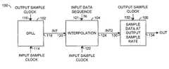
- the circuit 10includes a low pass filter (LPF) circuit 12 and a sample clock reduction circuit 14 .
- the LPF 102may be an anti-aliasing low pass filter.
- an input data sequenceis applied to the low pass filter 12 and the circuit 14 .
- the circuit 12has an input 20 that receives an input data sequence signal (IN), an input 22 that receives an input sample clock signal FS and an output 24 that presents a signal INT.
- the circuit 12has an input 26 that receives the signal INT, an input 28 that receives an output sample clock signal and an output 30 that presents an output data sequence (e.g., OUT).
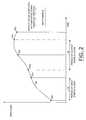
- FIG. 2a diagram is shown illustrating a time response with fixed down sampling.
- a continuous time waveform 50is sampled periodically at a number of input sample points 52 a - 52 d by the input and output sample clock.
- the input sample points 52 a - 52 dare interpolated to calculate output sample points 54 a - 54 b sampled at a longer period.
- a typical fixed rate down sampling processcomputes the output samples shown in FIG. 2 .
- the input sampling clock periodis represented by arrow 56 .
- the output sampling clock periodis represented by arrow 58 .
- the resampled signalis estimated at a multiple of the estimated output sample period.
- the output sample periodis estimated as a fixed ratio of the input sample period.
- the fixed down sampling processdoes not track a change in the relationship between the input clock period and the output clock period. If the input sample period decreases, the estimated output clock period also decreases. Similarly, if the input clock period increases, the estimated output clock period also increases. Therefore, in a fixed down-sampling process, the estimated period of the output clock varies in proportion to the input clock period. As the period of the input clock changes, the time at which the resampled signal amplitude is estimated also changes, causing an amplitude error in the estimated resampled signal.
- FIG. 3shows an example of a reduction in the input sample period 56 ′ with no change in the output sample clock period 58 .
- the estimated output samples 54 a and 54 bare computed at incorrect times 60 a and 60 b .
- the actual output sampling instants 62 a and 62 bare computed as a function of the input sample period 56 ′. Since the input sample period 56 ′ has been reduced as compared with FIG. 1 , the estimated output sample period has also been reduced, causing errors 64 a and 64 b in the estimated amplitude of the signal 50 at the output clock rate. Instead of computing the amplitude of the signal 50 at the output sample points 54 a and 54 b , the sample points 62 a and 62 b are calculated at time 60 a and 60 b , respectively.
- the present inventionconcerns an apparatus generally comprising a first circuit, a second circuit and a third circuit.
- the first circuitmay be configured to generate a phase signal by dividing each cycle of an output clock into a plurality of phase values.
- the second circuitmay be configured to generate an intermediate data signal by interpolating an input data signal sampled with an input clock in response to the phase signal and the output clock.
- the third circuitconfigured to generate an output data signal by sampling the intermediate data signal with the output clock.
- variable data rate conversionmay (i) automatically apply filter coefficients to maintain spectral purity of the digitized waveform as the input data rate changes with respect to the output data rate, and/or (ii) reduce low frequency distortion (e.g., wow) and frequency fluctuations (e.g., flutter) in the output signal after data rate conversion, such as when an audio signal sampled by a phase lock loop (PLL) is presented by a crystal clock operating at one of several industry standard clock rates.
- PLLphase lock loop
- FIG. 1is a block diagram illustrating a conventional fixed down sampling process
- FIG. 2is a diagram illustrating an example of time response with fixed down sampling of the circuit of FIG. 1 ;
- FIG. 3is a diagram illustrating an example of time response amplitude error with fixed down sampling of the circuit of FIG. 1 ;
- FIG. 4is a diagram illustrating an input sampling and an output sampling of an example signal
- FIG. 5is a block diagram of an example circuit implementing an adaptive data rate conversion in accordance with a preferred embodiment of the present invention
- FIG. 6is a block diagram of an example implementation of a digital phase locked loop circuit
- FIG. 7is a diagram illustrating an example transfer function implemented within a phase detector circuit
- FIG. 8is a block diagram of an example circuit implementing a phase detector circuit
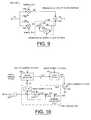
- FIG. 9is a block diagram of an example architecture for a loop filter circuit
- FIG. 10is a block diagram of an example architecture for a numerically controlled oscillator circuit and a delay circuit
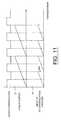
- FIG. 11is a timing diagram of example waveforms for an oscillator signal and an intermediate signal relative to an output sample clock.
- FIG. 12is a diagram illustrating a linear interpolation.
- the present inventionintroduces a fixed down-sampling process.
- An amplitude errormay be created by a change in a sample clock rate of an input signal while the sample clock rate of an output signal remains fixed.
- the present inventionmay implement an adaptive data rate conversion (ADRC) that computes the proper output sample as the input sample clock rate changes.
- ADRCadaptive data rate conversion
- FIG. 4a diagram illustrating an input sampling and an output sampling of an example signal 90 is shown.
- the present inventionmay provide a method and/or architecture to accurately interpolate the sampled signal 90 , while an input sample period 92 changes in relationship to a fixed output sample period 94 . Therefore, the estimated resampled signal may be computed at or proximate the correct time.
- the signal 90may be sampled per the input sample clock to generate input sample points 96 a - 96 d .
- Interpolated output sample points 98 a and 98 bmay then be calculated in alignment with the output sampling clock period 94 regardless of a phase relationship and/or frequency relationship between the input sampling clock period 92 and the output sampling clock period 94 .
- the estimated output sample periodmay remain fixed.
- the process described by the present inventioncontinuously computes the relationship between the variable input clock period 92 and the fixed output clock period 94 .
- an estimated amplitude of the signal 90 measured at the output clock rateis generally computed at approximately the correct instant of time.
- the resampled signal 90may be computed at the correct time as shown by the example in FIG. 4 . Even as the input sample clock period 92 increases, the present invention computes the resampled signal at a multiple of the output clock period 94 . The present invention accurately estimates the resampled signal by tracking the relationship between the input and output clock rates and interpolating the samples of the signal.
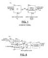
- the circuit 100generally comprises a block (or circuit) 102 , a block (or circuit) 104 and a block (or circuit) 106 .
- the circuit 102may have an input 110 that may receive an output sample clock signal (e.g., OSC), an input 114 that may receive an input sample clock signal (e.g., ISC) and an output 116 that may present an intermediate signal (e.g., INT).
- OSCoutput sample clock signal
- ISCinput sample clock signal
- INTan intermediate signal
- the circuit 104may have an input 120 that may receive the signal INT, an input 121 that may receive an input data sequence signal (e.g., IN), an input 122 that may receive the input sample clock ISC and an output 124 that may present another intermediate signal (e.g., INT 2 ).
- the circuit 106may have an input 130 that may receive the signal INT 2 , an input 132 that may receive the output sample clock signal OSC and an output 134 that may present an output data sequence signal (e.g., OUT).
- the circuit 102may be implemented as a digital phase lock loop (DPLL) circuit.
- the DPLL circuit 102generally synchronizes the variable-period input sample clock ISC to the fixed-period output sample clock OSC.
- the DPLL circuit 102may compute a phase relationship between the output sample clock OSC and the intermediate signal INT.
- the interpolation circuit 104From samples of the input sample clock ISC, the output sample clock OSC and the phase relationship, the interpolation circuit 104 generally estimates interpolated output samples at the output sample rate.
- the interpolated samplesmay be presented in the second intermediate signal INT 2 to the circuit 106 .
- the sample circuit 106samples the data at the output sample clock OSC rate.
- the circuit 106may be implemented as a register or register array to store the samples.
- the DPLL circuit 102generally comprises a block (or circuit) 142 , a block (or circuit) 144 , a block (or circuit) 146 , a block (or circuit) 148 , a block (or circuit) 150 , and a block (or circuit) 152 .
- the circuit 142may be implemented as a phase detector circuit.
- the circuit 144may be implemented as a loop filter circuit.
- the circuit 146may be implemented as a numerically controlled oscillator circuit (NCO).
- the circuit 148may be implemented as a delay unit such as a register or register array.
- the circuit 150may be implemented as a shifter or divider circuit.
- the circuit 152may be implemented as another shifter or divider circuit.
- the DPLL circuit 102generally passes a phase from the NCO circuit 146 to the interpolation process performed by the interpolation circuit 104 .
- the phase detector circuit 142 and the loop filter circuit 144may operate at a fraction of the input sample clock rate.
- the NCO circuit 146may operate at the input sample clock rate.
- the phase detector circuit 142generally measures a phase error between an oscillating signal generated by the NCO circuit 146 and the fixed period output sample clock OSC. To measure the phase error, the phase detector circuit 142 may measure a value of the signal A at positive edges of the divided output sample clock OSC.
- the phase detector circuit 142may receive the input sample clock ISC, a divided version of the output sample clock (e.g., OSC/V, where V may be an integer such as 2) and a signal (e.g., A).
- the phase detector circuit 142may generate a signal (e.g., B).
- the signal Bmay be an error signal conveying a phase error between the divided output sample clock OSC and the signal A.
- the signal Amay transfer a periodic sequence of phase values.
- Each phase valuemay be represented as a multi-bit (e.g., 17-bit) number.
- the phase values in the oscillator signal Amay be implemented as unsigned numbers.
- the phase error values in the phase error signal Bmay be implemented as signed numbers.
- the input sample clock ISCmay provide control of when the phase error values are changed or updated in the phase error signal B.
- the loop filter circuit 144generally controls (i) a response time of a loop within the DPLL circuit 102 and (ii) a steady-state variance of the oscillating signal generated by the NCO circuit 146 .
- the loop filter circuit 144may receive the signal B and a divided version of the input sample clock (e.g., ISC/W, where W may be an integer such as 4).
- the loop filter circuit 144may filter the signal B to generate a filtered signal (e.g., C).
- the signal Cmay also implement a phase error signal transferring a period sequence of filtered phase error values. Each filtered phase error value may be represented as a multi-bit (e.g., 30-bit signed) number.
- the divided input sample clock ISC/4may provide control of when the filtered phase error values are changed or updated in the filtered phase error signal C.
- the delay circuit 148may delay the filtered phase error signal C to generate a delayed phase error signal (e.g., D).
- a duration of the delaymay be determined by the divided input sample clock ISC/4.
- the delayed error signal Dmay be represented as a period sequence of multi-bit (e.g., 30-bit signed) phase error values.
- the NCO circuit 146may be implemented as an accumulator that computes a phase relationship between the input sample clock ISC and the output sample clock OSC.
- the NCO circuit 146may generate an oscillating signal (e.g., E) based upon the delayed phase error signal D and the input sample clock ISC.
- the oscillator signal Emay be represented as a sequence of amplitude values. Each amplitude value may be implemented as a multi-bit (e.g., 32-bit unsigned) number. A change rate of the amplitude values may be controlled by the input sample clock ISC.
- the oscillator signal Emay produce a period signal having a variable cycle period or time. Changes to the variable cycle period may track changes in the period 92 of the input sample clock ISC.
- the oscillator signal Emay be implemented a sawtooth shaped waveform. Other waveforms may be implemented to meet the criteria of a particular application.
- the shifter circuit 150may shift the amplitude values in the oscillator signal E several bits (e.g., 15 bits) to generate the signal A.
- the signal Amay therefore be a reduced amplitude oscillator signal.
- Discrete values within the signal Amay be represented by as multi-bit (e.g., 17-bit unsigned) numbers.
- the shifter circuit 152may shift the amplitude values in the oscillator signal E by a few bits (e.g., 1 bit) to generate the intermediate signal INT. Therefore, the intermediate signal INT may implement a phase signal.
- the phase signal INTgenerally carries a periodic sequence of phase values. Each phase value may be implemented as a multi-bit (e.g., 31-bit unsigned) number. A change rate of the phase values may be governed by the input sample clock ISC.
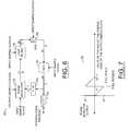
- the transfer function 160generally relates an amplitude of the phase error signal B (shown along the y-axis) to the oscillator signal E (shown along the x-axis). If the amplitude value of the oscillator signal E is less than or equal to half a full scale value (where the maximum full scale value may be 2 ⁇ 32 ⁇ 1), the transfer function 160 may generate the phase error signal B with an amplitude equal to a negative of the amplitude of the reduced oscillator signal A.
- the y-axisranges from 2 ⁇ 16 ⁇ 1 to ⁇ 2 ⁇ 16 per the 17-bit signal B. If the value of the oscillator output signal A is greater than half of the full scale value, the transfer function 160 may generate the phase error signal B with an amplitude equal to the full scale value minus the amplitude value of the reduced oscillator signal A.
- the phase detector circuit 142generally uses a reduced output sample clock (e.g., OSC/V, where V may be an integer such as 2) so that there may be a sufficient number of input sample clock ISC periods 92 to perform a proper synchronization of the output sample clock OSC into the input sample clock ISC domain. Therefore, the NCO circuit 146 may operate at the input sample clock ISC rate and the oscillator signal E may roll over at the reduced output sample clock rate OSC/2.
- OSC/Vreduced output sample clock
- the phase detector circuit 142generally comprises a block (or circuit) 162 , a block (or circuit) 164 , a block (or circuit) 168 , a block (or circuit) 170 , a block (or circuit) 172 and a block (or circuit) 174 .
- the circuit 162may be implemented as a divider circuit.
- the divider circuit 172may divide the output sample clock OSC by a predetermined integer (e.g., 2) to produce a clock (e.g., J).
- the circuit 164may be implemented as a synchronizer circuit.
- the synchronizer circuit 164may synchronize the clock J with the input sample clock ISC to generate another clock (e.g., K).
- the circuit 168may be implemented as a multiplexer circuit.
- the multiplexer circuit 168may receive the clock K as an address to route one of multiple inputs to an output.
- a signal (e.g., L) at the output of the multiplexer circuit 168may be feed back to a first input (e.g., input 0) of the multiplexer circuit 168 .
- a second input (e.g., input 1) of the multiplexer circuit 168may receive another signal (e.g., M).
- the circuit 170may be implemented as a pipeline delay circuit.
- the pipeline delay circuit 170may generate the signal M by delaying the reduced oscillator signal A.
- the pipeline delay circuit 170may be used to match a delay of the output sample clock OSC through the divider circuit 162 and the synchronization circuit 164 .
- the pipeline delay circuit 170may receive the input sample clock ISC for control of the delay time.
- the circuit 172may be a register implementing a delay unit.
- the register 172may store the signal L on rising (or falling) edges of the input sample clock ISC.
- An output of the register 172may present the stored value as another signal (e.g., N).
- the circuit 174may be implemented as a transfer circuit.
- the transfer circuit 174may implement a transfer function such as the transfer function 160 shown in FIG. 7 . Other transfer functions may be implemented to meet the criteria of a particular application.
- the transfer circuit 174may operate on the signal N to produce the phase error signal B.
- a loop filter model 180is generally implemented with a proportional path 182 and an integral path 184 .
- the proportional path 182generally approaches a zero value and an integrator 186 in the integral path 184 may reach a nominal frequency of the oscillator signal E and a frequency of the output sample clock OSC.
- the loop filter model 180generally comprises a summation 190 , a multiplier 192 , a multiplier 194 and the integrator 186 .
- the summation 190may add the values in the proportional path 182 and the integral path 184 .
- the multiplier 192may provide a gain for the proportional path.
- a predetermined valuee.g., ADRDG_R11
- the multiplier 194may provide a gain for the integral path 184 .
- a predetermined value(e.g., ADRIG_R11) may be received by the multiplier 194 to set the integral path gain.
- the integrator 186generally comprises a multiplier 196 and a delay unit 200 .
- the delay unit 200may receive the divided input sample clock ISC/4 to control the delay time.
- a model 210 for the NCO circuit 146 and the delay circuit 150generally comprises a summation 212 , a summation 214 , a delay unit 216 and a shift operation 218 .
- a nominal frequency step signalgenerally controls a nominal frequency of the NCO circuit 146 at the summation 212 .
- the summation 214 and delay unit 216may be arranged to generate the oscillator signal E.
- the shift operation 218may model the operation of the shift circuit 150 .
- the loop filter circuit 144 and delay circuit 148may update the phase and frequency of the oscillator signal E. Once the DPLL circuit 102 locks, the phase and frequency of the oscillator signal E generally tracks the phase and frequency of the output sample clock OSC, respectively.
- the oscillator signal Egenerally rolls over (e.g., rapidly transitions from a high value to a low value) at half the output sample clock OSC rate, a portion (e.g., the lower 31 bits) of the oscillator signal E may be applied to the interpolation circuit 104 .
- the second most significant bit (MSB) of the oscillator signal Emay roll over at twice the roll over rate of the oscillator signal E. Therefore, the second MSB of the oscillator signal E may be used as the MSB of the signal INT provided to the interpolation process.
- FIG. 11a timing diagram of example waveforms for the oscillator signal E and the intermediate signal INT relative to the output sample clock OSC are shown.
- the output sample clock OSC and the intermediate signal INTgenerally show a one cycle-to-one cycle relationship.
- the intermediate signal INT and the oscillator signal Egenerally show a two cycle-to-one cycle relationship.
- the intermediate signal INTmay begin at a low value (e.g., zero) at each rising edge of the output sample clock OSC.
- the phase value of the intermediate signal INTmay ramp up in a linear fashion to a high (e.g., approximately half full scale) value by the end of the present cycle.
- a roll over 220 of the intermediate signal INTmay take place proximate each subsequent rising edge of the output sample clock OSC.
- the interpolation process performed by the interpolation circuit 104generally estimates the values of the output samples that change on the positive edge of the output sample clock OSC.
- a formula to calculate the output samplesmay be provided in equation 1 as follows:
- y ⁇ ( n )x ⁇ ( n - 1 ) + [ x ⁇ ( n ) - x ⁇ ( n - 1 ) ] ⁇ ( Full_Scale - NCO ⁇ ( n - 1 ) NCO ⁇ ( n ) + Full_Scale - NCO ⁇ ( n - 1 ) Eq . ⁇ ( 1 )
- the variable x(n)may represent an input sample value sampled at the input sample clock ISC rate.
- the variable y(n)may represent a new sample computed by the interpolation process.
- the variable NCO(n)may represent a phase value within the intermediate signal INT taken at an input sample clock ISC edge n.
- the constant Full_Scalemay represent a maximum value of the intermediate signal INT.
- the variable NCOmay divide each cycle of the output sample clock OSC into multiple time slices. Each time slice may be identified by the phase values presented by the variable NCO (e.g., the phase values in the intermediate signal INT). Therefore, any particular NCO value may indicate an instantaneous phase position in a clock cycle.
- the phase values or positionsmay be used by the interpolation process in determining when to calculate the sample values for the second intermediate signal INT 2 .
- a continuous waveform or the input data sequence INmay be sampled at the input sample clock ISC period 92 to generate a sequence of sample values 222 a - 222 e .
- Interpolated samples 224 a - 224 bmay be computed as a function of the input samples 222 measured just before and just after a particular edge of the output sample clock OSC as identified by a roll over in the intermediate signal INT. Each roll over generally indicates a time of a positive edge in the output sample clock OSC.
- the sample circuit 106may sample the estimated value at the fixed output sample clock OSC period 94 to form the output data sequence OUT.
- the adaptive data rate conversion showngenerally computes the interpolated samples 224 by linearly interpolating between two consecutive samples 222 .
- the fractional term generated by in right-hand side of equation 1may determine a phase or time percentage between the consecutive samples 222 to calculate the interpolated samples 224 .
- the interpolationmay occur close to the prior sample n ⁇ 1.
- the interpolationmay occur close to the current sample n. Since the intermediate signal INT is quantized in time, the interpolations may occur proximate to simultaneous with the positive edges of the output sample clock OSC.
- the actual values 226 a and 226 b of the input data sequence IN at the interpolation pointsmay be slightly different (e.g., larger or smaller) than the interpolated values 224 a and 224 b , respectively. Therefore, the adaptive data rate conversion process and apparatus of the present invention may apply higher-order interpolation filters.
- the higher-order interpolation filtersmay reduce the error between the interpolated samples 224 and the actual values 226 of the input data sequence IN at the output sample clock OSC edges.
- an interpolation methodmay consider two input samples before and two input samples after a particular interpolation time in calculating the interpolated value.
- Other applicationsmay include techniques to reduce data rate jitter by using changes in the input data rate to one or more filter coefficients to provide a stable data rate on the filter output that would be resampled at a mean frequency of the time varying input data rate.
- the various signals of the present inventionare generally “on” (e.g., a digital HIGH, or 1) or “off” (e.g., a digital LOW, or 0).
- the particular polarities of the on (e.g., asserted) and off (e.g., de-asserted) states of the signalsmay be adjusted (e.g., reversed) accordingly to meet the design criteria of a particular implementation.
- invertersmay be added to change a particular polarity of the signals.
- the term “simultaneously”is meant to describe events that share some common time period but the term is not meant to be limited to events that begin at the same point in time, end at the same point in time, or have the same duration.
Landscapes
- Engineering & Computer Science (AREA)
- Computer Networks & Wireless Communication (AREA)
- Signal Processing (AREA)
- Synchronisation In Digital Transmission Systems (AREA)
- Stabilization Of Oscillater, Synchronisation, Frequency Synthesizers (AREA)
Abstract
Description
The variable x(n) may represent an input sample value sampled at the input sample clock ISC rate. The variable y(n) may represent a new sample computed by the interpolation process. The variable NCO(n) may represent a phase value within the intermediate signal INT taken at an input sample clock ISC edge n. The constant Full_Scale may represent a maximum value of the intermediate signal INT.
Claims (18)
Priority Applications (1)
| Application Number | Priority Date | Filing Date | Title |
|---|---|---|---|
| US10/354,456US7764758B2 (en) | 2003-01-30 | 2003-01-30 | Apparatus and/or method for variable data rate conversion |
Applications Claiming Priority (1)
| Application Number | Priority Date | Filing Date | Title |
|---|---|---|---|
| US10/354,456US7764758B2 (en) | 2003-01-30 | 2003-01-30 | Apparatus and/or method for variable data rate conversion |
Publications (2)
| Publication Number | Publication Date |
|---|---|
| US20040151267A1 US20040151267A1 (en) | 2004-08-05 |
| US7764758B2true US7764758B2 (en) | 2010-07-27 |
Family
ID=32770373
Family Applications (1)
| Application Number | Title | Priority Date | Filing Date |
|---|---|---|---|
| US10/354,456Expired - Fee RelatedUS7764758B2 (en) | 2003-01-30 | 2003-01-30 | Apparatus and/or method for variable data rate conversion |
Country Status (1)
| Country | Link |
|---|---|
| US (1) | US7764758B2 (en) |
Cited By (2)
| Publication number | Priority date | Publication date | Assignee | Title |
|---|---|---|---|---|
| US20080033726A1 (en)* | 2004-12-27 | 2008-02-07 | P Softhouse Co., Ltd | Audio Waveform Processing Device, Method, And Program |
| US20140101218A1 (en)* | 2006-02-16 | 2014-04-10 | Sigmatel, Inc. | Decimation filter |
Families Citing this family (3)
| Publication number | Priority date | Publication date | Assignee | Title |
|---|---|---|---|---|
| US7764758B2 (en)* | 2003-01-30 | 2010-07-27 | Lsi Corporation | Apparatus and/or method for variable data rate conversion |
| US8000423B2 (en)* | 2005-10-07 | 2011-08-16 | Zoran Corporation | Adaptive sample rate converter |
| JP2008203367A (en)* | 2007-02-16 | 2008-09-04 | Sharp Corp | Developer storage container and image forming apparatus |
Citations (39)
| Publication number | Priority date | Publication date | Assignee | Title |
|---|---|---|---|---|
| US3681756A (en)* | 1970-04-23 | 1972-08-01 | Industrial Research Prod Inc | System for frequency modification of speech and other audio signals |
| US4748578A (en)* | 1980-11-26 | 1988-05-31 | Willi Studer | Process and apparatus for translating the sampling rate of a sampling sequence |
| US4851909A (en)* | 1987-09-24 | 1989-07-25 | Robert Bosch Gmbh | Method and apparatus for maintaining audio/ video synchronism in a television signal read-out from a digital buffer memory by a reference signal |
| US4870661A (en)* | 1986-09-30 | 1989-09-26 | Kabushiki Kaisha Toshiba | Sample rate conversion system having interpolation function |
| US5126737A (en)* | 1990-04-16 | 1992-06-30 | Yamaha Corporation | Method for converting a digital signal into another digital signal having a different sampling frequency |
| US5175769A (en)* | 1991-07-23 | 1992-12-29 | Rolm Systems | Method for time-scale modification of signals |
| US5225787A (en)* | 1991-05-10 | 1993-07-06 | U.S. Philips Corporation | Sampling frequency converter including a sigma-delta modulator |
| US5228138A (en)* | 1991-01-23 | 1993-07-13 | Massachusetts Institute Of Technology | Synchronization of hardware oscillators in a mesh-connected parallel processor |
| US5398029A (en)* | 1992-12-21 | 1995-03-14 | Nippon Precision Circuits Inc. | Sampling rate converter |
| US5432511A (en)* | 1992-05-21 | 1995-07-11 | Sony United Kingdom, Ltd. | Sampling frequency conversion using interrupt control |
| US5481267A (en)* | 1993-01-07 | 1996-01-02 | Nippon Precision Circuits Inc. | Sampling rate converter |
| US5497152A (en)* | 1993-09-13 | 1996-03-05 | Analog Devices, Inc. | Digital-to-digital conversion using non-uniform sample rates |
| US5513209A (en)* | 1993-02-26 | 1996-04-30 | Holm; Gunnar | Resampling synchronizer of digitally sampled signals |
| US5559513A (en)* | 1993-08-06 | 1996-09-24 | Deutsche Thomson-Brandt Gmbh | Digital sampling rate converter |
| US5617088A (en)* | 1994-01-26 | 1997-04-01 | Sony Corporation | Sampling frequency converting device and memory address control device |
| US5748397A (en)* | 1994-06-24 | 1998-05-05 | Sony Corporation | Audio signal processing apparatus and recording and/or reproducing apparatus for a tape-shaped recording medium |
| US5764113A (en)* | 1997-01-10 | 1998-06-09 | Harris Corporation | Re-sampling circuit and modulator using same |
| US5786778A (en)* | 1995-10-05 | 1998-07-28 | Analog Devices, Inc. | Variable sample-rate DAC/ADC/converter system |
| US5920842A (en)* | 1994-10-12 | 1999-07-06 | Pixel Instruments | Signal synchronization |
| US5925093A (en)* | 1996-10-15 | 1999-07-20 | Sony Corporation | Sampling frequency converting apparatus |
| US5982208A (en)* | 1997-07-14 | 1999-11-09 | Oki Electric Industry Co., Ltd. | Clock multiplier having two feedback loops |
| US6014682A (en)* | 1997-05-30 | 2000-01-11 | International Business Machines Corporation | Methods and apparatus for variable-rate down-sampling filters for discrete-time sampled systems using a fixed sampling rate |
| US6067319A (en)* | 1996-09-04 | 2000-05-23 | Integrated Device Technology, Inc. | Method for equalization of a quadrature amplitude modulated signal |
| US6137349A (en)* | 1997-07-02 | 2000-10-24 | Micronas Intermetall Gmbh | Filter combination for sampling rate conversion |
| US6147632A (en)* | 1997-03-12 | 2000-11-14 | Nec Corporation | Sampling frequency conversion apparatus and fractional frequency dividing apparatus for sampling frequency conversion |
| US6154497A (en)* | 1996-12-19 | 2000-11-28 | Texas Instruments Incorporated | Method and system for analog to digital conversion |
| US6208671B1 (en)* | 1998-01-20 | 2001-03-27 | Cirrus Logic, Inc. | Asynchronous sample rate converter |
| US20010033188A1 (en)* | 2000-03-14 | 2001-10-25 | Edward Aung | Clock data recovery circuitry associated with programmable logic device circuitry |
| US20010037351A1 (en)* | 2000-03-27 | 2001-11-01 | Richard Hellberg | Sample rate conversion method and apparatus |
| US20020110213A1 (en)* | 2001-02-13 | 2002-08-15 | Sigma Tel, Inc. | Method and apparatus for providing data for sample rate conversion |
| US6563448B1 (en)* | 2002-04-29 | 2003-05-13 | Texas Instruments Incorporated | Flexible sample rate converter for multimedia digital-to-analog conversion in a wireless telephone |
| US6573940B1 (en)* | 1999-09-02 | 2003-06-03 | Techwell, Inc | Sample rate converters for video signals |
| US20030117925A1 (en)* | 2001-12-26 | 2003-06-26 | Junichiro Tonami | Reproducing apparatus |
| US6590948B1 (en)* | 2000-03-17 | 2003-07-08 | Raytheon Company | Parallel asynchronous sample rate reducer |
| US6665338B1 (en)* | 2000-01-05 | 2003-12-16 | Motorola, Inc. | Circuitry for converting a sampled digital signal to a naturally sampled digital signal and method therefor |
| US20040151267A1 (en)* | 2003-01-30 | 2004-08-05 | Lsi Logic Corporation | Apparatus and/or method for variable data rate conversion |
| US6778600B1 (en)* | 2000-05-12 | 2004-08-17 | Ati International Srl | Method of filtering and apparatus therefore |
| US6778621B1 (en)* | 2000-10-18 | 2004-08-17 | Lockheed Martin Corporation | Precision resampling system |
| US20050130656A1 (en)* | 2002-03-13 | 2005-06-16 | Hongyuan Chen | Method and apparatus for performing handover in a bluetooth radiocommunication system |
- 2003
- 2003-01-30USUS10/354,456patent/US7764758B2/ennot_activeExpired - Fee Related
Patent Citations (47)
| Publication number | Priority date | Publication date | Assignee | Title |
|---|---|---|---|---|
| US3681756A (en)* | 1970-04-23 | 1972-08-01 | Industrial Research Prod Inc | System for frequency modification of speech and other audio signals |
| US4748578A (en)* | 1980-11-26 | 1988-05-31 | Willi Studer | Process and apparatus for translating the sampling rate of a sampling sequence |
| US4870661A (en)* | 1986-09-30 | 1989-09-26 | Kabushiki Kaisha Toshiba | Sample rate conversion system having interpolation function |
| US4851909A (en)* | 1987-09-24 | 1989-07-25 | Robert Bosch Gmbh | Method and apparatus for maintaining audio/ video synchronism in a television signal read-out from a digital buffer memory by a reference signal |
| US5126737A (en)* | 1990-04-16 | 1992-06-30 | Yamaha Corporation | Method for converting a digital signal into another digital signal having a different sampling frequency |
| US5228138A (en)* | 1991-01-23 | 1993-07-13 | Massachusetts Institute Of Technology | Synchronization of hardware oscillators in a mesh-connected parallel processor |
| US5225787A (en)* | 1991-05-10 | 1993-07-06 | U.S. Philips Corporation | Sampling frequency converter including a sigma-delta modulator |
| US5175769A (en)* | 1991-07-23 | 1992-12-29 | Rolm Systems | Method for time-scale modification of signals |
| US5432511A (en)* | 1992-05-21 | 1995-07-11 | Sony United Kingdom, Ltd. | Sampling frequency conversion using interrupt control |
| US5398029A (en)* | 1992-12-21 | 1995-03-14 | Nippon Precision Circuits Inc. | Sampling rate converter |
| US5481267A (en)* | 1993-01-07 | 1996-01-02 | Nippon Precision Circuits Inc. | Sampling rate converter |
| US5513209A (en)* | 1993-02-26 | 1996-04-30 | Holm; Gunnar | Resampling synchronizer of digitally sampled signals |
| US5559513A (en)* | 1993-08-06 | 1996-09-24 | Deutsche Thomson-Brandt Gmbh | Digital sampling rate converter |
| US5497152A (en)* | 1993-09-13 | 1996-03-05 | Analog Devices, Inc. | Digital-to-digital conversion using non-uniform sample rates |
| US5617088A (en)* | 1994-01-26 | 1997-04-01 | Sony Corporation | Sampling frequency converting device and memory address control device |
| US5748120A (en)* | 1994-01-26 | 1998-05-05 | Sony Corporation | Sampling frequency converting device and memory address control device |
| US5996044A (en)* | 1994-01-26 | 1999-11-30 | Sony Corporation | Sampling frequency converting device and memory address control device |
| US5835032A (en)* | 1994-01-26 | 1998-11-10 | Sony Corporation | Sampling frequency converting device and memory address control device |
| US5748397A (en)* | 1994-06-24 | 1998-05-05 | Sony Corporation | Audio signal processing apparatus and recording and/or reproducing apparatus for a tape-shaped recording medium |
| US5920842A (en)* | 1994-10-12 | 1999-07-06 | Pixel Instruments | Signal synchronization |
| US6421636B1 (en)* | 1994-10-12 | 2002-07-16 | Pixel Instruments | Frequency converter system |
| US6973431B2 (en)* | 1994-10-12 | 2005-12-06 | Pixel Instruments Corp. | Memory delay compensator |
| US6098046A (en)* | 1994-10-12 | 2000-08-01 | Pixel Instruments | Frequency converter system |
| US5786778A (en)* | 1995-10-05 | 1998-07-28 | Analog Devices, Inc. | Variable sample-rate DAC/ADC/converter system |
| US6067319A (en)* | 1996-09-04 | 2000-05-23 | Integrated Device Technology, Inc. | Method for equalization of a quadrature amplitude modulated signal |
| US5925093A (en)* | 1996-10-15 | 1999-07-20 | Sony Corporation | Sampling frequency converting apparatus |
| US6154497A (en)* | 1996-12-19 | 2000-11-28 | Texas Instruments Incorporated | Method and system for analog to digital conversion |
| US5764113A (en)* | 1997-01-10 | 1998-06-09 | Harris Corporation | Re-sampling circuit and modulator using same |
| US6147632A (en)* | 1997-03-12 | 2000-11-14 | Nec Corporation | Sampling frequency conversion apparatus and fractional frequency dividing apparatus for sampling frequency conversion |
| US6249235B1 (en)* | 1997-03-12 | 2001-06-19 | Nec Corporation | Sampling frequency conversion apparatus and fractional frequency dividing apparatus for sampling frequency |
| US6014682A (en)* | 1997-05-30 | 2000-01-11 | International Business Machines Corporation | Methods and apparatus for variable-rate down-sampling filters for discrete-time sampled systems using a fixed sampling rate |
| US6137349A (en)* | 1997-07-02 | 2000-10-24 | Micronas Intermetall Gmbh | Filter combination for sampling rate conversion |
| US5982208A (en)* | 1997-07-14 | 1999-11-09 | Oki Electric Industry Co., Ltd. | Clock multiplier having two feedback loops |
| US6208671B1 (en)* | 1998-01-20 | 2001-03-27 | Cirrus Logic, Inc. | Asynchronous sample rate converter |
| US6573940B1 (en)* | 1999-09-02 | 2003-06-03 | Techwell, Inc | Sample rate converters for video signals |
| US6665338B1 (en)* | 2000-01-05 | 2003-12-16 | Motorola, Inc. | Circuitry for converting a sampled digital signal to a naturally sampled digital signal and method therefor |
| US20010033188A1 (en)* | 2000-03-14 | 2001-10-25 | Edward Aung | Clock data recovery circuitry associated with programmable logic device circuitry |
| US6590948B1 (en)* | 2000-03-17 | 2003-07-08 | Raytheon Company | Parallel asynchronous sample rate reducer |
| US6462682B2 (en)* | 2000-03-27 | 2002-10-08 | Telefonaktiebolaget Lm Ericsson (Publ) | Sample rate conversion method and apparatus |
| US20010037351A1 (en)* | 2000-03-27 | 2001-11-01 | Richard Hellberg | Sample rate conversion method and apparatus |
| US6778600B1 (en)* | 2000-05-12 | 2004-08-17 | Ati International Srl | Method of filtering and apparatus therefore |
| US6778621B1 (en)* | 2000-10-18 | 2004-08-17 | Lockheed Martin Corporation | Precision resampling system |
| US20020110213A1 (en)* | 2001-02-13 | 2002-08-15 | Sigma Tel, Inc. | Method and apparatus for providing data for sample rate conversion |
| US20030117925A1 (en)* | 2001-12-26 | 2003-06-26 | Junichiro Tonami | Reproducing apparatus |
| US20050130656A1 (en)* | 2002-03-13 | 2005-06-16 | Hongyuan Chen | Method and apparatus for performing handover in a bluetooth radiocommunication system |
| US6563448B1 (en)* | 2002-04-29 | 2003-05-13 | Texas Instruments Incorporated | Flexible sample rate converter for multimedia digital-to-analog conversion in a wireless telephone |
| US20040151267A1 (en)* | 2003-01-30 | 2004-08-05 | Lsi Logic Corporation | Apparatus and/or method for variable data rate conversion |
Cited By (4)
| Publication number | Priority date | Publication date | Assignee | Title |
|---|---|---|---|---|
| US20080033726A1 (en)* | 2004-12-27 | 2008-02-07 | P Softhouse Co., Ltd | Audio Waveform Processing Device, Method, And Program |
| US8296143B2 (en)* | 2004-12-27 | 2012-10-23 | P Softhouse Co., Ltd. | Audio signal processing apparatus, audio signal processing method, and program for having the method executed by computer |
| US20140101218A1 (en)* | 2006-02-16 | 2014-04-10 | Sigmatel, Inc. | Decimation filter |
| US9231562B2 (en)* | 2006-02-16 | 2016-01-05 | Sigmatel, Inc. | Decimation filter |
Also Published As
| Publication number | Publication date |
|---|---|
| US20040151267A1 (en) | 2004-08-05 |
Similar Documents
| Publication | Publication Date | Title |
|---|---|---|
| US5638010A (en) | Digitally controlled oscillator for a phase-locked loop providing a residue signal for use in continuously variable interpolation and decimation filters | |
| US6324235B1 (en) | Asynchronous sample rate tracker | |
| EP0599817B1 (en) | Sampling frequency conversion method and apparatus | |
| US6943714B2 (en) | Method and apparatus of obtaining power computation parameters | |
| US6005901A (en) | Arrangement for asynchronous decimation using a frequency ratio estimator and method thereof | |
| JP2986745B2 (en) | Composite phase filter, timing error compensating apparatus and method using the same | |
| US6518894B2 (en) | Device and method for sampling rate conversion | |
| JP3858160B2 (en) | Timing interpolator in a digital demodulator. | |
| US7408485B1 (en) | Asynchronous sampling rate converter and method for audio DAC | |
| US9379886B2 (en) | Sample rate converter and method of converting sample rate | |
| JP2009504107A (en) | Asynchronous sample rate converter | |
| US4905101A (en) | Time base corrector | |
| CN100521532C (en) | Data transmission controller and sampling frequency converter | |
| US7570727B2 (en) | Data transmission controller and sampling frequency converter | |
| US7764758B2 (en) | Apparatus and/or method for variable data rate conversion | |
| US6819732B1 (en) | Asynchronous sample rate estimation using reciprocal frequency error minimization | |
| US7342518B2 (en) | Digital rate converter | |
| US20030065463A1 (en) | Digital sample sequence conversion device | |
| US6559781B2 (en) | Device and method for sampling rate conversion | |
| US6778621B1 (en) | Precision resampling system | |
| US6941445B2 (en) | Resampling address generator | |
| US8942280B1 (en) | Method and apparatus for timing jitter measurement | |
| US6996168B2 (en) | Signal-processing circuit, and recording and playback apparatus employing the same | |
| US7425993B2 (en) | Video signal processing | |
| JP3420528B2 (en) | Sigma-delta D / A converter |
Legal Events
| Date | Code | Title | Description |
|---|---|---|---|
| AS | Assignment | Owner name:LSI LOGIC CORPORATION, CALIFORNIA Free format text:ASSIGNMENT OF ASSIGNORS INTEREST;ASSIGNORS:RABY, DEAN L.;CAULFIELD, ROBERT;REEL/FRAME:013722/0981;SIGNING DATES FROM 20030129 TO 20030130 Owner name:LSI LOGIC CORPORATION, CALIFORNIA Free format text:ASSIGNMENT OF ASSIGNORS INTEREST;ASSIGNORS:RABY, DEAN L.;CAULFIELD, ROBERT;SIGNING DATES FROM 20030129 TO 20030130;REEL/FRAME:013722/0981 | |
| AS | Assignment | Owner name:LSI CORPORATION, CALIFORNIA Free format text:MERGER;ASSIGNOR:LSI SUBSIDIARY CORP.;REEL/FRAME:020548/0977 Effective date:20070404 Owner name:LSI CORPORATION,CALIFORNIA Free format text:MERGER;ASSIGNOR:LSI SUBSIDIARY CORP.;REEL/FRAME:020548/0977 Effective date:20070404 | |
| FEPP | Fee payment procedure | Free format text:PAYOR NUMBER ASSIGNED (ORIGINAL EVENT CODE: ASPN); ENTITY STATUS OF PATENT OWNER: LARGE ENTITY | |
| FPAY | Fee payment | Year of fee payment:4 | |
| AS | Assignment | Owner name:DEUTSCHE BANK AG NEW YORK BRANCH, AS COLLATERAL AG Free format text:PATENT SECURITY AGREEMENT;ASSIGNORS:LSI CORPORATION;AGERE SYSTEMS LLC;REEL/FRAME:032856/0031 Effective date:20140506 | |
| AS | Assignment | Owner name:LSI CORPORATION, CALIFORNIA Free format text:CHANGE OF NAME;ASSIGNOR:LSI LOGIC CORPORATION;REEL/FRAME:033102/0270 Effective date:20070406 | |
| AS | Assignment | Owner name:AVAGO TECHNOLOGIES GENERAL IP (SINGAPORE) PTE. LTD Free format text:ASSIGNMENT OF ASSIGNORS INTEREST;ASSIGNOR:LSI CORPORATION;REEL/FRAME:035390/0388 Effective date:20140814 | |
| AS | Assignment | Owner name:LSI CORPORATION, CALIFORNIA Free format text:TERMINATION AND RELEASE OF SECURITY INTEREST IN PATENT RIGHTS (RELEASES RF 032856-0031);ASSIGNOR:DEUTSCHE BANK AG NEW YORK BRANCH, AS COLLATERAL AGENT;REEL/FRAME:037684/0039 Effective date:20160201 Owner name:AGERE SYSTEMS LLC, PENNSYLVANIA Free format text:TERMINATION AND RELEASE OF SECURITY INTEREST IN PATENT RIGHTS (RELEASES RF 032856-0031);ASSIGNOR:DEUTSCHE BANK AG NEW YORK BRANCH, AS COLLATERAL AGENT;REEL/FRAME:037684/0039 Effective date:20160201 | |
| AS | Assignment | Owner name:BANK OF AMERICA, N.A., AS COLLATERAL AGENT, NORTH CAROLINA Free format text:PATENT SECURITY AGREEMENT;ASSIGNOR:AVAGO TECHNOLOGIES GENERAL IP (SINGAPORE) PTE. LTD.;REEL/FRAME:037808/0001 Effective date:20160201 Owner name:BANK OF AMERICA, N.A., AS COLLATERAL AGENT, NORTH Free format text:PATENT SECURITY AGREEMENT;ASSIGNOR:AVAGO TECHNOLOGIES GENERAL IP (SINGAPORE) PTE. LTD.;REEL/FRAME:037808/0001 Effective date:20160201 | |
| AS | Assignment | Owner name:AVAGO TECHNOLOGIES GENERAL IP (SINGAPORE) PTE. LTD., SINGAPORE Free format text:TERMINATION AND RELEASE OF SECURITY INTEREST IN PATENTS;ASSIGNOR:BANK OF AMERICA, N.A., AS COLLATERAL AGENT;REEL/FRAME:041710/0001 Effective date:20170119 Owner name:AVAGO TECHNOLOGIES GENERAL IP (SINGAPORE) PTE. LTD Free format text:TERMINATION AND RELEASE OF SECURITY INTEREST IN PATENTS;ASSIGNOR:BANK OF AMERICA, N.A., AS COLLATERAL AGENT;REEL/FRAME:041710/0001 Effective date:20170119 | |
| FEPP | Fee payment procedure | Free format text:MAINTENANCE FEE REMINDER MAILED (ORIGINAL EVENT CODE: REM.) | |
| LAPS | Lapse for failure to pay maintenance fees | Free format text:PATENT EXPIRED FOR FAILURE TO PAY MAINTENANCE FEES (ORIGINAL EVENT CODE: EXP.); ENTITY STATUS OF PATENT OWNER: LARGE ENTITY | |
| STCH | Information on status: patent discontinuation | Free format text:PATENT EXPIRED DUE TO NONPAYMENT OF MAINTENANCE FEES UNDER 37 CFR 1.362 | |
| FP | Lapsed due to failure to pay maintenance fee | Effective date:20180727 |