US7764715B2 - Circuits and methods for data multiplexing - Google Patents
Circuits and methods for data multiplexingDownload PDFInfo
- Publication number
- US7764715B2 US7764715B2US10/623,028US62302803AUS7764715B2US 7764715 B2US7764715 B2US 7764715B2US 62302803 AUS62302803 AUS 62302803AUS 7764715 B2US7764715 B2US 7764715B2
- Authority
- US
- United States
- Prior art keywords
- clock
- delay
- circuit
- selector
- recited
- Prior art date
- Legal status (The legal status is an assumption and is not a legal conclusion. Google has not performed a legal analysis and makes no representation as to the accuracy of the status listed.)
- Active, expires
Links
- 238000000034methodMethods0.000titleclaimsabstractdescription33
- 230000007704transitionEffects0.000claimsdescription29
- 230000005540biological transmissionEffects0.000claimsdescription9
- 230000004044responseEffects0.000claimsdescription3
- 230000003111delayed effectEffects0.000abstractdescription10
- 238000004519manufacturing processMethods0.000abstractdescription6
- 230000035945sensitivityEffects0.000abstractdescription5
- 238000010586diagramMethods0.000description8
- 230000000630rising effectEffects0.000description7
- 230000001934delayEffects0.000description5
- 230000006870functionEffects0.000description5
- 230000008569processEffects0.000description5
- 230000008901benefitEffects0.000description4
- 230000004048modificationEffects0.000description2
- 238000012986modificationMethods0.000description2
- 230000006855networkingEffects0.000description2
- 230000009467reductionEffects0.000description2
- 230000002411adverseEffects0.000description1
- 239000003990capacitorSubstances0.000description1
- 238000006073displacement reactionMethods0.000description1
- 238000005516engineering processMethods0.000description1
- 230000007613environmental effectEffects0.000description1
- 230000008571general functionEffects0.000description1
- 239000000463materialSubstances0.000description1
- 230000007246mechanismEffects0.000description1
- 230000003287optical effectEffects0.000description1
- 230000001360synchronised effectEffects0.000description1
Images


Classifications
- H—ELECTRICITY
- H04—ELECTRIC COMMUNICATION TECHNIQUE
- H04J—MULTIPLEX COMMUNICATION
- H04J3/00—Time-division multiplex systems
- H04J3/02—Details
- H04J3/06—Synchronising arrangements
- H04J3/0635—Clock or time synchronisation in a network
- H04J3/0685—Clock or time synchronisation in a node; Intranode synchronisation
- H—ELECTRICITY
- H03—ELECTRONIC CIRCUITRY
- H03M—CODING; DECODING; CODE CONVERSION IN GENERAL
- H03M9/00—Parallel/series conversion or vice versa
- H—ELECTRICITY
- H04—ELECTRIC COMMUNICATION TECHNIQUE
- H04J—MULTIPLEX COMMUNICATION
- H04J3/00—Time-division multiplex systems
- H04J3/02—Details
- H04J3/04—Distributors combined with modulators or demodulators
- H04J3/047—Distributors with transistors or integrated circuits
- H—ELECTRICITY
- H04—ELECTRIC COMMUNICATION TECHNIQUE
- H04L—TRANSMISSION OF DIGITAL INFORMATION, e.g. TELEGRAPHIC COMMUNICATION
- H04L7/00—Arrangements for synchronising receiver with transmitter
- H04L7/0016—Arrangements for synchronising receiver with transmitter correction of synchronization errors
- H04L7/0033—Correction by delay
- H04L7/0037—Delay of clock signal
Definitions
- An embodiment of the present inventionrelates to the field of data transmission. More specifically, embodiments of the present invention relate to circuits and methods for data multiplexing.
- Modern computing, networking, communications, and other technologiescan require several streams of data to be transmitted across a single medium during the same time period. Multiplexing can effectuate such transmission, such as where multiple streams of data at a particular data rate are combined into a single stream of data at a higher data rate.
- a conventional two-to-one multiplexeris shown in Prior Art FIG. 1 .
- this multiplexertwo data streams, labeled D 1 and D 2 , are combined into a single data stream by a selector 101 .
- Selector 101is operated (e.g., controlled) by a clock signal, labeled CLK in the diagram.
- CLKclock signal
- the data signal D 1is passed to the output line, labeled D 3 .
- the signal CLKis high
- the data signal D 2is passed to the output line D 3 .
- the output linealternates between signals D 1 and D 2 , and the two input data signals are combined into a single data stream.
- the data signal D 1is provided by a first data latch 102 , whose output only changes after each rising edge of CLK.
- This timing relationshipis illustrated in timing diagram 103 , which shows that transitions 106 of the data signal D 1 occur in response to each rising edge of the CLK signal.
- D 1is stable during intervals when the CLK signal is low. This condition will be satisfied provided the clock-to-data delay (sometimes called “clock-to-Q” delay) of data latch 102 is less than half of the repetition period of the CLK signal.
- D 2is provided by a second data latch 104 , whose output only transitions in response to each falling edge of CLK, with the requirement that the transition be completed prior to the rising edge of CLK.
- a third latch 109delays D 2 by one half clock cycle, relative to D 1 .
- latchrefers to either a latch or a flip-flop.
- a flip-flopcan comprise two intercoupled, co-operational latches. As used herein, the term can refer to other logic circuit elements as well.
- Conventional multiplexer 101can be subject to an operating limitation at high frequencies. At high frequencies, the delay between the rising edge of CLK and a data transition on signal D 1 can become comparable to or greater than half of the clock period. If such a condition occurs, the falling edge 105 of CLK, which marks the beginning of the CLK low period, may arrive before the transition 106 in data signal D 1 is complete. Such a situation would violate the desired condition that D 1 be stable while the CLK signal is low. This violation can cause the output data D 3 to be corrupted.
- a similar problemcan occur on the rising edge of the clock signal if the delay of data latch 104 becomes correspondingly too long.
- the data signal D 2may still be in transition when clock signal CLK is high, which can also cause the output data D 3 to be corrupted.
- clock-to-Q delayThe delay from clock-to-data in a data latch, sometimes referred to as “clock-to-Q delay,” can depend on operational, pre-operational, environmental, and other variables.
- Such variablescan include, but are not limited to, variations in temperature, power supply voltage, manufacturing process, and fabrication. These variables can subject the performance of the multiplexer to variations that are not well controlled, and which can be undesirable. For example, a multiplexer that functions adequately at room temperature and nominal supply voltage may exhibit corrupt output data (e.g., fail to function adequately) at elevated temperature or reduced voltage.
- a circuit and method for data multiplexingare disclosed.
- a multiplexer according to one embodimentis capable of high-speed operation with acceptable timing margins and has reduced sensitivity to supply voltage, temperature and manufacturing variations.
- One embodiment of the present inventionrelates to a data multiplexer that has no significant speed limitation associated with the clock-to-data (e.g., clock to Q) delay of data latches, flip-flops, and like devices.
- clock-to-data delayis compensated for by introducing a delay-compensator.
- a buffer in the clock line that drives a selector stage of the multiplexercomprises the delay compensating mechanism.
- a timing relationshipis established between clock and data waveforms by timing the data waveforms with a first in-phase clock and operating the delay-compensated selector clock line with a second clock.
- the second clockhas a fixed delay with respect to the first clock.
- the second clockcomprises a quadrature-phase clock, the signal of which is displaced in time with respect to the first in-phase clock by one quarter clock period.
- the second clock signalis displaced in time with respect to the first in-phase clock by other than one quarter clock period.
- the second clock signalis displaced in time with respect to the first in-phase clock by approximately one quarter clock period.
- FIG. 1depicts a conventional data multiplexer and associated timing diagram.
- FIG. 2depicts a multiplexer with a delay-compensating clock buffer and an associated timing diagram, according to one embodiment of the present invention.
- FIG. 3depicts a multiplexer and an associated timing diagram, according to one embodiment of the present invention.
- FIG. 4depicts a coupled oscillator fixed delay clock generator, according to one embodiment of the present invention.
- FIG. 5depicts a divider fixed delay clock generator, according to one embodiment of the present invention.
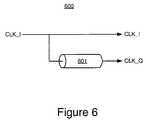
- FIG. 6depicts a propagation delay fixed delay clock generator, according to another embodiment of the present invention.
- FIG. 7is a flowchart of a process for multiplexing data, according to another embodiment of the present invention.
- a multiplexer implemented according to embodiments of the present inventionis capable of high speed operation and exhibits significant insensitivity to supply voltage, temperature and manufacturing process variations.
- Features of the inventionare well-suited for higher-speed multiplexing applications (for example, in high-speed optical networking systems), and overcome timing constraints that can affect such systems.
- Conventional multiplexerscan experience a reduction in timing margin at high frequencies due to the variable delay from clock-to-data (e.g., clock-to-Q) in data latches (e.g., flip-flops or other logic circuit elements).
- This reduction in timing margincan effectively limit the operating frequency to less than half of the inverse of the worst-case clock-to-data delay of a data latch.
- One embodiment of the present inventionaddresses this problem by compensating for the variable delay in the data latches and providing a second clock signal, which is delayed with respect to the first (e.g., in-phase) clock signal, to control selection of data to be multiplexed.
- the second, delayed clock signalcomprises a quadrature-phase clock, the signal of which is displaced in time with respect to the first in-phase clock by a quarter clock cycle (e.g., 90 degrees). This can effectuate a fixed timing relationship to the data signals for operating a selector comprising the multiplexer that improves performance at high frequencies.
- the second clock signalis displaced in time with respect to the first in-phase clock by other than one quarter clock period. In one embodiment, the second clock signal is displaced in time with respect to the first in-phase clock by approximately one quarter clock period.
- logic circuit elementor “binary circuit element” include logic and circuit elements that maintain, or alternate between, one of two states (e.g., a binary zero and a binary one).
- embodiments of the inventionare described using the term “latches.”
- embodiments of the present inventionmay be used with other types of devices that perform the same general function as a multiplexer; that is, the selection of a signal from one or more of a plurality of input (e.g., data) lines.
- FIG. 2illustrates a multiplexer 200 employing delay compensation.
- a delay-compensating buffer 201is in series with the clock signal CLK and the selector 205 in multiplexer 200 . Where the delay of the buffer 201 is chosen to approximately match the clock-to-data delay of the first and second data latches 202 , the resulting delayed clock CLK_D has edges that are approximately aligned with transitions in the input data streams D 1 and D 2 , as illustrated in timing diagram 203 .
- a third latch 209delays D 2 by one-half clock cycle, relative to D 1 .
- delay compensating buffer 201it is advantageous for delay compensating buffer 201 to have a delay approximately matching the clock-to-data delay of the data latches over voltage, temperature, manufacturing process and other variations. Such matching provides a fixed timing relationship between clock and data waveforms in multiplexer 200 .
- the condition wherein the delay of the compensating buffer 201 approximately matches the clock-to-data delay of latches 202is referred to “full delay matching” for convenience. There are several ways that one can achieve such delay matching in practice.
- full delay matching between clock and data waveformscan be achieved by a replica technique, known in the art.
- Replica delay matchingcan be effectuated by constructing delay compensating buffer 201 using circuitry that effectively duplicates the circuitry in the data latches 202 .
- the compensated clock edgestrack the data transition edges as conditions vary so that the relative timing of the edges is held approximately constant (e.g., effectively invariant with respect to each other).
- Other techniques for providing matched delayscan also be used.
- FIG. 3depicts a multiplexer 300 , according to one embodiment of the present invention.
- Multiplexer 300makes use of an additional clock signal CLK_Q to operate selector 305 .
- the clock signal CLK_Qis offset or delayed by a fixed amount of time with respect to the initial clock signal, now referred to as CLK_I.
- CLK_Iis in-phase with the transitions of latches 302 and the data signals D 1 and D 2 .
- CLK_Qis a quadrature clock signal generated by a quadrature clock generator (e.g., quadrature clock generators 400 , 500 , 600 ; FIGS. 4 , 5 , 6 , respectively).
- a third latch 309delays D 2 by one half clock cycle, relative to D 1 .
- CLK_Qis delayed by a fixed amount other than a quadrature delay.
- a quadrature clock signal CLK_Qhas a fixed timing relationship with respect to the in-phase clock signal CLK_I.
- a quadrature clockhas a rising edge that is shifted by a quarter of the clock period (e.g., 90 degrees) with respect to the rising edge of the in-phase clock.
- the quadrature clockis delayed by the delay compensating buffer 301 and applied to the selector 305 control port. As shown in the timing diagram 303 , the delay-compensated quadrature clock is positioned so that its active-low and active-high intervals occur in the middle of the stable intervals of data signals D 1 and D 2 .
- this timing relationship between the selector clock CLK_Q and input data D 1 and D 2maximizes the timing margin and the stability of the timing relationship and enables reliable, high speed operation with minimal sensitivity to the supply voltage, temperature, process and other variations that can occur in practice.
- a quadrature clock signal CLK_Qis further advantageous in that the fixed timing relationship with respect to the in-phase clock signal is a fixed fraction of the clock period, independent of the operating frequency. This property stabilizes the selector clock alignment over a wide range of operating frequencies and effectively substantially eliminates the multiplexer speed limitation arising from finite clock-to-data delay in the data latches.
- the second clock signalis displaced in time with respect to the first in-phase clock by other than one quarter clock period. In one embodiment, the second clock signal is displaced in time with respect to the first in-phase clock by approximately one quarter clock period.
- quadratureis used herein to discuss the time displacement of the delayed clock signal CLK_Q with respect to CLK_I for any embodiment, whether delay of CLK_Q with respect to CLK_I is true quadrature, approximately quadrature, or other than quadrature.
- the clock-to-data delay of the data latches 302may be suitably small such that delay compensation becomes unnecessary.
- the delay compensation buffermay be omitted, thereby simplifying the circuitry while retaining the benefits imparted by the use of the fixed-delay (e.g. quadrature) clock for operating (e.g. clocking) the selector 305 .
- the use of a quadrature selector clock without the delay compensating buffer 301retains the advantage that the timing margin of the selector clock relative to the data transitions is nearly maximized.
- FIG. 3depicts an embodiment using a quadrature clock
- clocksthat generate signals other than quadrature but at some fixed delay relative to the in-phase clock
- clock signal CLK_Qcan be a fixed delay other than one-quarter clock cycle (e.g., other than 90 degrees).
- quadrature clock signals or clock signals other than quadrature with a fixed delay relative to another clock signal in phase with data signalsare described in conjunction with FIGS. 4 , 5 , and 6 .
- the quadrature (or other fixed delay) relationshipis rendered with accuracy, because deviations therefrom can adversely affect the corresponding timing margin. For instance, in an embodiment utilizing a quadrature-based delay, a deviation from a precise quadrature relationship between the delay clock signal and the in-phase clock signal can reduce the resulting timing margin of the multiplexer.
- a pair 400 of coupled oscillators 401 and 402generate an in-phase clock, CLK_I, and a fixed-delay clock signal CLK_Q in one embodiment.
- Such fixed-delay clock generation by coupled oscillatorscan be implemented as taught by U.S. Pat. No. 6,188,292, which is incorporated herein by reference as explanatory material only.
- FIG. 5depicts a clocking system 500 , wherein a single clock 501 operates at twice the frequency of an in-phase clock signal CLK_I and an exemplary quadrature clock signal CLK_Q.
- the output signal 2CLK of clock 501is applied to a “divide-by-two” circuit 502 to derive the in-phase and quadrature (or other fixed delay) clock signals at separate points.
- FIG. 5depicts a divide-by-two circuit employing two interconnected data latches 502 , other embodiments use alternative arrangements of circuit devices, as is known in the art.
- FIG. 6depicts a clocking system 600 wherein in-phase clock signal CLK_I is provided on one line and is also delayed by routing through a section of transmission line 601 to render a second, delayed clock signal CLK_Q.
- the delay relationship between signals CLK_I and CLK_Qis fixed at some desired value.
- the propagation delay of the transmission line section 601 itselfthus provides the required fixed timing offset.
- the delay relationship between signals CLK_I and CLK_Qis fixed at, for instance, a quadrature-based value.
- the length of section 601can be quite large. However, this technique remains practical at high frequency data rates. At lower frequency data rates, other passive circuit networks comprising resistors, inductors, capacitors and other passive electrical elements can be used to provide a fixed delay in place of the transmission line section 601 , as is known in the art. Other techniques for generating a clock signal having a fixed delay relative to an in-phase clock such as a quadrature clock can be used, as well.
- Process 700begins with step 701 , wherein in-phase and fixed-delay clock signals are provided. These clock signals may be provided using techniques described in FIGS. 4-6 , for example, or using other techniques known in the art.
- the fixed-delay clock signalis a quadrature clock signal.
- step 702data signals with transitions synchronized to the in-phase clock are generated. These data signals may be generated using flip-flops, latches (e.g. latches 302 ; FIG. 3 ), or similar registers or logic elements, or using other techniques that are known in the art. In practice, the process step 702 of generating these data signals may result in some unwanted time delay between the in-phase clock and the data signal transitions.
- any unwanted time delayis compensated for by delaying the fixed-delay clock signal by an amount approximately matching any unwanted time delay between in-phase clock and data signal transitions.
- This compensating delaymay be generated using a variety of techniques known in the art.
- the compensating delayis generated by passing the fixed-delay clock through a delay-compensating buffer (e.g. buffer 301 ; FIG. 3 ).
- the compensating delaycorresponds to a clock-to-data delay of a data latch used to generate the data signals in step 702 .
- the unwanted time delaymay be small enough that step 703 may be omitted.
- the compensated (if applicable), fixed-delay clockis used to select between data signals for output.
- this selectioncan be effectuated by operating (e.g. clocking) a data signal selector (e.g. selector 305 ; FIG. 3 ) based on the delay-compensated fixed-delay (e.g. quadrature) clock signal.
- the selectionmay employ the fixed-delay clock signal directly without further compensation.
- embodiments of the present inventionprovide circuits and methods for multiplexing data that are capable of high speed operation with acceptable timing margins and reduced sensitivity to electrical and other variations that functions by compensating for clock-to-data delay in latch transitions in clocking a selector that sequentially selects data signals from those latches for output.
- the delay compensationcan closely match the clock-to-data delay of the latches.
- One embodimentprovides a circuit and method for multiplexing capable of high speed operation with acceptable timing margins and reduced sensitivity to electrical and other variations that functions by clocking latch transitions with a first clock signal and clocking a selector that sequentially selects data signals from those latches for output with a second clock signal.
- the second clock signalhas a fixed delay, relative to the first clock signal.
- the second clock signalcomprises a clock that is offset in time from the first clock by a quarter clock cycle (e.g., a quadrature clock).
- a quarter clock cyclee.g., a quadrature clock
Landscapes
- Engineering & Computer Science (AREA)
- Computer Networks & Wireless Communication (AREA)
- Signal Processing (AREA)
- Theoretical Computer Science (AREA)
- Microelectronics & Electronic Packaging (AREA)
- Pulse Circuits (AREA)
Abstract
Description
Claims (25)
Priority Applications (1)
| Application Number | Priority Date | Filing Date | Title |
|---|---|---|---|
| US10/623,028US7764715B2 (en) | 2002-08-30 | 2003-07-17 | Circuits and methods for data multiplexing |
Applications Claiming Priority (2)
| Application Number | Priority Date | Filing Date | Title |
|---|---|---|---|
| US40755802P | 2002-08-30 | 2002-08-30 | |
| US10/623,028US7764715B2 (en) | 2002-08-30 | 2003-07-17 | Circuits and methods for data multiplexing |
Publications (2)
| Publication Number | Publication Date |
|---|---|
| US20040042503A1 US20040042503A1 (en) | 2004-03-04 |
| US7764715B2true US7764715B2 (en) | 2010-07-27 |
Family
ID=31981527
Family Applications (1)
| Application Number | Title | Priority Date | Filing Date |
|---|---|---|---|
| US10/623,028Active2027-05-13US7764715B2 (en) | 2002-08-30 | 2003-07-17 | Circuits and methods for data multiplexing |
Country Status (1)
| Country | Link |
|---|---|
| US (1) | US7764715B2 (en) |
Cited By (1)
| Publication number | Priority date | Publication date | Assignee | Title |
|---|---|---|---|---|
| US10944407B1 (en)* | 2020-06-03 | 2021-03-09 | Stmicroelectronics International N.V. | Source synchronous interface with selectable delay on source and delay on destination control |
Families Citing this family (28)
| Publication number | Priority date | Publication date | Assignee | Title |
|---|---|---|---|---|
| US8796830B1 (en) | 2006-09-01 | 2014-08-05 | Google Inc. | Stackable low-profile lead frame package |
| US8397013B1 (en) | 2006-10-05 | 2013-03-12 | Google Inc. | Hybrid memory module |
| US8041881B2 (en) | 2006-07-31 | 2011-10-18 | Google Inc. | Memory device with emulated characteristics |
| US8060774B2 (en) | 2005-06-24 | 2011-11-15 | Google Inc. | Memory systems and memory modules |
| US8081474B1 (en) | 2007-12-18 | 2011-12-20 | Google Inc. | Embossed heat spreader |
| US7609567B2 (en)* | 2005-06-24 | 2009-10-27 | Metaram, Inc. | System and method for simulating an aspect of a memory circuit |
| US8055833B2 (en) | 2006-10-05 | 2011-11-08 | Google Inc. | System and method for increasing capacity, performance, and flexibility of flash storage |
| US8386722B1 (en)* | 2008-06-23 | 2013-02-26 | Google Inc. | Stacked DIMM memory interface |
| US9171585B2 (en) | 2005-06-24 | 2015-10-27 | Google Inc. | Configurable memory circuit system and method |
| US8111566B1 (en) | 2007-11-16 | 2012-02-07 | Google, Inc. | Optimal channel design for memory devices for providing a high-speed memory interface |
| US8077535B2 (en) | 2006-07-31 | 2011-12-13 | Google Inc. | Memory refresh apparatus and method |
| US8438328B2 (en)* | 2008-02-21 | 2013-05-07 | Google Inc. | Emulation of abstracted DIMMs using abstracted DRAMs |
| US8130560B1 (en) | 2006-11-13 | 2012-03-06 | Google Inc. | Multi-rank partial width memory modules |
| US20080028136A1 (en)* | 2006-07-31 | 2008-01-31 | Schakel Keith R | Method and apparatus for refresh management of memory modules |
| US20080082763A1 (en) | 2006-10-02 | 2008-04-03 | Metaram, Inc. | Apparatus and method for power management of memory circuits by a system or component thereof |
| US8244971B2 (en) | 2006-07-31 | 2012-08-14 | Google Inc. | Memory circuit system and method |
| US8089795B2 (en) | 2006-02-09 | 2012-01-03 | Google Inc. | Memory module with memory stack and interface with enhanced capabilities |
| US8335894B1 (en) | 2008-07-25 | 2012-12-18 | Google Inc. | Configurable memory system with interface circuit |
| US9542352B2 (en) | 2006-02-09 | 2017-01-10 | Google Inc. | System and method for reducing command scheduling constraints of memory circuits |
| US7386656B2 (en) | 2006-07-31 | 2008-06-10 | Metaram, Inc. | Interface circuit system and method for performing power management operations in conjunction with only a portion of a memory circuit |
| US8327104B2 (en) | 2006-07-31 | 2012-12-04 | Google Inc. | Adjusting the timing of signals associated with a memory system |
| US10013371B2 (en) | 2005-06-24 | 2018-07-03 | Google Llc | Configurable memory circuit system and method |
| US8359187B2 (en) | 2005-06-24 | 2013-01-22 | Google Inc. | Simulating a different number of memory circuit devices |
| US9507739B2 (en) | 2005-06-24 | 2016-11-29 | Google Inc. | Configurable memory circuit system and method |
| WO2007028109A2 (en) | 2005-09-02 | 2007-03-08 | Metaram, Inc. | Methods and apparatus of stacking drams |
| US9632929B2 (en)* | 2006-02-09 | 2017-04-25 | Google Inc. | Translating an address associated with a command communicated between a system and memory circuits |
| US8044833B2 (en)* | 2009-01-16 | 2011-10-25 | Raytheon Company | High speed serializer |
| DE202010017690U1 (en) | 2009-06-09 | 2012-05-29 | Google, Inc. | Programming dimming terminating resistor values |
Citations (8)
| Publication number | Priority date | Publication date | Assignee | Title |
|---|---|---|---|---|
| US5052028A (en)* | 1989-03-31 | 1991-09-24 | Siemens Aktiengesellschaft | Method for synchronizing the phase of clock signals of two clock generators in communications networks |
| US5488641A (en)* | 1992-12-10 | 1996-01-30 | Northern Telecom Limited | Digital phase-locked loop circuit |
| US5534805A (en)* | 1990-12-26 | 1996-07-09 | Mitsubishi Denki Kabushiki Kaisha | Synchronized clock generating apparatus |
| US5850422A (en)* | 1995-07-21 | 1998-12-15 | Symbios, Inc. | Apparatus and method for recovering a clock signal which is embedded in an incoming data stream |
| US6278755B1 (en)* | 1999-05-18 | 2001-08-21 | Nec Corporation | Bit synchronization circuit |
| US6917660B2 (en)* | 2001-06-04 | 2005-07-12 | Intel Corporation | Adaptive de-skew clock generation |
| US6973151B2 (en)* | 2001-02-15 | 2005-12-06 | Intel Corporation | Dynamic phase aligning interface |
| US7221126B1 (en)* | 2000-04-28 | 2007-05-22 | Hewlett-Packard Development Company, L.P. | Apparatus and method to align clocks for repeatable system testing |
- 2003
- 2003-07-17USUS10/623,028patent/US7764715B2/enactiveActive
Patent Citations (8)
| Publication number | Priority date | Publication date | Assignee | Title |
|---|---|---|---|---|
| US5052028A (en)* | 1989-03-31 | 1991-09-24 | Siemens Aktiengesellschaft | Method for synchronizing the phase of clock signals of two clock generators in communications networks |
| US5534805A (en)* | 1990-12-26 | 1996-07-09 | Mitsubishi Denki Kabushiki Kaisha | Synchronized clock generating apparatus |
| US5488641A (en)* | 1992-12-10 | 1996-01-30 | Northern Telecom Limited | Digital phase-locked loop circuit |
| US5850422A (en)* | 1995-07-21 | 1998-12-15 | Symbios, Inc. | Apparatus and method for recovering a clock signal which is embedded in an incoming data stream |
| US6278755B1 (en)* | 1999-05-18 | 2001-08-21 | Nec Corporation | Bit synchronization circuit |
| US7221126B1 (en)* | 2000-04-28 | 2007-05-22 | Hewlett-Packard Development Company, L.P. | Apparatus and method to align clocks for repeatable system testing |
| US6973151B2 (en)* | 2001-02-15 | 2005-12-06 | Intel Corporation | Dynamic phase aligning interface |
| US6917660B2 (en)* | 2001-06-04 | 2005-07-12 | Intel Corporation | Adaptive de-skew clock generation |
Cited By (1)
| Publication number | Priority date | Publication date | Assignee | Title |
|---|---|---|---|---|
| US10944407B1 (en)* | 2020-06-03 | 2021-03-09 | Stmicroelectronics International N.V. | Source synchronous interface with selectable delay on source and delay on destination control |
Also Published As
| Publication number | Publication date |
|---|---|
| US20040042503A1 (en) | 2004-03-04 |
Similar Documents
| Publication | Publication Date | Title |
|---|---|---|
| US7764715B2 (en) | Circuits and methods for data multiplexing | |
| US6359479B1 (en) | Synchronizing data transfers between two distinct clock domains | |
| US10886927B2 (en) | Signal generation circuit synchronized with a clock signal and a semiconductor apparatus using the same | |
| KR100459709B1 (en) | Serializer-deserializer circuit having enough set up and hold time margin | |
| JP3945874B2 (en) | Method for synchronizing signals and structure therefor | |
| JP5707477B2 (en) | Crystal-based oscillators for synchronization systems | |
| US7675797B2 (en) | CAS latency circuit and semiconductor memory device including the same | |
| KR20000006028A (en) | Clock latency compensation circuit for ddr timing | |
| EP1735680A2 (en) | Delay line synchronizer apparatus and method | |
| CN112397116A (en) | Signal generating circuit synchronized with clock signal and semiconductor device using the same | |
| US6255870B1 (en) | Apparatus for compensating locking error in high speed memory device with delay locked loop | |
| KR100399070B1 (en) | Doulble locking delay locked loop clock generation device using ring oscillator | |
| US6993671B2 (en) | High speed clock divider with synchronous phase start-up over physically distributed space | |
| KR100419795B1 (en) | Phase difference magnifier | |
| US12294379B2 (en) | Clock generating circuit and semiconductor apparatus using the same | |
| KR100433648B1 (en) | Delay-matched clock and data signal generator | |
| JP5865533B2 (en) | System employing a synchronized crystal oscillator based clock | |
| US6665218B2 (en) | Self calibrating register for source synchronous clocking systems | |
| KR100792379B1 (en) | Frequency division method of delay locked loop and delay locked loop capable of operating at various frequencies. | |
| US6918047B1 (en) | Apparatus for high data rate synchronous interface using a delay locked loop to synchronize a clock signal and a method thereof | |
| JPH05130094A (en) | Clock transfer circuit | |
| JP2000207051A (en) | Dll clock generator | |
| KR101347283B1 (en) | CAS Latency Circuit and Semiconductor Memory Device having the same | |
| US6552590B2 (en) | Clocking scheme for ASIC | |
| KR20000022911A (en) | A flip-flop circuit and a automatic layout device |
Legal Events
| Date | Code | Title | Description |
|---|---|---|---|
| AS | Assignment | Owner name:BIGBEAR NETWORKS, INC., CALIFORNIA Free format text:ASSIGNMENT OF ASSIGNORS INTEREST;ASSIGNORS:SHAEFFER, DEREK;LEE, MICHELLE;TAO, HAI;REEL/FRAME:014361/0312;SIGNING DATES FROM 20030708 TO 20030714 Owner name:BIGBEAR NETWORKS, INC., CALIFORNIA Free format text:ASSIGNMENT OF ASSIGNORS INTEREST;ASSIGNORS:SHAEFFER, DEREK;LEE, MICHELLE;TAO, HAI;SIGNING DATES FROM 20030708 TO 20030714;REEL/FRAME:014361/0312 | |
| AS | Assignment | Owner name:FINISAR CORPORATION, CALIFORNIA Free format text:ASSIGNMENT OF ASSIGNORS INTEREST;ASSIGNOR:BIG BEAR NETWORKS, INC.;REEL/FRAME:017057/0222 Effective date:20051115 | |
| STCF | Information on status: patent grant | Free format text:PATENTED CASE | |
| FPAY | Fee payment | Year of fee payment:4 | |
| MAFP | Maintenance fee payment | Free format text:PAYMENT OF MAINTENANCE FEE, 8TH YEAR, LARGE ENTITY (ORIGINAL EVENT CODE: M1552) Year of fee payment:8 | |
| AS | Assignment | Owner name:BANK OF AMERICA, N.A., AS ADMINISTRATIVE AGENT, NO Free format text:NOTICE OF GRANT OF SECURITY INTEREST IN PATENTS;ASSIGNORS:II-VI INCORPORATED;MARLOW INDUSTRIES, INC.;EPIWORKS, INC.;AND OTHERS;REEL/FRAME:050484/0204 Effective date:20190924 Owner name:BANK OF AMERICA, N.A., AS ADMINISTRATIVE AGENT, NORTH CAROLINA Free format text:NOTICE OF GRANT OF SECURITY INTEREST IN PATENTS;ASSIGNORS:II-VI INCORPORATED;MARLOW INDUSTRIES, INC.;EPIWORKS, INC.;AND OTHERS;REEL/FRAME:050484/0204 Effective date:20190924 | |
| AS | Assignment | Owner name:II-VI DELAWARE, INC., DELAWARE Free format text:ASSIGNMENT OF ASSIGNORS INTEREST;ASSIGNOR:FINISAR CORPORATION;REEL/FRAME:052286/0001 Effective date:20190924 | |
| MAFP | Maintenance fee payment | Free format text:PAYMENT OF MAINTENANCE FEE, 12TH YEAR, LARGE ENTITY (ORIGINAL EVENT CODE: M1553); ENTITY STATUS OF PATENT OWNER: LARGE ENTITY Year of fee payment:12 | |
| AS | Assignment | Owner name:JPMORGAN CHASE BANK, N.A., AS COLLATERAL AGENT, NEW YORK Free format text:SECURITY INTEREST;ASSIGNORS:II-VI INCORPORATED;II-VI DELAWARE, INC.;M CUBED TECHNOLOGIES, INC.;AND OTHERS;REEL/FRAME:060562/0254 Effective date:20220701 | |
| AS | Assignment | Owner name:PHOTOP TECHNOLOGIES, INC., CALIFORNIA Free format text:PATENT RELEASE AND REASSIGNMENT;ASSIGNOR:BANK OF AMERICA, N.A., AS ADMINISTRATIVE AGENT;REEL/FRAME:060574/0001 Effective date:20220701 Owner name:II-VI OPTOELECTRONIC DEVICES, INC., NEW JERSEY Free format text:PATENT RELEASE AND REASSIGNMENT;ASSIGNOR:BANK OF AMERICA, N.A., AS ADMINISTRATIVE AGENT;REEL/FRAME:060574/0001 Effective date:20220701 Owner name:II-VI DELAWARE, INC., PENNSYLVANIA Free format text:PATENT RELEASE AND REASSIGNMENT;ASSIGNOR:BANK OF AMERICA, N.A., AS ADMINISTRATIVE AGENT;REEL/FRAME:060574/0001 Effective date:20220701 Owner name:II-VI PHOTONICS (US), INC., MASSACHUSETTS Free format text:PATENT RELEASE AND REASSIGNMENT;ASSIGNOR:BANK OF AMERICA, N.A., AS ADMINISTRATIVE AGENT;REEL/FRAME:060574/0001 Effective date:20220701 Owner name:M CUBED TECHNOLOGIES, INC., CONNECTICUT Free format text:PATENT RELEASE AND REASSIGNMENT;ASSIGNOR:BANK OF AMERICA, N.A., AS ADMINISTRATIVE AGENT;REEL/FRAME:060574/0001 Effective date:20220701 Owner name:II-VI OPTICAL SYSTEMS, INC., CALIFORNIA Free format text:PATENT RELEASE AND REASSIGNMENT;ASSIGNOR:BANK OF AMERICA, N.A., AS ADMINISTRATIVE AGENT;REEL/FRAME:060574/0001 Effective date:20220701 Owner name:FINISAR CORPORATION, CALIFORNIA Free format text:PATENT RELEASE AND REASSIGNMENT;ASSIGNOR:BANK OF AMERICA, N.A., AS ADMINISTRATIVE AGENT;REEL/FRAME:060574/0001 Effective date:20220701 Owner name:OPTIUM CORPORATION, CALIFORNIA Free format text:PATENT RELEASE AND REASSIGNMENT;ASSIGNOR:BANK OF AMERICA, N.A., AS ADMINISTRATIVE AGENT;REEL/FRAME:060574/0001 Effective date:20220701 Owner name:COADNA PHOTONICS, INC., PENNSYLVANIA Free format text:PATENT RELEASE AND REASSIGNMENT;ASSIGNOR:BANK OF AMERICA, N.A., AS ADMINISTRATIVE AGENT;REEL/FRAME:060574/0001 Effective date:20220701 Owner name:KAILIGHT PHOTONICS, INC., CALIFORNIA Free format text:PATENT RELEASE AND REASSIGNMENT;ASSIGNOR:BANK OF AMERICA, N.A., AS ADMINISTRATIVE AGENT;REEL/FRAME:060574/0001 Effective date:20220701 Owner name:LIGHTSMYTH TECHNOLOGIES, INC., OREGON Free format text:PATENT RELEASE AND REASSIGNMENT;ASSIGNOR:BANK OF AMERICA, N.A., AS ADMINISTRATIVE AGENT;REEL/FRAME:060574/0001 Effective date:20220701 Owner name:EPIWORKS, INC., ILLINOIS Free format text:PATENT RELEASE AND REASSIGNMENT;ASSIGNOR:BANK OF AMERICA, N.A., AS ADMINISTRATIVE AGENT;REEL/FRAME:060574/0001 Effective date:20220701 Owner name:MARLOW INDUSTRIES, INC., TEXAS Free format text:PATENT RELEASE AND REASSIGNMENT;ASSIGNOR:BANK OF AMERICA, N.A., AS ADMINISTRATIVE AGENT;REEL/FRAME:060574/0001 Effective date:20220701 Owner name:II-VI INCORPORATED, PENNSYLVANIA Free format text:PATENT RELEASE AND REASSIGNMENT;ASSIGNOR:BANK OF AMERICA, N.A., AS ADMINISTRATIVE AGENT;REEL/FRAME:060574/0001 Effective date:20220701 |