US7760519B2 - Primary only control quasi resonant convertor - Google Patents
Primary only control quasi resonant convertorDownload PDFInfo
- Publication number
- US7760519B2 US7760519B2US12/079,815US7981508AUS7760519B2US 7760519 B2US7760519 B2US 7760519B2US 7981508 AUS7981508 AUS 7981508AUS 7760519 B2US7760519 B2US 7760519B2
- Authority
- US
- United States
- Prior art keywords
- primary
- coupled
- circuit
- switching element
- converter
- Prior art date
- Legal status (The legal status is an assumption and is not a legal conclusion. Google has not performed a legal analysis and makes no representation as to the accuracy of the status listed.)
- Active, expires
Links
Images


Classifications
- H—ELECTRICITY
- H02—GENERATION; CONVERSION OR DISTRIBUTION OF ELECTRIC POWER
- H02M—APPARATUS FOR CONVERSION BETWEEN AC AND AC, BETWEEN AC AND DC, OR BETWEEN DC AND DC, AND FOR USE WITH MAINS OR SIMILAR POWER SUPPLY SYSTEMS; CONVERSION OF DC OR AC INPUT POWER INTO SURGE OUTPUT POWER; CONTROL OR REGULATION THEREOF
- H02M3/00—Conversion of DC power input into DC power output
- H02M3/22—Conversion of DC power input into DC power output with intermediate conversion into AC
- H02M3/24—Conversion of DC power input into DC power output with intermediate conversion into AC by static converters
- H02M3/28—Conversion of DC power input into DC power output with intermediate conversion into AC by static converters using discharge tubes with control electrode or semiconductor devices with control electrode to produce the intermediate AC
- H02M3/325—Conversion of DC power input into DC power output with intermediate conversion into AC by static converters using discharge tubes with control electrode or semiconductor devices with control electrode to produce the intermediate AC using devices of a triode or a transistor type requiring continuous application of a control signal
- H02M3/335—Conversion of DC power input into DC power output with intermediate conversion into AC by static converters using discharge tubes with control electrode or semiconductor devices with control electrode to produce the intermediate AC using devices of a triode or a transistor type requiring continuous application of a control signal using semiconductor devices only
- H02M3/33507—Conversion of DC power input into DC power output with intermediate conversion into AC by static converters using discharge tubes with control electrode or semiconductor devices with control electrode to produce the intermediate AC using devices of a triode or a transistor type requiring continuous application of a control signal using semiconductor devices only with automatic control of the output voltage or current, e.g. flyback converters
- H02M3/33523—Conversion of DC power input into DC power output with intermediate conversion into AC by static converters using discharge tubes with control electrode or semiconductor devices with control electrode to produce the intermediate AC using devices of a triode or a transistor type requiring continuous application of a control signal using semiconductor devices only with automatic control of the output voltage or current, e.g. flyback converters with galvanic isolation between input and output of both the power stage and the feedback loop
- H—ELECTRICITY
- H02—GENERATION; CONVERSION OR DISTRIBUTION OF ELECTRIC POWER
- H02M—APPARATUS FOR CONVERSION BETWEEN AC AND AC, BETWEEN AC AND DC, OR BETWEEN DC AND DC, AND FOR USE WITH MAINS OR SIMILAR POWER SUPPLY SYSTEMS; CONVERSION OF DC OR AC INPUT POWER INTO SURGE OUTPUT POWER; CONTROL OR REGULATION THEREOF
- H02M3/00—Conversion of DC power input into DC power output
- H02M3/01—Resonant DC/DC converters
- H—ELECTRICITY
- H02—GENERATION; CONVERSION OR DISTRIBUTION OF ELECTRIC POWER
- H02M—APPARATUS FOR CONVERSION BETWEEN AC AND AC, BETWEEN AC AND DC, OR BETWEEN DC AND DC, AND FOR USE WITH MAINS OR SIMILAR POWER SUPPLY SYSTEMS; CONVERSION OF DC OR AC INPUT POWER INTO SURGE OUTPUT POWER; CONTROL OR REGULATION THEREOF
- H02M3/00—Conversion of DC power input into DC power output
- H02M3/22—Conversion of DC power input into DC power output with intermediate conversion into AC
- H02M3/24—Conversion of DC power input into DC power output with intermediate conversion into AC by static converters
- H02M3/28—Conversion of DC power input into DC power output with intermediate conversion into AC by static converters using discharge tubes with control electrode or semiconductor devices with control electrode to produce the intermediate AC
- H02M3/325—Conversion of DC power input into DC power output with intermediate conversion into AC by static converters using discharge tubes with control electrode or semiconductor devices with control electrode to produce the intermediate AC using devices of a triode or a transistor type requiring continuous application of a control signal
- H02M3/335—Conversion of DC power input into DC power output with intermediate conversion into AC by static converters using discharge tubes with control electrode or semiconductor devices with control electrode to produce the intermediate AC using devices of a triode or a transistor type requiring continuous application of a control signal using semiconductor devices only
- H02M3/33569—Conversion of DC power input into DC power output with intermediate conversion into AC by static converters using discharge tubes with control electrode or semiconductor devices with control electrode to produce the intermediate AC using devices of a triode or a transistor type requiring continuous application of a control signal using semiconductor devices only having several active switching elements
- H02M3/33571—Half-bridge at primary side of an isolation transformer
- H—ELECTRICITY
- H02—GENERATION; CONVERSION OR DISTRIBUTION OF ELECTRIC POWER
- H02M—APPARATUS FOR CONVERSION BETWEEN AC AND AC, BETWEEN AC AND DC, OR BETWEEN DC AND DC, AND FOR USE WITH MAINS OR SIMILAR POWER SUPPLY SYSTEMS; CONVERSION OF DC OR AC INPUT POWER INTO SURGE OUTPUT POWER; CONTROL OR REGULATION THEREOF
- H02M3/00—Conversion of DC power input into DC power output
- H02M3/22—Conversion of DC power input into DC power output with intermediate conversion into AC
- H02M3/24—Conversion of DC power input into DC power output with intermediate conversion into AC by static converters
- H02M3/28—Conversion of DC power input into DC power output with intermediate conversion into AC by static converters using discharge tubes with control electrode or semiconductor devices with control electrode to produce the intermediate AC
- H02M3/325—Conversion of DC power input into DC power output with intermediate conversion into AC by static converters using discharge tubes with control electrode or semiconductor devices with control electrode to produce the intermediate AC using devices of a triode or a transistor type requiring continuous application of a control signal
- H02M3/335—Conversion of DC power input into DC power output with intermediate conversion into AC by static converters using discharge tubes with control electrode or semiconductor devices with control electrode to produce the intermediate AC using devices of a triode or a transistor type requiring continuous application of a control signal using semiconductor devices only
- H02M3/33569—Conversion of DC power input into DC power output with intermediate conversion into AC by static converters using discharge tubes with control electrode or semiconductor devices with control electrode to produce the intermediate AC using devices of a triode or a transistor type requiring continuous application of a control signal using semiconductor devices only having several active switching elements
- H02M3/33573—Full-bridge at primary side of an isolation transformer
- Y—GENERAL TAGGING OF NEW TECHNOLOGICAL DEVELOPMENTS; GENERAL TAGGING OF CROSS-SECTIONAL TECHNOLOGIES SPANNING OVER SEVERAL SECTIONS OF THE IPC; TECHNICAL SUBJECTS COVERED BY FORMER USPC CROSS-REFERENCE ART COLLECTIONS [XRACs] AND DIGESTS
- Y02—TECHNOLOGIES OR APPLICATIONS FOR MITIGATION OR ADAPTATION AGAINST CLIMATE CHANGE
- Y02B—CLIMATE CHANGE MITIGATION TECHNOLOGIES RELATED TO BUILDINGS, e.g. HOUSING, HOUSE APPLIANCES OR RELATED END-USER APPLICATIONS
- Y02B70/00—Technologies for an efficient end-user side electric power management and consumption
- Y02B70/10—Technologies improving the efficiency by using switched-mode power supplies [SMPS], i.e. efficient power electronics conversion e.g. power factor correction or reduction of losses in power supplies or efficient standby modes
Definitions
- the present inventionrelates to the field of power supplies. More particularly, the present invention relates to a primary only controlled quasi resonant converter.
- a voltage regulatorIn many applications a voltage regulator is required to provide a voltage within a predetermined range. Some circuits are subject to uncertain and undesirable functioning and even irreparable damage if an input power supply fall outside a certain range.
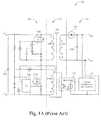
- FIG. 1A functional block diagram of a prior art power supply apparatus 10 is shown in FIG. 1 .
- the apparatus 10generally includes a power converter 12 coupled with a transformer 14 that is coupled with an output rectifier 16 .
- the output rectifier 16is coupled with an output capacitor 19 at an output Vout.
- a regulation circuit 15comprising an opto-coupler 17 and a voltage reference and error amplifier 18 is coupled between the voltage converter 12 and the output Vout.
- the power converter 12is configured to receive an unregulated DC voltage signal.
- the unregulated DC voltage signalis coupled to the transformer 14 .
- the transformer 14includes a primary 14 P and a secondary 14 S.
- the unregulated DC voltage signaldrives the primary 14 P to produce an intermediate voltage signal.
- the intermediate voltage signalcomprises a stepped-up or stepped-down voltage signal derived from the voltage signal that drove the primary 14 P.
- the intermediate voltage signalis coupled to the output rectifier 16 .
- the output rectifier 16rectifies the intermediate voltage signal to produce a regulated DC output voltage signal.
- a feedback signal provided by the opto-coupler 17is coupled to the power converter for regulating the output voltage Vout.
- FIG. 1AA schematic diagram of a prior art regulated power supply 100 is shown in FIG. 1A .
- the power supply 100includes a converter circuit 102 coupled with a transformer 140 .
- the transformer 140is coupled with an output circuit 106 .
- the converter circuit 102includes a capacitor 110 coupled across an input Vin and coupled with a primary 140 P 1 and 140 P 2 of the transformer 140 .
- a primary switch 112 A and an auxiliary switch 112 Bare coupled with the primary 140 P 1 and 140 P 2 respectively.
- a pulse width modulator (PWM) module 130is coupled with a gate of the primary switch 112 A.
- the output circuit 106includes an output rectifying diode 146 and a load or an output capacitor 150 coupled across a secondary 140 S of the transformer 140 .
- the power supply 100can include a voltage regulating circuit including optical coupler circuit 108 and a voltage reference and error amplifier 109 .
- the power supply 100uses the PWM module 130 to alter a duty cycle of the primary switch 112 A.
- the optical coupler circuit 108in cooperation with the voltage reference and error amplifier 109 provides feedback to the PWM module 130 .
- the PWM module 130accordingly adjusts the duty cycle of the primary switch 112 A to compensate for any variances in an output voltage Vout.
- Very often the point of failure for the power supply 100is the opto-coupler 108 .
- the opto-coupler 108 and the voltage reference and error amplifier 109increase production cost of the power supply 100 .
- a power supply apparatusin accordance with a first aspect of the present invention, includes a converter circuit including a primary switching element and an auxiliary switching element.
- the auxiliary switching elementis for transferring a reflected voltage signal.
- a transformerincludes a primary and a secondary, the primary is coupled with the converter circuit.
- the primaryincludes a single winding and the secondary includes a single winding.
- An output rectifier circuitis coupled with the secondary of the transformer.
- a resonant circuitis included in the converter circuit, the resonant circuit is coupled with the primary.
- the resonant circuitincludes one or more resonance capacitors where the one or more resonance capacitors are configured for providing a transformer resonance.
- the transformer resonancecomprises the reflected voltage signal, the capacitance of the one or more resonance capacitors and a parasitic capacitance of the transformer.
- the reflected voltage signalis received at the resonant circuit via the auxiliary switching element.
- the reflected voltage signalis reflected from the secondary to the primary.
- the power supply apparatusincludes a virtual output voltage feedback loop providing an output voltage reference signal to the converter circuit via a voltage feedback circuit.
- the output voltage reference signalis generated from the reflected voltage signal.
- the converter circuitis responsive to the output voltage reference signal in regulating an output voltage.
- the voltage feedback circuitincludes a voltage divider coupled with the controller and coupled with the primary for sampling the reflected voltage.
- the primary switching element and the auxiliary switching elementeach comprise an n-type MOSFET transistor.
- the first and the second resonance capacitorsare coupled in parallel with the primary.
- a controllerincludes a pulse width modulation (PWM) circuit coupled with the primary switching element.
- the converter circuitcomprises a flyback converter.
- the converter circuitcan comprise one of a forward converter, a push-pull converter, a half bridge converter and a full bridge converter.
- a method of regulating a power supply apparatusincludes generating a reflected voltage signal in a transformer comprising a primary and a secondary.
- the reflected voltage signalis reflected from the secondary to the primary where the primary is coupled with a converter circuit.
- the primaryincludes a single winding and the secondary includes a single winding.
- the reflected voltage signalis transferred from the primary to the converter circuit.
- the converter circuitincludes a primary switching element and an auxiliary switching element.
- the auxiliary switching elementis for transferring the reflected voltage signal.
- a transformer resonanceis generated with a resonant circuit included in the converter circuit.
- the resonant circuitis coupled with the primary.
- the resonant circuitincludes one or more resonance capacitors where the one or more resonance capacitors are configured for providing the transformer resonance.
- the transformer resonancecomprises the reflected voltage signal, the capacitance of the one or more resonance capacitors and a parasitic capacitance of the transformer.
- FIG. 1illustrates a prior art functional block diagram of a power supply apparatus.
- FIG. 1Aillustrates a prior art schematic diagram of a power supply apparatus.
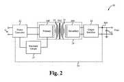
- FIG. 2illustrates a functional block diagram of a power supply apparatus in accordance with an embodiment of the invention.
- FIG. 3illustrates a schematic diagram of a power supply apparatus in accordance with an embodiment of the invention.
- FIG. 4illustrates a schematic diagram of a power supply apparatus in accordance with an alternative embodiment of the invention.
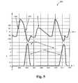
- FIG. 5illustrates a waveform diagram of a power supply apparatus in accordance with an embodiment of the invention.
- FIG. 6illustrates a process flow diagram of a method of regulating a power supply apparatus in accordance with an embodiment of the invention.
- the apparatus 20generally includes a power converter 22 coupled with a transformer 24 that is coupled with an output rectifier 26 .
- the output rectifier 26is coupled with an output capacitor 32 .
- the power converter 22 and the transformer 24include a resonant circuit 27 coupled there between.
- a virtual feedback loop 23is coupled between the power converter 22 and the output capacitor 32 .
- the power converter 22is configured to receive an unregulated DC voltage signal.
- the unregulated DC voltage signalis coupled to the transformer 24 .
- the transformer 24includes a primary 24 P and a secondary 24 S.
- the unregulated DC voltage signaldrives the primary 24 P to produce an intermediate voltage signal.
- the intermediate voltage signalcomprises a stepped-up or stepped-down voltage signal derived from the voltage signal that drove the primary 24 P.
- the intermediate voltage signalis coupled to the output rectifier 26 .
- the output rectifier 26rectifies the intermediate voltage signal to produce a DC output voltage signal.
- a transformer resonanceis generated in the transformer 24 using a reflected voltage signal and a parasitic capacitance, both qualities of the transformer 24 , as an energy source.
- the reflected voltage signal 25is reflected from the secondary 24 S to the primary 24 P.
- the reflected voltage signalis transferred from the primary 24 P to the power converter 22 via the resonant circuit 27 .
- the resonant circuit 27facilitates the transformer resonance by providing capacitive circuits used to exchange energy between the primary 24 P and the resonant circuit 27 .
- the reflected voltage signal 25is used as an output voltage reference signal of the output voltage Vout to regulate the power converter 22 .
- the virtual feedback loop 23is realized by the resonant circuit 27 in cooperation with the primary 24 P and the power converter 22 .
- the apparatus 300generally includes a converter circuit 302 coupled with a transformer 340 that is coupled with an output circuit 306 .
- the output circuit 306is coupled with an output node Vout.
- a virtual output voltage feedback loop 323is coupled between the converter circuit 302 and the output node Vout.
- the power supply apparatus 300is configured to receive an unregulated DC voltage signal at an input node Vin and to provide a regulated output voltage Vout that is suitable for many low voltage appliances such as computer laptops, cell phones and other hand held devices.
- the output voltage Voutcan be set within the range 5-40 VDC.
- the power supply apparatus 300can provide the output voltage Vout that is less than 5 VDC.
- the converter circuit 302is configured to receive the unregulated DC voltage signal.
- the converter circuit 302includes a power converter 322 and a resonant circuit 327 .
- the converter circuit 302comprises a flyback converter.
- the converter circuit 302can comprise one of a forward converter, a push-pull converter, a half-bridge converter and a full-bridge converter.
- the converter circuit 302can comprise other configurations of switch mode power supplies known to a person of skill in the art.
- the resonant circuit 327is coupled between a primary 340 P of the transformer 340 and the power converter 322 .
- the power converter 322includes a first terminal of a primary switching element or primary switch 312 coupled to the input node Vin.
- a second terminal of the primary switch 312is coupled with a controller 330 and a third terminal of the primary switch 312 is coupled to a first terminal of a resistor 336 and coupled with the controller 330 .
- a second terminal of the resistor 336is coupled to a first terminal of the primary 340 P.
- An input capacitor 310is coupled across the input node Vin.
- a first terminal of a pull-up resistor 334is coupled to the input node Vin.
- a second terminal of the pull-up resistor 334is coupled with the controller 330 .
- a capacitor 332is coupled between the second terminal of the pull-up resistor 334 and a first terminal of a voltage divider 326 , 328 .
- a floating or virtual ground 335is coupled between the second terminal of the resistor 336 and the first terminal of the voltage divider 326 , 328 .
- An output of the controller 330is coupled to the floating ground 335 .
- a second terminal of the voltage divider 326 , 328is coupled to the controller 330 and the third terminal of the voltage divider 326 , 328 is coupled to a ‘ ⁇ Vin node’.
- a first terminal of a capacitor 324is coupled to the floating ground 335 and the second terminal of the capacitor 324 is coupled to a cathode of a diode 319 .
- a cathode of a diode 321is coupled to the second terminal of the resistor 334 and the anode of the diode 321 is coupled to the cathode of the diode 319 .
- the anode of the diode 319is coupled to a first terminal of a capacitor 320 .
- a voltage feedback circuit 313is included in the power converter 322 .
- the voltage feedback circuitcomprises the voltage divider 326 , 328 and a lead 313 A coupled between an input of the controller 330 and the second terminal of the voltage divider 326 , 328 .
- the voltage feedback circuit 313is coupled with the first terminal of the primary 340 P through the floating ground 335 .
- the voltage feedback circuit 313samples a reflected voltage that is described further below.
- the voltage feedback circuit 313can be used to regulate the output voltage Vout.
- the primary switch 312comprises a suitable switching device.
- the primary switch 312comprises an n-type metal-oxide-semiconductor field-effect transistor (MOSFET) device.
- MOSFETmetal-oxide-semiconductor field-effect transistor
- the controller 330includes a pulse width modulation (PWM) circuit.
- PWMpulse width modulation
- the controller 330regulates the duty cycle of the primary switch 312 with the PWM circuit.
- the controller 330can include a current comparator circuit (not shown) to use with a current feedback circuit (not shown) in regulating the duty cycle of the primary switch 312 .
- the controller 330can include a voltage comparator circuit (not shown) to use with the voltage feedback circuit 313 in regulating the duty cycle of the primary switch 312 .
- the resonant circuit 327includes a first terminal of an auxiliary switching element or auxiliary switch 314 coupled to the second terminal of the resistor 336 and coupled to the first terminal of the primary 340 P.
- the second terminal of the auxiliary switchis coupled to a cathode of a diode 315 and coupled to an anode of a diode 317 .
- a cathode of the diode 317is coupled to the ⁇ Vin node.
- a third terminal of the auxiliary switch 314is coupled to a first terminal of a first resonance capacitor 308 .
- a second terminal of the first resonance capacitor 308is coupled to the ⁇ Vin node and coupled to a second terminal of the primary 340 P.
- a cathode of a diode 318is coupled to a second terminal of the capacitor 320 and a anode of the diode 318 is coupled to a first terminal of a second resonance capacitor 309 and coupled to an anode of the diode 315 .
- a second terminal of the second resonance capacitor 309is coupled to the ⁇ Vin node.
- a cathode of a diode 316is coupled to the anode of the diode 315 and an anode of the diode 316 is coupled to the first terminal of the first resonance capacitor 308 .
- the first and second resonance capacitors 308 , 309are coupled in parallel with the primary 340 P.
- the resonance capacitorscan comprise a series resonant circuit coupled with the primary 340 P.
- a resonant tank of the resonant circuit 327includes the first and second resonance capacitors 308 , 309 coupled with the diodes 315 , 316 and 317 which are coupled with the auxiliary switch 314 which is coupled in series with the first resonance capacitor 308 , both the first resonance capacitor 308 and the auxiliary switch 314 are coupled in parallel across the primary 340 P.
- the resonant tankfunctions as a DC generator when oscillating to produce a voltage potential.
- the produced voltage potentialcan be used to power the controller 330 .
- a charge pumpcomprising the capacitor 320 , the diode 319 and the capacitor 324 is used to store and to couple the produced voltage potential to the controller 330 through the diode 321 .
- the auxiliary switch 314cycles on and off as the resonant tank oscillates to produce a turn-on voltage for the auxiliary switch 314 .
- the turn-on voltageis a voltage value required to operate or “turn-on” the auxiliary switch 314 .
- the turn-on voltageis generated with the reflected voltage and an oscillation energy of the resonant tank.
- the turn-on voltage valuecan depend on a capacitance chosen for the first and the second resonance capacitors 308 , 309 .
- the produced voltage potentialcan also depend on the capacitance chosen for the first and the second resonance capacitors 308 , 309 .
- the transformer 340comprises the primary 340 P and a secondary 340 S.
- the primary 340 P and the secondary 340 Scan each comprise a single winding.
- the output circuit 306includes a rectifier diode 346 and an output capacitor 350 .
- An anode of the rectifier diode 346is coupled to a first terminal of the secondary 340 S.
- a cathode of the rectifier diode 346is coupled to a first terminal of the output capacitor 350 and coupled to the output node Vout.
- a second terminal of the output capacitor 350is coupled to a ‘ ⁇ Vout’ node, and coupled to a second terminal of the secondary 340 S.
- the output circuit 306can include an output rectifier circuit comprising a half-wave rectifier.
- the output circuit 306can include an output rectifier circuit comprising a full-wave rectifier.
- a transformer resonanceis generated in the transformer 340 using the reflected voltage and a parasitic capacitance of the transformer 340 and a capacitance of the first and second resonance capacitors 308 , 309 .
- the auxiliary switch 314comprises a suitable switching device.
- the auxiliary switch 314comprises an n-type metal-oxide-semiconductor field-effect transistor (MOSFET) device.
- MOSFETmetal-oxide-semiconductor field-effect transistor
- any other semiconductor switching device known to a person of skill in the artcan be substituted for the auxiliary switch 314 .
- the virtual output voltage feedback loop 323provides a virtual output voltage reference signal to the power converter 322 via the resonant circuit 327 .
- the resonant circuit 327in cooperation with the primary 340 P and the power converter 322 provides the virtual output voltage feedback loop 323 .
- the virtual output voltage reference signalis generated from the reflected voltage signal.
- the power converter 322is responsive to the virtual output voltage reference signal in regulating the output voltage Vout.
- the voltage feedback circuit 313 including the voltage divider 326 , 328is coupled with the primary 340 P for sampling the reflected voltage signal and providing the sampled reflected voltage signal to the controller 330 .
- the resonant circuit 327also allows control of a reset timing of the transformer and a zero current for the rectifier diode 346 .
- the apparatus 400generally includes a converter circuit 402 coupled with a transformer 440 that is coupled with an output circuit 406 .
- the output circuit 406is coupled with an output node Vout.
- a virtual output voltage feedback loop(not shown) similar to the previous embodiment can be coupled between the converter circuit 402 and the output node Vout.
- the power supply apparatus 400is configured to receive an unregulated DC voltage signal at an input node Vin and to provide a regulated output voltage Vout that is suitable for many low voltage appliances such as computer laptops, cell phones and other hand held devices.
- the output voltage Voutcan be set within the range 5-40 VDC.
- the power supply apparatus 400can provide the output voltage Vout that is less than 5 VDC.
- the converter circuit 402is configured to receive the unregulated DC voltage signal.
- the converter circuit 402includes a first terminal of a primary switching element or primary switch 412 coupled with an input node Vin and coupled with a first terminal of a primary 440 P of the transformer 440 .
- a second terminal of the primary switchis coupled to a controller 430 and a third terminal of the primary switch 412 is coupled with the controller 430 and coupled to a first terminal of a resonance capacitor 408 .
- a second terminal of the resonance capacitor 408is coupled to a second terminal of the primary 440 P and coupled with a first terminal of an auxiliary switching element or an auxiliary switch 414 .
- a second terminal of the auxiliary switch 414is coupled with the controller 430 and a third terminal of the auxiliary switch 414 is coupled to a ‘ ⁇ Vin’ node.
- the controlleris coupled to the Vin node and coupled to the ⁇ Vin node.
- the converter circuit 402also includes an input capacitor 410 and a resonance capacitor 408 .
- the output circuit 406includes a rectifier diode 446 and an output capacitor 450 .
- An anode of the rectifier diode 446is coupled to a first terminal of the secondary 440 S.
- a cathode of the rectifier diode 446is coupled to a first terminal of the output capacitor 450 and coupled to an output node Vout.
- a second terminal of the output capacitor 450is coupled to a ‘ ⁇ Vout’ node and coupled to a second terminal of the secondary 440 S.
- the controller 430is configured to drive the primary switch 412 and the auxiliary switch 414 .
- the resonance capacitor 408is configured to function similar to the previous embodiment as a resonant tank with an inductance of the transformer 440 .
- the transformer 440comprises the primary 440 P and the secondary 440 S.
- the primary 340 P and the secondary 340 Scan each comprise a single winding.
- a waveform diagram 500is shown for the power supply apparatus 300 in accordance with an embodiment of the present invention.
- a waveform ‘A’depicts a current of the primary switch 312 shown at a point 510 .
- a current of the auxiliary switch 314is shown at the point 520 .
- the current of the primary switch 312 at the point 510is increasing as the current of the auxiliary switch 314 at the point 520 is decreasing.
- the waveform ‘B’depicts a transformer current 530 of the secondary 340 S.
- the transformer current 530 in the secondary 340 Sis greatest when the current 520 through the auxiliary switch 314 is the lowest.
- FIG. 6a process flow diagram is shown for a method of regulating the power supply apparatus 300 in accordance with the present invention.
- the processbegins at the step 610 .
- An unregulated DC voltage signalis received at the input node Vin.
- the reflected voltage signalis generated in the transformer 340 comprising the primary 340 P and the secondary 340 S.
- the reflected voltage signalis reflected from the secondary 340 S to the primary 340 P.
- the primary 340 Scomprises a single winding and the secondary 340 S comprises a single winding.
- the reflected voltage signalis transferred from the primary 340 P to the converter circuit 302 .
- the converter circuit 302including the primary switch 312 and the auxiliary switch 314 .
- the auxiliary switch 314is used for transferring the reflected signal to the converter circuit 302 .
- a transformer resonanceis generated using the resonant circuit 327 .
- the resonant circuit 327is coupled between the power converter 322 and the primary 340 P.
- the resonant circuit 327includes the first resonance capacitor 308 and the second resonance capacitor 309 .
- the resonant circuit 327facilitates the transformer resonance by providing the first and second resonance capacitors 308 , 309 used to exchange energy between the primary 340 P and the resonant circuit 327 .
- the transformer resonanceincludes the reflected voltage signal, the capacitance of the first and second resonance capacitors 308 , 309 and the parasitic capacitance of the transformer 340 .
- the reflected voltage signalis received at the resonant circuit.
- a virtual output voltage reference signalis provided to the power converter 322 via the resonant circuit 327 .
- the resonant circuit 327in cooperation with the primary 340 P and the power converter 322 provides the virtual output voltage feedback loop 323 .
- the virtual output voltage reference signalis generated from the reflected voltage signal.
- the power converter 322is responsive to the virtual output voltage reference signal in regulating the output voltage Vout.
- the voltage feedback circuit 313 including the voltage divider 326 , 328is coupled with the primary 340 P for sampling the reflected voltage signal and providing the sampled reflected voltage signal to the controller 330 .
- the controller 330regulates the output voltage Vout by modifying the duty cycle of the primary switch 312 by comparing the sampled reflected voltage signal across the voltage divider 326 , 328 with an output voltage reference value to determine a target duty cycle based on an output voltage requirement of the attached device.
- the turns ratio of the transformer 340can be used to determine the target duty cycle since the output voltage is proportional to the sampled reflected voltage signal.
- the resonant tank of the resonant circuit 327functions as a DC generator when oscillating to produce a voltage potential that can be used to power the controller 330 .
- the produced voltage potentialcan be supplied without using an additional transformer winding that would be in addition to the single primary winding 340 P and the single secondary winding 340 S.
- the auxiliary switch 314cycles on and off as the resonant tank of the resonant circuit 327 oscillates to produce a turn-on voltage for the auxiliary switch 314 .
- the auxiliary switch 314can be self oscillating to turn-on and off from the turn-on voltage generated with the reflected voltage and the oscillation energy of the resonant tank of the resonant circuit 327 .
- the auxiliary switch 314can be cycled on and off or driven by the controller 330 . In yet another embodiment, the auxiliary switch 314 can be driven by a switch driving circuit (not shown) that is external to the converter circuit 302 .
- the method 600ends at the step 660 .
Landscapes
- Engineering & Computer Science (AREA)
- Power Engineering (AREA)
- Dc-Dc Converters (AREA)
Abstract
Description
Claims (37)
Priority Applications (3)
| Application Number | Priority Date | Filing Date | Title |
|---|---|---|---|
| US12/079,815US7760519B2 (en) | 2007-03-29 | 2008-03-27 | Primary only control quasi resonant convertor |
| CN2008800103710ACN101842762B (en) | 2007-03-29 | 2008-03-28 | Primary only control quasi resonant convertor |
| PCT/US2008/004184WO2008121398A2 (en) | 2007-03-29 | 2008-03-28 | Primary only control quasi resonant convertor |
Applications Claiming Priority (2)
| Application Number | Priority Date | Filing Date | Title |
|---|---|---|---|
| US92122007P | 2007-03-29 | 2007-03-29 | |
| US12/079,815US7760519B2 (en) | 2007-03-29 | 2008-03-27 | Primary only control quasi resonant convertor |
Publications (2)
| Publication Number | Publication Date |
|---|---|
| US20080238389A1 US20080238389A1 (en) | 2008-10-02 |
| US7760519B2true US7760519B2 (en) | 2010-07-20 |
Family
ID=41061297
Family Applications (1)
| Application Number | Title | Priority Date | Filing Date |
|---|---|---|---|
| US12/079,815Active2028-09-26US7760519B2 (en) | 2007-03-29 | 2008-03-27 | Primary only control quasi resonant convertor |
Country Status (3)
| Country | Link |
|---|---|
| US (1) | US7760519B2 (en) |
| CN (1) | CN101842762B (en) |
| WO (1) | WO2008121398A2 (en) |
Cited By (6)
| Publication number | Priority date | Publication date | Assignee | Title |
|---|---|---|---|---|
| US9019726B2 (en) | 2012-07-13 | 2015-04-28 | Flextronics Ap, Llc | Power converters with quasi-zero power consumption |
| US9118253B2 (en) | 2012-08-15 | 2015-08-25 | Flextronics Ap, Llc | Energy conversion architecture with secondary side control delivered across transformer element |
| US9184668B2 (en) | 2013-03-15 | 2015-11-10 | Flextronics Ap, Llc | Power management integrated circuit partitioning with dedicated primary side control winding |
| US9323267B2 (en) | 2013-03-14 | 2016-04-26 | Flextronics Ap, Llc | Method and implementation for eliminating random pulse during power up of digital signal controller |
| US9494658B2 (en) | 2013-03-14 | 2016-11-15 | Flextronics Ap, Llc | Approach for generation of power failure warning signal to maximize useable hold-up time with AC/DC rectifiers |
| US9806553B2 (en) | 2013-03-15 | 2017-10-31 | Flextronics Ap, Llc | Depletion MOSFET driver |
Citations (52)
| Publication number | Priority date | Publication date | Assignee | Title |
|---|---|---|---|---|
| US4051425A (en) | 1975-02-03 | 1977-09-27 | Telephone Utilities And Communications Industries, Inc. | Ac to dc power supply circuit |
| US4712160A (en) | 1985-07-02 | 1987-12-08 | Matsushita Electric Industrial Co., Ltd. | Power supply module |
| US4788626A (en) | 1986-02-15 | 1988-11-29 | Brown, Boveri & Cie Ag | Power semiconductor module |
| US4893227A (en) | 1988-07-08 | 1990-01-09 | Venus Scientific, Inc. | Push pull resonant flyback switchmode power supply converter |
| US4899256A (en) | 1988-06-01 | 1990-02-06 | Chrysler Motors Corporation | Power module |
| US4975821A (en) | 1989-10-10 | 1990-12-04 | Lethellier Patrice R | High frequency switched mode resonant commutation power supply |
| US5101322A (en) | 1990-03-07 | 1992-03-31 | Motorola, Inc. | Arrangement for electronic circuit module |
| US5164657A (en) | 1988-08-08 | 1992-11-17 | Zdzislaw Gulczynski | Synchronous switching power supply comprising buck converter |
| US5235491A (en) | 1990-05-10 | 1993-08-10 | Bicc-Vero Electronics Gmbh | Safety power supply |
| US5262932A (en) | 1991-03-04 | 1993-11-16 | Stanley David L | Power converter |
| US5295044A (en) | 1991-09-26 | 1994-03-15 | Kabushiki Kaisah Toshiba | Semiconductor device |
| US5490052A (en)* | 1992-04-24 | 1996-02-06 | Matsushita Electric Industrial Co., Ltd. | Switching power supply |
| US5565781A (en) | 1991-07-09 | 1996-10-15 | Dauge; Gilbert | Device for detecting the malfunctioning of a load such as a magnetron |
| US5565761A (en) | 1994-09-02 | 1996-10-15 | Micro Linear Corp | Synchronous switching cascade connected offline PFC-PWM combination power converter controller |
| US5592128A (en) | 1995-03-30 | 1997-01-07 | Micro Linear Corporation | Oscillator for generating a varying amplitude feed forward PFC modulation ramp |
| US5673185A (en) | 1995-04-07 | 1997-09-30 | U.S. Philips Corporation | Circuit arrangement for generating a DC-separated output voltage |
| US5712772A (en) | 1995-02-03 | 1998-01-27 | Ericsson Raynet | Controller for high efficiency resonant switching converters |
| US5742151A (en) | 1996-06-20 | 1998-04-21 | Micro Linear Corporation | Input current shaping technique and low pin count for pfc-pwm boost converter |
| US5747977A (en) | 1995-03-30 | 1998-05-05 | Micro Linear Corporation | Switching regulator having low power mode responsive to load power consumption |
| US5798635A (en) | 1996-06-20 | 1998-08-25 | Micro Linear Corporation | One pin error amplifier and switched soft-start for an eight pin PFC-PWM combination integrated circuit converter controller |
| US5804950A (en) | 1996-06-20 | 1998-09-08 | Micro Linear Corporation | Input current modulation for power factor correction |
| US5811895A (en) | 1994-08-12 | 1998-09-22 | International Business Machines Corp. | Power supply circuit for use with a battery and an AC power adaptor |
| US5818207A (en) | 1996-12-11 | 1998-10-06 | Micro Linear Corporation | Three-pin buck converter and four-pin power amplifier having closed loop output voltage control |
| US5870294A (en) | 1997-09-26 | 1999-02-09 | Northern Telecom Limited | Soft switched PWM AC to DC converter with gate array logic control |
| US5894243A (en) | 1996-12-11 | 1999-04-13 | Micro Linear Corporation | Three-pin buck and four-pin boost converter having open loop output voltage control |
| US5903138A (en) | 1995-03-30 | 1999-05-11 | Micro Linear Corporation | Two-stage switching regulator having low power modes responsive to load power consumption |
| US5905369A (en) | 1996-10-17 | 1999-05-18 | Matsushita Electric Industrial Co., Ltd. | Variable frequency switching of synchronized interleaved switching converters |
| US5923543A (en) | 1996-12-14 | 1999-07-13 | Samsung Electronics Co., Ltd. | Resonance-type power switching device |
| US6058026A (en)* | 1999-07-26 | 2000-05-02 | Lucent Technologies, Inc. | Multiple output converter having a single transformer winding and independent output regulation |
| US6069803A (en) | 1999-02-12 | 2000-05-30 | Astec International Limited | Offset resonance zero volt switching flyback converter |
| US6091233A (en) | 1999-01-14 | 2000-07-18 | Micro Linear Corporation | Interleaved zero current switching in a power factor correction boost converter |
| US6160725A (en) | 1999-03-12 | 2000-12-12 | Nmb Usa Inc. | System and method using phase detection to equalize power from multiple power sources |
| US6272015B1 (en) | 1997-11-24 | 2001-08-07 | International Rectifier Corp. | Power semiconductor module with insulation shell support for plural separate substrates |
| US6282092B1 (en) | 1998-06-12 | 2001-08-28 | Shindengen Electric Manufacturing Co., Ltd. | Electronic circuit device and method of fabricating the same |
| US20020011823A1 (en) | 2000-07-28 | 2002-01-31 | Lg Electronics Inc. | Smart battery, secondary smart battery connection apparatus of portable computer system, AC adapter implementing same, and connection method thereof |
| US6344980B1 (en) | 1999-01-14 | 2002-02-05 | Fairchild Semiconductor Corporation | Universal pulse width modulating power converter |
| US6366483B1 (en) | 2000-07-24 | 2002-04-02 | Rockwell Automation Technologies, Inc. | PWM rectifier having de-coupled power factor and output current control loops |
| US6396277B1 (en) | 1999-10-01 | 2002-05-28 | Snap-On Technologies, Inc. | Coil on plug signal detection |
| US6407514B1 (en) | 2001-03-29 | 2002-06-18 | General Electric Company | Non-synchronous control of self-oscillating resonant converters |
| US6469980B1 (en) | 1996-04-15 | 2002-10-22 | Matsushita Electric Industrial Co., Ltd. | Optical disk and a recording/reproduction apparatus using multiple address block groups shifted oppositely with multiple address blocks and non-pit data |
| US6483281B2 (en) | 2000-02-11 | 2002-11-19 | Champion Microelectronic Corporation | Low power mode and feedback arrangement for a switching power converter |
| US20030035303A1 (en) | 2000-03-02 | 2003-02-20 | Power Integrations, Inc. | Switched mode power supply responsive to current derived from voltage across energy transfer element input |
| US6531854B2 (en) | 2001-03-30 | 2003-03-11 | Champion Microelectronic Corp. | Power factor correction circuit arrangement |
| US6657417B1 (en) | 2002-05-31 | 2003-12-02 | Champion Microelectronic Corp. | Power factor correction with carrier control and input voltage sensing |
| US6671189B2 (en) | 2001-11-09 | 2003-12-30 | Minebea Co., Ltd. | Power converter having primary and secondary side switches |
| US6674272B2 (en) | 2001-06-21 | 2004-01-06 | Champion Microelectronic Corp. | Current limiting technique for a switching power converter |
| US20040228153A1 (en) | 2003-05-14 | 2004-11-18 | Cao Xiao Hong | Soft-switching techniques for power inverter legs |
| US20050105224A1 (en) | 2003-11-13 | 2005-05-19 | Sharp Kabushiki Kaisha | Inverter apparatus connected to a plurality of direct current power sources and dispersed-power-source system having inverter apparatus linked to commercial power system to operate |
| US6958920B2 (en) | 2003-10-02 | 2005-10-25 | Supertex, Inc. | Switching power converter and method of controlling output voltage thereof using predictive sensing of magnetic flux |
| US20050281425A1 (en) | 2004-06-21 | 2005-12-22 | Nokia Corporation | Apparatus and methods for increasing magnetic field in an audio device |
| US7047059B2 (en) | 1998-08-18 | 2006-05-16 | Quantum Magnetics, Inc | Simplified water-bag technique for magnetic susceptibility measurements on the human body and other specimens |
| US7286376B2 (en)* | 2005-11-23 | 2007-10-23 | System General Corp. | Soft-switching power converter having power saving circuit for light load operations |
Family Cites Families (2)
| Publication number | Priority date | Publication date | Assignee | Title |
|---|---|---|---|---|
| US7038406B2 (en)* | 2003-02-07 | 2006-05-02 | Visteon Global Technologies, Inc. | Bi-directional field control for proportional control based generator/alternator voltage regulator |
| JP2006254540A (en)* | 2005-03-08 | 2006-09-21 | Sony Corp | Switching power supply circuit |
- 2008
- 2008-03-27USUS12/079,815patent/US7760519B2/enactiveActive
- 2008-03-28WOPCT/US2008/004184patent/WO2008121398A2/enactiveApplication Filing
- 2008-03-28CNCN2008800103710Apatent/CN101842762B/ennot_activeExpired - Fee Related
Patent Citations (55)
| Publication number | Priority date | Publication date | Assignee | Title |
|---|---|---|---|---|
| US4051425A (en) | 1975-02-03 | 1977-09-27 | Telephone Utilities And Communications Industries, Inc. | Ac to dc power supply circuit |
| US4712160A (en) | 1985-07-02 | 1987-12-08 | Matsushita Electric Industrial Co., Ltd. | Power supply module |
| US4788626A (en) | 1986-02-15 | 1988-11-29 | Brown, Boveri & Cie Ag | Power semiconductor module |
| US4899256A (en) | 1988-06-01 | 1990-02-06 | Chrysler Motors Corporation | Power module |
| US4893227A (en) | 1988-07-08 | 1990-01-09 | Venus Scientific, Inc. | Push pull resonant flyback switchmode power supply converter |
| US5164657A (en) | 1988-08-08 | 1992-11-17 | Zdzislaw Gulczynski | Synchronous switching power supply comprising buck converter |
| US4975821A (en) | 1989-10-10 | 1990-12-04 | Lethellier Patrice R | High frequency switched mode resonant commutation power supply |
| US5101322A (en) | 1990-03-07 | 1992-03-31 | Motorola, Inc. | Arrangement for electronic circuit module |
| US5235491A (en) | 1990-05-10 | 1993-08-10 | Bicc-Vero Electronics Gmbh | Safety power supply |
| US5262932A (en) | 1991-03-04 | 1993-11-16 | Stanley David L | Power converter |
| US5565781A (en) | 1991-07-09 | 1996-10-15 | Dauge; Gilbert | Device for detecting the malfunctioning of a load such as a magnetron |
| US5295044A (en) | 1991-09-26 | 1994-03-15 | Kabushiki Kaisah Toshiba | Semiconductor device |
| US5490052A (en)* | 1992-04-24 | 1996-02-06 | Matsushita Electric Industrial Co., Ltd. | Switching power supply |
| US5811895A (en) | 1994-08-12 | 1998-09-22 | International Business Machines Corp. | Power supply circuit for use with a battery and an AC power adaptor |
| US5565761A (en) | 1994-09-02 | 1996-10-15 | Micro Linear Corp | Synchronous switching cascade connected offline PFC-PWM combination power converter controller |
| US5712772A (en) | 1995-02-03 | 1998-01-27 | Ericsson Raynet | Controller for high efficiency resonant switching converters |
| US5903138A (en) | 1995-03-30 | 1999-05-11 | Micro Linear Corporation | Two-stage switching regulator having low power modes responsive to load power consumption |
| US5592128A (en) | 1995-03-30 | 1997-01-07 | Micro Linear Corporation | Oscillator for generating a varying amplitude feed forward PFC modulation ramp |
| US5747977A (en) | 1995-03-30 | 1998-05-05 | Micro Linear Corporation | Switching regulator having low power mode responsive to load power consumption |
| US5673185A (en) | 1995-04-07 | 1997-09-30 | U.S. Philips Corporation | Circuit arrangement for generating a DC-separated output voltage |
| US6469980B1 (en) | 1996-04-15 | 2002-10-22 | Matsushita Electric Industrial Co., Ltd. | Optical disk and a recording/reproduction apparatus using multiple address block groups shifted oppositely with multiple address blocks and non-pit data |
| US5742151A (en) | 1996-06-20 | 1998-04-21 | Micro Linear Corporation | Input current shaping technique and low pin count for pfc-pwm boost converter |
| US5804950A (en) | 1996-06-20 | 1998-09-08 | Micro Linear Corporation | Input current modulation for power factor correction |
| US5798635A (en) | 1996-06-20 | 1998-08-25 | Micro Linear Corporation | One pin error amplifier and switched soft-start for an eight pin PFC-PWM combination integrated circuit converter controller |
| US5905369A (en) | 1996-10-17 | 1999-05-18 | Matsushita Electric Industrial Co., Ltd. | Variable frequency switching of synchronized interleaved switching converters |
| US5894243A (en) | 1996-12-11 | 1999-04-13 | Micro Linear Corporation | Three-pin buck and four-pin boost converter having open loop output voltage control |
| US5818207A (en) | 1996-12-11 | 1998-10-06 | Micro Linear Corporation | Three-pin buck converter and four-pin power amplifier having closed loop output voltage control |
| US5923543A (en) | 1996-12-14 | 1999-07-13 | Samsung Electronics Co., Ltd. | Resonance-type power switching device |
| US5870294A (en) | 1997-09-26 | 1999-02-09 | Northern Telecom Limited | Soft switched PWM AC to DC converter with gate array logic control |
| US6272015B1 (en) | 1997-11-24 | 2001-08-07 | International Rectifier Corp. | Power semiconductor module with insulation shell support for plural separate substrates |
| US6282092B1 (en) | 1998-06-12 | 2001-08-28 | Shindengen Electric Manufacturing Co., Ltd. | Electronic circuit device and method of fabricating the same |
| US7047059B2 (en) | 1998-08-18 | 2006-05-16 | Quantum Magnetics, Inc | Simplified water-bag technique for magnetic susceptibility measurements on the human body and other specimens |
| US6091233A (en) | 1999-01-14 | 2000-07-18 | Micro Linear Corporation | Interleaved zero current switching in a power factor correction boost converter |
| US6344980B1 (en) | 1999-01-14 | 2002-02-05 | Fairchild Semiconductor Corporation | Universal pulse width modulating power converter |
| US6469914B1 (en) | 1999-01-14 | 2002-10-22 | Fairchild Semiconductor Corporation | Universal pulse width modulating power converter |
| US6069803A (en) | 1999-02-12 | 2000-05-30 | Astec International Limited | Offset resonance zero volt switching flyback converter |
| US6160725A (en) | 1999-03-12 | 2000-12-12 | Nmb Usa Inc. | System and method using phase detection to equalize power from multiple power sources |
| US6058026A (en)* | 1999-07-26 | 2000-05-02 | Lucent Technologies, Inc. | Multiple output converter having a single transformer winding and independent output regulation |
| US6396277B1 (en) | 1999-10-01 | 2002-05-28 | Snap-On Technologies, Inc. | Coil on plug signal detection |
| US6541944B2 (en) | 2000-02-11 | 2003-04-01 | Champion Microelectronic Corp. | Low power mode and feedback arrangement for a switching power converter |
| US6605930B2 (en) | 2000-02-11 | 2003-08-12 | Champion Microelectronic Corp. | Low power mode and feedback arrangement for a switching power converter |
| US6483281B2 (en) | 2000-02-11 | 2002-11-19 | Champion Microelectronic Corporation | Low power mode and feedback arrangement for a switching power converter |
| US20030035303A1 (en) | 2000-03-02 | 2003-02-20 | Power Integrations, Inc. | Switched mode power supply responsive to current derived from voltage across energy transfer element input |
| US6366483B1 (en) | 2000-07-24 | 2002-04-02 | Rockwell Automation Technologies, Inc. | PWM rectifier having de-coupled power factor and output current control loops |
| US20020011823A1 (en) | 2000-07-28 | 2002-01-31 | Lg Electronics Inc. | Smart battery, secondary smart battery connection apparatus of portable computer system, AC adapter implementing same, and connection method thereof |
| US6407514B1 (en) | 2001-03-29 | 2002-06-18 | General Electric Company | Non-synchronous control of self-oscillating resonant converters |
| US6531854B2 (en) | 2001-03-30 | 2003-03-11 | Champion Microelectronic Corp. | Power factor correction circuit arrangement |
| US6674272B2 (en) | 2001-06-21 | 2004-01-06 | Champion Microelectronic Corp. | Current limiting technique for a switching power converter |
| US6671189B2 (en) | 2001-11-09 | 2003-12-30 | Minebea Co., Ltd. | Power converter having primary and secondary side switches |
| US6657417B1 (en) | 2002-05-31 | 2003-12-02 | Champion Microelectronic Corp. | Power factor correction with carrier control and input voltage sensing |
| US20040228153A1 (en) | 2003-05-14 | 2004-11-18 | Cao Xiao Hong | Soft-switching techniques for power inverter legs |
| US6958920B2 (en) | 2003-10-02 | 2005-10-25 | Supertex, Inc. | Switching power converter and method of controlling output voltage thereof using predictive sensing of magnetic flux |
| US20050105224A1 (en) | 2003-11-13 | 2005-05-19 | Sharp Kabushiki Kaisha | Inverter apparatus connected to a plurality of direct current power sources and dispersed-power-source system having inverter apparatus linked to commercial power system to operate |
| US20050281425A1 (en) | 2004-06-21 | 2005-12-22 | Nokia Corporation | Apparatus and methods for increasing magnetic field in an audio device |
| US7286376B2 (en)* | 2005-11-23 | 2007-10-23 | System General Corp. | Soft-switching power converter having power saving circuit for light load operations |
Non-Patent Citations (9)
| Title |
|---|
| "New Architectures for Radio-Frequency dc/dc Power Conversion", Juan Rivas et al., Laboratory for Electromagnetic and Electronic Systems, Massachusetts Institute of Technology, Room 10-171 Cambridge, MA 02139, pp. 4074-4084, Jan. 2004. |
| Bead Probe Handbook Successfully Implementing Agilent Medalist Bead Probes in Practice, "6 Test Fixturing", copyright Agilent Technologies, Inc., 2007, pp. 81-96. |
| EE Times.com-"Team Claims Midrange Wireless Energy Transfer", by R. Colin Johnson, 4 pages, Nov. 6, 2007. |
| EE Times.com-"Wireless Beacon Could Recharge Consumer Devices", by R. Colin Johnson, 3 pages, Nov. 6, 2007. |
| Hang-Seok Choi et al., Novel Zero-Voltage and Zero-Current-Switching (ZVZCS) Full-Bridge PWM Converter Using Coupled Output Inductor, Sep. 2002 IEEE, pp. 641-648. |
| Notice of Allowability, U.S. Appl. No. 12/079,663, Mark Telefus et al., 1 page. |
| Office Action; U.S. Appl. No. 12/079,663, filed Mar. 27, 2008, mailed on Feb. 4, 2010, 11 pages. |
| Scollo, P. Fichera R., "Electronic Transformer for a 12V Halogen Lamp", Jan. 1999, ST Microelectronics pp. 1-4. |
| SGS-Thomson Microelectronics Application Note, "An Automatic Line Voltage Switching Circuit", Vajapeyam Sukumar and Thierry Castagnet, copyright 1995 SGS-Thomson Microelectronics, Printed In Italy, 6 pages. |
Cited By (7)
| Publication number | Priority date | Publication date | Assignee | Title |
|---|---|---|---|---|
| US9019726B2 (en) | 2012-07-13 | 2015-04-28 | Flextronics Ap, Llc | Power converters with quasi-zero power consumption |
| US9118253B2 (en) | 2012-08-15 | 2015-08-25 | Flextronics Ap, Llc | Energy conversion architecture with secondary side control delivered across transformer element |
| US9312775B2 (en) | 2012-08-15 | 2016-04-12 | Flextronics Ap, Llc | Reconstruction pulse shape integrity in feedback control environment |
| US9323267B2 (en) | 2013-03-14 | 2016-04-26 | Flextronics Ap, Llc | Method and implementation for eliminating random pulse during power up of digital signal controller |
| US9494658B2 (en) | 2013-03-14 | 2016-11-15 | Flextronics Ap, Llc | Approach for generation of power failure warning signal to maximize useable hold-up time with AC/DC rectifiers |
| US9184668B2 (en) | 2013-03-15 | 2015-11-10 | Flextronics Ap, Llc | Power management integrated circuit partitioning with dedicated primary side control winding |
| US9806553B2 (en) | 2013-03-15 | 2017-10-31 | Flextronics Ap, Llc | Depletion MOSFET driver |
Also Published As
| Publication number | Publication date |
|---|---|
| WO2008121398A2 (en) | 2008-10-09 |
| CN101842762A (en) | 2010-09-22 |
| CN101842762B (en) | 2013-03-27 |
| WO2008121398A3 (en) | 2010-06-17 |
| US20080238389A1 (en) | 2008-10-02 |
Similar Documents
| Publication | Publication Date | Title |
|---|---|---|
| US7755914B2 (en) | Pulse frequency to voltage conversion | |
| US10277134B2 (en) | Switching power supply device | |
| US9312775B2 (en) | Reconstruction pulse shape integrity in feedback control environment | |
| US8525428B2 (en) | Power supply apparatus and method for a backlight system | |
| US8988901B2 (en) | Switching power supply device | |
| US7375994B2 (en) | Highly efficient isolated AC/DC power conversion technique | |
| US8749996B2 (en) | Switching power supply apparatus | |
| US20160233779A1 (en) | Soft switching flyback converter | |
| US10340802B1 (en) | Power conversion apparatus with low power consumption and low cost | |
| US8395912B2 (en) | Resonant switching power supply device which suppresses a switching frequency raised at the time of light load | |
| US7830676B2 (en) | Primary only constant voltage/constant current (CVCC) control in quasi resonant convertor | |
| CN101657960B (en) | Primary-only Constant Voltage/Constant Current (CVCC) Control in Quasi-Resonant Converter | |
| US11955896B2 (en) | Bias power regulator circuit for isolated converters with a wide output voltage range | |
| US7113411B2 (en) | Switching power supply | |
| US20130215648A1 (en) | Switching power supply device | |
| KR20100018061A (en) | Multi-output switching power supply device | |
| US7414864B2 (en) | Switching power supply apparatus | |
| US7760519B2 (en) | Primary only control quasi resonant convertor | |
| CN111052580B (en) | Switching power supply unit | |
| CN110401347B (en) | DC power supply device | |
| JP6424982B2 (en) | DC-DC converter | |
| KR102207025B1 (en) | Dimming LED circuit enhancement DC/DC controller integrated circuit | |
| KR100856901B1 (en) | Digital Soft-Start Circuits for Pulse Width Modulated Signal Generators and Switching-Mode Power Supplies Containing the Same | |
| CN109713919B (en) | A dual-winding secondary feedback switching power supply | |
| US20230402928A1 (en) | Power control system with zero voltage switching |
Legal Events
| Date | Code | Title | Description |
|---|---|---|---|
| AS | Assignment | Owner name:FLEXTRONICS AP, LLC, COLORADO Free format text:ASSIGNMENT OF ASSIGNORS INTEREST;ASSIGNORS:TELEFUS, MARK;ROOHPARVAR, FARZAN BOB;REEL/FRAME:023268/0545;SIGNING DATES FROM 20090914 TO 20090921 Owner name:FLEXTRONICS AP, LLC, COLORADO Free format text:ASSIGNMENT OF ASSIGNORS INTEREST;ASSIGNORS:TELEFUS, MARK;ROOHPARVAR, FARZAN BOB;SIGNING DATES FROM 20090914 TO 20090921;REEL/FRAME:023268/0545 | |
| STCF | Information on status: patent grant | Free format text:PATENTED CASE | |
| CC | Certificate of correction | ||
| FPAY | Fee payment | Year of fee payment:4 | |
| MAFP | Maintenance fee payment | Free format text:PAYMENT OF MAINTENANCE FEE, 8TH YEAR, LARGE ENTITY (ORIGINAL EVENT CODE: M1552) Year of fee payment:8 | |
| AS | Assignment | Owner name:MYPAQ HOLDINGS LTD., SEYCHELLES Free format text:ASSIGNMENT OF ASSIGNORS INTEREST;ASSIGNOR:FLEXTRONICS AP, LLC;REEL/FRAME:055871/0399 Effective date:20210319 | |
| AS | Assignment | Owner name:NSF I LLC, NEW YORK Free format text:SECURITY INTEREST;ASSIGNOR:MYPAQ HOLDINGS LTD.;REEL/FRAME:055973/0892 Effective date:20210408 | |
| MAFP | Maintenance fee payment | Free format text:PAYMENT OF MAINTENANCE FEE, 12TH YEAR, LARGE ENTITY (ORIGINAL EVENT CODE: M1553); ENTITY STATUS OF PATENT OWNER: LARGE ENTITY Year of fee payment:12 |