US7760086B2 - Tamper respondent sensor and enclosure - Google Patents
Tamper respondent sensor and enclosureDownload PDFInfo
- Publication number
- US7760086B2 US7760086B2US11/592,766US59276606AUS7760086B2US 7760086 B2US7760086 B2US 7760086B2US 59276606 AUS59276606 AUS 59276606AUS 7760086 B2US7760086 B2US 7760086B2
- Authority
- US
- United States
- Prior art keywords
- substrate
- tamper respondent
- respondent sensor
- layer
- conductive traces
- Prior art date
- Legal status (The legal status is an assumption and is not a legal conclusion. Google has not performed a legal analysis and makes no representation as to the accuracy of the status listed.)
- Expired - Fee Related, expires
Links
Images


Classifications
- G—PHYSICS
- G08—SIGNALLING
- G08B—SIGNALLING OR CALLING SYSTEMS; ORDER TELEGRAPHS; ALARM SYSTEMS
- G08B13/00—Burglar, theft or intruder alarms
- G08B13/02—Mechanical actuation
- G08B13/12—Mechanical actuation by the breaking or disturbance of stretched cords or wires
- G08B13/126—Mechanical actuation by the breaking or disturbance of stretched cords or wires for a housing, e.g. a box, a safe, or a room
- G08B13/128—Mechanical actuation by the breaking or disturbance of stretched cords or wires for a housing, e.g. a box, a safe, or a room the housing being an electronic circuit unit, e.g. memory or CPU chip
- G—PHYSICS
- G06—COMPUTING OR CALCULATING; COUNTING
- G06F—ELECTRIC DIGITAL DATA PROCESSING
- G06F21/00—Security arrangements for protecting computers, components thereof, programs or data against unauthorised activity
- G06F21/70—Protecting specific internal or peripheral components, in which the protection of a component leads to protection of the entire computer
- G06F21/86—Secure or tamper-resistant housings
- G06F21/87—Secure or tamper-resistant housings by means of encapsulation, e.g. for integrated circuits
- H—ELECTRICITY
- H05—ELECTRIC TECHNIQUES NOT OTHERWISE PROVIDED FOR
- H05K—PRINTED CIRCUITS; CASINGS OR CONSTRUCTIONAL DETAILS OF ELECTRIC APPARATUS; MANUFACTURE OF ASSEMBLAGES OF ELECTRICAL COMPONENTS
- H05K1/00—Printed circuits
- H05K1/02—Details
- H05K1/0275—Security details, e.g. tampering prevention or detection
- G—PHYSICS
- G06—COMPUTING OR CALCULATING; COUNTING
- G06F—ELECTRIC DIGITAL DATA PROCESSING
- G06F2221/00—Indexing scheme relating to security arrangements for protecting computers, components thereof, programs or data against unauthorised activity
- G06F2221/21—Indexing scheme relating to G06F21/00 and subgroups addressing additional information or applications relating to security arrangements for protecting computers, components thereof, programs or data against unauthorised activity
- G06F2221/2101—Auditing as a secondary aspect
- H—ELECTRICITY
- H05—ELECTRIC TECHNIQUES NOT OTHERWISE PROVIDED FOR
- H05K—PRINTED CIRCUITS; CASINGS OR CONSTRUCTIONAL DETAILS OF ELECTRIC APPARATUS; MANUFACTURE OF ASSEMBLAGES OF ELECTRICAL COMPONENTS
- H05K1/00—Printed circuits
- H05K1/02—Details
- H05K1/03—Use of materials for the substrate
- H05K1/0393—Flexible materials
- H—ELECTRICITY
- H05—ELECTRIC TECHNIQUES NOT OTHERWISE PROVIDED FOR
- H05K—PRINTED CIRCUITS; CASINGS OR CONSTRUCTIONAL DETAILS OF ELECTRIC APPARATUS; MANUFACTURE OF ASSEMBLAGES OF ELECTRICAL COMPONENTS
- H05K2201/00—Indexing scheme relating to printed circuits covered by H05K1/00
- H05K2201/05—Flexible printed circuits [FPCs]
- H05K2201/056—Folded around rigid support or component
- H—ELECTRICITY
- H05—ELECTRIC TECHNIQUES NOT OTHERWISE PROVIDED FOR
- H05K—PRINTED CIRCUITS; CASINGS OR CONSTRUCTIONAL DETAILS OF ELECTRIC APPARATUS; MANUFACTURE OF ASSEMBLAGES OF ELECTRICAL COMPONENTS
- H05K2201/00—Indexing scheme relating to printed circuits covered by H05K1/00
- H05K2201/10—Details of components or other objects attached to or integrated in a printed circuit board
- H05K2201/10007—Types of components
- H05K2201/10151—Sensor
Definitions
- This inventionrelates to tamper respondent enclosures, and in particular, to a sensor used as a tamper respondent enclosure.
- Tamper respondent enclosuresare used in various applications, including the transport of sensitive information and protecting electronic devices.
- Typical enclosuresare in the form of envelopes and shallow boxes, the walls of which are formed by folding flexible sheets incorporating tamper detection features.
- sheets incorporating tamper detection featuresare known as “sensors”. These sheets may also be wrapped around preexisting boxes or enclosures.
- Such sheetsinclude layers of flexible material and a matrix of diagonally extending or zig-zag pattern semi-conductive or conductive lines, also known as conductive traces.
- the lines or tracesare printed on thin insulating film.
- the matrix of linesforms a continuous conductor which is broken if attempts are made to penetrate the film.
- the sensor matrixis monitored and when a tamper occurs the electrical state of the sensor changes. A detection of a change in state can initiate a signal. This signal can erase information stored within the enclosure, or otherwise protect the information from being discovered.
- the matrix of semi-conductive or conductive lines or traces on the insulating filmis printed on both sides of the film.
- the lines on one sideare disposed in the sections of the film opposite from where the lines are disposed on the opposite side. In this manner, complete coverage of the film is obtained, and it is more difficult to penetrate the film without cutting a line, either on one side of the film or the other.
- the flexible materialis a clear insulating film such as PET.
- known methodsinclude a potting material.
- This potting materialis typically a dark resin that encapsulates the entire film. The dark potting material provides a mechanical barrier and hides the location of the semi-conductive lines.
- the present inventionprovides a tamper respondent enclosure including (a) a circuit board; (b) an enclosure surrounding the circuit board; (c) a tamper respondent sensor having (i) a substrate with first and second sides; (ii) a first layer of conductive traces on the first side; (d) wherein the tamper respondent sensor is wrapped around the enclosure with at least one overlap region; and (e) wherein only at the at least one overlap region the tamper respondent sensor has a second layer of conductive traces on the second side.
- the substrateis insulating and made of an opaque film such as PET, and the first layer is adjacent the enclosure.
- the substrate and enclosurefurther include an opening for communication between the circuit board and an external device.
- the external deviceis a computer mother board, a connector, and a cable.
- the circuit boardin an alternative embodiment includes a wireless transmitter.
- the tamper respondent sensoris shaped to allow only two layers at the at least one overlap region, and the second side of said substrate has no exposed conductive traces.
- the substratefurther includes an adhesive disposed over the first layer of conductive traces.
- the adhesiveis preferably a pressure sensitive adhesive (PSA).
- the present inventionprovides a tamper respondent sensor including (a) a substrate having a first side and a second side, the substrate adapted to be folded to produce an overlapping portion of the first side with an overlapping portion of the second side; (b) a first layer of conductive traces on the first side; (c) a second layer of conductive traces only at the overlapping portion of the second side, (d) the second side having a region free of conductive traces, (e) the second layer of conductive traces being electrically connected to the first layer of conductive traces.
- the tracesare in an unpredictable pattern.
- the tamper respondent sensorpreferably further includes an input/output (I/O) lead.
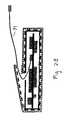
- FIG. 1is a schematic side sectional view of a prior art sensor.
- FIG. 2Ais a schematic side sectional view of a sensor according to an exemplary embodiment of the present invention.
- FIG. 2Bis a schematic side sectional view of a sensor according to an exemplary embodiment of the present invention.
- FIG. 3Ais a schematic showing an exemplary sensor according to the present invention in an unwrapped and a wrapped state.
- FIG. 3Bis a schematic showing an exemplary sensor of the present invention in an unwrapped and a wrapped state.
- FIG. 4Ais a bottom view of an exemplary sensor according to the present invention.
- FIG. 4Bis a top view of an exemplary sensor according to the present invention.
- FIG. 5is a schematic side sectional view of a sensor according to an exemplary embodiment of the present invention.
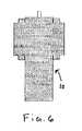
- FIG. 6is a top view of an exemplary sensor according to the present invention.
- FIG. 1is a schematic diagram of a prior art tamper respondent enclosure.
- Circuit board 100has components 101 disposed thereon. Components 101 contain the sensitive information that is desired to be protected.
- a box or enclosure 102surrounds circuit board 100 and components 101 .
- Enclosure 102has a sensor 103 disposed around it.
- Sensor 103comprises a clear PET substrate 104 .
- On both sides of PET substrate 104are disposed printed traces 105 . This is a matrix of conductive lines on each side. The lines are disposed in offsetting relation from one side to the other to ensure complete coverage of PET substrate 104 .
- the inside of PET substrate 104also has a layer of adhesive 106 disposed over the printed trace 105 on that surface.
- Adhesive layer 106is a pressure sensitive adhesive (PSA).
- PSApressure sensitive adhesive
- the entire sensoris then encapsulated in an opaque encapsulant or potting material 107 .
- Potting material 107helps obfuscate printed traces 105 .
- An outer shell 108surrounds the device.
- a cable 109is used to connect components 101 with exterior components 110 .
- the top section of sensor 103is shown to be open, this is for illustration purposes only. In use, the overlapping ends of sensor 103 are secured to one another by adhesive layer 106 .
- this deviceincludes the deposition of printed traces on two sides of the PET substrate and it also includes the potting layer 107 .
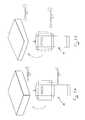
- FIG. 2Ais a schematic representation of an exemplary embodiment of the present invention.
- a circuit board 20has components 21 disposed thereon. Components 21 contain sensitive information to be protected.
- circuit board 20can include wireless transmitters as components 21 .
- Circuit board 20 and components 21are enclosed by a box or enclosure 22 .
- Enclosure 22may be any shape. A rectangular shape is shown in this embodiment, but it may also be trapezoidal, wedge-shaped, or any other shape.
- Enclosure 22is encapsulated by tamper respondent sensor 10 .
- tamper respondent sensor 10may be wrapped around a circuit board without a preexisting box or enclosure, in which case a filler may be used to form a surface over the circuit board to which tamper respondent sensor 10 adheres.
- Tamper respondent sensor 10includes a substrate 11 .
- substrate 11an insulating material such as PET.
- substrate 11is opaque. By using an opaque PET for substrate 11 , it is not necessary to subsequently pot the material in order to obfuscate the printed traces.
- Substrate 11has a first side 12 and second side 13 .
- First side 12is the inside of the substrate as illustrated in FIG. 2A .
- Disposed on this first side 12is a first layer of conductive traces 14 .
- the conductive tracesare made of a conductive, non-metallic ink, such as carbon-loaded polymer resin as taught, for example, in U.S. Pat. No. 5,539,379. Other materials known in the art may be used for the traces.
- Substrate 11is adapted to be folded to produce an overlapping portion of first side 12 with an overlapping portion of second side 13 .
- second side 13which is the outer side of substrate 11 in the illustrated embodiment, a second layer of conductive traces 15 is disposed.
- Second layer of conductive traces 15is present, however, only at the overlapping portion of second side 13 . That is, second layer of conductive traces 15 is only disposed on that portion of second side 13 where there is an overlap with first side 12 .
- the remainder of second side 13is a region free of conductive traces. Thus, there are no exposed traces on second side 13 .
- the traces on second side 13are electrically connected to the traces on first side 12 , for example by a via.
- the viasare located at the overlapping portion.
- a monitor(not shown) detects the circuit completed by first layer of conductive traces 14 and second layer of conductive traces 15 and monitors the electrical state. If this electrical state changes, indicating that the circuit has been broken, for example by cutting one of the traces, the monitor can trigger a response such as erasing information stored in components 21 .
- the overlap regionis open for purposes of illustration.
- the overlapis mated such that second layer of conductive traces 15 is adhered to first layer of conductive traces 14 by an adhesive layer 30 .
- Adhesive layer 30is preferably a tackifier, such as a PSA.
- Adhesive layer 30is disposed on first side 12 of substrate 11 on the first layer of conductive traces 14 .
- adhesive layer 30will sever either first layer of conductive traces 14 or second layer of conductive traces 15 , thereby causing an interruption in the signal and triggering erasure or other protection of information stored in components 21 as described above.
- a cable 71is used to connect components inside the device to components outside the device.
- FIG. 3A and FIG. 3Bshow alternative embodiments of the present invention.
- the embodimentsrepresents a sensor 10 for use in wrapping an enclosure of a rectangular shape ( FIG. 3A ) and a wedge shape ( FIG. 3B ).
- the portion of FIGS. 3A and 3B labeled “unwrapped”shows sensor 10 in its intermediate form. Once an enclosure is placed on sensor 10 , sensor 10 is then wrapped around the enclosure to completely encapsulate it, as illustrated in the portion of the figures labeled “wrapped.”
- FIG. 4Ais a bottom view of an exemplary sensor 10 according to the present invention.
- FIG. 4Bis a top view of sensor 10 .
- sensor 10includes substrate 11 .
- substrate 11is an opaque film such as PET.
- First side 12 of substrate 11has first layer of conductive traces 14 disposed thereon.
- traces 14are disposed in an unpredictable pattern on substrate 11 .
- Thisis in contrast to diagonal (zig-zag), straight, or sinusoidal wave trace lines known in the art. Because these known patterns repeat at regular intervals, it potentially makes the sensor vulnerable to a jumper attack wherein the attacker can locate two points of the same trace and bypass the trace with a conductive jumper. Potentially, the attacker can then penetrate the sensor without triggering a change in electrical state.
- the traceis more difficult to break into sensor 10 because it is difficult to follow a single conductive trace and bypass it with a jumper.
- the traceherein is manually drawn using computer-aided software packages such as PCB-PADS®, from Mentor Graphics, a printed circuit board layout software program.
- a second layer of conductive traces 15is disposed on the portions of second side 13 of substrate 11 that will overlap with first side 12 as described above.
- the remainder of second side 13is a region free of conductive traces. Thus, there are no exposed traces on second side 13 once it is wrapped around an enclosure.
- FIGS. 4A and 4BAlso shown in FIGS. 4A and 4B is an opening 20 in sensor 10 which is preferably included in sensor 10 to allow mating of a circuit board 20 with another device external to sensor 10 .
- the external devicecan be a computer mother board, a connector, or a cable, for example.
- FIG. 5illustrates an exemplary embodiment wherein opening 20 allows mating of component 21 to a connector 80 .
- FIGS. 4A and 4Bis an I/O lead 40 extending from substrate 11 .
- FIG. 6is a top view of exemplary sensor 10 without opening 20 . This sensor 10 of FIG. 6 would be connected using a cable through the overlap zone as shown in FIG. 2B .
- the present inventionprovides distinctive advantages over the known art. Specifically, employing an unpredictable pattern for the traces makes it more difficult to defeat the device. In addition, using an opaque PET for substrate 11 obviates the need to pot the sensor. This eliminates a processing step, making production more efficient and cost effective. It also provides natural obfuscation for the conductive traces which may render the use of a second layer of conductive traces over the entire second side 13 of substrate 11 unnecessary. This also eliminates processing steps increasing efficiency and reducing costs. By selectively putting the second layer of conductive traces 15 only at portions of the second side 13 where substrate 11 overlaps, an effective tamper respondent enclosure is produced.
- relatively small overlapping portionsare depicted.
- larger overlapping portionsare used, for example covering an entire side of box 22 or furthermore all sides of a box.
Landscapes
- Engineering & Computer Science (AREA)
- Computer Hardware Design (AREA)
- Microelectronics & Electronic Packaging (AREA)
- Computer Security & Cryptography (AREA)
- Physics & Mathematics (AREA)
- General Engineering & Computer Science (AREA)
- General Physics & Mathematics (AREA)
- Theoretical Computer Science (AREA)
- Software Systems (AREA)
- Structure Of Printed Boards (AREA)
- Burglar Alarm Systems (AREA)
- Measurement Of The Respiration, Hearing Ability, Form, And Blood Characteristics Of Living Organisms (AREA)
Abstract
Description
Claims (25)
Priority Applications (4)
| Application Number | Priority Date | Filing Date | Title |
|---|---|---|---|
| US11/592,766US7760086B2 (en) | 2006-11-03 | 2006-11-03 | Tamper respondent sensor and enclosure |
| JP2009535264AJP5600007B2 (en) | 2006-11-03 | 2007-10-11 | Unauthorized opening reaction type sensor and unauthorized opening reaction type enclosure |
| PCT/US2007/021881WO2008063320A2 (en) | 2006-11-03 | 2007-10-11 | Tamper respondent sensor and enclosure |
| EP07852722.3AEP2078208B1 (en) | 2006-11-03 | 2007-10-11 | Tamper respondent sensor and enclosure |
Applications Claiming Priority (1)
| Application Number | Priority Date | Filing Date | Title |
|---|---|---|---|
| US11/592,766US7760086B2 (en) | 2006-11-03 | 2006-11-03 | Tamper respondent sensor and enclosure |
Publications (2)
| Publication Number | Publication Date |
|---|---|
| US20080106400A1 US20080106400A1 (en) | 2008-05-08 |
| US7760086B2true US7760086B2 (en) | 2010-07-20 |
Family
ID=39359265
Family Applications (1)
| Application Number | Title | Priority Date | Filing Date |
|---|---|---|---|
| US11/592,766Expired - Fee RelatedUS7760086B2 (en) | 2006-11-03 | 2006-11-03 | Tamper respondent sensor and enclosure |
Country Status (4)
| Country | Link |
|---|---|
| US (1) | US7760086B2 (en) |
| EP (1) | EP2078208B1 (en) |
| JP (1) | JP5600007B2 (en) |
| WO (1) | WO2008063320A2 (en) |
Cited By (38)
| Publication number | Priority date | Publication date | Assignee | Title |
|---|---|---|---|---|
| US20080284610A1 (en)* | 2004-04-08 | 2008-11-20 | W.L. Gore & Associates (Uk) Limited | Tamper Respondent Enclosure |
| US8399781B1 (en)* | 2005-10-18 | 2013-03-19 | Teledyne Technologies Incorporated | Anti-tamper mesh |
| US20150163933A1 (en)* | 2013-12-09 | 2015-06-11 | Timothy Wayne Steiner | Tamper respondent apparatus |
| US9392734B1 (en) | 2014-02-11 | 2016-07-12 | Lockheed Martin Corporation | Security wrapper for an electronic assembly and methods for forming such a wrapper |
| US9554477B1 (en) | 2015-12-18 | 2017-01-24 | International Business Machines Corporation | Tamper-respondent assemblies with enclosure-to-board protection |
| US9560737B2 (en) | 2015-03-04 | 2017-01-31 | International Business Machines Corporation | Electronic package with heat transfer element(s) |
| US9555606B1 (en) | 2015-12-09 | 2017-01-31 | International Business Machines Corporation | Applying pressure to adhesive using CTE mismatch between components |
| US9578764B1 (en) | 2015-09-25 | 2017-02-21 | International Business Machines Corporation | Enclosure with inner tamper-respondent sensor(s) and physical security element(s) |
| US9591776B1 (en) | 2015-09-25 | 2017-03-07 | International Business Machines Corporation | Enclosure with inner tamper-respondent sensor(s) |
| US20170094778A1 (en)* | 2015-09-25 | 2017-03-30 | International Business Machines Corporation | Tamper-respondent assemblies with bond protection |
| US9858776B1 (en) | 2016-06-28 | 2018-01-02 | International Business Machines Corporation | Tamper-respondent assembly with nonlinearity monitoring |
| US9881880B2 (en) | 2016-05-13 | 2018-01-30 | International Business Machines Corporation | Tamper-proof electronic packages with stressed glass component substrate(s) |
| US9887847B2 (en) | 2016-02-03 | 2018-02-06 | International Business Machines Corporation | Secure crypto module including conductor on glass security layer |
| US9904811B2 (en) | 2016-04-27 | 2018-02-27 | International Business Machines Corporation | Tamper-proof electronic packages with two-phase dielectric fluid |
| US9913370B2 (en) | 2016-05-13 | 2018-03-06 | International Business Machines Corporation | Tamper-proof electronic packages formed with stressed glass |
| US9913389B2 (en)* | 2015-12-01 | 2018-03-06 | International Business Corporation Corporation | Tamper-respondent assembly with vent structure |
| US9911012B2 (en) | 2015-09-25 | 2018-03-06 | International Business Machines Corporation | Overlapping, discrete tamper-respondent sensors |
| US9916744B2 (en) | 2016-02-25 | 2018-03-13 | International Business Machines Corporation | Multi-layer stack with embedded tamper-detect protection |
| US9924591B2 (en) | 2015-09-25 | 2018-03-20 | International Business Machines Corporation | Tamper-respondent assemblies |
| US9978231B2 (en) | 2015-10-21 | 2018-05-22 | International Business Machines Corporation | Tamper-respondent assembly with protective wrap(s) over tamper-respondent sensor(s) |
| US9999124B2 (en) | 2016-11-02 | 2018-06-12 | International Business Machines Corporation | Tamper-respondent assemblies with trace regions of increased susceptibility to breaking |
| US10098235B2 (en) | 2015-09-25 | 2018-10-09 | International Business Machines Corporation | Tamper-respondent assemblies with region(s) of increased susceptibility to damage |
| US10136519B2 (en) | 2015-10-19 | 2018-11-20 | International Business Machines Corporation | Circuit layouts of tamper-respondent sensors |
| US10157527B1 (en) | 2017-11-28 | 2018-12-18 | International Business Machines Corporation | Embossed printed circuit board for intrusion detection |
| US10168185B2 (en) | 2015-09-25 | 2019-01-01 | International Business Machines Corporation | Circuit boards and electronic packages with embedded tamper-respondent sensor |
| US10172239B2 (en) | 2015-09-25 | 2019-01-01 | International Business Machines Corporation | Tamper-respondent sensors with formed flexible layer(s) |
| US10271424B2 (en) | 2016-09-26 | 2019-04-23 | International Business Machines Corporation | Tamper-respondent assemblies with in situ vent structure(s) |
| US10299372B2 (en) | 2016-09-26 | 2019-05-21 | International Business Machines Corporation | Vented tamper-respondent assemblies |
| US10306753B1 (en) | 2018-02-22 | 2019-05-28 | International Business Machines Corporation | Enclosure-to-board interface with tamper-detect circuit(s) |
| US10321589B2 (en) | 2016-09-19 | 2019-06-11 | International Business Machines Corporation | Tamper-respondent assembly with sensor connection adapter |
| US10327329B2 (en) | 2017-02-13 | 2019-06-18 | International Business Machines Corporation | Tamper-respondent assembly with flexible tamper-detect sensor(s) overlying in-situ-formed tamper-detect sensor |
| US10327343B2 (en) | 2015-12-09 | 2019-06-18 | International Business Machines Corporation | Applying pressure to adhesive using CTE mismatch between components |
| US10426037B2 (en) | 2015-07-15 | 2019-09-24 | International Business Machines Corporation | Circuitized structure with 3-dimensional configuration |
| US10579833B1 (en) | 2014-12-16 | 2020-03-03 | Thales Esecurity, Inc. | Tamper detection circuit assemblies and related manufacturing processes |
| US11089675B2 (en) | 2018-10-22 | 2021-08-10 | Te Connectivity Corporation | Tamper sensor |
| US11122682B2 (en) | 2018-04-04 | 2021-09-14 | International Business Machines Corporation | Tamper-respondent sensors with liquid crystal polymer layers |
| US11191154B2 (en) | 2018-06-13 | 2021-11-30 | International Business Machines Corporation | Enclosure with tamper respondent sensor |
| US20240069610A1 (en)* | 2022-08-31 | 2024-02-29 | Wiwynn Corporation | Server and storage module |
Families Citing this family (15)
| Publication number | Priority date | Publication date | Assignee | Title |
|---|---|---|---|---|
| WO2003085729A1 (en) | 2002-04-11 | 2003-10-16 | Koninklijke Philips Electronics N.V. | Method of manufacturing an electronic device |
| FR2933798A1 (en)* | 2008-07-11 | 2010-01-15 | Pierre Jean Merce | SECURITY DEVICE FOR MONITORING ACCESSIBILITY TO AN OBJECT |
| DE102009002559A1 (en)* | 2009-04-22 | 2010-10-28 | Robert Bosch Gmbh | sensor arrangement |
| US20130265163A1 (en)* | 2010-06-09 | 2013-10-10 | Raytheon Company | Magnetic Field Activated Intrusion Detection |
| AU2012220340A1 (en)* | 2011-02-22 | 2013-08-22 | Joelmar Pty Ltd | Survival and location enhancement garment and headgear |
| GB2504478A (en)* | 2012-07-27 | 2014-02-05 | Johnson Electric Sa | Security Wrap Film for Protecting Electronic Device |
| GB2515996A (en)* | 2013-04-15 | 2015-01-14 | Johnson Electric Sa | Security wrap with tearable substrate |
| JP6327054B2 (en)* | 2014-01-08 | 2018-05-23 | セイコーエプソン株式会社 | Fiscal printer |
| DE102015122000B4 (en)* | 2015-12-16 | 2019-02-07 | Fujitsu Client Computing Limited | Arrangement and electronic device |
| JP6613955B2 (en)* | 2016-02-26 | 2019-12-04 | 沖電気工業株式会社 | Input device and automatic transaction device |
| CN108260280B (en)* | 2017-12-04 | 2020-12-01 | 深圳市新宇腾跃电子有限公司 | FPC bending forming process |
| EP3550466B1 (en) | 2018-04-06 | 2023-08-02 | Fraunhofer-Gesellschaft zur Förderung der angewandten Forschung e.V. | Puf-film and method for producing the same |
| EP3550623B1 (en) | 2018-04-06 | 2020-07-29 | Fraunhofer-Gesellschaft zur Förderung der angewandten Forschung e.V. | Puf-film and method for producing the same |
| EP3550475A1 (en) | 2018-04-06 | 2019-10-09 | Fraunhofer-Gesellschaft zur Förderung der angewandten Forschung e.V. | Puf-film and method for producing the same |
| WO2022104099A1 (en)* | 2020-11-12 | 2022-05-19 | Jumbe Nelson L | Transducers, their methods of manufacture and uses |
Citations (31)
| Publication number | Priority date | Publication date | Assignee | Title |
|---|---|---|---|---|
| US3644825A (en) | 1969-12-31 | 1972-02-22 | Texas Instruments Inc | Magnetic detection system for detecting movement of an object utilizing signals derived from two orthogonal pickup coils |
| US4188549A (en) | 1977-11-11 | 1980-02-12 | Federal Screw Works | Acoustically responsive sensor switch |
| US4325089A (en) | 1979-12-10 | 1982-04-13 | Hsu Da L | System for safeguarding magnetically recorded data |
| US4593384A (en) | 1984-12-21 | 1986-06-03 | Ncr Corporation | Security device for the secure storage of sensitive data |
| GB2220513A (en) | 1988-06-17 | 1990-01-10 | Gore & Ass | Security enclosure |
| GB2256956A (en) | 1991-06-21 | 1992-12-23 | Gore & Ass | Security enclosures |
| GB2256957A (en) | 1991-06-21 | 1992-12-23 | Gore & Ass | Security enclosures |
| GB2256958A (en) | 1991-06-21 | 1992-12-23 | Gore & Ass | Security enclosures |
| GB2258075A (en) | 1991-07-24 | 1993-01-27 | Gore & Ass | Security enclosures |
| GB2270785A (en) | 1992-09-22 | 1994-03-23 | Gore & Ass | Security enclosure manufacture. |
| US5832772A (en) | 1995-01-27 | 1998-11-10 | The Regents Of The University Of California | Micropower RF material proximity sensor |
| US5858500A (en) | 1993-03-12 | 1999-01-12 | W. L. Gore & Associates, Inc. | Tamper respondent enclosure |
| DE19738990A1 (en) | 1997-09-05 | 1999-03-11 | Siemens Ag | Misuse protection device for chip card security system |
| WO1999021142A1 (en) | 1997-10-17 | 1999-04-29 | W. L. Gore & Associates (Uk) Limited | Tamper respondent enclosure |
| US5910774A (en) | 1996-09-18 | 1999-06-08 | Itron, Inc. | Sensor for count and tamper detection |
| GB2356276A (en) | 1999-09-13 | 2001-05-16 | Geneticware Co Ltd | Security mechanism for an integrated circuit packing box |
| FR2801999A1 (en) | 1999-12-01 | 2001-06-08 | Gemplus Card Int | Smart card with integrated circuit chips includes additional conductive mesh providing protection against fraudulent access to chips |
| WO2001059544A2 (en) | 2000-02-14 | 2001-08-16 | Rainbow Technologies B.V., Netherlands | Security module system, apparatus and process |
| US6396400B1 (en) | 1999-07-26 | 2002-05-28 | Epstein, Iii Edwin A. | Security system and enclosure to protect data contained therein |
| US6400268B1 (en) | 1992-05-10 | 2002-06-04 | Kjell Lindskog | Electrical manually portable security case for the storage of theft attractive articles with an electrical mat having at least one elongated electrically conductive wire in a substantially continuous mesh, loop or eye structure |
| US20020092672A1 (en) | 2001-01-16 | 2002-07-18 | Primavera Anthony A. | Contact pads and circuit boards incorporating same |
| US20020171439A1 (en) | 2001-05-21 | 2002-11-21 | Atsushi Ono | Electrostatic capacitance sensor |
| US6496119B1 (en) | 1998-11-05 | 2002-12-17 | Infineon Technologies Ag | Protection circuit for an integrated circuit |
| US6606123B2 (en) | 1999-01-29 | 2003-08-12 | Hamamatsu Photonics K.K. | Photosensitive device |
| US6686539B2 (en)* | 2001-01-03 | 2004-02-03 | International Business Machines Corporation | Tamper-responding encapsulated enclosure having flexible protective mesh structure |
| EP1462907A1 (en) | 2003-03-25 | 2004-09-29 | Bourns, Inc. | A security enclosure for a circuit |
| WO2005098950A1 (en) | 2004-04-08 | 2005-10-20 | W.L. Gore & Associates (Uk) Limited | Tamper respondent covering |
| US6982642B1 (en)* | 2000-11-20 | 2006-01-03 | International Business Machines Corporation | Security cloth design and assembly |
| US6996953B2 (en)* | 2004-01-23 | 2006-02-14 | Pitney Bowes Inc. | System and method for installing a tamper barrier wrap in a PCB assembly, including a PCB assembly having improved heat sinking |
| US20060049941A1 (en) | 2004-09-03 | 2006-03-09 | Hunter Steve B | Reusable tamper respondent enclosure |
| US20060163349A1 (en) | 2004-09-30 | 2006-07-27 | W5 Networks, Inc. | Wireless systems suitable for retail automation and promotion |
Family Cites Families (3)
| Publication number | Priority date | Publication date | Assignee | Title |
|---|---|---|---|---|
| JP2002049317A (en)* | 2000-05-23 | 2002-02-15 | Teikoku Tsushin Kogyo Co Ltd | Electrical peeling detection sheet |
| JP4580568B2 (en)* | 2001-02-09 | 2010-11-17 | 大日本印刷株式会社 | Storage box with non-contact IC tag |
| CA2409624C (en)* | 2002-10-25 | 2011-03-29 | Intelligent Devices Inc. | Electronic tampering detection system |
- 2006
- 2006-11-03USUS11/592,766patent/US7760086B2/ennot_activeExpired - Fee Related
- 2007
- 2007-10-11EPEP07852722.3Apatent/EP2078208B1/ennot_activeNot-in-force
- 2007-10-11JPJP2009535264Apatent/JP5600007B2/ennot_activeExpired - Fee Related
- 2007-10-11WOPCT/US2007/021881patent/WO2008063320A2/enactiveApplication Filing
Patent Citations (33)
| Publication number | Priority date | Publication date | Assignee | Title |
|---|---|---|---|---|
| US3644825A (en) | 1969-12-31 | 1972-02-22 | Texas Instruments Inc | Magnetic detection system for detecting movement of an object utilizing signals derived from two orthogonal pickup coils |
| US4188549A (en) | 1977-11-11 | 1980-02-12 | Federal Screw Works | Acoustically responsive sensor switch |
| US4325089A (en) | 1979-12-10 | 1982-04-13 | Hsu Da L | System for safeguarding magnetically recorded data |
| US4593384A (en) | 1984-12-21 | 1986-06-03 | Ncr Corporation | Security device for the secure storage of sensitive data |
| GB2220513A (en) | 1988-06-17 | 1990-01-10 | Gore & Ass | Security enclosure |
| GB2256956A (en) | 1991-06-21 | 1992-12-23 | Gore & Ass | Security enclosures |
| GB2256957A (en) | 1991-06-21 | 1992-12-23 | Gore & Ass | Security enclosures |
| GB2256958A (en) | 1991-06-21 | 1992-12-23 | Gore & Ass | Security enclosures |
| GB2258075A (en) | 1991-07-24 | 1993-01-27 | Gore & Ass | Security enclosures |
| US6400268B1 (en) | 1992-05-10 | 2002-06-04 | Kjell Lindskog | Electrical manually portable security case for the storage of theft attractive articles with an electrical mat having at least one elongated electrically conductive wire in a substantially continuous mesh, loop or eye structure |
| GB2270785A (en) | 1992-09-22 | 1994-03-23 | Gore & Ass | Security enclosure manufacture. |
| US5858500A (en) | 1993-03-12 | 1999-01-12 | W. L. Gore & Associates, Inc. | Tamper respondent enclosure |
| US5832772A (en) | 1995-01-27 | 1998-11-10 | The Regents Of The University Of California | Micropower RF material proximity sensor |
| US5910774A (en) | 1996-09-18 | 1999-06-08 | Itron, Inc. | Sensor for count and tamper detection |
| DE19738990A1 (en) | 1997-09-05 | 1999-03-11 | Siemens Ag | Misuse protection device for chip card security system |
| WO1999021142A1 (en) | 1997-10-17 | 1999-04-29 | W. L. Gore & Associates (Uk) Limited | Tamper respondent enclosure |
| US6496119B1 (en) | 1998-11-05 | 2002-12-17 | Infineon Technologies Ag | Protection circuit for an integrated circuit |
| US6606123B2 (en) | 1999-01-29 | 2003-08-12 | Hamamatsu Photonics K.K. | Photosensitive device |
| US6396400B1 (en) | 1999-07-26 | 2002-05-28 | Epstein, Iii Edwin A. | Security system and enclosure to protect data contained therein |
| GB2356276A (en) | 1999-09-13 | 2001-05-16 | Geneticware Co Ltd | Security mechanism for an integrated circuit packing box |
| FR2801999A1 (en) | 1999-12-01 | 2001-06-08 | Gemplus Card Int | Smart card with integrated circuit chips includes additional conductive mesh providing protection against fraudulent access to chips |
| WO2001059544A2 (en) | 2000-02-14 | 2001-08-16 | Rainbow Technologies B.V., Netherlands | Security module system, apparatus and process |
| US20020002683A1 (en) | 2000-02-14 | 2002-01-03 | Benson Justin H. | Security module system, apparatus and process |
| US7054162B2 (en)* | 2000-02-14 | 2006-05-30 | Safenet, Inc. | Security module system, apparatus and process |
| US6982642B1 (en)* | 2000-11-20 | 2006-01-03 | International Business Machines Corporation | Security cloth design and assembly |
| US6686539B2 (en)* | 2001-01-03 | 2004-02-03 | International Business Machines Corporation | Tamper-responding encapsulated enclosure having flexible protective mesh structure |
| US20020092672A1 (en) | 2001-01-16 | 2002-07-18 | Primavera Anthony A. | Contact pads and circuit boards incorporating same |
| US20020171439A1 (en) | 2001-05-21 | 2002-11-21 | Atsushi Ono | Electrostatic capacitance sensor |
| EP1462907A1 (en) | 2003-03-25 | 2004-09-29 | Bourns, Inc. | A security enclosure for a circuit |
| US6996953B2 (en)* | 2004-01-23 | 2006-02-14 | Pitney Bowes Inc. | System and method for installing a tamper barrier wrap in a PCB assembly, including a PCB assembly having improved heat sinking |
| WO2005098950A1 (en) | 2004-04-08 | 2005-10-20 | W.L. Gore & Associates (Uk) Limited | Tamper respondent covering |
| US20060049941A1 (en) | 2004-09-03 | 2006-03-09 | Hunter Steve B | Reusable tamper respondent enclosure |
| US20060163349A1 (en) | 2004-09-30 | 2006-07-27 | W5 Networks, Inc. | Wireless systems suitable for retail automation and promotion |
Cited By (81)
| Publication number | Priority date | Publication date | Assignee | Title |
|---|---|---|---|---|
| US7978070B2 (en)* | 2004-04-08 | 2011-07-12 | W. L. Gore & Associates (Uk) Ltd. | Tamper respondent enclosure |
| US20080284610A1 (en)* | 2004-04-08 | 2008-11-20 | W.L. Gore & Associates (Uk) Limited | Tamper Respondent Enclosure |
| US8399781B1 (en)* | 2005-10-18 | 2013-03-19 | Teledyne Technologies Incorporated | Anti-tamper mesh |
| US20150163933A1 (en)* | 2013-12-09 | 2015-06-11 | Timothy Wayne Steiner | Tamper respondent apparatus |
| US9521764B2 (en)* | 2013-12-09 | 2016-12-13 | Timothy Steiner | Tamper respondent apparatus |
| US9392734B1 (en) | 2014-02-11 | 2016-07-12 | Lockheed Martin Corporation | Security wrapper for an electronic assembly and methods for forming such a wrapper |
| US11250171B1 (en) | 2014-12-16 | 2022-02-15 | Thales Esecurity, Inc. | Three-dimensional (3D) printing of a tamper sensor assembly |
| US10579833B1 (en) | 2014-12-16 | 2020-03-03 | Thales Esecurity, Inc. | Tamper detection circuit assemblies and related manufacturing processes |
| US10237964B2 (en) | 2015-03-04 | 2019-03-19 | International Business Machines Corporation | Manufacturing electronic package with heat transfer element(s) |
| US9560737B2 (en) | 2015-03-04 | 2017-01-31 | International Business Machines Corporation | Electronic package with heat transfer element(s) |
| US10426037B2 (en) | 2015-07-15 | 2019-09-24 | International Business Machines Corporation | Circuitized structure with 3-dimensional configuration |
| US10524362B2 (en) | 2015-07-15 | 2019-12-31 | International Business Machines Corporation | Circuitized structure with 3-dimensional configuration |
| US9911012B2 (en) | 2015-09-25 | 2018-03-06 | International Business Machines Corporation | Overlapping, discrete tamper-respondent sensors |
| US10098235B2 (en) | 2015-09-25 | 2018-10-09 | International Business Machines Corporation | Tamper-respondent assemblies with region(s) of increased susceptibility to damage |
| US10271434B2 (en) | 2015-09-25 | 2019-04-23 | International Business Machines Corporation | Method of fabricating a tamper-respondent assembly with region(s) of increased susceptibility to damage |
| US10257939B2 (en) | 2015-09-25 | 2019-04-09 | International Business Machines Corporation | Method of fabricating tamper-respondent sensor |
| US10331915B2 (en) | 2015-09-25 | 2019-06-25 | International Business Machines Corporation | Overlapping, discrete tamper-respondent sensors |
| US10178818B2 (en) | 2015-09-25 | 2019-01-08 | International Business Machines Corporation | Enclosure with inner tamper-respondent sensor(s) and physical security element(s) |
| US9894749B2 (en)* | 2015-09-25 | 2018-02-13 | International Business Machines Corporation | Tamper-respondent assemblies with bond protection |
| US10685146B2 (en) | 2015-09-25 | 2020-06-16 | International Business Machines Corporation | Overlapping, discrete tamper-respondent sensors |
| US10624202B2 (en) | 2015-09-25 | 2020-04-14 | International Business Machines Corporation | Tamper-respondent assemblies with bond protection |
| US9913416B2 (en) | 2015-09-25 | 2018-03-06 | International Business Machines Corporation | Enclosure with inner tamper-respondent sensor(s) and physical security element(s) |
| US9913362B2 (en) | 2015-09-25 | 2018-03-06 | International Business Machines Corporation | Tamper-respondent assemblies with bond protection |
| US10334722B2 (en) | 2015-09-25 | 2019-06-25 | International Business Machines Corporation | Tamper-respondent assemblies |
| US10264665B2 (en) | 2015-09-25 | 2019-04-16 | International Business Machines Corporation | Tamper-respondent assemblies with bond protection |
| US20170094778A1 (en)* | 2015-09-25 | 2017-03-30 | International Business Machines Corporation | Tamper-respondent assemblies with bond protection |
| US9924591B2 (en) | 2015-09-25 | 2018-03-20 | International Business Machines Corporation | Tamper-respondent assemblies |
| US9936573B2 (en) | 2015-09-25 | 2018-04-03 | International Business Machines Corporation | Tamper-respondent assemblies |
| US10175064B2 (en) | 2015-09-25 | 2019-01-08 | International Business Machines Corporation | Circuit boards and electronic packages with embedded tamper-respondent sensor |
| US10378925B2 (en) | 2015-09-25 | 2019-08-13 | International Business Machines Corporation | Circuit boards and electronic packages with embedded tamper-respondent sensor |
| US9591776B1 (en) | 2015-09-25 | 2017-03-07 | International Business Machines Corporation | Enclosure with inner tamper-respondent sensor(s) |
| US9717154B2 (en) | 2015-09-25 | 2017-07-25 | International Business Machines Corporation | Enclosure with inner tamper-respondent sensor(s) |
| US9578764B1 (en) | 2015-09-25 | 2017-02-21 | International Business Machines Corporation | Enclosure with inner tamper-respondent sensor(s) and physical security element(s) |
| US10172239B2 (en) | 2015-09-25 | 2019-01-01 | International Business Machines Corporation | Tamper-respondent sensors with formed flexible layer(s) |
| US10378924B2 (en) | 2015-09-25 | 2019-08-13 | International Business Machines Corporation | Circuit boards and electronic packages with embedded tamper-respondent sensor |
| US10395067B2 (en) | 2015-09-25 | 2019-08-27 | International Business Machines Corporation | Method of fabricating a tamper-respondent sensor assembly |
| US10168185B2 (en) | 2015-09-25 | 2019-01-01 | International Business Machines Corporation | Circuit boards and electronic packages with embedded tamper-respondent sensor |
| US10136519B2 (en) | 2015-10-19 | 2018-11-20 | International Business Machines Corporation | Circuit layouts of tamper-respondent sensors |
| US10143090B2 (en) | 2015-10-19 | 2018-11-27 | International Business Machines Corporation | Circuit layouts of tamper-respondent sensors |
| US9978231B2 (en) | 2015-10-21 | 2018-05-22 | International Business Machines Corporation | Tamper-respondent assembly with protective wrap(s) over tamper-respondent sensor(s) |
| US9913389B2 (en)* | 2015-12-01 | 2018-03-06 | International Business Corporation Corporation | Tamper-respondent assembly with vent structure |
| US20180110142A1 (en)* | 2015-12-01 | 2018-04-19 | International Business Machines Corporation | Tamper-respondent assembly with vent structure |
| US10251288B2 (en)* | 2015-12-01 | 2019-04-02 | International Business Machines Corporation | Tamper-respondent assembly with vent structure |
| US9555606B1 (en) | 2015-12-09 | 2017-01-31 | International Business Machines Corporation | Applying pressure to adhesive using CTE mismatch between components |
| US10327343B2 (en) | 2015-12-09 | 2019-06-18 | International Business Machines Corporation | Applying pressure to adhesive using CTE mismatch between components |
| US10172232B2 (en) | 2015-12-18 | 2019-01-01 | International Business Machines Corporation | Tamper-respondent assemblies with enclosure-to-board protection |
| US9554477B1 (en) | 2015-12-18 | 2017-01-24 | International Business Machines Corporation | Tamper-respondent assemblies with enclosure-to-board protection |
| US9877383B2 (en) | 2015-12-18 | 2018-01-23 | International Business Machines Corporation | Tamper-respondent assemblies with enclosure-to-board protection |
| US9661747B1 (en) | 2015-12-18 | 2017-05-23 | International Business Machines Corporation | Tamper-respondent assemblies with enclosure-to-board protection |
| US9887847B2 (en) | 2016-02-03 | 2018-02-06 | International Business Machines Corporation | Secure crypto module including conductor on glass security layer |
| US10715337B2 (en) | 2016-02-03 | 2020-07-14 | International Business Machines Corporation | Secure crypto module including conductor on glass security layer |
| US10169968B1 (en) | 2016-02-25 | 2019-01-01 | International Business Machines Corporation | Multi-layer stack with embedded tamper-detect protection |
| US10217336B2 (en) | 2016-02-25 | 2019-02-26 | International Business Machines Corporation | Multi-layer stack with embedded tamper-detect protection |
| US9916744B2 (en) | 2016-02-25 | 2018-03-13 | International Business Machines Corporation | Multi-layer stack with embedded tamper-detect protection |
| US10115275B2 (en) | 2016-02-25 | 2018-10-30 | International Business Machines Corporation | Multi-layer stack with embedded tamper-detect protection |
| US10169967B1 (en) | 2016-02-25 | 2019-01-01 | International Business Machines Corporation | Multi-layer stack with embedded tamper-detect protection |
| US9904811B2 (en) | 2016-04-27 | 2018-02-27 | International Business Machines Corporation | Tamper-proof electronic packages with two-phase dielectric fluid |
| US10169624B2 (en) | 2016-04-27 | 2019-01-01 | International Business Machines Corporation | Tamper-proof electronic packages with two-phase dielectric fluid |
| US9881880B2 (en) | 2016-05-13 | 2018-01-30 | International Business Machines Corporation | Tamper-proof electronic packages with stressed glass component substrate(s) |
| US10177102B2 (en) | 2016-05-13 | 2019-01-08 | International Business Machines Corporation | Tamper-proof electronic packages with stressed glass component substrate(s) |
| US9913370B2 (en) | 2016-05-13 | 2018-03-06 | International Business Machines Corporation | Tamper-proof electronic packages formed with stressed glass |
| US10257924B2 (en) | 2016-05-13 | 2019-04-09 | International Business Machines Corporation | Tamper-proof electronic packages formed with stressed glass |
| US10535619B2 (en) | 2016-05-13 | 2020-01-14 | International Business Machines Corporation | Tamper-proof electronic packages with stressed glass component substrate(s) |
| US10535618B2 (en) | 2016-05-13 | 2020-01-14 | International Business Machines Corporation | Tamper-proof electronic packages with stressed glass component substrate(s) |
| US9858776B1 (en) | 2016-06-28 | 2018-01-02 | International Business Machines Corporation | Tamper-respondent assembly with nonlinearity monitoring |
| US10242543B2 (en) | 2016-06-28 | 2019-03-26 | International Business Machines Corporation | Tamper-respondent assembly with nonlinearity monitoring |
| US10321589B2 (en) | 2016-09-19 | 2019-06-11 | International Business Machines Corporation | Tamper-respondent assembly with sensor connection adapter |
| US10299372B2 (en) | 2016-09-26 | 2019-05-21 | International Business Machines Corporation | Vented tamper-respondent assemblies |
| US10667389B2 (en) | 2016-09-26 | 2020-05-26 | International Business Machines Corporation | Vented tamper-respondent assemblies |
| US10271424B2 (en) | 2016-09-26 | 2019-04-23 | International Business Machines Corporation | Tamper-respondent assemblies with in situ vent structure(s) |
| US9999124B2 (en) | 2016-11-02 | 2018-06-12 | International Business Machines Corporation | Tamper-respondent assemblies with trace regions of increased susceptibility to breaking |
| US10327329B2 (en) | 2017-02-13 | 2019-06-18 | International Business Machines Corporation | Tamper-respondent assembly with flexible tamper-detect sensor(s) overlying in-situ-formed tamper-detect sensor |
| US10157527B1 (en) | 2017-11-28 | 2018-12-18 | International Business Machines Corporation | Embossed printed circuit board for intrusion detection |
| US10306753B1 (en) | 2018-02-22 | 2019-05-28 | International Business Machines Corporation | Enclosure-to-board interface with tamper-detect circuit(s) |
| US11083082B2 (en) | 2018-02-22 | 2021-08-03 | International Business Machines Corporation | Enclosure-to-board interface with tamper-detect circuit(s) |
| US10531561B2 (en) | 2018-02-22 | 2020-01-07 | International Business Machines Corporation | Enclosure-to-board interface with tamper-detect circuit(s) |
| US11122682B2 (en) | 2018-04-04 | 2021-09-14 | International Business Machines Corporation | Tamper-respondent sensors with liquid crystal polymer layers |
| US11191154B2 (en) | 2018-06-13 | 2021-11-30 | International Business Machines Corporation | Enclosure with tamper respondent sensor |
| US11089675B2 (en) | 2018-10-22 | 2021-08-10 | Te Connectivity Corporation | Tamper sensor |
| US20240069610A1 (en)* | 2022-08-31 | 2024-02-29 | Wiwynn Corporation | Server and storage module |
| US11934235B1 (en)* | 2022-08-31 | 2024-03-19 | Wiwynn Corporation | Server and storage module |
Also Published As
| Publication number | Publication date |
|---|---|
| WO2008063320A3 (en) | 2008-08-28 |
| EP2078208A4 (en) | 2010-11-03 |
| WO2008063320A2 (en) | 2008-05-29 |
| JP2010509655A (en) | 2010-03-25 |
| EP2078208B1 (en) | 2013-12-11 |
| EP2078208A2 (en) | 2009-07-15 |
| JP5600007B2 (en) | 2014-10-01 |
| US20080106400A1 (en) | 2008-05-08 |
Similar Documents
| Publication | Publication Date | Title |
|---|---|---|
| US7760086B2 (en) | Tamper respondent sensor and enclosure | |
| US10378925B2 (en) | Circuit boards and electronic packages with embedded tamper-respondent sensor | |
| US10251288B2 (en) | Tamper-respondent assembly with vent structure | |
| US10172232B2 (en) | Tamper-respondent assemblies with enclosure-to-board protection | |
| CN108027869B (en) | Tamper-respondent sensor with shaped flexible layer | |
| EP2186036B1 (en) | Tamper respondent system | |
| US9578764B1 (en) | Enclosure with inner tamper-respondent sensor(s) and physical security element(s) | |
| US11083082B2 (en) | Enclosure-to-board interface with tamper-detect circuit(s) | |
| EP1421549B1 (en) | A pin pad | |
| US20180103537A1 (en) | Tamper-respondent assemblies with bond protection | |
| US20180070444A1 (en) | Tamper-respondent assemblies | |
| US20170094805A1 (en) | Tamper-respondent assemblies with region(s) of increased susceptibility to damage | |
| JP2018531446A6 (en) | Tamper-open sensor with a formed flexible layer | |
| US9999124B2 (en) | Tamper-respondent assemblies with trace regions of increased susceptibility to breaking | |
| JP2010509655A5 (en) |
Legal Events
| Date | Code | Title | Description |
|---|---|---|---|
| AS | Assignment | Owner name:GORE ENTERPRISE HOLDINGS, INC., DELAWARE Free format text:ASSIGNMENT OF ASSIGNORS INTEREST;ASSIGNORS:HUNTER, STEVE B.;VOLTZ, JOHN A.;LEWIS, BRENT W.;AND OTHERS;REEL/FRAME:018840/0343;SIGNING DATES FROM 20070117 TO 20070119 Owner name:GORE ENTERPRISE HOLDINGS, INC., DELAWARE Free format text:ASSIGNMENT OF ASSIGNORS INTEREST;ASSIGNORS:HUNTER, STEVE B.;VOLTZ, JOHN A.;LEWIS, BRENT W.;AND OTHERS;SIGNING DATES FROM 20070117 TO 20070119;REEL/FRAME:018840/0343 | |
| STCF | Information on status: patent grant | Free format text:PATENTED CASE | |
| AS | Assignment | Owner name:W. L. GORE & ASSOCIATES, INC., DELAWARE Free format text:ASSIGNMENT OF ASSIGNORS INTEREST;ASSIGNOR:GORE ENTERPRISE HOLDINGS, INC.;REEL/FRAME:027906/0508 Effective date:20120130 | |
| FPAY | Fee payment | Year of fee payment:4 | |
| MAFP | Maintenance fee payment | Free format text:PAYMENT OF MAINTENANCE FEE, 8TH YEAR, LARGE ENTITY (ORIGINAL EVENT CODE: M1552) Year of fee payment:8 | |
| FEPP | Fee payment procedure | Free format text:MAINTENANCE FEE REMINDER MAILED (ORIGINAL EVENT CODE: REM.); ENTITY STATUS OF PATENT OWNER: LARGE ENTITY | |
| LAPS | Lapse for failure to pay maintenance fees | Free format text:PATENT EXPIRED FOR FAILURE TO PAY MAINTENANCE FEES (ORIGINAL EVENT CODE: EXP.); ENTITY STATUS OF PATENT OWNER: LARGE ENTITY | |
| STCH | Information on status: patent discontinuation | Free format text:PATENT EXPIRED DUE TO NONPAYMENT OF MAINTENANCE FEES UNDER 37 CFR 1.362 | |
| FP | Lapsed due to failure to pay maintenance fee | Effective date:20220720 |