US7759949B2 - Probes with self-cleaning blunt skates for contacting conductive pads - Google Patents
Probes with self-cleaning blunt skates for contacting conductive padsDownload PDFInfo
- Publication number
- US7759949B2 US7759949B2US11/480,302US48030206AUS7759949B2US 7759949 B2US7759949 B2US 7759949B2US 48030206 AUS48030206 AUS 48030206AUS 7759949 B2US7759949 B2US 7759949B2
- Authority
- US
- United States
- Prior art keywords
- skate
- probe
- tip
- radius
- curve
- Prior art date
- Legal status (The legal status is an assumption and is not a legal conclusion. Google has not performed a legal analysis and makes no representation as to the accuracy of the status listed.)
- Expired - Lifetime, expires
Links
Images


Classifications
- G—PHYSICS
- G01—MEASURING; TESTING
- G01R—MEASURING ELECTRIC VARIABLES; MEASURING MAGNETIC VARIABLES
- G01R1/00—Details of instruments or arrangements of the types included in groups G01R5/00 - G01R13/00 and G01R31/00
- G01R1/02—General constructional details
- G01R1/06—Measuring leads; Measuring probes
- G01R1/067—Measuring probes
- G01R1/06711—Probe needles; Cantilever beams; "Bump" contacts; Replaceable probe pins
- G01R1/06733—Geometry aspects
- G—PHYSICS
- G01—MEASURING; TESTING
- G01R—MEASURING ELECTRIC VARIABLES; MEASURING MAGNETIC VARIABLES
- G01R3/00—Apparatus or processes specially adapted for the manufacture or maintenance of measuring instruments, e.g. of probe tips
- G—PHYSICS
- G01—MEASURING; TESTING
- G01R—MEASURING ELECTRIC VARIABLES; MEASURING MAGNETIC VARIABLES
- G01R1/00—Details of instruments or arrangements of the types included in groups G01R5/00 - G01R13/00 and G01R31/00
- G01R1/02—General constructional details
- G01R1/06—Measuring leads; Measuring probes
- G01R1/067—Measuring probes
- G01R1/06711—Probe needles; Cantilever beams; "Bump" contacts; Replaceable probe pins
- G01R1/06733—Geometry aspects
- G01R1/06738—Geometry aspects related to tip portion
Definitions
- the present inventionrelates to cantilever probes.
- the present inventionrelates to a cantilever probe with angle fixture and a probe apparatus therewith.
- This inventionrelates generally to probes for testing devices under test (DUTs), and in particular to probes with contacting tips terminated in blunt skates to promote self-cleaning on contact with contacting pads as well as self-cleaning methods.
- cantilever probesare commonly fixed with their peripheral ends having their cantilever portion with the contacting tip freely suspended to provide the required flexibility.
- the fixture portion of the cantilever probeis commonly extensively dimensioned, which in turn consumes extensive real estate forcing multilayer cantilever probe assemblies with varying cantilever geometries.
- Such varying cantilever geometriesresult in different deflection behavior and limited average positioning accuracy of all cantilever probes of a probe apparatus.
- cantilever probes of the prior artare commonly fixed in a surrounding fashion along a linear fixture element, which requires additional surrounding referencing and/or positioning structures, which in turn consume additional space between the cantilever probes.
- Prior art cantilever probesare commonly fabricated with lengthy peripheral structures for a sufficient fanning out between the ever decreasing test contact pitches and circuit board contacts of the probe apparatus.
- Peripheral fan-out structuresmay be a multitude of the cantilever portion, which reduces the positioning accuracy of the ever decreasing cantilevers and contacting tips.
- cantilever probe and probe assemblythat provides maximum contacting tip accuracy together with homogeneous deflection behavior within a minimum footprint.
- cantilever probesmay be simple and highly consistent in geometry for inexpensive mass production.
- Other affiliated structures of the probe apparatusmay be inexpensively fabricated to accommodate for highly individualized probe apparatus configurations. Embodiments of the present invention address these needs.
- DUTsdevices under test
- chipsare getting smaller and they have more tightly spaced conductive pads.
- the padsare no longer located about the circuit perimeter, but in some designs may be found within the area occupied by the circuit itself.
- the density of leads carrying test signals to the padsis increasing.
- the pads themselvesare getting thinner and more susceptible to damage during a test. Meanwhile, the need to establish reliable electrical contact with each of the pads remains.
- a well-known prior art solution to establishing reliable electrical contact between a probe and a pad of a DUTinvolves the use of probes that execute a scrub motion on the pad.
- the scrub motionremoves the accumulated oxide layer and any dirt or debris that acts as an insulator and thus reduces contact resistance between the probe and the pad.
- U.S. Pat. No. 5,436,571 to KarasawaU.S. Pat. Nos. 5,773,987 and 6,433,571 both to Montoya
- this type of probecauses a knife edge and/or single point of contact effects to take place at the tip-pad interface. These effects can causes irreversible damage to pads, especially low-K conductive pads made of aluminum or soft metal. On the other hand, when insufficient contact force is applied between the probe tip and the pad, then the oxide and any debris at the probe-pad interface will not be efficiently removed.
- a still further object of the inventionis to provide probes and self-cleaning methods that can be applied in various probe geometries, probe cards and test arrangements.
- a cantilever probehas an elbow for bonding to a dual plane fixture plate having two substantially non parallel fixture surfaces in an angle corresponding to the elbow.
- the dual plane angled fixture between elbow and fixture plateprovides for a highly stiff and precise hold of the bonded cantilever probe with minimal real estate consumption.
- the cantilever probemay feature at least two positioning pins one of which may be placed at the contacting tip and the other one may extend from at least one of two contacting faces of the elbow.
- the elbow positioning pinmay fit into a corresponding elbow pin hole on one of the fixture surfaces.
- the tip positioning pinmay fit into a corresponding tip pin hole of a sacrificial assembly plate temporarily combined with the fixture plate for a precise positioning of the cantilever probes during curing, setting or hardening of a bonding agent between the fixture plate an the elbow. After assembly of a number of cantilever probes, the sacrificial plate may be removed and the tip pins eventually sanded to a common plane.
- Separate fan-out beamsmay be aligned with beam positioning pins on and attached to the fixture plate.
- the fan-out beamsare aligned and conductively connected with their probe connect ends to respective probe elbows once the cantilever probes are fixed.
- the fan-out beamsin turn may be conductively connected with their respective peripheral connect ends to well known large pitch apparatus terminals of a circuit board.
- Cantilever probes and fan-out beamsmay have geometries suitable for inexpensive mass fabrication by well known masked electro deposition fabrication techniques.
- a probe apparatusmay be easily customized by providing varying drill patterns of the positioning holes for fan-out beams and cantilever probes to match pitch requirements of the tested circuit chips.
- the objects and advantages of the inventionare secured by a probe designed for engaging a conductive pad of a device under test (DUT).
- the probehas an electrically conductive body that ends in a contacting tip of a certain tip width.
- At least one blunt skate that is narrower than the tip widthterminates the contacting tip.
- the blunt skateis aligned along a scrub direction and also has a certain curvature along the scrub direction to produce a self-cleaning rotation or rocking motion.
- the curvature of the blunt skateneeds to have an appropriate radius of curvature.
- the radius of curvatureis variable and decreasing towards the front of the skate. Since the skate is preferably symmetric about a midpoint, the same variable radius of curvature can be used in the back half of the skate.
- the cross-section of the blunt skateis flat and in another it has a rounded cross-section. In general, it is preferable that the skate have a width of less than 12 ⁇ m and a length of less than 75 ⁇ m. It should be noted that probes with blunt skates in this dimensional range are very well-suited for contacting DUTs with low-K conductive pads that are mechanically fragile.
- the probeis made of material layers. Such layers can be grown, e.g., in a deposition process.
- the blunt skatecan be formed from an extension of one of the material layers.
- the most appropriate material layer for forming a blunt skate from its extensionis a hard conductive material such as rhodium or cobalt.
- the skatescan be arranged parallel to each other. Alternatively, or in addition the skates can be staggered along the scrub direction.
- the inventionfurther extends to a method for engaging probes that have conductive bodies and contacting tips terminating in one or more blunt skates with a conductive pad.
- the skate or skatesare narrower than the tip width.
- the skate or skatesare provided with a curvature aligned along the scrub direction for producing the self-cleaning rotation.
- the application of a contact force between the skate and the conductive padcauses the skate to undergo a scrub motion along the scrub direction and a self-cleaning rotation that removes debris.
- the debrisis usually accumulated during previous engagements with or touch-downs on pads and its removal from the skate preserves low contact resistance.
- the contact forceis augmented to increase the self-cleaning rotation. This can be done whenever excess debris accumulates. Typically this will take place after several cycles, and thus the contact force can be augmented after two or more touch-down cycles to augment the self-cleaning rotation.
- a test current iis applied to the probe after applying the contact force. This means that the skate delivers the test current i to the pad after performing the scrub motion that removes any oxide from the pad and establishing electrical contact with it. Note that no current is applied when performing increased self-cleaning rotation of the skate. The same method is applied when two or more parallel and/or staggered skates are used.
- the probes of inventioncan be used in various apparatus and situations.
- the probescan be used in a probe card for testing devices under test (DUTs) such as semiconductor wafers.
- DUTsdevices under test
- the probe cardrequires appropriate design and devices, such as a source for delivering the test current i as well as arrangements for providing the overdrive to apply the contact force between the probes and the pads of the DUT.
- FIG. 1Ais a front view of an exemplary cantilever probe of the preferred embodiment parallel a symmetry plane of the cantilever probe.
- FIG. 1Bis a perspective view of the cantilever probe of FIG. 1A .
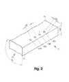
- FIG. 2is the perspective view of a first portion of a fixture plate including two fixture surfaces and elbow alignment holes.
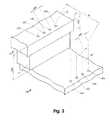
- FIG. 3is the perspective view of the fixture plate of FIG. 2 together with a sacrificial spacing structure and sacrificial assembly plate.
- FIG. 4is the perspective view of the plates of FIG. 3 with a number of assembled cantilever probes of FIGS. 1A , 1 B.
- FIG. 5is the perspective view of assembled probes and fixture plate of FIG. 4 with removed sacrificial spacing structure and sacrificial assembly plate.
- FIG. 6is the perspective view of a second portion of a fixture plate including the first portion of FIG. 2 and alignment holes for fan-out beams.
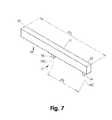
- FIG. 7is the perspective view of an exemplary fan-out beam.
- FIG. 8is the perspective view of the assembled cantilever probes and fixture plate of FIG. 5 , the fixture plate of FIG. 6 and a number of assembled fan-out beams of FIG. 7 conductively connected with respective cantilever probes.
- FIG. 9is a three-dimensional view of a portion of a probe card employing probes with blunt skates according to the invention.
- FIG. 10Ais a plan side view of a contacting tip of a single probe from FIG. 9 equipped with a blunt skate.
- FIG. 10Bis a front cross-sectional view of the contacting tip of the single probe from FIG. 9 .
- FIG. 11A-Dare three-dimensional views of the successive steps in engaging a blunt skate with a low-K conductive pad.
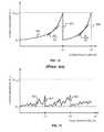
- FIG. 12(prior art) is a graph of contact resistance R c between a typical flat contacting tip and a conductive pad as a function of touch-down cycles.
- FIG. 13is a graph of contact resistance R c between a contacting tip equipped with a blunt skate in accordance with the invention and a conductive pad.
- FIG. 14is a diagram comparing the performance of a prior art chisel tip and a tip with a blunt skate in accordance with the invention.
- FIG. 15A-Dare three-dimensional views of alternative probe tips with one or more blunt skates according to the invention.
- FIG. 16A-Bare microscope images of a preferred blunt skate prior to use and after one million touch-down cycles.
- a cantilever probe 1 for test contacting a well known test contact of a tested electronic circuitry along a contacting axis CAmay have a tip positioning pin 14 configured for the test contacting.
- the tip positioning pin 14may also be configured for an aligning insertion in a respective one of tip pin holes 43 A- 43 N (see FIG. 3 ) also along the contacting axis CA.
- the cantilever probe 1may further feature a cantilever 13 for resiliently holding the tip positioning pin 14 with respect to the contacting axis CA with a predetermined deflection behavior including a well known scrub motion along the symmetry plane SP.
- a base arm 11may rigidly extend from said cantilever probe 13 such that operational deflection of the cantilever 13 leaves a base arm assembly face 111 substantially free of deformation.
- An offset arm 12extends substantially rigid from the base arm 11 in a substantially non parallel elbow angle AE defining together with the base arm 11 a fixture elbow 10 for rigidly fixing the cantilever probe 1 preferably via base arm assembly face 111 and offset arm assembly face 122 .
- An elbow positioning pin 15extends from one of the base arm 11 and the offset arm 12 along an elbow pin axis PA, which is substantially parallel to the contacting axis CA. The elbow positioning pin 15 is configured for an aligning insertion in a respective one of elbow pin holes 23 A- 23 N (see FIGS.
- the base arm assembly face 111has a length 111 L and the offset arm assembly face 121 has length 121 L.
- the contacting axis CAis in a probe pin distance AP to the elbow pin axis PA.
- the cantilever 13may preferably have a bend 131 terminating at the base arm 11 , which in turn may preferably extend substantially parallel to the contacting axis CA. In that case, the elbow positioning pin 14 may extend from the offset arm 12 .
- the cantilever 13 , the base arm 11 and the offset arm 12may have a continuously protruding profile perpendicular with respect to the symmetry plane SP and the contacting axis CA.
- the cantilever probe 1may be fabricated by a masked electro deposition process in which a central layer including the position pins 14 , 15 is interposed between profile layers.
- the positioning tips 14 , 15may have at least rectangular but preferably square cross section.
- the cantilever probe 1may consequently be also substantially symmetric with respect to the symmetry plane SP that coincides with the contacting axis CA and the elbow pin axis PA.
- Deflection behavior of the cantilever 13may be tuned by adjusting the cantilever length 13 L, cantilever height 13 H, profile width 1 W as well as shape and material composition of the cantilever 13 as may be well appreciated by anyone skilled in the art.
- another suspension structuremay be employed such as a suspension knee disclosed in the cross referenced US Application, titled “Freely Deflecting Knee Probe With Controlled Scrub Motion”.
- the tip positioning pinmay be combined with the suspension knee at the contacting face.
- a probe fixture plate 2 for fixedly holding a number of cantilever probes 1may have a first fixture surface 22 featuring a number of primary positioning holes 23 A- 23 N for the aligned insertion of a number of elbow positioning pins 15 .
- the probe fixture plate 2may additionally feature a second fixture surface 21 in a substantially non parallel fixture surface angle SA to said first fixture surface 22 .
- the fixture surface angle SAcorresponds to the elbow angle AE.
- the second fixture surface 22preferably extends in substantially constant offset 23 O to an array direction of the positioning holes 23 A- 23 N arrayed with positioning hole pitch 23 P.
- the second fixture surface 21may be planar.
- the fixture surface angle SAmay be perpendicular.
- a temporary plate assembly 100may include a sacrificial assembly plate 4 separable attached to an attachment face 24 of the probe fixture plate 2 .
- the sacrificial assembly plate 4has a third surface 42 with secondary tip positioning holes 43 A- 43 N in a probe positioning hole offset AL that corresponds to the probe pin distance AP.
- a secondary hole pitch 43 Pmay be preferably equal or less than the primary hole pitch 23 P.
- the attachment face 24may be opposite the first fixture surface 22 .
- the third surface 42may be in a surface offset 40 H to the first fixture surface 22 in direction of the primary holes 23 A- 23 N and secondary holes 43 A- 43 N.
- a sacrificial spacing structure 3may be interposed between the probe fixture plate 2 and the sacrificial assembly plate 2 .
- Sacrificial assembly plate 4 and sacrificial spacing structure 3may be separable by use of a selectively dissolvable solder or other bonding agent as may be well appreciated by anyone skilled in the art.
- a probe bonding assembly 101may include the temporary plate assembly 100 and a number of cantilever probes 1 A- 1 N aligned inserted with their elbow positioning pins 15 in a respective one of the elbow positioning holes 23 A- 23 N and their tip positioning pins 14 concurrently aligned inserted in a respective one of the tip positioning holes 43 A- 43 N.
- the base arm assembly face 111may be brought into a combining proximity with the second fixture surface 21 and the offset arm assembly face 121 may be brought into a combining proximity with the first fixture surface 22 .
- the elbow pin axis PAmay be in an assembly face offset PO to the adjacent assembly face that is equal or slightly larger the constant offset 23 O between the center of the elbow positioning holes 23 A- 23 N and the second fixture surface 21 .
- the assembly face offset POis between offset arm assembly face 121 and the elbow positioning pin 15 .
- a robotic probe assemblingmay be accomplished in combination with a vacuum fixture holding a cantilever probe 1 and moving it towards assembly position in direction along the contacting axis CA and elbow pin axis PA.
- a sequential aligned insertionmay be accomplished by varying the elbow pin height 15 H from the tip pin height 14 H. Once a first aligned insertion is accomplished, the second aligned insertion may be attempted without risk of again misaligning the other of the positioning pins 14 , 15 .
- a fixed probe assembly 102features a number of cantilever probes 1 A- 1 N fixed with their respective fixture elbows 10 A- 10 N to the fixture plate 2 preferably by applying a combining or bonding agent in the combining proximity between the assembly faces 111 , 121 and their respective fixture surfaces 21 , 22 .
- a combining or bonding agentmay be for example an epoxy or a solder. In case a solder is used, an electrically conductive connection may be simultaneously established between the fixture elbows 10 A- 10 N and eventual conductive traces on one or both of the fixture surfaces 21 , 22 . Sacrificial assembly plate 4 and eventual sacrificial spacing structure 3 are removed.
- the tip positioning pins 14 A- 14 Nare configured to operate additionally for test contacting along their respective contacting axis CAA-CAN with an eventual scrub motion.
- the tip positioning pins 14 A- 14 Nmay be adjusted to a common tip clearance 1 H by a sanding operation.
- the contacting axes CAA-CANare in a contacting pitch 1 P that corresponds to the secondary hole pitch 43 P.
- the cantilever probes 1may be parallel assembled with constant gap 1 G and constant profile width 1 W.
- the elbow positioning holes 23 A- 23 Nmay also be arrayed with curvature and the second fixture surface 21 may be concentric as well as the secondary positioning holes 43 A- 43 N being concentrically arrayed with proportionally reduced secondary hole pitch 43 P.
- the cantilever probes 1may be arrayed with minimal contacting pitch 1 .
- the probes 1may have a proportionally decreasing profile width 1 resulting again in a constant probe spacing 1 G.
- Another advantagemay be a favorably balanced stress distribution as a result of the profile width 1 increasing proportionally with the distance from the contacting axes CAA-CAN, which corresponds to the bending stress increasing in the cantilever 13 away from the contacting axes CAA-CAN as may be well appreciated by anyone skilled in the art.
- the angled fixtureis particularly advantageous in minimizing an overall real estate of the fixed probe assembly in perpendicular extension to the contacting axes CAA-CAN. This results on one hand from utilizing the second fixture surface 21 preferably parallel to the contacting axes CAA-CAN, which consumes only a minimal real estate independently of the fixture plate height 20 H.
- the minimized overall real estateresults on the other hand from an increased stiffness and thermal stability of the angled fixture due to the three dimensional configuration of the bonding interface between fixture surfaces 22 , 21 and the assembly faces 121 , 111 together with a reduced combining proximity and minimal use of combining agent.
- the bonding interfaceis free of lateral structures in between adjacent cantilever probes 1 , resulting in a maximum profile width 1 , which in turn assists in designing suspension structures highly resistant against inadvertent deviating torsion bending.
- the first fixture surface 22may further feature alignment holes 25 A- 25 N and orienting holes 26 A- 26 N.
- Each of the alignment holes 25 A- 25 Ndefines with a respective one of the orienting holes 26 A- 26 N one of the positioning axes 27 A- 27 N.
- the positioning axes 27 A- 27 Nmay be oriented in a fan-out angle AF with respect to an adjacent one of the positioning axes 27 A- 27 N. Consequently, an alignment hole distance DA between adjacent ones of the alignment holes 25 A- 25 N is substantially smaller than an orienting hole distance DO between adjacent ones of the orienting holes 26 A- 26 N.
- the alignment hole distance DAis about the same as the positioning hole pitch 23 P.
- the distance of the positioning axes 27 A- 27 Ncorresponds to a beam pin distance 57 (see FIG. 7 ).
- Particular advantageousis a fabrication step of concurrently drilling all holes 23 A- 23 N, 43 A- 43 N, 25 A- 25 N and 26 A- 26 N without need of intermediate repositioning of the temporary plate assembly 100 , which provides for highest hole position accuracies with minimal machining effort.
- highly individualized probe assembliesmay be fabricated in combination with standardized cantilever probes 1 and fan-out beams 5 (see FIG. 7 ).
- a fan-out beam 5may be fabricated from electrically conductive material with a beam length 51 L.
- the fan-out beam 5may have a probe connect end 52 and a peripheral connect end 53 on a connect surface 51 .
- the connect surface 51may be a beam attachment face 56 featuring an elbow alignment pin in the proximity of the probe connect end 52 .
- a fan-out orienting pin 55may be with its orienting pin axis 55 C in a beam pin distance 57 to alignment pin axis 54 C.
- the fan-out beam 5may be fabricated similarly like the cantilever probe 1 with a masked electro deposition process in a multi layer fashion.
- a probe and fan-out beam assembly 103features a fixed probe assembly 102 with the fixture plate 2 of FIG. 6 with respect to which a number of fan-out beams 5 A- 5 C are positioned via their elbow alignment pins 54 in respective ones of the alignment pin holes 25 A- 25 N and oriented with their orienting pins 55 in respective ones of the orienting pin holes 26 A- 26 N such that their probe connect ends 52 A- 52 N are in close proximity to respective ones of elbow fixtures 10 A- 10 N.
- the fan-out beams 5may be bonded or combined with its attachment face 56 with the first fixture surface 22 .
- Conductive bridges 6 A- 6 Nelectrically conductive connect fixture elbows 10 A- 10 N with respective ones of the probe connect ends 52 A- 52 N such that a solid conductive path is established between the tip positioning pins 14 A- 14 N and respective ones of the peripheral connect ends 53 A- 53 N.
- the conductive bridges 6 A- 6 Nmay be fabricated by well known wire bonding and/or wedge bonding techniques.
- the fan-out beams 5may be alternately lengthened for a zigzag connect end pattern for increased spacing between adjacent ones of the peripheral connect ends 53 A- 53 N, which may be conductively connected to well known assembly contacts of a probe apparatus.
- Fixed probe assembly 102 and/or probe and fan-out beam assembly 103may be part of a probe apparatus for testing electronic circuitry.
- Fan-out beams 5 and probes 1may be economically fabricated in large number in a common configuration and combined with individually fabricated fixture plates 2 .
- FIG. 9A portion of a probe card assembly 900 employing probes 902 according to the invention is shown in FIG. 9 .
- Assembly 900has a block 904 for holding probes 902 by their contact ends 906 .
- a space transformer, electro-mechanical arrangements as well as a source for providing a test current i to be applied to contact ends 906are not shown in this drawing for reasons of clarity.
- Probes 902have electrically conductive bodies 908 that end in contacting tips 910 of a tip width 912 .
- Bodies 908have suitable mechanical properties for engaging with conductive pads or bumps of a device under test (DUT).
- bodies 908can be straight, bent or have more complex geometries to ensure sufficient mechanical strength and compliance, as will be appreciated by those skilled in the art.
- probes 902have bodies 908 that are bent in the present embodiment, the invention can be practiced with probes of any geometry.
- Tips 910terminate in blunt skates 914 that are narrower than tip width 912 .
- skate width 916is typically a fraction of tip width 912 .
- tip width 912can be on the order of 75 ⁇ m while skate width 916 is about 12 ⁇ m or less.
- Skates 914are aligned along a scrub direction 920 indicated by an arrow.
- each blunt skate 914has a certain curvature along scrub direction 920 .
- the ridge of skate 914 that is aligned with scrub direction 920has a certain curvature along that direction.
- the curvatureis defined in such a way as to produce a self-cleaning rotation sometimes also referred to as pivoting or rocking motion of skate 914 .
- the curvaturehas a variable radius of curvature R that decreases toward a front 922 of skate 914 . More specifically, the radius of curvature has a small value R m at front 922 and a larger value R n near the center of skate 914 .
- Skate 914 in the present embodimentis symmetric about a center line 924 that passes through a midpoint 926 of skate 914 . Therefore, the same variable radius of curvature is found in the back half of skate 914 . It is important that the curvature at every point along skate 914 that will engage with a pad is sufficiently large to avoid single point of contact or knife edge effects. These effects cause large amounts of local stress to develop in the pad and in the case of low-K pads can cause damage. Such effects are especially likely to develop along skate 914 at front and back regions, such as region 928 indicated in hatching. To further help avoid these effects, the cross-section of skate 914 has a rounded rather than a flat cross section, as better visualized in the front cross-sectional view of FIG. 10B .
- probes 902will be explained in reference to the three-dimensional views shown in FIGS. 11A-D .
- DUT 932can be any device that requires electrical testing including, for example, a semiconductor wafer bearing integrated circuits.
- pad 930can have any geometry and can also be in the form of a solder bump or any other form suitable for establishing electrical contact. In the present embodiment pad 930 is a low-K conductive pad.
- FIG. 11Ba contact force F o is applied between blunt skate 914 and low-K conductive pad 930 .
- FIG. 11Cillustrates how tip 910 pivots and skate 914 performs a scrub motion along scrub direction 920 .
- the scrub motionis caused by a scrub force F s1 that is due to contact force F c .
- the purpose of scrub motion of skate 914is to clear oxide from pad 930 to establish electrical contact between skate 914 and pad 930 .
- the alignment of skate 914 with scrub direction 920 and the geometry of skate 914namely its curvature causes the scrub motion to be accompanied by a self-cleaning rotation or pivoting of skate 914 .
- the self-cleaning rotationremoves debris 934 that is accumulated on skate 914 or that is originally located on pad 930 from skate 914 .
- debris 934accumulates on skate 914 during previous engagements with or touch-downs on pads.
- FIG. 11Dshows the effects of augmenting contact force F c to further increase the self-cleaning rotation of skate 914 . This can be done whenever excess of debris 934 accumulates on skate 914 .
- a graph 940 in FIG. 12shows the contact resistance R c between a typical flat prior art contacting tip and a conductive pad as a function of touch-down cycles.
- contact resistance R cincreases from a nominal value R o of about 1 ⁇ as a function of cycles n.
- the slope of the increasegrows as a function of n until reaching a maximum resistance R max .
- Testing the padsbecomes impossible once contact resistance R c reaches R max .
- the prior art tipsare sanded down to remove debris and recover nominal contact resistance R o .
- sanding downaccelerates the accumulation of debris on the tip. This causes the slope of contact resistance increase to become steeper and reach the unacceptably high value R max even sooner.
- Another sanding denoted by dashed portion 944is required to again recover nominal resistance R o .
- FIG. 13shows an exemplary graph 950 of contact resistance R c between contacting tip 910 with blunt skate 914 in accordance with the invention and a conductive pad.
- contact resistance R cincreases from nominal value R o , the self-cleaning rotation of skate 914 tends to restore it to R c . In some cases no additional intervention is necessary. If R c does begin to grow too much and an immediate decrease of contact resistance R c is desired, then the contact force F c is augmented to increase the self-cleaning rotation of skate 914 .
- Portions 952 of graph 950visualize the corresponding reductions of contact resistance R c to nominal value R o .
- FIG. 14shows a comparison in the concentration of mechanical stress caused in low-K conductive pad 930 by a prior art chisel probe tip 960 and a blunt skate 962 with a flat cross-section in accordance with the present invention.
- Pad 930is made of aluminum and both tip 960 and skate 962 are made of Rhodium.
- Chisel probe tip 960has a 60 degree taper angle, a 2 mil radius at its contact tip and is 60 ⁇ m long.
- Skate 962is 10 ⁇ m wide, its ends are rounded with a 10 mil radius of curvature and it is also 60 ⁇ m long.
- the contact force F c applied in each caseis 8 g.
- a probe 1500is made of several material layers 1502 , 1504 , 1506 , as illustrated in FIG. 15A . Such layers can be grown, e.g., in a deposition process.
- a blunt skate 1508can be formed at a tip 1510 from an extension of one of the material layers. In the embodiment shown, it is the extension of the central or sandwiched material layer 1504 that forms skate 1508 .
- the most appropriate material layer for forming a blunt skate from its extensionis a hard conductive material such as rhodium or cobalt.
- material layer 1504is made of rhodium in the present embodiment.
- even the outer-most layersmay be extended to form blunt skates according to the invention.
- FIG. 15Billustrates a probe 1520 with a laser machined blunt skate 1522 .
- skate 1522has a higher aspect ratio than previous skates and also a single radius of curvature.
- Such geometrycan be employed when relatively short scrub motion is imposed by a higher pitch of conductive pads.
- the curvature of skate 1522can be adjusted in concert with the characteristics of the scrub motion as conditioned by the geometry of the probe. These characteristics may include, among other, scrub length, scrub depth and scrub velocity.
- Probe 1530is made of three material layers 1532 , 1534 , 1536 and of those the side layers 1532 , 1536 are extended to form blunt skates 1538 , 1540 .
- Skates 1538 , 1540are arranged parallel to each other and along the scrub direction. Of course, more than two skates 1538 , 1540 can be accommodated on the tip of a probe when more material layers are available.
- Probe 1550 shown herehas five material layers 1552 , 1554 , 1556 , 1558 and 1560 with layers 1552 , 1556 and 1560 being extended.
- Three blunt skates 1562 , 1564 , 1566are formed from extensions of layers 1552 , 1556 , 1560 . These skates are also parallel to each other, but in addition they are staggered along the scrub direction.
- blunt skatescan be employed at the tips of various types of probes, including probes that are linear or bent.
- zig-zag probes, S-shaped probes or probes with a kneecan employ one or more blunt skates each to improve contact resistance with the pads of the DUTs.
- these probescan be used to contact more fragile conductive pads, e.g., very thin pads or pads that use relatively soft metals.
- FIGS. 16A-Bare microscope images of a preferred embodiment of a blunt skate that has a rounded cross-section, similar to the skate described in FIG. 10A-B .
- FIG. 16Ashows the skate prior to use and
- FIG. 16Bshows it after one million touch-down cycles.
- the skatehas a width of about 10 ⁇ m and a length of 200 ⁇ m. Note how the skate is free of debris even after the one million touch-down cycles. In fact, the debris has a tendency to be pushed off to the sides of the skate and attach to non-critical portions of the probe tip.
- the probe cardrequires appropriate design and devices, such as a source for delivering the test current i as well as arrangements for providing the overdrive to apply the contact force between the probes and the pads of the DUT.
- the design of probe cards as well as the aforementioned devicesare well-known to those skilled in the art. It will be appreciated by those skilled artisans that probes equipped with blunt skates in according to the invention can be employed in probe cards of various designs, including probe cards with and without space transformers.
- the probesthemselves can be removable in embodiments that use space transformers or they can be permanently attached using soldering techniques or mechanical locking such as press fit into a conductive via.
- the probes of inventionare thus very versatile and are able to establish reliable electrical contact with even densely spaced fragile conductive pads or low-K pads.
- the padscan be arranged in accordance with various geometries, including dense arrays. They are able to do that because the combined scrub motion and self-cleaning rotation of the blunt skate does not cause a high stress concentration in the pad. Due to the large number of possible variations and types of probes that employ blunt skates, the scope of the invention should be judged by the appended claims and their legal equivalents.
Landscapes
- Physics & Mathematics (AREA)
- General Physics & Mathematics (AREA)
- Geometry (AREA)
- Measuring Leads Or Probes (AREA)
- Testing Or Measuring Of Semiconductors Or The Like (AREA)
Abstract
Description
Claims (50)
Priority Applications (7)
| Application Number | Priority Date | Filing Date | Title |
|---|---|---|---|
| US11/480,302US7759949B2 (en) | 2004-05-21 | 2006-06-29 | Probes with self-cleaning blunt skates for contacting conductive pads |
| US11/701,236US7436192B2 (en) | 2006-06-29 | 2007-01-31 | Probe skates for electrical testing of convex pad topologies |
| PCT/US2007/015307WO2008008232A2 (en) | 2006-06-29 | 2007-06-27 | Probes with self-cleaning blunt skates for contacting conductive pads |
| US12/777,827US8203353B2 (en) | 2004-07-09 | 2010-05-11 | Probes with offset arm and suspension structure |
| US12/903,566USRE43503E1 (en) | 2006-06-29 | 2010-10-13 | Probe skates for electrical testing of convex pad topologies |
| US13/526,759US9121868B2 (en) | 2004-07-09 | 2012-06-19 | Probes with offset arm and suspension structure |
| US13/545,571USRE46221E1 (en) | 2004-05-21 | 2012-07-10 | Probe skates for electrical testing of convex pad topologies |
Applications Claiming Priority (4)
| Application Number | Priority Date | Filing Date | Title |
|---|---|---|---|
| US10/850,921US7148709B2 (en) | 2004-05-21 | 2004-05-21 | Freely deflecting knee probe with controlled scrub motion |
| US10/888,347US7091729B2 (en) | 2004-07-09 | 2004-07-09 | Cantilever probe with dual plane fixture and probe apparatus therewith |
| US11/450,977US7733101B2 (en) | 2004-05-21 | 2006-06-09 | Knee probe having increased scrub motion |
| US11/480,302US7759949B2 (en) | 2004-05-21 | 2006-06-29 | Probes with self-cleaning blunt skates for contacting conductive pads |
Related Parent Applications (2)
| Application Number | Title | Priority Date | Filing Date |
|---|---|---|---|
| US10/888,347Continuation-In-PartUS7091729B2 (en) | 2004-05-21 | 2004-07-09 | Cantilever probe with dual plane fixture and probe apparatus therewith |
| US11/450,977Continuation-In-PartUS7733101B2 (en) | 2004-05-21 | 2006-06-09 | Knee probe having increased scrub motion |
Related Child Applications (2)
| Application Number | Title | Priority Date | Filing Date |
|---|---|---|---|
| US11/701,236Continuation-In-PartUS7436192B2 (en) | 2004-05-21 | 2007-01-31 | Probe skates for electrical testing of convex pad topologies |
| US12/777,827ContinuationUS8203353B2 (en) | 2004-07-09 | 2010-05-11 | Probes with offset arm and suspension structure |
Publications (2)
| Publication Number | Publication Date |
|---|---|
| US20080001612A1 US20080001612A1 (en) | 2008-01-03 |
| US7759949B2true US7759949B2 (en) | 2010-07-20 |
Family
ID=38812210
Family Applications (3)
| Application Number | Title | Priority Date | Filing Date |
|---|---|---|---|
| US11/480,302Expired - LifetimeUS7759949B2 (en) | 2004-05-21 | 2006-06-29 | Probes with self-cleaning blunt skates for contacting conductive pads |
| US12/777,827Expired - Fee RelatedUS8203353B2 (en) | 2004-07-09 | 2010-05-11 | Probes with offset arm and suspension structure |
| US13/526,759Expired - Fee RelatedUS9121868B2 (en) | 2004-07-09 | 2012-06-19 | Probes with offset arm and suspension structure |
Family Applications After (2)
| Application Number | Title | Priority Date | Filing Date |
|---|---|---|---|
| US12/777,827Expired - Fee RelatedUS8203353B2 (en) | 2004-07-09 | 2010-05-11 | Probes with offset arm and suspension structure |
| US13/526,759Expired - Fee RelatedUS9121868B2 (en) | 2004-07-09 | 2012-06-19 | Probes with offset arm and suspension structure |
Country Status (2)
| Country | Link |
|---|---|
| US (3) | US7759949B2 (en) |
| WO (1) | WO2008008232A2 (en) |
Cited By (12)
| Publication number | Priority date | Publication date | Assignee | Title |
|---|---|---|---|---|
| US8111080B2 (en) | 2004-05-21 | 2012-02-07 | Microprobe, Inc. | Knee probe having reduced thickness section for control of scrub motion |
| US8203353B2 (en) | 2004-07-09 | 2012-06-19 | Microprobe, Inc. | Probes with offset arm and suspension structure |
| USRE43503E1 (en) | 2006-06-29 | 2012-07-10 | Microprobe, Inc. | Probe skates for electrical testing of convex pad topologies |
| US8230593B2 (en) | 2008-05-29 | 2012-07-31 | Microprobe, Inc. | Probe bonding method having improved control of bonding material |
| US8324923B2 (en) | 2007-04-10 | 2012-12-04 | Microprobe, Inc. | Vertical probe array arranged to provide space transformation |
| US8415963B2 (en) | 2005-12-07 | 2013-04-09 | Microprobe, Inc. | Low profile probe having improved mechanical scrub and reduced contact inductance |
| USRE44407E1 (en) | 2006-03-20 | 2013-08-06 | Formfactor, Inc. | Space transformers employing wire bonds for interconnections with fine pitch contacts |
| US8723546B2 (en) | 2007-10-19 | 2014-05-13 | Microprobe, Inc. | Vertical guided layered probe |
| US8907689B2 (en) | 2006-10-11 | 2014-12-09 | Microprobe, Inc. | Probe retention arrangement |
| US8988091B2 (en) | 2004-05-21 | 2015-03-24 | Microprobe, Inc. | Multiple contact probes |
| US9097740B2 (en) | 2004-05-21 | 2015-08-04 | Formfactor, Inc. | Layered probes with core |
| US9476911B2 (en) | 2004-05-21 | 2016-10-25 | Microprobe, Inc. | Probes with high current carrying capability and laser machining methods |
Families Citing this family (31)
| Publication number | Priority date | Publication date | Assignee | Title |
|---|---|---|---|---|
| US9533376B2 (en) | 2013-01-15 | 2017-01-03 | Microfabrica Inc. | Methods of forming parts using laser machining |
| CN101140295A (en)* | 2006-09-05 | 2008-03-12 | 杰冯科技有限公司 | Improvement contactor used for interconnection system |
| US7876087B2 (en)* | 2006-09-12 | 2011-01-25 | Innoconnex, Inc. | Probe card repair using coupons with spring contacts and separate atachment points |
| ATE519123T1 (en) | 2008-02-08 | 2011-08-15 | Technoprobe Spa | CONTACT PIN FOR A TEST HEAD WITH VERTICAL TEST NEEDLES WITH IMPROVED SCRUBBING MOTION |
| DE102008023761B9 (en)* | 2008-05-09 | 2012-11-08 | Feinmetall Gmbh | Electrical contact element for contact contacting of electrical specimens and corresponding contacting arrangement |
| JP5222874B2 (en)* | 2010-03-19 | 2013-06-26 | ルネサスエレクトロニクス株式会社 | Electronic component contactor, electronic component inspection apparatus, and electronic component inspection method |
| IT1399906B1 (en)* | 2010-04-28 | 2013-05-09 | Technoprobe Spa | METHOD FOR THE CLEANING OF A CONTACT PITCH OF A MICROSTRUCTURE AND RELATED SHUTTER CONTACT PROBE AND HEAD OF MEASURING PROBES [CANTILEVER]. |
| TWI534432B (en)* | 2010-09-07 | 2016-05-21 | 瓊斯科技國際公司 | Electrical conduction pins for microcircuit testers |
| KR20140148387A (en)* | 2012-03-23 | 2014-12-31 | 주식회사 아도반테스토 | Laterally driven probes for semiconductor testing |
| US20140044985A1 (en)* | 2012-08-09 | 2014-02-13 | Formfactor, Inc. | Probe fabrication using combined laser and micro-fabrication technologies |
| JP6457814B2 (en)* | 2012-12-04 | 2019-01-23 | 日本電子材料株式会社 | Electrical contact |
| KR102081478B1 (en)* | 2013-07-09 | 2020-02-25 | 폼팩터, 인크. | Multipath electrical probe and probe assemblies with signal paths through and secondary paths between electrically conductive guide plates |
| EP2894483B1 (en)* | 2014-01-09 | 2018-06-27 | Multitest elektronische Systeme GmbH | Contact tip and contact element and method of producing the same |
| US9702906B2 (en) | 2015-06-26 | 2017-07-11 | International Business Machines Corporation | Non-permanent termination structure for microprobe measurements |
| US10114042B2 (en)* | 2016-02-05 | 2018-10-30 | Texas Instruments Incorporated | Vertical probe card |
| KR20190021101A (en) | 2017-08-22 | 2019-03-05 | 삼성전자주식회사 | Probe card, test apparatus comprising the probe card, testing method for testing and manufacturing semiconductor using the probe card |
| US11054443B2 (en)* | 2018-03-22 | 2021-07-06 | Formfactor, Inc. | Probe tip with embedded skate |
| US11973301B2 (en) | 2018-09-26 | 2024-04-30 | Microfabrica Inc. | Probes having improved mechanical and/or electrical properties for making contact between electronic circuit elements and methods for making |
| US12181493B2 (en) | 2018-10-26 | 2024-12-31 | Microfabrica Inc. | Compliant probes including dual independently operable probe contact elements including at least one flat extension spring, methods for making, and methods for using |
| US12078657B2 (en) | 2019-12-31 | 2024-09-03 | Microfabrica Inc. | Compliant pin probes with extension springs, methods for making, and methods for using |
| US12000865B2 (en) | 2019-02-14 | 2024-06-04 | Microfabrica Inc. | Multi-beam vertical probes with independent arms formed of a high conductivity metal for enhancing current carrying capacity and methods for making such probes |
| US11768227B1 (en) | 2019-02-22 | 2023-09-26 | Microfabrica Inc. | Multi-layer probes having longitudinal axes and preferential probe bending axes that lie in planes that are nominally parallel to planes of probe layers |
| US12196781B2 (en) | 2019-12-31 | 2025-01-14 | Microfabrica Inc. | Probes with planar unbiased spring elements for electronic component contact, methods for making such probes, and methods for using such probes |
| US11802891B1 (en) | 2019-12-31 | 2023-10-31 | Microfabrica Inc. | Compliant pin probes with multiple spring segments and compression spring deflection stabilization structures, methods for making, and methods for using |
| US11761982B1 (en) | 2019-12-31 | 2023-09-19 | Microfabrica Inc. | Probes with planar unbiased spring elements for electronic component contact and methods for making such probes |
| US12196782B2 (en) | 2019-12-31 | 2025-01-14 | Microfabrica Inc. | Probes with planar unbiased spring elements for electronic component contact, methods for making such probes, and methods for using such probes |
| CN111693739B (en)* | 2020-05-20 | 2022-07-22 | 成都恒晶科技有限公司 | Solder joint structure of crystal oscillator test tool seat |
| US11774467B1 (en) | 2020-09-01 | 2023-10-03 | Microfabrica Inc. | Method of in situ modulation of structural material properties and/or template shape |
| US12146898B2 (en) | 2020-10-02 | 2024-11-19 | Microfabrica Inc. | Multi-beam probes with decoupled structural and current carrying beams and methods of making |
| TWI755945B (en)* | 2020-11-24 | 2022-02-21 | 中華精測科技股份有限公司 | Probe card device and self-aligned probe |
| CN112462105B (en)* | 2020-11-29 | 2021-07-30 | 法特迪精密科技(苏州)有限公司 | Probe adapter and socket structure and key structure for synchronous or quasi-synchronous testing |
Citations (124)
| Publication number | Priority date | Publication date | Assignee | Title |
|---|---|---|---|---|
| US3518612A (en) | 1966-08-06 | 1970-06-30 | Ibm | Connector assembly |
| US3599093A (en) | 1969-04-28 | 1971-08-10 | Rca Corp | Apparatus including a wire tipped probe for testing semiconductor wafers |
| US3710251A (en) | 1971-04-07 | 1973-01-09 | Collins Radio Co | Microelectric heat exchanger pedestal |
| US3812311A (en)* | 1972-12-11 | 1974-05-21 | Electronic Memories & Magnetic | Miniature type switch probe for testing integrated circuit assemblies or the like |
| US4027935A (en) | 1976-06-21 | 1977-06-07 | International Business Machines Corporation | Contact for an electrical contactor assembly |
| US4115736A (en) | 1977-03-09 | 1978-09-19 | The United States Of America As Represented By The Secretary Of The Air Force | Probe station |
| US4116523A (en) | 1976-01-23 | 1978-09-26 | James M. Foster | High frequency probe |
| US4423376A (en) | 1981-03-20 | 1983-12-27 | International Business Machines Corporation | Contact probe assembly having rotatable contacting probe elements |
| US4525697A (en) | 1982-12-13 | 1985-06-25 | Eaton Corporation | Thermally responsive controller and switch assembly therefor |
| US4532423A (en) | 1982-05-31 | 1985-07-30 | Tokyo Shibaura Denki Kabushiki Kaisha | IC Tester using an electron beam capable of easily setting a probe card unit for wafers & packaged IC's to be tested |
| US4593961A (en) | 1984-12-20 | 1986-06-10 | Amp Incorporated | Electrical compression connector |
| US4618767A (en) | 1985-03-22 | 1986-10-21 | International Business Machines Corporation | Low-energy scanning transmission electron microscope |
| US4618821A (en) | 1983-09-19 | 1986-10-21 | Lenz Seymour S | Test probe assembly for microelectronic circuits |
| US4706019A (en) | 1985-11-15 | 1987-11-10 | Fairchild Camera And Instrument Corporation | Electron beam test probe system for analyzing integrated circuits |
| US4730158A (en) | 1986-06-06 | 1988-03-08 | Santa Barbara Research Center | Electron-beam probing of photodiodes |
| US4747698A (en) | 1986-04-30 | 1988-05-31 | International Business Machines Corp. | Scanning thermal profiler |
| US4757255A (en) | 1986-03-03 | 1988-07-12 | National Semiconductor Corporation | Environmental box for automated wafer probing |
| US4772846A (en) | 1986-12-29 | 1988-09-20 | Hughes Aircraft Company | Wafer alignment and positioning apparatus for chip testing by voltage contrast electron microscopy |
| US4773877A (en) | 1986-08-19 | 1988-09-27 | Feinmetall Gmbh | Contactor for an electronic tester |
| US4807159A (en) | 1985-08-19 | 1989-02-21 | Kabushiki Kaisha Toshiba | Apparatus and method for controlling irradiation of an electron beam at a fixed position in an electron beam tester system |
| US4901013A (en) | 1988-08-19 | 1990-02-13 | American Telephone And Telegraph Company, At&T Bell Laboratories | Apparatus having a buckling beam probe assembly |
| US4967148A (en) | 1987-03-31 | 1990-10-30 | Siemens Aktiengesellschaft | Apparatus for electrical function testing of wiring matrices, particularly of printed circuit boards |
| US5015947A (en) | 1990-03-19 | 1991-05-14 | Tektronix, Inc. | Low capacitance probe tip |
| US5026291A (en) | 1990-08-10 | 1991-06-25 | E. I. Du Pont De Nemours And Company | Board mounted connector system |
| US5030318A (en) | 1989-09-28 | 1991-07-09 | Polycon Corporation | Method of making electrical probe diaphragms |
| US5145384A (en) | 1990-09-10 | 1992-09-08 | Molex Incorporated | Electrical connector and terminal therefor |
| US5205739A (en) | 1989-11-13 | 1993-04-27 | Augat Inc. | High density parallel interconnect |
| US5207585A (en) | 1990-10-31 | 1993-05-04 | International Business Machines Corporation | Thin interface pellicle for dense arrays of electrical interconnects |
| US5230632A (en)* | 1991-12-19 | 1993-07-27 | International Business Machines Corporation | Dual element electrical contact and connector assembly utilizing same |
| US5354205A (en) | 1991-08-26 | 1994-10-11 | Hughes Aircraft Company | Electrical connections with shaped contacts |
| US5422574A (en) | 1993-01-14 | 1995-06-06 | Probe Technology Corporation | Large scale protrusion membrane for semiconductor devices under test with very high pin counts |
| US5430614A (en) | 1990-02-14 | 1995-07-04 | Particle Interconnect Inc. | Electrical interconnect using particle enhanced joining of metal surfaces |
| US5436571A (en) | 1990-08-20 | 1995-07-25 | Tokyo Electron Limited | Probing test method of contacting a plurality of probes of a probe card with pads on a chip on a semiconductor wafer |
| US5531022A (en) | 1992-10-19 | 1996-07-02 | International Business Machines Corporation | Method of forming a three dimensional high performance interconnection package |
| US5576631A (en) | 1992-03-10 | 1996-11-19 | Virginia Panel Corporation | Coaxial double-headed spring contact probe assembly |
| US5632631A (en) | 1994-06-07 | 1997-05-27 | Tessera, Inc. | Microelectronic contacts with asperities and methods of making same |
| US5644249A (en) | 1996-06-07 | 1997-07-01 | Probe Technology | Method and circuit testing apparatus for equalizing a contact force between probes and pads |
| US5676599A (en) | 1993-05-03 | 1997-10-14 | Lohr & Bromkamp Gmbh | Outer joint part for a tripod joint |
| US5720098A (en) | 1995-05-12 | 1998-02-24 | Probe Technology | Method for making a probe preserving a uniform stress distribution under deflection |
| US5742174A (en) | 1995-11-03 | 1998-04-21 | Probe Technology | Membrane for holding a probe tip in proper location |
| US5751157A (en) | 1996-07-22 | 1998-05-12 | Probe Technology | Method and apparatus for aligning probes |
| US5764070A (en)* | 1995-02-28 | 1998-06-09 | Plessey Semiconductors Limited | Structure for testing bare integrated circuit devices |
| US5764072A (en) | 1996-12-20 | 1998-06-09 | Probe Technology | Dual contact probe assembly for testing integrated circuits |
| US5764409A (en) | 1996-04-26 | 1998-06-09 | Alpha Innotech Corp | Elimination of vibration by vibration coupling in microscopy applications |
| US5767691A (en)* | 1993-12-22 | 1998-06-16 | International Business Machines Corporation | Probe-oxide-semiconductor method and apparatus for measuring oxide charge on a semiconductor wafer |
| US5773987A (en) | 1996-02-26 | 1998-06-30 | Motorola, Inc. | Method for probing a semiconductor wafer using a motor controlled scrub process |
| US5802699A (en) | 1994-06-07 | 1998-09-08 | Tessera, Inc. | Methods of assembling microelectronic assembly with socket for engaging bump leads |
| US5806181A (en) | 1993-11-16 | 1998-09-15 | Formfactor, Inc. | Contact carriers (tiles) for populating larger substrates with spring contacts |
| US5832601A (en) | 1993-11-16 | 1998-11-10 | Form Factor, Inc. | Method of making temporary connections between electronic components |
| US5884395A (en) | 1997-04-04 | 1999-03-23 | Probe Technology | Assembly structure for making integrated circuit chip probe cards |
| US5892539A (en) | 1995-11-08 | 1999-04-06 | Alpha Innotech Corporation | Portable emission microscope workstation for failure analysis |
| US5914613A (en)* | 1996-08-08 | 1999-06-22 | Cascade Microtech, Inc. | Membrane probing system with local contact scrub |
| US5917707A (en) | 1993-11-16 | 1999-06-29 | Formfactor, Inc. | Flexible contact structure with an electrically conductive shell |
| US5923178A (en) | 1997-04-17 | 1999-07-13 | Cerprobe Corporation | Probe assembly and method for switchable multi-DUT testing of integrated circuit wafers |
| US5932323A (en) | 1992-03-10 | 1999-08-03 | Texas Instruments Incorporated | Method and apparatus for mounting, inspecting and adjusting probe card needles |
| US5936421A (en) | 1994-10-11 | 1999-08-10 | Virginia Panel Corporation | Coaxial double-headed spring contact probe assembly and coaxial surface contact for engagement therewith |
| US5945836A (en) | 1996-10-29 | 1999-08-31 | Hewlett-Packard Company | Loaded-board, guided-probe test fixture |
| US5952843A (en) | 1998-03-24 | 1999-09-14 | Vinh; Nguyen T. | Variable contact pressure probe |
| US5970167A (en) | 1995-11-08 | 1999-10-19 | Alpha Innotech Corporation | Integrated circuit failure analysis using color voltage contrast |
| US6027630A (en) | 1997-04-04 | 2000-02-22 | University Of Southern California | Method for electrochemical fabrication |
| US6064215A (en) | 1998-04-08 | 2000-05-16 | Probe Technology, Inc. | High temperature probe card for testing integrated circuits |
| US6071630A (en) | 1996-03-04 | 2000-06-06 | Shin-Etsu Chemical Co., Ltd. | Electrostatic chuck |
| US6086386A (en) | 1996-05-24 | 2000-07-11 | Tessera, Inc. | Flexible connectors for microelectronic elements |
| US6133072A (en) | 1996-12-13 | 2000-10-17 | Tessera, Inc. | Microelectronic connector with planar elastomer sockets |
| US6204674B1 (en) | 1997-10-31 | 2001-03-20 | Probe Technology, Inc. | Assembly structure for making integrated circuit chip probe cards |
| US6218203B1 (en) | 1999-06-28 | 2001-04-17 | Advantest Corp. | Method of producing a contact structure |
| US6246245B1 (en) | 1998-02-23 | 2001-06-12 | Micron Technology, Inc. | Probe card, test method and test system for semiconductor wafers |
| US6247228B1 (en) | 1996-08-12 | 2001-06-19 | Tessera, Inc. | Electrical connection with inwardly deformable contacts |
| US6278284B1 (en) | 1998-02-16 | 2001-08-21 | Nec Corporation | Testing IC socket |
| US6292003B1 (en) | 1998-07-01 | 2001-09-18 | Xilinx, Inc. | Apparatus and method for testing chip scale package integrated circuits |
| US6344753B1 (en)* | 1999-06-18 | 2002-02-05 | Mitsubishi Denki Kabushiki Kaisha | Test socket having improved contact terminals, and method of forming contact terminals of the test socket |
| US20020070743A1 (en) | 2000-08-04 | 2002-06-13 | Technoprobe S.R.L. | Testing head having vertical probes |
| US6411112B1 (en) | 1998-02-19 | 2002-06-25 | International Business Machines Corporation | Off-axis contact tip and dense packing design for a fine pitch probe |
| US6420887B1 (en) | 2000-06-13 | 2002-07-16 | Kulicke & Soffa Investment, Inc. | Modulated space transformer for high density buckling beam probe and method for making the same |
| US6419500B1 (en) | 1999-03-08 | 2002-07-16 | Kulicke & Soffa Investment, Inc. | Probe assembly having floatable buckling beam probes and apparatus for abrading the same |
| US6424164B1 (en) | 2000-06-13 | 2002-07-23 | Kulicke & Soffa Investment, Inc. | Probe apparatus having removable beam probes |
| US6433571B1 (en) | 1998-07-06 | 2002-08-13 | Motorola, Inc. | Process for testing a semiconductor device |
| US6441315B1 (en) | 1998-11-10 | 2002-08-27 | Formfactor, Inc. | Contact structures with blades having a wiping motion |
| US6443784B1 (en) | 1999-09-24 | 2002-09-03 | Gunsei Kimoto | Contact and contact assembly using the same |
| US20020153913A1 (en) | 2000-11-28 | 2002-10-24 | Japan Electronic Materials Corp. | Probe for the probe card |
| US6482013B2 (en) | 1993-11-16 | 2002-11-19 | Formfactor, Inc. | Microelectronic spring contact element and electronic component having a plurality of spring contact elements |
| US6486689B1 (en) | 1999-05-26 | 2002-11-26 | Nidec-Read Corporation | Printed circuit board testing apparatus and probe device for use in the same |
| US6525552B2 (en) | 2001-05-11 | 2003-02-25 | Kulicke And Soffa Investments, Inc. | Modular probe apparatus |
| US6529021B1 (en) | 2000-04-25 | 2003-03-04 | International Business Machines Corporation | Self-scrub buckling beam probe |
| US6570396B1 (en) | 2000-11-24 | 2003-05-27 | Kulicke & Soffa Investment, Inc. | Interface structure for contacting probe beams |
| US6573738B1 (en) | 1999-03-25 | 2003-06-03 | Tokyo Cathode Laboratory Co., Ltd. | Multi-layered probe for a probecard |
| US6576485B2 (en) | 1998-11-30 | 2003-06-10 | Advantest Corp. | Contact structure and production method thereof and probe contact assembly using same |
| US6575767B2 (en) | 2000-05-17 | 2003-06-10 | Enplas Corporation | Contact pin assembly, contact pin assembly manufacturing method, contact pin assembling structure, contact pin assembling structure manufacturing method, and socket for electrical parts |
| US6633176B2 (en) | 1998-08-31 | 2003-10-14 | Mitsubishi Denki Kabushiki Kaisha | Semiconductor device test probe having improved tip portion and manufacturing method thereof |
| US6677245B2 (en) | 1998-11-30 | 2004-01-13 | Advantest Corp. | Contact structure production method |
| US6707311B2 (en) | 2002-07-09 | 2004-03-16 | Advantest Corp. | Contact structure with flexible cable and probe contact assembly using same |
| US6727719B2 (en) | 2002-01-11 | 2004-04-27 | Taiwan Semiconductor Manufacturing Co., Ltd. | Piercer combined prober for CU interconnect water-level preliminary electrical test |
| US6731123B2 (en) | 2001-09-03 | 2004-05-04 | Gunsei Kimoto | Probe device |
| EP0764352B1 (en) | 1994-06-07 | 2004-05-19 | Tessera, Inc. | Microelectronic contacts and assemblies |
| US20040104737A1 (en) | 2001-12-25 | 2004-06-03 | Tsuyoshi Haga | Contact probe |
| US20040119485A1 (en) | 2002-12-20 | 2004-06-24 | Koch Daniel J. | Probe finger structure and method for making a probe finger structure |
| US6765228B2 (en) | 2002-10-11 | 2004-07-20 | Taiwan Semiconductor Maunfacturing Co., Ltd. | Bonding pad with separate bonding and probing areas |
| US20040239352A1 (en) | 2003-05-26 | 2004-12-02 | Nec Electronics Corporation | Probe card used for inspecting semiconductor devices |
| US6842023B2 (en) | 2000-04-13 | 2005-01-11 | Innotech Corporation | Probe card apparatus and electrical contact probe having curved or sloping blade profile |
| US6847221B2 (en) | 2001-03-29 | 2005-01-25 | Gunsei Kimoto | Probe pin assembly |
| US6853208B2 (en) | 2000-08-09 | 2005-02-08 | Nihon Denshizairyo Kabushiki Kaisha | Vertical probe card |
| US6890185B1 (en) | 2003-11-03 | 2005-05-10 | Kulicke & Soffa Interconnect, Inc. | Multipath interconnect with meandering contact cantilevers |
| US6917525B2 (en) | 2001-11-27 | 2005-07-12 | Nanonexus, Inc. | Construction structures and manufacturing processes for probe card assemblies and packages having wafer level springs |
| USD507198S1 (en) | 2003-06-11 | 2005-07-12 | K&S Interconnect, Inc. | Straight protruding probe beam contour surfaces |
| US20050179458A1 (en)* | 2003-02-04 | 2005-08-18 | Microfabrica Inc. | Cantilever microprobes for contacting electronic components and methods for making such probes |
| US6956389B1 (en) | 2004-08-16 | 2005-10-18 | Jem America Corporation | Highly resilient cantilever spring probe for testing ICs |
| US6965245B2 (en) | 2003-05-01 | 2005-11-15 | K&S Interconnect, Inc. | Prefabricated and attached interconnect structure |
| US6970005B2 (en) | 2000-08-24 | 2005-11-29 | Texas Instruments Incorporated | Multiple-chip probe and universal tester contact assemblage |
| US7015707B2 (en) | 2002-03-20 | 2006-03-21 | Gabe Cherian | Micro probe |
| US20060073712A1 (en) | 2004-10-05 | 2006-04-06 | Ephraim Suhir | Apparatus and test device for the application and measurement of prescribed, predicted and controlled contact pressure on wires |
| US20060082380A1 (en) | 2004-03-19 | 2006-04-20 | Nec Corporation | Inspection probe, method for preparing the same, and method for inspecting elements |
| US7046021B2 (en) | 2004-06-30 | 2006-05-16 | Microprobe | Double acting spring probe |
| US7059865B2 (en) | 2004-01-16 | 2006-06-13 | K & S Interconnect, Inc. | See-saw interconnect assembly with dielectric carrier grid providing spring suspension |
| US7064564B2 (en) | 2001-02-01 | 2006-06-20 | Antares Contech, Inc. | Bundled probe apparatus for multiple terminal contacting |
| USD525207S1 (en) | 2003-12-02 | 2006-07-18 | Antares Contech, Inc. | Sheet metal interconnect array |
| US20060171425A1 (en) | 2003-03-17 | 2006-08-03 | Phicom Corporation | Probe and method of making same |
| US20060170440A1 (en) | 2005-02-02 | 2006-08-03 | Mjc Probe Incorporation | Vertical probe card, probes for vertical probe card and method of making the same |
| US7091729B2 (en) | 2004-07-09 | 2006-08-15 | Micro Probe | Cantilever probe with dual plane fixture and probe apparatus therewith |
| US7148709B2 (en) | 2004-05-21 | 2006-12-12 | Microprobe, Inc. | Freely deflecting knee probe with controlled scrub motion |
| US7150658B1 (en) | 2006-06-19 | 2006-12-19 | Excel Cell Electronic Co., Ltd. | Terminal for an electrical connector |
| US7202682B2 (en) | 2002-12-20 | 2007-04-10 | Formfactor, Inc. | Composite motion probing |
| US7218127B2 (en) | 2004-02-18 | 2007-05-15 | Formfactor, Inc. | Method and apparatus for probing an electronic device in which movement of probes and/or the electronic device includes a lateral component |
| US20070167022A1 (en) | 2005-12-30 | 2007-07-19 | Industrial Technology Research Institute | Method of fabricating vertical probe head |
| US7436192B2 (en) | 2006-06-29 | 2008-10-14 | Microprobe, Inc. | Probe skates for electrical testing of convex pad topologies |
Family Cites Families (112)
| Publication number | Priority date | Publication date | Assignee | Title |
|---|---|---|---|---|
| US2754203A (en) | 1953-05-22 | 1956-07-10 | Rem Cru Titanium Inc | Thermally stable beta alloys of titanium |
| US4314855A (en) | 1979-12-17 | 1982-02-09 | Bell Telephone Laboratories, Incorporated | Method of cleaning test probes |
| US4523144A (en)* | 1980-05-27 | 1985-06-11 | Japan Electronic Materials Corp. | Complex probe card for testing a semiconductor wafer |
| EP0144682B1 (en) | 1983-11-07 | 1989-08-09 | Martin Maelzer | Adapter for a printed-circuit board testing device |
| US5829128A (en)* | 1993-11-16 | 1998-11-03 | Formfactor, Inc. | Method of mounting resilient contact structures to semiconductor devices |
| US5476211A (en) | 1993-11-16 | 1995-12-19 | Form Factor, Inc. | Method of manufacturing electrical contacts, using a sacrificial member |
| US4973903A (en) | 1986-12-23 | 1990-11-27 | Texas Instruments Incorporated | Adjustable probe for probe assembly |
| US4871964A (en) | 1988-04-12 | 1989-10-03 | G. G. B. Industries, Inc. | Integrated circuit probing apparatus |
| US5225771A (en) | 1988-05-16 | 1993-07-06 | Dri Technology Corp. | Making and testing an integrated circuit using high density probe points |
| JPH01313969A (en) | 1988-06-13 | 1989-12-19 | Hitachi Ltd | semiconductor equipment |
| DE4237591A1 (en) | 1992-11-06 | 1994-05-11 | Mania Gmbh | PCB test facility with foil adapter |
| US5399982A (en) | 1989-11-13 | 1995-03-21 | Mania Gmbh & Co. | Printed circuit board testing device with foil adapter |
| US5061192A (en) | 1990-12-17 | 1991-10-29 | International Business Machines Corporation | High density connector |
| US5237743A (en) | 1992-06-19 | 1993-08-24 | International Business Machines Corporation | Method of forming a conductive end portion on a flexible circuit member |
| US5468994A (en) | 1992-12-10 | 1995-11-21 | Hewlett-Packard Company | High pin count package for semiconductor device |
| US7368924B2 (en) | 1993-04-30 | 2008-05-06 | International Business Machines Corporation | Probe structure having a plurality of discrete insulated probe tips projecting from a support surface, apparatus for use thereof and methods of fabrication thereof |
| US6029344A (en)* | 1993-11-16 | 2000-02-29 | Formfactor, Inc. | Composite interconnection element for microelectronic components, and method of making same |
| US5772451A (en)* | 1993-11-16 | 1998-06-30 | Form Factor, Inc. | Sockets for electronic components and methods of connecting to electronic components |
| US7073254B2 (en) | 1993-11-16 | 2006-07-11 | Formfactor, Inc. | Method for mounting a plurality of spring contact elements |
| US6624648B2 (en) | 1993-11-16 | 2003-09-23 | Formfactor, Inc. | Probe card assembly |
| US6835898B2 (en)* | 1993-11-16 | 2004-12-28 | Formfactor, Inc. | Electrical contact structures formed by configuring a flexible wire to have a springable shape and overcoating the wire with at least one layer of a resilient conductive material, methods of mounting the contact structures to electronic components, and applications for employing the contact structures |
| US7064566B2 (en) | 1993-11-16 | 2006-06-20 | Formfactor, Inc. | Probe card assembly and kit |
| US5974662A (en) | 1993-11-16 | 1999-11-02 | Formfactor, Inc. | Method of planarizing tips of probe elements of a probe card assembly |
| US6246247B1 (en) | 1994-11-15 | 2001-06-12 | Formfactor, Inc. | Probe card assembly and kit, and methods of using same |
| KR100248569B1 (en) | 1993-12-22 | 2000-03-15 | 히가시 데쓰로 | Probe system |
| JP3058919B2 (en) | 1995-05-26 | 2000-07-04 | フォームファクター,インコーポレイテッド | Fabrication of interconnects and tips using sacrificial substrates |
| US5701085A (en) | 1995-07-05 | 1997-12-23 | Sun Microsystems, Inc. | Apparatus for testing flip chip or wire bond integrated circuits |
| US5834946A (en) | 1995-10-19 | 1998-11-10 | Mosaid Technologies Incorporated | Integrated circuit test head |
| US6483328B1 (en) | 1995-11-09 | 2002-11-19 | Formfactor, Inc. | Probe card for probing wafers with raised contact elements |
| US5994152A (en) | 1996-02-21 | 1999-11-30 | Formfactor, Inc. | Fabricating interconnects and tips using sacrificial substrates |
| JP3420435B2 (en) | 1996-07-09 | 2003-06-23 | 松下電器産業株式会社 | Substrate manufacturing method, semiconductor device, and semiconductor device manufacturing method |
| US6690185B1 (en)* | 1997-01-15 | 2004-02-10 | Formfactor, Inc. | Large contactor with multiple, aligned contactor units |
| US7063541B2 (en) | 1997-03-17 | 2006-06-20 | Formfactor, Inc. | Composite microelectronic spring structure and method for making same |
| JPH10319044A (en) | 1997-05-15 | 1998-12-04 | Mitsubishi Electric Corp | Probe card |
| US6034533A (en) | 1997-06-10 | 2000-03-07 | Tervo; Paul A. | Low-current pogo probe card |
| US5847936A (en) | 1997-06-20 | 1998-12-08 | Sun Microsystems, Inc. | Optimized routing scheme for an integrated circuit/printed circuit board |
| EP1351060B1 (en)* | 1997-07-24 | 2005-10-26 | Mitsubishi Denki Kabushiki Kaisha | Method of manufacturing a test probe for semiconductor devices |
| US6066957A (en)* | 1997-09-11 | 2000-05-23 | Delaware Capital Formation, Inc. | Floating spring probe wireless test fixture |
| US6278584B1 (en)* | 1997-10-27 | 2001-08-21 | Seagate Technology, Inc. | Friction control on HGA ramp load/unload surface |
| US6359452B1 (en) | 1998-07-22 | 2002-03-19 | Nortel Networks Limited | Method and apparatus for testing an electronic assembly |
| US6031282A (en)* | 1998-08-27 | 2000-02-29 | Advantest Corp. | High performance integrated circuit chip package |
| US6184576B1 (en)* | 1998-09-21 | 2001-02-06 | Advantest Corp. | Packaging and interconnection of contact structure |
| US6215320B1 (en)* | 1998-10-23 | 2001-04-10 | Teradyne, Inc. | High density printed circuit board |
| US6332270B2 (en) | 1998-11-23 | 2001-12-25 | International Business Machines Corporation | Method of making high density integral test probe |
| US6255126B1 (en) | 1998-12-02 | 2001-07-03 | Formfactor, Inc. | Lithographic contact elements |
| US6583328B1 (en)* | 1999-04-05 | 2003-06-24 | Pcbu Services, Inc. | Method for the preparation of 1,1,1,3,3-pentafluoropropene and 1,1,1,3,3-pentafluoropropane |
| US6259261B1 (en) | 1999-04-16 | 2001-07-10 | Sony Corporation | Method and apparatus for electrically testing semiconductor devices fabricated on a wafer |
| DE19924527A1 (en)* | 1999-05-28 | 2000-11-30 | Stahlecker Fritz | Appts to condense a drawn sliver for spinning has a friction roller rotated by the final drawing roller to power the clamping roller which drives the transport belt to carry the sliver through the condensing zone |
| US6641430B2 (en) | 2000-02-14 | 2003-11-04 | Advantest Corp. | Contact structure and production method thereof and probe contact assembly using same |
| US6676438B2 (en)* | 2000-02-14 | 2004-01-13 | Advantest Corp. | Contact structure and production method thereof and probe contact assembly using same |
| US6496026B1 (en) | 2000-02-25 | 2002-12-17 | Microconnect, Inc. | Method of manufacturing and testing an electronic device using a contact device having fingers and a mechanical ground |
| US6566898B2 (en)* | 2000-03-06 | 2003-05-20 | Wentworth Laboratories, Inc. | Temperature compensated vertical pin probing device |
| US6586955B2 (en) | 2000-03-13 | 2003-07-01 | Tessera, Inc. | Methods and structures for electronic probing arrays |
| JP2001338955A (en) | 2000-05-29 | 2001-12-07 | Texas Instr Japan Ltd | Semiconductor device and manufacturing method thereof |
| US7273457B2 (en) | 2000-10-16 | 2007-09-25 | Remon Medical Technologies, Ltd. | Barometric pressure correction based on remote sources of information |
| US6538336B1 (en) | 2000-11-14 | 2003-03-25 | Rambus Inc. | Wirebond assembly for high-speed integrated circuits |
| JP3888197B2 (en)* | 2001-06-13 | 2007-02-28 | 三菱電機株式会社 | Member for removing foreign matter adhering to probe tip, cleaning method and probing device for foreign matter adhering to probe tip |
| US7108546B2 (en) | 2001-06-20 | 2006-09-19 | Formfactor, Inc. | High density planar electrical interface |
| US6523255B2 (en) | 2001-06-21 | 2003-02-25 | International Business Machines Corporation | Process and structure to repair damaged probes mounted on a space transformer |
| US7143500B2 (en) | 2001-06-25 | 2006-12-05 | Micron Technology, Inc. | Method to prevent damage to probe card |
| US20030116346A1 (en) | 2001-12-21 | 2003-06-26 | Forster James Allam | Low cost area array probe for circuits having solder-ball contacts are manufactured using a wire bonding machine |
| US6891385B2 (en) | 2001-12-27 | 2005-05-10 | Formfactor, Inc. | Probe card cooling assembly with direct cooling of active electronic components |
| TWI288958B (en) | 2002-03-18 | 2007-10-21 | Nanonexus Inc | A miniaturized contact spring |
| US6768331B2 (en) | 2002-04-16 | 2004-07-27 | Teradyne, Inc. | Wafer-level contactor |
| US6911835B2 (en) | 2002-05-08 | 2005-06-28 | Formfactor, Inc. | High performance probe system |
| US6965244B2 (en) | 2002-05-08 | 2005-11-15 | Formfactor, Inc. | High performance probe system |
| US20030218865A1 (en) | 2002-05-24 | 2003-11-27 | Macias Jose Javier | Semiconductor thermal management system |
| US6701630B2 (en)* | 2002-07-22 | 2004-03-09 | Larry D. Humphrey | Power shovel |
| US6773938B2 (en)* | 2002-08-29 | 2004-08-10 | Micron Technology, Inc. | Probe card, e.g., for testing microelectronic components, and methods for making same |
| US6917102B2 (en) | 2002-10-10 | 2005-07-12 | Advantest Corp. | Contact structure and production method thereof and probe contact assembly using same |
| US6945827B2 (en) | 2002-12-23 | 2005-09-20 | Formfactor, Inc. | Microelectronic contact structure |
| US6897666B2 (en)* | 2002-12-31 | 2005-05-24 | Intel Corporation | Embedded voltage regulator and active transient control device in probe head for improved power delivery and method |
| WO2004092749A1 (en) | 2003-04-15 | 2004-10-28 | Nec Corporation | Inspection probe |
| US6853205B1 (en)* | 2003-07-17 | 2005-02-08 | Chipmos Technologies (Bermuda) Ltd. | Probe card assembly |
| US7071715B2 (en) | 2004-01-16 | 2006-07-04 | Formfactor, Inc. | Probe card configuration for low mechanical flexural strength electrical routing substrates |
| JP2005241275A (en) | 2004-02-24 | 2005-09-08 | Japan Electronic Materials Corp | Probe card |
| US20050253602A1 (en) | 2004-04-28 | 2005-11-17 | Cram Daniel P | Resilient contact probe apparatus, methods of using and making, and resilient contact probes |
| US8988091B2 (en)* | 2004-05-21 | 2015-03-24 | Microprobe, Inc. | Multiple contact probes |
| US7659739B2 (en)* | 2006-09-14 | 2010-02-09 | Micro Porbe, Inc. | Knee probe having reduced thickness section for control of scrub motion |
| USRE43503E1 (en) | 2006-06-29 | 2012-07-10 | Microprobe, Inc. | Probe skates for electrical testing of convex pad topologies |
| US7733101B2 (en) | 2004-05-21 | 2010-06-08 | Microprobe, Inc. | Knee probe having increased scrub motion |
| US9476911B2 (en) | 2004-05-21 | 2016-10-25 | Microprobe, Inc. | Probes with high current carrying capability and laser machining methods |
| US7759949B2 (en)* | 2004-05-21 | 2010-07-20 | Microprobe, Inc. | Probes with self-cleaning blunt skates for contacting conductive pads |
| US9097740B2 (en) | 2004-05-21 | 2015-08-04 | Formfactor, Inc. | Layered probes with core |
| US7459795B2 (en) | 2004-08-19 | 2008-12-02 | Formfactor, Inc. | Method to build a wirebond probe card in a many at a time fashion |
| EP1717590A4 (en) | 2004-12-14 | 2008-10-01 | Advantest Corp | Contact pin, probe card using same and electronic device testing apparatus |
| US7088118B2 (en) | 2004-12-15 | 2006-08-08 | Chipmos Technologies (Bermuda) Ltd. | Modularized probe card for high frequency probing |
| JP4769538B2 (en) | 2005-02-22 | 2011-09-07 | 富士通セミコンダクター株式会社 | Contactor for electronic parts and contact method |
| US20060189867A1 (en) | 2005-02-22 | 2006-08-24 | Ian Revie | Probe |
| KR20070115998A (en) | 2005-02-24 | 2007-12-06 | 에스브이 프로브 피티이 엘티디 | Probe for Wafer Test Equipment |
| US7126361B1 (en) | 2005-08-03 | 2006-10-24 | Qualitau, Inc. | Vertical probe card and air cooled probe head system |
| US7649367B2 (en)* | 2005-12-07 | 2010-01-19 | Microprobe, Inc. | Low profile probe having improved mechanical scrub and reduced contact inductance |
| US7345492B2 (en) | 2005-12-14 | 2008-03-18 | Microprobe, Inc. | Probe cards employing probes having retaining portions for potting in a retention arrangement |
| US20070145989A1 (en)* | 2005-12-27 | 2007-06-28 | Hua Zhu | Probe card with improved transient power delivery |
| US7312617B2 (en) | 2006-03-20 | 2007-12-25 | Microprobe, Inc. | Space transformers employing wire bonds for interconnections with fine pitch contacts |
| JP2007273233A (en) | 2006-03-31 | 2007-10-18 | Fujitsu Ltd | Socket, circuit component having socket, and information processing apparatus including circuit component |
| US7281305B1 (en) | 2006-03-31 | 2007-10-16 | Medtronic, Inc. | Method of attaching a capacitor to a feedthrough assembly of a medical device |
| JP2008070146A (en)* | 2006-09-12 | 2008-03-27 | Yokowo Co Ltd | Socket for inspection |
| US7782072B2 (en)* | 2006-09-27 | 2010-08-24 | Formfactor, Inc. | Single support structure probe group with staggered mounting pattern |
| KR20080030124A (en) | 2006-09-29 | 2008-04-04 | (주) 미코티엔 | Probe card |
| US8907689B2 (en)* | 2006-10-11 | 2014-12-09 | Microprobe, Inc. | Probe retention arrangement |
| US7786740B2 (en) | 2006-10-11 | 2010-08-31 | Astria Semiconductor Holdings, Inc. | Probe cards employing probes having retaining portions for potting in a potting region |
| US7514948B2 (en)* | 2007-04-10 | 2009-04-07 | Microprobe, Inc. | Vertical probe array arranged to provide space transformation |
| US8299394B2 (en) | 2007-06-15 | 2012-10-30 | Sv Probe Pte Ltd. | Approach for assembling and repairing probe assemblies using laser welding |
| US20090079455A1 (en) | 2007-09-26 | 2009-03-26 | Formfactor, Inc. | Reduced scrub contact element |
| US7671610B2 (en) | 2007-10-19 | 2010-03-02 | Microprobe, Inc. | Vertical guided probe array providing sideways scrub motion |
| US8723546B2 (en) | 2007-10-19 | 2014-05-13 | Microprobe, Inc. | Vertical guided layered probe |
| US8230593B2 (en) | 2008-05-29 | 2012-07-31 | Microprobe, Inc. | Probe bonding method having improved control of bonding material |
| US8310253B1 (en) | 2009-07-14 | 2012-11-13 | Xilinx, Inc. | Hybrid probe card |
| TW201109669A (en) | 2009-09-07 | 2011-03-16 | Pleader Yamaichi Co Ltd | Cantilever probe structure capable of providing large current and the measurement of electrical voltage |
| US9702904B2 (en) | 2011-03-21 | 2017-07-11 | Formfactor, Inc. | Non-linear vertical leaf spring |
| US9052342B2 (en) | 2011-09-30 | 2015-06-09 | Formfactor, Inc. | Probe with cantilevered beam having solid and hollow sections |
- 2006
- 2006-06-29USUS11/480,302patent/US7759949B2/ennot_activeExpired - Lifetime
- 2007
- 2007-06-27WOPCT/US2007/015307patent/WO2008008232A2/enactiveApplication Filing
- 2010
- 2010-05-11USUS12/777,827patent/US8203353B2/ennot_activeExpired - Fee Related
- 2012
- 2012-06-19USUS13/526,759patent/US9121868B2/ennot_activeExpired - Fee Related
Patent Citations (138)
| Publication number | Priority date | Publication date | Assignee | Title |
|---|---|---|---|---|
| US3518612A (en) | 1966-08-06 | 1970-06-30 | Ibm | Connector assembly |
| US3599093A (en) | 1969-04-28 | 1971-08-10 | Rca Corp | Apparatus including a wire tipped probe for testing semiconductor wafers |
| US3710251A (en) | 1971-04-07 | 1973-01-09 | Collins Radio Co | Microelectric heat exchanger pedestal |
| US3812311A (en)* | 1972-12-11 | 1974-05-21 | Electronic Memories & Magnetic | Miniature type switch probe for testing integrated circuit assemblies or the like |
| US4116523A (en) | 1976-01-23 | 1978-09-26 | James M. Foster | High frequency probe |
| US4027935A (en) | 1976-06-21 | 1977-06-07 | International Business Machines Corporation | Contact for an electrical contactor assembly |
| US4115736A (en) | 1977-03-09 | 1978-09-19 | The United States Of America As Represented By The Secretary Of The Air Force | Probe station |
| US4423376A (en) | 1981-03-20 | 1983-12-27 | International Business Machines Corporation | Contact probe assembly having rotatable contacting probe elements |
| US4532423A (en) | 1982-05-31 | 1985-07-30 | Tokyo Shibaura Denki Kabushiki Kaisha | IC Tester using an electron beam capable of easily setting a probe card unit for wafers & packaged IC's to be tested |
| US4525697A (en) | 1982-12-13 | 1985-06-25 | Eaton Corporation | Thermally responsive controller and switch assembly therefor |
| US4618821A (en) | 1983-09-19 | 1986-10-21 | Lenz Seymour S | Test probe assembly for microelectronic circuits |
| US4593961A (en) | 1984-12-20 | 1986-06-10 | Amp Incorporated | Electrical compression connector |
| US4618767A (en) | 1985-03-22 | 1986-10-21 | International Business Machines Corporation | Low-energy scanning transmission electron microscope |
| US4807159A (en) | 1985-08-19 | 1989-02-21 | Kabushiki Kaisha Toshiba | Apparatus and method for controlling irradiation of an electron beam at a fixed position in an electron beam tester system |
| US4706019A (en) | 1985-11-15 | 1987-11-10 | Fairchild Camera And Instrument Corporation | Electron beam test probe system for analyzing integrated circuits |
| US4757255A (en) | 1986-03-03 | 1988-07-12 | National Semiconductor Corporation | Environmental box for automated wafer probing |
| US4747698A (en) | 1986-04-30 | 1988-05-31 | International Business Machines Corp. | Scanning thermal profiler |
| US4730158A (en) | 1986-06-06 | 1988-03-08 | Santa Barbara Research Center | Electron-beam probing of photodiodes |
| US4773877A (en) | 1986-08-19 | 1988-09-27 | Feinmetall Gmbh | Contactor for an electronic tester |
| US4772846A (en) | 1986-12-29 | 1988-09-20 | Hughes Aircraft Company | Wafer alignment and positioning apparatus for chip testing by voltage contrast electron microscopy |
| US4967148A (en) | 1987-03-31 | 1990-10-30 | Siemens Aktiengesellschaft | Apparatus for electrical function testing of wiring matrices, particularly of printed circuit boards |
| US4901013A (en) | 1988-08-19 | 1990-02-13 | American Telephone And Telegraph Company, At&T Bell Laboratories | Apparatus having a buckling beam probe assembly |
| US5030318A (en) | 1989-09-28 | 1991-07-09 | Polycon Corporation | Method of making electrical probe diaphragms |
| US5205739A (en) | 1989-11-13 | 1993-04-27 | Augat Inc. | High density parallel interconnect |
| US5430614A (en) | 1990-02-14 | 1995-07-04 | Particle Interconnect Inc. | Electrical interconnect using particle enhanced joining of metal surfaces |
| US5015947A (en) | 1990-03-19 | 1991-05-14 | Tektronix, Inc. | Low capacitance probe tip |
| US5026291A (en) | 1990-08-10 | 1991-06-25 | E. I. Du Pont De Nemours And Company | Board mounted connector system |
| US5436571A (en) | 1990-08-20 | 1995-07-25 | Tokyo Electron Limited | Probing test method of contacting a plurality of probes of a probe card with pads on a chip on a semiconductor wafer |
| US5145384A (en) | 1990-09-10 | 1992-09-08 | Molex Incorporated | Electrical connector and terminal therefor |
| US5207585A (en) | 1990-10-31 | 1993-05-04 | International Business Machines Corporation | Thin interface pellicle for dense arrays of electrical interconnects |
| US5354205A (en) | 1991-08-26 | 1994-10-11 | Hughes Aircraft Company | Electrical connections with shaped contacts |
| US5230632A (en)* | 1991-12-19 | 1993-07-27 | International Business Machines Corporation | Dual element electrical contact and connector assembly utilizing same |
| US5576631A (en) | 1992-03-10 | 1996-11-19 | Virginia Panel Corporation | Coaxial double-headed spring contact probe assembly |
| US5932323A (en) | 1992-03-10 | 1999-08-03 | Texas Instruments Incorporated | Method and apparatus for mounting, inspecting and adjusting probe card needles |
| US5531022A (en) | 1992-10-19 | 1996-07-02 | International Business Machines Corporation | Method of forming a three dimensional high performance interconnection package |
| US5635846A (en) | 1992-10-19 | 1997-06-03 | International Business Machines Corporation | Test probe having elongated conductor embedded in an elostomeric material which is mounted on a space transformer |
| US5422574A (en) | 1993-01-14 | 1995-06-06 | Probe Technology Corporation | Large scale protrusion membrane for semiconductor devices under test with very high pin counts |
| US5676599A (en) | 1993-05-03 | 1997-10-14 | Lohr & Bromkamp Gmbh | Outer joint part for a tripod joint |
| US5917707A (en) | 1993-11-16 | 1999-06-29 | Formfactor, Inc. | Flexible contact structure with an electrically conductive shell |
| US6482013B2 (en) | 1993-11-16 | 2002-11-19 | Formfactor, Inc. | Microelectronic spring contact element and electronic component having a plurality of spring contact elements |
| US5832601A (en) | 1993-11-16 | 1998-11-10 | Form Factor, Inc. | Method of making temporary connections between electronic components |
| US5806181A (en) | 1993-11-16 | 1998-09-15 | Formfactor, Inc. | Contact carriers (tiles) for populating larger substrates with spring contacts |
| US5767691A (en)* | 1993-12-22 | 1998-06-16 | International Business Machines Corporation | Probe-oxide-semiconductor method and apparatus for measuring oxide charge on a semiconductor wafer |
| US5802699A (en) | 1994-06-07 | 1998-09-08 | Tessera, Inc. | Methods of assembling microelectronic assembly with socket for engaging bump leads |
| US6205660B1 (en) | 1994-06-07 | 2001-03-27 | Tessera, Inc. | Method of making an electronic contact |
| US5632631A (en) | 1994-06-07 | 1997-05-27 | Tessera, Inc. | Microelectronic contacts with asperities and methods of making same |
| EP0764352B1 (en) | 1994-06-07 | 2004-05-19 | Tessera, Inc. | Microelectronic contacts and assemblies |
| US5934914A (en) | 1994-06-07 | 1999-08-10 | Tessera, Inc. | Microelectronic contacts with asperities and methods of making same |
| US5936421A (en) | 1994-10-11 | 1999-08-10 | Virginia Panel Corporation | Coaxial double-headed spring contact probe assembly and coaxial surface contact for engagement therewith |
| US5764070A (en)* | 1995-02-28 | 1998-06-09 | Plessey Semiconductors Limited | Structure for testing bare integrated circuit devices |
| US5720098A (en) | 1995-05-12 | 1998-02-24 | Probe Technology | Method for making a probe preserving a uniform stress distribution under deflection |
| US5742174A (en) | 1995-11-03 | 1998-04-21 | Probe Technology | Membrane for holding a probe tip in proper location |
| US5892539A (en) | 1995-11-08 | 1999-04-06 | Alpha Innotech Corporation | Portable emission microscope workstation for failure analysis |
| US5970167A (en) | 1995-11-08 | 1999-10-19 | Alpha Innotech Corporation | Integrated circuit failure analysis using color voltage contrast |
| US5773987A (en) | 1996-02-26 | 1998-06-30 | Motorola, Inc. | Method for probing a semiconductor wafer using a motor controlled scrub process |
| US6071630A (en) | 1996-03-04 | 2000-06-06 | Shin-Etsu Chemical Co., Ltd. | Electrostatic chuck |
| US5764409A (en) | 1996-04-26 | 1998-06-09 | Alpha Innotech Corp | Elimination of vibration by vibration coupling in microscopy applications |
| US6086386A (en) | 1996-05-24 | 2000-07-11 | Tessera, Inc. | Flexible connectors for microelectronic elements |
| US5644249A (en) | 1996-06-07 | 1997-07-01 | Probe Technology | Method and circuit testing apparatus for equalizing a contact force between probes and pads |
| US5751157A (en) | 1996-07-22 | 1998-05-12 | Probe Technology | Method and apparatus for aligning probes |
| US6437584B1 (en)* | 1996-08-08 | 2002-08-20 | Cascade Microtech, Inc. | Membrane probing system with local contact scrub |
| US7109731B2 (en) | 1996-08-08 | 2006-09-19 | Cascade Microtech, Inc. | Membrane probing system with local contact scrub |
| US5914613A (en)* | 1996-08-08 | 1999-06-22 | Cascade Microtech, Inc. | Membrane probing system with local contact scrub |
| US6247228B1 (en) | 1996-08-12 | 2001-06-19 | Tessera, Inc. | Electrical connection with inwardly deformable contacts |
| US5945836A (en) | 1996-10-29 | 1999-08-31 | Hewlett-Packard Company | Loaded-board, guided-probe test fixture |
| US6133072A (en) | 1996-12-13 | 2000-10-17 | Tessera, Inc. | Microelectronic connector with planar elastomer sockets |
| US5764072A (en) | 1996-12-20 | 1998-06-09 | Probe Technology | Dual contact probe assembly for testing integrated circuits |
| US5884395A (en) | 1997-04-04 | 1999-03-23 | Probe Technology | Assembly structure for making integrated circuit chip probe cards |
| US6027630A (en) | 1997-04-04 | 2000-02-22 | University Of Southern California | Method for electrochemical fabrication |
| US5923178A (en) | 1997-04-17 | 1999-07-13 | Cerprobe Corporation | Probe assembly and method for switchable multi-DUT testing of integrated circuit wafers |
| US6204674B1 (en) | 1997-10-31 | 2001-03-20 | Probe Technology, Inc. | Assembly structure for making integrated circuit chip probe cards |
| US6278284B1 (en) | 1998-02-16 | 2001-08-21 | Nec Corporation | Testing IC socket |
| US6411112B1 (en) | 1998-02-19 | 2002-06-25 | International Business Machines Corporation | Off-axis contact tip and dense packing design for a fine pitch probe |
| US6246245B1 (en) | 1998-02-23 | 2001-06-12 | Micron Technology, Inc. | Probe card, test method and test system for semiconductor wafers |
| US5952843A (en) | 1998-03-24 | 1999-09-14 | Vinh; Nguyen T. | Variable contact pressure probe |
| US6064215A (en) | 1998-04-08 | 2000-05-16 | Probe Technology, Inc. | High temperature probe card for testing integrated circuits |
| US6292003B1 (en) | 1998-07-01 | 2001-09-18 | Xilinx, Inc. | Apparatus and method for testing chip scale package integrated circuits |
| US6433571B1 (en) | 1998-07-06 | 2002-08-13 | Motorola, Inc. | Process for testing a semiconductor device |
| US6633176B2 (en) | 1998-08-31 | 2003-10-14 | Mitsubishi Denki Kabushiki Kaisha | Semiconductor device test probe having improved tip portion and manufacturing method thereof |
| US20050189955A1 (en) | 1998-08-31 | 2005-09-01 | Mitsubishi Denki Kabushiki Kaisha | Semiconductor device test probe having improved tip portion |
| US7274195B2 (en) | 1998-08-31 | 2007-09-25 | Mitsubishi Denki Kabushiki Kaisha | Semiconductor device test probe |
| US6441315B1 (en) | 1998-11-10 | 2002-08-27 | Formfactor, Inc. | Contact structures with blades having a wiping motion |
| US6677245B2 (en) | 1998-11-30 | 2004-01-13 | Advantest Corp. | Contact structure production method |
| US6576485B2 (en) | 1998-11-30 | 2003-06-10 | Advantest Corp. | Contact structure and production method thereof and probe contact assembly using same |
| US6530148B1 (en) | 1999-03-08 | 2003-03-11 | Kulicke And Soffa Investments, Inc. | Method for making a probe apparatus for testing integrated circuits |
| US6419500B1 (en) | 1999-03-08 | 2002-07-16 | Kulicke & Soffa Investment, Inc. | Probe assembly having floatable buckling beam probes and apparatus for abrading the same |
| US6573738B1 (en) | 1999-03-25 | 2003-06-03 | Tokyo Cathode Laboratory Co., Ltd. | Multi-layered probe for a probecard |
| US6486689B1 (en) | 1999-05-26 | 2002-11-26 | Nidec-Read Corporation | Printed circuit board testing apparatus and probe device for use in the same |
| US6344753B1 (en)* | 1999-06-18 | 2002-02-05 | Mitsubishi Denki Kabushiki Kaisha | Test socket having improved contact terminals, and method of forming contact terminals of the test socket |
| US6218203B1 (en) | 1999-06-28 | 2001-04-17 | Advantest Corp. | Method of producing a contact structure |
| US6443784B1 (en) | 1999-09-24 | 2002-09-03 | Gunsei Kimoto | Contact and contact assembly using the same |
| US6842023B2 (en) | 2000-04-13 | 2005-01-11 | Innotech Corporation | Probe card apparatus and electrical contact probe having curved or sloping blade profile |
| US6529021B1 (en) | 2000-04-25 | 2003-03-04 | International Business Machines Corporation | Self-scrub buckling beam probe |
| US6575767B2 (en) | 2000-05-17 | 2003-06-10 | Enplas Corporation | Contact pin assembly, contact pin assembly manufacturing method, contact pin assembling structure, contact pin assembling structure manufacturing method, and socket for electrical parts |
| US6424164B1 (en) | 2000-06-13 | 2002-07-23 | Kulicke & Soffa Investment, Inc. | Probe apparatus having removable beam probes |
| US6420887B1 (en) | 2000-06-13 | 2002-07-16 | Kulicke & Soffa Investment, Inc. | Modulated space transformer for high density buckling beam probe and method for making the same |
| US20020070743A1 (en) | 2000-08-04 | 2002-06-13 | Technoprobe S.R.L. | Testing head having vertical probes |
| US6853208B2 (en) | 2000-08-09 | 2005-02-08 | Nihon Denshizairyo Kabushiki Kaisha | Vertical probe card |
| US6970005B2 (en) | 2000-08-24 | 2005-11-29 | Texas Instruments Incorporated | Multiple-chip probe and universal tester contact assemblage |
| US6570396B1 (en) | 2000-11-24 | 2003-05-27 | Kulicke & Soffa Investment, Inc. | Interface structure for contacting probe beams |
| US20020153913A1 (en) | 2000-11-28 | 2002-10-24 | Japan Electronic Materials Corp. | Probe for the probe card |
| US7064564B2 (en) | 2001-02-01 | 2006-06-20 | Antares Contech, Inc. | Bundled probe apparatus for multiple terminal contacting |
| US6847221B2 (en) | 2001-03-29 | 2005-01-25 | Gunsei Kimoto | Probe pin assembly |
| US6525552B2 (en) | 2001-05-11 | 2003-02-25 | Kulicke And Soffa Investments, Inc. | Modular probe apparatus |
| US6731123B2 (en) | 2001-09-03 | 2004-05-04 | Gunsei Kimoto | Probe device |
| US6917525B2 (en) | 2001-11-27 | 2005-07-12 | Nanonexus, Inc. | Construction structures and manufacturing processes for probe card assemblies and packages having wafer level springs |
| US7078921B2 (en) | 2001-12-25 | 2006-07-18 | Sumitomo Electric Industries, Ltd. | Contact probe |
| US20040104737A1 (en) | 2001-12-25 | 2004-06-03 | Tsuyoshi Haga | Contact probe |
| US6727719B2 (en) | 2002-01-11 | 2004-04-27 | Taiwan Semiconductor Manufacturing Co., Ltd. | Piercer combined prober for CU interconnect water-level preliminary electrical test |
| US7015707B2 (en) | 2002-03-20 | 2006-03-21 | Gabe Cherian | Micro probe |
| US6707311B2 (en) | 2002-07-09 | 2004-03-16 | Advantest Corp. | Contact structure with flexible cable and probe contact assembly using same |
| US6765228B2 (en) | 2002-10-11 | 2004-07-20 | Taiwan Semiconductor Maunfacturing Co., Ltd. | Bonding pad with separate bonding and probing areas |
| US20040119485A1 (en) | 2002-12-20 | 2004-06-24 | Koch Daniel J. | Probe finger structure and method for making a probe finger structure |
| US7202682B2 (en) | 2002-12-20 | 2007-04-10 | Formfactor, Inc. | Composite motion probing |
| US7511523B2 (en) | 2003-02-04 | 2009-03-31 | Microfabrica Inc. | Cantilever microprobes for contacting electronic components and methods for making such probes |
| US20050179458A1 (en)* | 2003-02-04 | 2005-08-18 | Microfabrica Inc. | Cantilever microprobes for contacting electronic components and methods for making such probes |
| US7265565B2 (en) | 2003-02-04 | 2007-09-04 | Microfabrica Inc. | Cantilever microprobes for contacting electronic components and methods for making such probes |
| US7285966B2 (en) | 2003-03-17 | 2007-10-23 | Phicom Corporation | Probe and method of making same |
| US20060171425A1 (en) | 2003-03-17 | 2006-08-03 | Phicom Corporation | Probe and method of making same |
| US6965245B2 (en) | 2003-05-01 | 2005-11-15 | K&S Interconnect, Inc. | Prefabricated and attached interconnect structure |
| US20040239352A1 (en) | 2003-05-26 | 2004-12-02 | Nec Electronics Corporation | Probe card used for inspecting semiconductor devices |
| USD510043S1 (en) | 2003-06-11 | 2005-09-27 | K&S Interconnect, Inc. | Continuously profiled probe beam |
| USD507198S1 (en) | 2003-06-11 | 2005-07-12 | K&S Interconnect, Inc. | Straight protruding probe beam contour surfaces |
| US6890185B1 (en) | 2003-11-03 | 2005-05-10 | Kulicke & Soffa Interconnect, Inc. | Multipath interconnect with meandering contact cantilevers |
| USD525207S1 (en) | 2003-12-02 | 2006-07-18 | Antares Contech, Inc. | Sheet metal interconnect array |
| US7059865B2 (en) | 2004-01-16 | 2006-06-13 | K & S Interconnect, Inc. | See-saw interconnect assembly with dielectric carrier grid providing spring suspension |
| US7218127B2 (en) | 2004-02-18 | 2007-05-15 | Formfactor, Inc. | Method and apparatus for probing an electronic device in which movement of probes and/or the electronic device includes a lateral component |
| US20060082380A1 (en) | 2004-03-19 | 2006-04-20 | Nec Corporation | Inspection probe, method for preparing the same, and method for inspecting elements |
| US7218131B2 (en) | 2004-03-19 | 2007-05-15 | Renesas Technology Corp. | Inspection probe, method for preparing the same, and method for inspecting elements |
| US7148709B2 (en) | 2004-05-21 | 2006-12-12 | Microprobe, Inc. | Freely deflecting knee probe with controlled scrub motion |
| US7046021B2 (en) | 2004-06-30 | 2006-05-16 | Microprobe | Double acting spring probe |
| US7091729B2 (en) | 2004-07-09 | 2006-08-15 | Micro Probe | Cantilever probe with dual plane fixture and probe apparatus therewith |
| US6956389B1 (en) | 2004-08-16 | 2005-10-18 | Jem America Corporation | Highly resilient cantilever spring probe for testing ICs |
| US20060073712A1 (en) | 2004-10-05 | 2006-04-06 | Ephraim Suhir | Apparatus and test device for the application and measurement of prescribed, predicted and controlled contact pressure on wires |
| US20060170440A1 (en) | 2005-02-02 | 2006-08-03 | Mjc Probe Incorporation | Vertical probe card, probes for vertical probe card and method of making the same |
| US20070167022A1 (en) | 2005-12-30 | 2007-07-19 | Industrial Technology Research Institute | Method of fabricating vertical probe head |
| US7150658B1 (en) | 2006-06-19 | 2006-12-19 | Excel Cell Electronic Co., Ltd. | Terminal for an electrical connector |
| US7436192B2 (en) | 2006-06-29 | 2008-10-14 | Microprobe, Inc. | Probe skates for electrical testing of convex pad topologies |
Non-Patent Citations (1)
| Title |
|---|
| Sporck, Nicholas, "A New Probe Card Technology Using Compliant Microsprings", Proceedings 1997 IEEE International Test Conference Nov. 1, 1997, pp. 527-532. |
Cited By (15)
| Publication number | Priority date | Publication date | Assignee | Title |
|---|---|---|---|---|
| US8988091B2 (en) | 2004-05-21 | 2015-03-24 | Microprobe, Inc. | Multiple contact probes |
| US9476911B2 (en) | 2004-05-21 | 2016-10-25 | Microprobe, Inc. | Probes with high current carrying capability and laser machining methods |
| US9316670B2 (en) | 2004-05-21 | 2016-04-19 | Formfactor, Inc. | Multiple contact probes |
| US9097740B2 (en) | 2004-05-21 | 2015-08-04 | Formfactor, Inc. | Layered probes with core |
| US8111080B2 (en) | 2004-05-21 | 2012-02-07 | Microprobe, Inc. | Knee probe having reduced thickness section for control of scrub motion |
| US8203353B2 (en) | 2004-07-09 | 2012-06-19 | Microprobe, Inc. | Probes with offset arm and suspension structure |
| US8415963B2 (en) | 2005-12-07 | 2013-04-09 | Microprobe, Inc. | Low profile probe having improved mechanical scrub and reduced contact inductance |
| USRE44407E1 (en) | 2006-03-20 | 2013-08-06 | Formfactor, Inc. | Space transformers employing wire bonds for interconnections with fine pitch contacts |
| USRE43503E1 (en) | 2006-06-29 | 2012-07-10 | Microprobe, Inc. | Probe skates for electrical testing of convex pad topologies |
| US8907689B2 (en) | 2006-10-11 | 2014-12-09 | Microprobe, Inc. | Probe retention arrangement |
| US9310428B2 (en) | 2006-10-11 | 2016-04-12 | Formfactor, Inc. | Probe retention arrangement |
| US8324923B2 (en) | 2007-04-10 | 2012-12-04 | Microprobe, Inc. | Vertical probe array arranged to provide space transformation |
| US9274143B2 (en) | 2007-04-10 | 2016-03-01 | Formfactor, Inc. | Vertical probe array arranged to provide space transformation |
| US8723546B2 (en) | 2007-10-19 | 2014-05-13 | Microprobe, Inc. | Vertical guided layered probe |
| US8230593B2 (en) | 2008-05-29 | 2012-07-31 | Microprobe, Inc. | Probe bonding method having improved control of bonding material |
Also Published As
| Publication number | Publication date |
|---|---|
| US8203353B2 (en) | 2012-06-19 |
| US20080001612A1 (en) | 2008-01-03 |
| US9121868B2 (en) | 2015-09-01 |
| WO2008008232A2 (en) | 2008-01-17 |
| US20120313660A1 (en) | 2012-12-13 |
| US20100289512A1 (en) | 2010-11-18 |
| WO2008008232A3 (en) | 2008-03-06 |
Similar Documents
| Publication | Publication Date | Title |
|---|---|---|
| US7759949B2 (en) | Probes with self-cleaning blunt skates for contacting conductive pads | |
| US7091729B2 (en) | Cantilever probe with dual plane fixture and probe apparatus therewith | |
| US6771084B2 (en) | Single-sided compliant probe apparatus | |
| US8111080B2 (en) | Knee probe having reduced thickness section for control of scrub motion | |
| CN100514751C (en) | Device probing using a matching device | |
| US6046599A (en) | Method and device for making connection | |
| US7417447B2 (en) | Probe cards employing probes having retaining portions for potting in a retention arrangement | |
| US7733101B2 (en) | Knee probe having increased scrub motion | |
| US8056031B2 (en) | Methods for manufacturing an electronic device using an electronically determined test member | |
| US6496026B1 (en) | Method of manufacturing and testing an electronic device using a contact device having fingers and a mechanical ground | |
| US20110031991A1 (en) | Probe block | |
| EP0781419A1 (en) | Method and device for making connection | |
| JP2009508141A (en) | Lateral interposer contact design and probe card assembly | |
| CN1877804B (en) | Manufacturing method of semiconductor integrated circuit device | |
| US20150362551A1 (en) | Methods for Making Contact Device for Making Connection to an Electronic Circuit Device and Methods of Using the Same | |
| KR100707044B1 (en) | Structure of integrated circuit wafer probe card assembly and its manufacturing method | |
| US8026734B2 (en) | Dual tip test probe assembly | |
| US8305098B2 (en) | Element usable with the method, and a standalone probe card tester formable using the method | |
| JP2008510140A (en) | Probe card interconnection mechanism | |
| WO2001096885A1 (en) | Connector apparatus | |
| TW508712B (en) | Probe structure and method for manufacturing the same | |
| WO2001096894A1 (en) | Compliant probe apparatus | |
| KR20150012703A (en) | Probe structure | |
| KR100794629B1 (en) | Electrical inspection device and its manufacturing method | |
| WO2001084900A1 (en) | Connector apparatus |
Legal Events
| Date | Code | Title | Description |
|---|---|---|---|
| AS | Assignment | Owner name:MICROPROBE, INC., CALIFORNIA Free format text:ASSIGNMENT OF ASSIGNORS INTEREST;ASSIGNOR:KISTER, JANUARY;REEL/FRAME:018307/0932 Effective date:20060815 | |
| STCF | Information on status: patent grant | Free format text:PATENTED CASE | |
| FEPP | Fee payment procedure | Free format text:PAT HOLDER NO LONGER CLAIMS SMALL ENTITY STATUS, ENTITY STATUS SET TO UNDISCOUNTED (ORIGINAL EVENT CODE: STOL); ENTITY STATUS OF PATENT OWNER: LARGE ENTITY | |
| REMI | Maintenance fee reminder mailed | ||
| FPAY | Fee payment | Year of fee payment:4 | |
| SULP | Surcharge for late payment | ||
| AS | Assignment | Owner name:HSBC BANK USA, NATIONAL ASSOCIATION, CALIFORNIA Free format text:SECURITY INTEREST IN UNITED STATES PATENTS AND TRADEMARKS;ASSIGNORS:FORMFACTOR, INC.;ASTRIA SEMICONDUCTOR HOLDINGS, INC.;CASCADE MICROTECH, INC.;AND OTHERS;REEL/FRAME:039184/0280 Effective date:20160624 | |
| FEPP | Fee payment procedure | Free format text:MAINTENANCE FEE REMINDER MAILED (ORIGINAL EVENT CODE: REM.) | |
| FEPP | Fee payment procedure | Free format text:7.5 YR SURCHARGE - LATE PMT W/IN 6 MO, LARGE ENTITY (ORIGINAL EVENT CODE: M1555) | |
| MAFP | Maintenance fee payment | Free format text:PAYMENT OF MAINTENANCE FEE, 8TH YEAR, LARGE ENTITY (ORIGINAL EVENT CODE: M1552) Year of fee payment:8 | |
| MAFP | Maintenance fee payment | Free format text:PAYMENT OF MAINTENANCE FEE, 12TH YEAR, LARGE ENTITY (ORIGINAL EVENT CODE: M1553); ENTITY STATUS OF PATENT OWNER: LARGE ENTITY Year of fee payment:12 | |
| AS | Assignment | Owner name:WELLS FARGO BANK, NATIONAL ASSOCIATION, AS ADMINISTRATIVE AGENT, TEXAS Free format text:SECURITY INTEREST;ASSIGNOR:FORMFACTOR, INC.;REEL/FRAME:072263/0272 Effective date:20250729 |