US7759246B2 - Semiconductor device having a plurality of semiconductor chips and method for manufacturing the same - Google Patents
Semiconductor device having a plurality of semiconductor chips and method for manufacturing the sameDownload PDFInfo
- Publication number
- US7759246B2 US7759246B2US11/477,550US47755006AUS7759246B2US 7759246 B2US7759246 B2US 7759246B2US 47755006 AUS47755006 AUS 47755006AUS 7759246 B2US7759246 B2US 7759246B2
- Authority
- US
- United States
- Prior art keywords
- insulating layer
- semiconductor device
- semiconductor
- forming
- manufacturing
- Prior art date
- Legal status (The legal status is an assumption and is not a legal conclusion. Google has not performed a legal analysis and makes no representation as to the accuracy of the status listed.)
- Expired - Fee Related, expires
Links
Images


Classifications
- H—ELECTRICITY
- H01—ELECTRIC ELEMENTS
- H01L—SEMICONDUCTOR DEVICES NOT COVERED BY CLASS H10
- H01L23/00—Details of semiconductor or other solid state devices
- H01L23/12—Mountings, e.g. non-detachable insulating substrates
- H—ELECTRICITY
- H01—ELECTRIC ELEMENTS
- H01L—SEMICONDUCTOR DEVICES NOT COVERED BY CLASS H10
- H01L23/00—Details of semiconductor or other solid state devices
- H01L23/28—Encapsulations, e.g. encapsulating layers, coatings, e.g. for protection
- H01L23/31—Encapsulations, e.g. encapsulating layers, coatings, e.g. for protection characterised by the arrangement or shape
- H01L23/3107—Encapsulations, e.g. encapsulating layers, coatings, e.g. for protection characterised by the arrangement or shape the device being completely enclosed
- H01L23/3114—Encapsulations, e.g. encapsulating layers, coatings, e.g. for protection characterised by the arrangement or shape the device being completely enclosed the device being a chip scale package, e.g. CSP
- H—ELECTRICITY
- H01—ELECTRIC ELEMENTS
- H01L—SEMICONDUCTOR DEVICES NOT COVERED BY CLASS H10
- H01L23/00—Details of semiconductor or other solid state devices
- H01L23/28—Encapsulations, e.g. encapsulating layers, coatings, e.g. for protection
- H01L23/31—Encapsulations, e.g. encapsulating layers, coatings, e.g. for protection characterised by the arrangement or shape
- H—ELECTRICITY
- H01—ELECTRIC ELEMENTS
- H01L—SEMICONDUCTOR DEVICES NOT COVERED BY CLASS H10
- H01L23/00—Details of semiconductor or other solid state devices
- H01L23/48—Arrangements for conducting electric current to or from the solid state body in operation, e.g. leads, terminal arrangements ; Selection of materials therefor
- H—ELECTRICITY
- H01—ELECTRIC ELEMENTS
- H01L—SEMICONDUCTOR DEVICES NOT COVERED BY CLASS H10
- H01L23/00—Details of semiconductor or other solid state devices
- H01L23/52—Arrangements for conducting electric current within the device in operation from one component to another, i.e. interconnections, e.g. wires, lead frames
- H01L23/538—Arrangements for conducting electric current within the device in operation from one component to another, i.e. interconnections, e.g. wires, lead frames the interconnection structure between a plurality of semiconductor chips being formed on, or in, insulating substrates
- H01L23/5389—Arrangements for conducting electric current within the device in operation from one component to another, i.e. interconnections, e.g. wires, lead frames the interconnection structure between a plurality of semiconductor chips being formed on, or in, insulating substrates the chips being integrally enclosed by the interconnect and support structures
- H—ELECTRICITY
- H01—ELECTRIC ELEMENTS
- H01L—SEMICONDUCTOR DEVICES NOT COVERED BY CLASS H10
- H01L24/00—Arrangements for connecting or disconnecting semiconductor or solid-state bodies; Methods or apparatus related thereto
- H01L24/01—Means for bonding being attached to, or being formed on, the surface to be connected, e.g. chip-to-package, die-attach, "first-level" interconnects; Manufacturing methods related thereto
- H01L24/18—High density interconnect [HDI] connectors; Manufacturing methods related thereto
- H01L24/19—Manufacturing methods of high density interconnect preforms
- H—ELECTRICITY
- H01—ELECTRIC ELEMENTS
- H01L—SEMICONDUCTOR DEVICES NOT COVERED BY CLASS H10
- H01L24/00—Arrangements for connecting or disconnecting semiconductor or solid-state bodies; Methods or apparatus related thereto
- H01L24/01—Means for bonding being attached to, or being formed on, the surface to be connected, e.g. chip-to-package, die-attach, "first-level" interconnects; Manufacturing methods related thereto
- H01L24/18—High density interconnect [HDI] connectors; Manufacturing methods related thereto
- H01L24/20—Structure, shape, material or disposition of high density interconnect preforms
- H—ELECTRICITY
- H01—ELECTRIC ELEMENTS
- H01L—SEMICONDUCTOR DEVICES NOT COVERED BY CLASS H10
- H01L24/00—Arrangements for connecting or disconnecting semiconductor or solid-state bodies; Methods or apparatus related thereto
- H01L24/01—Means for bonding being attached to, or being formed on, the surface to be connected, e.g. chip-to-package, die-attach, "first-level" interconnects; Manufacturing methods related thereto
- H01L24/18—High density interconnect [HDI] connectors; Manufacturing methods related thereto
- H01L24/23—Structure, shape, material or disposition of the high density interconnect connectors after the connecting process
- H01L24/24—Structure, shape, material or disposition of the high density interconnect connectors after the connecting process of an individual high density interconnect connector
- H—ELECTRICITY
- H01—ELECTRIC ELEMENTS
- H01L—SEMICONDUCTOR DEVICES NOT COVERED BY CLASS H10
- H01L24/00—Arrangements for connecting or disconnecting semiconductor or solid-state bodies; Methods or apparatus related thereto
- H01L24/80—Methods for connecting semiconductor or other solid state bodies using means for bonding being attached to, or being formed on, the surface to be connected
- H01L24/82—Methods for connecting semiconductor or other solid state bodies using means for bonding being attached to, or being formed on, the surface to be connected by forming build-up interconnects at chip-level, e.g. for high density interconnects [HDI]
- H—ELECTRICITY
- H01—ELECTRIC ELEMENTS
- H01L—SEMICONDUCTOR DEVICES NOT COVERED BY CLASS H10
- H01L24/00—Arrangements for connecting or disconnecting semiconductor or solid-state bodies; Methods or apparatus related thereto
- H01L24/93—Batch processes
- H01L24/94—Batch processes at wafer-level, i.e. with connecting carried out on a wafer comprising a plurality of undiced individual devices
- H—ELECTRICITY
- H01—ELECTRIC ELEMENTS
- H01L—SEMICONDUCTOR DEVICES NOT COVERED BY CLASS H10
- H01L24/00—Arrangements for connecting or disconnecting semiconductor or solid-state bodies; Methods or apparatus related thereto
- H01L24/93—Batch processes
- H01L24/95—Batch processes at chip-level, i.e. with connecting carried out on a plurality of singulated devices, i.e. on diced chips
- H01L24/96—Batch processes at chip-level, i.e. with connecting carried out on a plurality of singulated devices, i.e. on diced chips the devices being encapsulated in a common layer, e.g. neo-wafer or pseudo-wafer, said common layer being separable into individual assemblies after connecting
- H—ELECTRICITY
- H01—ELECTRIC ELEMENTS
- H01L—SEMICONDUCTOR DEVICES NOT COVERED BY CLASS H10
- H01L24/00—Arrangements for connecting or disconnecting semiconductor or solid-state bodies; Methods or apparatus related thereto
- H01L24/93—Batch processes
- H01L24/95—Batch processes at chip-level, i.e. with connecting carried out on a plurality of singulated devices, i.e. on diced chips
- H01L24/97—Batch processes at chip-level, i.e. with connecting carried out on a plurality of singulated devices, i.e. on diced chips the devices being connected to a common substrate, e.g. interposer, said common substrate being separable into individual assemblies after connecting
- H—ELECTRICITY
- H01—ELECTRIC ELEMENTS
- H01L—SEMICONDUCTOR DEVICES NOT COVERED BY CLASS H10
- H01L25/00—Assemblies consisting of a plurality of semiconductor or other solid state devices
- H01L25/03—Assemblies consisting of a plurality of semiconductor or other solid state devices all the devices being of a type provided for in a single subclass of subclasses H10B, H10D, H10F, H10H, H10K or H10N, e.g. assemblies of rectifier diodes
- H01L25/04—Assemblies consisting of a plurality of semiconductor or other solid state devices all the devices being of a type provided for in a single subclass of subclasses H10B, H10D, H10F, H10H, H10K or H10N, e.g. assemblies of rectifier diodes the devices not having separate containers
- H01L25/065—Assemblies consisting of a plurality of semiconductor or other solid state devices all the devices being of a type provided for in a single subclass of subclasses H10B, H10D, H10F, H10H, H10K or H10N, e.g. assemblies of rectifier diodes the devices not having separate containers the devices being of a type provided for in group H10D89/00
- H01L25/0657—Stacked arrangements of devices
- H—ELECTRICITY
- H01—ELECTRIC ELEMENTS
- H01L—SEMICONDUCTOR DEVICES NOT COVERED BY CLASS H10
- H01L25/00—Assemblies consisting of a plurality of semiconductor or other solid state devices
- H01L25/50—Multistep manufacturing processes of assemblies consisting of devices, the devices being individual devices of subclass H10D or integrated devices of class H10
- H—ELECTRICITY
- H01—ELECTRIC ELEMENTS
- H01L—SEMICONDUCTOR DEVICES NOT COVERED BY CLASS H10
- H01L2224/00—Indexing scheme for arrangements for connecting or disconnecting semiconductor or solid-state bodies and methods related thereto as covered by H01L24/00
- H01L2224/01—Means for bonding being attached to, or being formed on, the surface to be connected, e.g. chip-to-package, die-attach, "first-level" interconnects; Manufacturing methods related thereto
- H01L2224/02—Bonding areas; Manufacturing methods related thereto
- H01L2224/023—Redistribution layers [RDL] for bonding areas
- H01L2224/0237—Disposition of the redistribution layers
- H01L2224/02379—Fan-out arrangement
- H—ELECTRICITY
- H01—ELECTRIC ELEMENTS
- H01L—SEMICONDUCTOR DEVICES NOT COVERED BY CLASS H10
- H01L2224/00—Indexing scheme for arrangements for connecting or disconnecting semiconductor or solid-state bodies and methods related thereto as covered by H01L24/00
- H01L2224/01—Means for bonding being attached to, or being formed on, the surface to be connected, e.g. chip-to-package, die-attach, "first-level" interconnects; Manufacturing methods related thereto
- H01L2224/02—Bonding areas; Manufacturing methods related thereto
- H01L2224/04—Structure, shape, material or disposition of the bonding areas prior to the connecting process
- H01L2224/0401—Bonding areas specifically adapted for bump connectors, e.g. under bump metallisation [UBM]
- H—ELECTRICITY
- H01—ELECTRIC ELEMENTS
- H01L—SEMICONDUCTOR DEVICES NOT COVERED BY CLASS H10
- H01L2224/00—Indexing scheme for arrangements for connecting or disconnecting semiconductor or solid-state bodies and methods related thereto as covered by H01L24/00
- H01L2224/01—Means for bonding being attached to, or being formed on, the surface to be connected, e.g. chip-to-package, die-attach, "first-level" interconnects; Manufacturing methods related thereto
- H01L2224/02—Bonding areas; Manufacturing methods related thereto
- H01L2224/04—Structure, shape, material or disposition of the bonding areas prior to the connecting process
- H01L2224/04042—Bonding areas specifically adapted for wire connectors, e.g. wirebond pads
- H—ELECTRICITY
- H01—ELECTRIC ELEMENTS
- H01L—SEMICONDUCTOR DEVICES NOT COVERED BY CLASS H10
- H01L2224/00—Indexing scheme for arrangements for connecting or disconnecting semiconductor or solid-state bodies and methods related thereto as covered by H01L24/00
- H01L2224/01—Means for bonding being attached to, or being formed on, the surface to be connected, e.g. chip-to-package, die-attach, "first-level" interconnects; Manufacturing methods related thereto
- H01L2224/02—Bonding areas; Manufacturing methods related thereto
- H01L2224/04—Structure, shape, material or disposition of the bonding areas prior to the connecting process
- H01L2224/04105—Bonding areas formed on an encapsulation of the semiconductor or solid-state body, e.g. bonding areas on chip-scale packages
- H—ELECTRICITY
- H01—ELECTRIC ELEMENTS
- H01L—SEMICONDUCTOR DEVICES NOT COVERED BY CLASS H10
- H01L2224/00—Indexing scheme for arrangements for connecting or disconnecting semiconductor or solid-state bodies and methods related thereto as covered by H01L24/00
- H01L2224/01—Means for bonding being attached to, or being formed on, the surface to be connected, e.g. chip-to-package, die-attach, "first-level" interconnects; Manufacturing methods related thereto
- H01L2224/02—Bonding areas; Manufacturing methods related thereto
- H01L2224/04—Structure, shape, material or disposition of the bonding areas prior to the connecting process
- H01L2224/05—Structure, shape, material or disposition of the bonding areas prior to the connecting process of an individual bonding area
- H01L2224/05001—Internal layers
- H01L2224/0502—Disposition
- H01L2224/05026—Disposition the internal layer being disposed in a recess of the surface
- H—ELECTRICITY
- H01—ELECTRIC ELEMENTS
- H01L—SEMICONDUCTOR DEVICES NOT COVERED BY CLASS H10
- H01L2224/00—Indexing scheme for arrangements for connecting or disconnecting semiconductor or solid-state bodies and methods related thereto as covered by H01L24/00
- H01L2224/01—Means for bonding being attached to, or being formed on, the surface to be connected, e.g. chip-to-package, die-attach, "first-level" interconnects; Manufacturing methods related thereto
- H01L2224/02—Bonding areas; Manufacturing methods related thereto
- H01L2224/04—Structure, shape, material or disposition of the bonding areas prior to the connecting process
- H01L2224/05—Structure, shape, material or disposition of the bonding areas prior to the connecting process of an individual bonding area
- H01L2224/0554—External layer
- H01L2224/05541—Structure
- H01L2224/05548—Bonding area integrally formed with a redistribution layer on the semiconductor or solid-state body
- H—ELECTRICITY
- H01—ELECTRIC ELEMENTS
- H01L—SEMICONDUCTOR DEVICES NOT COVERED BY CLASS H10
- H01L2224/00—Indexing scheme for arrangements for connecting or disconnecting semiconductor or solid-state bodies and methods related thereto as covered by H01L24/00
- H01L2224/01—Means for bonding being attached to, or being formed on, the surface to be connected, e.g. chip-to-package, die-attach, "first-level" interconnects; Manufacturing methods related thereto
- H01L2224/02—Bonding areas; Manufacturing methods related thereto
- H01L2224/04—Structure, shape, material or disposition of the bonding areas prior to the connecting process
- H01L2224/05—Structure, shape, material or disposition of the bonding areas prior to the connecting process of an individual bonding area
- H01L2224/0554—External layer
- H01L2224/0556—Disposition
- H01L2224/05571—Disposition the external layer being disposed in a recess of the surface
- H—ELECTRICITY
- H01—ELECTRIC ELEMENTS
- H01L—SEMICONDUCTOR DEVICES NOT COVERED BY CLASS H10
- H01L2224/00—Indexing scheme for arrangements for connecting or disconnecting semiconductor or solid-state bodies and methods related thereto as covered by H01L24/00
- H01L2224/01—Means for bonding being attached to, or being formed on, the surface to be connected, e.g. chip-to-package, die-attach, "first-level" interconnects; Manufacturing methods related thereto
- H01L2224/02—Bonding areas; Manufacturing methods related thereto
- H01L2224/04—Structure, shape, material or disposition of the bonding areas prior to the connecting process
- H01L2224/05—Structure, shape, material or disposition of the bonding areas prior to the connecting process of an individual bonding area
- H01L2224/0554—External layer
- H01L2224/05573—Single external layer
- H—ELECTRICITY
- H01—ELECTRIC ELEMENTS
- H01L—SEMICONDUCTOR DEVICES NOT COVERED BY CLASS H10
- H01L2224/00—Indexing scheme for arrangements for connecting or disconnecting semiconductor or solid-state bodies and methods related thereto as covered by H01L24/00
- H01L2224/01—Means for bonding being attached to, or being formed on, the surface to be connected, e.g. chip-to-package, die-attach, "first-level" interconnects; Manufacturing methods related thereto
- H01L2224/02—Bonding areas; Manufacturing methods related thereto
- H01L2224/04—Structure, shape, material or disposition of the bonding areas prior to the connecting process
- H01L2224/05—Structure, shape, material or disposition of the bonding areas prior to the connecting process of an individual bonding area
- H01L2224/0554—External layer
- H01L2224/05599—Material
- H01L2224/056—Material with a principal constituent of the material being a metal or a metalloid, e.g. boron [B], silicon [Si], germanium [Ge], arsenic [As], antimony [Sb], tellurium [Te] and polonium [Po], and alloys thereof
- H01L2224/05638—Material with a principal constituent of the material being a metal or a metalloid, e.g. boron [B], silicon [Si], germanium [Ge], arsenic [As], antimony [Sb], tellurium [Te] and polonium [Po], and alloys thereof the principal constituent melting at a temperature of greater than or equal to 950°C and less than 1550°C
- H01L2224/05655—Nickel [Ni] as principal constituent
- H—ELECTRICITY
- H01—ELECTRIC ELEMENTS
- H01L—SEMICONDUCTOR DEVICES NOT COVERED BY CLASS H10
- H01L2224/00—Indexing scheme for arrangements for connecting or disconnecting semiconductor or solid-state bodies and methods related thereto as covered by H01L24/00
- H01L2224/01—Means for bonding being attached to, or being formed on, the surface to be connected, e.g. chip-to-package, die-attach, "first-level" interconnects; Manufacturing methods related thereto
- H01L2224/10—Bump connectors; Manufacturing methods related thereto
- H01L2224/12—Structure, shape, material or disposition of the bump connectors prior to the connecting process
- H01L2224/12105—Bump connectors formed on an encapsulation of the semiconductor or solid-state body, e.g. bumps on chip-scale packages
- H—ELECTRICITY
- H01—ELECTRIC ELEMENTS
- H01L—SEMICONDUCTOR DEVICES NOT COVERED BY CLASS H10
- H01L2224/00—Indexing scheme for arrangements for connecting or disconnecting semiconductor or solid-state bodies and methods related thereto as covered by H01L24/00
- H01L2224/01—Means for bonding being attached to, or being formed on, the surface to be connected, e.g. chip-to-package, die-attach, "first-level" interconnects; Manufacturing methods related thereto
- H01L2224/10—Bump connectors; Manufacturing methods related thereto
- H01L2224/12—Structure, shape, material or disposition of the bump connectors prior to the connecting process
- H01L2224/13—Structure, shape, material or disposition of the bump connectors prior to the connecting process of an individual bump connector
- H01L2224/13001—Core members of the bump connector
- H01L2224/1302—Disposition
- H01L2224/13024—Disposition the bump connector being disposed on a redistribution layer on the semiconductor or solid-state body
- H—ELECTRICITY
- H01—ELECTRIC ELEMENTS
- H01L—SEMICONDUCTOR DEVICES NOT COVERED BY CLASS H10
- H01L2224/00—Indexing scheme for arrangements for connecting or disconnecting semiconductor or solid-state bodies and methods related thereto as covered by H01L24/00
- H01L2224/01—Means for bonding being attached to, or being formed on, the surface to be connected, e.g. chip-to-package, die-attach, "first-level" interconnects; Manufacturing methods related thereto
- H01L2224/10—Bump connectors; Manufacturing methods related thereto
- H01L2224/12—Structure, shape, material or disposition of the bump connectors prior to the connecting process
- H01L2224/13—Structure, shape, material or disposition of the bump connectors prior to the connecting process of an individual bump connector
- H01L2224/13001—Core members of the bump connector
- H01L2224/13099—Material
- H01L2224/131—Material with a principal constituent of the material being a metal or a metalloid, e.g. boron [B], silicon [Si], germanium [Ge], arsenic [As], antimony [Sb], tellurium [Te] and polonium [Po], and alloys thereof
- H—ELECTRICITY
- H01—ELECTRIC ELEMENTS
- H01L—SEMICONDUCTOR DEVICES NOT COVERED BY CLASS H10
- H01L2224/00—Indexing scheme for arrangements for connecting or disconnecting semiconductor or solid-state bodies and methods related thereto as covered by H01L24/00
- H01L2224/01—Means for bonding being attached to, or being formed on, the surface to be connected, e.g. chip-to-package, die-attach, "first-level" interconnects; Manufacturing methods related thereto
- H01L2224/10—Bump connectors; Manufacturing methods related thereto
- H01L2224/15—Structure, shape, material or disposition of the bump connectors after the connecting process
- H01L2224/16—Structure, shape, material or disposition of the bump connectors after the connecting process of an individual bump connector
- H01L2224/161—Disposition
- H01L2224/16135—Disposition the bump connector connecting between different semiconductor or solid-state bodies, i.e. chip-to-chip
- H01L2224/16145—Disposition the bump connector connecting between different semiconductor or solid-state bodies, i.e. chip-to-chip the bodies being stacked
- H—ELECTRICITY
- H01—ELECTRIC ELEMENTS
- H01L—SEMICONDUCTOR DEVICES NOT COVERED BY CLASS H10
- H01L2224/00—Indexing scheme for arrangements for connecting or disconnecting semiconductor or solid-state bodies and methods related thereto as covered by H01L24/00
- H01L2224/01—Means for bonding being attached to, or being formed on, the surface to be connected, e.g. chip-to-package, die-attach, "first-level" interconnects; Manufacturing methods related thereto
- H01L2224/10—Bump connectors; Manufacturing methods related thereto
- H01L2224/15—Structure, shape, material or disposition of the bump connectors after the connecting process
- H01L2224/16—Structure, shape, material or disposition of the bump connectors after the connecting process of an individual bump connector
- H01L2224/161—Disposition
- H01L2224/16151—Disposition the bump connector connecting between a semiconductor or solid-state body and an item not being a semiconductor or solid-state body, e.g. chip-to-substrate, chip-to-passive
- H01L2224/16221—Disposition the bump connector connecting between a semiconductor or solid-state body and an item not being a semiconductor or solid-state body, e.g. chip-to-substrate, chip-to-passive the body and the item being stacked
- H01L2224/16225—Disposition the bump connector connecting between a semiconductor or solid-state body and an item not being a semiconductor or solid-state body, e.g. chip-to-substrate, chip-to-passive the body and the item being stacked the item being non-metallic, e.g. insulating substrate with or without metallisation
- H—ELECTRICITY
- H01—ELECTRIC ELEMENTS
- H01L—SEMICONDUCTOR DEVICES NOT COVERED BY CLASS H10
- H01L2224/00—Indexing scheme for arrangements for connecting or disconnecting semiconductor or solid-state bodies and methods related thereto as covered by H01L24/00
- H01L2224/01—Means for bonding being attached to, or being formed on, the surface to be connected, e.g. chip-to-package, die-attach, "first-level" interconnects; Manufacturing methods related thereto
- H01L2224/18—High density interconnect [HDI] connectors; Manufacturing methods related thereto
- H01L2224/23—Structure, shape, material or disposition of the high density interconnect connectors after the connecting process
- H01L2224/24—Structure, shape, material or disposition of the high density interconnect connectors after the connecting process of an individual high density interconnect connector
- H01L2224/241—Disposition
- H01L2224/24151—Connecting between a semiconductor or solid-state body and an item not being a semiconductor or solid-state body, e.g. chip-to-substrate, chip-to-passive
- H01L2224/24221—Connecting between a semiconductor or solid-state body and an item not being a semiconductor or solid-state body, e.g. chip-to-substrate, chip-to-passive the body and the item being stacked
- H01L2224/24225—Connecting between a semiconductor or solid-state body and an item not being a semiconductor or solid-state body, e.g. chip-to-substrate, chip-to-passive the body and the item being stacked the item being non-metallic, e.g. insulating substrate with or without metallisation
- H01L2224/24226—Connecting between a semiconductor or solid-state body and an item not being a semiconductor or solid-state body, e.g. chip-to-substrate, chip-to-passive the body and the item being stacked the item being non-metallic, e.g. insulating substrate with or without metallisation the HDI interconnect connecting to the same level of the item at which the semiconductor or solid-state body is mounted, e.g. the item being planar
- H—ELECTRICITY
- H01—ELECTRIC ELEMENTS
- H01L—SEMICONDUCTOR DEVICES NOT COVERED BY CLASS H10
- H01L2224/00—Indexing scheme for arrangements for connecting or disconnecting semiconductor or solid-state bodies and methods related thereto as covered by H01L24/00
- H01L2224/01—Means for bonding being attached to, or being formed on, the surface to be connected, e.g. chip-to-package, die-attach, "first-level" interconnects; Manufacturing methods related thereto
- H01L2224/26—Layer connectors, e.g. plate connectors, solder or adhesive layers; Manufacturing methods related thereto
- H01L2224/31—Structure, shape, material or disposition of the layer connectors after the connecting process
- H01L2224/32—Structure, shape, material or disposition of the layer connectors after the connecting process of an individual layer connector
- H01L2224/321—Disposition
- H01L2224/32135—Disposition the layer connector connecting between different semiconductor or solid-state bodies, i.e. chip-to-chip
- H01L2224/32145—Disposition the layer connector connecting between different semiconductor or solid-state bodies, i.e. chip-to-chip the bodies being stacked
- H—ELECTRICITY
- H01—ELECTRIC ELEMENTS
- H01L—SEMICONDUCTOR DEVICES NOT COVERED BY CLASS H10
- H01L2224/00—Indexing scheme for arrangements for connecting or disconnecting semiconductor or solid-state bodies and methods related thereto as covered by H01L24/00
- H01L2224/01—Means for bonding being attached to, or being formed on, the surface to be connected, e.g. chip-to-package, die-attach, "first-level" interconnects; Manufacturing methods related thereto
- H01L2224/26—Layer connectors, e.g. plate connectors, solder or adhesive layers; Manufacturing methods related thereto
- H01L2224/31—Structure, shape, material or disposition of the layer connectors after the connecting process
- H01L2224/32—Structure, shape, material or disposition of the layer connectors after the connecting process of an individual layer connector
- H01L2224/321—Disposition
- H01L2224/32151—Disposition the layer connector connecting between a semiconductor or solid-state body and an item not being a semiconductor or solid-state body, e.g. chip-to-substrate, chip-to-passive
- H01L2224/32221—Disposition the layer connector connecting between a semiconductor or solid-state body and an item not being a semiconductor or solid-state body, e.g. chip-to-substrate, chip-to-passive the body and the item being stacked
- H01L2224/32225—Disposition the layer connector connecting between a semiconductor or solid-state body and an item not being a semiconductor or solid-state body, e.g. chip-to-substrate, chip-to-passive the body and the item being stacked the item being non-metallic, e.g. insulating substrate with or without metallisation
- H—ELECTRICITY
- H01—ELECTRIC ELEMENTS
- H01L—SEMICONDUCTOR DEVICES NOT COVERED BY CLASS H10
- H01L2224/00—Indexing scheme for arrangements for connecting or disconnecting semiconductor or solid-state bodies and methods related thereto as covered by H01L24/00
- H01L2224/01—Means for bonding being attached to, or being formed on, the surface to be connected, e.g. chip-to-package, die-attach, "first-level" interconnects; Manufacturing methods related thereto
- H01L2224/42—Wire connectors; Manufacturing methods related thereto
- H01L2224/44—Structure, shape, material or disposition of the wire connectors prior to the connecting process
- H01L2224/45—Structure, shape, material or disposition of the wire connectors prior to the connecting process of an individual wire connector
- H01L2224/45001—Core members of the connector
- H01L2224/45099—Material
- H01L2224/451—Material with a principal constituent of the material being a metal or a metalloid, e.g. boron (B), silicon (Si), germanium (Ge), arsenic (As), antimony (Sb), tellurium (Te) and polonium (Po), and alloys thereof
- H01L2224/45138—Material with a principal constituent of the material being a metal or a metalloid, e.g. boron (B), silicon (Si), germanium (Ge), arsenic (As), antimony (Sb), tellurium (Te) and polonium (Po), and alloys thereof the principal constituent melting at a temperature of greater than or equal to 950°C and less than 1550°C
- H01L2224/45144—Gold (Au) as principal constituent
- H—ELECTRICITY
- H01—ELECTRIC ELEMENTS
- H01L—SEMICONDUCTOR DEVICES NOT COVERED BY CLASS H10
- H01L2224/00—Indexing scheme for arrangements for connecting or disconnecting semiconductor or solid-state bodies and methods related thereto as covered by H01L24/00
- H01L2224/01—Means for bonding being attached to, or being formed on, the surface to be connected, e.g. chip-to-package, die-attach, "first-level" interconnects; Manufacturing methods related thereto
- H01L2224/42—Wire connectors; Manufacturing methods related thereto
- H01L2224/47—Structure, shape, material or disposition of the wire connectors after the connecting process
- H01L2224/48—Structure, shape, material or disposition of the wire connectors after the connecting process of an individual wire connector
- H01L2224/4805—Shape
- H01L2224/4809—Loop shape
- H01L2224/48091—Arched
- H—ELECTRICITY
- H01—ELECTRIC ELEMENTS
- H01L—SEMICONDUCTOR DEVICES NOT COVERED BY CLASS H10
- H01L2224/00—Indexing scheme for arrangements for connecting or disconnecting semiconductor or solid-state bodies and methods related thereto as covered by H01L24/00
- H01L2224/01—Means for bonding being attached to, or being formed on, the surface to be connected, e.g. chip-to-package, die-attach, "first-level" interconnects; Manufacturing methods related thereto
- H01L2224/42—Wire connectors; Manufacturing methods related thereto
- H01L2224/47—Structure, shape, material or disposition of the wire connectors after the connecting process
- H01L2224/48—Structure, shape, material or disposition of the wire connectors after the connecting process of an individual wire connector
- H01L2224/481—Disposition
- H01L2224/48135—Connecting between different semiconductor or solid-state bodies, i.e. chip-to-chip
- H01L2224/48145—Connecting between different semiconductor or solid-state bodies, i.e. chip-to-chip the bodies being stacked
- H—ELECTRICITY
- H01—ELECTRIC ELEMENTS
- H01L—SEMICONDUCTOR DEVICES NOT COVERED BY CLASS H10
- H01L2224/00—Indexing scheme for arrangements for connecting or disconnecting semiconductor or solid-state bodies and methods related thereto as covered by H01L24/00
- H01L2224/73—Means for bonding being of different types provided for in two or more of groups H01L2224/10, H01L2224/18, H01L2224/26, H01L2224/34, H01L2224/42, H01L2224/50, H01L2224/63, H01L2224/71
- H01L2224/732—Location after the connecting process
- H01L2224/73201—Location after the connecting process on the same surface
- H01L2224/73209—Bump and HDI connectors
- H—ELECTRICITY
- H01—ELECTRIC ELEMENTS
- H01L—SEMICONDUCTOR DEVICES NOT COVERED BY CLASS H10
- H01L2224/00—Indexing scheme for arrangements for connecting or disconnecting semiconductor or solid-state bodies and methods related thereto as covered by H01L24/00
- H01L2224/73—Means for bonding being of different types provided for in two or more of groups H01L2224/10, H01L2224/18, H01L2224/26, H01L2224/34, H01L2224/42, H01L2224/50, H01L2224/63, H01L2224/71
- H01L2224/732—Location after the connecting process
- H01L2224/73201—Location after the connecting process on the same surface
- H01L2224/73217—Layer and HDI connectors
- H—ELECTRICITY
- H01—ELECTRIC ELEMENTS
- H01L—SEMICONDUCTOR DEVICES NOT COVERED BY CLASS H10
- H01L2224/00—Indexing scheme for arrangements for connecting or disconnecting semiconductor or solid-state bodies and methods related thereto as covered by H01L24/00
- H01L2224/73—Means for bonding being of different types provided for in two or more of groups H01L2224/10, H01L2224/18, H01L2224/26, H01L2224/34, H01L2224/42, H01L2224/50, H01L2224/63, H01L2224/71
- H01L2224/732—Location after the connecting process
- H01L2224/73251—Location after the connecting process on different surfaces
- H01L2224/73253—Bump and layer connectors
- H—ELECTRICITY
- H01—ELECTRIC ELEMENTS
- H01L—SEMICONDUCTOR DEVICES NOT COVERED BY CLASS H10
- H01L2224/00—Indexing scheme for arrangements for connecting or disconnecting semiconductor or solid-state bodies and methods related thereto as covered by H01L24/00
- H01L2224/73—Means for bonding being of different types provided for in two or more of groups H01L2224/10, H01L2224/18, H01L2224/26, H01L2224/34, H01L2224/42, H01L2224/50, H01L2224/63, H01L2224/71
- H01L2224/732—Location after the connecting process
- H01L2224/73251—Location after the connecting process on different surfaces
- H01L2224/73265—Layer and wire connectors
- H—ELECTRICITY
- H01—ELECTRIC ELEMENTS
- H01L—SEMICONDUCTOR DEVICES NOT COVERED BY CLASS H10
- H01L2224/00—Indexing scheme for arrangements for connecting or disconnecting semiconductor or solid-state bodies and methods related thereto as covered by H01L24/00
- H01L2224/73—Means for bonding being of different types provided for in two or more of groups H01L2224/10, H01L2224/18, H01L2224/26, H01L2224/34, H01L2224/42, H01L2224/50, H01L2224/63, H01L2224/71
- H01L2224/732—Location after the connecting process
- H01L2224/73251—Location after the connecting process on different surfaces
- H01L2224/73267—Layer and HDI connectors
- H—ELECTRICITY
- H01—ELECTRIC ELEMENTS
- H01L—SEMICONDUCTOR DEVICES NOT COVERED BY CLASS H10
- H01L2224/00—Indexing scheme for arrangements for connecting or disconnecting semiconductor or solid-state bodies and methods related thereto as covered by H01L24/00
- H01L2224/80—Methods for connecting semiconductor or other solid state bodies using means for bonding being attached to, or being formed on, the surface to be connected
- H01L2224/82—Methods for connecting semiconductor or other solid state bodies using means for bonding being attached to, or being formed on, the surface to be connected by forming build-up interconnects at chip-level, e.g. for high density interconnects [HDI]
- H01L2224/82009—Pre-treatment of the connector or the bonding area
- H01L2224/8203—Reshaping, e.g. forming vias
- H01L2224/82035—Reshaping, e.g. forming vias by heating means
- H01L2224/82039—Reshaping, e.g. forming vias by heating means using a laser
- H—ELECTRICITY
- H01—ELECTRIC ELEMENTS
- H01L—SEMICONDUCTOR DEVICES NOT COVERED BY CLASS H10
- H01L2224/00—Indexing scheme for arrangements for connecting or disconnecting semiconductor or solid-state bodies and methods related thereto as covered by H01L24/00
- H01L2224/91—Methods for connecting semiconductor or solid state bodies including different methods provided for in two or more of groups H01L2224/80 - H01L2224/90
- H01L2224/92—Specific sequence of method steps
- H01L2224/922—Connecting different surfaces of the semiconductor or solid-state body with connectors of different types
- H01L2224/9222—Sequential connecting processes
- H01L2224/92242—Sequential connecting processes the first connecting process involving a layer connector
- H01L2224/92244—Sequential connecting processes the first connecting process involving a layer connector the second connecting process involving a build-up interconnect
- H—ELECTRICITY
- H01—ELECTRIC ELEMENTS
- H01L—SEMICONDUCTOR DEVICES NOT COVERED BY CLASS H10
- H01L2224/00—Indexing scheme for arrangements for connecting or disconnecting semiconductor or solid-state bodies and methods related thereto as covered by H01L24/00
- H01L2224/93—Batch processes
- H01L2224/94—Batch processes at wafer-level, i.e. with connecting carried out on a wafer comprising a plurality of undiced individual devices
- H—ELECTRICITY
- H01—ELECTRIC ELEMENTS
- H01L—SEMICONDUCTOR DEVICES NOT COVERED BY CLASS H10
- H01L2224/00—Indexing scheme for arrangements for connecting or disconnecting semiconductor or solid-state bodies and methods related thereto as covered by H01L24/00
- H01L2224/93—Batch processes
- H01L2224/95—Batch processes at chip-level, i.e. with connecting carried out on a plurality of singulated devices, i.e. on diced chips
- H01L2224/97—Batch processes at chip-level, i.e. with connecting carried out on a plurality of singulated devices, i.e. on diced chips the devices being connected to a common substrate, e.g. interposer, said common substrate being separable into individual assemblies after connecting
- H—ELECTRICITY
- H01—ELECTRIC ELEMENTS
- H01L—SEMICONDUCTOR DEVICES NOT COVERED BY CLASS H10
- H01L2225/00—Details relating to assemblies covered by the group H01L25/00 but not provided for in its subgroups
- H01L2225/03—All the devices being of a type provided for in the same main group of the same subclass of class H10, e.g. assemblies of rectifier diodes
- H01L2225/04—All the devices being of a type provided for in the same main group of the same subclass of class H10, e.g. assemblies of rectifier diodes the devices not having separate containers
- H01L2225/065—All the devices being of a type provided for in the same main group of the same subclass of class H10
- H01L2225/06503—Stacked arrangements of devices
- H01L2225/06506—Wire or wire-like electrical connections between devices
- H—ELECTRICITY
- H01—ELECTRIC ELEMENTS
- H01L—SEMICONDUCTOR DEVICES NOT COVERED BY CLASS H10
- H01L2225/00—Details relating to assemblies covered by the group H01L25/00 but not provided for in its subgroups
- H01L2225/03—All the devices being of a type provided for in the same main group of the same subclass of class H10, e.g. assemblies of rectifier diodes
- H01L2225/04—All the devices being of a type provided for in the same main group of the same subclass of class H10, e.g. assemblies of rectifier diodes the devices not having separate containers
- H01L2225/065—All the devices being of a type provided for in the same main group of the same subclass of class H10
- H01L2225/06503—Stacked arrangements of devices
- H01L2225/0651—Wire or wire-like electrical connections from device to substrate
- H—ELECTRICITY
- H01—ELECTRIC ELEMENTS
- H01L—SEMICONDUCTOR DEVICES NOT COVERED BY CLASS H10
- H01L2225/00—Details relating to assemblies covered by the group H01L25/00 but not provided for in its subgroups
- H01L2225/03—All the devices being of a type provided for in the same main group of the same subclass of class H10, e.g. assemblies of rectifier diodes
- H01L2225/04—All the devices being of a type provided for in the same main group of the same subclass of class H10, e.g. assemblies of rectifier diodes the devices not having separate containers
- H01L2225/065—All the devices being of a type provided for in the same main group of the same subclass of class H10
- H01L2225/06503—Stacked arrangements of devices
- H01L2225/06513—Bump or bump-like direct electrical connections between devices, e.g. flip-chip connection, solder bumps
- H—ELECTRICITY
- H01—ELECTRIC ELEMENTS
- H01L—SEMICONDUCTOR DEVICES NOT COVERED BY CLASS H10
- H01L2225/00—Details relating to assemblies covered by the group H01L25/00 but not provided for in its subgroups
- H01L2225/03—All the devices being of a type provided for in the same main group of the same subclass of class H10, e.g. assemblies of rectifier diodes
- H01L2225/04—All the devices being of a type provided for in the same main group of the same subclass of class H10, e.g. assemblies of rectifier diodes the devices not having separate containers
- H01L2225/065—All the devices being of a type provided for in the same main group of the same subclass of class H10
- H01L2225/06503—Stacked arrangements of devices
- H01L2225/06517—Bump or bump-like direct electrical connections from device to substrate
- H—ELECTRICITY
- H01—ELECTRIC ELEMENTS
- H01L—SEMICONDUCTOR DEVICES NOT COVERED BY CLASS H10
- H01L2225/00—Details relating to assemblies covered by the group H01L25/00 but not provided for in its subgroups
- H01L2225/03—All the devices being of a type provided for in the same main group of the same subclass of class H10, e.g. assemblies of rectifier diodes
- H01L2225/04—All the devices being of a type provided for in the same main group of the same subclass of class H10, e.g. assemblies of rectifier diodes the devices not having separate containers
- H01L2225/065—All the devices being of a type provided for in the same main group of the same subclass of class H10
- H01L2225/06503—Stacked arrangements of devices
- H01L2225/06524—Electrical connections formed on device or on substrate, e.g. a deposited or grown layer
- H—ELECTRICITY
- H01—ELECTRIC ELEMENTS
- H01L—SEMICONDUCTOR DEVICES NOT COVERED BY CLASS H10
- H01L2225/00—Details relating to assemblies covered by the group H01L25/00 but not provided for in its subgroups
- H01L2225/03—All the devices being of a type provided for in the same main group of the same subclass of class H10, e.g. assemblies of rectifier diodes
- H01L2225/04—All the devices being of a type provided for in the same main group of the same subclass of class H10, e.g. assemblies of rectifier diodes the devices not having separate containers
- H01L2225/065—All the devices being of a type provided for in the same main group of the same subclass of class H10
- H01L2225/06503—Stacked arrangements of devices
- H01L2225/06541—Conductive via connections through the device, e.g. vertical interconnects, through silicon via [TSV]
- H—ELECTRICITY
- H01—ELECTRIC ELEMENTS
- H01L—SEMICONDUCTOR DEVICES NOT COVERED BY CLASS H10
- H01L2225/00—Details relating to assemblies covered by the group H01L25/00 but not provided for in its subgroups
- H01L2225/03—All the devices being of a type provided for in the same main group of the same subclass of class H10, e.g. assemblies of rectifier diodes
- H01L2225/04—All the devices being of a type provided for in the same main group of the same subclass of class H10, e.g. assemblies of rectifier diodes the devices not having separate containers
- H01L2225/065—All the devices being of a type provided for in the same main group of the same subclass of class H10
- H01L2225/06503—Stacked arrangements of devices
- H01L2225/06582—Housing for the assembly, e.g. chip scale package [CSP]
- H01L2225/06586—Housing with external bump or bump-like connectors
- H—ELECTRICITY
- H01—ELECTRIC ELEMENTS
- H01L—SEMICONDUCTOR DEVICES NOT COVERED BY CLASS H10
- H01L24/00—Arrangements for connecting or disconnecting semiconductor or solid-state bodies; Methods or apparatus related thereto
- H01L24/01—Means for bonding being attached to, or being formed on, the surface to be connected, e.g. chip-to-package, die-attach, "first-level" interconnects; Manufacturing methods related thereto
- H01L24/02—Bonding areas ; Manufacturing methods related thereto
- H01L24/03—Manufacturing methods
- H—ELECTRICITY
- H01—ELECTRIC ELEMENTS
- H01L—SEMICONDUCTOR DEVICES NOT COVERED BY CLASS H10
- H01L24/00—Arrangements for connecting or disconnecting semiconductor or solid-state bodies; Methods or apparatus related thereto
- H01L24/01—Means for bonding being attached to, or being formed on, the surface to be connected, e.g. chip-to-package, die-attach, "first-level" interconnects; Manufacturing methods related thereto
- H01L24/02—Bonding areas ; Manufacturing methods related thereto
- H01L24/04—Structure, shape, material or disposition of the bonding areas prior to the connecting process
- H01L24/05—Structure, shape, material or disposition of the bonding areas prior to the connecting process of an individual bonding area
- H—ELECTRICITY
- H01—ELECTRIC ELEMENTS
- H01L—SEMICONDUCTOR DEVICES NOT COVERED BY CLASS H10
- H01L24/00—Arrangements for connecting or disconnecting semiconductor or solid-state bodies; Methods or apparatus related thereto
- H01L24/01—Means for bonding being attached to, or being formed on, the surface to be connected, e.g. chip-to-package, die-attach, "first-level" interconnects; Manufacturing methods related thereto
- H01L24/10—Bump connectors ; Manufacturing methods related thereto
- H01L24/11—Manufacturing methods
- H—ELECTRICITY
- H01—ELECTRIC ELEMENTS
- H01L—SEMICONDUCTOR DEVICES NOT COVERED BY CLASS H10
- H01L24/00—Arrangements for connecting or disconnecting semiconductor or solid-state bodies; Methods or apparatus related thereto
- H01L24/01—Means for bonding being attached to, or being formed on, the surface to be connected, e.g. chip-to-package, die-attach, "first-level" interconnects; Manufacturing methods related thereto
- H01L24/10—Bump connectors ; Manufacturing methods related thereto
- H01L24/12—Structure, shape, material or disposition of the bump connectors prior to the connecting process
- H01L24/13—Structure, shape, material or disposition of the bump connectors prior to the connecting process of an individual bump connector
- H—ELECTRICITY
- H01—ELECTRIC ELEMENTS
- H01L—SEMICONDUCTOR DEVICES NOT COVERED BY CLASS H10
- H01L24/00—Arrangements for connecting or disconnecting semiconductor or solid-state bodies; Methods or apparatus related thereto
- H01L24/01—Means for bonding being attached to, or being formed on, the surface to be connected, e.g. chip-to-package, die-attach, "first-level" interconnects; Manufacturing methods related thereto
- H01L24/10—Bump connectors ; Manufacturing methods related thereto
- H01L24/15—Structure, shape, material or disposition of the bump connectors after the connecting process
- H01L24/16—Structure, shape, material or disposition of the bump connectors after the connecting process of an individual bump connector
- H—ELECTRICITY
- H01—ELECTRIC ELEMENTS
- H01L—SEMICONDUCTOR DEVICES NOT COVERED BY CLASS H10
- H01L24/00—Arrangements for connecting or disconnecting semiconductor or solid-state bodies; Methods or apparatus related thereto
- H01L24/01—Means for bonding being attached to, or being formed on, the surface to be connected, e.g. chip-to-package, die-attach, "first-level" interconnects; Manufacturing methods related thereto
- H01L24/42—Wire connectors; Manufacturing methods related thereto
- H01L24/44—Structure, shape, material or disposition of the wire connectors prior to the connecting process
- H01L24/45—Structure, shape, material or disposition of the wire connectors prior to the connecting process of an individual wire connector
- H—ELECTRICITY
- H01—ELECTRIC ELEMENTS
- H01L—SEMICONDUCTOR DEVICES NOT COVERED BY CLASS H10
- H01L24/00—Arrangements for connecting or disconnecting semiconductor or solid-state bodies; Methods or apparatus related thereto
- H01L24/01—Means for bonding being attached to, or being formed on, the surface to be connected, e.g. chip-to-package, die-attach, "first-level" interconnects; Manufacturing methods related thereto
- H01L24/42—Wire connectors; Manufacturing methods related thereto
- H01L24/47—Structure, shape, material or disposition of the wire connectors after the connecting process
- H01L24/48—Structure, shape, material or disposition of the wire connectors after the connecting process of an individual wire connector
- H—ELECTRICITY
- H01—ELECTRIC ELEMENTS
- H01L—SEMICONDUCTOR DEVICES NOT COVERED BY CLASS H10
- H01L24/00—Arrangements for connecting or disconnecting semiconductor or solid-state bodies; Methods or apparatus related thereto
- H01L24/73—Means for bonding being of different types provided for in two or more of groups H01L24/10, H01L24/18, H01L24/26, H01L24/34, H01L24/42, H01L24/50, H01L24/63, H01L24/71
- H—ELECTRICITY
- H01—ELECTRIC ELEMENTS
- H01L—SEMICONDUCTOR DEVICES NOT COVERED BY CLASS H10
- H01L2924/00—Indexing scheme for arrangements or methods for connecting or disconnecting semiconductor or solid-state bodies as covered by H01L24/00
- H01L2924/01—Chemical elements
- H01L2924/01005—Boron [B]
- H—ELECTRICITY
- H01—ELECTRIC ELEMENTS
- H01L—SEMICONDUCTOR DEVICES NOT COVERED BY CLASS H10
- H01L2924/00—Indexing scheme for arrangements or methods for connecting or disconnecting semiconductor or solid-state bodies as covered by H01L24/00
- H01L2924/01—Chemical elements
- H01L2924/01006—Carbon [C]
- H—ELECTRICITY
- H01—ELECTRIC ELEMENTS
- H01L—SEMICONDUCTOR DEVICES NOT COVERED BY CLASS H10
- H01L2924/00—Indexing scheme for arrangements or methods for connecting or disconnecting semiconductor or solid-state bodies as covered by H01L24/00
- H01L2924/01—Chemical elements
- H01L2924/01011—Sodium [Na]
- H—ELECTRICITY
- H01—ELECTRIC ELEMENTS
- H01L—SEMICONDUCTOR DEVICES NOT COVERED BY CLASS H10
- H01L2924/00—Indexing scheme for arrangements or methods for connecting or disconnecting semiconductor or solid-state bodies as covered by H01L24/00
- H01L2924/01—Chemical elements
- H01L2924/01013—Aluminum [Al]
- H—ELECTRICITY
- H01—ELECTRIC ELEMENTS
- H01L—SEMICONDUCTOR DEVICES NOT COVERED BY CLASS H10
- H01L2924/00—Indexing scheme for arrangements or methods for connecting or disconnecting semiconductor or solid-state bodies as covered by H01L24/00
- H01L2924/01—Chemical elements
- H01L2924/01014—Silicon [Si]
- H—ELECTRICITY
- H01—ELECTRIC ELEMENTS
- H01L—SEMICONDUCTOR DEVICES NOT COVERED BY CLASS H10
- H01L2924/00—Indexing scheme for arrangements or methods for connecting or disconnecting semiconductor or solid-state bodies as covered by H01L24/00
- H01L2924/01—Chemical elements
- H01L2924/01015—Phosphorus [P]
- H—ELECTRICITY
- H01—ELECTRIC ELEMENTS
- H01L—SEMICONDUCTOR DEVICES NOT COVERED BY CLASS H10
- H01L2924/00—Indexing scheme for arrangements or methods for connecting or disconnecting semiconductor or solid-state bodies as covered by H01L24/00
- H01L2924/01—Chemical elements
- H01L2924/01022—Titanium [Ti]
- H—ELECTRICITY
- H01—ELECTRIC ELEMENTS
- H01L—SEMICONDUCTOR DEVICES NOT COVERED BY CLASS H10
- H01L2924/00—Indexing scheme for arrangements or methods for connecting or disconnecting semiconductor or solid-state bodies as covered by H01L24/00
- H01L2924/01—Chemical elements
- H01L2924/01028—Nickel [Ni]
- H—ELECTRICITY
- H01—ELECTRIC ELEMENTS
- H01L—SEMICONDUCTOR DEVICES NOT COVERED BY CLASS H10
- H01L2924/00—Indexing scheme for arrangements or methods for connecting or disconnecting semiconductor or solid-state bodies as covered by H01L24/00
- H01L2924/01—Chemical elements
- H01L2924/01029—Copper [Cu]
- H—ELECTRICITY
- H01—ELECTRIC ELEMENTS
- H01L—SEMICONDUCTOR DEVICES NOT COVERED BY CLASS H10
- H01L2924/00—Indexing scheme for arrangements or methods for connecting or disconnecting semiconductor or solid-state bodies as covered by H01L24/00
- H01L2924/01—Chemical elements
- H01L2924/01033—Arsenic [As]
- H—ELECTRICITY
- H01—ELECTRIC ELEMENTS
- H01L—SEMICONDUCTOR DEVICES NOT COVERED BY CLASS H10
- H01L2924/00—Indexing scheme for arrangements or methods for connecting or disconnecting semiconductor or solid-state bodies as covered by H01L24/00
- H01L2924/01—Chemical elements
- H01L2924/01057—Lanthanum [La]
- H—ELECTRICITY
- H01—ELECTRIC ELEMENTS
- H01L—SEMICONDUCTOR DEVICES NOT COVERED BY CLASS H10
- H01L2924/00—Indexing scheme for arrangements or methods for connecting or disconnecting semiconductor or solid-state bodies as covered by H01L24/00
- H01L2924/01—Chemical elements
- H01L2924/01078—Platinum [Pt]
- H—ELECTRICITY
- H01—ELECTRIC ELEMENTS
- H01L—SEMICONDUCTOR DEVICES NOT COVERED BY CLASS H10
- H01L2924/00—Indexing scheme for arrangements or methods for connecting or disconnecting semiconductor or solid-state bodies as covered by H01L24/00
- H01L2924/01—Chemical elements
- H01L2924/01079—Gold [Au]
- H—ELECTRICITY
- H01—ELECTRIC ELEMENTS
- H01L—SEMICONDUCTOR DEVICES NOT COVERED BY CLASS H10
- H01L2924/00—Indexing scheme for arrangements or methods for connecting or disconnecting semiconductor or solid-state bodies as covered by H01L24/00
- H01L2924/01—Chemical elements
- H01L2924/01082—Lead [Pb]
- H—ELECTRICITY
- H01—ELECTRIC ELEMENTS
- H01L—SEMICONDUCTOR DEVICES NOT COVERED BY CLASS H10
- H01L2924/00—Indexing scheme for arrangements or methods for connecting or disconnecting semiconductor or solid-state bodies as covered by H01L24/00
- H01L2924/013—Alloys
- H01L2924/014—Solder alloys
- H—ELECTRICITY
- H01—ELECTRIC ELEMENTS
- H01L—SEMICONDUCTOR DEVICES NOT COVERED BY CLASS H10
- H01L2924/00—Indexing scheme for arrangements or methods for connecting or disconnecting semiconductor or solid-state bodies as covered by H01L24/00
- H01L2924/10—Details of semiconductor or other solid state devices to be connected
- H01L2924/102—Material of the semiconductor or solid state bodies
- H01L2924/1025—Semiconducting materials
- H01L2924/10251—Elemental semiconductors, i.e. Group IV
- H01L2924/10253—Silicon [Si]
- H—ELECTRICITY
- H01—ELECTRIC ELEMENTS
- H01L—SEMICONDUCTOR DEVICES NOT COVERED BY CLASS H10
- H01L2924/00—Indexing scheme for arrangements or methods for connecting or disconnecting semiconductor or solid-state bodies as covered by H01L24/00
- H01L2924/10—Details of semiconductor or other solid state devices to be connected
- H01L2924/11—Device type
- H01L2924/12—Passive devices, e.g. 2 terminal devices
- H01L2924/1204—Optical Diode
- H01L2924/12041—LED
- H—ELECTRICITY
- H01—ELECTRIC ELEMENTS
- H01L—SEMICONDUCTOR DEVICES NOT COVERED BY CLASS H10
- H01L2924/00—Indexing scheme for arrangements or methods for connecting or disconnecting semiconductor or solid-state bodies as covered by H01L24/00
- H01L2924/10—Details of semiconductor or other solid state devices to be connected
- H01L2924/11—Device type
- H01L2924/12—Passive devices, e.g. 2 terminal devices
- H01L2924/1204—Optical Diode
- H01L2924/12042—LASER
- H—ELECTRICITY
- H01—ELECTRIC ELEMENTS
- H01L—SEMICONDUCTOR DEVICES NOT COVERED BY CLASS H10
- H01L2924/00—Indexing scheme for arrangements or methods for connecting or disconnecting semiconductor or solid-state bodies as covered by H01L24/00
- H01L2924/15—Details of package parts other than the semiconductor or other solid state devices to be connected
- H01L2924/151—Die mounting substrate
- H01L2924/153—Connection portion
- H01L2924/1531—Connection portion the connection portion being formed only on the surface of the substrate opposite to the die mounting surface
- H01L2924/15311—Connection portion the connection portion being formed only on the surface of the substrate opposite to the die mounting surface being a ball array, e.g. BGA
- H—ELECTRICITY
- H01—ELECTRIC ELEMENTS
- H01L—SEMICONDUCTOR DEVICES NOT COVERED BY CLASS H10
- H01L2924/00—Indexing scheme for arrangements or methods for connecting or disconnecting semiconductor or solid-state bodies as covered by H01L24/00
- H01L2924/15—Details of package parts other than the semiconductor or other solid state devices to be connected
- H01L2924/151—Die mounting substrate
- H01L2924/153—Connection portion
- H01L2924/1532—Connection portion the connection portion being formed on the die mounting surface of the substrate
- H—ELECTRICITY
- H01—ELECTRIC ELEMENTS
- H01L—SEMICONDUCTOR DEVICES NOT COVERED BY CLASS H10
- H01L2924/00—Indexing scheme for arrangements or methods for connecting or disconnecting semiconductor or solid-state bodies as covered by H01L24/00
- H01L2924/15—Details of package parts other than the semiconductor or other solid state devices to be connected
- H01L2924/181—Encapsulation
Definitions
- the present inventionrelates to a semiconductor device and a method for manufacturing the same and, more particularly, a semiconductor device having a plurality of semiconductor chips and a method for manufacturing the same.
- CSPchip size package
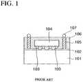
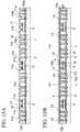
- the wafer level CSPhas a structure shown in FIG. 1 , for example.
- wirings 102are formed on a first semiconductor device chip 101 , and a second semiconductor device chip 104 is secured to the wirings 102 via solder balls 103 .
- the second semiconductor device chip 104is smaller in size than the first semiconductor device chip 101 .
- pin type terminals (vias) 105are connected to the wirings 102 on the first semiconductor device chip 101 in the peripheral area of the second semiconductor device chip 104 .
- a sealing resin 106 for sealing the second semiconductor device chip 104is formed on an upper surface of the first semiconductor device chip 101 to have such a thickness that upper ends of the terminals 105 are exposed from the resin.
- a solder ball 107is connected to the upper ends of the terminals 105 respectively.
- the terminals 105 shown in FIG. 1are formed on the wirings 102 by the plating method. Thus, it takes much time to form the terminals 105 and thus throughput of the CSP formation is gone down.
- forming areas of the terminals 105are limited to the periphery of the second semiconductor device chip 104 . Thus, it is not expected to increase the number of the terminals 105 .
- a semiconductor devicewhich comprises a first semiconductor chip having a first terminal on one surface; a second semiconductor chip which is larger than the first semiconductor chip and on which the first semiconductor chip is stacked, and which has a second terminal on one surface; an insulating layer formed on second semiconductor chip to cover the first semiconductor chip; a plurality of holes formed in the insulating layer; a conductive via formed like a film on inner peripheral surfaces and bottom surfaces of the holes and connected electrically to at least one of the first terminal and the second terminal; a first wiring pattern formed on an upper surface of the insulating layer; and an external terminal formed on the first wiring pattern.
- the insulating layer for covering the first semiconductor chipis formed on the second semiconductor chip, the holes are formed in the insulating layer, the film-like vias are formed in the hole respectively, and the wiring patterns are formed on the insulating layer.
- the viascan be formed in a short time, and both the wiring patterns and the vias can be formed by the same conductive film, and thus the number of the film forming steps can be reduced.
- the wiring patterns formed on the insulating layerare led onto the first semiconductor chip and then the external terminals are formed on the wiring patterns. Therefore, the narrower pitch between plural external terminals on the insulating layer can be suppressed, and also the number of the external terminals can be increased.
- corrosion of the viascan be prevented by covering the vias in the holes with the insulating layer.
- migration short and corrosion of the first wiring patternscan be prevented by covering the first wiring patterns except the portions to be connected to the wiring patterns on the insulating layer with another insulating layer.
- the wafer-level laminated packagecan be formed by the same technology independently of whether a circuit surface of the first semiconductor chip on which the first terminals are formed is face-up or face-down bonded on a circuit surface of the second semiconductor chip on which the first terminals are formed. Also, the face up bonding or the face down bonding can be used in its proper way, and also the semiconductor devices having various functions can be stacked. Therefore, the present invention is useful.
- the external terminalscan be formed at any positions to correspond to a multi-pin structure.
- a plurality of semiconductor chipscan be mounted by forming the above insulating layer having the wiring patterns and the vias therein as a multi-layered structure or by stacking the above mentioned structures.
- FIG. 1is a sectional view showing a semiconductor device having the conventional structure
- FIGS. 2A to 2Care sectional views (# 1 ) showing steps of manufacturing a semiconductor device according to a first embodiment of the present invention
- FIGS. 3A to 3Care sectional views (# 2 ) showing steps of manufacturing the semiconductor device according to the first embodiment of the present invention
- FIGS. 4A and 4Bare sectional views (# 3 ) showing steps of manufacturing the semiconductor device according to the first embodiment of the present invention
- FIGS. 5A and 5Bare sectional views (# 4 ) showing steps of manufacturing the semiconductor device according to the first embodiment of the present invention
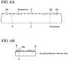
- FIG. 6Ais a sectional view showing a semiconductor wafer constituting the semiconductor device according to the first embodiment of the present invention.
- FIG. 6Bis a sectional view showing a semiconductor device chip constituting the semiconductor device according to the first embodiment of the present invention.
- FIG. 7is a sectional view showing the semiconductor device according to the first embodiment of the present invention.
- FIG. 8is a sectional view showing a semiconductor device having a multi-layered wiring structure according to the first embodiment of the present invention.
- FIGS. 9A and 9Bare sectional views showing steps of manufacturing a semiconductor device according to a second embodiment of the present invention.
- FIG. 10is a sectional view showing the semiconductor device according to the second embodiment of the present invention.
- FIGS. 11A to 11Care sectional views (# 1 ) showing steps of manufacturing a semiconductor device according to a third embodiment of the present invention.
- FIGS. 12A and 12Bare sectional views (# 2 ) showing steps of manufacturing the semiconductor device according to the third embodiment of the present invention.
- FIGS. 13A and 13Bare sectional views (# 3 ) showing steps of manufacturing the semiconductor device according to the third embodiment of the present invention.
- FIG. 14is a sectional view showing the semiconductor device according to the third embodiment of the present invention.
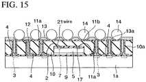
- FIG. 15is a sectional view showing a first semiconductor device according to a fourth embodiment of the present invention.
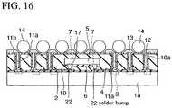
- FIG. 16is a sectional view showing a second semiconductor device according to the fourth embodiment of the present invention.
- FIG. 2 to FIG. 5are sectional views showing steps of forming a multi-chip package (MCP) according to a first embodiment of the present invention.
- MCPmulti-chip package
- a semiconductor wafer 1 in which a first semiconductor circuit (not shown) is formed in a plurality of device areas A respectivelyis prepared.
- the semiconductor wafer 1has a protection insulating layer 2 on its upper surface, as shown in a fragmental enlarged view of FIG. 6A , and openings 2 a to expose a first terminal (conductive pad) 3 that is connected electrically to an internal wiring (not shown) of the semiconductor device are formed in the protection insulating layer 2 .
- the first terminal 3is formed of aluminum, copper, or the like.
- the semiconductor wafer 1is composed of a silicon wafer, for example, and is cut away in the later step every first semiconductor circuit and divided into the device area A unit.
- first rewiring patterns 4are formed by forming a metal film having a double-layered structure made of titanium and nickel on the protection insulating layer 2 and the first terminals 3 to have a thickness of about 0.5 f ⁇ m, and then patterning the metal film by means of the photolithography method.
- the first rewiring pattern 4is a conductive pattern that is led from an upper surface of the first terminal 3 to an upper surface of the protection insulating layer 2 .
- first semiconductor device chips 5 on which a second semiconductor circuit (not shown) is formed respectivelyare prepared.
- the first semiconductor device chip 5is formed of a silicon chip, for example, which is smaller than the device area A of the semiconductor wafer 1 , and has a protection insulating layer 6 on its upper surface. Openings 6 a to expose second terminals 7 that are connected to wirings (not shown) in the first semiconductor device chip 5 are formed in the protection insulating layer 6 . Also, second rewiring patterns 8 each of which is led from an upper surface of the second terminal 7 are formed on the protection insulating layer 6 .
- each first semiconductor device chip 5is bonded to a center portion of the device area A of the semiconductor wafer 1 via a die bonding agent (adhesive) 9 .
- a resin insulating layer 10 made of epoxy, polyimide, or the likeis formed on an upper surface of the semiconductor wafer 1 to have a thickness that is higher than the first semiconductor device chip 5 by about 10 to 20 f ⁇ m.
- the first semiconductor device chips 5are covered with the resin insulating layer 10 .
- the resin insulating layer 10is formed on the semiconductor wafer 1 by the spin coating, the printing, the laminating method, or the like.
- a countermeasure to prevent generation of the bubble in overlying areas of the first semiconductor device chips 5 and their peripheral areasmust be taken by adjusting sufficiently a film thickness of the resin insulating layer 10 , etc.
- the resin insulating layer 10made of epoxy resin, polyimide, or the like, for example, is formed on the semiconductor wafer 1 to have a thickness of 120 to 150 f ⁇ m, for example, and then the upper surface of the resin insulating layer 10 is planarized by the mechanical polishing method or the chemical-mechanical polishing method.
- via holes (through holes) 10 aeach having a diameter of 80 to 100 f ⁇ m are formed in the resin insulating layer 10 on the first rewiring patterns 4 and the second rewiring patterns 8 respectively.
- the via holes 10 aare formed easily by exposing the resin insulating layer 10 by using an exposure mask for the via hole formation and then developing the resin insulating layer 10 by using an inorganic alkaline solution such as sodium carbonate (NaCO 3 ), or the like after the resin insulating layer 10 is formed on the semiconductor wafer 1 in the non-exposure light environment.
- an inorganic alkaline solutionsuch as sodium carbonate (NaCO 3 ), or the like after the resin insulating layer 10 is formed on the semiconductor wafer 1 in the non-exposure light environment.
- the via holes 10 ashould be formed by irradiating a high energy such as the laser, or the like onto predetermined positions of the resin insulating layer 10 .
- a high energysuch as the laser, or the like
- the via holes 10 aare formed by the laser, it is not possible that the first terminals 3 made of the relatively soft conductive material such as aluminum, copper, or the like and the neighboring protection insulating layer 2 are removed or deteriorated by the laser irradiation because the first terminals 3 and the protection insulating layer 2 located under the via holes 10 a are covered with the first rewiring pattern 4 made of a hard metal.
- the via holes 10 amay be formed by the drilling.
- the surface of the resin insulating layer 10is activated by the diluent solvent, and then a metal film 11 , e.g., a copper film, of 0.5 to 1.0 f ⁇ m thickness is formed on the upper surface of the resin insulating layer 10 and inner peripheral surfaces and bottom surfaces of the via holes 10 a by the electroless plating.
- the metal film 11 having such thicknessis formed in a very short time in contrast to the case where the external terminals 105 shown in FIG. 1 are formed by the plating. In this case, the metal film 11 is connected to the upper surfaces of the first rewiring patterns 4 in the via holes 10 a .
- the metal filmmay be formed herein to have a multi-layered structure.
- the metal film 11when it is desired to form the metal film 11 of about 3 to 5 f ⁇ m thickness, a method for forming the film thin once by virtue of the electroless plating method and then forming the film thick by virtue of the electroplating method may be employed. Also, in the case where the resin insulating layer 10 is formed of epoxy resin or polyimide, the growth of the metal film 11 on the upper surface of the resin insulating layer 10 and the inner surfaces of the via holes 10 a by the electroless plating is easy.
- the metal film 11is patterned by the photolithography method.
- the metal film 11 in the via holes 10 ais left as vias 11 a and also patterns of the metal film 11 on the upper surface of the resin insulating layer 10 are used as third rewiring patterns 11 b .
- a plurality of third rewiring patterns 11 b on the resin insulating layer 10are connected electrically to the second terminals 7 of the first semiconductor device chips 5 via the holes 10 a and the second rewiring patterns 8 respectively, and also connected electrically to the first terminals 3 of the semiconductor wafer 1 via the vias 11 a and the first rewiring patterns 4 .
- the second terminals 7 of the first semiconductor device chips 5are connected electrically to the first terminals 3 of the semiconductor wafer 1 via the vias 11 a and the third rewiring patterns 11 b respectively.
- all the vias 11 aare connected to the third rewiring patterns 11 b respectively, but the vias 11 a that are not connected to such pattern may be provided.
- buried insulating layers 12are formed by filling the non-photosensitive epoxy resin into the opening portions 10 a in the resin insulating layer 10 by using the squeegee or the printing method.
- the via 11 a in the opening portion 10 ais covered with the buried insulating layer 12 .
- an insulating resin cover layer 13 made of a photosensitive epoxy resin, a photosensitive novolak resin, or the likeis formed on the resin insulating layer 10 , the third rewiring patterns 11 b , and the buried insulating layers 12 respectively.
- the resin cover layer 13is coated on the resin insulating layer 10 in the non-exposure light environment by using the squeegee or by the printing method.
- the resin cover layer 13prevents corrosion of the third rewiring patterns 11 b and prevents the migration short of the third rewiring patterns 11 b.
- openings 13 a for exposing contact portions of the third rewiring patterns 11 bare patterned by exposing/developing the resin cover layer 13 .
- the semiconductor deviceis divided into a plurality of second semiconductor device chips 1 a by dicing boundaries between the device areas A of the semiconductor wafer 1 shown in FIG. 5B .
- a plurality of MCP semiconductor devices shown in FIG. 7are formed.
- side surfaces of the second semiconductor device chip 1 aare not covered with the resin insulating layer 10 to expose.
- a bottom surface of the semiconductor wafer 1may be polished by the mechanical polishing method or the chemical-mechanical polishing method.
- the via holes 10 aare formed around the first semiconductor device chips 5 in the resin insulating layer 10 formed on the upper surfaces of the second semiconductor device chips 1 a , also the conductive films formed on the inner peripheral surfaces and the bottom surfaces of the via holes 10 a are used as the vias 11 a , and also the conductive films on the upper surface of the resin insulating layer 10 are used as the third rewiring patterns 11 b.
- the formation of the vias 11 a to be formed in the via holes 10 ais executed by the step of forming the metal film 11 .
- the viascan be formed in a short time rather than the conventional structure in which the via holes are buried completely.
- the portion of the metal film 11 constituting the via 11 awhich is formed on the upper surface of the resin insulating layer 10 , is patterned and used as the third rewiring pattern 11 b .
- the external terminals 14are formed over the first semiconductor device chips 5 , so that the number of the external terminals 14 can be increased rather than the prior art and also a narrower pitch between the external terminals 14 can be relaxed.
- both the vias 11 a and the third rewiring patterns 11 bare formed by the same metal film 11 , the throughput can be improved rather than the case they are formed separately respectively.
- the first semiconductor device chips 5are adhered onto the semiconductor wafer 1 , then the resin insulating layer 10 , the vias 11 a , the third rewiring patterns 11 b , the resin cover layer 13 , and the external terminals 14 are formed, and then the semiconductor wafer 1 is divided separately.
- first the semiconductor wafer 1may be divided into a plurality of second semiconductor device chips 1 a , then the first semiconductor device chips 5 may be adhered onto the second semiconductor device chips 1 a respectively, and then the resin insulating layer 10 , the vias 11 a , the third rewiring patterns 11 b , the resin cover layer 13 , and the external terminals 14 may be formed.
- the semiconductor device having the same structure as shown in FIG. 7is also formed. In this case, the side surfaces of the second semiconductor device chip 1 a are covered with the resin insulating layer 10 .
- the wiring structure layers having the resin insulating layer 10 , the vias 11 a , and the third rewiring patterns 11 bmay be formed as a multi-layered wiring structure having two layers or more.
- the resin cover layer 13 and the external terminals 14are formed on the uppermost resin insulating layer 10 .
- upper and lower rewiring patterns 11 bare arranged in such a manner that they intersect with each other to deal with the high-speed signal processing.
- Such multi-layered wiring structuremay be employed in embodiments given in the following.
- the vias 11 a and the third rewiring patterns 11 bare formed, then the buried insulating layers 12 are formed in the via holes 10 a , and then the resin cover layer 13 is formed on the resin insulating layer 10 .
- the buried insulating layers 12 and the resin cover layer 13may be formed at the same time.
- a photosensitive resin layer 15e.g., an epoxy resin
- a photosensitive resin layer 15is coated simultaneously in the via holes 10 a and on the resin insulating layer 10 , and then openings 15 a to expose the contact portions of the third rewiring patterns 11 b are formed by exposing/developing the resin layer 15 .
- the epoxy resin in the via holes 10 ais used as the buried insulating layers respectively, and the epoxy resin on the resin insulating layer 10 is used as the resin cover layer. Also, the buried insulating layers and the resin cover layer can be formed at the same time, whereby the number of the steps of forming the insulating layer can be reduced in contrast to the first embodiment.
- a semiconductor device shown in FIG. 10is formed by cutting off the boundaries between the device areas A.
- the side surfaces of the second semiconductor device chip 1 aare not covered with the resin insulating layer 10 and are exposed.
- a coating conductive layer 16 made of nickel-phosphorus (NiP), nickel, gold, or the likeis formed selectively on the first terminals 3 in the openings 2 a of the protection insulating layer 2 on the semiconductor wafer 1 by the electroless plating method to have a thickness of 3 to 5 f ⁇ m.
- the first semiconductor device chips 5are secured onto the semiconductor wafer 1 by the same method as the first embodiment.
- a chip having a structure in which not the second rewiring pattern but a coating conductive layer 17 made of NiP is formed on the second terminals 7 in the protection insulating layer 6 on the upper surfaceis employed.
- the resin insulating layer 10is formed on the semiconductor wafer 1 to cover the first semiconductor device chip 5 .
- the same methods as the first embodimentare employed to form and planarize the resin insulating layer 10 .
- the via holes 10 aare formed in the resin insulating layer 10 on the coating conductive layers 16 , 17 on the first and second terminals 3 , 7 on the semiconductor wafer 1 and the first semiconductor device chip 5 respectively.
- the via holes 10 aare formed by the exposure and the development when the resin insulating layer 10 is formed of the photosensitive material, while the via holes 10 a are formed by the laser irradiation when the resin insulating layer 10 is formed of the non-photosensitive material.
- the via holes 10 amay be formed by the drilling.
- the vias 11 a and the third rewiring patterns 11 bare formed in the via holes 10 a and on the resin insulating layer 10 via the steps similar to those in the first embodiment respectively.
- the buried insulating layers 12 , the cover insulating layer 13 , and the external terminals 14are formed.
- the buried insulating layers 12 and the cover insulating layer 13may be formed of the same resin layer 15 at the same time, as shown in the second embodiment.
- the semiconductor wafer 1is divided into a plurality of second semiconductor device chips 1 a every device area A.
- a semiconductor device shown in FIG. 14is formed.
- the side surfaces of the second semiconductor device chip 1 aare not covered with the resin insulating layer 10 and exposed.
- the inorganic alkali used to form the via holes 10 a in the resin insulating layer 10can be prevented from being supplied to the terminals 3 , 7 by the coating conductive layers 16 , 17 , or the laser used to form the via holes 10 a can be prevented from being irradiated onto the terminals 3 , 7 by the coating conductive layers 16 , 17 .
- the degradation of the first and second terminals 3 , 7can be prevented.
- the rewiring patternsmay be formed on any one of the first semiconductor device chips 5 and the semiconductor wafer 1 .
- the terminals 3 , 7 that are not covered with the rewiring patternsmust be covered with the coating conductive layers 16 , 17 .
- the first semiconductor device chips 5 shown in FIG. 6Bmay be connected to the first terminals 3 on the semiconductor wafer 1 via not the third rewiring patterns 11 b formed on the upper surface of the resin insulating layer 10 but the wires or the solder balls.
- such a structuremay be employed that not the rewiring patterns but the coating conductive layers 17 made of nickel-phosphorus are formed on the second terminal 7 of the first semiconductor device chip 5 and then the coating conductive layers 17 and the first rewiring patterns 4 on the semiconductor wafer 1 (the second semiconductor device chip 1 a ) are connected via gold (conductive) wires 21 by the wire bonding.
- no via hole 10 ais formed in the resin insulating layer 10 on the first semiconductor device chip 5 .
- solder bumps (external terminals) 22may be connected onto the second terminal 7 of the first semiconductor device chip 5 , and then the solder bumps 22 may be connected onto the first rewiring patterns 4 on the semiconductor wafer 1 (the second semiconductor device chip 1 a ). In this case, no via hole 10 a is also formed in the resin insulating layer 10 on the first semiconductor device chip 5 .
- the via holes 10 aare not formed in the resin insulating layer 10 shown in FIG. 15 , FIG. 16 over the first semiconductor device chips 5 , but the third rewiring patterns 11 b are formed on the resin insulating layer 10 and then the external terminals 14 are bonded thereon.
- the forming areas of the external terminals 14 on the resin insulating layer 10can be widened rather than the prior art, and the number of the external terminals 14 can be increased rather than the prior art, and also the narrower pitch between the external terminals 14 can be relaxed.
- the insulating layer for covering the first semiconductor chipis formed on the second semiconductor chip, the holes are formed in the insulating layer, the film-like vias are formed in the hole respectively, and the wiring patterns are formed on the insulating layer. Therefore, the vias can be formed in a short time, and both the wiring patterns and the vias can be formed by the same conductive film, and thus the number of the film forming steps can be reduced.
- the wiring patterns on the insulating layerare led onto the first semiconductor chip and then the external terminals are formed on the wiring patterns. Therefore, the narrower pitch between plural external terminals on the insulating layer can be suppressed, and also the number of the external terminals can be increased.
- corrosion of the viascan be prevented by covering the vias in the holes with the insulating layer, and also migration short and corrosion of the first wiring patterns can be prevented by covering the first wiring patterns on the insulating layer except the portions to be connected to the external terminals with another insulating layer.
Landscapes
- Engineering & Computer Science (AREA)
- Microelectronics & Electronic Packaging (AREA)
- Power Engineering (AREA)
- Computer Hardware Design (AREA)
- Physics & Mathematics (AREA)
- Condensed Matter Physics & Semiconductors (AREA)
- General Physics & Mathematics (AREA)
- Manufacturing & Machinery (AREA)
- Internal Circuitry In Semiconductor Integrated Circuit Devices (AREA)
Abstract
Description
Claims (8)
Priority Applications (1)
| Application Number | Priority Date | Filing Date | Title |
|---|---|---|---|
| US11/477,550US7759246B2 (en) | 2001-12-07 | 2006-06-30 | Semiconductor device having a plurality of semiconductor chips and method for manufacturing the same |
Applications Claiming Priority (3)
| Application Number | Priority Date | Filing Date | Title |
|---|---|---|---|
| PCT/JP2001/010722WO2003049184A1 (en) | 2001-12-07 | 2001-12-07 | Semiconductor device and method for manufacturing the same |
| US10/860,657US7084513B2 (en) | 2001-12-07 | 2004-06-04 | Semiconductor device having a plurality of semiconductor chips and method for manufacturing the same |
| US11/477,550US7759246B2 (en) | 2001-12-07 | 2006-06-30 | Semiconductor device having a plurality of semiconductor chips and method for manufacturing the same |
Related Parent Applications (1)
| Application Number | Title | Priority Date | Filing Date |
|---|---|---|---|
| US10/860,657DivisionUS7084513B2 (en) | 2001-12-07 | 2004-06-04 | Semiconductor device having a plurality of semiconductor chips and method for manufacturing the same |
Publications (2)
| Publication Number | Publication Date |
|---|---|
| US20060246623A1 US20060246623A1 (en) | 2006-11-02 |
| US7759246B2true US7759246B2 (en) | 2010-07-20 |
Family
ID=11738006
Family Applications (2)
| Application Number | Title | Priority Date | Filing Date |
|---|---|---|---|
| US10/860,657Expired - Fee RelatedUS7084513B2 (en) | 2001-12-07 | 2004-06-04 | Semiconductor device having a plurality of semiconductor chips and method for manufacturing the same |
| US11/477,550Expired - Fee RelatedUS7759246B2 (en) | 2001-12-07 | 2006-06-30 | Semiconductor device having a plurality of semiconductor chips and method for manufacturing the same |
Family Applications Before (1)
| Application Number | Title | Priority Date | Filing Date |
|---|---|---|---|
| US10/860,657Expired - Fee RelatedUS7084513B2 (en) | 2001-12-07 | 2004-06-04 | Semiconductor device having a plurality of semiconductor chips and method for manufacturing the same |
Country Status (6)
| Country | Link |
|---|---|
| US (2) | US7084513B2 (en) |
| EP (1) | EP1455392A4 (en) |
| JP (1) | JP4182189B2 (en) |
| KR (1) | KR100636259B1 (en) |
| CN (1) | CN100350607C (en) |
| WO (1) | WO2003049184A1 (en) |
Cited By (6)
| Publication number | Priority date | Publication date | Assignee | Title |
|---|---|---|---|---|
| US20080029890A1 (en)* | 2006-08-03 | 2008-02-07 | Unimicron Technology Corp. | Embedded chip package process and circuit board with embedded chip |
| US20120038053A1 (en)* | 2010-08-16 | 2012-02-16 | Stats Chippac, Ltd. | Semiconductor Device and Method of Forming FO-WLCSP Having Conductive Layers and Conductive Vias Separated by Polymer Layers |
| US9330994B2 (en) | 2014-03-28 | 2016-05-03 | Stats Chippac, Ltd. | Semiconductor device and method of forming RDL and vertical interconnect by laser direct structuring |
| US9397057B2 (en)* | 2014-06-02 | 2016-07-19 | Kabushiki Kaisha Toshiba | Plurality of semiconductor devices in resin with a via |
| US9653372B2 (en) | 2014-10-23 | 2017-05-16 | Samsung Electronics Co., Ltd. | Method for fabricating fan-out wafer level package and fan-out wafer level package fabricated thereby |
| US11264538B2 (en) | 2016-03-10 | 2022-03-01 | Soft-Epi Inc. | Near-ultraviolet light-emitting semiconductor light-emitting element and group III nitride semiconductor template used therefor |
Families Citing this family (74)
| Publication number | Priority date | Publication date | Assignee | Title |
|---|---|---|---|---|
| US6710454B1 (en) | 2000-02-16 | 2004-03-23 | Micron Technology, Inc. | Adhesive layer for an electronic apparatus having multiple semiconductor devices |
| WO2003049184A1 (en)* | 2001-12-07 | 2003-06-12 | Fujitsu Limited | Semiconductor device and method for manufacturing the same |
| US9691635B1 (en) | 2002-05-01 | 2017-06-27 | Amkor Technology, Inc. | Buildup dielectric layer having metallization pattern semiconductor package fabrication method |
| US7633765B1 (en)* | 2004-03-23 | 2009-12-15 | Amkor Technology, Inc. | Semiconductor package including a top-surface metal layer for implementing circuit features |
| US7548430B1 (en) | 2002-05-01 | 2009-06-16 | Amkor Technology, Inc. | Buildup dielectric and metallization process and semiconductor package |
| KR100574947B1 (en)* | 2003-08-20 | 2006-05-02 | 삼성전자주식회사 | BA package, manufacturing method thereof and BA package laminated structure |
| JP4271590B2 (en)* | 2004-01-20 | 2009-06-03 | 新光電気工業株式会社 | Semiconductor device and manufacturing method thereof |
| US11081370B2 (en) | 2004-03-23 | 2021-08-03 | Amkor Technology Singapore Holding Pte. Ltd. | Methods of manufacturing an encapsulated semiconductor device |
| US10811277B2 (en) | 2004-03-23 | 2020-10-20 | Amkor Technology, Inc. | Encapsulated semiconductor package |
| TWI250596B (en) | 2004-07-23 | 2006-03-01 | Ind Tech Res Inst | Wafer-level chip scale packaging method |
| DE102004048203A1 (en)* | 2004-09-30 | 2005-12-29 | Infineon Technologies Ag | Stackable semiconductor module for electronics packaging has electronic component with vertical opening provided with continuous metallization with layer of soldering paste to connect it to contact of another electronic component |
| KR101198038B1 (en)* | 2005-01-28 | 2012-11-06 | 듀크 유니버서티 | Apparatuses and methods for manipulating droplets on a printed circuit board |
| US20060237828A1 (en)* | 2005-04-22 | 2006-10-26 | Robinson William D | System and method for enhancing wafer chip scale packages |
| US9601474B2 (en) | 2005-07-22 | 2017-03-21 | Invensas Corporation | Electrically stackable semiconductor wafer and chip packages |
| JP4395775B2 (en)* | 2005-10-05 | 2010-01-13 | ソニー株式会社 | Semiconductor device and manufacturing method thereof |
| TWI284976B (en)* | 2005-11-14 | 2007-08-01 | Via Tech Inc | Package, package module and manufacturing method of the package |
| JP2007207921A (en)* | 2006-01-31 | 2007-08-16 | Stanley Electric Co Ltd | Manufacturing method of surface mount type optical semiconductor device |
| US7884464B2 (en)* | 2006-06-27 | 2011-02-08 | Advanced Chip Engineering Technologies Inc. | 3D electronic packaging structure having a conductive support substrate |
| WO2008014633A1 (en)* | 2006-06-29 | 2008-02-07 | Intel Corporation | Apparatus, system, and method for wireless connection in integrated circuit packages |
| KR100800476B1 (en)* | 2006-07-11 | 2008-02-04 | 삼성전자주식회사 | Semiconductor package and manufacturing method thereof and semiconductor module and manufacturing method thereof |
| TWI335658B (en)* | 2006-08-22 | 2011-01-01 | Advanced Semiconductor Eng | Stacked structure of chips and wafer structure for making same |
| DE102007030986A1 (en)* | 2006-10-25 | 2008-04-30 | Robert Bosch Gmbh | Electrical component i.e. micromechanical sensor, has contact units provided as solder beads and/or copper supports and arranged at side of one of chips, and cover partially surrounding chip at side and/or partially surrounding other chip |
| US7550857B1 (en) | 2006-11-16 | 2009-06-23 | Amkor Technology, Inc. | Stacked redistribution layer (RDL) die assembly package |
| US8178982B2 (en)* | 2006-12-30 | 2012-05-15 | Stats Chippac Ltd. | Dual molded multi-chip package system |
| US8304923B2 (en)* | 2007-03-29 | 2012-11-06 | ADL Engineering Inc. | Chip packaging structure |
| KR100871380B1 (en)* | 2007-06-18 | 2008-12-02 | 주식회사 하이닉스반도체 | Semiconductor Package with Passive Device |
| JP5215605B2 (en)* | 2007-07-17 | 2013-06-19 | ラピスセミコンダクタ株式会社 | Manufacturing method of semiconductor device |
| US8293587B2 (en)* | 2007-10-11 | 2012-10-23 | International Business Machines Corporation | Multilayer pillar for reduced stress interconnect and method of making same |
| KR20090055316A (en)* | 2007-11-28 | 2009-06-02 | 삼성전자주식회사 | Semiconductor package, method for manufacturing electronic device and semiconductor package having same |
| US8847377B2 (en) | 2008-01-02 | 2014-09-30 | SK Hynix Inc. | Stacked wafer level package having a reduced size |
| KR100910233B1 (en)* | 2008-01-02 | 2009-07-31 | 주식회사 하이닉스반도체 | Stacked Wafer Level Packages |
| EP2246979A4 (en) | 2008-02-18 | 2014-03-05 | Murata Manufacturing Co | Elastic wave device and method for manufacturing the same |
| US8637341B2 (en)* | 2008-03-12 | 2014-01-28 | Infineon Technologies Ag | Semiconductor module |
| US8362617B2 (en)* | 2008-05-01 | 2013-01-29 | Infineon Technologies Ag | Semiconductor device |
| US7888184B2 (en)* | 2008-06-20 | 2011-02-15 | Stats Chippac Ltd. | Integrated circuit packaging system with embedded circuitry and post, and method of manufacture thereof |
| US8354304B2 (en)* | 2008-12-05 | 2013-01-15 | Stats Chippac, Ltd. | Semiconductor device and method of forming conductive posts embedded in photosensitive encapsulant |
| US20100148337A1 (en)* | 2008-12-17 | 2010-06-17 | Yong Liu | Stackable semiconductor package and process to manufacture same |
| US8003445B2 (en)* | 2009-03-26 | 2011-08-23 | Stats Chippac Ltd. | Integrated circuit packaging system with z-interconnects having traces and method of manufacture thereof |
| JP5165006B2 (en)* | 2010-01-25 | 2013-03-21 | 株式会社テラミクロス | Manufacturing method of semiconductor device |
| US8138014B2 (en)* | 2010-01-29 | 2012-03-20 | Stats Chippac, Ltd. | Method of forming thin profile WLCSP with vertical interconnect over package footprint |
| US8455300B2 (en) | 2010-05-25 | 2013-06-04 | Stats Chippac Ltd. | Integrated circuit package system with embedded die superstructure and method of manufacture thereof |
| JP5703010B2 (en) | 2010-12-16 | 2015-04-15 | 新光電気工業株式会社 | Semiconductor package and manufacturing method thereof |
| US8765525B2 (en) | 2011-06-16 | 2014-07-01 | Stats Chippac Ltd. | Method of manufacturing an integrated circuit packaging system including lasering through encapsulant over interposer |
| TWI469292B (en)* | 2011-07-26 | 2015-01-11 | 萬國半導體股份有限公司 | Stacked power semiconductor device using dual lead frame and manufacturing method |
| US8487421B2 (en)* | 2011-08-01 | 2013-07-16 | Tessera, Inc. | Microelectronic package with stacked microelectronic elements and method for manufacture thereof |
| US20130040423A1 (en)* | 2011-08-10 | 2013-02-14 | Taiwan Semiconductor Manufacturing Company, Ltd. | Method of Multi-Chip Wafer Level Packaging |
| CN103383927A (en)* | 2012-05-03 | 2013-11-06 | 三星电子株式会社 | Semiconductor encapsulation and forming method thereof |
| US8901730B2 (en) | 2012-05-03 | 2014-12-02 | Taiwan Semiconductor Manufacturing Company, Ltd. | Methods and apparatus for package on package devices |
| TWI562295B (en) | 2012-07-31 | 2016-12-11 | Mediatek Inc | Semiconductor package and method for fabricating base for semiconductor package |
| US9177899B2 (en)* | 2012-07-31 | 2015-11-03 | Mediatek Inc. | Semiconductor package and method for fabricating base for semiconductor package |
| US10991669B2 (en) | 2012-07-31 | 2021-04-27 | Mediatek Inc. | Semiconductor package using flip-chip technology |
| US8778738B1 (en) | 2013-02-19 | 2014-07-15 | Taiwan Semiconductor Manufacturing Company, Ltd. | Packaged semiconductor devices and packaging devices and methods |
| US9953907B2 (en)* | 2013-01-29 | 2018-04-24 | Taiwan Semiconductor Manufacturing Company, Ltd. | PoP device |
| US8970023B2 (en) | 2013-02-04 | 2015-03-03 | Taiwan Semiconductor Manufacturing Company, Ltd. | Package structure and methods of forming same |
| KR101488590B1 (en) | 2013-03-29 | 2015-01-30 | 앰코 테크놀로지 코리아 주식회사 | Semiconductor device and manufacturing method thereof |
| US9446943B2 (en) | 2013-05-31 | 2016-09-20 | Stmicroelectronics S.R.L. | Wafer-level packaging of integrated devices, and manufacturing method thereof |
| US9653442B2 (en)* | 2014-01-17 | 2017-05-16 | Taiwan Semiconductor Manufacturing Company, Ltd. | Integrated circuit package and methods of forming same |
| US9704841B2 (en) | 2014-03-26 | 2017-07-11 | United Microelectronics Corp. | Method of packaging stacked dies on wafer using flip-chip bonding |
| KR102161776B1 (en)* | 2014-03-28 | 2020-10-06 | 에스케이하이닉스 주식회사 | Stack package |
| US11239138B2 (en)* | 2014-06-27 | 2022-02-01 | Taiwan Semiconductor Manufacturing Company | Methods of packaging semiconductor devices and packaged semiconductor devices |
| US10177115B2 (en) | 2014-09-05 | 2019-01-08 | Taiwan Semiconductor Manufacturing Company, Ltd. | Package structures and methods of forming |
| US9802813B2 (en) | 2014-12-24 | 2017-10-31 | Stmicroelectronics (Malta) Ltd | Wafer level package for a MEMS sensor device and corresponding manufacturing process |
| US9627311B2 (en) | 2015-01-22 | 2017-04-18 | Mediatek Inc. | Chip package, package substrate and manufacturing method thereof |
| KR102505189B1 (en)* | 2015-07-22 | 2023-03-02 | 인텔 코포레이션 | multi-layer package |
| US20170098629A1 (en) | 2015-10-05 | 2017-04-06 | Mediatek Inc. | Stacked fan-out package structure |
| US11037904B2 (en) | 2015-11-24 | 2021-06-15 | Taiwan Semiconductor Manufacturing Company, Ltd. | Singulation and bonding methods and structures formed thereby |
| US10068853B2 (en)* | 2016-05-05 | 2018-09-04 | Taiwan Semiconductor Manufacturing Co., Ltd. | Integrated fan-out package and method of fabricating the same |
| US10177078B2 (en)* | 2016-11-28 | 2019-01-08 | Taiwan Semiconductor Manufacturing Co., Ltd. | Method for forming chip package structure |
| US10510722B2 (en)* | 2017-06-20 | 2019-12-17 | Taiwan Semiconductor Manufacturing Company Ltd. | Semiconductor device and method for manufacturing the same |
| US10879220B2 (en)* | 2018-06-15 | 2020-12-29 | Taiwan Semiconductor Manufacturing Company, Ltd. | Package-on-package structure and manufacturing method thereof |
| CN110875294B (en)* | 2018-08-29 | 2024-01-23 | 恒劲科技股份有限公司 | Package structure of semiconductor device and method for manufacturing the same |
| CN111341750B (en)* | 2018-12-19 | 2024-03-01 | 奥特斯奥地利科技与系统技术有限公司 | Component carrier comprising an electrically conductive base structure and method of manufacture |
| US11063019B2 (en)* | 2019-07-17 | 2021-07-13 | Taiwan Semiconductor Manufacturing Company, Ltd. | Package structure, chip structure and method of fabricating the same |
| US11735554B2 (en)* | 2020-08-14 | 2023-08-22 | Sj Semiconductor (Jiangyin) Corporation | Wafer-level chip scale packaging structure having a rewiring layer and method for manufacturing the wafer-level chip scale packaging structure |
Citations (24)
| Publication number | Priority date | Publication date | Assignee | Title |
|---|---|---|---|---|
| US5430329A (en)* | 1991-01-29 | 1995-07-04 | Mitsubishi Denki Kabushiki Kaisha | Semiconductor device with bonding pad electrode |
| EP0706208A2 (en) | 1994-10-03 | 1996-04-10 | Kabushiki Kaisha Toshiba | Semiconductor package integral with semiconductor chip and method of manufacturing thereof |
| US5903049A (en) | 1997-10-29 | 1999-05-11 | Mitsubishi Denki Kabushiki Kaisha | Semiconductor module comprising semiconductor packages |
| US6100594A (en) | 1998-01-14 | 2000-08-08 | Sharp Kabushiki Kaisha | Semiconductor device and method of manufacturing the same |
| US6181002B1 (en) | 1998-12-22 | 2001-01-30 | Sharp Kabushiki Kaisha | Semiconductor device having a plurality of semiconductor chips |
| KR20010063892A (en) | 1999-12-24 | 2001-07-09 | 박종섭 | Wafer level multi-chip package and the manufacturing method |
| JP2001217381A (en) | 2000-01-28 | 2001-08-10 | Fujitsu Ltd | Semiconductor device and method of manufacturing semiconductor device |
| US20010015496A1 (en) | 2000-02-21 | 2001-08-23 | Kazumi Watase | Semiconductor device and method for the fabrication thereof |
| JP2001250836A (en) | 2000-03-06 | 2001-09-14 | Casio Comput Co Ltd | Semiconductor device and method of manufacturing the same |
| JP2001257310A (en) | 2000-03-09 | 2001-09-21 | Oki Electric Ind Co Ltd | Semiconductor device and method of manufacturing therefor, and testing method for the same |
| JP2001298149A (en) | 2000-04-14 | 2001-10-26 | Matsushita Electric Ind Co Ltd | Semiconductor device and method of manufacturing the same |
| US6344682B1 (en) | 1999-02-01 | 2002-02-05 | Mitsubishi Denki Kabushiki Kaisha | Semiconductor device comprising a semiconductor element mounted on a substrate and covered by a wiring board |
| JP2002050721A (en) | 2000-08-03 | 2002-02-15 | Hitachi Cable Ltd | Electronic device and method of manufacturing the same |
| US6452278B1 (en) | 2000-06-30 | 2002-09-17 | Amkor Technology, Inc. | Low profile package for plural semiconductor dies |
| US6476500B2 (en) | 2000-07-25 | 2002-11-05 | Nec Corporation | Semiconductor device |
| US6548911B2 (en) | 2000-12-06 | 2003-04-15 | Siliconware Precision Industries Co., Ltd. | Multimedia chip package |
| US6563205B1 (en) | 1995-08-16 | 2003-05-13 | Micron Technology, Inc. | Angularly offset and recessed stacked die multichip device and method of manufacture |
| US6700178B2 (en) | 2001-03-09 | 2004-03-02 | Advanced Semiconductor Engineering, Inc. | Package of a chip with beveled edges |
| US6734568B2 (en)* | 2001-08-29 | 2004-05-11 | Kabushiki Kaisha Toshiba | Semiconductor device and method of manufacturing the same |
| US6759737B2 (en) | 2000-03-25 | 2004-07-06 | Amkor Technology, Inc. | Semiconductor package including stacked chips with aligned input/output pads |
| US6849945B2 (en) | 2000-06-21 | 2005-02-01 | Shinko Electric Industries Co., Ltd | Multi-layered semiconductor device and method for producing the same |
| US20060008944A1 (en)* | 2003-09-26 | 2006-01-12 | Yoshinori Shizuno | Substrate having built-in semiconductor apparatus and manufacturing method thereof |
| US7084513B2 (en)* | 2001-12-07 | 2006-08-01 | Fujitsu Limited | Semiconductor device having a plurality of semiconductor chips and method for manufacturing the same |
| US7294587B2 (en)* | 2001-10-18 | 2007-11-13 | Matsushita Electric Industrial Co., Ltd. | Component built-in module and method for producing the same |
Family Cites Families (3)
| Publication number | Priority date | Publication date | Assignee | Title |
|---|---|---|---|---|
| JP3397542B2 (en)* | 1994-10-03 | 2003-04-14 | 株式会社東芝 | Semiconductor package integrated with semiconductor chip and method of manufacturing the same |
| US6025995A (en)* | 1997-11-05 | 2000-02-15 | Ericsson Inc. | Integrated circuit module and method |
| US6291884B1 (en)* | 1999-11-09 | 2001-09-18 | Amkor Technology, Inc. | Chip-size semiconductor packages |
- 2001
- 2001-12-07WOPCT/JP2001/010722patent/WO2003049184A1/ennot_activeCeased
- 2001-12-07EPEP01274912Apatent/EP1455392A4/ennot_activeCeased
- 2001-12-07JPJP2003550280Apatent/JP4182189B2/ennot_activeExpired - Fee Related
- 2001-12-07KRKR1020047008710Apatent/KR100636259B1/ennot_activeExpired - Fee Related
- 2001-12-07CNCNB018238653Apatent/CN100350607C/ennot_activeExpired - Fee Related
- 2004
- 2004-06-04USUS10/860,657patent/US7084513B2/ennot_activeExpired - Fee Related
- 2006
- 2006-06-30USUS11/477,550patent/US7759246B2/ennot_activeExpired - Fee Related
Patent Citations (27)
| Publication number | Priority date | Publication date | Assignee | Title |
|---|---|---|---|---|
| US5430329A (en)* | 1991-01-29 | 1995-07-04 | Mitsubishi Denki Kabushiki Kaisha | Semiconductor device with bonding pad electrode |
| EP0706208A2 (en) | 1994-10-03 | 1996-04-10 | Kabushiki Kaisha Toshiba | Semiconductor package integral with semiconductor chip and method of manufacturing thereof |
| US6563205B1 (en) | 1995-08-16 | 2003-05-13 | Micron Technology, Inc. | Angularly offset and recessed stacked die multichip device and method of manufacture |
| US5903049A (en) | 1997-10-29 | 1999-05-11 | Mitsubishi Denki Kabushiki Kaisha | Semiconductor module comprising semiconductor packages |
| US6100594A (en) | 1998-01-14 | 2000-08-08 | Sharp Kabushiki Kaisha | Semiconductor device and method of manufacturing the same |
| US6181002B1 (en) | 1998-12-22 | 2001-01-30 | Sharp Kabushiki Kaisha | Semiconductor device having a plurality of semiconductor chips |
| US6344682B1 (en) | 1999-02-01 | 2002-02-05 | Mitsubishi Denki Kabushiki Kaisha | Semiconductor device comprising a semiconductor element mounted on a substrate and covered by a wiring board |
| KR20010063892A (en) | 1999-12-24 | 2001-07-09 | 박종섭 | Wafer level multi-chip package and the manufacturing method |
| JP2001217381A (en) | 2000-01-28 | 2001-08-10 | Fujitsu Ltd | Semiconductor device and method of manufacturing semiconductor device |
| US6348728B1 (en) | 2000-01-28 | 2002-02-19 | Fujitsu Limited | Semiconductor device having a plurality of semiconductor elements interconnected by a redistribution layer |
| US20020050639A1 (en) | 2000-01-28 | 2002-05-02 | Fujitsu Limited | Semiconductor device having a plurality of semiconductor elements interconnected by a redistribution layer |
| US20010015496A1 (en) | 2000-02-21 | 2001-08-23 | Kazumi Watase | Semiconductor device and method for the fabrication thereof |
| JP2001250836A (en) | 2000-03-06 | 2001-09-14 | Casio Comput Co Ltd | Semiconductor device and method of manufacturing the same |
| US6765299B2 (en)* | 2000-03-09 | 2004-07-20 | Oki Electric Industry Co., Ltd. | Semiconductor device and the method for manufacturing the same |
| JP2001257310A (en) | 2000-03-09 | 2001-09-21 | Oki Electric Ind Co Ltd | Semiconductor device and method of manufacturing therefor, and testing method for the same |
| US6759737B2 (en) | 2000-03-25 | 2004-07-06 | Amkor Technology, Inc. | Semiconductor package including stacked chips with aligned input/output pads |
| JP2001298149A (en) | 2000-04-14 | 2001-10-26 | Matsushita Electric Ind Co Ltd | Semiconductor device and method of manufacturing the same |
| US6849945B2 (en) | 2000-06-21 | 2005-02-01 | Shinko Electric Industries Co., Ltd | Multi-layered semiconductor device and method for producing the same |
| US6452278B1 (en) | 2000-06-30 | 2002-09-17 | Amkor Technology, Inc. | Low profile package for plural semiconductor dies |
| US6476500B2 (en) | 2000-07-25 | 2002-11-05 | Nec Corporation | Semiconductor device |
| JP2002050721A (en) | 2000-08-03 | 2002-02-15 | Hitachi Cable Ltd | Electronic device and method of manufacturing the same |
| US6548911B2 (en) | 2000-12-06 | 2003-04-15 | Siliconware Precision Industries Co., Ltd. | Multimedia chip package |
| US6700178B2 (en) | 2001-03-09 | 2004-03-02 | Advanced Semiconductor Engineering, Inc. | Package of a chip with beveled edges |
| US6734568B2 (en)* | 2001-08-29 | 2004-05-11 | Kabushiki Kaisha Toshiba | Semiconductor device and method of manufacturing the same |
| US7294587B2 (en)* | 2001-10-18 | 2007-11-13 | Matsushita Electric Industrial Co., Ltd. | Component built-in module and method for producing the same |
| US7084513B2 (en)* | 2001-12-07 | 2006-08-01 | Fujitsu Limited | Semiconductor device having a plurality of semiconductor chips and method for manufacturing the same |
| US20060008944A1 (en)* | 2003-09-26 | 2006-01-12 | Yoshinori Shizuno | Substrate having built-in semiconductor apparatus and manufacturing method thereof |
Non-Patent Citations (3)
| Title |
|---|
| Japanese Office Action mailed Dec. 19, 2006, issued in corresponding Japanese Application No. 2003-550280. |
| Office Action from the Korean Patent Office dated Jan. 27, 2006 in corresponding Korean Patent Application No. 10-2004-7008710. |
| Supplemental Search Report dated Apr. 9, 2008 issued in corresponding Japanese Application No. 01274912.3-2203 PCT/JP0110722. |
Cited By (9)
| Publication number | Priority date | Publication date | Assignee | Title |
|---|---|---|---|---|
| US20080029890A1 (en)* | 2006-08-03 | 2008-02-07 | Unimicron Technology Corp. | Embedded chip package process and circuit board with embedded chip |
| US20120038053A1 (en)* | 2010-08-16 | 2012-02-16 | Stats Chippac, Ltd. | Semiconductor Device and Method of Forming FO-WLCSP Having Conductive Layers and Conductive Vias Separated by Polymer Layers |
| US8343810B2 (en)* | 2010-08-16 | 2013-01-01 | Stats Chippac, Ltd. | Semiconductor device and method of forming Fo-WLCSP having conductive layers and conductive vias separated by polymer layers |
| US8836114B2 (en) | 2010-08-16 | 2014-09-16 | Stats Chippac, Ltd. | Semiconductor device and method of forming Fo-WLCSP having conductive layers and conductive vias separated by polymer layers |
| US9330994B2 (en) | 2014-03-28 | 2016-05-03 | Stats Chippac, Ltd. | Semiconductor device and method of forming RDL and vertical interconnect by laser direct structuring |
| US9397057B2 (en)* | 2014-06-02 | 2016-07-19 | Kabushiki Kaisha Toshiba | Plurality of semiconductor devices in resin with a via |
| US9653372B2 (en) | 2014-10-23 | 2017-05-16 | Samsung Electronics Co., Ltd. | Method for fabricating fan-out wafer level package and fan-out wafer level package fabricated thereby |
| US9972605B2 (en) | 2014-10-23 | 2018-05-15 | Samsung Electronics Co., Ltd. | Method for fabricating fan-out wafer level package and fan-out wafer level package fabricated thereby |
| US11264538B2 (en) | 2016-03-10 | 2022-03-01 | Soft-Epi Inc. | Near-ultraviolet light-emitting semiconductor light-emitting element and group III nitride semiconductor template used therefor |
Also Published As
| Publication number | Publication date |
|---|---|
| JP4182189B2 (en) | 2008-11-19 |
| US20050001329A1 (en) | 2005-01-06 |
| KR20040071177A (en) | 2004-08-11 |
| CN100350607C (en) | 2007-11-21 |
| EP1455392A1 (en) | 2004-09-08 |
| WO2003049184A1 (en) | 2003-06-12 |
| EP1455392A4 (en) | 2008-05-07 |
| CN1579020A (en) | 2005-02-09 |
| KR100636259B1 (en) | 2006-10-19 |
| US20060246623A1 (en) | 2006-11-02 |
| JPWO2003049184A1 (en) | 2005-04-21 |
| US7084513B2 (en) | 2006-08-01 |
Similar Documents
| Publication | Publication Date | Title |
|---|---|---|
| US7759246B2 (en) | Semiconductor device having a plurality of semiconductor chips and method for manufacturing the same | |
| US12388046B2 (en) | Semiconductor package | |
| US7057290B2 (en) | Electronic parts packaging structure and method of manufacturing the same | |
| US6759268B2 (en) | Semiconductor device and manufacturing method therefor | |
| US7105423B2 (en) | Method of manufacturing semiconductor device | |
| JP3813402B2 (en) | Manufacturing method of semiconductor device | |
| US7531890B2 (en) | Multi-chip package (MCP) with a conductive bar and method for manufacturing the same | |
| US20020173133A1 (en) | Method for packaging a microelectronic device using on-die bond pad expansion | |
| KR102556703B1 (en) | Package board and method of manufacturing the same | |
| KR102749213B1 (en) | Semiconductor package and method of manufacturing thereof | |
| US12381163B2 (en) | Semiconductor package and manufacturing method thereof | |
| CN113053759A (en) | Method for manufacturing semiconductor device | |
| JP2004146728A (en) | Semiconductor device and its manufacturing method | |
| KR20230134086A (en) | Heat dissipating features for laser drilling process | |
| KR100596797B1 (en) | Manufacturing Method of Wafer Level Package | |
| KR20250043656A (en) | Semiconductor package | |
| KR20240007848A (en) | Semiconductor package and fabricating method thereof | |
| KR20230167252A (en) | Semiconductor package and manufacturing method thereof | |
| KR20250143222A (en) | Package substrate, semiconductor package including package substrate and method for manufacturing the same | |
| TW527708B (en) | Semiconductor device and method of manufacturing the same | |
| KR20230041274A (en) | Semiconductor package |
Legal Events
| Date | Code | Title | Description |
|---|---|---|---|
| AS | Assignment | Owner name:FUJITSU MICROELECTRONICS LIMITED, JAPAN Free format text:ASSIGNMENT OF ASSIGNORS INTEREST;ASSIGNOR:FUJITSU LIMITED;REEL/FRAME:021976/0089 Effective date:20081104 Owner name:FUJITSU MICROELECTRONICS LIMITED,JAPAN Free format text:ASSIGNMENT OF ASSIGNORS INTEREST;ASSIGNOR:FUJITSU LIMITED;REEL/FRAME:021976/0089 Effective date:20081104 | |
| STCF | Information on status: patent grant | Free format text:PATENTED CASE | |
| AS | Assignment | Owner name:FUJITSU SEMICONDUCTOR LIMITED, JAPAN Free format text:CHANGE OF NAME;ASSIGNOR:FUJITSU MICROELECTRONICS LIMITED;REEL/FRAME:024651/0744 Effective date:20100401 | |
| CC | Certificate of correction | ||
| FEPP | Fee payment procedure | Free format text:PAYOR NUMBER ASSIGNED (ORIGINAL EVENT CODE: ASPN); ENTITY STATUS OF PATENT OWNER: LARGE ENTITY | |
| FPAY | Fee payment | Year of fee payment:4 | |
| AS | Assignment | Owner name:SOCIONEXT INC., JAPAN Free format text:ASSIGNMENT OF ASSIGNORS INTEREST;ASSIGNOR:FUJITSU SEMICONDUCTOR LIMITED;REEL/FRAME:035507/0923 Effective date:20150302 | |
| MAFP | Maintenance fee payment | Free format text:PAYMENT OF MAINTENANCE FEE, 8TH YEAR, LARGE ENTITY (ORIGINAL EVENT CODE: M1552) Year of fee payment:8 | |
| FEPP | Fee payment procedure | Free format text:MAINTENANCE FEE REMINDER MAILED (ORIGINAL EVENT CODE: REM.); ENTITY STATUS OF PATENT OWNER: LARGE ENTITY | |
| LAPS | Lapse for failure to pay maintenance fees | Free format text:PATENT EXPIRED FOR FAILURE TO PAY MAINTENANCE FEES (ORIGINAL EVENT CODE: EXP.); ENTITY STATUS OF PATENT OWNER: LARGE ENTITY | |
| STCH | Information on status: patent discontinuation | Free format text:PATENT EXPIRED DUE TO NONPAYMENT OF MAINTENANCE FEES UNDER 37 CFR 1.362 | |
| FP | Lapsed due to failure to pay maintenance fee | Effective date:20220720 |