US7759228B2 - Semiconductor device and method of manufacturing the same - Google Patents
Semiconductor device and method of manufacturing the sameDownload PDFInfo
- Publication number
- US7759228B2 US7759228B2US11/449,687US44968706AUS7759228B2US 7759228 B2US7759228 B2US 7759228B2US 44968706 AUS44968706 AUS 44968706AUS 7759228 B2US7759228 B2US 7759228B2
- Authority
- US
- United States
- Prior art keywords
- substrate
- layer
- temperature
- sige layer
- oxide film
- Prior art date
- Legal status (The legal status is an assumption and is not a legal conclusion. Google has not performed a legal analysis and makes no representation as to the accuracy of the status listed.)
- Active, expires
Links
- 239000004065semiconductorSubstances0.000titleclaimsabstractdescription18
- 238000004519manufacturing processMethods0.000titleclaimsabstractdescription14
- 239000000758substrateSubstances0.000claimsabstractdescription103
- 229910000577Silicon-germaniumInorganic materials0.000claimsabstractdescription97
- 239000012298atmosphereSubstances0.000claimsabstractdescription33
- 238000010438heat treatmentMethods0.000claimsabstractdescription30
- 230000001590oxidative effectEffects0.000claimsabstractdescription28
- 238000000034methodMethods0.000claimsabstractdescription27
- 230000001681protective effectEffects0.000claimsabstractdescription22
- 239000001301oxygenSubstances0.000claimsdescription19
- 229910052760oxygenInorganic materials0.000claimsdescription19
- QVGXLLKOCUKJST-UHFFFAOYSA-Natomic oxygenChemical compound[O]QVGXLLKOCUKJST-UHFFFAOYSA-N0.000claimsdescription13
- -1oxygen ionsChemical class0.000claimsdescription5
- 238000001816coolingMethods0.000claims1
- 239000010410layerSubstances0.000description133
- 230000003647oxidationEffects0.000description80
- 238000007254oxidation reactionMethods0.000description80
- 239000010408filmSubstances0.000description78
- 239000013078crystalSubstances0.000description49
- 125000004429atomChemical group0.000description24
- 238000009833condensationMethods0.000description18
- 230000005494condensationEffects0.000description18
- 230000007547defectEffects0.000description14
- 239000000203mixtureSubstances0.000description9
- 238000000137annealingMethods0.000description5
- 230000008901benefitEffects0.000description5
- 238000009792diffusion processMethods0.000description5
- 239000012535impuritySubstances0.000description5
- 239000010409thin filmSubstances0.000description5
- 238000010586diagramMethods0.000description4
- 230000004048modificationEffects0.000description3
- 238000012986modificationMethods0.000description3
- 125000004430oxygen atomChemical groupO*0.000description3
- 230000036961partial effectEffects0.000description3
- 230000003247decreasing effectEffects0.000description2
- 238000000280densificationMethods0.000description2
- PZPGRFITIJYNEJ-UHFFFAOYSA-NdisilaneChemical compound[SiH3][SiH3]PZPGRFITIJYNEJ-UHFFFAOYSA-N0.000description2
- 229910000078germaneInorganic materials0.000description2
- 239000012212insulatorSubstances0.000description2
- 239000012299nitrogen atmosphereSubstances0.000description2
- 239000002344surface layerSubstances0.000description2
- XLYOFNOQVPJJNP-UHFFFAOYSA-NwaterChemical compoundOXLYOFNOQVPJJNP-UHFFFAOYSA-N0.000description2
- IJGRMHOSHXDMSA-UHFFFAOYSA-NAtomic nitrogenChemical compoundN#NIJGRMHOSHXDMSA-UHFFFAOYSA-N0.000description1
- MYMOFIZGZYHOMD-UHFFFAOYSA-NDioxygenChemical compoundO=OMYMOFIZGZYHOMD-UHFFFAOYSA-N0.000description1
- VYPSYNLAJGMNEJ-UHFFFAOYSA-NSilicium dioxideChemical compoundO=[Si]=OVYPSYNLAJGMNEJ-UHFFFAOYSA-N0.000description1
- 230000001133accelerationEffects0.000description1
- 238000009825accumulationMethods0.000description1
- 230000004913activationEffects0.000description1
- 230000002411adverseEffects0.000description1
- 229910045601alloyInorganic materials0.000description1
- 239000000956alloySubstances0.000description1
- 238000000354decomposition reactionMethods0.000description1
- 230000007423decreaseEffects0.000description1
- 229910001873dinitrogenInorganic materials0.000description1
- 229910001882dioxygenInorganic materials0.000description1
- 238000009826distributionMethods0.000description1
- 230000002708enhancing effectEffects0.000description1
- 230000008020evaporationEffects0.000description1
- 238000001704evaporationMethods0.000description1
- 230000005669field effectEffects0.000description1
- 239000007789gasSubstances0.000description1
- 229910052732germaniumInorganic materials0.000description1
- GNPVGFCGXDBREM-UHFFFAOYSA-Ngermanium atomChemical compound[Ge]GNPVGFCGXDBREM-UHFFFAOYSA-N0.000description1
- 239000011261inert gasSubstances0.000description1
- 238000005468ion implantationMethods0.000description1
- 238000001659ion-beam spectroscopyMethods0.000description1
- 150000002500ionsChemical class0.000description1
- 230000001788irregularEffects0.000description1
- 230000008018meltingEffects0.000description1
- 238000002844meltingMethods0.000description1
- 230000002829reductive effectEffects0.000description1
Images


Classifications
- H—ELECTRICITY
- H10—SEMICONDUCTOR DEVICES; ELECTRIC SOLID-STATE DEVICES NOT OTHERWISE PROVIDED FOR
- H10D—INORGANIC ELECTRIC SEMICONDUCTOR DEVICES
- H10D30/00—Field-effect transistors [FET]
- H10D30/60—Insulated-gate field-effect transistors [IGFET]
- H10D30/67—Thin-film transistors [TFT]
- H10D30/674—Thin-film transistors [TFT] characterised by the active materials
- H10D30/6741—Group IV materials, e.g. germanium or silicon carbide
- H10D30/6748—Group IV materials, e.g. germanium or silicon carbide having a multilayer structure or superlattice structure
- H—ELECTRICITY
- H10—SEMICONDUCTOR DEVICES; ELECTRIC SOLID-STATE DEVICES NOT OTHERWISE PROVIDED FOR
- H10D—INORGANIC ELECTRIC SEMICONDUCTOR DEVICES
- H10D62/00—Semiconductor bodies, or regions thereof, of devices having potential barriers
- H10D62/40—Crystalline structures
- H10D62/405—Orientations of crystalline planes
Definitions
- preparing a substrateincluding one of a layer containing oxygen and Si atoms and a layer containing oxygen, Si atoms and Ge atoms, and a SiGe layer formed on the layer;
- a method of manufacturing a semiconductor devicecomprising:
- an MOS transistorfabricated on one of the SiGe layer and a semiconductor layer formed on the SiGe layer, and having a channel which extends along ⁇ 011> axis.
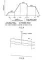
- FIGS. 1A to 1Care sectional views showing the steps of manufacturing a semiconductor device according to a first embodiment of this invention
- FIGS. 3A to 3Care sectional views showing the steps of manufacturing a semiconductor device according to a second embodiment of this invention.
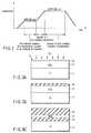
- FIG. 4is a diagram representing the temperature profile set for the heat treatment performed in the second embodiment
- FIG. 6is a schematic diagram explaining the third embodiment, depicting the relation between the substrate tilting a little and the misfit dislocation.
- FIG. 7is a sectional view showing the structure of an MOSFET device manufactured by using an SGOI substrate obtained in the third embodiment.
- an SOI substrate 10is thereby prepared, which has, as shown in FIG. 1A , a Si (SOI) layer 13 having thickness of 50 nm is formed on a Si substrate 11 having plane orientation (100) through a buried oxide film 12 .
- a thin film of SiGe alloy crystalis grow on the substrate 10 , by using a vacuum CVD apparatus. The thin film is formed at substrate temperature of 600° C., with disilane partial pressure of 20 mPa and germane partial pressure of 30 mPa.
- a SiGe layer 21 having Ge composition of 10% and thickness of 180 nmis thereby formed.
- the SiGe layer 21remains in a strained state. After the SiGe layer 21 has been grown, the supply of germane gas is stopped. The growth of the Si layer is continued at the substrate temperature of 600° C. and the disilane partial pressure of 8 mPa. A Si cap layer (protective film) 22 having thickness of 10 nm is thereby formed as uppermost layer. The SiGe layer 21 and the Si cap layer 22 are formed, one after the other, on the SOI substrate 10 having the buried oxide film 12 .
- the laminated substrate of the structure shown in FIG. 1Ais subjected to heat treatment of the temperature profile shown in FIG. 2 .
- the first thermal oxidationis performed in an oxidation furnace.
- This thermal oxidationmay be a thermal oxidation process that is employed in the ordinary method of manufacturing semiconductor devices.
- the first thermal oxidationis carried out in a dry 100%-oxygen atmosphere, at 900° C. for 60 minutes.
- the entire Si cap layer 22 and the surface region of the SiGe layer 21are oxidized as is illustrated in FIG. 1B .
- an oxide film (protective film) 23about 17 nm thick is formed on the surface of the SiGe layer on the SOI substrate.
- the SiGe layeri.e., thin film grown on the SOI substrate
- the thickness of the Si cap layeris determined by the thickness of the oxide formed by the first thermal oxidation. That is, if the oxide film is 20 nm thick, the cap layer needs to be 9 to 10 nm thick.
- the accumulation of Ge atoms in the above-mentioned interfacecan be suppressed by optimizing the thermal oxidation temperature. In this case, the Si cap layer need not be provided.
- the buried oxide film 12has grown thicker.
- the buried oxide film 12has so grown, probably because oxygen is supplied from the surface through the SiGe layer 21 .
- both oxide films 12 and 23have grown thicker and the SiGe layer 21 has become thinner, Ge atoms scarcely exist in the oxide films 12 and 23 . This is because Ge atoms expelled into the SiGe crystal layer 21 , no not taken into the thermally oxidized film 12 or 23 .
- Ge concentrationrises in the SiGe layer 21 that is interposed between the oxide films 12 and 23 .
- the lattice strain in the SiGe layer 21is relaxed.
- the thin SOI layer 13fuses with the SiGe crystal layer 21 as Ge diffuses into it from the SiGe crystal layer 21 formed on it.
- a high-temperature heat treatment(second thermal oxidation) is carried out in an oxygen-rich atmosphere.
- a buried oxide film 32is thereby formed as illustrated in FIG. 3C .
- the oxide film 23 provided on the surfacegrows thicker. Therefore, Ge concentration can rise in the SiGe layer 21 that interposed between both oxide films 23 and 32 , and the thickness of the SiGe can be decreased.
- the step of forming a buried oxide film from the oxygen-implanted layer and the step of forming an SGOI layer having high Ge concentration by means of oxidation and Ge condensationmay be performed at different times, as is illustrated in FIG. 4 . More precisely, after the first thermal oxidation is completed, the structure may be heated to 1350° C. in a non-oxidizing atmosphere, and then annealing may be continued at 1350° C. for four hours. Thereafter, the temperature may be lowered to 1200° C. and oxygen is introduced, performing the second thermal oxidation for a predetermined time.
- plane defectsi.e., slip planes that are (111) planes or similar planes, may develop. Some of these plane defects have misfit dislocation at the interface between the buried oxide film and the SGOI layer. The other plane defects are twin crystals that do not have such misfit dislocation. Since the slip planes are (111) plane or equal planes, misfit dislocations appear on ⁇ 011> axis or ⁇ 0 1 1> axis.
Landscapes
- Thin Film Transistor (AREA)
- Recrystallisation Techniques (AREA)
- Element Separation (AREA)
Abstract
Description
Claims (11)
Applications Claiming Priority (2)
| Application Number | Priority Date | Filing Date | Title |
|---|---|---|---|
| JP2005-172548 | 2005-06-13 | ||
| JP2005172548AJP4427489B2 (en) | 2005-06-13 | 2005-06-13 | Manufacturing method of semiconductor device |
Publications (2)
| Publication Number | Publication Date |
|---|---|
| US20060281234A1 US20060281234A1 (en) | 2006-12-14 |
| US7759228B2true US7759228B2 (en) | 2010-07-20 |
Family
ID=37524575
Family Applications (1)
| Application Number | Title | Priority Date | Filing Date |
|---|---|---|---|
| US11/449,687Active2028-07-10US7759228B2 (en) | 2005-06-13 | 2006-06-09 | Semiconductor device and method of manufacturing the same |
Country Status (2)
| Country | Link |
|---|---|
| US (1) | US7759228B2 (en) |
| JP (1) | JP4427489B2 (en) |
Cited By (28)
| Publication number | Priority date | Publication date | Assignee | Title |
|---|---|---|---|---|
| US20100221883A1 (en)* | 2009-02-27 | 2010-09-02 | Stephan Kronholz | Adjusting of a non-silicon fraction in a semiconductor alloy during transistor fabrication by an intermediate oxidation process |
| US20110024804A1 (en)* | 2009-07-28 | 2011-02-03 | Taiwan Semiconductor Manufacturing Company, Ltd. | Method for forming high germanium concentration sige stressor |
| US20110049613A1 (en)* | 2009-09-01 | 2011-03-03 | Taiwan Semiconductor Manufacturing Company, Ltd. | Accumulation type finfet, circuits and fabrication method thereof |
| US20110068405A1 (en)* | 2009-09-24 | 2011-03-24 | Taiwan Semiconductor Manufacturing Company, Ltd. | Fin field effect transistor |
| US8264021B2 (en) | 2009-10-01 | 2012-09-11 | Taiwan Semiconductor Manufacturing Company, Ltd. | Finfets and methods for forming the same |
| US8298925B2 (en) | 2010-11-08 | 2012-10-30 | Taiwan Semiconductor Manufacturing Company, Ltd. | Mechanisms for forming ultra shallow junction |
| US8305829B2 (en) | 2009-02-23 | 2012-11-06 | Taiwan Semiconductor Manufacturing Company, Ltd. | Memory power gating circuit for controlling internal voltage of a memory array, system and method for controlling the same |
| US8305790B2 (en) | 2009-03-16 | 2012-11-06 | Taiwan Semiconductor Manufacturing Company, Ltd. | Electrical anti-fuse and related applications |
| US8431453B2 (en) | 2011-03-31 | 2013-04-30 | Taiwan Semiconductor Manufacturing Company, Ltd. | Plasma doping to reduce dielectric loss during removal of dummy layers in a gate structure |
| US8440517B2 (en) | 2010-10-13 | 2013-05-14 | Taiwan Semiconductor Manufacturing Company, Ltd. | FinFET and method of fabricating the same |
| US8461015B2 (en) | 2009-07-08 | 2013-06-11 | Taiwan Semiconductor Manufacturing Company, Ltd. | STI structure and method of forming bottom void in same |
| US8472227B2 (en) | 2010-01-27 | 2013-06-25 | Taiwan Semiconductor Manufacturing Company, Ltd. | Integrated circuits and methods for forming the same |
| US8482073B2 (en) | 2010-03-25 | 2013-07-09 | Taiwan Semiconductor Manufacturing Company, Ltd. | Integrated circuit including FINFETs and methods for forming the same |
| US8497528B2 (en) | 2010-05-06 | 2013-07-30 | Taiwan Semiconductor Manufacturing Company, Ltd. | Method for fabricating a strained structure |
| US8592915B2 (en) | 2011-01-25 | 2013-11-26 | Taiwan Semiconductor Manufacturing Company, Ltd. | Doped oxide for shallow trench isolation (STI) |
| US8603924B2 (en) | 2010-10-19 | 2013-12-10 | Taiwan Semiconductor Manufacturing Company, Ltd. | Methods of forming gate dielectric material |
| US8629478B2 (en) | 2009-07-31 | 2014-01-14 | Taiwan Semiconductor Manufacturing Company, Ltd. | Fin structure for high mobility multiple-gate transistor |
| US8685842B2 (en) | 2010-03-31 | 2014-04-01 | Kabushiki Kaisha Toshiba | Method of manufacturing semiconductor device |
| US8759943B2 (en) | 2010-10-08 | 2014-06-24 | Taiwan Semiconductor Manufacturing Company, Ltd. | Transistor having notched fin structure and method of making the same |
| US8769446B2 (en) | 2010-11-12 | 2014-07-01 | Taiwan Semiconductor Manufacturing Company, Ltd. | Method and device for increasing fin device density for unaligned fins |
| US8877602B2 (en) | 2011-01-25 | 2014-11-04 | Taiwan Semiconductor Manufacturing Company, Ltd. | Mechanisms of doping oxide for forming shallow trench isolation |
| US8912602B2 (en) | 2009-04-14 | 2014-12-16 | Taiwan Semiconductor Manufacturing Company, Ltd. | FinFETs and methods for forming the same |
| US8957482B2 (en) | 2009-03-31 | 2015-02-17 | Taiwan Semiconductor Manufacturing Company, Ltd. | Electrical fuse and related applications |
| US8980719B2 (en) | 2010-04-28 | 2015-03-17 | Taiwan Semiconductor Manufacturing Company, Ltd. | Methods for doping fin field-effect transistors |
| US9040393B2 (en) | 2010-01-14 | 2015-05-26 | Taiwan Semiconductor Manufacturing Company, Ltd. | Method of forming semiconductor structure |
| US10252242B2 (en) | 2017-03-17 | 2019-04-09 | Air Products And Chemicals, Inc. | Alkali-promoted activated alumina adsorbent |
| WO2020051116A1 (en)* | 2018-09-03 | 2020-03-12 | Applied Materials, Inc. | Methods of forming silicon-containing layers |
| US10799849B2 (en) | 2017-03-17 | 2020-10-13 | Air Products And Chemicals, Inc. | Alkali-promoted activated alumina adsorbent |
Families Citing this family (11)
| Publication number | Priority date | Publication date | Assignee | Title |
|---|---|---|---|---|
| JP4413580B2 (en)* | 2003-11-04 | 2010-02-10 | 株式会社東芝 | Method for manufacturing element forming substrate |
| JP4427489B2 (en)* | 2005-06-13 | 2010-03-10 | 株式会社東芝 | Manufacturing method of semiconductor device |
| FR2911598B1 (en)* | 2007-01-22 | 2009-04-17 | Soitec Silicon On Insulator | SURFACE RUGOSIFICATION METHOD |
| JP5183969B2 (en)* | 2007-05-29 | 2013-04-17 | 信越半導体株式会社 | Method for forming silicon oxide film on SOI wafer |
| WO2009072984A1 (en)* | 2007-12-07 | 2009-06-11 | Agency For Science, Technology And Research | A silicon-germanium nanowire structure and a method of forming the same |
| WO2010055750A1 (en) | 2008-11-12 | 2010-05-20 | 株式会社日立製作所 | Light emitting element, light receiving element, and method for manufacturing the light receiving element |
| US8053299B2 (en) | 2009-04-17 | 2011-11-08 | Taiwan Semiconductor Manufacturing Company, Ltd. | Method of fabrication of a FinFET element |
| JP5259842B2 (en) | 2010-02-01 | 2013-08-07 | 株式会社日立製作所 | Optical element |
| JP5479304B2 (en) | 2010-11-10 | 2014-04-23 | 信越半導体株式会社 | Method for forming thermal oxide film on silicon single crystal wafer |
| CN102437129B (en)* | 2011-08-29 | 2014-09-03 | 上海华力微电子有限公司 | Localized SOI (Silicon-On-Insulator) and GOI (Germanium On Insulator) device structure and process integrating method thereof |
| FR3064398B1 (en)* | 2017-03-21 | 2019-06-07 | Soitec | SEMICONDUCTOR TYPE STRUCTURE ON INSULATION, ESPECIALLY FOR A FRONT-SIDE TYPE IMAGE SENSOR, AND METHOD FOR MANUFACTURING SUCH STRUCTURE |
Citations (18)
| Publication number | Priority date | Publication date | Assignee | Title |
|---|---|---|---|---|
| US4975387A (en)* | 1989-12-15 | 1990-12-04 | The United States Of America As Represented By The Secretary Of The Navy | Formation of epitaxial si-ge heterostructures by solid phase epitaxy |
| JP2000243946A (en) | 1998-12-24 | 2000-09-08 | Toshiba Corp | Semiconductor device and method of manufacturing semiconductor device |
| JP2002076347A (en) | 2000-08-25 | 2002-03-15 | Toshiba Corp | Semiconductor device, semiconductor substrate and method of manufacturing the same |
| US6369438B1 (en) | 1998-12-24 | 2002-04-09 | Kabushiki Kaisha Toshiba | Semiconductor device and method for manufacturing the same |
| JP2002356399A (en) | 2001-05-31 | 2002-12-13 | Mitsubishi Materials Silicon Corp | Semiconductor substrate, field effect transistor, method for forming silicon-germanium layer, method for forming strained silicon layer using the method and method for manufacturing field effect transistor |
| US20030049919A1 (en)* | 2001-09-13 | 2003-03-13 | Nec Corporation | Semiconductor device having smooth refractory metal silicide layers and process for fabrication thereof |
| US20050003229A1 (en)* | 2003-07-01 | 2005-01-06 | International Business Machines Corporation | Defect reduction by oxidation of silicon |
| US20050139961A1 (en)* | 2003-12-25 | 2005-06-30 | Siltronic Ag | Semiconductor substrate and method for production thereof |
| US20050215071A1 (en)* | 2004-03-25 | 2005-09-29 | Commissariat A L'energie Atomique | Method of preparing a silicon dioxide layer by high temperature oxidation on a substrate having, at least on the surface, germanium or a silicon-germanium alloy |
| US20060024908A1 (en)* | 2001-07-04 | 2006-02-02 | S.I.O.Tec Silicon On Insulator Technologes S.A. | Method of reducing the surface roughness of a semiconductor wafer |
| WO2006033292A1 (en) | 2004-09-24 | 2006-03-30 | Shin-Etsu Handotai Co., Ltd. | Method for manufacturing semiconductor wafer |
| US20060094171A1 (en)* | 2004-11-04 | 2006-05-04 | Taiwan Semiconductor Manufacturing Co., Ltd. | Isolation trench thermal annealing method for non-bulk silicon semiconductor substrate |
| US7084460B2 (en)* | 2003-11-03 | 2006-08-01 | International Business Machines Corporation | Method for fabricating SiGe-on-insulator (SGOI) and Ge-on-insulator (GOI) substrates |
| US20060214257A1 (en)* | 2005-03-25 | 2006-09-28 | Sumco Corporation | Production method of strained silicon-SOI substrate and strained silicon-SOI substrate produced by same |
| US20060281234A1 (en)* | 2005-06-13 | 2006-12-14 | Kabushiki Kaisha Toshiba | Semiconductor device and method of manufacturing the same |
| US20070207598A1 (en)* | 2006-03-01 | 2007-09-06 | Commissariat A L'energie Atomique | Method for producing a substrate by germanium condensation |
| US7332417B2 (en)* | 2003-01-27 | 2008-02-19 | Amberwave Systems Corporation | Semiconductor structures with structural homogeneity |
| US7501318B2 (en)* | 2003-05-30 | 2009-03-10 | International Business Machines Corporation | Formation of silicon-germanium-on-insulator (SGOI) by an integral high temperature SIMOX-Ge interdiffusion anneal |
- 2005
- 2005-06-13JPJP2005172548Apatent/JP4427489B2/ennot_activeExpired - Lifetime
- 2006
- 2006-06-09USUS11/449,687patent/US7759228B2/enactiveActive
Patent Citations (20)
| Publication number | Priority date | Publication date | Assignee | Title |
|---|---|---|---|---|
| US4975387A (en)* | 1989-12-15 | 1990-12-04 | The United States Of America As Represented By The Secretary Of The Navy | Formation of epitaxial si-ge heterostructures by solid phase epitaxy |
| JP2000243946A (en) | 1998-12-24 | 2000-09-08 | Toshiba Corp | Semiconductor device and method of manufacturing semiconductor device |
| US6369438B1 (en) | 1998-12-24 | 2002-04-09 | Kabushiki Kaisha Toshiba | Semiconductor device and method for manufacturing the same |
| JP2002076347A (en) | 2000-08-25 | 2002-03-15 | Toshiba Corp | Semiconductor device, semiconductor substrate and method of manufacturing the same |
| JP2002356399A (en) | 2001-05-31 | 2002-12-13 | Mitsubishi Materials Silicon Corp | Semiconductor substrate, field effect transistor, method for forming silicon-germanium layer, method for forming strained silicon layer using the method and method for manufacturing field effect transistor |
| US20060024908A1 (en)* | 2001-07-04 | 2006-02-02 | S.I.O.Tec Silicon On Insulator Technologes S.A. | Method of reducing the surface roughness of a semiconductor wafer |
| US20030049919A1 (en)* | 2001-09-13 | 2003-03-13 | Nec Corporation | Semiconductor device having smooth refractory metal silicide layers and process for fabrication thereof |
| US7332417B2 (en)* | 2003-01-27 | 2008-02-19 | Amberwave Systems Corporation | Semiconductor structures with structural homogeneity |
| US20080135830A1 (en)* | 2003-01-27 | 2008-06-12 | Amberwave Systems Corporation | Semiconductor structures with structural homogeneity |
| US7501318B2 (en)* | 2003-05-30 | 2009-03-10 | International Business Machines Corporation | Formation of silicon-germanium-on-insulator (SGOI) by an integral high temperature SIMOX-Ge interdiffusion anneal |
| US20050003229A1 (en)* | 2003-07-01 | 2005-01-06 | International Business Machines Corporation | Defect reduction by oxidation of silicon |
| US7084460B2 (en)* | 2003-11-03 | 2006-08-01 | International Business Machines Corporation | Method for fabricating SiGe-on-insulator (SGOI) and Ge-on-insulator (GOI) substrates |
| US20050139961A1 (en)* | 2003-12-25 | 2005-06-30 | Siltronic Ag | Semiconductor substrate and method for production thereof |
| US20050215071A1 (en)* | 2004-03-25 | 2005-09-29 | Commissariat A L'energie Atomique | Method of preparing a silicon dioxide layer by high temperature oxidation on a substrate having, at least on the surface, germanium or a silicon-germanium alloy |
| WO2006033292A1 (en) | 2004-09-24 | 2006-03-30 | Shin-Etsu Handotai Co., Ltd. | Method for manufacturing semiconductor wafer |
| US20060094171A1 (en)* | 2004-11-04 | 2006-05-04 | Taiwan Semiconductor Manufacturing Co., Ltd. | Isolation trench thermal annealing method for non-bulk silicon semiconductor substrate |
| JP2006270000A (en) | 2005-03-25 | 2006-10-05 | Sumco Corp | Manufacturing method of strained Si-SOI substrate and strained Si-SOI substrate manufactured by the method |
| US20060214257A1 (en)* | 2005-03-25 | 2006-09-28 | Sumco Corporation | Production method of strained silicon-SOI substrate and strained silicon-SOI substrate produced by same |
| US20060281234A1 (en)* | 2005-06-13 | 2006-12-14 | Kabushiki Kaisha Toshiba | Semiconductor device and method of manufacturing the same |
| US20070207598A1 (en)* | 2006-03-01 | 2007-09-06 | Commissariat A L'energie Atomique | Method for producing a substrate by germanium condensation |
Non-Patent Citations (8)
| Title |
|---|
| A Final Notice of Rejection mailed by the Japanese Patent Office on Aug. 25, 2009, for Japanese Application No. 2005-172548. |
| A Notification of Reasons for Rejection mailed by the Japanese Patent Office on May 19, 2009, for Japanese Application No. 2005-172548 with an English translation. |
| Nakaharai et al.; "Strain Relaxation Mechanism of SiGe-On-Insulator Layer in the Ge-Condensation Technique"; Proceedings of the 3rd International Conference of Si Epitaxy and Heterostructure, 3 sheets, (2003). |
| Sugiyama et al.; "Temperature Effects on Ge Condensation by Thermal Oxidation of SiGe-On-Insulator Structures"; Journal of Applied Physics, vol. 95, No. 8, pp. 4007-4011, (2004). |
| Tezuka et al.; "A Novel Fabrication Technique of Ultrathin and Relaxed SiGe Buffer Layers With High Ge Fraction for Sub-100nm Strained Silicon-On-Insulator MOSFETs"; Japanese Journal of Applied Physics, vol. 40, pp. 2866-2874, (2001). |
| Tezuka et al.; "Fabrication of Strained Si on an Ultrathin SiGe-On-Insulator Virtual Substrate With a High-Ge Fraction"; Applied Physics Letters, vol. 79, No. 12, pp. 1798-1800, (Sep. 2001). |
| Tezuka et al.; "Lattice Relaxation and Dislocation Generation/Annihilation in SiGe-On-Insulator Layers During Ge Condensation Process"; Proceeding of the 4th Intenrnational Conference of Si Epitaxy and Heterostructure, 2 sheets, (2005). |
| Waltereit, P. et al., "Si/SiGe quantum wells grown on vicinal Si(001) substrates: Morphology, dislocation dynamics, and transport properties" Applied Physics letters, vol. 72, No. 18, May 4, 1998. |
Cited By (53)
| Publication number | Priority date | Publication date | Assignee | Title |
|---|---|---|---|---|
| US8305829B2 (en) | 2009-02-23 | 2012-11-06 | Taiwan Semiconductor Manufacturing Company, Ltd. | Memory power gating circuit for controlling internal voltage of a memory array, system and method for controlling the same |
| US20100221883A1 (en)* | 2009-02-27 | 2010-09-02 | Stephan Kronholz | Adjusting of a non-silicon fraction in a semiconductor alloy during transistor fabrication by an intermediate oxidation process |
| US8735253B2 (en)* | 2009-02-27 | 2014-05-27 | Globalfoundries Inc. | Adjusting of a non-silicon fraction in a semiconductor alloy during transistor fabrication by an intermediate oxidation process |
| US8305790B2 (en) | 2009-03-16 | 2012-11-06 | Taiwan Semiconductor Manufacturing Company, Ltd. | Electrical anti-fuse and related applications |
| US8957482B2 (en) | 2009-03-31 | 2015-02-17 | Taiwan Semiconductor Manufacturing Company, Ltd. | Electrical fuse and related applications |
| US8912602B2 (en) | 2009-04-14 | 2014-12-16 | Taiwan Semiconductor Manufacturing Company, Ltd. | FinFETs and methods for forming the same |
| US8461015B2 (en) | 2009-07-08 | 2013-06-11 | Taiwan Semiconductor Manufacturing Company, Ltd. | STI structure and method of forming bottom void in same |
| US8623728B2 (en)* | 2009-07-28 | 2014-01-07 | Taiwan Semiconductor Manufacturing Company, Ltd. | Method for forming high germanium concentration SiGe stressor |
| US20110024804A1 (en)* | 2009-07-28 | 2011-02-03 | Taiwan Semiconductor Manufacturing Company, Ltd. | Method for forming high germanium concentration sige stressor |
| US9660082B2 (en) | 2009-07-28 | 2017-05-23 | Taiwan Semiconductor Manufacturing Company, Ltd. | Integrated circuit transistor structure with high germanium concentration SiGe stressor |
| US8629478B2 (en) | 2009-07-31 | 2014-01-14 | Taiwan Semiconductor Manufacturing Company, Ltd. | Fin structure for high mobility multiple-gate transistor |
| US8264032B2 (en) | 2009-09-01 | 2012-09-11 | Taiwan Semiconductor Manufacturing Company, Ltd. | Accumulation type FinFET, circuits and fabrication method thereof |
| US20110049613A1 (en)* | 2009-09-01 | 2011-03-03 | Taiwan Semiconductor Manufacturing Company, Ltd. | Accumulation type finfet, circuits and fabrication method thereof |
| US11158725B2 (en) | 2009-09-24 | 2021-10-26 | Taiwan Semiconductor Manufacturing Company, Ltd. | Fin structure of fin field effect transistor |
| US20110068405A1 (en)* | 2009-09-24 | 2011-03-24 | Taiwan Semiconductor Manufacturing Company, Ltd. | Fin field effect transistor |
| US10355108B2 (en) | 2009-09-24 | 2019-07-16 | Taiwan Semiconductor Manufacturing Company, Ltd. | Method of forming a fin field effect transistor comprising two etching steps to define a fin structure |
| US9484462B2 (en) | 2009-09-24 | 2016-11-01 | Taiwan Semiconductor Manufacturing Company, Ltd. | Fin structure of fin field effect transistor |
| US8264021B2 (en) | 2009-10-01 | 2012-09-11 | Taiwan Semiconductor Manufacturing Company, Ltd. | Finfets and methods for forming the same |
| US9040393B2 (en) | 2010-01-14 | 2015-05-26 | Taiwan Semiconductor Manufacturing Company, Ltd. | Method of forming semiconductor structure |
| US9922827B2 (en) | 2010-01-14 | 2018-03-20 | Taiwan Semiconductor Manufacturing Company, Ltd. | Method of forming a semiconductor structure |
| US8472227B2 (en) | 2010-01-27 | 2013-06-25 | Taiwan Semiconductor Manufacturing Company, Ltd. | Integrated circuits and methods for forming the same |
| US8482073B2 (en) | 2010-03-25 | 2013-07-09 | Taiwan Semiconductor Manufacturing Company, Ltd. | Integrated circuit including FINFETs and methods for forming the same |
| US8685842B2 (en) | 2010-03-31 | 2014-04-01 | Kabushiki Kaisha Toshiba | Method of manufacturing semiconductor device |
| US9450097B2 (en) | 2010-04-28 | 2016-09-20 | Taiwan Semiconductor Manufacturing Company, Ltd. | Methods for doping Fin field-effect transistors and Fin field-effect transistor |
| US9209280B2 (en) | 2010-04-28 | 2015-12-08 | Taiwan Semiconductor Manufacturing Company, Ltd. | Methods for doping fin field-effect transistors |
| US8980719B2 (en) | 2010-04-28 | 2015-03-17 | Taiwan Semiconductor Manufacturing Company, Ltd. | Methods for doping fin field-effect transistors |
| US11855210B2 (en) | 2010-05-06 | 2023-12-26 | Taiwan Semiconductor Manufacturing Company, Ltd. | Method for fabricating a strained structure and structure formed |
| US9564529B2 (en) | 2010-05-06 | 2017-02-07 | Taiwan Semiconductor Manufacturing Company, Ltd. | Method for fabricating a strained structure and structure formed |
| US12356674B2 (en) | 2010-05-06 | 2025-07-08 | Taiwan Semiconductor Manufacturing Company, Ltd. | Method for fabricating a strained structure and structure formed |
| US10510887B2 (en) | 2010-05-06 | 2019-12-17 | Taiwan Semiconductor Manufacturing Company, Ltd. | Method for fabricating a strained structure and structure formed |
| US11251303B2 (en) | 2010-05-06 | 2022-02-15 | Taiwan Semiconductor Manufacturing Company, Ltd. | Method for fabricating a strained structure and structure formed |
| US9147594B2 (en) | 2010-05-06 | 2015-09-29 | Taiwan Semiconductor Manufacturing Company, Ltd. | Method for fabricating a strained structure |
| US10998442B2 (en) | 2010-05-06 | 2021-05-04 | Taiwan Semiconductor Manufacturing Company, Ltd. | Method for fabricating a strained structure and structure formed |
| US8497528B2 (en) | 2010-05-06 | 2013-07-30 | Taiwan Semiconductor Manufacturing Company, Ltd. | Method for fabricating a strained structure |
| US8759943B2 (en) | 2010-10-08 | 2014-06-24 | Taiwan Semiconductor Manufacturing Company, Ltd. | Transistor having notched fin structure and method of making the same |
| US9716091B2 (en) | 2010-10-13 | 2017-07-25 | Taiwan Semiconductor Manufacturing Company, Ltd. | Fin field effect transistor |
| US8809940B2 (en) | 2010-10-13 | 2014-08-19 | Taiwan Semiconductor Manufacturing Company, Ltd. | Fin held effect transistor |
| US9209300B2 (en) | 2010-10-13 | 2015-12-08 | Taiwan Semiconductor Manufacturing Company, Ltd. | Fin field effect transistor |
| US8440517B2 (en) | 2010-10-13 | 2013-05-14 | Taiwan Semiconductor Manufacturing Company, Ltd. | FinFET and method of fabricating the same |
| US9893160B2 (en) | 2010-10-19 | 2018-02-13 | Taiwan Semiconductor Manufacturing Company, Ltd. | Methods of forming gate dielectric material |
| US8603924B2 (en) | 2010-10-19 | 2013-12-10 | Taiwan Semiconductor Manufacturing Company, Ltd. | Methods of forming gate dielectric material |
| US8298925B2 (en) | 2010-11-08 | 2012-10-30 | Taiwan Semiconductor Manufacturing Company, Ltd. | Mechanisms for forming ultra shallow junction |
| US8769446B2 (en) | 2010-11-12 | 2014-07-01 | Taiwan Semiconductor Manufacturing Company, Ltd. | Method and device for increasing fin device density for unaligned fins |
| US8806397B2 (en) | 2010-11-12 | 2014-08-12 | Taiwan Semiconductor Manufacturing Company, Ltd. | Method and device for increasing fin device density for unaligned fins |
| US9026959B2 (en) | 2010-11-12 | 2015-05-05 | Taiwan Semiconductor Manufacturing Company, Ltd. | Method and device for increasing fin device density for unaligned fins |
| US8592915B2 (en) | 2011-01-25 | 2013-11-26 | Taiwan Semiconductor Manufacturing Company, Ltd. | Doped oxide for shallow trench isolation (STI) |
| US9184088B2 (en) | 2011-01-25 | 2015-11-10 | Taiwan Semiconductor Manufacturing Company, Ltd. | Method of making a shallow trench isolation (STI) structures |
| US8877602B2 (en) | 2011-01-25 | 2014-11-04 | Taiwan Semiconductor Manufacturing Company, Ltd. | Mechanisms of doping oxide for forming shallow trench isolation |
| US8431453B2 (en) | 2011-03-31 | 2013-04-30 | Taiwan Semiconductor Manufacturing Company, Ltd. | Plasma doping to reduce dielectric loss during removal of dummy layers in a gate structure |
| US10799849B2 (en) | 2017-03-17 | 2020-10-13 | Air Products And Chemicals, Inc. | Alkali-promoted activated alumina adsorbent |
| US10252242B2 (en) | 2017-03-17 | 2019-04-09 | Air Products And Chemicals, Inc. | Alkali-promoted activated alumina adsorbent |
| WO2020051116A1 (en)* | 2018-09-03 | 2020-03-12 | Applied Materials, Inc. | Methods of forming silicon-containing layers |
| TWI753297B (en)* | 2018-09-03 | 2022-01-21 | 美商應用材料股份有限公司 | Methods of forming silicon-containing layers |
Also Published As
| Publication number | Publication date |
|---|---|
| JP4427489B2 (en) | 2010-03-10 |
| JP2006351612A (en) | 2006-12-28 |
| US20060281234A1 (en) | 2006-12-14 |
Similar Documents
| Publication | Publication Date | Title |
|---|---|---|
| US7759228B2 (en) | Semiconductor device and method of manufacturing the same | |
| KR100392166B1 (en) | Semiconductor device and method for manufacturing the same | |
| US6723541B2 (en) | Method of producing semiconductor device and semiconductor substrate | |
| US7226833B2 (en) | Semiconductor device structure and method therefor | |
| TWI407563B (en) | Low defect SI with reverse carbon distribution: C layer | |
| EP0085434B1 (en) | Semiconductor devices and method for making the same | |
| US7557018B2 (en) | Element fabrication substrate | |
| US7416959B2 (en) | Silicon-on-insulator semiconductor wafer | |
| TWI236707B (en) | Manufacturing method of semiconductor substrate | |
| JP2004014856A (en) | Method for manufacturing semiconductor substrate and method for manufacturing semiconductor device | |
| JPH10308513A (en) | Method of forming a heterojunction semiconductor device having a strained layer | |
| JPS63142655A (en) | Manufacture of device containing buried sio2 layer | |
| JP2006524426A (en) | Method and layer structure for producing strained layers on a substrate | |
| US7037806B1 (en) | Method of fabricating silicon-on-insulator semiconductor substrate using rare earth oxide or rare earth nitride | |
| JP4212228B2 (en) | Manufacturing method of semiconductor device | |
| US20080164572A1 (en) | Semiconductor substrate and manufacturing method thereof | |
| US6869897B2 (en) | Manufacturing method for semiconductor substrate, and semiconductor device having a strained Si layer | |
| US7345329B2 (en) | Method for reduced N+ diffusion in strained Si on SiGe substrate | |
| JP2005236272A (en) | Low temperature annealing to reduce defects in SiXGe1-X layer with relaxed hydrogen implantation | |
| JP2009512185A (en) | Semiconductor SOI device | |
| JP3660469B2 (en) | Manufacturing method of SOI substrate | |
| US6911380B2 (en) | Method of forming silicon on insulator wafers | |
| CN1322547C (en) | Process for preparing silicon-germanium material on insulator based on silicon-germanium / silicon structure separation-by-implantation-of-oxygen | |
| JP3810168B2 (en) | Manufacturing method of semiconductor substrate | |
| JP3091800B2 (en) | Method for manufacturing SOI substrate |
Legal Events
| Date | Code | Title | Description |
|---|---|---|---|
| AS | Assignment | Owner name:KABUSHIKI KAISHA TOSHIBA, JAPAN Free format text:ASSIGNMENT OF ASSIGNORS INTEREST;ASSIGNORS:SUGIYAMA, NAOHARU;HIRASHITA, NORIO;TEZUKA, TSUTOMU;REEL/FRAME:017989/0751 Effective date:20060525 Owner name:OKI ELECTRIC INDUSTRY CO., LTD., JAPAN Free format text:ASSIGNMENT OF ASSIGNORS INTEREST;ASSIGNORS:SUGIYAMA, NAOHARU;HIRASHITA, NORIO;TEZUKA, TSUTOMU;REEL/FRAME:017989/0751 Effective date:20060525 | |
| AS | Assignment | Owner name:OKI SEMICONDUCTOR CO., LTD., JAPAN Free format text:CHANGE OF NAME;ASSIGNOR:OKI ELECTRIC INDUSTRY CO., LTD.;REEL/FRAME:022162/0586 Effective date:20081001 Owner name:OKI SEMICONDUCTOR CO., LTD.,JAPAN Free format text:CHANGE OF NAME;ASSIGNOR:OKI ELECTRIC INDUSTRY CO., LTD.;REEL/FRAME:022162/0586 Effective date:20081001 | |
| STCF | Information on status: patent grant | Free format text:PATENTED CASE | |
| CC | Certificate of correction | ||
| FEPP | Fee payment procedure | Free format text:PAYOR NUMBER ASSIGNED (ORIGINAL EVENT CODE: ASPN); ENTITY STATUS OF PATENT OWNER: LARGE ENTITY | |
| FPAY | Fee payment | Year of fee payment:4 | |
| AS | Assignment | Owner name:LAPIS SEMICONDUCTOR CO., LTD., JAPAN Free format text:CHANGE OF NAME;ASSIGNOR:OKI SEMICONDUCTOR CO., LTD;REEL/FRAME:032495/0483 Effective date:20111003 | |
| MAFP | Maintenance fee payment | Free format text:PAYMENT OF MAINTENANCE FEE, 8TH YEAR, LARGE ENTITY (ORIGINAL EVENT CODE: M1552) Year of fee payment:8 | |
| MAFP | Maintenance fee payment | Free format text:PAYMENT OF MAINTENANCE FEE, 12TH YEAR, LARGE ENTITY (ORIGINAL EVENT CODE: M1553); ENTITY STATUS OF PATENT OWNER: LARGE ENTITY Year of fee payment:12 |