US7757061B2 - System and method for decoding commands based on command signals and operating state - Google Patents
System and method for decoding commands based on command signals and operating stateDownload PDFInfo
- Publication number
- US7757061B2 US7757061B2US11/121,868US12186805AUS7757061B2US 7757061 B2US7757061 B2US 7757061B2US 12186805 AUS12186805 AUS 12186805AUS 7757061 B2US7757061 B2US 7757061B2
- Authority
- US
- United States
- Prior art keywords
- command
- state
- memory
- signals
- operating state
- Prior art date
- Legal status (The legal status is an assumption and is not a legal conclusion. Google has not performed a legal analysis and makes no representation as to the accuracy of the status listed.)
- Active, expires
Links
Images


Classifications
- G—PHYSICS
- G06—COMPUTING OR CALCULATING; COUNTING
- G06F—ELECTRIC DIGITAL DATA PROCESSING
- G06F9/00—Arrangements for program control, e.g. control units
- G06F9/06—Arrangements for program control, e.g. control units using stored programs, i.e. using an internal store of processing equipment to receive or retain programs
- G06F9/30—Arrangements for executing machine instructions, e.g. instruction decode
- G—PHYSICS
- G11—INFORMATION STORAGE
- G11C—STATIC STORES
- G11C11/00—Digital stores characterised by the use of particular electric or magnetic storage elements; Storage elements therefor
- G11C11/21—Digital stores characterised by the use of particular electric or magnetic storage elements; Storage elements therefor using electric elements
- G11C11/34—Digital stores characterised by the use of particular electric or magnetic storage elements; Storage elements therefor using electric elements using semiconductor devices
- G11C11/40—Digital stores characterised by the use of particular electric or magnetic storage elements; Storage elements therefor using electric elements using semiconductor devices using transistors
- G11C11/401—Digital stores characterised by the use of particular electric or magnetic storage elements; Storage elements therefor using electric elements using semiconductor devices using transistors forming cells needing refreshing or charge regeneration, i.e. dynamic cells
- G11C11/4063—Auxiliary circuits, e.g. for addressing, decoding, driving, writing, sensing or timing
- G11C11/407—Auxiliary circuits, e.g. for addressing, decoding, driving, writing, sensing or timing for memory cells of the field-effect type
- G11C11/409—Read-write [R-W] circuits
- G11C11/4096—Input/output [I/O] data management or control circuits, e.g. reading or writing circuits, I/O drivers or bit-line switches
- G—PHYSICS
- G11—INFORMATION STORAGE
- G11C—STATIC STORES
- G11C11/00—Digital stores characterised by the use of particular electric or magnetic storage elements; Storage elements therefor
- G11C11/21—Digital stores characterised by the use of particular electric or magnetic storage elements; Storage elements therefor using electric elements
- G11C11/34—Digital stores characterised by the use of particular electric or magnetic storage elements; Storage elements therefor using electric elements using semiconductor devices
- G11C11/40—Digital stores characterised by the use of particular electric or magnetic storage elements; Storage elements therefor using electric elements using semiconductor devices using transistors
- G11C11/401—Digital stores characterised by the use of particular electric or magnetic storage elements; Storage elements therefor using electric elements using semiconductor devices using transistors forming cells needing refreshing or charge regeneration, i.e. dynamic cells
- G11C11/406—Management or control of the refreshing or charge-regeneration cycles
- G11C11/40611—External triggering or timing of internal or partially internal refresh operations, e.g. auto-refresh or CAS-before-RAS triggered refresh
- G—PHYSICS
- G11—INFORMATION STORAGE
- G11C—STATIC STORES
- G11C11/00—Digital stores characterised by the use of particular electric or magnetic storage elements; Storage elements therefor
- G11C11/21—Digital stores characterised by the use of particular electric or magnetic storage elements; Storage elements therefor using electric elements
- G11C11/34—Digital stores characterised by the use of particular electric or magnetic storage elements; Storage elements therefor using electric elements using semiconductor devices
- G11C11/40—Digital stores characterised by the use of particular electric or magnetic storage elements; Storage elements therefor using electric elements using semiconductor devices using transistors
- G11C11/401—Digital stores characterised by the use of particular electric or magnetic storage elements; Storage elements therefor using electric elements using semiconductor devices using transistors forming cells needing refreshing or charge regeneration, i.e. dynamic cells
- G11C11/4063—Auxiliary circuits, e.g. for addressing, decoding, driving, writing, sensing or timing
- G11C11/407—Auxiliary circuits, e.g. for addressing, decoding, driving, writing, sensing or timing for memory cells of the field-effect type
- G11C11/4076—Timing circuits
- G—PHYSICS
- G11—INFORMATION STORAGE
- G11C—STATIC STORES
- G11C11/00—Digital stores characterised by the use of particular electric or magnetic storage elements; Storage elements therefor
- G11C11/21—Digital stores characterised by the use of particular electric or magnetic storage elements; Storage elements therefor using electric elements
- G11C11/34—Digital stores characterised by the use of particular electric or magnetic storage elements; Storage elements therefor using electric elements using semiconductor devices
- G11C11/40—Digital stores characterised by the use of particular electric or magnetic storage elements; Storage elements therefor using electric elements using semiconductor devices using transistors
- G11C11/401—Digital stores characterised by the use of particular electric or magnetic storage elements; Storage elements therefor using electric elements using semiconductor devices using transistors forming cells needing refreshing or charge regeneration, i.e. dynamic cells
- G11C11/4063—Auxiliary circuits, e.g. for addressing, decoding, driving, writing, sensing or timing
- G11C11/407—Auxiliary circuits, e.g. for addressing, decoding, driving, writing, sensing or timing for memory cells of the field-effect type
- G11C11/408—Address circuits
- G11C11/4087—Address decoders, e.g. bit - or word line decoders; Multiple line decoders
- G—PHYSICS
- G11—INFORMATION STORAGE
- G11C—STATIC STORES
- G11C11/00—Digital stores characterised by the use of particular electric or magnetic storage elements; Storage elements therefor
- G11C11/21—Digital stores characterised by the use of particular electric or magnetic storage elements; Storage elements therefor using electric elements
- G11C11/34—Digital stores characterised by the use of particular electric or magnetic storage elements; Storage elements therefor using electric elements using semiconductor devices
- G11C11/40—Digital stores characterised by the use of particular electric or magnetic storage elements; Storage elements therefor using electric elements using semiconductor devices using transistors
- G11C11/401—Digital stores characterised by the use of particular electric or magnetic storage elements; Storage elements therefor using electric elements using semiconductor devices using transistors forming cells needing refreshing or charge regeneration, i.e. dynamic cells
- G11C11/4063—Auxiliary circuits, e.g. for addressing, decoding, driving, writing, sensing or timing
- G11C11/407—Auxiliary circuits, e.g. for addressing, decoding, driving, writing, sensing or timing for memory cells of the field-effect type
- G11C11/409—Read-write [R-W] circuits
- G11C11/4091—Sense or sense/refresh amplifiers, or associated sense circuitry, e.g. for coupled bit-line precharging, equalising or isolating
- G—PHYSICS
- G11—INFORMATION STORAGE
- G11C—STATIC STORES
- G11C7/00—Arrangements for writing information into, or reading information out from, a digital store
- G11C7/10—Input/output [I/O] data interface arrangements, e.g. I/O data control circuits, I/O data buffers
- G11C7/1072—Input/output [I/O] data interface arrangements, e.g. I/O data control circuits, I/O data buffers for memories with random access ports synchronised on clock signal pulse trains, e.g. synchronous memories, self timed memories
Definitions
- the inventionrelates generally to command decoding for a memory system, and more particularly, to decoding command signals to perform operations in the memory system based on the command signals and a operating state of the memory system.
- Computer systemsuse memory devices, such as synchronous dynamic random access memory (“SDRAM”) devices, to store instructions and data that are access by a processor. These memory devices are normally used as system memory in a computer system.
- the processorcommunicates with the system memory through a processor bus and a memory controller.
- the processorissues a memory request, which includes a memory command, such as a read command, and an address designating the location from which data or instructions are to be read.
- the memory controlleruses the command and address to generate appropriate command signals as well as row and column addresses, which are applied to the system memory.
- datais transferred between the system memory and the processor.
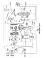
- FIG. 1is a functional block diagram of a conventional memory device 100 .
- the memory device 100 in FIG. 1is an example of a double-data rate (DDR) SDRAM.
- the memory device 100is referred to as a double-data-rate device because the data words DQ being transferred to and from the device are transferred at double the rate of a conventional SDRAM, which transfers data at a rate corresponding to the frequency of the applied clock signal.
- the memory device 100includes a control logic and command decoder 134 that receives a plurality of command and clock signals over a control bus CONT, typically from an external circuit such as a memory controller (not shown).
- the command signalsinclude a chip select signal CS#, a write enable signal WE#, a column address strobe signal CAS#, and a row address strobe signal RAS#, while the clock signals include a clock enable signal CKE# and complementary clock signals CLK, CLK#, with the “#” designating a signal as being active LOW.
- the command signals RAS#, CAS#, and WE#are driven to values corresponding to a particular command, such as a read, write, or auto-refresh command.
- the command decoder 134In response to the clock signals CLK, CLK#, the command decoder 134 latches and decodes an applied command, and generates a sequence of internal clock and control signals that control the components 102 - 132 to execute the function of the applied command.
- the clock enable signal CKEenables clocking of the command decoder 134 by the clock signals CLK, CLK#.
- the command decoder 134further includes mode registers 136 . Data written to the mode registers 136 are used to set various modes of operation, for example, burst data length, burst type, power-down mode, CAS latency, and the like.
- the command decoder 134will generate the appropriate internal clock and control signals based on the modes set by the data stored in the mode registers 136 .
- the bank control logic 106activates the row address latch and decoder 110 A-D corresponding to either the bank address received from the address register 102 or a refresh bank address from the refresh counter 108 , and the activated row address latch and decoder latches and decodes the received row address.
- the activated row address latch and decoder 110 A-Dapplies various signals to a corresponding memory bank 112 A-D to thereby activate a row of memory cells corresponding to the decoded row address.
- Each memory bank 112 A-Dincludes a memory-cell array having a plurality of memory cells arranged in rows and columns, and the data stored in the memory cells in the activated row is stored in sense amplifiers in the corresponding memory bank.
- the row address multiplexer 104applies the refresh row address from the refresh counter 108 to the decoders 110 A-D and the bank control logic circuit 106 uses the refresh bank address from the refresh counter when the memory device 100 operates in an auto-refresh or self-refresh mode of operation in response to an auto- or self-refresh command being applied to the memory device 100 , as will be appreciated by those skilled in the art.
- a column addressis applied on the ADDR bus after the row and bank addresses, and the address register 102 applies the column address to a column address counter and latch 114 which, in turn, latches the column address and applies the latched column address to a plurality of column decoders 116 A-D.
- the bank control logic 106activates the column decoder 116 A-D corresponding to the received bank address, and the activated column decoder decodes the applied column address.
- the column address counter and latch 114either directly applies the latched column address to the decoders 116 A-D, or applies a sequence of column addresses to the decoders starting at the column address provided by the address register 102 .
- data being read from the addressed memory cellsis coupled through the I/O gating and data masking circuit 118 to a read latch 120 .
- the I/O gating and data masking circuit 118supplies N bits of data to the read latch 120 , which then applies two N/4 bit words to a multiplexer 122 .
- the circuit 118provides 32 bits to the read latch 120 which, in turn, provides four 8 bits words to the multiplexer 122 .
- a data driver 124sequentially receives the N/4 bit words from the multiplexer 122 and also receives a data strobe signal DQS from a strobe signal generator 126 and a delayed clock signal CLKDEL from the delay-locked loop 123 .
- the DQS signalis used by an external circuit such as a memory controller (not shown) in latching data from the memory device 100 during read operations.
- the data driver 124sequentially outputs the received N/4 bits words as a corresponding data word DQ, each data word being output in synchronism with a rising or falling edge of a CLK signal that is applied to clock the memory device 100 .
- the data driver 124also outputs the data strobe signal DQS having rising and falling edges in synchronism with rising and falling edges of the CLK signal, respectively.
- Each data word DQ and the data strobe signal DQScollectively define a data bus DATA.
- the DATA busalso includes masking signals DM 0 -M for masking write data of data write operations, as will be described in more detail below.
- an external circuitsuch as a memory controller (not shown) applies N/4 bit data words DQ, the strobe signal DQS, and corresponding data masking signals DM on the data bus DATA.
- a data receiver 128receives each DQ word and the associated DM signals, and applies these signals to input registers 130 that are clocked by the DQS signal. In response to a rising edge of the DQS signal, the input registers 130 latch a first N/4 bit DQ word and the associated DM signals, and in response to a falling edge of the DQS signal the input registers latch the second N/4 bit DQ word and associated DM signals.
- the input register 130provides the two latched N/4 bit DQ words as an N-bit word to a write FIFO and driver 132 , which clocks the applied DQ word and DM signals into the write FIFO and driver in response to the DQS signal.
- the DQ wordis clocked out of the write FIFO and driver 132 in response to the CLK signal, and is applied to the I/O gating and masking circuit 118 .
- the I/O gating and masking circuit 118transfers the DQ word to the addressed memory cells in the accessed bank 112 A-D subject to the DM signals, which may be used to selectively mask bits or groups of bits in the DQ words (i.e., in the write data) being written to the addressed memory cells.
- commandsare issued to the memory device 100 in the form of command signals, which are decoded by the command decoder 134 to generate internal clock and control signals to perform the requested operation.
- FIG. 2is a command decoding truth table for the memory device 100 .
- the three command signals RAS#, CAS#, and WE#provide eight different commands for the memory device 100 . These commands include LOAD MODE, REFRESH, PRECHARGE, BANK ACTIVATE, WRITE, READ, NOP (no operation), and a RESERVED command, which can be used in the future for an additional command.
- the LOAD MODE commandis used to load data into the mode registers 136 , which, as previously discussed, is used to set various modes of operation, for example, burst data length, burst type, power-down mode, CAS latency, and the like.
- the REFRESH commandis used to invoke a refresh sequence in the memory banks 112 A-D.
- the PRECHARGE commandis used to deactivate or “close” activated, or “open,” memory banks 112 A-D.
- the BANK ACTIVATE commandis used to open at least one of the memory banks 112 A-D, as selected by a bank address, in preparation for an memory access operation.
- the WRITE command and the READ commandare used to invoke a data write operation and a data read operation, respectively, as previously described.
- the NOP operationis used to prevent unwanted commands from being registered during idle or wait states of the memory device 100 .
- the use of the RAS#, CAS#, and WE# signalsprovides an effective way to issue commands to the memory device 100 .
- One such limitationis the maximum number of different possible commands that are provided with the conventional command decoding of the memory device 100 .
- the three command signalsprovide a maximum decoding of eight different commands. Although eight different commands are sufficient for current technology, it is easy to imagine that in the future there may be the need for more than the eight commands previously described. If additional commands are desired, additional command signals will need to be used. For example, if two additional commands for a total of ten commands are desired, one command could be decoded using the RESERVED command. However, the other additional command would require adding one more signal to the existing three commands signals. With four command signals, there are now potentially sixteen different commands that can be decoded.
- Embodiments of the present inventionare directed to a system and method for decoding command signals.
- a command decoderis configured to generate internal control signals to perform an operation selected from a first set of operations according to the latched logic levels of the command signals when the memory system is in a first operating state.
- the command decoderis further configured to generate internal control signals to perform an operation selected from a second set of operations according to the latched logic levels of the command signals when the memory system is in a second operating state.
- a method of decoding command signalsincludes receiving command signals, and selecting one operation from a first set of operations in accordance with the command signals while the memory system is in a first operating state, and selecting one operation from a second set of operations in accordance with the command signals while the memory system is in a second operating state.
- FIG. 1is a functional block diagram of a memory system having conventional command decoding.
- FIG. 2is a truth table of conventional command decoding utilized in the memory system of FIG. 1 .
- FIG. 3is a functional block diagram of a memory system having command decoding according to an embodiment of the present invention.
- FIG. 4is a truth table of the command decoding utilized in the memory system of FIG. 3 according to an embodiment of the present invention.
- FIG. 5is a state diagram for the command decoding shown in the truth table of FIG. 4 .
- FIG. 6is a truth table of command decoding that can be utilized in the memory system of FIG. 3 according to an alternative embodiment of the present invention.
- FIG. 7is a state diagram for command decoding that can be utilized in the memory system of FIG. 3 according to an alternative embodiment of the present invention.
- FIG. 8is a functional block diagram of a processing system including a memory system having command decoding according to an embodiment of the present invention.
- Embodiments of the present inventionprovide systems and methods for command decoding in a memory that decodes commands based on command signals in combination with an operating state of the memory. Certain details are set forth below to provide a sufficient understanding of the invention. However, it will be clear to one skilled in the art that the invention may be practiced without these particular details. In other instances, well-known circuits, control signals, timing protocols, and software operations have not been shown in detail in order to avoid unnecessarily obscuring the invention.
- FIG. 3illustrates a memory device 300 having control logic and command decoder 334 according to an embodiment of the present invention.
- Many of the circuits included in the memory device 300have been previously described with respect to the memory device 100 of FIG. 1 , and consequently, in the interest of brevity, will not be described again. Operation of these circuits in the memory device 300 are the same as in previously described with respect to the memory device 100 of FIG. 1 , and are referenced in FIG. 3 using the same reference number.
- the command decoder 334is different than the command decoder 134 of the memory device 100 .
- the command decoder 334decodes command signals applied to the memory device 300 and generates internal clock and control signals to execute the requested command based on the command signals in combination with a operating state of the memory device 300 .
- the command decoder 334generates the internal signals to perform a requested operation based on the set of command signals applied to the memory device 300 and its current operating state.
- the number of command signals needed for decoding the commandscan be reduced while maintaining the same number of different commands available.
- the number of different commandscan be increased without increasing the number of command signals.
- the memory device 300has the same number of commands as previously described for the memory device 100 , and shown in the table of FIG. 2 .
- the eight different commandsare LOAD MODE REGISTERS, REFRESH, PRECHARGE, BANK ACTIVATE, WRITE, READ, RESERVED, and NOP.
- These eight commands for the memory device 100can be selected based on the combination of the logic states of the three command signals RAS#, CAS#, and WE#.
- the memory device 300can select one of the same eight commands using only two command signals, RAS# and WE#, in combination with monitoring a bank active state.
- the command decoder 334is coupled to the bank control logic 306 to receive a bank active state signal BACTIVE having a logic state indicative of whether any of the memory banks 112 A-D are “open” (i.e., active) or if all of the banks are “closed” (i.e., precharged).
- FIG. 4illustrates a truth table for command decoding in the memory device 300 of FIG. 3 according to an embodiment of the present invention.
- Column 402lists the commands for different combinations of the RAS# and WE# signals when any of the memory banks 312 A-D are open.
- Column 404lists the commands for different combinations of the RAS# and WE# signals for when all of the memory banks 312 A-D are closed.
- the command decoder 334will generate internal clock and control signals to execute a WRITE operation to at least one memory location in the memory banks 312 A-D identified by the address and bank signals, as previously described.
- the command decoder 334will generate internal clock and control signals to execute a LOAD MODE command that loads mode information into the mode register 136 , as previously described.
- the memory device 300has the same eight commands as the memory device 100 , but only requires the two RAS# and WE# signals instead of the three RAS#, CAS#, and WE# signals.
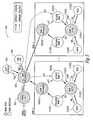
- FIG. 5is a state diagram illustrating the command decoding of the memory device 300 as previously described with respect to the command decoding truth table of FIG. 4 .
- FIG. 5illustrates various memory device operations, represented by circles, and various memory device states, represented by shaded circles.
- the memory device 300changes states and performs operations in response to command signals RAS# and WE#, with command sequences (defined by a combination of command signals) and changes of state represented by arrows pointing from a memory device state to a memory device operation.
- Bold arrows in FIG. 5represent an automatic sequence that returns the memory device 300 to a memory device state upon completion of the memory device operation.
- FIG. 5illustrates various memory device operations, represented by circles, and various memory device states, represented by shaded circles.
- the memory device 300changes states and performs operations in response to command signals RAS# and WE#, with command sequences (defined by a combination of command signals) and changes of state represented by arrows pointing from a memory device state to a memory device operation.
- FIG. 5illustrates command decoding on a per bank basis for memory banks 0 to N, which correspond to the memory banks 112 A-D of the memory device 300 .
- Memory bank selectionis made by way of bank addresses applied to the memory device at the time the command signals are latched.
- a power-on sequenceis executed to place the memory device 300 in a POWER ON state 502 .
- the memory device 300exits the POWER ON state 502 and is reset to an ALL BANK PRECHARGED state 504 .
- ALL BANK PRECHARGED state 504While in the ALL BANK PRECHARGED state 504 and all of the memory banks 112 A-D are closed, application of the RAS# and WE# signals are be decoded by the command decoder 334 into one of three commands (not including the RESERVED command). The three commands shown in FIG.
- REFRESH commandthat causes the memory device 300 to execute an AUTO REFRESH operation 506
- LOAD MODE commandthat causes the memory device 300 to execute an LOAD MRS operation 508
- BANK ACTIVATE commandthat causes the memory device 300 to execute an ACTIVATE BANK command 509 for a particular memory bank 0 through N.
- the REFRESH commandis decoded from a LOW RAS# signal and a LOW WE# signal applied to the command decoder 334 while the memory device 300 is in the ALL BANK PRECHARGED state 504 .
- the memory device 300changes from the ALL BANK PRECHARGED state 504 to execute the AUTO REFRESH sequence 506 .
- the AUTO REFRESH sequence 506is completed, the memory device 300 returns to the ALL BANK PRECHARGED state 504 , as shown by the bold arrow pointing from the AUTO REFRESH state 506 back to the ALL BANK PRECHARGED state 504 , to await further commands.
- the LOAD MODE commandis decoded from a HIGH RAS# signal and a LOW WE# signal while the memory device 300 is in the ALL BANK PRECHARGED state 504 .
- the LOAD MODE commandis shown in FIG. 5 as “WR” representing the combination of a HIGH RAS# signal and LOW WE# signal, which would be decoded to a WRITE command if the memory device was in the BANK ACTIVE state 510 .
- the state of the memory device 300changes from the ALL BANK PRECHARGED state 504 to execute the LOAD MRS operation 508 , whereupon completion, the memory device 300 returns to the ALL BANK PRECHARGED state 504 .
- the third command that can be decoded when the memory device 300 is in the BANK CLOSED state 504is the BANK ACTIVATE command, decoded from a LOW RAS# signal and a HIGH WE# signal.
- the BANK ACTIVATE commandis shown in FIG. 5 as “ACT” representing the combination of a LOW RAS# signal and a HIGH WE# signal.
- a BANK ACTIVATE commandis a per bank command that activates at least one of the memory banks 312 A-D, typically identified by bank address signals.
- the BANK ACTIVATE commandcauses the memory device 300 to change from the ALL BANK PRECHARGED state 504 to execute an ACTIVATE BANK operation 509 for the particular memory bank.
- the state of the memory device 300 for the particular memory bankchanges to a BANK ACTIVE state 510 .
- the activated memory bank 312 A-Dremains activated until a PRECHARGE command is decoded by the memory device 300 , whereupon the state of the memory device 300 changes to from the BANK ACTIVE state 510 to execute a PRECHARGE BANK operation 511 .
- the memory device 300Upon completing the PRECHARGE BANK operation 511 , the memory device 300 returns through a BANK PRECHARGE state 505 to the ALL BANK PRECHARGED state 504 .
- a BANK ACTIVATE command decoded while the memory device 300 is in the BANK PRECHARGE state 505will execute the ACTIVATE BANK operation 509 and change the state of the memory device 300 to the BANK ACTIVE state 510 .
- Two other commands that can be decoded in addition to the PRECHARGE command from the RAS# and WE# signals while the memory device 300 is in the BANK ACTIVE state 510are a READ command that causes the memory device 300 to execute a READ operation 512 and a WRITE command that causes the memory device 300 to execute a WRITE operation 514 .
- a no operation NOP commandcan also be decoded by the command decoder 334 from the RAS# and WE# signals while the memory device 300 is in the BANK ACTIVE state 510 , but as well known, typically does not cause the memory device to perform an operation.
- FIG. 5when a NOP command is decoded during the BANK ACTIVE state 510 the memory device does not change states.
- the READ and WRITE commandsare decoded, a respective command is executed and upon completion, the memory device 300 returns to the BANK ACTIVE state 510 .
- the same specific combination of the RAS# and WE# signalscan be decoded by the command decoder 334 to execute different sets of commands depending on the particular operating state of the memory device 300 .
- the combination of a LOW RAS# signal and a LOW WE# signalis labeled in the state diagram 500 as “PRE.”
- the PRE combination of the RAS# and WE# signalsresults in the memory device 300 changing from the ALL BANK PRECHARGED state 504 to execute the AUTO REFRESH operation 506 to perform an auto-refresh sequence.
- the PRE combination of RAS# and WE# signalsis applied when the memory device 300 is in the BANK ACTIVE state 510 , it causes the memory device 300 to change from the BANK ACTIVE state 510 to the BANK PRECHARGED state 505 by executing the PRECHARGE BANK operation 511 .
- the PRE combination of RAS# and WE# signalstwo different commands can be decoded.
- FIG. 6illustrates a command decoding truth table 600 for the memory device 300 according to an alternative embodiment of the present invention.
- the command decoding truth 600illustrates the use of an input signal that is not typically used as a command signal to provide additional command decoding choices.
- the address signal A 10is used, in combination with the RAS# and WE# command signals shown in column 602 , and further in combination with the memory bank open/closed states shown in column 604 , to select a particular refresh or precharge mechanism shown in column 606 .
- Conventional memory deviceshave utilized a signal typically not used for commands, such as the A10 signal, to select different refresh and precharge mechanisms. However, conventional devices do not utilize command decoding as previously described according to an embodiment of the present invention.
- the combination of the command decoding of embodiments of the present invention with the use of a signal not typically used for commands, such as the A10 signalprovides additional alternative embodiments of the present invention.
- a refresh commandis decoded.
- the logic level of the A10 signalis used to select whether the refresh sequence is executed on a per memory bank basis, or all memory banks 312 A-D are refreshed concurrently.
- a LOW A10 signalselects a per memory bank refresh operation and a HIGH A10 signal selects an all memory bank refresh operation.
- the A10 signalis interpreted as part of a valid value when a BANK ACTIVATE command or a LOAD MODE command is issued while the memory device 300 is in the BANK CLOSED state.
- the A10 signalis used to select a refresh sequence when a refresh command is issued during the BANK CLOSED state. Additionally, the A10 signal is used to select various precharge sequences when a precharge command is issued during a BANK OPEN state. As shown in column 608 , the A10 signal is used in combination with the RAS# and WE# signals to select single or all bank precharge, auto-precharge following a write command, and auto-precharge following a read command. The A10 signal can be used to select whether an auto-precharge sequence is executed following a write or read command since the A10 signal is not used to select a particular memory location for access.
- FIG. 7illustrates a state diagram 700 for command decoding by the memory device 300 according to another embodiment of the present invention.
- the state diagram 700 of FIG. 7is similar to the state diagram 500 of FIG. 5 and uses the same convention as previously described with respect to the memory device state, memory device operation, command sequence and automatic sequences.
- the command decodingcan be on a per memory bank basis for memory banks 0 through N.
- the particular memory bankis selected by the bank address signals provided to the memory device 300 at the time the command signals RAS# and WE# are latched.
- additional commands and operating statesare defined in the state diagram 700 without increasing the number of command signals. All of the commands and states shown in the state diagram 700 of FIG. 7 can be decoded based on the RAS# and WE# signals, in combination with the particular operating state of the memory device 300 .
- the POWER down state 702represents a condition where the memory device 300 is placed into a low-power state during which many of the circuits are deactivated, such as the output drivers 124 ( FIG. 3 ), the input receivers 128 , and the DLL 123 in order to reduce power consumption.
- the POWER DOWN state 702can be reached by applying a HIGH RAS# signal and a HIGH WE# signal from the ALL BANK PRECHARGED state 504 .
- the state diagram 700utilizes the RESERVED command to change to the POWER DOWN state 702 .
- the RESERVED commandis shown in FIG.
- RDrepresenting the combination of a HIGH RAS# signal and a HIGH WE# signal, which is the combination of the command signals for a READ command in a BANK ACTIVE state 510 .
- the state of the memory device 300can be changed to a SLEEP POWER DOWN state 704 or a SELF REFRESH state 706 depending on the RAS# and WE# signals applied.
- a HIGH RAS# signal and a HIGH WE# signalare applied to the command decoder 334 when the memory device 300 is in the POWER DOWN state 702
- the operating statechanges to the SLEEP POWER DOWN state 704 .
- the SLEEP POWER DOWN state 704represents a condition where the memory device 300 is placed into a low-power state to a greater extent than in the POWER DOWN state 702 .
- the SLEEP POWER DOWN state 704may not require a CLK signal to be applied, and consequently, clock buffers of the memory device 300 can be deactivated in addition to the input and output circuits.
- a LOW RAS# signal and a LOW WE# signalare applied to the command decoder 334 .
- a LOW RAS# signal and a LOW WE# signalare applied to the command decoder 334 .
- the memory device 300executes a self-refresh sequence to refresh memory cells of the memory banks 312 A-D.
- the state of the memory device 300returns to the POWER DOWN state 702 .
- an even greater number of commandscan be decoded by applying the specific combination of RAS# and CAS# signals during different operating states of the memory device 300 .
- a LOW RAS# signal and a LOW WE# signallabeled in the state diagram 700 as “PRE”
- four different commandscan be decoded from the same PRE combination.
- the first commandwhich results from the application of the PRE combination of RAS# and WE# signals during the ALL BANK PRECHARGED state 504 , causes the memory device 300 to change from the ALL BANK PRECHARGED state 504 to execute the AUTO REFRESH operation 506 .
- the second commandwhich results from application of the PRE combination of the RAS# and WE# signals during the BANK ACTIVE state 510 , causes the memory device 300 to execute the PRECHARGE BANK command 511 to change to the BANK PRECHARGED state 505 .
- the third commandwhich results from application of the PRE combination of the RAS# and WE# signals during the POWER DOWN state 702 , causes the memory device 300 to change to the SELF REFRESH state 706 to execute a self-refresh sequence.
- the fourth commandwhich results from the application of the PRE combination of the RAS# and WE# signals during the SLEEP POWER DOWN state 704 causes the memory device 300 to exit the SLEEP POWER DOWN state 704 to the POWER DOWN state 702 .
- FIG. 8is a block diagram of a processing system 800 including processing circuitry 802 including the memory device 300 having a command decoder 334 that utilizes command decoding according to an embodiment of the present invention.
- the processing circuitry 802is coupled through address, data, and control buses to the memory device 300 to provide for writing data to and reading data from the memory device.
- the processing circuitry 802includes circuitry for performing various processing functions, such as executing specific software to perform specific calculations or tasks.
- the processing system 800includes one or more input devices 804 , such as a keyboard or a mouse, coupled to the processing circuitry 802 to allow an operator to interface with the processing system 800 .
- the processing system 800also includes one or more output devices 806 coupled to the processing circuitry 802 , such as output devices typically including a printer and a video terminal.
- One or more data storage devices 808are also typically coupled to the processing circuitry 802 to store data or retrieve data from external storage media (not shown). Examples of typical storage devices 808 include hard and floppy disks, tape cassettes, compact disk read-only (CD-ROMs) and compact disk read-write (CD-RW) memories, and digital video disks (DVDs).
Landscapes
- Engineering & Computer Science (AREA)
- Microelectronics & Electronic Packaging (AREA)
- Computer Hardware Design (AREA)
- Software Systems (AREA)
- Theoretical Computer Science (AREA)
- Databases & Information Systems (AREA)
- Physics & Mathematics (AREA)
- General Engineering & Computer Science (AREA)
- General Physics & Mathematics (AREA)
- Dram (AREA)
- Executing Machine-Instructions (AREA)
- Selective Calling Equipment (AREA)
Abstract
Description
Claims (24)
Priority Applications (9)
| Application Number | Priority Date | Filing Date | Title |
|---|---|---|---|
| US11/121,868US7757061B2 (en) | 2005-05-03 | 2005-05-03 | System and method for decoding commands based on command signals and operating state |
| EP06750643.6AEP1880295B1 (en) | 2005-05-03 | 2006-04-17 | System and method for decoding commands based on command signals and operating state |
| PCT/US2006/014650WO2006118788A2 (en) | 2005-05-03 | 2006-04-17 | System and method for decoding commands based on command signals and operating state |
| KR1020077028261AKR100963702B1 (en) | 2005-05-03 | 2006-04-17 | System and method for decoding commands based on command signals and operational status |
| JP2008510019AJP4877560B2 (en) | 2005-05-03 | 2006-04-17 | System and method for decoding commands based on command signals and operating conditions |
| CN200680015172XACN101375255B (en) | 2005-05-03 | 2006-04-17 | System and method for decoding commands based on command signals and operating state |
| US12/820,877US8205055B2 (en) | 2005-05-03 | 2010-06-22 | System and method for decoding commands based on command signals and operating state |
| US13/489,246US9466344B2 (en) | 2005-05-03 | 2012-06-05 | System and method for decoding commands based on command signals and operating state |
| US15/265,677US10002659B2 (en) | 2005-05-03 | 2016-09-14 | System and method for decoding commands based on command signals and operating state |
Applications Claiming Priority (1)
| Application Number | Priority Date | Filing Date | Title |
|---|---|---|---|
| US11/121,868US7757061B2 (en) | 2005-05-03 | 2005-05-03 | System and method for decoding commands based on command signals and operating state |
Related Child Applications (1)
| Application Number | Title | Priority Date | Filing Date |
|---|---|---|---|
| US12/820,877ContinuationUS8205055B2 (en) | 2005-05-03 | 2010-06-22 | System and method for decoding commands based on command signals and operating state |
Publications (2)
| Publication Number | Publication Date |
|---|---|
| US20060265556A1 US20060265556A1 (en) | 2006-11-23 |
| US7757061B2true US7757061B2 (en) | 2010-07-13 |
Family
ID=37308458
Family Applications (4)
| Application Number | Title | Priority Date | Filing Date |
|---|---|---|---|
| US11/121,868Active2028-02-14US7757061B2 (en) | 2005-05-03 | 2005-05-03 | System and method for decoding commands based on command signals and operating state |
| US12/820,877Expired - LifetimeUS8205055B2 (en) | 2005-05-03 | 2010-06-22 | System and method for decoding commands based on command signals and operating state |
| US13/489,246Active2026-12-08US9466344B2 (en) | 2005-05-03 | 2012-06-05 | System and method for decoding commands based on command signals and operating state |
| US15/265,677Expired - LifetimeUS10002659B2 (en) | 2005-05-03 | 2016-09-14 | System and method for decoding commands based on command signals and operating state |
Family Applications After (3)
| Application Number | Title | Priority Date | Filing Date |
|---|---|---|---|
| US12/820,877Expired - LifetimeUS8205055B2 (en) | 2005-05-03 | 2010-06-22 | System and method for decoding commands based on command signals and operating state |
| US13/489,246Active2026-12-08US9466344B2 (en) | 2005-05-03 | 2012-06-05 | System and method for decoding commands based on command signals and operating state |
| US15/265,677Expired - LifetimeUS10002659B2 (en) | 2005-05-03 | 2016-09-14 | System and method for decoding commands based on command signals and operating state |
Country Status (6)
| Country | Link |
|---|---|
| US (4) | US7757061B2 (en) |
| EP (1) | EP1880295B1 (en) |
| JP (1) | JP4877560B2 (en) |
| KR (1) | KR100963702B1 (en) |
| CN (1) | CN101375255B (en) |
| WO (1) | WO2006118788A2 (en) |
Cited By (3)
| Publication number | Priority date | Publication date | Assignee | Title |
|---|---|---|---|---|
| US20100272946A1 (en)* | 2007-12-21 | 2010-10-28 | Dow Global Technologies Inc. | Carpet, carpet backing and method for making same using olefin block copolymers |
| US9466344B2 (en) | 2005-05-03 | 2016-10-11 | Micron Technology, Inc. | System and method for decoding commands based on command signals and operating state |
| US9886993B2 (en)* | 2011-02-23 | 2018-02-06 | Rambus Inc. | Protocol for memory power-mode control |
Families Citing this family (14)
| Publication number | Priority date | Publication date | Assignee | Title |
|---|---|---|---|---|
| JP2007035151A (en)* | 2005-07-26 | 2007-02-08 | Elpida Memory Inc | Semiconductor memory device and refresh control method of memory system |
| US8787086B1 (en)* | 2008-08-29 | 2014-07-22 | The Arizona Board Of Regents For And On Behalf Of Arizona State University | Inhibiting address transitions in unselected memory banks of solid state memory circuits |
| US9117542B2 (en) | 2013-09-27 | 2015-08-25 | Intel Corporation | Directed per bank refresh command |
| KR102166524B1 (en)* | 2014-01-06 | 2020-10-15 | 에스케이하이닉스 주식회사 | Semiconductor device and semiconductor system |
| US10141042B1 (en)* | 2017-05-23 | 2018-11-27 | Micron Technology, Inc. | Method and apparatus for precharge and refresh control |
| US10552087B2 (en)* | 2018-06-04 | 2020-02-04 | Micron Technology, Inc. | Methods for performing multiple memory operations in response to a single command and memory devices and systems employing the same |
| US10790004B2 (en)* | 2018-12-12 | 2020-09-29 | Micron Technology, Inc. | Apparatuses and methods for multi-bank and multi-pump refresh operations |
| US11200118B2 (en)* | 2019-08-29 | 2021-12-14 | Micron Technology, Inc. | Semiconductor device with modified command and associated methods and systems |
| US10963336B2 (en) | 2019-08-29 | 2021-03-30 | Micron Technology, Inc. | Semiconductor device with user defined operations and associated methods and systems |
| US11042436B2 (en) | 2019-08-29 | 2021-06-22 | Micron Technology, Inc. | Semiconductor device with modified access and associated methods and systems |
| US10991415B2 (en)* | 2019-09-19 | 2021-04-27 | Micron Tehcnology, Inc. | Semiconductor device performing implicit precharge operation |
| US11735246B2 (en)* | 2021-11-15 | 2023-08-22 | Micron Technology, Inc. | Semiconductor device performing refresh operation |
| US11922031B1 (en)* | 2022-09-23 | 2024-03-05 | Micron Technology, Inc. | Apparatus with directed refresh management mechanism |
| US12283302B2 (en)* | 2023-01-08 | 2025-04-22 | Nanya Technology Corporation | Memory circuit, signal transmission system and signal transmission method |
Citations (15)
| Publication number | Priority date | Publication date | Assignee | Title |
|---|---|---|---|---|
| US4507761A (en) | 1982-04-20 | 1985-03-26 | Mostek Corporation | Functional command for semiconductor memory |
| US5463590A (en) | 1993-03-19 | 1995-10-31 | Kabushiki Kaisha Toshiba | Multi-bank semiconductor memory device having common command detection |
| US5748551A (en) | 1995-12-29 | 1998-05-05 | Micron Technology, Inc. | Memory device with multiple internal banks and staggered command execution |
| US5943505A (en) | 1996-08-09 | 1999-08-24 | Motorola, Inc. | System for high speed data and command transfer over an interface where a non-maskable interrupt signal indicates either a write command or received data |
| US5996027A (en) | 1992-12-18 | 1999-11-30 | Intel Corporation | Transmitting specific command during initial configuration step for configuring disk drive controller |
| US6088724A (en) | 1996-07-04 | 2000-07-11 | Nec Corporation | Command input control system and method for use with plural commands |
| US6233195B1 (en) | 1996-04-22 | 2001-05-15 | Mitsubishi Denki Kabushiki Kaisha | Multi-bank DRAM suitable for integration with processor on common semiconductor chip |
| US6286069B1 (en) | 1998-12-09 | 2001-09-04 | Via Technologies, Inc. | Device which uses NOP command to share memory bus |
| US20020194448A1 (en)* | 2000-07-20 | 2002-12-19 | Yu Liang-Chien Eric | Memory controller with interacting state machines |
| US20030007405A1 (en) | 2001-06-27 | 2003-01-09 | Samsung Electronics Co., Ltd. | Memory system and semiconductor memory device for enhancing bus efficiency and refresh method of the semiconductor memory device |
| US6560161B1 (en) | 2001-08-30 | 2003-05-06 | Micron Technology, Inc. | Synchronous flash memory command sequence |
| US20030217223A1 (en)* | 2002-05-14 | 2003-11-20 | Infineon Technologies North America Corp. | Combined command set |
| US6704243B2 (en) | 2001-10-05 | 2004-03-09 | Infineon Technologies Ag | Apparatus for generating memory-internal command signals from a memory operation command |
| US20040047194A1 (en) | 2002-04-01 | 2004-03-11 | Macinnis Alexander G. | Memory access engine having multi-level command structure |
| US6826680B2 (en) | 2000-06-27 | 2004-11-30 | Koninklijke Philips Electronics N.V. | Microcontroller with memory content dependent conditional command decoder for accessing different memory types |
Family Cites Families (12)
| Publication number | Priority date | Publication date | Assignee | Title |
|---|---|---|---|---|
| JPS58166579A (en)* | 1982-03-29 | 1983-10-01 | Fujitsu Ltd | Memory control method |
| US5721860A (en)* | 1994-05-24 | 1998-02-24 | Intel Corporation | Memory controller for independently supporting synchronous and asynchronous DRAM memories |
| JPH09161475A (en)* | 1995-12-01 | 1997-06-20 | Hitachi Ltd | Semiconductor memory device |
| US5749086A (en)* | 1996-02-29 | 1998-05-05 | Micron Technology, Inc. | Simplified clocked DRAM with a fast command input |
| US6347354B1 (en)* | 1997-10-10 | 2002-02-12 | Rambus Incorporated | Apparatus and method for maximizing information transfers over limited interconnect resources |
| JP3490887B2 (en)* | 1998-03-05 | 2004-01-26 | シャープ株式会社 | Synchronous semiconductor memory device |
| JP4034923B2 (en)* | 1999-05-07 | 2008-01-16 | 富士通株式会社 | Semiconductor memory device operation control method and semiconductor memory device |
| KR100351446B1 (en)* | 1999-12-21 | 2002-09-09 | 주식회사 하이닉스반도체 | Synchronous DRAM |
| US6438062B1 (en)* | 2000-07-28 | 2002-08-20 | International Business Machines Corporation | Multiple memory bank command for synchronous DRAMs |
| JP2002074952A (en)* | 2000-08-31 | 2002-03-15 | Fujitsu Ltd | Synchronous semiconductor memory device and input circuit control method |
| KR100535071B1 (en)* | 2002-11-07 | 2005-12-07 | 주식회사 하이닉스반도체 | Self refresh apparatus |
| US7757061B2 (en)* | 2005-05-03 | 2010-07-13 | Micron Technology, Inc. | System and method for decoding commands based on command signals and operating state |
- 2005
- 2005-05-03USUS11/121,868patent/US7757061B2/enactiveActive
- 2006
- 2006-04-17WOPCT/US2006/014650patent/WO2006118788A2/enactiveApplication Filing
- 2006-04-17EPEP06750643.6Apatent/EP1880295B1/enactiveActive
- 2006-04-17CNCN200680015172XApatent/CN101375255B/enactiveActive
- 2006-04-17JPJP2008510019Apatent/JP4877560B2/enactiveActive
- 2006-04-17KRKR1020077028261Apatent/KR100963702B1/enactiveActive
- 2010
- 2010-06-22USUS12/820,877patent/US8205055B2/ennot_activeExpired - Lifetime
- 2012
- 2012-06-05USUS13/489,246patent/US9466344B2/enactiveActive
- 2016
- 2016-09-14USUS15/265,677patent/US10002659B2/ennot_activeExpired - Lifetime
Patent Citations (15)
| Publication number | Priority date | Publication date | Assignee | Title |
|---|---|---|---|---|
| US4507761A (en) | 1982-04-20 | 1985-03-26 | Mostek Corporation | Functional command for semiconductor memory |
| US5996027A (en) | 1992-12-18 | 1999-11-30 | Intel Corporation | Transmitting specific command during initial configuration step for configuring disk drive controller |
| US5463590A (en) | 1993-03-19 | 1995-10-31 | Kabushiki Kaisha Toshiba | Multi-bank semiconductor memory device having common command detection |
| US5748551A (en) | 1995-12-29 | 1998-05-05 | Micron Technology, Inc. | Memory device with multiple internal banks and staggered command execution |
| US6233195B1 (en) | 1996-04-22 | 2001-05-15 | Mitsubishi Denki Kabushiki Kaisha | Multi-bank DRAM suitable for integration with processor on common semiconductor chip |
| US6088724A (en) | 1996-07-04 | 2000-07-11 | Nec Corporation | Command input control system and method for use with plural commands |
| US5943505A (en) | 1996-08-09 | 1999-08-24 | Motorola, Inc. | System for high speed data and command transfer over an interface where a non-maskable interrupt signal indicates either a write command or received data |
| US6286069B1 (en) | 1998-12-09 | 2001-09-04 | Via Technologies, Inc. | Device which uses NOP command to share memory bus |
| US6826680B2 (en) | 2000-06-27 | 2004-11-30 | Koninklijke Philips Electronics N.V. | Microcontroller with memory content dependent conditional command decoder for accessing different memory types |
| US20020194448A1 (en)* | 2000-07-20 | 2002-12-19 | Yu Liang-Chien Eric | Memory controller with interacting state machines |
| US20030007405A1 (en) | 2001-06-27 | 2003-01-09 | Samsung Electronics Co., Ltd. | Memory system and semiconductor memory device for enhancing bus efficiency and refresh method of the semiconductor memory device |
| US6560161B1 (en) | 2001-08-30 | 2003-05-06 | Micron Technology, Inc. | Synchronous flash memory command sequence |
| US6704243B2 (en) | 2001-10-05 | 2004-03-09 | Infineon Technologies Ag | Apparatus for generating memory-internal command signals from a memory operation command |
| US20040047194A1 (en) | 2002-04-01 | 2004-03-11 | Macinnis Alexander G. | Memory access engine having multi-level command structure |
| US20030217223A1 (en)* | 2002-05-14 | 2003-11-20 | Infineon Technologies North America Corp. | Combined command set |
Non-Patent Citations (1)
| Title |
|---|
| US 6,438,062, 08/2002, Curtis et al. (withdrawn) |
Cited By (14)
| Publication number | Priority date | Publication date | Assignee | Title |
|---|---|---|---|---|
| US10002659B2 (en) | 2005-05-03 | 2018-06-19 | Micron Technology, Inc. | System and method for decoding commands based on command signals and operating state |
| US9466344B2 (en) | 2005-05-03 | 2016-10-11 | Micron Technology, Inc. | System and method for decoding commands based on command signals and operating state |
| US8617686B2 (en)* | 2007-12-21 | 2013-12-31 | Dow Global Technologies Llc | Carpet, carpet backing and method for making same using olefin block copolymers |
| US20100272946A1 (en)* | 2007-12-21 | 2010-10-28 | Dow Global Technologies Inc. | Carpet, carpet backing and method for making same using olefin block copolymers |
| US10262718B2 (en) | 2011-02-23 | 2019-04-16 | Rambus Inc. | DRAM having a plurality of registers |
| US20190027210A1 (en) | 2011-02-23 | 2019-01-24 | Rambus Inc. | Protocol for memory power-mode control |
| US9886993B2 (en)* | 2011-02-23 | 2018-02-06 | Rambus Inc. | Protocol for memory power-mode control |
| US10614869B2 (en) | 2011-02-23 | 2020-04-07 | Rambus Inc. | Protocol for memory power-mode control |
| US10622053B2 (en) | 2011-02-23 | 2020-04-14 | Rambus Inc. | Protocol for memory power-mode control |
| US10672450B2 (en) | 2011-02-23 | 2020-06-02 | Rambus Inc. | Protocol for memory power-mode control |
| US10878878B2 (en) | 2011-02-23 | 2020-12-29 | Rambus Inc. | Protocol for memory power-mode control |
| US11250901B2 (en) | 2011-02-23 | 2022-02-15 | Rambus Inc. | Protocol for memory power-mode control |
| US11621030B2 (en) | 2011-02-23 | 2023-04-04 | Rambus Inc. | Protocol for memory power-mode control |
| US11948619B2 (en) | 2011-02-23 | 2024-04-02 | Rambus Inc. | Protocol for memory power-mode control |
Also Published As
| Publication number | Publication date |
|---|---|
| KR100963702B1 (en) | 2010-06-14 |
| CN101375255B (en) | 2011-09-28 |
| WO2006118788A2 (en) | 2006-11-09 |
| EP1880295A4 (en) | 2009-10-21 |
| US20100257332A1 (en) | 2010-10-07 |
| CN101375255A (en) | 2009-02-25 |
| US20060265556A1 (en) | 2006-11-23 |
| JP4877560B2 (en) | 2012-02-15 |
| EP1880295A2 (en) | 2008-01-23 |
| KR20080013992A (en) | 2008-02-13 |
| US8205055B2 (en) | 2012-06-19 |
| US20170004872A1 (en) | 2017-01-05 |
| JP2009501399A (en) | 2009-01-15 |
| US20120246434A1 (en) | 2012-09-27 |
| US9466344B2 (en) | 2016-10-11 |
| US10002659B2 (en) | 2018-06-19 |
| EP1880295B1 (en) | 2016-10-26 |
| WO2006118788A3 (en) | 2009-05-07 |
Similar Documents
| Publication | Publication Date | Title |
|---|---|---|
| US10002659B2 (en) | System and method for decoding commands based on command signals and operating state | |
| US10127969B2 (en) | Memory device command receiving and decoding methods | |
| US7433248B2 (en) | System and method for enhanced mode register definitions | |
| US7349277B2 (en) | Method and system for reducing the peak current in refreshing dynamic random access memory devices | |
| US20060152983A1 (en) | Memory device and method having low-power, high write latency mode and high-power, low write latency mode and/or independently selectable write latency | |
| US7405992B2 (en) | Method and apparatus for communicating command and address signals | |
| US20140254300A1 (en) | Devices and system providing reduced quantity of interconnections | |
| CN112041925B (en) | System and method for controlling data strobe signal during read operation | |
| EP1886155A2 (en) | Memory device and method having a data bypass path to allow rapid testing and calibration | |
| US6714460B2 (en) | System and method for multiplexing data and data masking information on a data bus of a memory device | |
| US6931479B2 (en) | Method and apparatus for multi-functional inputs of a memory device | |
| JP2000331498A (en) | Semiconductor memory |
Legal Events
| Date | Code | Title | Description |
|---|---|---|---|
| AS | Assignment | Owner name:MICRON TECHNOLOGY, INC., IDAHO Free format text:ASSIGNMENT OF ASSIGNORS INTEREST;ASSIGNORS:JANZEN, JEFFERY W.;KEETH, BRENT;WRIGHT, JEFFREY P.;AND OTHERS;SIGNING DATES FROM 20050412 TO 20050414;REEL/FRAME:016532/0635 Owner name:MICRON TECHNOLOGY, INC., IDAHO Free format text:ASSIGNMENT OF ASSIGNORS INTEREST;ASSIGNORS:JANZEN, JEFFERY W.;KEETH, BRENT;WRIGHT, JEFFREY P.;AND OTHERS;REEL/FRAME:016532/0635;SIGNING DATES FROM 20050412 TO 20050414 | |
| FEPP | Fee payment procedure | Free format text:PAYOR NUMBER ASSIGNED (ORIGINAL EVENT CODE: ASPN); ENTITY STATUS OF PATENT OWNER: LARGE ENTITY | |
| STCF | Information on status: patent grant | Free format text:PATENTED CASE | |
| FPAY | Fee payment | Year of fee payment:4 | |
| AS | Assignment | Owner name:U.S. BANK NATIONAL ASSOCIATION, AS COLLATERAL AGENT, CALIFORNIA Free format text:SECURITY INTEREST;ASSIGNOR:MICRON TECHNOLOGY, INC.;REEL/FRAME:038669/0001 Effective date:20160426 Owner name:U.S. BANK NATIONAL ASSOCIATION, AS COLLATERAL AGEN Free format text:SECURITY INTEREST;ASSIGNOR:MICRON TECHNOLOGY, INC.;REEL/FRAME:038669/0001 Effective date:20160426 | |
| AS | Assignment | Owner name:MORGAN STANLEY SENIOR FUNDING, INC., AS COLLATERAL AGENT, MARYLAND Free format text:PATENT SECURITY AGREEMENT;ASSIGNOR:MICRON TECHNOLOGY, INC.;REEL/FRAME:038954/0001 Effective date:20160426 Owner name:MORGAN STANLEY SENIOR FUNDING, INC., AS COLLATERAL Free format text:PATENT SECURITY AGREEMENT;ASSIGNOR:MICRON TECHNOLOGY, INC.;REEL/FRAME:038954/0001 Effective date:20160426 | |
| AS | Assignment | Owner name:U.S. BANK NATIONAL ASSOCIATION, AS COLLATERAL AGENT, CALIFORNIA Free format text:CORRECTIVE ASSIGNMENT TO CORRECT THE REPLACE ERRONEOUSLY FILED PATENT #7358718 WITH THE CORRECT PATENT #7358178 PREVIOUSLY RECORDED ON REEL 038669 FRAME 0001. ASSIGNOR(S) HEREBY CONFIRMS THE SECURITY INTEREST;ASSIGNOR:MICRON TECHNOLOGY, INC.;REEL/FRAME:043079/0001 Effective date:20160426 Owner name:U.S. BANK NATIONAL ASSOCIATION, AS COLLATERAL AGEN Free format text:CORRECTIVE ASSIGNMENT TO CORRECT THE REPLACE ERRONEOUSLY FILED PATENT #7358718 WITH THE CORRECT PATENT #7358178 PREVIOUSLY RECORDED ON REEL 038669 FRAME 0001. ASSIGNOR(S) HEREBY CONFIRMS THE SECURITY INTEREST;ASSIGNOR:MICRON TECHNOLOGY, INC.;REEL/FRAME:043079/0001 Effective date:20160426 | |
| MAFP | Maintenance fee payment | Free format text:PAYMENT OF MAINTENANCE FEE, 8TH YEAR, LARGE ENTITY (ORIGINAL EVENT CODE: M1552) Year of fee payment:8 | |
| AS | Assignment | Owner name:JPMORGAN CHASE BANK, N.A., AS COLLATERAL AGENT, ILLINOIS Free format text:SECURITY INTEREST;ASSIGNORS:MICRON TECHNOLOGY, INC.;MICRON SEMICONDUCTOR PRODUCTS, INC.;REEL/FRAME:047540/0001 Effective date:20180703 Owner name:JPMORGAN CHASE BANK, N.A., AS COLLATERAL AGENT, IL Free format text:SECURITY INTEREST;ASSIGNORS:MICRON TECHNOLOGY, INC.;MICRON SEMICONDUCTOR PRODUCTS, INC.;REEL/FRAME:047540/0001 Effective date:20180703 | |
| AS | Assignment | Owner name:MICRON TECHNOLOGY, INC., IDAHO Free format text:RELEASE BY SECURED PARTY;ASSIGNOR:U.S. BANK NATIONAL ASSOCIATION, AS COLLATERAL AGENT;REEL/FRAME:047243/0001 Effective date:20180629 | |
| AS | Assignment | Owner name:MICRON TECHNOLOGY, INC., IDAHO Free format text:RELEASE BY SECURED PARTY;ASSIGNOR:MORGAN STANLEY SENIOR FUNDING, INC., AS COLLATERAL AGENT;REEL/FRAME:050937/0001 Effective date:20190731 | |
| AS | Assignment | Owner name:MICRON SEMICONDUCTOR PRODUCTS, INC., IDAHO Free format text:RELEASE BY SECURED PARTY;ASSIGNOR:JPMORGAN CHASE BANK, N.A., AS COLLATERAL AGENT;REEL/FRAME:051028/0001 Effective date:20190731 Owner name:MICRON TECHNOLOGY, INC., IDAHO Free format text:RELEASE BY SECURED PARTY;ASSIGNOR:JPMORGAN CHASE BANK, N.A., AS COLLATERAL AGENT;REEL/FRAME:051028/0001 Effective date:20190731 | |
| MAFP | Maintenance fee payment | Free format text:PAYMENT OF MAINTENANCE FEE, 12TH YEAR, LARGE ENTITY (ORIGINAL EVENT CODE: M1553); ENTITY STATUS OF PATENT OWNER: LARGE ENTITY Year of fee payment:12 |