US7754606B2 - Shielded capacitor structure - Google Patents
Shielded capacitor structureDownload PDFInfo
- Publication number
- US7754606B2 US7754606B2US11/931,083US93108307AUS7754606B2US 7754606 B2US7754606 B2US 7754606B2US 93108307 AUS93108307 AUS 93108307AUS 7754606 B2US7754606 B2US 7754606B2
- Authority
- US
- United States
- Prior art keywords
- capacitor
- node
- conductive strips
- layer
- shield
- Prior art date
- Legal status (The legal status is an assumption and is not a legal conclusion. Google has not performed a legal analysis and makes no representation as to the accuracy of the status listed.)
- Expired - Fee Related, expires
Links
Images


Classifications
- H—ELECTRICITY
- H01—ELECTRIC ELEMENTS
- H01L—SEMICONDUCTOR DEVICES NOT COVERED BY CLASS H10
- H01L23/00—Details of semiconductor or other solid state devices
- H01L23/52—Arrangements for conducting electric current within the device in operation from one component to another, i.e. interconnections, e.g. wires, lead frames
- H01L23/522—Arrangements for conducting electric current within the device in operation from one component to another, i.e. interconnections, e.g. wires, lead frames including external interconnections consisting of a multilayer structure of conductive and insulating layers inseparably formed on the semiconductor body
- H01L23/5222—Capacitive arrangements or effects of, or between wiring layers
- H01L23/5225—Shielding layers formed together with wiring layers
- H—ELECTRICITY
- H01—ELECTRIC ELEMENTS
- H01L—SEMICONDUCTOR DEVICES NOT COVERED BY CLASS H10
- H01L23/00—Details of semiconductor or other solid state devices
- H01L23/52—Arrangements for conducting electric current within the device in operation from one component to another, i.e. interconnections, e.g. wires, lead frames
- H01L23/522—Arrangements for conducting electric current within the device in operation from one component to another, i.e. interconnections, e.g. wires, lead frames including external interconnections consisting of a multilayer structure of conductive and insulating layers inseparably formed on the semiconductor body
- H01L23/5222—Capacitive arrangements or effects of, or between wiring layers
- H01L23/5223—Capacitor integral with wiring layers
- H—ELECTRICITY
- H01—ELECTRIC ELEMENTS
- H01L—SEMICONDUCTOR DEVICES NOT COVERED BY CLASS H10
- H01L2924/00—Indexing scheme for arrangements or methods for connecting or disconnecting semiconductor or solid-state bodies as covered by H01L24/00
- H01L2924/0001—Technical content checked by a classifier
- H01L2924/0002—Not covered by any one of groups H01L24/00, H01L24/00 and H01L2224/00
- H—ELECTRICITY
- H10—SEMICONDUCTOR DEVICES; ELECTRIC SOLID-STATE DEVICES NOT OTHERWISE PROVIDED FOR
- H10D—INORGANIC ELECTRIC SEMICONDUCTOR DEVICES
- H10D1/00—Resistors, capacitors or inductors
- H10D1/20—Inductors
- H—ELECTRICITY
- H10—SEMICONDUCTOR DEVICES; ELECTRIC SOLID-STATE DEVICES NOT OTHERWISE PROVIDED FOR
- H10D—INORGANIC ELECTRIC SEMICONDUCTOR DEVICES
- H10D1/00—Resistors, capacitors or inductors
- H10D1/60—Capacitors
- H10D1/68—Capacitors having no potential barriers
- H10D1/692—Electrodes
- H10D1/711—Electrodes having non-planar surfaces, e.g. formed by texturisation
- H—ELECTRICITY
- H10—SEMICONDUCTOR DEVICES; ELECTRIC SOLID-STATE DEVICES NOT OTHERWISE PROVIDED FOR
- H10D—INORGANIC ELECTRIC SEMICONDUCTOR DEVICES
- H10D84/00—Integrated devices formed in or on semiconductor substrates that comprise only semiconducting layers, e.g. on Si wafers or on GaAs-on-Si wafers
- H10D84/201—Integrated devices formed in or on semiconductor substrates that comprise only semiconducting layers, e.g. on Si wafers or on GaAs-on-Si wafers characterised by the integration of only components covered by H10D1/00 or H10D8/00, e.g. RLC circuits
- H10D84/204—Integrated devices formed in or on semiconductor substrates that comprise only semiconducting layers, e.g. on Si wafers or on GaAs-on-Si wafers characterised by the integration of only components covered by H10D1/00 or H10D8/00, e.g. RLC circuits of combinations of diodes or capacitors or resistors
- H10D84/212—Integrated devices formed in or on semiconductor substrates that comprise only semiconducting layers, e.g. on Si wafers or on GaAs-on-Si wafers characterised by the integration of only components covered by H10D1/00 or H10D8/00, e.g. RLC circuits of combinations of diodes or capacitors or resistors of only capacitors
Definitions
- This inventionrelates to the field of capacitors.
- this inventionrelates to shielded capacitor structures in integrated circuits.
- metal-to-metal capacitorsare often used because they have a number of advantages over other types of capacitors, such as those formed from gate oxide. For example, metal-to-metal capacitors provide a higher quality factor than gate-oxide capacitors, and the quality factor is independent of the dc voltage of the capacitor. Also, metal-to-metal capacitors provide better linearity than gate-oxide capacitors.
- Typical prior art metal-to-metal capacitorsuse parallel plate structures where the vertical distance between the parallel plates is much less than the lateral dimensions of the plates. In this case, fringing electric fields are present at the edges of the capacitor plates, but most of the electric fields are confined to the region between the capacitor plates.
- FIG. 1is a perspective side view of a prior art vertical finger capacitor 100 . Note that FIG. 1 shows the spatial relationship between the capacitor fingers and does not show the remainder of the capacitor or the integrated circuit.
- FIG. 1shows a capacitor 100 formed between nodes A and B (not shown).
- the capacitor 100includes a first set of fingers connected to node A and a second set of fingers connected to node B.
- the capacitor fingers shown in FIG. 1are formed in four levels of metal in an integrated circuit. As shown, the fingers alternate between nodes A and B such that each A finger on the second and third levels of metal is surrounded by four neighboring B fingers and each B finger on the second and third levels of metal is surrounded by four neighboring A fingers.
- This structureprovides greatest capacitance density when each finger is made from a minimum-width line of metal and a minimum spacing separates adjacent fingers.
- FIG. 2is a diagram illustrating the electric fields for the capacitor structure shown in FIG. 1 .
- significant electric fieldsare present around the capacitor fingers.
- the electric fields present around the capacitorcan interact with materials present around the fingers and cause loss in these materials, which reduces the quality factor of the capacitor.
- the capacitance of the capacitor shown in FIGS. 1 and 2is difficult to predict because it is impacted by the properties of materials around the fingers, which may be different than the properties of the dielectric present between the fingers.
- An apparatus of the inventionis provided for a capacitor structure formed on a semiconductor substrate for providing capacitance between a first node and a second node comprising: one or more layers of conductive strips, said conductive strips in each layer alternately connected to the first and second nodes, and a conductive plate disposed above or beneath the lowest of the one or more layers of conductive strips.
- One embodiment of the present inventionprovides a capacitor structure formed on a semiconductor substrate for providing capacitance between a first node and a second node comprising: one or more layers of conductive strips, each of said conductive strips in each layer being connected to one of the first or second nodes, and a conductive shield disposed adjacent to the capacitor structure for shielding the capacitor structure.
- FIG. 1is a perspective side view of a prior art vertical finger capacitor.
- FIG. 2is a diagram illustrating the electric fields for the capacitor structure shown in FIG. 1 .
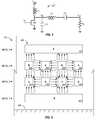
- FIG. 3is a schematic diagram of a power amplifier formed on an integrated circuit that may utilize the capacitor structures of the present invention.
- FIG. 4is sectional view of an example of a capacitor structure of the present invention.
- FIGS. 5-13show additional examples of shielded capacitors of the present invention.
- the present inventionsolves the problems discussed above by providing shielding to a capacitor structure formed in a semiconductor device.
- the present inventionprovides a capacitor formed in an integrated circuit with one or more layers of conductive strips (i.e., capacitor fingers) connected to one of two nodes of the capacitor.
- One or more shieldsare disposed adjacent to the layers of conductive strips and are also connected to one of the nodes. The shields confine the electric fields between the nodes between the limits of the shields.
- the present inventionmay include numerous variations within the spirit and scope of the invention.
- FIG. 3is a schematic diagram of a power amplifier 302 formed on an integrated circuit for use with a wireless transmission system such as a wireless telephone or other device.
- the power amplifier 302includes capacitors C 1 and C 2 , which may be implemented using the shielded capacitor structure of the present invention.
- the inventionmay be applied to GSM, CDMA, PCS, DCS, etc., or other wireless systems.
- the present inventionmay be used in any application where a shielded capacitor structure is desirable.
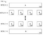
- FIG. 4is sectional view of an example of a capacitor structure of the present invention.
- FIG. 4shows a capacitor 400 formed on a silicon substrate 402 as part of an integrated circuit 401 (other components of the integrated circuit 401 are not shown). Note that the structure of the integrated circuit 401 extends beyond what is shown in FIG. 4 .
- the structure of the integrated circuit 401may extend past the capacitor 400 , as shown in FIG. 4 .
- the integrated circuit 401may also include components placed above or below the capacitor 400 . Similarly, this also applies to the embodiments shown in FIGS. 5-13 (described below), even though FIGS. 5-13 only show the capacitors.
- the capacitor 400is built using four layers of metal, designated as METAL 1 , METAL 2 , METAL 3 , and METAL 4 .
- METAL 1Formed in the METAL 2 layer is a first row of conductive strips.
- a first set of conductive strips 404is connected to node A of the capacitor.
- a second set of conductive strips 406is connected to node B of the capacitor.
- the conductive strips 404 and 406alternate, although other configurations may also be used.
- a second row of conductive stripsis formed in the METAL 3 layer.
- the second row of conductive stripsalso has first and second sets of conductive strips 404 and 406 connected to nodes A and B of the capacitor.
- FIG. 1Formed in the METAL 2 layer is a first row of conductive strips.
- a first set of conductive strips 404is connected to node A of the capacitor.
- a second set of conductive strips 406is connected to node B of the capacitor.
- a second row of conductive stripsis formed in the
- FIG. 4also shows a first shield 408 formed in the METAL 4 layer above the conductive strips.
- the shield 408is formed by a solid conductive plate and is connected to node A of the capacitor.
- a second shield 410is formed in the METAL 1 layer below the conductive strips.
- the shield 410is formed by a solid conductive plate and is connected to node B of the capacitor.
- a dielectric material, or insulating layers,surrounds and separates the various metal layers.
- FIG. 4also illustrates the electric fields present in the capacitor 400 .
- the shields 408 and 410confine the electric fields from node A to node B (as illustrated by the arrows) within the limits of the shields 408 and 410 .
- One advantage of the capacitor structure shown in FIG. 4is that the capacitance value of the capacitor 400 can be more accurately predicted because it involves only the metal conductors and the dielectric insulator between them. Also, the electric field from nodes A to B does not pass through materials such as the Silicon substrate 402 below the first metal layer or components above the top metal layer.
- the capacitor structure of FIG. 4has shunt capacitance from the shield 410 to any conductors below the first metal layer and from the shield 408 to any conductors above the topmost metal layer. However, this shunt capacitance does not affect value of the capacitance between nodes A and B and may not need to be predicted as accurately.
- shunt capacitance to the shield 408is very small but that to the shield 410 from the underlying Silicon substrate 402 is fairly large. So, this structure is useful in cases where shunt capacitance from node B is less critical than shunt capacitance from node A.
- a shielded capacitor structure of the present inventioncan take on many configurations in addition to the example shown in FIG. 4 .
- FIGS. 5-13show additional examples of shielded capacitors of the present invention. Note that, in addition to the examples given, other embodiments are also possible. In addition, various combinations of configurations are also possible.
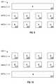
- FIG. 5shows a capacitor 500 , which is similar to the capacitor 400 shown in FIG. 4 , except that the conductive strips 504 and 506 are arranged differently.
- FIG. 5includes a first shield 508 formed in the METAL 4 layer and a second shield 510 formed in the METAL 1 layer.
- the conductive strips 504 connected to node A in the METAL 3 layerare positioned above the conductive strips 504 connected to node A in the METAL 2 layer.
- the conductive strips 506 connected to node B in the METAL 3 layerare positioned above the conductive strips 506 connected to node B in the METAL 2 layer.
- FIG. 6shows an example of a capacitor 600 where the conductive strips 604 and 606 are not all the same size and not all aligned.
- the capacitor 600may be used, for example, when the process-specified minimum widths of conductors in one metal layer (e.g., METAL 2 ) is different from that in another metal layer (e.g., METAL 3 ). Conductive strips in various layers can therefore have the same or different widths and spacing.
- FIG. 7shows an example of a capacitor 700 where the shields 708 and 710 are comprised of conductive strips 704 and 706 rather than a continuous metal plate.
- the shields 708 and 710are illustrated by a dashed box around the conductive strips formed in the METAL 1 and METAL 4 layers.
- FIG. 8shows an example of a capacitor 800 that, in addition to the top shield 808 and the bottom shield 810 , has a side shield 812 .
- the side shield 812is formed by conductive strips 804 formed on the METAL 1 , 2 , and 3 layers and connected to node A.
- the conductive strips 804 of the side shield 812are connected to each other, and to the top shield 808 , by vias 814 .
- the side shield 812could also be made from conductive strips 806 connected to node B.
- a side shieldcould be formed on both sides of the capacitor 800 , or used without top and/or bottom shields.
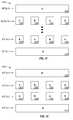
- FIG. 9shows an example of a capacitor 900 similar to the capacitor 400 shown in FIG. 4 with only a top shield 908 .
- FIG. 10shows a capacitor 1000 with only a bottom shield 1010 .
- only one shieldmay be necessary.
- a structurecan be used that includes only the lower shield plate 1010 ( FIG. 10 ).
- a structurecan be used that includes only the upper shield plate 908 ( FIG. 9 ).
- a capacitor structure of the present inventionmay be formed using any number of layers of conductive strips.
- FIG. 11shows an example of a capacitor 1100 formed on N metal layers and having N ⁇ 2 layers of conductive strips 1104 and 1106 .
- FIG. 12shows an example of a capacitor 1200 where the top shield 1208 and bottom shield 1210 are connected to the same node (node B in this example).
- FIG. 13shows an example of a capacitor 1300 where the top and bottom shields 1308 and 1310 are connected to a third node, shown in this example as reference voltage (e.g., ground) rather than to nodes A or B.
- reference voltagee.g., ground
Landscapes
- Engineering & Computer Science (AREA)
- Power Engineering (AREA)
- Physics & Mathematics (AREA)
- Condensed Matter Physics & Semiconductors (AREA)
- General Physics & Mathematics (AREA)
- Computer Hardware Design (AREA)
- Microelectronics & Electronic Packaging (AREA)
- Semiconductor Integrated Circuits (AREA)
Abstract
Description
Claims (11)
Priority Applications (1)
| Application Number | Priority Date | Filing Date | Title |
|---|---|---|---|
| US11/931,083US7754606B2 (en) | 2002-03-11 | 2007-10-31 | Shielded capacitor structure |
Applications Claiming Priority (4)
| Application Number | Priority Date | Filing Date | Title |
|---|---|---|---|
| US10/094,859US6737698B1 (en) | 2002-03-11 | 2002-03-11 | Shielded capacitor structure |
| US10/814,616US6969680B2 (en) | 2002-03-11 | 2004-03-31 | Method for making shielded capacitor structure |
| US11/291,074US7714371B2 (en) | 2002-03-11 | 2005-11-29 | Shielded capacitor structure |
| US11/931,083US7754606B2 (en) | 2002-03-11 | 2007-10-31 | Shielded capacitor structure |
Related Parent Applications (1)
| Application Number | Title | Priority Date | Filing Date |
|---|---|---|---|
| US11/291,074ContinuationUS7714371B2 (en) | 2002-03-11 | 2005-11-29 | Shielded capacitor structure |
Publications (2)
| Publication Number | Publication Date |
|---|---|
| US20080274612A1 US20080274612A1 (en) | 2008-11-06 |
| US7754606B2true US7754606B2 (en) | 2010-07-13 |
Family
ID=32296432
Family Applications (4)
| Application Number | Title | Priority Date | Filing Date |
|---|---|---|---|
| US10/094,859Expired - Fee RelatedUS6737698B1 (en) | 2002-03-11 | 2002-03-11 | Shielded capacitor structure |
| US10/814,616Expired - LifetimeUS6969680B2 (en) | 2002-03-11 | 2004-03-31 | Method for making shielded capacitor structure |
| US11/291,074Expired - Fee RelatedUS7714371B2 (en) | 2002-03-11 | 2005-11-29 | Shielded capacitor structure |
| US11/931,083Expired - Fee RelatedUS7754606B2 (en) | 2002-03-11 | 2007-10-31 | Shielded capacitor structure |
Family Applications Before (3)
| Application Number | Title | Priority Date | Filing Date |
|---|---|---|---|
| US10/094,859Expired - Fee RelatedUS6737698B1 (en) | 2002-03-11 | 2002-03-11 | Shielded capacitor structure |
| US10/814,616Expired - LifetimeUS6969680B2 (en) | 2002-03-11 | 2004-03-31 | Method for making shielded capacitor structure |
| US11/291,074Expired - Fee RelatedUS7714371B2 (en) | 2002-03-11 | 2005-11-29 | Shielded capacitor structure |
Country Status (1)
| Country | Link |
|---|---|
| US (4) | US6737698B1 (en) |
Cited By (5)
| Publication number | Priority date | Publication date | Assignee | Title |
|---|---|---|---|---|
| US20090096533A1 (en)* | 2007-10-16 | 2009-04-16 | Paul Susanne A | Adaptively tuned rf power amplifier |
| US20100140738A1 (en)* | 2007-04-12 | 2010-06-10 | Stats Chippac, Ltd. | Semiconductor Device and Method of Forming Compact Coils for High Performance Filter |
| US10102977B2 (en) | 2014-06-10 | 2018-10-16 | Smart Hybrid Systems Incorporated | High energy density capacitor with micrometer structures and nanometer components |
| US10312026B2 (en) | 2015-06-09 | 2019-06-04 | Smart Hybird Systems Incorporated | High energy density capacitor with high aspect micrometer structures and a giant colossal dielectric material |
| WO2023219774A1 (en)* | 2022-05-10 | 2023-11-16 | Qualcomm Incorporated | Matching unit capacitor with multiple metal layers |
Families Citing this family (59)
| Publication number | Priority date | Publication date | Assignee | Title |
|---|---|---|---|---|
| US20020040991A1 (en)* | 2000-08-18 | 2002-04-11 | Sherif Embabi | Variable capacitor for tuned circuits |
| US6737698B1 (en)* | 2002-03-11 | 2004-05-18 | Silicon Laboratories, Inc. | Shielded capacitor structure |
| US6963122B1 (en)* | 2003-02-21 | 2005-11-08 | Barcelona Design, Inc. | Capacitor structure and automated design flow for incorporating same |
| US7259956B2 (en)* | 2003-12-19 | 2007-08-21 | Broadcom Corporation | Scalable integrated circuit high density capacitors |
| EP1704583A1 (en)* | 2003-12-23 | 2006-09-27 | Telefonaktiebolaget LM Ericsson (publ) | Capacitor |
| US6903918B1 (en)* | 2004-04-20 | 2005-06-07 | Texas Instruments Incorporated | Shielded planar capacitor |
| US7154734B2 (en)* | 2004-09-20 | 2006-12-26 | Lsi Logic Corporation | Fully shielded capacitor cell structure |
| JP4583132B2 (en)* | 2004-10-08 | 2010-11-17 | 三洋電機株式会社 | Solid electrolytic capacitor |
| BRPI0516390A (en)* | 2004-10-22 | 2008-09-02 | Dow Global Technologies Inc | method for producing a shaped composite article, shaped plastic article, article and article use |
| CN1953181B (en)* | 2005-10-21 | 2010-10-13 | 松下电器产业株式会社 | Analog-digital converter |
| US8076752B2 (en) | 2006-03-20 | 2011-12-13 | Standard Microsystems Corporation | Fringe capacitor using bootstrapped non-metal layer |
| TW200807729A (en)* | 2006-06-02 | 2008-02-01 | Kenet Inc | Improved metal-insulator-metal capacitors |
| US7403147B2 (en)* | 2006-11-29 | 2008-07-22 | Sitime Corporation | Precision capacitor array |
| US20080128857A1 (en)* | 2006-12-05 | 2008-06-05 | Integrated Device Technology, Inc. | Multi-Finger Capacitor |
| TWI326495B (en)* | 2006-12-29 | 2010-06-21 | Ind Tech Res Inst | Common centroid symmetry capacitor |
| TWI320964B (en)* | 2006-12-29 | 2010-02-21 | Ind Tech Res Inst | Face center cube capacitor and manufacture method thereof |
| JP2008235498A (en)* | 2007-03-20 | 2008-10-02 | Renesas Technology Corp | Semiconductor device |
| US7838919B2 (en)* | 2007-03-29 | 2010-11-23 | Panasonic Corporation | Capacitor structure |
| US20090015983A1 (en)* | 2007-07-12 | 2009-01-15 | Western Lights Semiconductor Corp. | Parallel plate capacitor |
| US20090141423A1 (en)* | 2007-07-12 | 2009-06-04 | James Chyi Lai | Parallel plate magnetic capacitor and electric energy storage device |
| GB2466840B (en)* | 2009-01-12 | 2011-02-23 | Northern Lights Semiconductor | A parallel plate magnetic capacitor and electric energy storage device |
| US20090160019A1 (en)* | 2007-12-20 | 2009-06-25 | Mediatek Inc. | Semiconductor capacitor |
| US20100038752A1 (en)* | 2008-08-15 | 2010-02-18 | Chartered Semiconductor Manufacturing, Ltd. | Modular & scalable intra-metal capacitors |
| US8716778B2 (en)* | 2008-11-17 | 2014-05-06 | Altera Corporation | Metal-insulator-metal capacitors |
| US7956438B2 (en)* | 2008-11-21 | 2011-06-07 | Xilinx, Inc. | Integrated capacitor with interlinked lateral fins |
| JP5540006B2 (en)* | 2008-11-21 | 2014-07-02 | ザイリンクス インコーポレイテッド | Shielding for integrated capacitors |
| US7994610B1 (en) | 2008-11-21 | 2011-08-09 | Xilinx, Inc. | Integrated capacitor with tartan cross section |
| US7994609B2 (en)* | 2008-11-21 | 2011-08-09 | Xilinx, Inc. | Shielding for integrated capacitors |
| US8207592B2 (en)* | 2008-11-21 | 2012-06-26 | Xilinx, Inc. | Integrated capacitor with array of crosses |
| US8362589B2 (en)* | 2008-11-21 | 2013-01-29 | Xilinx, Inc. | Integrated capacitor with cabled plates |
| US7944732B2 (en)* | 2008-11-21 | 2011-05-17 | Xilinx, Inc. | Integrated capacitor with alternating layered segments |
| TW201110167A (en)* | 2009-09-04 | 2011-03-16 | Novatek Microelectronics Corp | Metal-oxide-metal capacitor having low parasitic capacitor |
| US10283443B2 (en) | 2009-11-10 | 2019-05-07 | Taiwan Semiconductor Manufacturing Co., Ltd. | Chip package having integrated capacitor |
| US9941195B2 (en) | 2009-11-10 | 2018-04-10 | Taiwan Semiconductor Manufacturing Co., Ltd. | Vertical metal insulator metal capacitor |
| US8810002B2 (en)* | 2009-11-10 | 2014-08-19 | Taiwan Semiconductor Manufacturing Company, Ltd. | Vertical metal insulator metal capacitor |
| US9343237B2 (en) | 2009-11-10 | 2016-05-17 | Taiwan Semiconductor Manufacturing Company, Ltd. | Vertical metal insulator metal capacitor |
| JP5732742B2 (en) | 2010-04-16 | 2015-06-10 | 富士通セミコンダクター株式会社 | Semiconductor integrated circuit device and manufacturing method thereof |
| US8199457B1 (en)* | 2010-08-16 | 2012-06-12 | Rockwell Collins, Inc. | Microfabricated RF capacitor |
| IT1403475B1 (en)* | 2010-12-20 | 2013-10-17 | St Microelectronics Srl | CONNECTION STRUCTURE FOR AN INTEGRATED CIRCUIT WITH CAPACITIVE FUNCTION |
| US8653844B2 (en) | 2011-03-07 | 2014-02-18 | Xilinx, Inc. | Calibrating device performance within an integrated circuit |
| JP5404678B2 (en) | 2011-03-10 | 2014-02-05 | 株式会社東芝 | Power control device |
| US8941974B2 (en) | 2011-09-09 | 2015-01-27 | Xilinx, Inc. | Interdigitated capacitor having digits of varying width |
| US9287209B2 (en)* | 2011-11-04 | 2016-03-15 | Broadcom Corporation | Metal finger capacitor for high-K metal gate processes |
| JP2014120615A (en) | 2012-12-17 | 2014-06-30 | Fujitsu Semiconductor Ltd | Capacity element, capacity array, and a/d converter |
| US9312221B2 (en)* | 2013-06-13 | 2016-04-12 | Taiwan Semiconductor Manufacturing Co., Ltd. | Variable capacitance devices |
| US9054069B2 (en)* | 2013-09-05 | 2015-06-09 | International Business Machines Corporation | Variable capacitance integrated circuit |
| US9270247B2 (en) | 2013-11-27 | 2016-02-23 | Xilinx, Inc. | High quality factor inductive and capacitive circuit structure |
| US9331026B1 (en) | 2014-05-09 | 2016-05-03 | Altera Corporation | Methods and apparatus for fabricating capacitor structures with a terminal shield |
| US9524964B2 (en) | 2014-08-14 | 2016-12-20 | Xilinx, Inc. | Capacitor structure in an integrated circuit |
| US9887257B2 (en) | 2015-12-01 | 2018-02-06 | Altera Corporation | Scalable fixed-footprint capacitor structure |
| JP6384553B2 (en)* | 2017-02-07 | 2018-09-05 | 株式会社ソシオネクスト | Capacitor element, capacitor array, and A / D converter |
| US10978387B2 (en)* | 2017-05-25 | 2021-04-13 | Taiwan Semiconductor Manufacturing Co., Ltd. | Semiconductor device and method for manufacturing the same |
| US10916622B2 (en) | 2017-09-28 | 2021-02-09 | Stmicroelectronics S.R.L. | High-voltage capacitor, system including the capacitor and method for manufacturing the capacitor |
| IT201700108918A1 (en)* | 2017-09-28 | 2019-03-28 | St Microelectronics Srl | CONDENSER FOR HIGH VOLTAGE SHIELDED, SYSTEM INCLUDING THE CONDENSER AND METHOD OF MANUFACTURING THE CONDENSER |
| EP3514828B1 (en)* | 2018-01-19 | 2021-08-25 | Socionext Inc. | Semiconductor integrated circuitry |
| US10686031B2 (en)* | 2018-03-27 | 2020-06-16 | Qualcomm Incorporated | Finger metal-oxide-metal (FMOM) capacitor |
| CN114175292A (en) | 2019-06-28 | 2022-03-11 | 可尔Hw半导体公司 | Capacitor Structure and Chip Antenna |
| EP4007001A1 (en) | 2020-11-30 | 2022-06-01 | NXP USA, Inc. | Integrated capacitors in an integrated circuit |
| US11626366B2 (en)* | 2021-06-22 | 2023-04-11 | Silicon Laboratories Inc. | Shielding using layers with staggered trenches |
Citations (3)
| Publication number | Priority date | Publication date | Assignee | Title |
|---|---|---|---|---|
| US5166687A (en)* | 1991-06-17 | 1992-11-24 | Texas Instruments Incorporated | Apparatus and method for enhancing capacitance matching in a multi-stage weighted capacitor a/d converter with conductive shields |
| US5583359A (en)* | 1995-03-03 | 1996-12-10 | Northern Telecom Limited | Capacitor structure for an integrated circuit |
| US6097581A (en)* | 1997-04-08 | 2000-08-01 | X2Y Attenuators, Llc | Paired multi-layered dielectric independent passive component architecture resulting in differential and common mode filtering with surge protection in one integrated package |
Family Cites Families (20)
| Publication number | Priority date | Publication date | Assignee | Title |
|---|---|---|---|---|
| US3593319A (en) | 1968-12-23 | 1971-07-13 | Gen Electric | Card-changeable capacitor read-only memory |
| US4470096A (en)* | 1982-06-18 | 1984-09-04 | Motorola Inc. | Multilayer, fully-trimmable, film-type capacitor and method of adjustment |
| US4758922A (en)* | 1986-11-14 | 1988-07-19 | Matsushita Electric Industrial Co., Ltd. | High frequency circuit having a microstrip resonance element |
| US4870541A (en)* | 1987-12-16 | 1989-09-26 | Ford Micro Electronics | Shielded bar-cap |
| JP2504606B2 (en) | 1990-05-18 | 1996-06-05 | 株式会社東芝 | Semiconductor memory device and manufacturing method thereof |
| US5220483A (en)* | 1992-01-16 | 1993-06-15 | Crystal Semiconductor | Tri-level capacitor structure in switched-capacitor filter |
| US5635669A (en)* | 1992-07-27 | 1997-06-03 | Murata Manufacturing Co., Ltd. | Multilayer electronic component |
| US5208725A (en) | 1992-08-19 | 1993-05-04 | Akcasu Osman E | High capacitance structure in a semiconductor device |
| JP2809122B2 (en)* | 1994-12-26 | 1998-10-08 | 日本電気株式会社 | Wiring structure of semiconductor integrated circuit and method of manufacturing the same |
| US5552563A (en)* | 1995-03-17 | 1996-09-03 | Sharp Microelectronics Technology, Inc. | Shielded low noise multi-lead contact |
| US5939766A (en) | 1996-07-24 | 1999-08-17 | Advanced Micro Devices, Inc. | High quality capacitor for sub-micrometer integrated circuits |
| US5789807A (en) | 1996-10-15 | 1998-08-04 | International Business Machines Corporation | On-chip power distribution for improved decoupling |
| US6198123B1 (en)* | 1997-08-29 | 2001-03-06 | Cardiac Pacemakers, Inc. | Shielded integrated circuit capacitor connected to a lateral transistor |
| US6066537A (en)* | 1998-02-02 | 2000-05-23 | Tritech Microelectronics, Ltd. | Method for fabricating a shielded multilevel integrated circuit capacitor |
| US6191666B1 (en)* | 1999-03-25 | 2001-02-20 | Industrial Technology Research Institute | Miniaturized multi-layer ceramic lowpass filter |
| US6597259B1 (en)* | 2000-01-11 | 2003-07-22 | James Michael Peters | Selective laminated filter structures and antenna duplexer using same |
| US6410954B1 (en)* | 2000-04-10 | 2002-06-25 | Koninklijke Philips Electronics N.V. | Multilayered capacitor structure with alternately connected concentric lines for deep sub-micron CMOS |
| US6625006B1 (en)* | 2000-09-05 | 2003-09-23 | Marvell International, Ltd. | Fringing capacitor structure |
| US6563191B1 (en)* | 2000-10-16 | 2003-05-13 | Agilent Technologies, Inc. | Interdigitated capacitor with dielectric overlay |
| US6737698B1 (en)* | 2002-03-11 | 2004-05-18 | Silicon Laboratories, Inc. | Shielded capacitor structure |
- 2002
- 2002-03-11USUS10/094,859patent/US6737698B1/ennot_activeExpired - Fee Related
- 2004
- 2004-03-31USUS10/814,616patent/US6969680B2/ennot_activeExpired - Lifetime
- 2005
- 2005-11-29USUS11/291,074patent/US7714371B2/ennot_activeExpired - Fee Related
- 2007
- 2007-10-31USUS11/931,083patent/US7754606B2/ennot_activeExpired - Fee Related
Patent Citations (3)
| Publication number | Priority date | Publication date | Assignee | Title |
|---|---|---|---|---|
| US5166687A (en)* | 1991-06-17 | 1992-11-24 | Texas Instruments Incorporated | Apparatus and method for enhancing capacitance matching in a multi-stage weighted capacitor a/d converter with conductive shields |
| US5583359A (en)* | 1995-03-03 | 1996-12-10 | Northern Telecom Limited | Capacitor structure for an integrated circuit |
| US6097581A (en)* | 1997-04-08 | 2000-08-01 | X2Y Attenuators, Llc | Paired multi-layered dielectric independent passive component architecture resulting in differential and common mode filtering with surge protection in one integrated package |
Cited By (9)
| Publication number | Priority date | Publication date | Assignee | Title |
|---|---|---|---|---|
| US20100140738A1 (en)* | 2007-04-12 | 2010-06-10 | Stats Chippac, Ltd. | Semiconductor Device and Method of Forming Compact Coils for High Performance Filter |
| US8111112B2 (en) | 2007-04-12 | 2012-02-07 | Stats Chippac, Ltd. | Semiconductor device and method of forming compact coils for high performance filter |
| US20090096533A1 (en)* | 2007-10-16 | 2009-04-16 | Paul Susanne A | Adaptively tuned rf power amplifier |
| US7911277B2 (en) | 2007-10-16 | 2011-03-22 | Black Sand Technologies, Inc. | Adaptively tuned RF power amplifier |
| US10102977B2 (en) | 2014-06-10 | 2018-10-16 | Smart Hybrid Systems Incorporated | High energy density capacitor with micrometer structures and nanometer components |
| US11462362B2 (en) | 2014-06-10 | 2022-10-04 | Smart Hybrid Systems Incorporated | High energy density capacitor with micrometer structures and nanometer components |
| US10312026B2 (en) | 2015-06-09 | 2019-06-04 | Smart Hybird Systems Incorporated | High energy density capacitor with high aspect micrometer structures and a giant colossal dielectric material |
| US10903014B2 (en) | 2015-06-09 | 2021-01-26 | Smart Hybird Systems Incorporated | High energy density capacitor with high aspect micrometer structures and a giant colossal dielectric material |
| WO2023219774A1 (en)* | 2022-05-10 | 2023-11-16 | Qualcomm Incorporated | Matching unit capacitor with multiple metal layers |
Also Published As
| Publication number | Publication date |
|---|---|
| US20050030699A1 (en) | 2005-02-10 |
| US6737698B1 (en) | 2004-05-18 |
| US20080274612A1 (en) | 2008-11-06 |
| US20070004198A1 (en) | 2007-01-04 |
| US7714371B2 (en) | 2010-05-11 |
| US6969680B2 (en) | 2005-11-29 |
Similar Documents
| Publication | Publication Date | Title |
|---|---|---|
| US7754606B2 (en) | Shielded capacitor structure | |
| US7663207B2 (en) | Semiconductor device | |
| US7578858B1 (en) | Making capacitor structure in a semiconductor device | |
| US6743671B2 (en) | Metal-on-metal capacitor with conductive plate for preventing parasitic capacitance and method of making the same | |
| US8716778B2 (en) | Metal-insulator-metal capacitors | |
| US5978206A (en) | Stacked-fringe integrated circuit capacitors | |
| US7154734B2 (en) | Fully shielded capacitor cell structure | |
| US6411494B1 (en) | Distributed capacitor | |
| TWI697921B (en) | Capacitor | |
| US6597562B1 (en) | Electrically polar integrated capacitor and method of making same | |
| KR20110098915A (en) | Integrated capacitors with interdigitated transverse fins | |
| US7557426B2 (en) | Integrated capacitor structure | |
| KR20110102346A (en) | Integrated Capacitors with Grid Plates | |
| KR20010079632A (en) | Method for implementing resistance, capacitance and/or inductance in an integrated circuit | |
| CA2550882A1 (en) | Capacitor | |
| US6833781B1 (en) | High Q inductor in multi-level interconnect | |
| JP3781178B2 (en) | Multi-layer wiring structure of high-frequency semiconductor device | |
| US6600209B1 (en) | Mesh capacitor structure in an integrated circuit | |
| US20100067169A1 (en) | Capacitor structure | |
| KR101037009B1 (en) | Capacitor structure | |
| US6812544B2 (en) | Integrated circuit having oversized components | |
| US11837597B2 (en) | Semiconductor capacitor array layout with dummy capacitor structure | |
| US20060270210A1 (en) | Waveguide integrated circuit | |
| JPS62259500A (en) | Circuit board | |
| KR100415547B1 (en) | High-Q poly-to-poly capacitor structure for RF ICs |
Legal Events
| Date | Code | Title | Description |
|---|---|---|---|
| AS | Assignment | Owner name:BLACK SAND TECHNOLOGIES, INC., TEXAS Free format text:ASSIGNMENT OF ASSIGNORS INTEREST;ASSIGNOR:SILICON LABORATORIES INC.;REEL/FRAME:021243/0389 Effective date:20080417 Owner name:BLACK SAND TECHNOLOGIES, INC.,TEXAS Free format text:ASSIGNMENT OF ASSIGNORS INTEREST;ASSIGNOR:SILICON LABORATORIES INC.;REEL/FRAME:021243/0389 Effective date:20080417 | |
| AS | Assignment | Owner name:COMERICA BANK, TEXAS Free format text:SECURITY AGREEMENT;ASSIGNOR:BLACK SAND TECHNOLOGIES, INC.;REEL/FRAME:022343/0475 Effective date:20071115 Owner name:COMERICA BANK,TEXAS Free format text:SECURITY AGREEMENT;ASSIGNOR:BLACK SAND TECHNOLOGIES, INC.;REEL/FRAME:022343/0475 Effective date:20071115 | |
| STCF | Information on status: patent grant | Free format text:PATENTED CASE | |
| FEPP | Fee payment procedure | Free format text:PAYOR NUMBER ASSIGNED (ORIGINAL EVENT CODE: ASPN); ENTITY STATUS OF PATENT OWNER: LARGE ENTITY | |
| REMI | Maintenance fee reminder mailed | ||
| FPAY | Fee payment | Year of fee payment:4 | |
| SULP | Surcharge for late payment | ||
| AS | Assignment | Owner name:SILICON LABORATORIES, INC., TEXAS Free format text:ASSIGNMENT OF ASSIGNORS INTEREST;ASSIGNORS:PAUL, SUSANNE A.;DUPUIS, TIMOTHY J.;NIKNEJAD, ALI M.;SIGNING DATES FROM 20020311 TO 20020319;REEL/FRAME:032913/0376 | |
| AS | Assignment | Owner name:BLACK SAND TECHNOLOGIES, INC., CALIFORNIA Free format text:MERGER;ASSIGNOR:WAVEFORM ACQUISITION CORPORATION;REEL/FRAME:033247/0787 Effective date:20140618 | |
| AS | Assignment | Owner name:BLACK SAND TECHNOLOGIES, INC., TEXAS Free format text:RELEASE OF SECURITY INTEREST;ASSIGNOR:COMERICA BANK;REEL/FRAME:033258/0225 Effective date:20140627 | |
| AS | Assignment | Owner name:BLACK SAND TECHNOLOGIES, INC., TEXAS Free format text:ASSIGNMENT OF ASSIGNORS INTEREST;ASSIGNOR:SILICON LABORATORIES INC.;REEL/FRAME:033500/0122 Effective date:20140612 | |
| AS | Assignment | Owner name:BLACK SAND TECHNOLOGIES INC., CALIFORNIA Free format text:RELEASE OF SECURITY INTEREST;ASSIGNOR:SILICON LABORATORIES INC.;REEL/FRAME:033729/0183 Effective date:20140610 | |
| AS | Assignment | Owner name:QUALCOMM INCORPORATED, CALIFORNIA Free format text:ASSIGNMENT OF ASSIGNORS INTEREST;ASSIGNOR:BLACK SAND TECHNOLOGIES, INC.;REEL/FRAME:034077/0072 Effective date:20141024 | |
| MAFP | Maintenance fee payment | Free format text:PAYMENT OF MAINTENANCE FEE, 8TH YEAR, LARGE ENTITY (ORIGINAL EVENT CODE: M1552) Year of fee payment:8 | |
| FEPP | Fee payment procedure | Free format text:MAINTENANCE FEE REMINDER MAILED (ORIGINAL EVENT CODE: REM.); ENTITY STATUS OF PATENT OWNER: LARGE ENTITY | |
| LAPS | Lapse for failure to pay maintenance fees | Free format text:PATENT EXPIRED FOR FAILURE TO PAY MAINTENANCE FEES (ORIGINAL EVENT CODE: EXP.); ENTITY STATUS OF PATENT OWNER: LARGE ENTITY | |
| STCH | Information on status: patent discontinuation | Free format text:PATENT EXPIRED DUE TO NONPAYMENT OF MAINTENANCE FEES UNDER 37 CFR 1.362 | |
| FP | Lapsed due to failure to pay maintenance fee | Effective date:20220713 |