US7751272B2 - Semiconductor device and method for selection and de-selection of memory devices interconnected in series - Google Patents
Semiconductor device and method for selection and de-selection of memory devices interconnected in seriesDownload PDFInfo
- Publication number
- US7751272B2 US7751272B2US12/025,866US2586608AUS7751272B2US 7751272 B2US7751272 B2US 7751272B2US 2586608 AUS2586608 AUS 2586608AUS 7751272 B2US7751272 B2US 7751272B2
- Authority
- US
- United States
- Prior art keywords
- memory device
- command
- signal
- input
- match
- Prior art date
- Legal status (The legal status is an assumption and is not a legal conclusion. Google has not performed a legal analysis and makes no representation as to the accuracy of the status listed.)
- Expired - Fee Related, expires
Links
Images


Classifications
- G—PHYSICS
- G11—INFORMATION STORAGE
- G11C—STATIC STORES
- G11C19/00—Digital stores in which the information is moved stepwise, e.g. shift registers
- G—PHYSICS
- G11—INFORMATION STORAGE
- G11C—STATIC STORES
- G11C5/00—Details of stores covered by group G11C11/00
- G11C5/14—Power supply arrangements, e.g. power down, chip selection or deselection, layout of wirings or power grids, or multiple supply levels
- G—PHYSICS
- G11—INFORMATION STORAGE
- G11C—STATIC STORES
- G11C7/00—Arrangements for writing information into, or reading information out from, a digital store
- G11C7/22—Read-write [R-W] timing or clocking circuits; Read-write [R-W] control signal generators or management
- G—PHYSICS
- G11—INFORMATION STORAGE
- G11C—STATIC STORES
- G11C8/00—Arrangements for selecting an address in a digital store
- G11C8/12—Group selection circuits, e.g. for memory block selection, chip selection, array selection
- G—PHYSICS
- G11—INFORMATION STORAGE
- G11C—STATIC STORES
- G11C8/00—Arrangements for selecting an address in a digital store
- G11C8/18—Address timing or clocking circuits; Address control signal generation or management, e.g. for row address strobe [RAS] or column address strobe [CAS] signals
Definitions
- the present inventionrelates generally to semiconductor devices. More particularly, the present invention relates to a system having an arrangement having a plurality of semiconductor devices.
- a memory devicefor use in an arrangement of memory devices interconnected in series.
- the memory devicecomprises: a first input for receiving a command input signal containing a command and an identification number; a second input for receiving a first strobe signal indicating the start of command; and logic circuitry.
- the logic circuitryis configured to: de-select the memory device in response to the first strobe signal to place the memory device in a de-selected state; determine whether the identification number of the command matches a device address associated with the memory device; and in response to a determination result, place the memory device in a selected state.
- the logic circuitrymay be further configured to: refrain from forwarding the command input signal and the first strobe signal while the memory device is in the selected state; and transfer the command input signal and the first strobe signal while the memory device is in the de-selected state.
- the memory devicestays in the de-selected state and the entire command is forwarded. If there is a match, only a truncated part of the command is forwarded before the memory device is placed in the selected state.
- the memory devicemay further include a third input for receiving clock input.
- the command input signalis forwarded with a delay related to clock cycle latency while the memory device is in the de-selected state.
- the command strobe signalmay be forwarded with a delay related to clock cycle latency while the memory device is in the de-selected state.
- the memory devicemay further include a fourth input for receiving a second strobe signal containing data enabling data output from the memory device in the selected state.
- the logic circuitrymay forward the second strobe signal with a delay related to a latency that is substantially equal to the latency of a delayed version of the command strobe signal.
- a method in a memory device in an arrangement of memory devices interconnected in seriescomprises: receiving a command input signal containing a command; receiving a command strobe signal containing a command strobe indicating the start of command; forwarding the command input signal and the command strobe signal with delays while the memory device is in a de-selected state; de-selecting the memory device when the command strobe signal is received at the start of the command to place the memory device in the de-selected state; determining whether an identification number of the command matches a device address associated with the memory device; and placing the memory device in a selected state if the identification number of the command matches the device address associated with the memory device.
- the methodmay further comprise refraining from forwarding the command input signal and the command strobe signal with delays while the memory device is in the selected state.
- a systemcomprising: a memory controller; and a plurality of memory devices interconnected in series, each of the devices including: a first input for receiving a command input signal containing a command and an identification number; a second input for receiving a first strobe signal indicating the start of command; and logic circuitry.
- the logic circuitryis configured to: de-select the memory device in response to the first strobe signal to place the memory device in a de-selected state; determine whether the identification number of the command matches a device address associated with the memory device; and in response to a determination result, place the memory device in a selected state.
- a systemincludes a plurality of memory devices connected in-series and a memory controller.
- a memory devicereceives a command strobe signal indicating the start of an incoming command
- the memory deviceis placed in a de-selected state and an ID number of the command is compared to the device address of the memory device.
- delayed versions of the command strobe signal and the commandare forwarded. If the ID number matches the device address, the memory device is placed in a selected state. In the selected state, the memory device refrains from forwarding the delayed versions of the command strobe signal and the command. If there is a match, a truncated part of the command is forwarded before the memory device is placed in the selected state.
- FIG. 1is a block diagram of a plurality of memory devices interconnected in series, to which embodiments of the present invention are applicable;
- FIG. 2is a schematic of example command formats for the memory devices interconnected in series
- FIG. 3Ais a block diagram of a system having a memory controller and a plurality of memory devices interconnected in series, to which embodiments of the present invention are applicable;
- FIG. 3Bis a block diagram showing part of the series-connected memory devices shown in FIG. 3A ;
- FIG. 4Ais a schematic of example circuitry of a memory device shown in FIG. 3A ;
- FIG. 4Bis a schematic of an example of forwarding logic circuitry and an internal clock generator of the memory device shown in FIG. 4A ;
- FIG. 4Cis a schematic of an example of a control logic and memory circuitry of the memory device shown in FIG. 4A ;
- FIG. 5is a signaling diagram for example signals in the circuitry shown in FIGS. 4B and 4C ;
- FIGS. 6A and 6Bare signaling diagrams of example signals in the circuitry shown in FIGS. 4B and 4C ;
- FIG. 7is a signaling diagram of example signals in the circuitry shown in FIGS. 4B and 4C ;
- FIG. 8is a circuit diagram of another example of the comparator shown in FIG. 4B ;
- FIG. 9is a circuit diagram of an example of exclusive OR (EXOR) circuitry of the comparator shown in FIG. 8 .
- EXORexclusive OR
- the present inventionrelates generally to a system having an arrangement including a plurality of semiconductor devices.
- the devicesmay operate with different power consumption levels.
- Examples of the semiconductor devicesare processors and memory devices that may operate with different power consumption levels.
- the memory devicesmay be volatile memory devices (e.g., random accesses memories) or non-volatile memory devices (e.g., flash devices).
- Examples described hereincan find application in serial interconnections having a plurality of devices connected in-series. More generally, the embodiments described herein can find application in system architectures employing serial interconnection configurations having a plurality of semiconductor devices connected in-series by serial links or parallel links. Serial interconnection arrangements form a subset of architectures in which devices are connected together in-series with serial or parallel links.
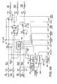
- FIG. 1shows an arrangement of a plurality of memory devices interconnected in series to which embodiments of the present invention are applicable.
- an arrangement 100includes N memory devices 101 - 1 , 101 - 2 , 101 - 3 , - - - , and 101 -N that are series-connected, N being an integer.
- a memory controller(not shown) sends a group of signals of data and information to the memory devices of the arrangement 100 . Data or information to be processed is sent to the first device 101 - 1 and propagated through the devices of the series interconnected arrangement 100 under conditions.
- the output of the last device 101 -Nis open.
- the output of the last device 101 -Nis connected to the memory controller (not shown), so that the memory controller can use the feedback data from the last device 101 -N.
- Each of the memory devices 101 - 1 , 101 - 2 , 101 - 3 , - - - , and 101 -N of the series interconnected arrangement 100has a unique device address (DA) or device identification number (ID).
- the device addresses of the device 101 - 1 , 101 - 2 , 101 - 3 , - - - , and 101 -Nare “0”, “1”, “2”, - - - , and “N ⁇ 1”, respectively.
- the device addresses (DAs)are represented by four bit binary codes ‘0000’, ‘0001’, ‘0010’, - - - , and ‘1110’, respectively.
- Each devicehas its MSB (most significant bit) first and has its LSB (least significant bit) last.
- the DAcan be changed to the LSB first and the MSB last.
- the DAscan be successive numbers from another value (e.g., “1”).
- the DAscan be decremented numbers from a maximum value.
- the memory controllerissues control information including a specific device address and a command.
- the memory device identified by the specific device addressexecutes the command, in accordance with device address matching. Examples of the command are memory accesses and data processes.
- Each commandincludes an ID number (i.e., a device address) and a command OP code (hereinafter simply ‘OP code’), and may also include address information and/or data.
- FIG. 2is a schematic of example command formats for the memory devices interconnected in series.
- a first command format 109 - 1includes an ID number and an OP code. The ID number is used to uniquely identify a selected memory device, while the OP code field contains the OP code to be executed by the selected device. Commands with the first command format 109 - 1 may for example be used for commands containing OP codes for reading a register value.
- a second command format 109 - 2includes an ID number, an OP code and data. Commands with the second command format 109 - 2 may for example be used for commands containing OP codes for writing data to a register.
- a third command format 109 - 3includes an ID number, an OP code, and additional addresses.
- the additional addressesmay for example include row and/or column addresses for addressing a location in memory cells.
- Commands with the third command format 109 - 3may for example be used for commands containing OP codes for reading data from memory cells of a selected memory device.
- a fourth command format 109 - 4includes an ID number, an OP code, additional addresses, and data. Commands with the fourth command format 109 - 4 may for example be used for commands containing OP codes for writing data to the memory cells of a selected memory device. Note that all four example command formats 109 - 1 , 109 - 2 , 109 - 3 , 109 - 4 start with an ID number for addressing purposes.
- commanddoes not merely refer to a command OP code, as a command may include an ID number, an OP code, additional addresses, data, or any other information relating to the control of an arrangement of memory devices interconnected in series.
- FIG. 3Ashows a system having a memory controller and a plurality of memory devices to which embodiments of the present invention are applicable.
- FIG. 3Bshows part of the series-connected memory devices shown in FIG. 3A .
- command input signal SCIi input to a device 131 - ican be transmitted to the next device 131 -( i+ 1).
- a system 110includes a plurality (N) of memory devices interconnected in series, where N is an integer. In the illustrated example, the number of devices N is 15 and thus, memory devices 131 - 1 , 131 - 2 , 131 - 3 , - - - , and 131 - 15 are interconnected in series.
- the system 110also includes a memory controller 120 connected to the first memory device 131 - 1 via a link 121 . Each pair of adjacent memory devices is similarly connected via a link.
- the last (15th) memory device 131 - 15is connected to the memory controller 120 via a link 122 , thereby creating a specific type of series architecture, namely a ring configuration with a feedback path.
- the series architecturewould be a non-feedback configuration.
- the last memory device 131 - 15may be connected to some other component instead of the memory controller 120 . Ring configuration and non-feedback configuration are both examples of architectures featuring devices connected together in series.
- the links interconnecting the memory devices 131 - 1 , 131 - 2 , 131 - 3 , - - - , and 131 - 15are used to transmit commands over a path that traverses the memory devices 131 - 1 , 131 - 2 , 131 - 3 , - - - , and 131 - 15 .
- the first memory device 131 - 1has a command input Dn and a corresponding command output Qn.
- each of the other memory devices 131 - 2 , 131 - 3 , - - - , and 131 - 15has a command input Dn and a corresponding command output Qn.
- the links of the pathform an n-bit wide path.
- the linksare serial links when the path is a single bit wide path (i.e., when n is equal to 1). Otherwise, the links are parallel links (i.e., when n is greater than 1).
- the first memory device 131 - 1has a command strobe input CSI and a corresponding command strobe output CSO.
- each of the other memory devices 131 - 2 , 131 - 3 , - - - , and 131 - 15has a command strobe input CSI and a corresponding command strobe output CSO.
- the command strobe input and outputare for receiving and forwarding a command strobe signal transmitted by the memory controller 120 for enabling command input to the memory devices 131 - 1 , 131 - 2 , 131 - 3 , - - - , and 131 - 15 .
- each of the deviceshas a data strobe input DSI and corresponding data strobe output DSO for transmitting a data strobe signal for enabling output from the memory devices 131 - 1 , 131 - 2 , 131 - 3 , - - - , and 131 - 15 during read operation.
- each devicehas a clock input CLK for receiving a clock signal SCLK.
- the clockis fed to each of the devices in a common source clock fashion.
- a reset signal /RSTis proved to each of the devices by the memory controller 120 . Additional interconnections may be provided for operation, for example, a chip select (not shown).
- memory devices 131 - 1 , 131 - 2 , 131 - 3 , - - - , and 131 - 15are included in the illustrated example, more generally, there may be any appropriate number of memory devices interconnected in series with the memory controller 120 .
- the memory controller 120sends commands over an output communication path established by link 121 and receives responses over an input communication path established by the link 122 for those commands that requisition a response. For each command, the memory controller 120 asserts the command strobe signal SCS 1 for enabling the first device 131 - 1 to receive the command.
- Each of the memory device 131 - 1 , 131 - 2 , 131 - 3 , - - - , and 131 - 15has a unique device address (DA).
- the memory devices 131 - 1 , 131 - 2 , 131 - 3 , - - - , and 131 - 15have device addresses 0000, 0001, 0010, - - - , and 1110, respectively, but more generally the addresses are implementation specific.
- Each command issued from the memory controller 120includes an ID number that matches the device address of a specific memory device (i.e., a selected or designated device). Whenever a memory device receives a command validated by the command strobe signal SCSi input to the command input Dn thereof, it determines whether the ID number (or DA) of the command matches its device address.
- the memory deviceexecutes the OP code identified by the OP code field of the command.
- the command formatis shown in FIG. 2 . Otherwise, the memory device does not execute the OP code identified by the OP code field of the command and merely forwards the command on to the next memory device.
- Each of the memory devices 131 - 1 , 131 - 2 , 131 - 3 , - - - , and 131 - 15includes respective forwarding logic circuitry (not shown), which sets a state of the memory device that controls the forwarding of signals, such as those received on the command strobe input CSI and the command input Dn, to the next memory device, and respective control logic circuitry and memory (not shown), which controls the internal operation of the memory device's handling of commands and memory operations.
- forwarding logic and control logic circuitry and memoryis described below with reference to FIGS. 4A , 4 B and 4 C.
- the second memory device 131 - 2has been previously selected by the memory controller 120 , i.e., the device address of a previous command matched the device address of the second memory device 131 - 2
- the second memory device 131 - 2is first de-selected so that the subsequent command may be passed to the next memory device.
- a selected memory deviceIf a selected memory device is not de-selected when the command strobe signal SCSi is asserted, the selected memory device will not pass the command strobe signal SCSi received at its command strobe input CSI, and the command received on its command input Dn, to the next memory device to which it is interconnected in series.
- Each of the devices 131 - 1 , 131 - 2 , 131 - 3 , - - - , and 131 - 15 shown in FIG. 3Aincludes forwarding logic circuitry, control circuitry and an array of memory cells. A general structure of the forwarding and logic circuitry will be described with reference to FIGS. 4A , 4 B and 4 C.
- FIGS. 4A , 4 B and 4 Cshow example circuitry of one of the memory devices that are interconnected in series, with a memory controller or other memory devices via links as shown in FIG. 1 or 3 A. It is to be understood that the example circuitry shown in FIGS. 4A , 4 B and 4 C is very specific and is provided for example purposes only.
- a representing memory device 131 - iincludes forwarding logic circuitry 165 , control logic and memory circuitry 166 and an internal clock generator 184 .
- the forwarding logic circuitry 165is circuitry for forwarding on inputs to outputs, and includes circuitry for determining whether or not to operate the control logic and memory circuitry 166 , with reduced power consumption.
- the internal clock generator 184produces various clock signals for operating the control logic and memory circuitry 166 .
- the division between the forwarding logic circuitry 165 and the control logic and memory circuitry 166is rather arbitrary.
- the memory device 131 - iincludes four inputs: a command input (Dn) 181 for receiving incoming commands on the command input signal SCIi, a clock input (CLK) 182 for receiving the clock signal SCLK, a command strobe input (CSI) 183 for receiving the command strobe signal SCSi to enable command input, and a data strobe input (DSI) 244 for receiving the data strobe signal SDSi to output data.
- these four inputs 181 , 182 , 183 , 244are inputs to the forwarding logic circuitry 165 .
- the reset signal /RSTis also provided to the forwarding logic circuitry 165 .
- the memory device 131 - ialso includes three outputs: a command output (Qn) 197 for outputting the command input signal SCI(i+1), a command strobe output (CSO) 213 for outputting the command strobe signal SCS(i+1) and a data strobe output (DSO) 226 for outputting the data strobe signal SDS(i+1).
- these three outputs 197 , 213 , 226are outputs of the forwarding logic circuitry 165 .
- the command input signal SCI(i+1), the command strobe signal SCS(i+1) and the data strobe signal SDS(i+1) from the present memory device 131 - iare transmitted to the next memory device 131 -( l +1).
- the forwarding logic circuitry 165provides an ID match signal 198 , an internal clock signal “iSCLK” 204 , and an internal command strobe signal “iSCSi” 205 to the internal clock generator 184 .
- the forwarding logic circuitry 165provides the ID match signal 198 , an internal command input signal “iSCIi” 203 , and an internal data strobe signal “iSDSi” 225 to the control logic and memory circuitry 166 .
- the internal clock generator 184provides a command clock signal 200 , an address clock signal 201 , a data clock signal 202 and an ID clock signal 199 to the control logic and memory circuitry 166 .
- the control logic and memory circuitry 166provides a data output signal 254 to the forwarding logic circuitry 165 .
- FIGS. 4B and 4Cshow detailed examples of very specific implementations of the forwarding logic circuitry 165 and control logic and memory circuitry 166 shown in FIG. 4A , respectively.
- FIGS. 4B and 4Care provided as examples only, and should not be considered to be limiting.
- a command contained in the command input signal SCIiis received over the command input Dn 181 with the command strobe signal SCSi asserted.
- the forwarding logic circuitry 165detects the assertion of the command strobe signal SCSi and de-asserts the ID match signal 198 , effectively placing the memory device 131 - i in a de-selected state.
- the command input signal SCIi and the command strobe signal SCSiare only passed on to the next memory device 131 -( i+ 1) as the command input signal SCI(i+1) and the command strobe signal SCS(i+1) if the present memory device 131 - i is in the de-selected state, i.e., the ID match signal 198 is not asserted. Effectively, de-asserting ID match signal 198 clears any previous selection of the device and allows the command input signal SCIi and the command strobe signal SCSi to be forwarded on to the next device 131 -( i+ 1) via its command output Qn 197 and the command strobe output CSO 213 , respectively.
- the data strobe signal SDSiis passed on to the next memory device 131 -( i+ 1) via the data strobe output DSO 226 , regardless of whether the current memory device is in a selected or de-selected state.
- the forwarding logic circuitry 165After de-asserting ID match signal 198 , which places the memory device 131 - i in the de-selected state, the forwarding logic circuitry 165 compares the device address (DA) of the memory device 131 - i with the device ID that is included at the beginning of the command to determine whether there is a match therebetween. If there is a match between the DA and the ID, then the forwarding logic circuitry 165 asserts the ID match signal 198 in order to indicate an ID match and places the memory device 131 - i in a selected state.
- DAdevice address
- the command input signal SCI(i+1) from the command output Qn 197 and the command strobe signal SCS(i+1) from the command strobe output CSO 213 to the next device 131 -( i+ 1)are truncated, as it has been determined that the command is addressed to the present memory device 131 - i . Therefore, the command and the command strobe do not need to be continued to be forwarded to the next downstream memory device. Otherwise, if there is no match between the DA and the ID, the comparator 190 does not assert the ID match signal 198 , which maintains the memory device in the de-selected state. A delayed version of the command input signal SCIi and a delayed version of the command strobe signal SCSi continue to be forwarded to the next downstream memory device.
- the forwarding logic circuitry 165provides the internal command input signal iSCIi 203 derived from the command input signal SCIi, and the internal data strobe signal iSDSi 225 derived from the data strobe signal SDSi, to the control logic and memory circuitry 166 .
- the forwarding logic circuitry 165also produces the three clock signals: command clock signal 200 , address clock signal 201 and data clock signal 202 , which the control logic and memory circuitry 166 uses to interpret commands included in the internal command input signal iSCIi 203 , to address data and to clock data into the memory block(s) of the memory device, respectively.
- the control logic and memory 166produces its own internal output clock and clocks data out to the forwarding logic circuitry 165 as the data output signal 254 .
- all four input signals theretonamely the command input signal SCIi, the clock signal SCLK, the command strobe signal SCSi and the data strobe signal SDSi are buffered by input buffers 206 , 207 , 208 and 227 , respectively.
- the command input signal SCIiis buffered to produce the internal command signal iSCIi 203 that is passed through a D-type flip-flop (D-FF) 196 onto a multiplexer 195 , which produces an output that is buffered by an output buffer 219 to produce the command input signal SCI(i+1).
- D-FFD-type flip-flop
- the command strobe signal SCSi and the data strobe signal SDSiare buffered to produce the internal command strobe signal iSCSi 205 and the internal data strobe signal iSDSI 225 , which are passed through D-FFs 222 and 228 onto multiplexers 212 and 230 , respectively.
- the multiplexers 212 and 230provide outputs, which are buffered by output buffers 220 and 232 , respectively, to produce the command strobe signal SCS(i+1) and the data strobe signal SDS(i+1), respectively.
- the command input signal SCI(i+1), the command strobe signal SCS(i+1) and the data strobe signal SDS(i+1)are fed to the corresponding command input Dn, command strobe input CSI and data strobe input DSI of the next memory device 131 -( i+ 1), respectively.
- the D-FFs 196 , 222 , 228are for delaying the respective signals SCIi, SCLK, SDSi in response to the clock signal SCLK and thus, the delay by each D-FF is related to clock cycle latency.
- the internal command input signal iSCIi 203is fed to an ID register 185 and is also passed to the control logic and memory circuitry 166 .
- the clock signal SCLKis buffered by buffer 207 to produce the internal clock signal iSCLK 204 .
- the internal clock signal iSCLK 204 and the internal command strobe signal iSCSi 205are fed to the internal clock generator 184 , which outputs the ID clock signal 199 , command clock signal 200 , address clock signal 201 and data clock signal 202 .
- the ID clock signal 199is fed to the ID register 185 .
- the command clock signal 200 , the address clock signal 201 and the data clock signal 202are passed to the control logic and memory circuitry 166 .
- the internal clock signal iCLK 204is also fed to the D-FFs 196 , 222 , 228 .
- the internal command strobe signal iSCSi 205is fed to a pulse generator 209 that produces a change command signal 210 having pulses generated by the pulse generator 209 , which is fed to a first input of the comparator 190 .
- the comparator 190also has a second input from the ID register 185 and a third input from a device ID holder 189 (that is a storage element: e.g., a register) containing a device ID, which represents the actual device address (DA) of the present memory device 131 - i .
- the comparator 190outputs the ID match signal 198 .
- the ID match signal 198 from the comparator 190is provided to the internal clock generator 184 as well as to control inputs of the multiplexers 195 , 212 to control selection of those multiplexers.
- the third multiplexer 230has a control input that is connected to a static low voltage Vss, such that the output of the D-FF 228 is selected and passed to the output buffer 232 to produce the data strobe signal SDS(i+1) from its data strobe output DSO 226 .
- the multiplexers 195 , 212 , 230 shown in FIG. 4Bare all 2 to 1 multiplexers, each having a first input “0” connected to the output of one of the D-FFs 196 , 222 , 228 , respectively.
- the multiplexers 212 , 230have second input “1” that are connected to static voltages, for example, Vss, while the multiplexer 195 has a second input “1” that is connected to the data output signal 254 of the control logic and memory circuitry 166 .
- the internal command input signal iSCIi 203is fed to a command register 186 , address registers 187 , and a data input register 188 .
- the command clock signal 200 , address clock signal 201 and data clock signal 202 from the internal clock generator 184are fed to the command register 186 , the address registers 187 , and the data input register 188 , respectively.
- the ID match signal 198 from the comparator 190is provided to an OP code decoder 191 .
- the OP code decoder 191has an input for receiving an OP code signal 303 of n bits ⁇ n ⁇ 1:0> from the command register 186 .
- the address registers 187are connected to a pre-decoder 192 .
- the OP code decoder 191 , the pre-decoder 192 , and the data input register 188have outputs connected to a core control block 193 .
- the OP code decoder 191 and the pre-decoderalso have inputs for receiving a core operation end signal 211 from the core control block 193 .
- the core control block 193is connected to memory blocks 218 and a data output register 194 .
- Examples of signals that are communicated between the core control block 193 and the memory blocks 218include a control signal 214 , an address signal of decoded x and y addresses 215 , a data input signal 216 to the memory blocks 218 and a data output signal 217 from the memory blocks 218 .
- the internal data strobe signal iSDSi 225 from the forwarding logic circuitry 165is provided to an output latch generator 246 , which provides a latch signal 253 to the data output register 194 , and an output enable signal 251 to an output clock generator 247 .
- the output clock generator 247outputs a shift clock signal 252 that is provided to the data output register 194 .
- a commandis received on the command input signal SCIi with the command strobe signal SCSi asserted.
- the pulse generator 209detects the assertion of the command strobe signal SCSi and the change command signal 210 is generated.
- the change command signal 210causes the comparator 190 to de-assert the ID match signal 198 , effectively de-selecting the present memory device 131 - i and placing it in a de-selected state. The purpose of this is to clear the results of the previous comparison result, so that command input signal SCIi 181 and the command strobe signal SCSi 183 can start to be forwarded on to the next device.
- the internal clock generator 184generates the ID clock signal 199 for the ID register 185 . As described with reference to FIG. 2 , the command starts with an ID number, which is loaded into the ID register 185 .
- the comparator 190After de-asserting ID match signal 198 , which places the memory device 131 - i in the de-selected state, the comparator 190 compares the contents (i.e., the ID number) of the ID register 185 with the device ID stored in the device ID holder 189 . If there is a match between them, then the comparator 190 asserts ID match signal 198 in order to indicate an ID match and place the memory device in a selected state.
- the command input signal SCI(i+1) and the command strobe signal SCS(i+1) to the next memory device 131 -( i+ 1)are truncated, as it has been determined that the command is addressed to the memory device, and therefore the command and the command strobe do not need to be continued to be forwarded to the next downstream memory device.
- the comparator 190does not assert ID match signal 198 , which maintains the memory device in the de-selected state, and a delayed version of the command input signal derived from the command input signal SCIi 181 and a delayed version of the command strobe signal derived from the command strobe signal SCSi 183 continue to be forwarded to the next downstream memory device via its command output Qn 197 and the command strobe output CSO 213 .
- a command code in the internal command input signal iSCIi 203is loaded into the command register 186 when the command clock signal 200 is enabled for the particular device, i.e., when the command containing an ID that matched that of the particular device.
- the contents of the command register 186are provided to the OP code decoder 191 as the OP code signal 303 of n bits ⁇ n ⁇ 1:0>. If the ID match signal 198 is high, then the OP code decoder 191 decodes the n-bit contents of the OP code signal 303 .
- the OP code decoder 191outputs a decoded OP code signal 304 , which is a decoded version of the OP code.
- the OP code decoder 191does not decode the OP code of the OP code signal 303 .
- the decoded OP codeis implementation specific and may for example include any one or more appropriate signals for execution of the OP code.
- the ID match signal 198is used to initiate OP code decoding.
- the ID match signal 198is not always high. Rather, the ID match signal 198 is high only at the target (or designated) memory device in the series interconnected devices. Invalid glitch logic generation from decoding logic is avoided since the OP code decoder 191 takes the ID match signal 198 .
- the ID match signal 198can control the result of the OP code decoder 191 . Using this logic, when the ID match signal 198 is low, current generation, after the OP code decoder 191 , can be reduced and therefore reduced power consumption can be realized.
- only the forwarding of the delayed version of the command input signal SCIi 181is truncated once the memory device is placed in the selected state, i.e., once the ID match signal 198 is asserted.
- the ID match signal 198is active high. Alternatively, the ID match signal 198 may be active low.
- the ID match signal 198has a role in activating the internal clock generator 184 and the OP code decoder 191 , and in selecting the output of the multiplexers 195 , 212 . Specifically, while the ID match signal 198 is not asserted, i.e., the memory device 131 - i is in a de-selected state, the delayed output of the D-FF 196 , which is equal to the internal command data signal iSCIi 203 delayed by approximately one clock cycle, is passed by the multiplexer 195 to the output Qn 197 .
- the internal command strobe signal iSCSiwhich is a buffered and delayed version of the command input signal SCSi, is provided by the D-FF 222 is passed as the command strobe signal SCS(i+1) to the internal CSO output 213 by the multiplexer 212 .
- the output of the data output register 194is passed as the command input signal SCI(i+1) held at a static level, which in the illustrated example is active low, i.e. ground.
- the command input signal SCI(i+1)may continue to be provided, or, in other implementations, may be connected to any static reference voltage.
- the comparator 190first de-asserts the ID match signal 198 when a new command is detected by detecting an assertion of the command strobe signal SCSi in order to allow the beginning of the new command and the assertion of the command strobe signal SCSi to be passed to the next memory device 131 -( i+ 1) through the outputs Qn 197 and CSO 213 , respectively, while the comparator 190 operates on the ID number contained in the new command. If the ID match signal 198 is not de-asserted, the multiplexers 195 , 212 will not pass the new command and the command strobe signal SCSI to the outputs 197 , 213 in the event the particular memory device had been selected in a previous command. In this way, the command strobe signal SCSi affects the selection and de-selection of the memory device.
- the internal clock generator 184generates a command clock signal 200 for the command register 186 , an address clock signal 201 for the address register 187 , and a data clock signal 202 for the data input register 188 if ID match signal 198 is high. Therefore, the command code, additional addresses, and data of the command are conditionally loaded into the registers 186 , 187 , 188 for further processing by the OP code decoder 191 , pre-decoder 192 , core control block 193 . In the event that there is no ID match, then the internal clock generator 184 does not generate the command clock signal 200 , address clock signal 201 , and data clock signal 202 , because there is no need for the memory device to load the command, additional addresses, and the data from the command.
- ID match signal 198When ID match signal 198 is low, internal operations are halted (by not generating the clocks) so that unnecessary power consumption can be avoided. For instance, the OP code decoder 191 does not operate and the core control block 193 does not activate memory operations. Bank control and other logic blocks placed after the OP code decoder 191 are controlled by results of the OP code decoder 191 . This can result in power savings. Holding a high or low state in CMOS logic results in low power consumption, as leak current is very low.
- de-selection of the memory deviceis accomplished by de-asserting the ID match signal 198 when the command strobe signal SCSi is asserted, and selection of the memory device is performed by first de-selecting the device if it is currently selected when the command strobe signal SCSi is asserted, matching a device address contained in the command input signal SCIi 181 with the device address stored in the device ID holder 189 and asserting the ID match signal 198 .
- de-selection of the selected device upon receipt of a next commandmay occur in one of two ways, as explained below.
- assertion of the command strobe signal SCSidirectly affects the de-selection of the device and the further operation of the device is determined by the new command inputs, i.e. the device is immediately de-selected, the comparator checks the device address in the new command inputs and if there is a match, the ID match signal 198 is asserted and the commands are executed.
- the present operation status of the memory device that is carrying out one of these core access operationsis held without interrupting the current operation while the input and output ports of the memory device are available to receive and transmit the next command input and command strobe input.
- the core operation end output 211 from the core control block 193is used to let the OP code decoder 191 , and potentially other operational blocks of the memory device know that the core access operation has completed.
- a data strobe signalmay be used in some examples to enable transfers of data from a plurality of series interconnected memory devices during read operations.
- FIGS. 4B and 4Cshow a Read Data command flowing through a memory device with a flow-through latency of 1 cycle.
- the primed devicewhen the primed device samples a 0 to 1 transition (or a 1 to 0 transition in some embodiments) on the data strobe signal SDSI at the rising edge of the clock signal SCLK, it overwrites the incoming data of the command input signal SCIi with the registered read data in the data output signal 254 from the control logic and memory circuitry 166 and outputs this as the command input signal SCI(i+1) to the next memory device.
- the data burstcontinues as long as the data strobe signal SDSI remains high.
- the next rising edge of the command strobe signal SCSide-selects the device.
- the ID match signal 198is low and the device does not provide data to the data path through the series-connected memory devices.
- the unselected devicedoes not know whether the data flowing through it is null data from the controller or live data from an upstream memory device on its way to the controller, in the case of a ring configuration.
- Both the data and the data strobe pulseare replicated unchanged as they flow from the input to the output of each unselected memory device.
- the length of the data strobe pulseindicates the amount of data that is being transferred from a memory to the controller.
- the circuitry shown in FIGS. 4A , 4 B and 4 Cfunctions to, on the one hand, forward on the command input signal SCIi as the command input signal SCI(i+1) when a command is received that is not addressed to that device.
- the circuitryfunctions, on the other hand, to connect the output 197 to the data output register 194 , both upon receipt of a command that is addressed to that device so as to prevent the command from being forwarded to the next device and to allow outputs from that device to be produced as the command input signal SCI(i+1).
- the internal command input signal iSCIi 203is fed through the D-FF 196 to the multiplexer 195 .
- the multiplexer 195determines whether the command input signal SCI(i+1) is to be provided from the command input signal SCIi 181 or by the output of the data output register 194 .
- the multiplexer 195selects between the buffered and delayed version of the command input signal SCIi that is provided by the D-FF 196 and the output of the data output register 194 based on whether the ID match signal 198 is high.
- the ID match signal 198is high when the memory device has been selected and low when the memory device is unselected. In the illustrated example, the ID match signal 198 is determined by the comparator 190 .
- ID match signal 198is asserted high and the multiplexer 195 is switched to select the data output signal 254 of the data output register 194 .
- the ID match signal 198is low, then the command input signal SCI(i+1) is provided from the buffered and delayed version of the command input signal SCIi 181 provided by the D-FF 196 .
- the buffered and delayed version of the command input signal SCIiis forwarded on as the command input signal SCI(i+1) to the next device for a brief period of time that is determined by the internal logic combination, (in this case, a time period equal to a number of cycles necessary to clock in the device ID) and after that the input is truncated, and a fixed output value from the data output register 194 is transmitted as the command input signal SCI(i+1).
- the output command input signal SCI(i+1)is static because no output of data output register 194 is produced (i.e., clocked out) until the shift clock signal 252 is generated by output clock generator 247 , and this is not done until the data output register 194 output the output enable signal 251 is asserted by the output latch generator 246 as a result of the assertion of the data strobe signal SDSi.
- the output latch generator 246also produces the latch signal 253 that causes data from the core control block 193 to be latched into the data output register 194 so that it can be provided as the command input signal SCI(i+1).
- the switching operation of the multiplexer 195allows subsequent (downstream) devices to receive a static level in the event that the memory device has been selected. Therefore, subsequent devices take a static value and no transitions occur at their input and output buffers.
- the commandcontains an OP code that is a read OP code requisitioning a response, then read data is clocked out of the data output register 194 and provided as the command input signal SCI(i+1) while the data strobe signal SDSi is being asserted.
- the memory device 131 - iis selected, i.e. ID match signal 198 is high, for a read data command, the null data placed in the packet by the controller is replaced by read data from the device.
- the selected devicemay have previously executed a read data transfer command which instructed the memory block(s) of the device to transfer either memory data or register contents back to the controller in the next Read Data to flow around the ring.
- the memory deviceis selected for the read data transfer and that transfer will commence upon the next rising edge of the data strobe signal SDSi. The transfer begins with the rising edge of the data strobe signal SDSi as it flows through the memory device.
- the data transfercontinues until the data strobe signal SDSi is de-asserted.
- the contents of the Read Data streams, as it leaves the selected deviceare determined by the semantics of the command that selected the device for the data transfer.
- the null data that the controller places in the Read Data streams as it leaves the controlleris arbitrary, in some embodiments, the controller transmits 0s or 1s to minimize power consumption.
- a memory devicebecomes selected for a data transfer when it successfully decodes a data transfer command. At that point it is enabled to replace null data with read data on the next and all subsequent Read Data streams on the next rising edge of the clock signal SCLK on which the command strobe signal SCSi is sampled high. This allows the memory controller to break up a long contiguous transfer across multiple Read Data streams. A selecting Read Transfer Command and all of its subsequent Read Data streams constitute a single transaction. If the memory controller wishes to interrupt a long Read Packet to issue commands to other memory devices or banks in the selected device, it may do so, but the Read Transfer Command associated with the interrupted Read Data stream may have to be re-issued prior to resuming the interrupted Read Data streams.
- the memory controllerissues a command strobe and a command addressed to another device between a read-priming command and its associated Read Data streams, the device that is selected for read will become de-selected.
- the memory controllermay interrupt a Read Data stream at any time during its progress and then resume it at a later time without having to re-issue its associated Read Transfer Command provided that no other commands to any device or bank are issued while the Read Data stream has been interrupted.
- a valid Read Data streams commandwhether subsequent Read Data streams are a continuation of the previous one, or a repeat of data already sent is dependent on the semantics of the selecting data transfer command.
- embodimentsmay include a command input with any data width, i.e. the command input Dn may be a parallel or a serial link.
- the circuitry of each memory devicemay include a D-FF, such as the D-FF 196 , a multiplexer, such as the multiplexer 195 and an output buffer, such as the output buffer 219 , for each data line of the parallel link.
- Example signals that may be generated by and for the memory device 131 - i shown in FIGS. 4B and 4Care provided in FIG. 5 .
- FIG. 5shown is a signaling diagram for example signals that may be generated by and for the forwarding logic circuitry 165 and the control logic and memory circuitry 166 of the memory device 131 - i shown in FIGS. 4A , 4 B and 4 C.
- the signaling diagramincludes the clock signal SCLK, the command strobe signal SCSi, the internal command strobe signal iSCSi that is generated based on the command strobe signal SCSi, the command input signal SCIi, the change command signal 210 produced by the pulse generator 209 , the ID match signal 198 produced by the comparator 190 , and the core operation end output signal 211 and control signals 214 produced by the core control block 193 .
- the command strobe signal SCSiis asserted high at 401 at the same time that a first command is received in the command input signal SCIi.
- the first commandcontains a device address, an operational (OP) code and other information associated with the OP code, such as an address.
- the internal command strobe signal iSCSiis asserted high at 402 , which causes the change command signal 210 to be asserted high at 408 for half a clock cycle of the clock signal SCLK.
- the change command signal 210is asserted at 408 , the ID match signal 198 is low, indicating that the memory device is not selected, and therefore the assertion of the change command signal 210 does not cause a transition in the ID match signal 198 .
- the comparator 190asserts the ID match signal 198 high” at 404 if there is a match between them. Otherwise, the ID match signal 198 is maintained low.
- the control signals 214are asserted at 405 .
- the command strobe signal SCSiis de-asserted at 406 , and after a buffering delay, the internal command strobe signal iSCSi is de-asserted at 403 .
- the ID match signal 198is maintained either high (matched, selected state) or low (unmatched, de-selected state), until the command strobe signal SCSi is asserted high again at 408 , signaling a second command on the command input signal SCIi.
- the internal command strobe signal iSCSiis asserted high at 409 , which causes the change command signal 210 to be asserted high at 410 .
- the assertion of the change command signal 210 at 410causes the ID match signal 198 to be de-asserted at 411 , placing the memory device in a de-selected state. Specifically, if the ID match signal 198 was asserted high for the first command, i.e., the device address of the memory device matched the device address in the first command, then assertion of the change command signal 210 at 410 causes the ID match signal 198 to be de-asserted. Otherwise, if the ID match signal 198 was already low, i.e., de-asserted, then it simply remains de-asserted.
- the comparator 190compares the device address in the second command received in the command input signal SCIi to the device address stored in the device ID holder 189 , and asserts the ID match signal 198 high at 412 if a match is found. Otherwise, the ID match signal 198 remains de-asserted, and the memory device remains in a de-selected state.
- control signals 214 at 405resulting from the assertion of the ID match signal 198 at 404 and the assertion of interpreted command codes (not shown) from the OP code decoder 191 for the first command is maintained until the core control block 193 indicates that the core operation has been completed by asserting the core operation end output 211 high at 413 for a half a clock cycle and the control signals 214 are de-asserted at 414 .
- the command strobe signal SCSiis de-asserted at 415
- the internal command strobe signal iSCSi 205is de-asserted at 416 .
- a core operation started at 405may be carried out while the link forwarding 165 simultaneously passes some or all of the second command and the command strobe signal SCSi to a next device of the series-connected memory devices via the outputs 197 , 213 , respectively while the ID match signal 198 is de-asserted at 411 .
- the propagation of the command input signal SCIi and the command strobe signal SCSi to the next memory device via the outputs 197 , 213is truncated once the ID match signal 198 is asserted at 412 in order to save power, while observing a condition that all inputs are an integral number of bytes long.
- This truncationis accomplished by lowering the command strobe signal SCS(i+1) and by discontinuing the echoing of the command input signal SCIi onto the command input signal SCI(i+1). Typically, this would truncate the Command and Write Data Packet to one or two bytes in length.
- the command strobe signal SCSiis asserted for the same amount of time that the command data associated with each command is asserted in the embodiment shown in FIG. 5 . That is, the command strobe signal SCSi is asserted for exactly long enough to transmit the command, the address (if any), and the data (if any).
- the length of the commandmay vary depending on the type of command issued, as illustrated by the different lengths of the commands illustrated in FIG. 2 , whether or not data is issued, and if so, how much data is issued.
- the length of time that the command strobe signal SCSi is asserted, and not the command per sedetermines the amount of write data that is included in the command input signal SCIi.
- FIG. 6Ashows example signals in the circuitry shown in FIGS. 4B and 4C .
- example signalsare generated by the circuitry shown in FIGS. 4B and 4C where it is assumed a command has been received that contains an ID that matches that of the particular device.
- the signaling diagramincludes the command strobe signal SCSi, the ID match signal 198 , the OP code signal 303 of n-bits ⁇ n ⁇ 1:0>, and the decoded OP code signal 304 .
- the ID match signal 198is asserted. This causes the OP code signal 303 from the command register 186 to be decoded so as to generate the decoded OP code signal 304 .
- FIG. 6Bshows other example signals in the circuitry shown in FIGS. 4B and 4C .
- example signalsthat are generated by the circuitry shown in FIGS. 4B and 4C where it is assumed a command has been received that contains an ID that does not match that of the particular device.
- the signaling diagramincludes the command strobe signal SCSi, the ID match signal 198 , the OP code signal 303 , and the decoded OP code signal 304 .
- the ID match signal 198is not asserted and no command clock signal 200 is produced by the internal clock generator 184 .
- the OP codeis not loaded into the command register 186 , with the result that no OP code signal 303 is output.
- the OP codeis, thus, an unknown value.
- the decoded OP code signal 304is low because the OP code decoder 191 does not decode OP codes.
- FIG. 7shows a signaling diagram of example signals that may be generated by the memory device 131 - i shown in FIGS. 4A , 4 B and 4 C.
- the signaling diagramincludes the clock signal SCLK, the data strobe signal SDSi, the output enable signal 251 , the shift clock signal 252 , the latch signal 253 , and the data output signal 254 .
- Operationstarts when the data strobe signal SDSi is asserted.
- the output latch generator 246In response to the assertion of the internal data strobe signal iSDSi 225 ), the output latch generator 246 generates the latch signal 253 to instruct the data output register 194 to latch contents read from the core control block 193 .
- the output latch generator 246also generates the output enable signal 251 to enable the output clock generator 247 .
- the output clock generator 247generates the shift clock signal 252 when the output enable signal 251 is asserted high.
- the shift clock signal 252is used to clock the data output signal 254 out of the data output register 194 . Accordingly, the data output signal 254 from the data output register 194 is provided to the multiplexer 195 .
- truncation of datamay be performed between the command input signal SCIi to the device 131 - i and the command input signal SCI(i+1) to the next device 131 -( i+ 1). Truncation of the command strobe can also be performed, but it does not affect the total power saving because the command strobe has two transitions (low to high and high to low) no matter what length of data is asserted. Note that a static value is taken from the Vss as shown in FIG. 4B for truncating the command strobe.
- a static valuecan be taken from any source that can provide a static value.
- the static valuemay for example be taken directly from a supply ground. Other implementations are possible.
- the comparator 190 shown in FIG. 4Bcontains appropriate circuitry for implementing the functionality described above. Example circuitry is described below with reference to FIGS. 8 and 9 .
- FIG. 8shows an example of the comparator 190 shown in FIG. 4B for single data rate (SDR) operation.
- a comparator 190includes an exclusive OR (EXOR) logic gate 512 having two 8-bit inputs “IN 1 ” and “IN 2 ”.
- the device address DA 506is 8 bits long ⁇ 7:0>. More generally, the device address may be of any length that allows a number of memory devices interconnected in series to be uniquely addressed.
- the input “IN 1 ” of the EXOR logic gate 512receives the 8-bit wide DA ⁇ 7:0> 506, which is stored in and provided by the device ID holder 189 .
- the input “IN 2 ” of the EXOR logic gate 512receives the 8-bit wide ID number DN ⁇ 7:0> from the ID register 185 wherein the ID number contained in the command input signal SCIi is loaded.
- the EXOR logic gate 512produces a match output signal 510 of 8 bits mt ⁇ 7:0>.
- the comparator 190also includes combinatorial logic circuitry that combines the 8-bits mt ⁇ 7:0> of the match output signal 510 to produce the ID match signal 198 , such that the ID match signal 198 is asserted if each bit of the 8-bit match output signal 510 indicates a match, and de-asserted if at least one bit of the 8-bit match output signal 510 does not indicate a match.
- the combinatorial logic circuitryincludes an alternating cascade of NOR and NAND gates that combine the 8 signals of the 8-bit match output signal 510 and an output command finish signal 542 of a latch to produce the ID match signal 198 .
- the latch in FIG. 8is implemented with a two-input NAND gate 538 , and a three-input NAND gate 540 that are cross-coupled, i.e. the output of NAND gate 538 is connected to an input of NAND gate 540 , and the output of NAND gate 540 is connected to an input of NAND gate 538 .
- the alternating cascade of NOR and NAND gatesincludes four two-input NOR gates 514 , 516 , 518 , 520 , and the inputs of the four two-input NOR gates are respectively connected to one of the output data lines of the 8-bit wide output match signal mt ⁇ 7:0> 510 of the EXOR logic gate 512 .
- Outputs of the first two NOR gates 514 , 516are connected to a two-input NAND gate 522 , which has an output connected to one input of a two-input NOR gate 526 .
- Outputs of the second two NOR gates 518 , 520are connected to two inputs of a three-input NAND gate 524 .
- An output of the three-input NAND gate 524is connected to the second input of the NOR gate 526 .
- the command clock signal 200is fed to an inverter 536 , the output of which is connected to a first input of the two-input NAND gate 538 .
- An active low reset signal /RST 505is fed to a first input of the three-input NAND gate 540 and the change command signal 210 is fed to the input of an inverter 537 .
- the output of the inverter 537is connected to a second input of the three-input NAND gate 540 .
- the second input of the NAND gate 538 and the output of the NAND gate 540 , and the third input of the NAND gate 540 and the output of the NAND gate 538are connected to form the latch.
- the output command finish signal 542 of the latchis taken from the output of the NAND gate 538 , which is connected to the third input of the three-input NAND gate 524 .
- the output of the NOR gate 526is connected to an inverter 532 , the output of which is connected to an inverter 534 to produce the ID match signal 198 .
- the EXOR logic gate 512compares the device address represented by DA ⁇ 7:0> on a bit-width basis with the ID number DN ⁇ 7:0>, and if each bit of the device addresses match, then the match output signal “mt ⁇ 7:0>” of the EXOR logic gate 512 will be a logic “low”. Otherwise, if the device addresses do not match, one or more of the bits of the match output signal “mt ⁇ 7:0>” will be a logic “high”.
- the inverters 536 , 537 and the latch connection of the NAND gates 538 , 540produce the output command finish signal 542 that is a logic “high” unless the reset signal /RST 505 is asserted low or the change command signal 210 is asserted high.
- the arrangement of the NOR gates 514 , 516 , 518 , 520 , 526 and the NAND gates 522 , 524ensures that the output of NOR gate 526 is only high when all of the output bits of the match code signal “mt ⁇ 7:0>” are low, indicating a match, and the output command finish signal 542 is high.
- FIG. 9shows an example of the EXOR logic gate 512 of FIGS. 8 and 7 .
- Each of the device address DA and the device number IDhas 8 bits and the EXOR logic gate includes 8 EXOR gates.
- FIG. 9shows only one-bit EXOR gate circuitry for simplicity.
- the EXOR logic gate 512has 8 EXOR gate circuitry as shown in FIG. 9 .
- an example EXOR logic gate 700includes a first input “IN 1 ” 702 for receiving a j bit Bdai of the device address DA ⁇ 7:0>, a second input “IN 2 ” 704 for receiving a j bit Bidj of the device ID number DN ⁇ 7:0>, and an output 718 for providing a logic output signal SXOR.
- the EXOR logic gate 700includes an inverter 706 , a transmission gate 708 , a PMOS transistor 714 , an NMOS transistor 716 .
- the transmission gate 708includes PMOS and NMOS transistors 714 , 716 , each of which has a gate, a drain and a source.
- the drain and source of the PMOS transistor 710are connected to the drain and source of the NMOS transistor 712 .
- the first input 702is connected to an input of the inverter 706 , the source of the PMOS transistor 714 and the gate of the PMOS transistor 710 .
- the second input 704is connected to the gates of the PMOS and NMOS transistors 714 , 716 and to the connected drains of the PMOS and NMOS transistors 710 , 712 .
- the output of the inverter 706is connected to the gate of the NMOS transistor 712 and to the source of the NMOS transistor 716 .
- the drain of the PMOS transistor 714is connected to the drain of the NMOS transistor 716 , and the connected drains of the PMOS and NMOS transistors and the connected sources of the PMOS and NMOS transistors 710 , 712 are connected to the output 718 .
- the EXOR logic gate 700operates according to the following truth table:
- the example of the comparator 190 shown in FIG. 8performs the single data rate operation.
- the circuitry including the comparatormay perform double data rate operation.
- the comparator 190can be configured by the same circuitry shown in FIG. 8 with circuitry for series connection timing margin.
- the device elements and circuitsare connected to each other as shown in the Figures, for the sake of simplicity.
- elements, circuits, etc.may be connected directly to each other.
- elements, circuits etc.may be connected indirectly to each other through other elements, circuits, etc., necessary for operation of the devices or apparatus.
- the elements and circuitsare directly or indirectly coupled with or connected to each other.
Landscapes
- Engineering & Computer Science (AREA)
- Microelectronics & Electronic Packaging (AREA)
- Power Engineering (AREA)
- Dram (AREA)
- Read Only Memory (AREA)
- Power Sources (AREA)
- Manipulation Of Pulses (AREA)
- Memory System (AREA)
Abstract
Description
| Device Address Bit Bdaj | Device ID Bit Bidj | Output Bit of |
| 0 | 0 | 0 |
| 1 | 0 | 1 |
| 0 | 1 | 1 |
| 1 | 1 | 0 |
Claims (20)
Priority Applications (2)
| Application Number | Priority Date | Filing Date | Title |
|---|---|---|---|
| US12/025,866US7751272B2 (en) | 2007-02-16 | 2008-02-05 | Semiconductor device and method for selection and de-selection of memory devices interconnected in series |
| TW097105036ATWI424314B (en) | 2007-02-16 | 2008-02-13 | Semiconductor device and method for selection and de-selection of memory devices interconnected in series |
Applications Claiming Priority (4)
| Application Number | Priority Date | Filing Date | Title |
|---|---|---|---|
| US90200307P | 2007-02-16 | 2007-02-16 | |
| US89110807P | 2007-02-22 | 2007-02-22 | |
| US94344207P | 2007-06-12 | 2007-06-12 | |
| US12/025,866US7751272B2 (en) | 2007-02-16 | 2008-02-05 | Semiconductor device and method for selection and de-selection of memory devices interconnected in series |
Publications (2)
| Publication Number | Publication Date |
|---|---|
| US20080198682A1 US20080198682A1 (en) | 2008-08-21 |
| US7751272B2true US7751272B2 (en) | 2010-07-06 |
Family
ID=39689580
Family Applications (2)
| Application Number | Title | Priority Date | Filing Date |
|---|---|---|---|
| US12/018,272AbandonedUS20080201588A1 (en) | 2007-02-16 | 2008-01-23 | Semiconductor device and method for reducing power consumption in a system having interconnected devices |
| US12/025,866Expired - Fee RelatedUS7751272B2 (en) | 2007-02-16 | 2008-02-05 | Semiconductor device and method for selection and de-selection of memory devices interconnected in series |
Family Applications Before (1)
| Application Number | Title | Priority Date | Filing Date |
|---|---|---|---|
| US12/018,272AbandonedUS20080201588A1 (en) | 2007-02-16 | 2008-01-23 | Semiconductor device and method for reducing power consumption in a system having interconnected devices |
Country Status (6)
| Country | Link |
|---|---|
| US (2) | US20080201588A1 (en) |
| EP (1) | EP2109862A4 (en) |
| JP (2) | JP5385156B2 (en) |
| KR (2) | KR101494023B1 (en) |
| TW (2) | TW200845026A (en) |
| WO (2) | WO2008098342A1 (en) |
Cited By (3)
| Publication number | Priority date | Publication date | Assignee | Title |
|---|---|---|---|---|
| US20110264851A1 (en)* | 2006-12-07 | 2011-10-27 | Tae-Keun Jeon | Memory system and data transmitting method thereof |
| US9281049B1 (en)* | 2014-10-28 | 2016-03-08 | Xilinx, Inc. | Read clock forwarding for multiple source-synchronous memory interfaces |
| US9472250B1 (en)* | 2015-06-17 | 2016-10-18 | SK Hynix Inc. | Semiconductor device and operating method thereof |
Families Citing this family (32)
| Publication number | Priority date | Publication date | Assignee | Title |
|---|---|---|---|---|
| US7609562B2 (en)* | 2007-01-31 | 2009-10-27 | Intel Corporation | Configurable device ID in non-volatile memory |
| US20080201588A1 (en) | 2007-02-16 | 2008-08-21 | Mosaid Technologies Incorporated | Semiconductor device and method for reducing power consumption in a system having interconnected devices |
| US8086785B2 (en) | 2007-02-22 | 2011-12-27 | Mosaid Technologies Incorporated | System and method of page buffer operation for memory devices |
| WO2008101316A1 (en) | 2007-02-22 | 2008-08-28 | Mosaid Technologies Incorporated | Apparatus and method for using a page buffer of a memory device as a temporary cache |
| US8781053B2 (en)* | 2007-12-14 | 2014-07-15 | Conversant Intellectual Property Management Incorporated | Clock reproducing and timing method in a system having a plurality of devices |
| US8467486B2 (en) | 2007-12-14 | 2013-06-18 | Mosaid Technologies Incorporated | Memory controller with flexible data alignment to clock |
| KR20100106410A (en)* | 2007-12-21 | 2010-10-01 | 모사이드 테크놀로지스 인코퍼레이티드 | Non-volatile semiconductor memory device with power saving feature |
| US8291248B2 (en)* | 2007-12-21 | 2012-10-16 | Mosaid Technologies Incorporated | Non-volatile semiconductor memory device with power saving feature |
| US8139390B2 (en)* | 2008-07-08 | 2012-03-20 | Mosaid Technologies Incorporated | Mixed data rates in memory devices and systems |
| US8161313B2 (en)* | 2008-09-30 | 2012-04-17 | Mosaid Technologies Incorporated | Serial-connected memory system with duty cycle correction |
| US8181056B2 (en)* | 2008-09-30 | 2012-05-15 | Mosaid Technologies Incorporated | Serial-connected memory system with output delay adjustment |
| US7957173B2 (en) | 2008-10-14 | 2011-06-07 | Mosaid Technologies Incorporated | Composite memory having a bridging device for connecting discrete memory devices to a system |
| US8134852B2 (en) | 2008-10-14 | 2012-03-13 | Mosaid Technologies Incorporated | Bridge device architecture for connecting discrete memory devices to a system |
| KR100972555B1 (en)* | 2008-11-04 | 2010-07-28 | 주식회사 하이닉스반도체 | Data output circuit and data output method |
| US8549209B2 (en) | 2008-11-04 | 2013-10-01 | Mosaid Technologies Incorporated | Bridging device having a configurable virtual page size |
| DE112010002750T5 (en) | 2009-06-29 | 2013-01-31 | Mosaid Technologies Incorporated | Bridge device with a clock domain with configurable frequency |
| US8521980B2 (en)* | 2009-07-16 | 2013-08-27 | Mosaid Technologies Incorporated | Simultaneous read and write data transfer |
| US8463959B2 (en)* | 2010-05-31 | 2013-06-11 | Mosaid Technologies Incorporated | High-speed interface for daisy-chained devices |
| US9261940B2 (en)* | 2011-02-25 | 2016-02-16 | Samsung Electronics Co., Ltd. | Memory system controlling peak current generation for a plurality of memories by monitoring a peak signal to synchronize an internal clock of each memory by a processor clock at different times |
| US8825967B2 (en) | 2011-12-08 | 2014-09-02 | Conversant Intellectual Property Management Inc. | Independent write and read control in serially-connected devices |
| US20140293705A1 (en)* | 2013-03-26 | 2014-10-02 | Conversant Intellecual Property Management Inc. | Asynchronous bridge chip |
| US9501222B2 (en)* | 2014-05-09 | 2016-11-22 | Micron Technology, Inc. | Protection zones in virtualized physical addresses for reconfigurable memory systems using a memory abstraction |
| JP2016063359A (en)* | 2014-09-17 | 2016-04-25 | 株式会社東芝 | Bus interface circuit |
| KR102742690B1 (en) | 2016-09-27 | 2024-12-17 | 삼성전자주식회사 | Electronic device configured to provide bypass path to non-directly connected storage device among serially connected storage devices, storage device included therein, computing system including the same, and method of communicating therewith |
| JP6985791B2 (en)* | 2016-09-27 | 2021-12-22 | 株式会社村田製作所 | Data transfer devices and wireless communication circuits |
| US10437774B2 (en) | 2017-01-26 | 2019-10-08 | Skyworks Solutions, Inc. | Low noise serial interfaces with gated clock |
| US10216685B1 (en)* | 2017-07-19 | 2019-02-26 | Agiga Tech Inc. | Memory modules with nonvolatile storage and rapid, sustained transfer rates |
| US11269523B2 (en)* | 2019-10-29 | 2022-03-08 | Yadro International Ltd. | Data storage system power management |
| US11231877B2 (en) | 2019-10-29 | 2022-01-25 | Yadro International Ltd. | Method of and data storage system for executing disk operations |
| US10979054B1 (en)* | 2020-01-14 | 2021-04-13 | Nuvotonn Technology Corporation | Coupling of combinational logic circuits for protection against side-channel attacks |
| TWI768633B (en)* | 2020-12-31 | 2022-06-21 | 大陸商星宸科技股份有限公司 | Memory device, image processing chip, and memory control method |
| CN112711548B (en) | 2021-01-11 | 2023-05-16 | 星宸科技股份有限公司 | Memory device, image processing chip and memory control method |
Citations (89)
| Publication number | Priority date | Publication date | Assignee | Title |
|---|---|---|---|---|
| US4174536A (en) | 1977-01-21 | 1979-11-13 | Massachusetts Institute Of Technology | Digital communications controller with firmware control |
| US4733376A (en) | 1984-10-17 | 1988-03-22 | Fujitsu Limited | Semiconductor memory device having serial data input circuit and serial data output circuit |
| US4796231A (en) | 1985-01-22 | 1989-01-03 | Texas Instruments Incorporated | Serial accessed semiconductor memory with reconfigurable shift registers |
| US4899316A (en) | 1985-12-26 | 1990-02-06 | Nec Corporation | Semiconductor memory device having serial writing scheme |
| US5038299A (en) | 1986-10-30 | 1991-08-06 | Tokyo Electric Co., Ltd. | Serial/parallel transfer apparatus |
| US5126808A (en) | 1989-10-23 | 1992-06-30 | Advanced Micro Devices, Inc. | Flash EEPROM array with paged erase architecture |
| US5136292A (en) | 1989-03-15 | 1992-08-04 | Oki Electric Industry Co., Ltd. | Serial data receiving circuit for serial to parallel conversion |
| US5175819A (en) | 1990-03-28 | 1992-12-29 | Integrated Device Technology, Inc. | Cascadable parallel to serial converter using tap shift registers and data shift registers while receiving input data from FIFO buffer |
| US5243703A (en) | 1990-04-18 | 1993-09-07 | Rambus, Inc. | Apparatus for synchronously generating clock signals in a data processing system |
| US5280539A (en) | 1992-01-15 | 1994-01-18 | Samsung Electronics Co., Ltd. | Synchronous circuit for serial input signal |
| US5365484A (en) | 1993-08-23 | 1994-11-15 | Advanced Micro Devices, Inc. | Independent array grounds for flash EEPROM array with paged erase architechture |
| US5404460A (en) | 1994-01-28 | 1995-04-04 | Vlsi Technology, Inc. | Method for configuring multiple identical serial I/O devices to unique addresses through a serial bus |
| US5440694A (en) | 1992-03-26 | 1995-08-08 | Nec Corporation | Interface circuit for allowing receiving serial data input after receiving serial input suspension signal |
| US5452259A (en) | 1993-11-15 | 1995-09-19 | Micron Technology Inc. | Multiport memory with pipelined serial input |
| US5473563A (en) | 1993-01-13 | 1995-12-05 | Samsung Electronics Co., Ltd. | Nonvolatile semiconductor memory |
| US5473566A (en) | 1994-09-12 | 1995-12-05 | Cirrus Logic, Inc. | Memory architecture and devices, systems and methods utilizing the same |
| US5473577A (en) | 1993-03-20 | 1995-12-05 | Hitachi, Ltd. | Serial memory |
| US5596724A (en) | 1994-02-04 | 1997-01-21 | Advanced Micro Devices | Input/output data port with a parallel and serial interface |
| US5602780A (en) | 1993-10-20 | 1997-02-11 | Texas Instruments Incorporated | Serial to parallel and parallel to serial architecture for a RAM based FIFO memory |
| US5636342A (en) | 1995-02-17 | 1997-06-03 | Dell Usa, L.P. | Systems and method for assigning unique addresses to agents on a system management bus |
| US5671178A (en) | 1995-02-04 | 1997-09-23 | Samsung Electronics Co., Ltd. | Erase verifying circuit for a nonvolatile semiconductor memory with column redundancy |
| US5721840A (en) | 1993-09-20 | 1998-02-24 | Olympus Optical Co., Ltd. | Information processing apparatus incorporating automatic SCSI ID generation |
| US5729683A (en) | 1995-05-18 | 1998-03-17 | Compaq Computer Corporation | Programming memory devices through the parallel port of a computer system |
| US5740379A (en) | 1994-08-19 | 1998-04-14 | Siemens Aktiengesellschaft | Method for generating unique addresses for electrical devices from input bit patterns being verifiable for admissibility |
| US5761146A (en) | 1995-12-28 | 1998-06-02 | Samsung Electronics Co., Ltd. | Data in/out channel control circuit of semiconductor memory device having multi-bank structure |
| US5771199A (en) | 1995-12-29 | 1998-06-23 | Samsung Electronics Co., Ltd. | Integrated circuit memory devices having improved dual memory bank control capability and methods of operating same |
| US5802006A (en) | 1996-02-21 | 1998-09-01 | Nec Corporation | Semiconductor memory of multiple-bank structure having block write function |
| US5818785A (en) | 1995-12-20 | 1998-10-06 | Kabushiki Kaisha Toshiba | Semiconductor memory device having a plurality of banks |
| US5828899A (en) | 1996-01-04 | 1998-10-27 | Compaq Computer Corporation | System for peripheral devices recursively generating unique addresses based on the number of devices connected dependent upon the relative position to the port |
| US5835935A (en) | 1995-09-13 | 1998-11-10 | Lexar Media, Inc. | Method of and architecture for controlling system data with automatic wear leveling in a semiconductor non-volatile mass storage memory |
| US5859809A (en) | 1996-12-31 | 1999-01-12 | Hyundai Electronics Industries Co., Ltd. | Semiconductor device of daisy chain structure having independent refresh apparatus |
| US5872994A (en) | 1995-11-10 | 1999-02-16 | Nec Corporation | Flash memory incorporating microcomputer having on-board writing function |
| US5937425A (en) | 1997-10-16 | 1999-08-10 | M-Systems Flash Disk Pioneers Ltd. | Flash file system optimized for page-mode flash technologies |
| US5941974A (en) | 1996-11-29 | 1999-08-24 | Motorola, Inc. | Serial interface with register selection which uses clock counting, chip select pulsing, and no address bits |
| US5959930A (en) | 1997-08-22 | 1999-09-28 | Mitsubishi Denki Kabushiki Kaisha | Multi-bank synchronous semiconductor memory device |
| US5995417A (en) | 1998-10-20 | 1999-11-30 | Advanced Micro Devices, Inc. | Scheme for page erase and erase verify in a non-volatile memory array |
| US6002638A (en) | 1998-01-20 | 1999-12-14 | Microchip Technology Incorporated | Memory device having a switchable clock output and method therefor |
| US6085290A (en) | 1998-03-10 | 2000-07-04 | Nexabit Networks, Llc | Method of and apparatus for validating data read out of a multi port internally cached dynamic random access memory (AMPIC DRAM) |
| US6091660A (en) | 1997-10-02 | 2000-07-18 | Hitachi, Ltd. | Semiconductor integrated circuit device |
| US6107658A (en) | 1997-02-27 | 2000-08-22 | Kabushiki Kaisha Toshiba | Non-volatile semiconductor memory device |
| US6144576A (en) | 1998-08-19 | 2000-11-07 | Intel Corporation | Method and apparatus for implementing a serial memory architecture |
| US6148364A (en) | 1997-12-30 | 2000-11-14 | Netlogic Microsystems, Inc. | Method and apparatus for cascading content addressable memory devices |
| US6178135B1 (en) | 1998-12-28 | 2001-01-23 | Samsung Electronics Co., Ltd. | Multi-bank memory devices having bank selection switches therein that enable efficient sense amplifier utilization |
| US6230233B1 (en) | 1991-09-13 | 2001-05-08 | Sandisk Corporation | Wear leveling techniques for flash EEPROM systems |
| WO2001069411A2 (en) | 2000-03-10 | 2001-09-20 | Arc International Plc | Memory interface and method of interfacing between functional entities |
| US6304921B1 (en) | 1998-12-07 | 2001-10-16 | Motorola Inc. | System for serial peripheral interface with embedded addressing circuit for providing portion of an address for peripheral devices |
| US6317350B1 (en) | 2000-06-16 | 2001-11-13 | Netlogic Microsystems, Inc. | Hierarchical depth cascading of content addressable memory devices |
| US6317352B1 (en) | 2000-09-18 | 2001-11-13 | Intel Corporation | Apparatus for implementing a buffered daisy chain connection between a memory controller and memory modules |
| US6438064B2 (en) | 1998-10-30 | 2002-08-20 | Mitsubishi Denki Kabushiki Kaisha | Semiconductor memory device capable of efficient memory cell select operation with reduced element count |
| US6442098B1 (en) | 2000-02-08 | 2002-08-27 | Alliance Semiconductor | High performance multi-bank compact synchronous DRAM architecture |
| US6453365B1 (en) | 1998-02-11 | 2002-09-17 | Globespanvirata, Inc. | Direct memory access controller having decode circuit for compact instruction format |
| US6456528B1 (en) | 2001-09-17 | 2002-09-24 | Sandisk Corporation | Selective operation of a multi-state non-volatile memory system in a binary mode |
| US20020161941A1 (en) | 2001-04-30 | 2002-10-31 | Sony Corporation And Electronics, Inc | System and method for efficiently performing a data transfer operation |
| US6535948B1 (en) | 2000-05-31 | 2003-03-18 | Agere Systems Inc. | Serial interface unit |
| US6584303B1 (en) | 1997-08-20 | 2003-06-24 | Nokia Corporation | Method and apparatus for automatically identifying a function module in a modular transceiver system |
| US6601199B1 (en) | 1998-10-28 | 2003-07-29 | Kabushiki Kaisha Toshiba | Memory-embedded LSI |
| US6611466B2 (en) | 2001-07-02 | 2003-08-26 | Samsung Electronics Co., Ltd. | Semiconductor memory device capable of adjusting the number of banks and method for adjusting the number of banks |
| US6658582B1 (en) | 1997-08-26 | 2003-12-02 | Samsung Electronics Co., Ltd. | Serial interface circuits having improved data transmitting and receiving capability |
| US20040001380A1 (en) | 2002-06-28 | 2004-01-01 | Oswald Becca | Method and apparatus for interconnecting content addressable memory devices |
| US6680904B1 (en) | 1999-12-27 | 2004-01-20 | Orckit Communications Ltd. | Bi-directional chaining of network access ports |
| US20040019736A1 (en) | 2002-07-23 | 2004-01-29 | Dug-Soo Kim | Portable flash memory with extended memory capacity |
| US20040024960A1 (en) | 2002-07-31 | 2004-02-05 | Lawrence King | CAM diamond cascade architecture |
| US20040039854A1 (en) | 1998-03-02 | 2004-02-26 | Lexar Media, Inc. | Flash memory card with enhanced operating mode detection and user-friendly interfacing system |
| US6715044B2 (en) | 1991-07-26 | 2004-03-30 | Sandisk Corporation | Device and method for controlling solid-state memory system |
| US6717847B2 (en) | 2001-09-17 | 2004-04-06 | Sandisk Corporation | Selective operation of a multi-state non-volatile memory system in a binary mode |
| US6732221B2 (en) | 2001-06-01 | 2004-05-04 | M-Systems Flash Disk Pioneers Ltd | Wear leveling of static areas in flash memory |
| US6754807B1 (en) | 2000-08-31 | 2004-06-22 | Stmicroelectronics, Inc. | System and method for managing vertical dependencies in a digital signal processor |
| US6763426B1 (en) | 2001-12-27 | 2004-07-13 | Cypress Semiconductor Corporation | Cascadable content addressable memory (CAM) device and architecture |
| US6807106B2 (en) | 2001-12-14 | 2004-10-19 | Sandisk Corporation | Hybrid density memory card |
| US6807103B2 (en) | 2000-11-15 | 2004-10-19 | Stmicroelectronics S.A. | Page-erasable flash memory |
| US6816933B1 (en) | 2000-05-17 | 2004-11-09 | Silicon Laboratories, Inc. | Serial device daisy chaining method and apparatus |
| US20040230738A1 (en) | 2003-01-09 | 2004-11-18 | Samsung Electronics Co., Ltd. | Apparatus and method for controlling execute-in-place (XIP) in serial flash memory, and flash memory chip using the same |
| US6853557B1 (en) | 2000-09-20 | 2005-02-08 | Rambus, Inc. | Multi-channel memory architecture |
| US6853573B2 (en) | 2002-09-02 | 2005-02-08 | Samsung Electronics Co., Ltd. | Non-volatile semiconductor memory device for connecting to serial advanced technology attachment cable |
| US20050160218A1 (en) | 2004-01-20 | 2005-07-21 | Sun-Teck See | Highly integrated mass storage device with an intelligent flash controller |
| US6928501B2 (en) | 2001-10-15 | 2005-08-09 | Silicon Laboratories, Inc. | Serial device daisy chaining method and apparatus |
| US6950325B1 (en) | 2004-10-07 | 2005-09-27 | Winbond Electronics Corporation | Cascade-connected ROM |
| US20050213421A1 (en) | 2002-11-28 | 2005-09-29 | Salvatore Polizzi | Non-volatile memory device architecture, for instance a flash kind, having a serial communication interface |
| US6967874B2 (en) | 2003-06-30 | 2005-11-22 | Kabushiki Kaisha Toshiba | Non-volatile semiconductor memory device and electric device with the same |
| US6996644B2 (en) | 2001-06-06 | 2006-02-07 | Conexant Systems, Inc. | Apparatus and methods for initializing integrated circuit addresses |
| US20060050594A1 (en) | 2004-09-03 | 2006-03-09 | Park Jin S | Flash memory device and method of erasing flash memory cell thereof |
| US7073022B2 (en) | 2002-05-23 | 2006-07-04 | International Business Machines Corporation | Serial interface for a data storage array |
| US7123541B2 (en) | 2002-03-19 | 2006-10-17 | Micron Technology Inc. | Memory with address management |
| US20060262611A1 (en)* | 2001-07-20 | 2006-11-23 | Kee-Hoon Lee | Integrated circuit memory devices that support selective mode register set commands and related memory modules, memory controllers, and methods |
| US7190617B1 (en) | 1989-04-13 | 2007-03-13 | Sandisk Corporation | Flash EEprom system |
| US20070091707A1 (en)* | 2005-10-13 | 2007-04-26 | Renesas Technology Corp. | Semiconductor memory device, operational processing device and storage system |
| WO2008022434A1 (en) | 2006-08-22 | 2008-02-28 | Mosaid Technologies Incorporated | Modular command structure for memory and memory system |
| US7342816B2 (en)* | 2006-07-26 | 2008-03-11 | International Business Machines Corporation | Daisy chainable memory chip |
| WO2008098349A1 (en) | 2007-02-16 | 2008-08-21 | Mosaid Technologies Incorporated | Semiconductor device and method for selection and de-selection of memory devices interconnected in series |
Family Cites Families (65)
| Publication number | Priority date | Publication date | Assignee | Title |
|---|---|---|---|---|
| US4617566A (en)* | 1983-12-15 | 1986-10-14 | Teleplex Corporation | Addressable-port, daisy chain telemetry system with self-test capability |
| JPS63100555A (en)* | 1986-10-17 | 1988-05-02 | Hitachi Ltd | Information recording and reproducing device |
| US5363342A (en)* | 1988-04-28 | 1994-11-08 | Litton Systems, Inc. | High performance extended fiber optic hydrophone |
| JPH0616601B2 (en)* | 1988-09-07 | 1994-03-02 | 三洋電機株式会社 | Power save circuit of received radio wave processing circuit and power save method thereof |
| US4998069A (en)* | 1989-03-31 | 1991-03-05 | Tandem Computers Incorporated | Loopback tester for testing field replaceable units |
| US5226168A (en)* | 1989-04-25 | 1993-07-06 | Seiko Epson Corporation | Semiconductor memory configured to emulate floppy and hard disk magnetic storage based upon a determined storage capacity of the semiconductor memory |
| KR930000869B1 (en)* | 1989-11-30 | 1993-02-08 | 삼성전자 주식회사 | Page-Erasable Flash YPIROM Device |
| US5204669A (en)* | 1990-08-30 | 1993-04-20 | Datacard Corporation | Automatic station identification where function modules automatically initialize |
| GB2249460B (en)* | 1990-09-19 | 1994-06-29 | Intel Corp | Network providing common access to dissimilar hardware interfaces |
| US5319598A (en)* | 1990-12-10 | 1994-06-07 | Hughes Aircraft Company | Nonvolatile serially programmable devices |
| US5132635A (en)* | 1991-03-05 | 1992-07-21 | Ast Research, Inc. | Serial testing of removable circuit boards on a backplane bus |
| US5249270A (en)* | 1991-03-29 | 1993-09-28 | Echelon Corporation | Development system protocol |
| US5778418A (en)* | 1991-09-27 | 1998-07-07 | Sandisk Corporation | Mass computer storage system having both solid state and rotating disk types of memory |
| KR950000273B1 (en)* | 1992-02-21 | 1995-01-12 | 삼성전자 주식회사 | Nonvolatile Semiconductor Memory Device and Optimal Writing Method |
| US5519843A (en)* | 1993-03-15 | 1996-05-21 | M-Systems | Flash memory system providing both BIOS and user storage capability |
| DE4344476A1 (en)* | 1993-12-21 | 1995-06-22 | Francotyp Postalia Gmbh | Process for improving the security of franking machines |
| US5526311A (en)* | 1993-12-30 | 1996-06-11 | Intel Corporation | Method and circuitry for enabling and permanently disabling test mode access in a flash memory device |
| US5475854A (en)* | 1994-01-28 | 1995-12-12 | Vlsi Technology, Inc. | Serial bus I/O system and method for serializing interrupt requests and DMA requests in a computer system |
| US5682496A (en)* | 1995-02-10 | 1997-10-28 | Micron Quantum Devices, Inc. | Filtered serial event controlled command port for memory |
| JP3361648B2 (en)* | 1995-03-15 | 2003-01-07 | 富士通株式会社 | Semiconductor memory device having data compression test function and test method therefor |
| US5594694A (en)* | 1995-07-28 | 1997-01-14 | Micron Quantum Devices, Inc. | Memory circuit with switch for selectively connecting an input/output pad directly to a nonvolatile memory cell |
| US5742840A (en)* | 1995-08-16 | 1998-04-21 | Microunity Systems Engineering, Inc. | General purpose, multiple precision parallel operation, programmable media processor |
| JPH0991197A (en)* | 1995-09-22 | 1997-04-04 | Sharp Corp | Data transfer controller |
| KR0169418B1 (en)* | 1995-10-30 | 1999-02-01 | 김광호 | Nonvolatile Semiconductor Memory Having Self-Storage Circuit of Data During Page Erasing |
| US5768173A (en)* | 1995-11-11 | 1998-06-16 | Samsung Electronics Co., Ltd. | Memory modules, circuit substrates and methods of fabrication therefor using partially defective memory devices |
| JPH09247035A (en)* | 1996-03-08 | 1997-09-19 | Nec Eng Ltd | Low power consumption circuit |
| US5777488A (en)* | 1996-04-19 | 1998-07-07 | Seeq Technology, Inc. | Integrated circuit I/O node useable for configuration input at reset and normal output at other times |
| US5938750A (en)* | 1996-06-28 | 1999-08-17 | Intel Corporation | Method and apparatus for a memory card bus design |
| JPH10116179A (en)* | 1996-10-11 | 1998-05-06 | Nec Corp | Bit number control method |
| JPH10154101A (en)* | 1996-11-26 | 1998-06-09 | Toshiba Corp | Data storage system and cache control method applied to the system |
| US5862154A (en)* | 1997-01-03 | 1999-01-19 | Micron Technology, Inc. | Variable bit width cache memory architecture |
| US5900021A (en)* | 1997-04-04 | 1999-05-04 | United Memories, Inc. | Pad input select circuit for use with bond options |
| US5913928A (en)* | 1997-05-09 | 1999-06-22 | Micron Technology, Inc. | Data compression test mode independent of redundancy |
| US5953284A (en)* | 1997-07-09 | 1999-09-14 | Micron Technology, Inc. | Method and apparatus for adaptively adjusting the timing of a clock signal used to latch digital signals, and memory device using same |
| US6182253B1 (en)* | 1997-07-16 | 2001-01-30 | Tanisys Technology, Inc. | Method and system for automatic synchronous memory identification |
| US6049901A (en)* | 1997-09-16 | 2000-04-11 | Stock; Mary C. | Test system for integrated circuits using a single memory for both the parallel and scan modes of testing |
| US5926422A (en)* | 1997-10-02 | 1999-07-20 | Texas Instruments Incorporated | Integrated circuit memory device having current-mode data compression test mode |
| US6378018B1 (en)* | 1997-10-10 | 2002-04-23 | Intel Corporation | Memory device and system including a low power interface |
| US6263448B1 (en)* | 1997-10-10 | 2001-07-17 | Rambus Inc. | Power control system for synchronous memory device |
| US6102963A (en)* | 1997-12-29 | 2000-08-15 | Vantis Corporation | Electrically erasable and reprogrammable, nonvolatile integrated storage device with in-system programming and verification (ISPAV) capabilities for supporting in-system reconfiguring of PLD's |
| US5982309A (en)* | 1998-01-09 | 1999-11-09 | Iowa State University Research Foundation, Inc. | Parallel-to-serial CMOS data converter with a selectable bit width mode D flip-flop M matrix |
| US6118705A (en)* | 1998-03-13 | 2000-09-12 | Atmel Corporation | Page mode erase in a flash memory array |
| US6129572A (en)* | 1998-08-03 | 2000-10-10 | 3M Innovative Properties Company | Electrical connector with latch to retain IC card |
| US5995405A (en)* | 1998-10-27 | 1999-11-30 | Micron Technology, Inc. | Memory module with flexible serial presence detect configuration |
| JP2000148674A (en) | 1998-11-09 | 2000-05-30 | Sharp Corp | Serial data transmission method |
| JP3853537B2 (en)* | 1999-04-30 | 2006-12-06 | 株式会社日立製作所 | Semiconductor memory file system |
| JP3892655B2 (en)* | 1999-09-17 | 2007-03-14 | 株式会社東芝 | Semiconductor integrated circuit device |
| US6111787A (en)* | 1999-10-19 | 2000-08-29 | Advanced Micro Devices, Inc. | Address transistion detect timing architecture for a simultaneous operation flash memory device |
| US7356639B2 (en)* | 2000-01-05 | 2008-04-08 | Rambus Inc. | Configurable width buffered module having a bypass circuit |
| US6522171B2 (en)* | 2001-01-11 | 2003-02-18 | International Business Machines Corporation | Method of reducing sub-threshold leakage in circuits during standby mode |
| US6799235B2 (en)* | 2002-01-02 | 2004-09-28 | Intel Corporation | Daisy chain latency reduction |
| US6677804B2 (en)* | 2002-02-11 | 2004-01-13 | Micron Technology, Inc. | Dual bandgap voltage reference system and method for reducing current consumption during a standby mode of operation and for providing reference stability during an active mode of operation |
| US6707747B2 (en)* | 2002-07-08 | 2004-03-16 | Micron Technology, Inc. | Dynamic input thresholds for semiconductor devices |
| US7577858B2 (en)* | 2002-08-28 | 2009-08-18 | Nxp B.V. | Method for reducing power consumption in a state retaining circuit, state retaining circuit and electronic device |
| US7308524B2 (en)* | 2003-01-13 | 2007-12-11 | Silicon Pipe, Inc | Memory chain |
| US20040199721A1 (en)* | 2003-03-12 | 2004-10-07 | Power Data Communication Co., Ltd. | Multi-transmission interface memory card |
| DE112004000821B4 (en)* | 2003-05-13 | 2016-12-01 | Advanced Micro Devices, Inc. | System with a host connected to multiple storage modules via a serial storage connection |
| US7363419B2 (en)* | 2004-05-28 | 2008-04-22 | Micron Technology, Inc. | Method and system for terminating write commands in a hub-based memory system |
| CN103116565A (en)* | 2005-04-21 | 2013-05-22 | 提琴存储器公司 | Configurable switching element, interconnection network and interconnection method among networks |
| US7339840B2 (en)* | 2005-05-13 | 2008-03-04 | Infineon Technologies Ag | Memory system and method of accessing memory chips of a memory system |
| US7496777B2 (en)* | 2005-10-12 | 2009-02-24 | Sun Microsystems, Inc. | Power throttling in a memory system |
| US7523282B1 (en)* | 2005-10-27 | 2009-04-21 | Sun Microsystems, Inc. | Clock enable throttling for power savings in a memory subsystem |
| US7721130B2 (en)* | 2006-11-27 | 2010-05-18 | Qimonda Ag | Apparatus and method for switching an apparatus to a power saving mode |
| US8984249B2 (en)* | 2006-12-20 | 2015-03-17 | Novachips Canada Inc. | ID generation apparatus and method for serially interconnected devices |
| CN101617371B (en)* | 2007-02-16 | 2014-03-26 | 莫塞德技术公司 | Non-volatile semiconductor memory with multiple external power supplies |
- 2008
- 2008-01-23USUS12/018,272patent/US20080201588A1/ennot_activeAbandoned
- 2008-01-23JPJP2009549341Apatent/JP5385156B2/ennot_activeExpired - Fee Related
- 2008-01-23EPEP08706267Apatent/EP2109862A4/ennot_activeWithdrawn
- 2008-01-23WOPCT/CA2008/000120patent/WO2008098342A1/enactiveApplication Filing
- 2008-01-23KRKR1020097017876Apatent/KR101494023B1/ennot_activeExpired - Fee Related
- 2008-01-23KRKR1020127032035Apatent/KR101494065B1/ennot_activeExpired - Fee Related
- 2008-01-28TWTW097103130Apatent/TW200845026A/enunknown
- 2008-02-05USUS12/025,866patent/US7751272B2/ennot_activeExpired - Fee Related
- 2008-02-05WOPCT/CA2008/000219patent/WO2008098349A1/enactiveApplication Filing
- 2008-02-13TWTW097105036Apatent/TWI424314B/ennot_activeIP Right Cessation
- 2013
- 2013-10-02JPJP2013207094Apatent/JP2014041630A/enactivePending
Patent Citations (92)
| Publication number | Priority date | Publication date | Assignee | Title |
|---|---|---|---|---|
| US4174536A (en) | 1977-01-21 | 1979-11-13 | Massachusetts Institute Of Technology | Digital communications controller with firmware control |
| US4733376A (en) | 1984-10-17 | 1988-03-22 | Fujitsu Limited | Semiconductor memory device having serial data input circuit and serial data output circuit |
| US4796231A (en) | 1985-01-22 | 1989-01-03 | Texas Instruments Incorporated | Serial accessed semiconductor memory with reconfigurable shift registers |
| US4899316A (en) | 1985-12-26 | 1990-02-06 | Nec Corporation | Semiconductor memory device having serial writing scheme |
| US5038299A (en) | 1986-10-30 | 1991-08-06 | Tokyo Electric Co., Ltd. | Serial/parallel transfer apparatus |
| US5136292A (en) | 1989-03-15 | 1992-08-04 | Oki Electric Industry Co., Ltd. | Serial data receiving circuit for serial to parallel conversion |
| US7190617B1 (en) | 1989-04-13 | 2007-03-13 | Sandisk Corporation | Flash EEprom system |
| US5126808A (en) | 1989-10-23 | 1992-06-30 | Advanced Micro Devices, Inc. | Flash EEPROM array with paged erase architecture |
| US5175819A (en) | 1990-03-28 | 1992-12-29 | Integrated Device Technology, Inc. | Cascadable parallel to serial converter using tap shift registers and data shift registers while receiving input data from FIFO buffer |
| US5243703A (en) | 1990-04-18 | 1993-09-07 | Rambus, Inc. | Apparatus for synchronously generating clock signals in a data processing system |
| US6715044B2 (en) | 1991-07-26 | 2004-03-30 | Sandisk Corporation | Device and method for controlling solid-state memory system |
| US6850443B2 (en) | 1991-09-13 | 2005-02-01 | Sandisk Corporation | Wear leveling techniques for flash EEPROM systems |
| US6230233B1 (en) | 1991-09-13 | 2001-05-08 | Sandisk Corporation | Wear leveling techniques for flash EEPROM systems |
| US6594183B1 (en) | 1991-09-13 | 2003-07-15 | Sandisk Corporation | Wear leveling techniques for flash EEPROM systems |
| US5280539A (en) | 1992-01-15 | 1994-01-18 | Samsung Electronics Co., Ltd. | Synchronous circuit for serial input signal |
| US5440694A (en) | 1992-03-26 | 1995-08-08 | Nec Corporation | Interface circuit for allowing receiving serial data input after receiving serial input suspension signal |
| US5473563A (en) | 1993-01-13 | 1995-12-05 | Samsung Electronics Co., Ltd. | Nonvolatile semiconductor memory |
| US5473577A (en) | 1993-03-20 | 1995-12-05 | Hitachi, Ltd. | Serial memory |
| US5365484A (en) | 1993-08-23 | 1994-11-15 | Advanced Micro Devices, Inc. | Independent array grounds for flash EEPROM array with paged erase architechture |
| US5721840A (en) | 1993-09-20 | 1998-02-24 | Olympus Optical Co., Ltd. | Information processing apparatus incorporating automatic SCSI ID generation |
| US5602780A (en) | 1993-10-20 | 1997-02-11 | Texas Instruments Incorporated | Serial to parallel and parallel to serial architecture for a RAM based FIFO memory |
| US5452259A (en) | 1993-11-15 | 1995-09-19 | Micron Technology Inc. | Multiport memory with pipelined serial input |
| US5404460A (en) | 1994-01-28 | 1995-04-04 | Vlsi Technology, Inc. | Method for configuring multiple identical serial I/O devices to unique addresses through a serial bus |
| US5596724A (en) | 1994-02-04 | 1997-01-21 | Advanced Micro Devices | Input/output data port with a parallel and serial interface |
| US5740379A (en) | 1994-08-19 | 1998-04-14 | Siemens Aktiengesellschaft | Method for generating unique addresses for electrical devices from input bit patterns being verifiable for admissibility |
| US5473566A (en) | 1994-09-12 | 1995-12-05 | Cirrus Logic, Inc. | Memory architecture and devices, systems and methods utilizing the same |
| US5671178A (en) | 1995-02-04 | 1997-09-23 | Samsung Electronics Co., Ltd. | Erase verifying circuit for a nonvolatile semiconductor memory with column redundancy |
| US5636342A (en) | 1995-02-17 | 1997-06-03 | Dell Usa, L.P. | Systems and method for assigning unique addresses to agents on a system management bus |
| US5729683A (en) | 1995-05-18 | 1998-03-17 | Compaq Computer Corporation | Programming memory devices through the parallel port of a computer system |
| US5835935A (en) | 1995-09-13 | 1998-11-10 | Lexar Media, Inc. | Method of and architecture for controlling system data with automatic wear leveling in a semiconductor non-volatile mass storage memory |
| US5872994A (en) | 1995-11-10 | 1999-02-16 | Nec Corporation | Flash memory incorporating microcomputer having on-board writing function |
| US5818785A (en) | 1995-12-20 | 1998-10-06 | Kabushiki Kaisha Toshiba | Semiconductor memory device having a plurality of banks |
| US5761146A (en) | 1995-12-28 | 1998-06-02 | Samsung Electronics Co., Ltd. | Data in/out channel control circuit of semiconductor memory device having multi-bank structure |
| US5771199A (en) | 1995-12-29 | 1998-06-23 | Samsung Electronics Co., Ltd. | Integrated circuit memory devices having improved dual memory bank control capability and methods of operating same |
| US5828899A (en) | 1996-01-04 | 1998-10-27 | Compaq Computer Corporation | System for peripheral devices recursively generating unique addresses based on the number of devices connected dependent upon the relative position to the port |
| US5802006A (en) | 1996-02-21 | 1998-09-01 | Nec Corporation | Semiconductor memory of multiple-bank structure having block write function |
| US5941974A (en) | 1996-11-29 | 1999-08-24 | Motorola, Inc. | Serial interface with register selection which uses clock counting, chip select pulsing, and no address bits |
| US5859809A (en) | 1996-12-31 | 1999-01-12 | Hyundai Electronics Industries Co., Ltd. | Semiconductor device of daisy chain structure having independent refresh apparatus |
| US6107658A (en) | 1997-02-27 | 2000-08-22 | Kabushiki Kaisha Toshiba | Non-volatile semiconductor memory device |
| US6584303B1 (en) | 1997-08-20 | 2003-06-24 | Nokia Corporation | Method and apparatus for automatically identifying a function module in a modular transceiver system |
| US5959930A (en) | 1997-08-22 | 1999-09-28 | Mitsubishi Denki Kabushiki Kaisha | Multi-bank synchronous semiconductor memory device |
| US6658582B1 (en) | 1997-08-26 | 2003-12-02 | Samsung Electronics Co., Ltd. | Serial interface circuits having improved data transmitting and receiving capability |
| US6091660A (en) | 1997-10-02 | 2000-07-18 | Hitachi, Ltd. | Semiconductor integrated circuit device |
| US5937425A (en) | 1997-10-16 | 1999-08-10 | M-Systems Flash Disk Pioneers Ltd. | Flash file system optimized for page-mode flash technologies |
| US6148364A (en) | 1997-12-30 | 2000-11-14 | Netlogic Microsystems, Inc. | Method and apparatus for cascading content addressable memory devices |
| US6002638A (en) | 1998-01-20 | 1999-12-14 | Microchip Technology Incorporated | Memory device having a switchable clock output and method therefor |
| US6453365B1 (en) | 1998-02-11 | 2002-09-17 | Globespanvirata, Inc. | Direct memory access controller having decode circuit for compact instruction format |
| US20040039854A1 (en) | 1998-03-02 | 2004-02-26 | Lexar Media, Inc. | Flash memory card with enhanced operating mode detection and user-friendly interfacing system |
| US6085290A (en) | 1998-03-10 | 2000-07-04 | Nexabit Networks, Llc | Method of and apparatus for validating data read out of a multi port internally cached dynamic random access memory (AMPIC DRAM) |
| US6144576A (en) | 1998-08-19 | 2000-11-07 | Intel Corporation | Method and apparatus for implementing a serial memory architecture |
| US5995417A (en) | 1998-10-20 | 1999-11-30 | Advanced Micro Devices, Inc. | Scheme for page erase and erase verify in a non-volatile memory array |
| US6601199B1 (en) | 1998-10-28 | 2003-07-29 | Kabushiki Kaisha Toshiba | Memory-embedded LSI |
| US6438064B2 (en) | 1998-10-30 | 2002-08-20 | Mitsubishi Denki Kabushiki Kaisha | Semiconductor memory device capable of efficient memory cell select operation with reduced element count |
| US6304921B1 (en) | 1998-12-07 | 2001-10-16 | Motorola Inc. | System for serial peripheral interface with embedded addressing circuit for providing portion of an address for peripheral devices |
| US6178135B1 (en) | 1998-12-28 | 2001-01-23 | Samsung Electronics Co., Ltd. | Multi-bank memory devices having bank selection switches therein that enable efficient sense amplifier utilization |
| US6680904B1 (en) | 1999-12-27 | 2004-01-20 | Orckit Communications Ltd. | Bi-directional chaining of network access ports |
| US6442098B1 (en) | 2000-02-08 | 2002-08-27 | Alliance Semiconductor | High performance multi-bank compact synchronous DRAM architecture |
| WO2001069411A2 (en) | 2000-03-10 | 2001-09-20 | Arc International Plc | Memory interface and method of interfacing between functional entities |
| US6944697B2 (en) | 2000-05-17 | 2005-09-13 | Silicon Laboratories, Inc. | Serial device daisy chaining method and apparatus |
| US6816933B1 (en) | 2000-05-17 | 2004-11-09 | Silicon Laboratories, Inc. | Serial device daisy chaining method and apparatus |
| US6535948B1 (en) | 2000-05-31 | 2003-03-18 | Agere Systems Inc. | Serial interface unit |
| US6317350B1 (en) | 2000-06-16 | 2001-11-13 | Netlogic Microsystems, Inc. | Hierarchical depth cascading of content addressable memory devices |
| US6754807B1 (en) | 2000-08-31 | 2004-06-22 | Stmicroelectronics, Inc. | System and method for managing vertical dependencies in a digital signal processor |
| US6317352B1 (en) | 2000-09-18 | 2001-11-13 | Intel Corporation | Apparatus for implementing a buffered daisy chain connection between a memory controller and memory modules |
| US6853557B1 (en) | 2000-09-20 | 2005-02-08 | Rambus, Inc. | Multi-channel memory architecture |
| US6807103B2 (en) | 2000-11-15 | 2004-10-19 | Stmicroelectronics S.A. | Page-erasable flash memory |
| US20020161941A1 (en) | 2001-04-30 | 2002-10-31 | Sony Corporation And Electronics, Inc | System and method for efficiently performing a data transfer operation |
| US6732221B2 (en) | 2001-06-01 | 2004-05-04 | M-Systems Flash Disk Pioneers Ltd | Wear leveling of static areas in flash memory |
| US6996644B2 (en) | 2001-06-06 | 2006-02-07 | Conexant Systems, Inc. | Apparatus and methods for initializing integrated circuit addresses |
| US6611466B2 (en) | 2001-07-02 | 2003-08-26 | Samsung Electronics Co., Ltd. | Semiconductor memory device capable of adjusting the number of banks and method for adjusting the number of banks |
| US20060262611A1 (en)* | 2001-07-20 | 2006-11-23 | Kee-Hoon Lee | Integrated circuit memory devices that support selective mode register set commands and related memory modules, memory controllers, and methods |
| US6717847B2 (en) | 2001-09-17 | 2004-04-06 | Sandisk Corporation | Selective operation of a multi-state non-volatile memory system in a binary mode |
| US6456528B1 (en) | 2001-09-17 | 2002-09-24 | Sandisk Corporation | Selective operation of a multi-state non-volatile memory system in a binary mode |
| US6928501B2 (en) | 2001-10-15 | 2005-08-09 | Silicon Laboratories, Inc. | Serial device daisy chaining method and apparatus |
| US6807106B2 (en) | 2001-12-14 | 2004-10-19 | Sandisk Corporation | Hybrid density memory card |
| US6763426B1 (en) | 2001-12-27 | 2004-07-13 | Cypress Semiconductor Corporation | Cascadable content addressable memory (CAM) device and architecture |
| US7123541B2 (en) | 2002-03-19 | 2006-10-17 | Micron Technology Inc. | Memory with address management |
| US7073022B2 (en) | 2002-05-23 | 2006-07-04 | International Business Machines Corporation | Serial interface for a data storage array |
| US20040001380A1 (en) | 2002-06-28 | 2004-01-01 | Oswald Becca | Method and apparatus for interconnecting content addressable memory devices |
| US20040019736A1 (en) | 2002-07-23 | 2004-01-29 | Dug-Soo Kim | Portable flash memory with extended memory capacity |
| US20040024960A1 (en) | 2002-07-31 | 2004-02-05 | Lawrence King | CAM diamond cascade architecture |
| US6853573B2 (en) | 2002-09-02 | 2005-02-08 | Samsung Electronics Co., Ltd. | Non-volatile semiconductor memory device for connecting to serial advanced technology attachment cable |
| US20050213421A1 (en) | 2002-11-28 | 2005-09-29 | Salvatore Polizzi | Non-volatile memory device architecture, for instance a flash kind, having a serial communication interface |
| US20040230738A1 (en) | 2003-01-09 | 2004-11-18 | Samsung Electronics Co., Ltd. | Apparatus and method for controlling execute-in-place (XIP) in serial flash memory, and flash memory chip using the same |
| US6967874B2 (en) | 2003-06-30 | 2005-11-22 | Kabushiki Kaisha Toshiba | Non-volatile semiconductor memory device and electric device with the same |
| US20050160218A1 (en) | 2004-01-20 | 2005-07-21 | Sun-Teck See | Highly integrated mass storage device with an intelligent flash controller |
| US20060050594A1 (en) | 2004-09-03 | 2006-03-09 | Park Jin S | Flash memory device and method of erasing flash memory cell thereof |
| US6950325B1 (en) | 2004-10-07 | 2005-09-27 | Winbond Electronics Corporation | Cascade-connected ROM |
| US20070091707A1 (en)* | 2005-10-13 | 2007-04-26 | Renesas Technology Corp. | Semiconductor memory device, operational processing device and storage system |
| US7342816B2 (en)* | 2006-07-26 | 2008-03-11 | International Business Machines Corporation | Daisy chainable memory chip |
| WO2008022434A1 (en) | 2006-08-22 | 2008-02-28 | Mosaid Technologies Incorporated | Modular command structure for memory and memory system |
| WO2008098349A1 (en) | 2007-02-16 | 2008-08-21 | Mosaid Technologies Incorporated | Semiconductor device and method for selection and de-selection of memory devices interconnected in series |
Non-Patent Citations (52)
| Title |
|---|
| "HyperTransport TM I/O Link Specification", Revision 2.00, Document No. HTC20031217-0036-00, Hypertransport Technology Consortium, pp. 1-325, 2001. |
| "HyperTransport TM I/O Link Specification", Revision 3.00, Document No. HTC20051222-0046-0008, Hypertransport Technology Consortium, pp. 1-428, Apr. 2006. |
| "IEEE Standard for High-Bandwidth Memory Interface Based on Scalable Coherent Interface (SCI) Signaling Technology (RamLink)", IEEE Std. 1596.4-1996, The Institute of Electrical Electronics Engineers, Inc., pp. i-91, (Mar. 1996). |
| 64 Megabit CMOS 3.0 Volt Flash Memory with 50MHz SPI, Spansion, pp. 1-22 (2006). |
| Amtel Corp., "High Speed Small Sectored SPI Flash Memory", pp. 1-22, 2006. |
| Aritome, S. et al., "A Reliable Bi-Polarity Write/Erase Technology in Flash EEPROMS", Int'l. Electron Devices Meeting, 1990, Technical Digest, Dec. 9-12, 1990, pp. 111-114. |
| Byeon, D. et al., "An 8Gb Multi-Level NAND Flash Memory with 63nm STI CMOS Process Technology", ISSCC Session 2 Non-Volatile Memory 2.2, IEEE International Solid-State Circuits Conference, Feb. 2005, pp. 46 and 47. |
| Choi, Young, "16-Gbit MLC NAND Flash Weighs In", EETimes.com, Jul. 7, 2007, pp. 1-3, http://www.eetimes.com/showArticle.jhtml?articleID=201200825. |
| Diamond, S.L., "SyncLink: High: High-speed DRAM for the Future", Micro Standards, IEEE Micro, pp. 74-75, Dec. 1996. |
| Gal, et al., "Algorithms and data structures for flash memories", ACM Computing Surveys (CSUR), vol. 37, No. 2, p. 138-163, Jun. 2005, Tel Aviv University. |
| Gjessing, S., et al., "A RAM Link for High Speed", Special Report/Memory, IEEE Spectrum, pp. 52-53, Oct. 1992. |
| Gjessing, S., et al., "Performance of the RamLink Memory Architecture", Proceedings of the Twenty-Seventh Annual Hawaii International Conference on System Sciences, IEEE 1060-3425/94, pp. 154-162, Jan. 1994. |
| Gjessing, S., et al., "RamLink: A High-Bandwidth Point-to-Point Memory Architecture", Proceedings CompCom 1992, IEEE 0-8186-2655-0/92, pp. 328-331, Feb. 24-28, 1992. |
| Hara, T. et al., "A 146mm2 8Gb NAND Flash Memory with 70nm CMOS Technology", ISSCC Session 2 Non-Volatile Memory 2.1, IEEE International Solid-State Circuits Conference, Feb. 2005, pp. 44, 45 and 584. |
| Hara, T. et al., "A 146-mmLambda2 8-Gb Multi-Level NAND Flash Memory With 70-nm CMOS Technology", IEEE Journal of Solid State Circuits, Jan. 2006, vol. 41, No. 1, pp. 161-169. |
| Hara, T. et al., "A 146-mmΛ2 8-Gb Multi-Level NAND Flash Memory With 70-nm CMOS Technology", IEEE Journal of Solid State Circuits, Jan. 2006, vol. 41, No. 1, pp. 161-169. |
| Imamiya, K. et al., "A 125-mm2 1-Gb NAND Flash Memory with 10-MByte/s Program Speed", IEEE Journal of Solid-State Circuits, vol. 37, No. 11, Nov. 2002, pp. 1493-1501. |
| Intel Corporation, "Intel® Advanced+ Boot Block Flash Memory (C3)", May 2005, pp. 1-72. |
| Jung, T. et al., "A 117-mm2 3.3-V Only 128-Mb Multilevel NAND Flash Memory for Mass Storage Applications," IEEE Journal of Solid-State Circuits, vol. 31, No. 11, Nov. 1996, pp. 1575-1583. |
| Kennedy, J., et al., "A 2Gb/s Point-to-Point Heterogeneous Voltage Capable DRAM Interface for Capacity-Scalable Memory Subsystems", ISSCC 2004/Session 1/DRAM/11.8, IEEE International Solid-State Circuits Conference, Feb. 15-19, 2004, vol. 1, pp. 214-523. |
| Kim, et al. "A 120-mm2 64 Mb NAND Flash Memory Archieving 180 ns/Byte Effective Program Speed," IEEE Journal of Solid-State Circuits, vol. 32, No. 5, May 1977, pp. 670-680. |
| Kim, Jae-Kwan, et al., "A 3.6Gb/s/pin Simultaneous Bidirectional (SBD) I/O Interface for High-Speed DRAM", ISSCC 2004/Session 22/DSL and Multi-Gb/s I/O 22.7, IEEE International Solid-State Circuits Conference Feb. 15-19, 2004, vol. 1, pp. 414-415. |
| King, et al., "Communicating with Daisy Chained MCP42XXX Digital Potentiometers", Microchip AN747, pp. 1-8, 2001. |
| Kirisawa, R. et al., "A NAND Structured Cell with a new Programming Technology for Highly Reliable 5V-Only Flash EEPROM", 1990 Symposium on VLSI Technology, Jun. 4, 1990, CH 2874-6, 90/0000-0129 1990 IEEE, Honolulu, US, pp. 129-130. |
| Lee J. et al., "A 90-nm CMOS 1.8-V 2Gb NAND Flash Memory for Mass Storage Applications", IEEE Journal of Solid-State Circuits, vol. 38, No. 11, Nov. 2003, pp. 1934-1942. |
| Lee, J. et al., "High-Performance 1-Gb NAND Flash Memory with 0.12-.m Technology", IEEE Journal of Solid-State Circuits, vol. 37, No. 11, Nov. 2002, pp. 1502-1509. |
| Lee, J. et al., "High-Performance 1-Gb NAND Flash Memory with 0.12-•m Technology", IEEE Journal of Solid-State Circuits, vol. 37, No. 11, Nov. 2002, pp. 1502-1509. |
| Lee, S. et al., "A 3.3V 4Gb Four-Level NAND Flash Memory with 90nm CMOS Technology", ISSCC 2004/Session 2 Non-Volatile Memory/2.7, IEEE International Solid-State Circuits Conference, Feb. 15-19, 2004,Digest of Technical Papers, pp. 52-513, vol. 1, XP010722148, ISBN: 0-7803-8267-6. |
| Momodomi, M. et al., "A 4 Mb NAND EEPROM with tight programmed Vt Distribution", IEEE Journal of Solid-State Circuits, vol. 26, Issue 4, Apr. 1991, pp. 492-496. |
| M-Systems Flash Disk Pioneers Ltd., "DiskOnChip H1 4Gb (512MByte) and 8Gb (1 GByte) High Capacity Flash Disk with NAND and x2 Technology", Data Sheet, Rev. 0.5 (Preliminary), pp. 1-66, 2005. |
| Ohtsuka, N. et al., "A 4-Mbit CMOS EPROM", IEEE Journal of Solid-State Circuits, vol. 22, Issue 5, Oct. 1987, pp. 669-675. |
| Oshima, et al., "High-Speed Memory Architectures for Multimedia Applications", Circuits & Devices, IEEE 8755-3996/97, pp. 8-13, Jan. 1997. |
| Saito, et al., "A Programmable 80ns 1Mb CMOS EPROM", IEEE ISSCC Digest of Technical Papers, Feb. 14, 1985, pp. 176-177, 340. |
| Samsung Electronics Co. Ltd, "1G×8 Bit/ 1G×8 Bit NAND Flash Memory", K9F8G08UXM, May 31, 2007, pp. 1-54. |
| Samsung Electronics Co. Ltd, "1G×8 Bit/ 2G×8 Bit/ 4G×8 Bit NAND Flash Memory", K9XXG08UXA, Jul. 18, 2006, pp. 1-50. |
| Samsung Electronics Co. Ltd, "256M×8 Bit/ 128 M×16 Bit/ 512M×8 Bit NAND Flash Memory", K9K4G08U1M, May 6, 2005, pp. 1-41. |
| Samsung Electronics Co. Ltd, "2G×8 Bit NAND Flash Memory", K9GAG08U0M, Apr. 12, 2006, pp. 1-48. |
| Samsung Electronics Co. Ltd, "512M×8 Bit/ 1G×8 Bit NAND Flash Memory", K9XXG08UXA, May 7, 2006, pp. 1-43. |
| Samsung Electronics Co. Ltd, OneNAND4G(KFW4G16Q2M-DEB6), OneNAND2G(KFH2G16Q2M-DEB6), OneNAND1G(KFW1G16Q2M-DEB6) Flash Memory, OneNAND(TM) Specification Ver. 1.2, pp. 1-125, Dec. 23, 2005. |
| Samsung Electronics Co. Ltd, OneNAND4G(KFW4G16Q2M-DEB6), OneNAND2G(KFH2G16Q2M-DEB6), OneNAND1G(KFW1G16Q2M-DEB6) Flash Memory, OneNAND™ Specification Ver. 1.2, pp. 1-125, Dec. 23, 2005. |
| Samsung Electronics, "DDR2 Fully Buffered DIMM 240pin FBDIMMS based on 512Mb C-die" Rev. 1.3, Sep. 2006, pp. 1-32. |
| Shirota, R., et al., "A 2.3um2 Memory Cell Structure for 16Mb NAND EEPROMs", International Electron Devices Meeting 1990, Technical Digest, (1990), pp. 103-106. |
| Suh, K. et al., "A 3.3 V 32 Mb NAND Flash Memory with Incremental Step Pulse Programming Scheme", IEEE Journal of Solid-State Circuits, vol. 30, No. 11, Nov. 1995, pp. 1149-1156. |
| Takeuchi, K. et al, "A 56nm CMOS 99mm2 8Gb Multi-level NAND Flash Memory with 10MB/s Program Throughput", Solid-State Circuits, 2006 IEEE International Conference Digest of Technical Papers, Feb. 6-9, 2006, ISBN: 1-4244-0079-1. |
| Takeuchi, K. et al., "A multipage cell architecture for high-speed programming multilevelNAND flash memories", IEEE Journal of Solid-State Circuits, vol. 33, Issue 8, Aug. 1998, pp. 1228-1238. |
| Tal, A., "Guidelines for Integrating DiskOnChip in a Host System", AP-DOC-1004, Rev. 1.0, M-Systems Flash Pioneers Ltd., pp. 1-15, 2004. |
| Tanaka, T. et al., "A quick intelligent page-programming architecture and a shieldedbitline sensing method for 3 Vonly NAND flash memory", IEEE Journal of Solid-state Circuits, vol. 29, Issue 11, Nov. 1994, pp. 1366-1373. |
| Tanzawa, et al., "A dynamic analysis of the Dickson charge pump circuit;" IEEE J. Solid-State Circuits, vol. 32, No. 8, pp. 1231-1240, Aug. 1997. |
| Tanzawa, T. et al., "Circuit Techniques for a 1.8-V-Only NAND Flash Memory", IEEE Journal of Solid-State Circuits, vol. 37, No. 1, Jan. 2002, pp. 84-89. |
| Tomita, N. et al., "A 62-ns 16Mb CMOS EPROMm with Voltage Stress Relaxation Technique" IEEE Journal of Solid-State Circuits vol. 26, No. 11, Nov. 1991, pp. 1593-1599. |
| Toshiba, "16 Gbit (2G×8 Bit) CMOS NAND E2PROM (Multi-Level-Cell)", TC58NVG4D1DTG00, Nov. 9, 2006. |
| Toshiba, "2Gbit (256M×8 Bits) CMOS NAND E2PROM", TH58NVG1S3AFT05, May 19, 2003. |
Cited By (3)
| Publication number | Priority date | Publication date | Assignee | Title |
|---|---|---|---|---|
| US20110264851A1 (en)* | 2006-12-07 | 2011-10-27 | Tae-Keun Jeon | Memory system and data transmitting method thereof |
| US9281049B1 (en)* | 2014-10-28 | 2016-03-08 | Xilinx, Inc. | Read clock forwarding for multiple source-synchronous memory interfaces |
| US9472250B1 (en)* | 2015-06-17 | 2016-10-18 | SK Hynix Inc. | Semiconductor device and operating method thereof |
Also Published As
| Publication number | Publication date |
|---|---|
| EP2109862A1 (en) | 2009-10-21 |
| TW200849007A (en) | 2008-12-16 |
| JP5385156B2 (en) | 2014-01-08 |
| US20080201588A1 (en) | 2008-08-21 |
| JP2010518543A (en) | 2010-05-27 |
| US20080198682A1 (en) | 2008-08-21 |
| KR101494065B1 (en) | 2015-02-23 |
| WO2008098349A1 (en) | 2008-08-21 |
| KR20130009865A (en) | 2013-01-23 |
| TWI424314B (en) | 2014-01-21 |
| JP2014041630A (en) | 2014-03-06 |
| KR20090120471A (en) | 2009-11-24 |
| TW200845026A (en) | 2008-11-16 |
| KR101494023B1 (en) | 2015-02-16 |
| WO2008098342A1 (en) | 2008-08-21 |
| EP2109862A4 (en) | 2010-08-04 |
Similar Documents
| Publication | Publication Date | Title |
|---|---|---|
| US7751272B2 (en) | Semiconductor device and method for selection and de-selection of memory devices interconnected in series | |
| US10825494B2 (en) | DFE conditioning for write operations of a memory device | |
| US7053802B2 (en) | Single-ended balance-coded interface with embedded-timing | |
| CN100592418C (en) | Circuit and control method for controlling driver of semiconductor memory device | |
| US7417881B2 (en) | Low power content addressable memory | |
| US9384847B2 (en) | Clock mode determination in a memory system | |
| US6901000B1 (en) | Content addressable memory with multi-ported compare and word length selection | |
| US6768659B2 (en) | Circuit and method for reducing power usage in a content addressable memory | |
| US6292403B1 (en) | Circuit and method for implementing single-cycle read/write operation(s), and random access memory including the circuit and/or practicing the method | |
| US20060248305A1 (en) | Memory device having width-dependent output latency | |
| JPH08227394A (en) | Data-processing system and its operating method | |
| JP3754593B2 (en) | Integrated circuit having memory cells for storing data bits and method for writing write data bits to memory cells in integrated circuits | |
| US7516382B2 (en) | On-chip data transmission control apparatus and method | |
| US11211103B1 (en) | Burst clock control based on partial command decoding in a memory device | |
| WO2023279510A1 (en) | Enable control circuit and semiconductor memory | |
| US6741111B1 (en) | Data register for buffering double-data-rate DRAMs with reduced data-input-path power consumption | |
| US6606272B2 (en) | Method and circuit for processing output data in pipelined circuits | |
| US8068383B2 (en) | Semiconductor integrated circuit having address control circuit | |
| US7173468B2 (en) | Multiple-input, single-exit delay line architecture | |
| US6933757B1 (en) | Timing method and apparatus for integrated circuit device | |
| HK1178311A (en) | Daisy chain cascading devices | |
| CN101317230A (en) | Single stage delay speculative address decoder |
Legal Events
| Date | Code | Title | Description |
|---|---|---|---|
| AS | Assignment | Owner name:MOSAID TECHNOLOGIES INCORPORATED, CANADA Free format text:ASSIGNMENT OF ASSIGNORS INTEREST;ASSIGNOR:PYEON, HONG BEOM;REEL/FRAME:020464/0095 Effective date:20080205 | |
| AS | Assignment | Owner name:MOSAID TECHNOLOGIES INCORPORATED, CANADA Free format text:ASSIGNMENT OF ASSIGNORS INTEREST;ASSIGNOR:PYEON, HONG-BOEM, MR.;REEL/FRAME:021323/0361 Effective date:20080623 | |
| AS | Assignment | Owner name:MOSAID TECHNOLOGIES INCORPORATED, CANADA Free format text:CHANGE OF ADDRESS OF ASSIGNEE;ASSIGNOR:MOSAID TECHNOLOGIES INCORPORATED;REEL/FRAME:022542/0876 Effective date:20090209 Owner name:MOSAID TECHNOLOGIES INCORPORATED,CANADA Free format text:CHANGE OF ADDRESS OF ASSIGNEE;ASSIGNOR:MOSAID TECHNOLOGIES INCORPORATED;REEL/FRAME:022542/0876 Effective date:20090209 | |
| CC | Certificate of correction | ||
| AS | Assignment | Owner name:ROYAL BANK OF CANADA, CANADA Free format text:U.S. INTELLECTUAL PROPERTY SECURITY AGREEMENT (FOR NON-U.S. GRANTORS) - SHORT FORM;ASSIGNORS:658276 N.B. LTD.;658868 N.B. INC.;MOSAID TECHNOLOGIES INCORPORATED;REEL/FRAME:027512/0196 Effective date:20111223 | |
| FPAY | Fee payment | Year of fee payment:4 | |
| AS | Assignment | Owner name:CONVERSANT INTELLECTUAL PROPERTY MANAGEMENT INC., Free format text:CHANGE OF NAME;ASSIGNOR:MOSAID TECHNOLOGIES INCORPORATED;REEL/FRAME:032439/0638 Effective date:20140101 | |
| AS | Assignment | Owner name:CONVERSANT IP N.B. 276 INC., CANADA Free format text:RELEASE OF SECURITY INTEREST;ASSIGNOR:ROYAL BANK OF CANADA;REEL/FRAME:033484/0344 Effective date:20140611 Owner name:CONVERSANT INTELLECTUAL PROPERTY MANAGEMENT INC., Free format text:RELEASE OF SECURITY INTEREST;ASSIGNOR:ROYAL BANK OF CANADA;REEL/FRAME:033484/0344 Effective date:20140611 Owner name:CONVERSANT IP N.B. 868 INC., CANADA Free format text:RELEASE OF SECURITY INTEREST;ASSIGNOR:ROYAL BANK OF CANADA;REEL/FRAME:033484/0344 Effective date:20140611 | |
| AS | Assignment | Owner name:CONVERSANT INTELLECTUAL PROPERTY MANAGEMENT INC., CANADA Free format text:CHANGE OF ADDRESS;ASSIGNOR:CONVERSANT INTELLECTUAL PROPERTY MANAGEMENT INC.;REEL/FRAME:033678/0096 Effective date:20140820 Owner name:CONVERSANT INTELLECTUAL PROPERTY MANAGEMENT INC., Free format text:CHANGE OF ADDRESS;ASSIGNOR:CONVERSANT INTELLECTUAL PROPERTY MANAGEMENT INC.;REEL/FRAME:033678/0096 Effective date:20140820 | |
| AS | Assignment | Owner name:CPPIB CREDIT INVESTMENTS INC., AS LENDER, CANADA Free format text:U.S. PATENT SECURITY AGREEMENT (FOR NON-U.S. GRANTORS);ASSIGNOR:CONVERSANT INTELLECTUAL PROPERTY MANAGEMENT INC.;REEL/FRAME:033706/0367 Effective date:20140611 Owner name:ROYAL BANK OF CANADA, AS LENDER, CANADA Free format text:U.S. PATENT SECURITY AGREEMENT (FOR NON-U.S. GRANTORS);ASSIGNOR:CONVERSANT INTELLECTUAL PROPERTY MANAGEMENT INC.;REEL/FRAME:033706/0367 Effective date:20140611 | |
| FEPP | Fee payment procedure | Free format text:MAINTENANCE FEE REMINDER MAILED (ORIGINAL EVENT CODE: REM.) | |
| LAPS | Lapse for failure to pay maintenance fees | Free format text:PATENT EXPIRED FOR FAILURE TO PAY MAINTENANCE FEES (ORIGINAL EVENT CODE: EXP.) | |
| STCH | Information on status: patent discontinuation | Free format text:PATENT EXPIRED DUE TO NONPAYMENT OF MAINTENANCE FEES UNDER 37 CFR 1.362 | |
| FP | Expired due to failure to pay maintenance fee | Effective date:20180706 | |
| AS | Assignment | Owner name:CONVERSANT INTELLECTUAL PROPERTY MANAGEMENT INC., CANADA Free format text:RELEASE OF U.S. PATENT AGREEMENT (FOR NON-U.S. GRANTORS);ASSIGNOR:ROYAL BANK OF CANADA, AS LENDER;REEL/FRAME:047645/0424 Effective date:20180731 Owner name:CONVERSANT INTELLECTUAL PROPERTY MANAGEMENT INC., Free format text:RELEASE OF U.S. PATENT AGREEMENT (FOR NON-U.S. GRANTORS);ASSIGNOR:ROYAL BANK OF CANADA, AS LENDER;REEL/FRAME:047645/0424 Effective date:20180731 |