US7750886B2 - Methods and devices for lighting displays - Google Patents
Methods and devices for lighting displaysDownload PDFInfo
- Publication number
- US7750886B2 US7750886B2US11/187,784US18778405AUS7750886B2US 7750886 B2US7750886 B2US 7750886B2US 18778405 AUS18778405 AUS 18778405AUS 7750886 B2US7750886 B2US 7750886B2
- Authority
- US
- United States
- Prior art keywords
- display
- light
- reflective
- transmissive
- back surface
- Prior art date
- Legal status (The legal status is an assumption and is not a legal conclusion. Google has not performed a legal analysis and makes no representation as to the accuracy of the status listed.)
- Expired - Fee Related, expires
Links
Images


Classifications
- G—PHYSICS
- G02—OPTICS
- G02F—OPTICAL DEVICES OR ARRANGEMENTS FOR THE CONTROL OF LIGHT BY MODIFICATION OF THE OPTICAL PROPERTIES OF THE MEDIA OF THE ELEMENTS INVOLVED THEREIN; NON-LINEAR OPTICS; FREQUENCY-CHANGING OF LIGHT; OPTICAL LOGIC ELEMENTS; OPTICAL ANALOGUE/DIGITAL CONVERTERS
- G02F1/00—Devices or arrangements for the control of the intensity, colour, phase, polarisation or direction of light arriving from an independent light source, e.g. switching, gating or modulating; Non-linear optics
- G02F1/01—Devices or arrangements for the control of the intensity, colour, phase, polarisation or direction of light arriving from an independent light source, e.g. switching, gating or modulating; Non-linear optics for the control of the intensity, phase, polarisation or colour
- G02F1/13—Devices or arrangements for the control of the intensity, colour, phase, polarisation or direction of light arriving from an independent light source, e.g. switching, gating or modulating; Non-linear optics for the control of the intensity, phase, polarisation or colour based on liquid crystals, e.g. single liquid crystal display cells
- G02F1/133—Constructional arrangements; Operation of liquid crystal cells; Circuit arrangements
- G02F1/1333—Constructional arrangements; Manufacturing methods
- G02F1/1335—Structural association of cells with optical devices, e.g. polarisers or reflectors
- G02F1/1336—Illuminating devices
- G02F1/133615—Edge-illuminating devices, i.e. illuminating from the side
- G—PHYSICS
- G02—OPTICS
- G02F—OPTICAL DEVICES OR ARRANGEMENTS FOR THE CONTROL OF LIGHT BY MODIFICATION OF THE OPTICAL PROPERTIES OF THE MEDIA OF THE ELEMENTS INVOLVED THEREIN; NON-LINEAR OPTICS; FREQUENCY-CHANGING OF LIGHT; OPTICAL LOGIC ELEMENTS; OPTICAL ANALOGUE/DIGITAL CONVERTERS
- G02F1/00—Devices or arrangements for the control of the intensity, colour, phase, polarisation or direction of light arriving from an independent light source, e.g. switching, gating or modulating; Non-linear optics
- G02F1/01—Devices or arrangements for the control of the intensity, colour, phase, polarisation or direction of light arriving from an independent light source, e.g. switching, gating or modulating; Non-linear optics for the control of the intensity, phase, polarisation or colour
- G02F1/13—Devices or arrangements for the control of the intensity, colour, phase, polarisation or direction of light arriving from an independent light source, e.g. switching, gating or modulating; Non-linear optics for the control of the intensity, phase, polarisation or colour based on liquid crystals, e.g. single liquid crystal display cells
- G02F1/133—Constructional arrangements; Operation of liquid crystal cells; Circuit arrangements
- G02F1/1333—Constructional arrangements; Manufacturing methods
- G02F1/1335—Structural association of cells with optical devices, e.g. polarisers or reflectors
- G—PHYSICS
- G02—OPTICS
- G02B—OPTICAL ELEMENTS, SYSTEMS OR APPARATUS
- G02B26/00—Optical devices or arrangements for the control of light using movable or deformable optical elements
- G—PHYSICS
- G02—OPTICS
- G02B—OPTICAL ELEMENTS, SYSTEMS OR APPARATUS
- G02B26/00—Optical devices or arrangements for the control of light using movable or deformable optical elements
- G02B26/001—Optical devices or arrangements for the control of light using movable or deformable optical elements based on interference in an adjustable optical cavity
- G—PHYSICS
- G02—OPTICS
- G02B—OPTICAL ELEMENTS, SYSTEMS OR APPARATUS
- G02B6/00—Light guides; Structural details of arrangements comprising light guides and other optical elements, e.g. couplings
- G—PHYSICS
- G02—OPTICS
- G02B—OPTICAL ELEMENTS, SYSTEMS OR APPARATUS
- G02B6/00—Light guides; Structural details of arrangements comprising light guides and other optical elements, e.g. couplings
- G02B6/0001—Light guides; Structural details of arrangements comprising light guides and other optical elements, e.g. couplings specially adapted for lighting devices or systems
- G02B6/0011—Light guides; Structural details of arrangements comprising light guides and other optical elements, e.g. couplings specially adapted for lighting devices or systems the light guides being planar or of plate-like form
- G02B6/0013—Means for improving the coupling-in of light from the light source into the light guide
- G02B6/0023—Means for improving the coupling-in of light from the light source into the light guide provided by one optical element, or plurality thereof, placed between the light guide and the light source, or around the light source
- G02B6/0028—Light guide, e.g. taper
- G—PHYSICS
- G02—OPTICS
- G02B—OPTICAL ELEMENTS, SYSTEMS OR APPARATUS
- G02B6/00—Light guides; Structural details of arrangements comprising light guides and other optical elements, e.g. couplings
- G02B6/0001—Light guides; Structural details of arrangements comprising light guides and other optical elements, e.g. couplings specially adapted for lighting devices or systems
- G02B6/0011—Light guides; Structural details of arrangements comprising light guides and other optical elements, e.g. couplings specially adapted for lighting devices or systems the light guides being planar or of plate-like form
- G02B6/0033—Means for improving the coupling-out of light from the light guide
- G02B6/0035—Means for improving the coupling-out of light from the light guide provided on the surface of the light guide or in the bulk of it
- G02B6/0036—2-D arrangement of prisms, protrusions, indentations or roughened surfaces
- G—PHYSICS
- G02—OPTICS
- G02F—OPTICAL DEVICES OR ARRANGEMENTS FOR THE CONTROL OF LIGHT BY MODIFICATION OF THE OPTICAL PROPERTIES OF THE MEDIA OF THE ELEMENTS INVOLVED THEREIN; NON-LINEAR OPTICS; FREQUENCY-CHANGING OF LIGHT; OPTICAL LOGIC ELEMENTS; OPTICAL ANALOGUE/DIGITAL CONVERTERS
- G02F1/00—Devices or arrangements for the control of the intensity, colour, phase, polarisation or direction of light arriving from an independent light source, e.g. switching, gating or modulating; Non-linear optics
- G02F1/01—Devices or arrangements for the control of the intensity, colour, phase, polarisation or direction of light arriving from an independent light source, e.g. switching, gating or modulating; Non-linear optics for the control of the intensity, phase, polarisation or colour
- G02F1/13—Devices or arrangements for the control of the intensity, colour, phase, polarisation or direction of light arriving from an independent light source, e.g. switching, gating or modulating; Non-linear optics for the control of the intensity, phase, polarisation or colour based on liquid crystals, e.g. single liquid crystal display cells
- G02F1/133—Constructional arrangements; Operation of liquid crystal cells; Circuit arrangements
- G02F1/1333—Constructional arrangements; Manufacturing methods
- G02F1/133342—Constructional arrangements; Manufacturing methods for double-sided displays
- G—PHYSICS
- G02—OPTICS
- G02F—OPTICAL DEVICES OR ARRANGEMENTS FOR THE CONTROL OF LIGHT BY MODIFICATION OF THE OPTICAL PROPERTIES OF THE MEDIA OF THE ELEMENTS INVOLVED THEREIN; NON-LINEAR OPTICS; FREQUENCY-CHANGING OF LIGHT; OPTICAL LOGIC ELEMENTS; OPTICAL ANALOGUE/DIGITAL CONVERTERS
- G02F1/00—Devices or arrangements for the control of the intensity, colour, phase, polarisation or direction of light arriving from an independent light source, e.g. switching, gating or modulating; Non-linear optics
- G02F1/01—Devices or arrangements for the control of the intensity, colour, phase, polarisation or direction of light arriving from an independent light source, e.g. switching, gating or modulating; Non-linear optics for the control of the intensity, phase, polarisation or colour
- G02F1/13—Devices or arrangements for the control of the intensity, colour, phase, polarisation or direction of light arriving from an independent light source, e.g. switching, gating or modulating; Non-linear optics for the control of the intensity, phase, polarisation or colour based on liquid crystals, e.g. single liquid crystal display cells
- G02F1/133—Constructional arrangements; Operation of liquid crystal cells; Circuit arrangements
- G02F1/1333—Constructional arrangements; Manufacturing methods
- G02F1/1335—Structural association of cells with optical devices, e.g. polarisers or reflectors
- G02F1/1336—Illuminating devices
- G02F1/133616—Front illuminating devices
- H—ELECTRICITY
- H04—ELECTRIC COMMUNICATION TECHNIQUE
- H04M—TELEPHONIC COMMUNICATION
- H04M1/00—Substation equipment, e.g. for use by subscribers
- H04M1/02—Constructional features of telephone sets
- H04M1/0202—Portable telephone sets, e.g. cordless phones, mobile phones or bar type handsets
- H04M1/026—Details of the structure or mounting of specific components
- H04M1/0266—Details of the structure or mounting of specific components for a display module assembly
- H—ELECTRICITY
- H04—ELECTRIC COMMUNICATION TECHNIQUE
- H04M—TELEPHONIC COMMUNICATION
- H04M1/00—Substation equipment, e.g. for use by subscribers
- H04M1/02—Constructional features of telephone sets
- H04M1/22—Illumination; Arrangements for improving the visibility of characters on dials
Definitions
- the field of the inventionrelates to microelectromechanical systems (MEMS).
- MEMSmicroelectromechanical systems
- Microelectromechanical systemsinclude micro mechanical elements, actuators, and electronics. Micromechanical elements may be created using deposition, etching, and or other micromachining processes that etch away parts of substrates and/or deposited material layers or that add layers to form electrical and electromechanical devices.
- One type of MEMS deviceis called an interferometric modulator.
- interferometric modulator or interferometric light modulatorrefers to a device that selectively absorbs and/or reflects light using the principles of optical interference.
- an interferometric modulatormay comprise a pair of conductive plates, one or both of which may be transparent and/or reflective in whole or part and capable of relative motion upon application of an appropriate electrical signal.
- one platemay comprise a stationary layer deposited on a substrate and the other plate may comprise a metallic membrane separated from the stationary layer by an air gap.
- the position of one plate in relation to anothercan change the optical interference of light incident on the interferometric modulator.
- Such deviceshave a wide range of applications, and it would be beneficial in the art to utilize and/or modify the characteristics of these types of devices so that their features can be exploited in improving existing products and creating new products that have not yet been developed.
- the inventionincludes display systems and methods of illuminating a display.
- a display devicethat includes a transmissive display including a front surface and a back surface, the transmissive display configured to be illuminated through the back surface, a reflective display comprising a front surface and a back surface, said reflective display configured to be illuminated through the front surface, a light source disposed with respect to the back of the transmissive display to illuminate the transmissive display through the back surface, and a light pipe disposed with respect to the light source to receive light therefrom, said light pipe configured to propagate said light such that said light provides front illumination of said reflective display.
- Another embodimentincludes a method of illuminating a reflective display and a transmissive display with a light source, the reflective and transmissive displays being positioned in a back-to-back configuration, the method including disposing the light source with respect to a back portion of the transmissive display to illuminate the transmissive display through the back, disposing a light pipe with respect to the light source to receive light therefrom, and disposing the reflective display with respect to the light pipe such that light exiting the light pipe provides front illumination for the reflective display.
- Yet another embodimentincludes a display device manufactured by such a method of illuminating a reflective display and a transmissive display with a light source.
- a display deviceincludes a first reflective display including a viewable surface and a back surface, a second reflective display including a viewable surface and a back surface, the back surface of the first display disposed substantially facing the back surface of the second display and positioned near the back surface of the second display, a light source, and light piping coupled to the light source and coupled to an edge or surface of both the first and second displays to transfer light emitted from the light source into a portion of the viewable surface of both the first and second displays illuminating the first and second displays.
- MEMSmicroelectromechanical systems
- FIG. 1is an isometric view depicting a portion of one embodiment of an interferometric modulator display in which a movable reflective layer of a first interferometric modulator is in a relaxed position and a movable reflective layer of a second interferometric modulator is in an actuated position.
- FIG. 2is a system block diagram illustrating one embodiment of an electronic device incorporating a 3 ⁇ 3 interferometric modulator display.
- FIG. 3is a diagram of movable mirror position versus applied voltage for one exemplary embodiment of an interferometric modulator of FIG. 1 .
- FIG. 4is an illustration of a set of row and column voltages that may be used to drive an interferometric modulator display.
- FIG. 5Aillustrates one exemplary frame of display data in the 3 ⁇ 3 interferometric modulator display of FIG. 2 .
- FIG. 5Billustrates one exemplary timing diagram for row and column signals that may be used to write the frame of FIG. 5A .
- FIGS. 6A and 6Bare system block diagrams illustrating an embodiment of a visual display device comprising a plurality of interferometric modulators.
- FIG. 7Ais a cross section of the device of FIG. 1 .
- FIG. 7Bis a cross section of an alternative embodiment of an interferometric modulator.
- FIG. 7Cis a cross section of another alternative embodiment of an interferometric modulator.
- FIG. 7Dis a cross section of yet another alternative embodiment of an interferometric modulator.
- FIG. 7Eis a cross section of an additional alternative embodiment of an interferometric modulator.
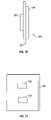
- FIG. 8is a diagram schematically illustrating a mobile phone with a clamshell-like structure that includes a sub-display disposed on an exterior surface of the clamshell.
- FIG. 9is a diagram schematically illustrating a mobile phone with a clamshell-like structure that includes a principle display disposed on an interior surface of the clamshell.
- FIG. 10is a diagram schematically illustrating a cross section of a backlight disposed between a principle display and a sub-display.
- FIG. 11is a diagram schematically illustrating light exit regions on a surface of a backlight.
- FIG. 12is a cross section schematically illustrating a display device that includes a backlight configured to illuminate a reflective sub-display and a principle display that is transmissive.
- FIG. 13Aschematically depicts a front view of an embodiment of a display device that includes a sub-display illuminated by a backlight through an annular light pipe that provides light to all sides of the sub-display.
- FIG. 13Bschematically depicts a perspective view of the annular light pipe, backlight, and sub-display of FIG. 13A .
- FIG. 13Cschematically depicts a perspective view of the annular light pipe of FIG. 13A .
- FIG. 14is a cross sectional view schematically illustrating an embodiment of a display device having a backlight that illuminates a reflective display using a light pipe.
- FIG. 15is a cross sectional view schematically illustrating an embodiment of a display device that includes a backlight that provides illumination to a sub-display via a backplate configured as a light pipe.
- FIG. 16is a cross sectional view schematically illustrating an embodiment of a display device that includes a backlight that provides illumination to a sub-display via a backplate configured as a light pipe and optical coupling material.
- FIG. 17is a cross sectional view schematically illustrating an embodiment of a display device that includes a substantially optically transmissive component disposed forward of a reflective display.
- FIG. 18is a cross sectional view schematically illustrating an embodiment of a display device illuminated by light spilled on a front surface of the display.
- FIG. 19is a cross sectional view schematically illustrating an embodiment of a display device illuminated by light distributed in a controlled manner on a front surface of the display.
- FIG. 20is a cross sectional view schematically illustrating an embodiment of a display device having first and second backplates that channel light to first and second reflective displays, respectively.
- FIG. 21schematically depicts an example of a spatial light modulator having scatter features or illumination dots.
- FIG. 22schematically depicts an embodiment of an illumination dot pattern used with a backlight.
- FIG. 23schematically depicts embodiments of possible positions for the array of illumination dots.
- FIG. 24is a flow chart showing different methods for manufacturing a spatial light modulator with illumination dots.
- the embodimentsmay be implemented in or associated with a variety of electronic devices such as, but not limited to, mobile telephones, wireless devices, personal data assistants (PDAs), hand-held or portable computers, GPS receivers/navigators, cameras, MP3 players, camcorders, game consoles, wrist watches, clocks, calculators, television monitors, flat panel displays, computer monitors, auto displays (e.g., odometer display, etc.), cockpit controls and/or displays, display of camera views (e.g., display of a rear view camera in a vehicle), electronic photographs, electronic billboards or signs, projectors, architectural structures, packaging, and aesthetic structures (e.g., display of images on a piece of jewelry).
- MEMS devices of similar structure to those described hereincan also be used in non-display applications such as in electronic switching devices.
- a displayincludes a transmissive display configured to be illuminated through a back surface and a reflective display configured to be illuminated through a front surface.
- the displayincludes a single light source sandwiched between the transmissive display and the reflective display. The light source illuminates the transmissive display through its back surface.
- a light pipereceives light from the light source and propagates the light so that it illuminates the reflective display through a front surface or edge of the display.
- the light pipe and the light sourceare possible depending on the application of the display.
- a cellular phoneis an example of a product in which the MEMS device can be used in a display.
- Cellular phones featuring a “clamshell-like” structureare typically closed when not in use and then opened to receive a telephone call.
- Such cellular phonesdo not allow viewing of a principle display located on an interior surface of the clamshell when the phone is closed. Consequently, a second smaller, less sophisticated display, which is sometimes referred to herein as a “sub-display,” can be included on an outer surface of the clamshell that is visible when the phone is closed to provide “quick-look” information without requiring a user to open the phone.
- the principle display and sub-displaycan be transmissive or transflective LCDs, which use backside illumination.
- a single backlight placed in-between the principle display and sub-displaycan be used to illuminate both displays.
- the backlightilluminates the principle display through a rear surface of the principle display.
- the backlightis configured with one or more light-leaking regions on its rear surface that correspond to the area of the sub-display.
- Light control patternsfor example, patterns on films attached to the backlight or patterns disposed directly on the backlight itself, can be used so that uniformity of light emitted from the front surface of the backlight is not disturbed by the loss of light that leaks out the rear surface to the sub-display.
- a reflective displaye.g., an interferometric modulator (MEMS device)
- MEMS deviceinterferometric modulator
- One solutionis to equip the reflective display with a frontlight. This solution works, but it has several undesirable consequences.
- the extra lightadds cost and complexity to the product.
- a front lightincreases the thickness of the display and the cell phone incorporating the display, and hence decreases the market desirability of the product.
- Methods and systemsinclude illuminating reflective displays using a single backlight to reduce the size and cost associated with adding an additional front light.
- Light from the backlightcan be channeled with a light pipe to a portion of the reflective display, such as an edge of the display or the front of the display.
- a backlightprovides rear illumination of a transmissive display located on one face of the clamshell, or portion thereof, and simultaneously provides front illumination of a reflective display, such as an interferometric modulator display, located on the opposite face of the clamshell, through light pipe structures.
- Light pipesmay be at least partially incorporated into the backplate of the reflective display, in some embodiments.
- a single light source with one or more light pipescan be used to illuminate reflective displays on both faces of the device.
- FIG. 1One interferometric modulator display embodiment comprising an interferometric MEMS display element is illustrated in FIG. 1 .
- the pixelsare in either a bright or dark state.
- the display elementIn the bright (“on” or “open”) state, the display element reflects a large portion of incident visible light to a user.
- the dark (“off” or “closed”) stateWhen in the dark (“off” or “closed”) state, the display element reflects little incident visible light to the user.
- the light reflectance properties of the “on” and “off” statesmay be reversed.
- MEMS pixelscan be configured to reflect predominantly at selected colors, allowing for a color display in addition to black and white.
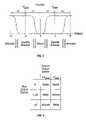
- FIG. 1is an isometric view depicting two adjacent pixels in a series of pixels of a visual display, wherein each pixel comprises a MEMS interferometric modulator.
- an interferometric modulator displaycomprises a row/column array of these interferometric modulators.
- Each interferometric modulatorincludes a pair of reflective layers positioned at a variable and controllable distance from each other to form a resonant optical cavity with at least one variable dimension.
- one of the reflective layersmay be moved between two positions. In the first position, referred to herein as the relaxed position, the movable reflective layer is positioned at a relatively large distance from a fixed partially reflective layer.
- the movable reflective layerIn the second position, referred to herein as the actuated position, the movable reflective layer is positioned more closely adjacent to the partially reflective layer. Incident light that reflects from the two layers interferes constructively or destructively depending on the position of the movable reflective layer, producing either an overall reflective or non-reflective state for each pixel.
- the depicted portion of the pixel array in FIG. 1includes two adjacent interferometric modulators 12 a and 12 b .
- a movable reflective layer 14 ais illustrated in a relaxed position at a predetermined distance from an optical stack 16 a , which includes a partially reflective layer.
- the movable reflective layer 14 bis illustrated in an actuated position adjacent to the optical stack 16 b.
- optical stack 16typically comprise of several fused layers, which can include an electrode layer, such as indium tin oxide (ITO), a partially reflective layer, such as chromium, and a transparent dielectric.
- ITOindium tin oxide
- the optical stack 16is thus electrically conductive, partially transparent and partially reflective, and may be fabricated, for example, by depositing one or more of the above layers onto a transparent substrate 20 .
- the layersare patterned into parallel strips, and may form row electrodes in a display device as described further below.
- the movable reflective layers 14 a , 14 bmay be formed as a series of parallel strips of a deposited metal layer or layers (orthogonal to the row electrodes of 16 a , 16 b ) deposited on top of posts 18 and an intervening sacrificial material deposited between the posts 18 . When the sacrificial material is etched away, the movable reflective layers 14 a , 14 b are separated from the optical stacks 16 a , 16 b by a defined gap 19 .
- a highly conductive and reflective materialsuch as aluminum may be used for the reflective layers 14 , and these strips may form column electrodes in a display device.
- the cavity 19remains between the movable reflective layer 14 a and optical stack 16 a , with the movable reflective layer 14 a in a mechanically relaxed state, as illustrated by the pixel 12 a in FIG. 1 .
- a potential differenceis applied to a selected row and column, the capacitor formed at the intersection of the row and column electrodes at the corresponding pixel becomes charged, and electrostatic forces pull the electrodes together.
- the movable reflective layer 14is deformed and is forced against the optical stack 16 .
- a dielectric layerwithin the optical stack 16 may prevent shorting and control the separation distance between layers 14 and 16 , as illustrated by pixel 12 b on the right in FIG. 1 .
- the behavioris the same regardless of the polarity of the applied potential difference. In this way, row/column actuation that can control the reflective vs. non-reflective pixel states is analogous in many ways to that used in conventional LCD and other display technologies.
- FIGS. 2 through 5Billustrate one exemplary process and system for using an array of interferometric modulators in a display application.
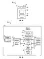
- FIG. 2is a system block diagram illustrating one embodiment of an electronic device that may incorporate aspects of the invention.
- the electronic deviceincludes a processor 21 which may be any general purpose single- or multi-chip microprocessor such as an ARM, Pentium®, Pentium II®, Pentium III®, Pentium IV®, Pentium® Pro, an 8051, a MIPS®, a Power PC®, an ALPHA®, or any special purpose microprocessor such as a digital signal processor, microcontroller, or a programmable gate array.
- the processor 21may be configured to execute one or more software modules.
- the processormay be configured to execute one or more software applications, including a web browser, a telephone application, an email program, or any other software application.
- the processor 21is also configured to communicate with an array driver 22 .
- the array driver 22includes a row driver circuit 24 and a column driver circuit 26 that provide signals to a panel or display array (display) 30 .
- the cross section of the array illustrated in FIG. 1is shown by the lines 1 - 1 in FIG. 2 .
- the row/column actuation protocolmay take advantage of a hysteresis property of these devices illustrated in FIG. 3 . It may require, for example, a 10 volt potential difference to cause a movable layer to deform from the relaxed state to the actuated state.
- the movable layermaintains its state as the voltage drops back below 10 volts.
- the movable layerdoes not relax completely until the voltage drops below 2 volts.
- There is thus a range of voltage, about 3 to 7 V in the example illustrated in FIG. 3where there exists a window of applied voltage within which the device is stable in either the relaxed or actuated state. This is referred to herein as the “hysteresis window” or “stability window.”
- the row/column actuation protocolcan be designed such that during row strobing, pixels in the strobed row that are to be actuated are exposed to a voltage difference of about 10 volts, and pixels that are to be relaxed are exposed to a voltage difference of close to zero volts. After the strobe, the pixels are exposed to a steady state voltage difference of about 5 volts such that they remain in whatever state the row strobe put them in. After being written, each pixel sees a potential difference within the “stability window” of 3-7 volts in this example. This feature makes the pixel design illustrated in FIG. 1 stable under the same applied voltage conditions in either an actuated or relaxed pre-existing state.
- each pixel of the interferometric modulatoris essentially a capacitor formed by the fixed and moving reflective layers, this stable state can be held at a voltage within the hysteresis window with almost no power dissipation. Essentially no current flows into the pixel if the applied potential is fixed.
- a display framemay be created by asserting the set of column electrodes in accordance with the desired set of actuated pixels in the first row.
- a row pulseis then applied to the row 1 electrode, actuating the pixels corresponding to the asserted column lines.
- the asserted set of column electrodesis then changed to correspond to the desired set of actuated pixels in the second row.
- a pulseis then applied to the row 2 electrode, actuating the appropriate pixels in row 2 in accordance with the asserted column electrodes.
- the row 1 pixelsare unaffected by the row 2 pulse, and remain in the state they were set to during the row 1 pulse. This may be repeated for the entire series of rows in a sequential fashion to produce the frame.
- the framesare refreshed and/or updated with new display data by continually repeating this process at some desired number of frames per second.
- protocols for driving row and column electrodes of pixel arrays to produce display framesare also well known and may be used in conjunction with the present invention.
- FIGS. 4 , 5 A and 5 Billustrate one possible actuation protocol for creating a display frame on the 3 ⁇ 3 array of FIG. 2 .
- FIG. 4illustrates a possible set of column and row voltage levels that may be used for pixels exhibiting the hysteresis curves of FIG. 3 .
- actuating a pixelinvolves setting the appropriate column to ⁇ V bias , and the appropriate row to +?V, which may correspond to ⁇ 5 volts and +5 volts respectively Relaxing the pixel is accomplished by setting the appropriate column to +V bias , and the appropriate row to the same +?V, producing a zero volt potential difference across the pixel.
- the pixelsare stable in whatever state they were originally in, regardless of whether the column is at +V bias , or ⁇ V bias .
- voltages of opposite polarity than those described abovecan be used, e.g., actuating a pixel can involve setting the appropriate column to +V bias , and the appropriate row to ⁇ ?V.
- releasing the pixelis accomplished by setting the appropriate column to ⁇ V bias , and the appropriate row to the same ⁇ ?V, producing a zero volt potential difference across the pixel.
- FIG. 5Bis a timing diagram showing a series of row and column signals applied to the 3 ⁇ 3 array of FIG. 2 which will result in the display arrangement illustrated in FIG. 5A , where actuated pixels are non-reflective.
- the pixelsPrior to writing the frame illustrated in FIG. 5A , the pixels can be in any state, and in this example, all the rows are at 0 volts, and all the columns are at +5 volts. With these applied voltages, all pixels are stable in their existing actuated or relaxed states.
- pixels ( 1 , 1 ), ( 1 , 2 ), ( 2 , 2 ), ( 3 , 2 ) and ( 3 , 3 )are actuated.
- columns 1 and 2are set to ⁇ 5 volts
- column 3is set to +5 volts. This does not change the state of any pixels, because all the pixels remain in the 3-7 volt stability window.
- Row 1is then strobed with a pulse that goes from 0, up to 5 volts, and back to zero. This actuates the ( 1 , 1 ) and ( 1 , 2 ) pixels and relaxes the ( 1 , 3 ) pixel. No other pixels in the array are affected.
- row 2is set to ⁇ 5 volts, and columns 1 and 3 are set to +5 volts.
- the same strobe applied to row 2will then actuate pixel ( 2 , 2 ) and relax pixels ( 2 , 1 ) and ( 2 , 3 ). Again, no other pixels of the array are affected.
- Row 3is similarly set by setting columns 2 and 3 to ⁇ 5 volts, and column 1 to +5 volts.
- the row 3strobe sets the row 3 pixels as shown in FIG. 5A . After writing the frame, the row potentials are zero, and the column potentials can remain at either +5 or ⁇ 5 volts, and the display is then stable in the arrangement of FIG. 5A .
- FIGS. 6A and 6Bare system block diagrams illustrating an embodiment of a display device 40 .
- the display device 40can be, for example, a cellular or mobile telephone.
- the same components of display device 40 or slight variations thereofare also illustrative of various types of display devices such as televisions and portable media players.
- the display device 40includes a housing 41 , a display 30 , an antenna 43 , a speaker 45 , an input device 48 , and a microphone 46 .
- the housing 41is generally formed from any of a variety of manufacturing processes as are well known to those of skill in the art, including injection molding, and vacuum forming.
- the housing 41may be made from any of a variety of materials, including but not limited to plastic, metal, glass, rubber, and ceramic, or a combination thereof.
- the housing 41includes removable portions (not shown) that may be interchanged with other removable portions of different color, or containing different logos, pictures, or symbols.
- the display 30 of exemplary display device 40may be any of a variety of displays, including a bi-stable display, as described herein.
- the display 30includes a flat-panel display, such as plasma, EL, OLED, STN LCD, or TFT LCD as described above, or a non-flat-panel display, such as a CRT or other tube device, as is well known to those of skill in the art.
- the display 30includes an interferometric modulator display, as described herein.
- the components of one embodiment of exemplary display device 40are schematically illustrated in FIG. 6B .
- the illustrated exemplary display device 40includes a housing 41 and can include additional components at least partially enclosed therein.
- the exemplary display device 40includes a network interface 27 that includes an antenna 43 which is coupled to a transceiver 47 .
- the transceiver 47is connected to the processor 21 , which is connected to conditioning hardware 52 .
- the conditioning hardware 52may be configured to condition a signal (e.g. filter a signal).
- the conditioning hardware 52is connected to a speaker 45 and a microphone 46 .
- the processor 21is also connected to an input device 48 and a driver controller 29 .
- the driver controller 29is coupled to a frame buffer 28 and to the array driver 22 , which in turn is coupled to a display array 30 .
- a power supply 50provides power to all components as required by the particular exemplary display device 40 design.
- the network interface 27includes the antenna 43 and the transceiver 47 so that the exemplary display device 40 can communicate with one ore more devices over a network. In one embodiment the network interface 27 may also have some processing capabilities to relieve requirements of the processor 21 .
- the antenna 43is any antenna known to those of skill in the art for transmitting and receiving signals. In one embodiment, the antenna transmits and receives RF signals according to the IEEE 802.11 standard, including IEEE 802.11(a), (b), or (g). In another embodiment, the antenna transmits and receives RF signals according to the BLUETOOTH standard. In the case of a cellular telephone, the antenna is designed to receive CDMA, GSM, AMPS or other known signals that are used to communicate within a wireless cell phone network.
- the transceiver 47pre-processes the signals received from the antenna 43 so that they may be received by and further manipulated by the processor 21 .
- the transceiver 47also processes signals received from the processor 21 so that they may be transmitted from the exemplary display device 40 via the antenna 43 .
- the transceiver 47can be replaced by a receiver.
- network interface 27can be replaced by an image source, which can store or generate image data to be sent to the processor 21 .
- the image sourcecan be a digital video disc (DVD) or a hard-disc drive that contains image data, or a software module that generates image data.
- Processor 21generally controls the overall operation of the exemplary display device 40 .
- the processor 21receives data, such as compressed image data from the network interface 27 or an image source, and processes the data into raw image data or into a format that is readily processed into raw image data.
- the processor 21then sends the processed data to the driver controller 29 or to frame buffer 28 for storage.
- Raw datatypically refers to the information that identifies the image characteristics at each location within an image. For example, such image characteristics can include color, saturation, and gray-scale level.
- the processor 21includes a microcontroller, CPU, or logic unit to control operation of the exemplary display device 40 .
- Conditioning hardware 52generally includes amplifiers and filters for transmitting signals to the speaker 45 , and for receiving signals from the microphone 46 .
- Conditioning hardware 52may be discrete components within the exemplary display device 40 , or may be incorporated within the processor 21 or other components.
- the driver controller 29takes the raw image data generated by the processor 21 either directly from the processor 21 or from the frame buffer 28 and reformats the raw image data appropriately for high speed transmission to the array driver 22 . Specifically, the driver controller 29 reformats the raw image data into a data flow having a raster-like format, such that it has a time order suitable for scanning across the display array 30 . Then the driver controller 29 sends the formatted information to the array driver 22 .
- a driver controller 29such as a LCD controller, is often associated with the system processor 21 as a stand-alone Integrated Circuit (IC), such controllers may be implemented in many ways. They may be embedded in the processor 21 as hardware, embedded in the processor 21 as software, or fully integrated in hardware with the array driver 22 .
- the array driver 22receives the formatted information from the driver controller 29 and reformats the video data into a parallel set of waveforms that are applied many times per second to the hundreds and sometimes thousands of leads coming from the display's x-y matrix of pixels.
- driver controller 29is a conventional display controller or a bi-stable display controller (e.g., an interferometric modulator controller).
- array driver 22is a conventional driver or a bi-stable display driver (e.g., an interferometric modulator display).
- a driver controller 29is integrated with the array driver 22 .
- display array 30is a typical display array or a bi-stable display array (e.g., a display including an array of interferometric modulators).
- the input device 48allows a user to control the operation of the exemplary display device 40 .
- input device 48includes a keypad, such as a QWERTY keyboard or a telephone keypad, a button, a switch, a touch-sensitive screen, a pressure- or heat-sensitive membrane.
- the microphone 46is an input device for the exemplary display device 40 . When the microphone 46 is used to input data to the device, voice commands may be provided by a user for controlling operations of the exemplary display device 40 .
- Power supply 50can include a variety of energy storage devices as are well known in the art.
- power supply 50is a rechargeable battery, such as a nickel-cadmium battery or a lithium ion battery.
- power supply 50is a renewable energy source, a capacitor, or a solar cell, including a plastic solar cell, and solar-cell paint.
- power supply 50is configured to receive power from a wall outlet.
- control programmabilityresides, as described above, in a driver controller which can be located in several places in the electronic display system. In some cases control programmability resides in the array driver 22 . Those of skill in the art will recognize that the above-described optimization may be implemented in any number of hardware and/or software components and in various configurations.
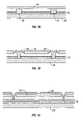
- FIGS. 7A-7Eillustrate five different embodiments of the movable reflective layer 14 and its supporting structures.
- FIG. 7Ais a cross section of the embodiment of FIG. 1 , where a strip of metal material 14 is deposited on orthogonally extending supports 18 .
- FIG. 7Bthe moveable reflective layer 14 is attached to supports at the corners only, on tethers 32 .
- FIG. 7Cthe moveable reflective layer 14 is suspended from a deformable layer 34 , which may comprise a flexible metal.
- the deformable layer 34connects, directly or indirectly, to the substrate 20 around the perimeter of the deformable layer 34 .
- connection postsare herein referred to as support posts.
- the embodiment illustrated in FIG. 7Dhas support post plugs 42 upon which the deformable layer 34 rests.
- the movable reflective layer 14remains suspended over the cavity, as in FIGS. 7A-7C , but the deformable layer 34 does not form the support posts by filling holes between the deformable layer 34 and the optical stack 16 . Rather, the support posts are formed of a planarization material, which is used to form support post plugs 42 .
- the embodiment illustrated in FIG. 7Eis based on the embodiment shown in FIG. 7D , but may also be adapted to work with any of the embodiments illustrated in FIGS. 7A-7C as well as additional embodiments not shown. In the embodiment shown in FIG. 7E , an extra layer of metal or other conductive material has been used to form a bus structure 44 . This allows signal routing along the back of the interferometric modulators, eliminating a number of electrodes that may otherwise have had to be formed on the substrate 20 .
- the interferometric modulatorsfunction as direct-view devices, in which images are viewed from the front side of the transparent substrate 20 , the side opposite to that upon which the modulator is arranged.
- the reflective layer 14optically shields some portions of the interferometric modulator on the side of the reflective layer opposite the substrate 20 , including the deformable layer 34 and the bus structure 44 . This allows the shielded areas to be configured and operated upon without negatively affecting the image quality.
- This separable modulator architectureallows the structural design and materials used for the electromechanical aspects and the optical aspects of the modulator to be selected and to function independently of each other.
- FIGS. 7A-7Ethe embodiments shown in FIGS.
- the “clamshell” cell phone 82there are many mobile devices, e.g., the “clamshell” cell phone 82 , that include a principle display 84 located on an inner surface of one half of the clamshell, and a sub-display 80 located on an outer surface of the same half of clamshell as the principle display 84 .
- Examples of reflective devices which can be used as the principle display 84 and the sub-display 80include LCD's and interferometric modulators.
- the principle display 84 and/or the sub-display 80can comprise interferometric modulators. If the principle display 84 and the sub-display 80 are both reflective devices, they may benefit from receiving additional illumination when ambient light is not sufficient to view displayed information.
- Examples of devices for providing additional illuminationinclude light emitting diodes (LEDs), incandescent lamps, and fluorescent lamps. Approaches that are described herein for providing light to the principle display 84 can also be used to provide light to the sub-display 80 , and vice-versa.
- LEDslight emitting diodes
- incandescent lampsincandescent lamps
- fluorescent lampsfluorescent lamps.
- FIG. 10shows one embodiment of a dual display 100 where a backlight light source 90 is used to provide light to a principle display 84 and a sub-display 80 .
- both the principle display 84 and the sub-display 80can be, e.g., LCD devices that allow light from the backlight 90 to enter the principle display 84 and the sub-display 80 through the back of the displays by using configured light leaks to the LCD devices.
- Providing illumination from a common backlight 90 to both displaysis efficient when the displays are configurable to allow light to enter the devices from behind, e.g., through a portion of the back panel of the display device.
- the displays 84 and 80can also be reflective devices.
- the backlight 90may include light leak areas or channels specifically designed to allow light to propagate directly from the backlight 90 to the front surface of the displays 80 , 84 thereby front lighting the displays 84 , 80 .
- Other embodimentsmay incorporate more than one light source to illuminate the displays 84 , 80 .
- FIGS. 11 and 12illustrate an embodiment of a dual display 100 that includes a backlight 90 that provides light to a principle display 84 and a reflective sub-display 80 via first and second light pipes 112 , 114 .
- the aperture for the light leak regions 102 , 104 in a backlightcan vary in size and shape.
- the light leak regioncan substantially match the size of the area of the sub-display 80 , or substantially match the shape of the sub-display 80 , or be larger than the size of the perimeter of the sub-display 80 , as described in reference to FIG. 13 .
- the number of apertures or light leak regions 102 , 104 disposed on the backlight 90can vary.
- a light leakmay be created, for example, by removing portions of a reflective backing on the back of a backlight to create an aperture.
- an optically transmissive materialmay be placed in the aperture of the light leak region 102 , 104 .
- the light leak regions 102 , 104are not limited in location to the back of the backlight, they may be located in any region of the backlight which does not interfere with the lighting or viewing of the principle display 84 .
- the light leak regions 102 , 104are disposed on the backlight 90 in the region behind the sub-display.
- the light-leak regionsmay be placed on the backlight directly behind the sub-display and/or in a region above, below or to the side or sides of the area directly behind the sub-display (see, e.g., FIG. 11 ).
- lightcan exit the backlight through a side surface of the backlight 90 (not shown), or through a portion of the surface of the backlight 90 facing but not covered by the principle display 84 .
- the light from the light leak regions 102 , 104can be provided to the sub-display 80 via an optical medium such as the first and second light pipes 112 , 114 .
- the dual display device 100 shown in FIG. 12comprises a backlight 90 illuminating a principle display 84 that is disposed on one side of the backlight 90 , and a sub-display 80 disposed on the opposite side of the backlight 90 .
- the sub-display 80 shown in FIG. 12includes a backplate 116 and is optically coupled to light pipes 112 , 114 .
- the light leak regions 102 , 104( FIG.
- the light pipes 112 , 114can be covered by light pipes 112 , 114 ( FIG. 12 ) so that light propagates from the backlight 90 into the light pipes 112 , 114 .
- the light pipes 112 , 114are also coupled to a front surface edge of the sub-display 80 .
- the light pipes 112 , 114comprise material that is substantially optically transmissive such as, for example, polycarbonate or acrylic plastic materials.
- the light pipes 112 , 114can include, for example, a solid light guide that guides the light via total internal reflection (TIR).
- the light pipes 112 , 114include a fiber optic such as a fiber optical bundle.
- the light pipes 112 , 114can also be hollow, and have reflective (e.g., metallized) surfaces to propagate light through the hollow region therein. Other designs of light pipes are also possible.
- the light from the light source 90can couple directly into the light pipe 112 , 114 .
- An emitting surface of the light source 90can be disposed close to or possibly in contact with an input surface 111 of the light pipe 112 , 114 to increase coupling efficiency.
- the entrance 111lies in the plane of the backlight 90 , corresponding to the light leak region 104 of the backlight 90 .
- the light from the light source 90can be coupled into the light pipe 112 , 114 through an intermediate component or material.
- This optically transmissive light piping 112 , 114is configured to propagate light from the backlight light source 90 to the sub-display 80 , to for example, a side or a portion of a side of the sub-display 80 or to a surface or a portion of a surface of the sub-display 80 .
- the light pipealso has an exit area 118 where light is output coupled and transferred from the light pipe 114 to the sub-display 80 .
- the sub-display 80may include an optically transmissive substrate (for example, illustrated as substrate 20 in FIG. 1 ). As discussed more fully below in reference to FIG. 17 , in some embodiments, the sub-display 80 can have a frontplate (for example, optical plate 152 in FIG. 17 ) disposed in front of the substrate. In various embodiments, the light pipe is optically coupled to the substrate and/or the front plate.
- the exit face or aperture 118is oriented generally perpendicular to the entrance face or aperture 111 .
- This exit 118may be disposed close to the edge of the frontplate and/or substrate of the sub-display 80 . In this way, light that leaks from the backlight 90 is output coupled into the edge of the frontplate and/or substrate, either or both of which may optically guide the light therein.
- a single light pipe 112provides light to the sub-display 80 .
- two or more light pipes 112 , 114provide light to the sub-display 80 .
- the lightcan enter the sub-display 80 at particular points. The light can be spread across the display 80 using various spreading or distribution techniques as discussed more fully below. Light can be provided to the sub-display 80 along one or more edges of the sub-display 80 by configuring one or more of the light pipes 112 , 114 to contact the sub-display 80 along a portion of or all of the edge of the sub-display 80 .
- a light pipemay be configured to couple light from the backlight 90 to the substrate or to a frontplate disposed forward of the substrate.
- the substrate or frontplatecan include optical features that help to re-direct light to the light modulating element of the sub-display 80 .
- optical features on a surface of the substrate or a frontplate or in the substrate or frontplatemay redirect light guided through the substrate or frontplate.
- optical features on the surface or in the substrate or frontplatecan redirect light incident on the substrate or frontplate at grazing incidence, which would otherwise not be transmitted through the frontplate or substrate, to the light modulating element of the display.
- optical featuresmay comprise, for example, scatter features that scatter light or micro-optical elements including but not limited to mini-prisms and micro-lenses that redirect light.
- the optical featurescan comprise molded optics. Accordingly, the optical features may operate on the light in a deterministic or non-deterministic fashion.
- These optical featuresmay comprise one or more surfaces that reflect or refract light (similar, for example, to those in a Fresnel lens or a corner turning film) to redirect the light toward the light modulating elements.
- the optical elementsmay be symmetric or asymmetric and may be periodic and/or non-periodic. Together the optical elements may form, for example a hologram or diffractive optical element or a diffuser.
- optical elementsneed not be limited to surfaces features and may include volume features such as in a bulk diffuser or hologram. Accordingly, the light can be redirected using reflection, refraction, diffraction, diffusion, random or pseudo-random scattering techniques, or any combination thereof. Other configurations and approaches are also possible.
- the optical couplingsmay provide index matching to reduce reflection at the interface between the light pipe and the substrate.
- the exit port of the light pipes 112 , 114have a numerical aperture or etendue that substantially matches the numerical aperture or etendue of the substrate.
- optical couplingprovides a numerical aperture or etendue that matches that of the substrate. This optical coupling may, for example, alter the numerical aperture or etendue of the light pipe 112 , 114 to substantially match that of the substrate.
- An imaging or non-imaging optical componentmay, for example, be used to achieve this conversion of numerical aperture or etendue.
- the end of the light pipe 112 , 114is shaped and configured to provide this conversion.
- the optical couplingsmay provide index matching to reduce reflection.
- etenduemay be substantially matched to increase or maximize throughput.
- the light pipes 112 , 114are coupled to both the substrate and one or more optical plate, sheet, layer, or film thereon, etendue may be substantially matched as well to increase throughput.
- FIGS. 13A-Cillustrate another embodiment of a display device 120 where an annular light pipe 122 provides light from the backlight 90 to the edges of the sub-display 80 .
- FIG. 13Aschematically depicts a front view of an embodiment of the annular light pipe 122 mounted on the backlight 90 with the sub-display 80 inserted in the center of the annular light pipe 122 . In this configuration, light is provided by the backlight 90 to all sides of the sub-display through the annular light pipe 122 .
- FIG. 13Bschematically depicts a perspective view of the annular light pipe and backlight of FIG. 13A where the sub-display 80 is shown inset in the annular light pipe 122 .
- FIG. 13Cschematically depicts the annular light pipe of FIG. 13A without the sub-display 80 and illustrates the exit ports 118 of the annular light pipe.
- the annular light pipe 122has a light entrance (not shown) which could vary in size or location.
- the entrance of the light pipe 122has inner dimensions that are approximately the same shape and size, or slightly larger or smaller, as the outline of the sub-display 80 .
- the area of the entrance into the annular light pipe 122can correspond with the shape and size of a light-leak region on the backlight 90 .
- the annular light pipe 122is shaped to conform and provide light to the four edges of the sub-display 80 .
- the light pipe 122is configured such that the exit portion 118 of the annular light pipe can propagate light into portions of the edges of the sub-display 80 .
- the size of the entrance of the light pipemay vary and can have a cross-sectional area that is the same, larger or smaller than the cross-sectional area of the exit of the light pipe.
- the entrance and exit of the light pipeare configured so light efficiently enters the light pipe 122 , propagates through and exits the light pipe with reduced or minimal light loss.
- some light that does not initially exit the light pipe through the light pipe exitmay be recycled back through the light pipe and into the backlight 90 . This recycled light may pass through the backlight 90 to illuminate the principle display or re-enter the light pipe 122 so as to ultimately illuminate the sub-display 80 .
- the light pipe 122may comprise a solid or hollow optical pipe or a fiber or fiber bundle, and other variations are also possible.
- the light pipemay comprise polymer material that can be molded, for example, by injection molding in some embodiments. Other methods of fabricating the annular light pipe 122 may be used.
- the annular light pipe 122can be configured to be an attachment device that secures the sub-display 80 in the display device 120 and is optically coupled to the sub-display 80 .
- FIG. 14illustrates illumination of a dual display device with the back of principle display 84 facing the back of the sub-display 80 , wherein the principle display 84 is illuminated from a light source 191 at the edge of the principle display 84 .
- the sub-display 80is illuminated at the edge of the display from the same light source 191 through a light pipe 193 .
- the light pipe 193is optically coupled 154 to the edge of the sub-display 80 to disperse the light evenly throughout the sub-display 80 .
- optical coupling 154couples the light pipe 193 to the sub-display 80 .
- the principle display 84can be any type of display that is configured to be illuminated on the edge of the display.
- the sub-display 80 and/or the principle display 84have scattering features or other optical structures disposed on or forward of the display, for example, on a surface between the viewer and the reflective light modulating portion of the sub-display 80 or the principle display 84 .
- the backplate of the sub-displaycan be used as part or all of the light pipe.
- the light-leak from the backlightcan, for example, comprise an area defined by the area of the sub-display, e.g., essentially square or rectangular. Two examples are shown in FIGS. 15 and 16 where areas of light transfer are indicated by hatching at the light entrance 132 .
- the backplate 134 of the sub-display 80can be modified to operate as the light pipe. In some embodiments where the backplate 134 serves as a light pipe, the backplate may have similar features to the light pipes 112 , 114 and annular light pipe 122 discussed above.
- the backplate 134may comprise optically transmissive material through which light can propagate.
- the backplate 134may, for example, comprise polymeric material that is molded or formed into a suitable shape, e.g., to surround and hold the sub-display 80 and to optically couple to the light leakage region 132 .
- the backplatemay include a hollow region through which light may propagate.
- the backplatemay be optically coupled to the sub-display 80 , or coupled to a sheet, plate, or film proximal to the display, for example, through an optical cement.
- the backplate 134may be disposed about the display 80 to produce a cavity between the display and backplate.
- the backplate 134 of the sub-display 80is configured as a light pipe that receives light through a light entrance 132 and propagates the light to the front edge of the sub-display 80 , where the light exits the backplate/lightpipe 134 through the light exits 136 , 138 and enters the sub-display 80 .
- the backplate 134can be configured in various ways to provide light to a portion of the edge or the entire edge of the sub-display 80 .
- the backplate 134can be extended beyond the edges of the sub-display 80 , and disposed such that the light exit area of the backplate 134 is near the edge of the sub-display 80 .
- optical couplings 142 , 144can be used to optically bridge any gap that exists between the light exit area of the backplate 134 and the sub-display 80 .
- the optical coupling 142 , 144can be, for example, a small light pipe or optical coupling adhesive.
- the optical couplings 142 , 144may include reflective surfaces therein to direct light from the backplate 134 into the display. In this way, the combination of the backplate 134 and the optical couplings 142 , 144 serves as the light pipe that provides light from the backlight 90 to the sub-display 80 .
- FIG. 17shows a substantially optically transmissive component 152 disposed forward of the sub-display 80 .
- the substantially optically transmissive componentis an optical plate, and in the discussion of an embodiment hereinbelow, the substantially optically transmissive component will be referred to as optical plate 152 .
- the substantially optically transmissive componentis an optical sheet, film or layer.
- the substantially optically transmissive componentcomprises a light guide. Accordingly, the discussion provided herein with respect to the optical plate 152 may also apply to optical sheets, films, and layers as well.
- the light pipe 112 , 114may be configured to couple light from the backlight 90 to the optical plate 152 disposed forward of the sub-display 80 (for example, between the sub-display 80 and a viewer of the sub-display 80 ).
- the optical plate 152can include optical features that help to re-direct light to the light modulating element of the sub-display 80 .
- optical features on a surface of the optical plate 152 or in the optical plate 152may redirect light guided through the optical plate 152 , e.g., by total internal reflection.
- optical features on the surface or in the optical plate 152can redirect light incident on the optical plate 152 at or near grazing incidence. This redirected light, which would otherwise not be transmitted through the optical plate 152 , is made to impinge upon and illuminate the light modulating elements of the display.
- These optical featuresmay comprise, for example, scatter features that scatter light or micro-optical elements including but not limited to mini-prisms and micro-lenses that redirect light.
- the optical featurescan comprise molded optics. Accordingly, the optical features may operate on the light in a deterministic or non-deterministic fashion.
- optical featuresmay comprise one or more surfaces that reflect or refract light (similar, for example, to those in a Fresnel lens or a corner turning film, e.g., a variation of the quarter turning film by 3M Corporation) to redirect the light toward the light modulating elements.
- the optical elementsmay be symmetric or asymmetric and may be periodic and/or non-periodic. Together the optical elements may form, for example a hologram or diffractive optical element or a diffuser.
- These optical elementsneed not be limited to surfaces features and may include volume features such as in a bulk diffuser or hologram. Accordingly, the light can be redirected using reflection, refraction, diffraction, diffusion, random or pseudo-random scattering techniques, or any combination thereof. Other configurations and approaches are also possible.
- the optical plate 152may comprise, for example, glass or plastic or any substantially optically transmissive (or transparent) material.
- the optical plate 152comprises an optical sheet, film or layer.
- Such an optical sheet, film, or layermay also comprise, e.g., glass or polymer or other substantially optically transmissive material.
- an optical film 152is laminated to the substrate on which the spatial light modulator elements are formed on one or more layers thereon.
- the optical film 152can be grown or may be formed in other ways, for example, optical structures may be molded directly onto the sub-display as a permanent or removable optical film.
- the optical plate 152can be optically coupled to the light pipes 112 , 114 by a variety of techniques.
- optical adhesive or other coupling materialmay be used as optical coupling 154 , 156 , or the light pipe 112 , 114 may be near or touching the optical plate 152 .
- the optical coupling 154 , 156may provide index matching to reduce reflection at the interface between the light pipes 112 , 114 and the optical plate 152 .
- the exit port of the light pipes 112 , 114have a numerical aperture or etendue that substantially matches the numerical aperture or etendue of the optical plate 152 .
- optical coupling 114 , 156provides a numerical aperture or etendue that matches that of the optical plate 152 .
- This optical couplingmay, for example, alter the numerical aperture or etendue of the light pipe to substantially match that of the optical plate 152 .
- An imaging or a non-imaging optical componentmay, for example, be used to achieve this conversion of numerical aperture or etendue.
- the ends of the light pipes 112 , 114are shaped and configured to provide this conversion.
- the optical plate 152may be configured to disperse the light from the light pipes 112 , 114 evenly throughout the sub-display surface.
- the backplate 116comprises a light pipe that couples light into the optical plate 152 .
- FIG. 18illustrates an embodiment where the light pipes 112 , 114 spill the light 162 onto the sub-display 80 or onto an optical plate (sheet, film, or layer, etc.), such as the optical plate 152 shown in FIG. 17 .
- the shape of the light pipe and the shape of the exit regionscan be tailored to distribute light in a controlled manner.
- the sub-display 80 or optical plate 152may be configured to disperse the light throughout the display.
- Optical featuresmay be used to re-direct light toward the light modulating elements, as discussed above. See, for example, discussion of FIG. 17 an associated discussion.
- FIG. 19illustrates an embodiment where the light pipes 112 , 114 further comprise distal portions 164 , 166 configured to control the distribution of light, e.g., distribute light 168 onto the sub-display 80 in a pre-determined pattern.
- the distal portion 164 , 166 of the optical pipes 112 , 114can be structured to mimic edge lighting with LEDs. Knowledge of the pattern of the structured spill allows the sub-display 80 to be configured so as to disperse the light evenly throughout the display with, for example, optical features in the display, one or more optical plates 152 (or sheets, films, or layers) as discussed with reference to FIG. 17 .
- the distal portion 164 , 166 of the optical light pipes 112 , 114can be separate components optically coupled to the light pipes 112 , 114 , or the distal portions 164 , 166 may be integrated as part of the light pipes 112 , 114 .
- FIG. 20illustrates a dual display outfitted with first and second light sources 192 , 194 disposed between the sub-display 80 and a principle display 182 .
- Light pipes 181 , 183 , 185 , 187optically couple the light sources 192 , 194 to the backplates 116 , 117 , which are also light guides.
- the lightis further funneled by additional optical pipes 186 , 188 , 196 , 198 to the displays 80 , 84 .
- the additional optical pipes 186 , 188 , 196 , 198are optically coupled to an optical film or plate 174 , 184 disposed forward at the displays 80 , 84 .
- the optical films or plates 174 , 184may comprise optical features to redirect light toward the light modulating elements as discussed above.
- the light pipes 186 , 188 , 196 , 198 and optical plate 152 , 184may be optically coupled in a manner that increases the transfer of light.
- the additional optical pipes 181 , 183 , 185 , 187 , 186 , 188 , 196 , 198 and/or optical plates or films 174 , 184are not used, and the backplates 116 , 117 are configured to propagate the light from light sources 192 , 194 either throughout the displays 80 , 182 or to the edge of the displays which may comprise scatter features.
- lightmay be coupled by light pipes into the substrate in addition to or instead of the optical films or plates 174 , 184 .
- a wide range of variations in configuration and designs such as discussed above and elsewhere hereinmay be employed.
- the display device of claim 30wherein the light piping comprises a single backplate that provides light to both the first and second displays. Still other variations are possible as well.
- dual display devicescan include features that re-direct (e.g., scatter) light to the reflective display.
- Such featuresmay comprise, for example, illumination dots, described in the commonly owned patent application entitled “Integrated Modulator Illumination,” U.S. patent application Ser. No. 10/794,825.
- FIG. 21An embodiment of a purely reflective display comprising a spatial light modulator having illumination dots is shown in FIG. 21 .
- the spatial light modulator in this examplecomprises interferometric modulators such as described above used as part of the dual display device.
- a diffuser 206is disposed forward of the spatial light modulator.
- the interferometric modulator shown in FIG. 21is formed on an optically transmissive substrate 200 .
- Each element 204 of the spatial light modulator arraycan be individually activated to modulate the light that travels through the diffuser 206 and through the substrate 200 to reach the element 204 .
- Each modulator elementwhen activated, can be used to direct modulated or non-modulated light to a viewer 214 on the opposite side of the substrate 200 .
- This embodimentincludes a backplate 202 for the modulator that can be opaque, rendering this type of modulator difficult to use with backlighting.
- the elements 204are themselves opaque, which makes backlighting even more difficult.
- illumination dots 208 formed at the interface between the diffuser 206 and the substrate 200can provide illumination for the display.
- Each dot 208is comprised of a first layer 210 that is reflective disposed towards the modulator array and a second layer 212 that is absorbing disposed towards the viewer 214 .
- the illumination dotsmay be formed on the surface of the optically transmissive substrate 200 or on the diffuser 206 (or on one or more layers formed or coupled thereon, e.g., an optical plate 152 ) by various types of printing or thin film deposition techniques. Other methods of forming the optical features may also be employed.
- FIG. 21shows a light source 216 , such as a cold cathode fluorescent tube or a light emitting diode (LED), residing at one edge of the optically transmissive substrate 200 .
- a light source 216such as a cold cathode fluorescent tube or a light emitting diode (LED)
- LEDlight emitting diode
- Light emitted by the light source 216 and properly injected into the substrate 200propagates through the substrate guided therein by total internal reflection.
- the light source 216 in FIG. 21can be a light pipe that illuminates the edge of the display, or that illuminates an optical plate, sheet, film, or layer forward of the display.
- the dotscan be configured and arranged depending, for example, upon the type and distribution of the illumination and the environment in which the modulator may be used as well as the design of the spatial light modulator.
- FIG. 22shows an example of a dot pattern that is not uniform.
- the dot arrangementmay vary in many aspects and may be, for example, irregular.
- the degree of regularity of the arrangement of dotsmay range from completely random, to partially random and partially regular to uniform and periodic.
- the arrangementmay be selected to reduce Moire effects that result from the periodicity of the light modulating elements in the modulator array or to reduce fixed pattern noise.
- the dotscan be arranged to distribute the light in a particular fashion, for example, evenly across the display for a given illumination configuration.
- Dots in the dot patterndeflect or scatter light which subsequently strikes modulator elements such as elements 304 a and 304 b .
- the light deflected or scattered from dot 302may have been internally reflected several times within substrate 200 before striking dot 302 and being deflected or scattered.
- the dotsmay be arranged in a pattern to provide for a specific distribution of light on the spatial light modulator array. In some embodiments, for example, the dot pattern can create uniform illumination on the array of spatial light modulator elements.
- the dotswill be of a size too small to resolve by the vision of a human observer viewing the display at a normal viewing distance.
- Undesirable artifactscan sometimes still be created by arrays with features that are not individually resolvable.
- the patterncan be such that these undesirable artifacts are mitigated or eliminated.
- the patterncan also control the distribution of the light on the spatial light modulators.
- the surface upon which the dots are placedmay also be varied.
- the dotsare shown at the interface between the diffuser 502 and the optically transmissive substrate 500 .
- the diffuser 502is mated to the optically transmissive substrate 500 in certain embodiments.
- the diffuserhas been lifted away from the substrate 500 .
- the dotscould be patterned onto the surface of the substrate 500 , such as dot 504 .
- Dot 504has a reflective portion 508 towards the modulator array, not shown, and an absorbing portion 506 towards the viewer 214 .
- the dotscan be placed on the surface of the diffuser 502 , such as dot 510 .
- the dotscan also be formed on one or more layers on the diffuser 502 or substrate 500 or can be formed elsewhere (e.g., on an optical plate disposed between the reflective display and a viewer of the display). Changing the position of the dots may modify the dot processing sequence.
- a dot on the surface of the substrate, such as 504may have a first reflective material 508 deposited and then covered by an ‘overcoat’ 506 of absorbing material. If the dots reside on the surface of the diffuser 502 , such as 510 , the absorbing material 512 may be put down first, followed by the reflective material 514 . This approach maintains the proper orientation of the layers with regards to the modulator and the viewer 214 .
- optical featurescan be located elsewhere.
- the optical featuresmay be disposed on the surface of an optical plate (sheet, film, or layer).
- the optical featuresmay also be disposed in the substrate or optical plate (sheet, film, or layer). Still other variations are possible.
- dots having a specific shape and configurationare shown in FIGS. 21-23 , other types of features may be used in the substrate of the sub-display or an optical plate, sheet or film forward the sub-display.
- These featuresmay, for example, comprise microstructures or microstructure arrays comprising, e.g., bumps, dots, or pits.
- the featuresmay comprise concave or convex surfaces (e.g., that form lenses or lenlets).
- the featuresare elongated and comprise, e.g., ribs, ridges, or grooves, that may or may not be straight. Tilted and curved surfaces may be used as well. A wide range of other shapes, geometries, and configurations are possible.
- the geometriesmay deterministically redirect the light into the display.
- micro-opticssuch as micro-lenses, prisms, and corner turning films may be used.
- the featuresmay, for example, redirect light disposed at any angle on the surface of the display to fold into the display for proper illumination.
- Non-deterministic approachesmay be employed.
- the optical featuresmay comprise features that form a diffuser, a diffractive optical element, or a hologram.
- the featuresmay have regular or irregular shape and may have different dimensions.
- the featuresmay comprise opaque or substantially optically transmissive material.
- the featuresmay be partially or completely reflective, transmissive, and/or absorbing.
- the featuresmay comprise metal in some embodiments or may comprise dielectric.
- the featuresmay comprise dielectric having an index of refraction that is the same or different than the surface (e.g., substrate, diffuser, optical plate, other layers etc.) on which the features are formed.
- Some microstructure arrayscan have dimensions on the order of microns.
- the featurescan be fabricated in different ways as well.
- the featurescan be applied, for example, by printing or lithographically, by injection molding or laser etching.
- the featurescan be applied onto a surface as a film.
- light scattering and/or directing microstructurescan be manufactured and bonded onto a surface of the display, optical film or plate using resin which is molded and cured to form a desired microstructure, for example using ultraviolet-setting resin. Other methods of fabricating the scattering features are also possible.
- the processstarts with providing a substantially optically transmissive substrate at block 600 .
- the illumination dotsare applied to the optically transmissive substrate or any optical plate, sheet or film 152 forward of the display at block 602 .
- the spatial light modulatoris manufactured at block 604 .
- the modulatoris finished at block 606 , which may include such tasks as attaching a backplate.
- the diffuseris applied to the substrate or any optical plate 152 , forward the display, over the illumination dots, at block 608 .
- Other componentsmay also be included.
- the spatial light modulatoris manufactured on the ‘back side’ (away from the viewer) of the substantially optically transmissive substrate at block 610 .
- the spatial light modulatoris finished at block 612 .
- the illumination dotsare applied to the front side of the substrate at block 614 and the diffuser is applied at block 616 .
- a diffuseris supplied at block 618 either after the modulator is finished at block 612 or in parallel with the process of manufacturing and finishing the modulator.
- the illumination dotsare applied to the diffuser at block 620 and the diffuser is applied to the substrate at block 622 .
- the optical featuresmay be formed in one of many printing procedures, including, e.g., lithographic printing, inkjet printing, screen-printing or any other type of printing technique. Non-printing based methods may also be used.
- the optical featurescan, for example, be embossed onto the surface or molded.
- the optical featuresmay be formed on a surface that is laminated or adhered to the substrate or optical plate or other layer. Still other techniques, including both those well known in the art as well as those yet to be devised may be employed.
- the shape and configurations of the optical featuresmay be controlled to increase or maximize effectiveness.
- the optical featurescan be fabricated at a resolution below the resolution of the human eye to avoid affecting the image quality as seen by the viewer.
Landscapes
- Physics & Mathematics (AREA)
- General Physics & Mathematics (AREA)
- Optics & Photonics (AREA)
- Nonlinear Science (AREA)
- Mathematical Physics (AREA)
- Chemical & Material Sciences (AREA)
- Crystallography & Structural Chemistry (AREA)
- Spectroscopy & Molecular Physics (AREA)
- Mechanical Light Control Or Optical Switches (AREA)
- Devices For Indicating Variable Information By Combining Individual Elements (AREA)
- Control Of Indicators Other Than Cathode Ray Tubes (AREA)
- Planar Illumination Modules (AREA)
- Liquid Crystal (AREA)
- Illuminated Signs And Luminous Advertising (AREA)
- Details Of Measuring Devices (AREA)
- Electrochromic Elements, Electrophoresis, Or Variable Reflection Or Absorption Elements (AREA)
- Light Guides In General And Applications Therefor (AREA)
- Liquid Crystal Display Device Control (AREA)
- Circuit Arrangement For Electric Light Sources In General (AREA)
- Electric Clocks (AREA)
- Diffracting Gratings Or Hologram Optical Elements (AREA)
Abstract
Description
Claims (46)
Priority Applications (29)
| Application Number | Priority Date | Filing Date | Title |
|---|---|---|---|
| US11/187,784US7750886B2 (en) | 2004-09-27 | 2005-07-22 | Methods and devices for lighting displays |
| AU2005290101AAU2005290101A1 (en) | 2004-09-27 | 2005-08-26 | Dual display with illuminating assembly for backlighting one panel and for frontlighting the other panel |
| MX2007003594AMX2007003594A (en) | 2004-09-27 | 2005-08-26 | Dual display with illuminating assembly for backlighting one panel and for frontlighting the other panel. |
| AT05791508TATE407385T1 (en) | 2004-09-27 | 2005-08-26 | DOUBLE DISPLAY WITH ILLUMINATION ASSEMBLY FOR BACKLIGHTING ONE BOARD AND FRONT LIGHTING OF THE OTHER BOARD |
| HK07113391.1AHK1105028B (en) | 2004-09-27 | 2005-08-26 | Dual display with illuminating assembly for backlighting or frontlighting the displays |
| EP05791508AEP1794646B1 (en) | 2004-09-27 | 2005-08-26 | Dual display with illuminating assembly for backlighting one panel and for frontlighting the other panel |
| BRPI0516013-8ABRPI0516013A (en) | 2004-09-27 | 2005-08-26 | dual display with backlight mounting for one panel backlight and for front panel backlighting |
| RU2007115881/28ARU2391687C2 (en) | 2004-09-27 | 2005-08-26 | Doubled display with illumination assembly for illuminating one panel and for front illumination of another panel |
| EP08075318AEP2040114B1 (en) | 2004-09-27 | 2005-08-26 | Dual display with illuminating assembly for lighting two reflective display panels |
| EP10176261AEP2264518A3 (en) | 2004-09-27 | 2005-08-26 | Dual display with illuminating assembly for lighting two reflective display panels |
| DE602005009560TDE602005009560D1 (en) | 2004-09-27 | 2005-08-26 | DOUBLE DISPLAY WITH LIGHTING MODULE FOR REAR LIGHTING OF A TABLE AND FRONT LIGHT OF OTHER TABLE |
| KR1020127011836AKR20120066063A (en) | 2004-09-27 | 2005-08-26 | Dual display with illuminating assembly for backlighting one panel and for frontlighting the other panel |
| JP2007533487AJP5112871B2 (en) | 2004-09-27 | 2005-08-26 | Dual display with lighting assembly that backlights one panel and frontlights the other panel |
| EP10176266AEP2264519A3 (en) | 2004-09-27 | 2005-08-26 | Dual display with illuminating assembly for lighting two reflective display panels |
| CN2009102155241ACN101762906B (en) | 2004-09-27 | 2005-08-26 | Method and device for optical display |
| CN200580030964ACN100592166C (en) | 2004-09-27 | 2005-08-26 | Dual display with illumination assembly for front and back illumination of two displays respectively |
| AT08075318TATE489656T1 (en) | 2004-09-27 | 2005-08-26 | DUAL DISPLAY WITH LIGHTING ARRANGEMENT FOR ILLUMINATION OF TWO REFLECTIVE DISPLAY BOARDS |
| PCT/US2005/030441WO2006036415A1 (en) | 2004-09-27 | 2005-08-26 | Dual display with illuminating assembly for backlighting one panel and for frontlighting the other panel |
| KR1020077006563AKR101209498B1 (en) | 2004-09-27 | 2005-08-26 | Dual display with illuminating assembly for backlighting one panel and for frontlighting the other panel |
| CA002576177ACA2576177A1 (en) | 2004-09-27 | 2005-08-26 | Dual display with illuminating assembly for backlighting one panel and for frontlighting the other panel |
| DE602005025047TDE602005025047D1 (en) | 2004-09-27 | 2005-08-26 | Double display with illumination arrangement for illumination of two reflective display panels |
| MYPI20054177AMY143429A (en) | 2004-09-27 | 2005-09-05 | Dual display with illuminating assembly for backlighting one panel and for frontlighting the other panel |
| TW094131849ATWI409799B (en) | 2004-09-27 | 2005-09-15 | Display devices, methods of fabricating display devices, methods of forming images, and methods of illuminating devices |
| TW100104828ATW201133081A (en) | 2004-09-27 | 2005-09-15 | Methods and devices for lighting displays |
| IL181001AIL181001A0 (en) | 2004-09-27 | 2007-01-28 | Dual display with illuminating assembly for backlighting one panel and for frontlighting the other panel |
| RU2010105902/28ARU2010105902A (en) | 2004-09-27 | 2010-02-18 | REFLECTIVE DISPLAY WITH ILLUMINATOR AND METHOD FOR PRODUCING THE INDICATED DISPLAY |
| US12/821,070US8013831B2 (en) | 2004-09-27 | 2010-06-22 | Methods and devices for lighting displays |
| JP2011049118AJP2011203729A (en) | 2004-09-27 | 2011-03-07 | Method and device for lighting display |
| US13/224,724US8411026B2 (en) | 2004-09-27 | 2011-09-02 | Methods and devices for lighting displays |
Applications Claiming Priority (2)
| Application Number | Priority Date | Filing Date | Title |
|---|---|---|---|
| US61326404P | 2004-09-27 | 2004-09-27 | |
| US11/187,784US7750886B2 (en) | 2004-09-27 | 2005-07-22 | Methods and devices for lighting displays |
Related Child Applications (1)
| Application Number | Title | Priority Date | Filing Date |
|---|---|---|---|
| US12/821,070ContinuationUS8013831B2 (en) | 2004-09-27 | 2010-06-22 | Methods and devices for lighting displays |
Publications (2)
| Publication Number | Publication Date |
|---|---|
| US20060066783A1 US20060066783A1 (en) | 2006-03-30 |
| US7750886B2true US7750886B2 (en) | 2010-07-06 |
Family
ID=35414570
Family Applications (3)
| Application Number | Title | Priority Date | Filing Date |
|---|---|---|---|
| US11/187,784Expired - Fee RelatedUS7750886B2 (en) | 2004-09-27 | 2005-07-22 | Methods and devices for lighting displays |
| US12/821,070Expired - Fee RelatedUS8013831B2 (en) | 2004-09-27 | 2010-06-22 | Methods and devices for lighting displays |
| US13/224,724Expired - Fee RelatedUS8411026B2 (en) | 2004-09-27 | 2011-09-02 | Methods and devices for lighting displays |
Family Applications After (2)
| Application Number | Title | Priority Date | Filing Date |
|---|---|---|---|
| US12/821,070Expired - Fee RelatedUS8013831B2 (en) | 2004-09-27 | 2010-06-22 | Methods and devices for lighting displays |
| US13/224,724Expired - Fee RelatedUS8411026B2 (en) | 2004-09-27 | 2011-09-02 | Methods and devices for lighting displays |
Country Status (16)
| Country | Link |
|---|---|
| US (3) | US7750886B2 (en) |
| EP (4) | EP1794646B1 (en) |
| JP (2) | JP5112871B2 (en) |
| KR (2) | KR101209498B1 (en) |
| CN (2) | CN100592166C (en) |
| AT (2) | ATE489656T1 (en) |
| AU (1) | AU2005290101A1 (en) |
| BR (1) | BRPI0516013A (en) |
| CA (1) | CA2576177A1 (en) |
| DE (2) | DE602005009560D1 (en) |
| IL (1) | IL181001A0 (en) |
| MX (1) | MX2007003594A (en) |
| MY (1) | MY143429A (en) |
| RU (2) | RU2391687C2 (en) |
| TW (2) | TWI409799B (en) |
| WO (1) | WO2006036415A1 (en) |
Cited By (72)
| Publication number | Priority date | Publication date | Assignee | Title |
|---|---|---|---|---|
| US20090086301A1 (en)* | 2004-09-27 | 2009-04-02 | Idc, Llc | Display element having filter material diffused in a substrate of the display element |
| US20090126792A1 (en)* | 2007-11-16 | 2009-05-21 | Qualcomm Incorporated | Thin film solar concentrator/collector |
| US20090147535A1 (en)* | 2007-12-07 | 2009-06-11 | Qualcomm Incorporated | Light illumination of displays with front light guide and coupling elements |
| US20090257108A1 (en)* | 2008-04-15 | 2009-10-15 | Qualcomm Mems Technologies, Inc. | Light with bi-directional propagation |
| US20090284985A1 (en)* | 2008-05-16 | 2009-11-19 | Qualcomm Mems Technologies, Inc. | Illumination apparatus and methods |
| US20090296194A1 (en)* | 2004-09-27 | 2009-12-03 | Idc, Llc | Optical films for directing light towards active areas of displays |
| US20090303746A1 (en)* | 2008-06-04 | 2009-12-10 | Qualcomm Mems Technologies, Inc. | Edge shadow reducing methods for prismatic front light |
| US20100103488A1 (en)* | 2006-10-10 | 2010-04-29 | Qualcomm Mems Technologies, Inc. | Display device with diffractive optics |
| US20100108056A1 (en)* | 2008-11-06 | 2010-05-06 | Industrial Technology Research Institute | Solar energy collecting module |
| US20100214786A1 (en)* | 2007-10-09 | 2010-08-26 | Nichol Anthony J | Light coupling into illuminated films |
| US20100214642A1 (en)* | 1995-11-06 | 2010-08-26 | Miles Mark W | Method and device for modulating light with optical compensation |
| US20100231510A1 (en)* | 2007-04-30 | 2010-09-16 | Qualcomm Mems Technologies, Inc. | Dual film light guide for illuminating displays |
| US7845841B2 (en) | 2006-08-28 | 2010-12-07 | Qualcomm Mems Technologies, Inc. | Angle sweeping holographic illuminator |
| US20100309540A1 (en)* | 1994-05-05 | 2010-12-09 | Qualcomm Mems Technologies, Inc. | Method and device for providing illumination to interferometric modulators |
| US20100309103A1 (en)* | 2004-09-27 | 2010-12-09 | Qualcomm Mems Technologies, Inc. | Methods and devices for lighting displays |
| US7864395B2 (en) | 2006-10-27 | 2011-01-04 | Qualcomm Mems Technologies, Inc. | Light guide including optical scattering elements and a method of manufacture |
| US7880954B2 (en) | 2004-03-05 | 2011-02-01 | Qualcomm Mems Technologies, Inc. | Integrated modulator illumination |
| US20110025727A1 (en)* | 2009-08-03 | 2011-02-03 | Qualcomm Mems Technologies, Inc. | Microstructures for light guide illumination |
| US20110043889A1 (en)* | 2006-04-21 | 2011-02-24 | Qualcomm Mems Technologies, Inc. | Method and apparatus for providing brightness control in an interferometric modulator (imod) display |
| US7898521B2 (en) | 2004-09-27 | 2011-03-01 | Qualcomm Mems Technologies, Inc. | Device and method for wavelength filtering |
| US7911428B2 (en) | 2004-09-27 | 2011-03-22 | Qualcomm Mems Technologies, Inc. | Method and device for manipulating color in a display |
| US7928928B2 (en) | 2004-09-27 | 2011-04-19 | Qualcomm Mems Technologies, Inc. | Apparatus and method for reducing perceived color shift |
| US20110090136A1 (en)* | 2004-03-06 | 2011-04-21 | Qualcomm Mems Technologies, Inc. | Method and system for color optimization in a display |
| US7933475B2 (en) | 2006-02-17 | 2011-04-26 | Qualcomm Mems Technologies, Inc. | Method and apparatus for providing back-lighting in a display device |
| US20110157093A1 (en)* | 2009-12-29 | 2011-06-30 | Qualcomm Mems Technologies, Inc. | Illumination device with metalized light-turning features |
| US20110227487A1 (en)* | 2007-10-09 | 2011-09-22 | Flex Lighting Ii, Llc | Light emitting display with light mixing within a film |
| US8040589B2 (en) | 2008-02-12 | 2011-10-18 | Qualcomm Mems Technologies, Inc. | Devices and methods for enhancing brightness of displays using angle conversion layers |
| US8040588B2 (en) | 2004-09-27 | 2011-10-18 | Qualcomm Mems Technologies, Inc. | System and method of illuminating interferometric modulators using backlighting |
| US8045252B2 (en) | 2004-02-03 | 2011-10-25 | Qualcomm Mems Technologies, Inc. | Spatial light modulator with integrated optical compensation structure |
| US8054528B2 (en) | 2004-09-27 | 2011-11-08 | Qualcomm Mems Technologies Inc. | Display device having an array of spatial light modulators with integrated color filters |
| US8061882B2 (en) | 2006-10-06 | 2011-11-22 | Qualcomm Mems Technologies, Inc. | Illumination device with built-in light coupler |
| US8068710B2 (en) | 2007-12-07 | 2011-11-29 | Qualcomm Mems Technologies, Inc. | Decoupled holographic film and diffuser |
| US8107155B2 (en) | 2006-10-06 | 2012-01-31 | Qualcomm Mems Technologies, Inc. | System and method for reducing visual artifacts in displays |
| US8169688B2 (en) | 2004-09-27 | 2012-05-01 | Qualcomm Mems Technologies, Inc. | System and method of reducing color shift in a display |
| US8172417B2 (en) | 2009-03-06 | 2012-05-08 | Qualcomm Mems Technologies, Inc. | Shaped frontlight reflector for use with display |
| US8300304B2 (en) | 2008-02-12 | 2012-10-30 | Qualcomm Mems Technologies, Inc. | Integrated front light diffuser for reflective displays |
| US8346048B2 (en) | 2008-05-28 | 2013-01-01 | Qualcomm Mems Technologies, Inc. | Front light devices and methods of fabrication thereof |
| US8358266B2 (en) | 2008-09-02 | 2013-01-22 | Qualcomm Mems Technologies, Inc. | Light turning device with prismatic light turning features |
| US8362987B2 (en) | 2004-09-27 | 2013-01-29 | Qualcomm Mems Technologies, Inc. | Method and device for manipulating color in a display |
| US8416487B2 (en) | 1999-10-05 | 2013-04-09 | Qualcomm Mems Technologies, Inc. | Photonic MEMS and structures |
| US20140002345A1 (en)* | 2012-06-29 | 2014-01-02 | Qualcomm Mems Technologies, Inc. | Illumination systems incorporating a light guide and a reflective structure and related methods |
| US8654061B2 (en) | 2008-02-12 | 2014-02-18 | Qualcomm Mems Technologies, Inc. | Integrated front light solution |
| US8693084B2 (en) | 2008-03-07 | 2014-04-08 | Qualcomm Mems Technologies, Inc. | Interferometric modulator in transmission mode |
| US20140126040A1 (en)* | 2012-11-06 | 2014-05-08 | Wistron Corp. | Electronic paper display |
| US8764262B2 (en) | 2009-01-26 | 2014-07-01 | Flex Lighting Ii, Llc | Illumination via flexible thin films |
| US8848294B2 (en) | 2010-05-20 | 2014-09-30 | Qualcomm Mems Technologies, Inc. | Method and structure capable of changing color saturation |
| US8872085B2 (en) | 2006-10-06 | 2014-10-28 | Qualcomm Mems Technologies, Inc. | Display device having front illuminator with turning features |
| US8902484B2 (en) | 2010-12-15 | 2014-12-02 | Qualcomm Mems Technologies, Inc. | Holographic brightness enhancement film |
| US8905610B2 (en) | 2009-01-26 | 2014-12-09 | Flex Lighting Ii, Llc | Light emitting device comprising a lightguide film |
| US8917962B1 (en) | 2009-06-24 | 2014-12-23 | Flex Lighting Ii, Llc | Method of manufacturing a light input coupler and lightguide |
| US8928967B2 (en) | 1998-04-08 | 2015-01-06 | Qualcomm Mems Technologies, Inc. | Method and device for modulating light |
| US8971675B2 (en) | 2006-01-13 | 2015-03-03 | Qualcomm Mems Technologies, Inc. | Interconnect structure for MEMS device |
| US8979349B2 (en) | 2009-05-29 | 2015-03-17 | Qualcomm Mems Technologies, Inc. | Illumination devices and methods of fabrication thereof |
| US9019183B2 (en) | 2006-10-06 | 2015-04-28 | Qualcomm Mems Technologies, Inc. | Optical loss structure integrated in an illumination apparatus |
| US9025235B2 (en) | 2002-12-25 | 2015-05-05 | Qualcomm Mems Technologies, Inc. | Optical interference type of color display having optical diffusion layer between substrate and electrode |
| US9028123B2 (en) | 2010-04-16 | 2015-05-12 | Flex Lighting Ii, Llc | Display illumination device with a film-based lightguide having stacked incident surfaces |
| US9103956B2 (en) | 2010-07-28 | 2015-08-11 | Flex Lighting Ii, Llc | Light emitting device with optical redundancy |
| US9110200B2 (en) | 2010-04-16 | 2015-08-18 | Flex Lighting Ii, Llc | Illumination device comprising a film-based lightguide |
| US9110289B2 (en) | 1998-04-08 | 2015-08-18 | Qualcomm Mems Technologies, Inc. | Device for modulating light with multiple electrodes |
| US9566751B1 (en) | 2013-03-12 | 2017-02-14 | Flex Lighting Ii, Llc | Methods of forming film-based lightguides |
| US9645304B2 (en) | 2011-03-09 | 2017-05-09 | Flex Lighting Ii Llc | Directional front illuminating device comprising a film based lightguide with high optical clarity in the light emitting region |
| US9690032B1 (en) | 2013-03-12 | 2017-06-27 | Flex Lighting Ii Llc | Lightguide including a film with one or more bends |
| US9799298B2 (en) | 2010-04-23 | 2017-10-24 | Semiconductor Energy Laboratory Co., Ltd. | Liquid crystal display device and driving method thereof |
| US10190743B2 (en) | 2012-04-20 | 2019-01-29 | E Ink Corporation | Illumination systems for reflective displays |
| US11442213B2 (en) | 2013-03-12 | 2022-09-13 | Azumo, Inc. | Film-based lightguide with extended coupling lightguide region |
| US11448813B1 (en) | 2020-06-22 | 2022-09-20 | Waymo Llc | Diffuser for illuminating port |
| US11467466B2 (en) | 2012-04-20 | 2022-10-11 | E Ink Corporation | Illumination systems for reflective displays |
| US11513274B2 (en) | 2019-08-01 | 2022-11-29 | Azumo, Inc. | Lightguide with a light input edge between lateral edges of a folded strip |
| US11966116B2 (en) | 2019-01-03 | 2024-04-23 | Azumo, Inc. | Reflective display comprising a lightguide and light turning film creating multiple illumination peaks |
| US11994698B2 (en) | 2018-08-30 | 2024-05-28 | Azumo, Inc. | Film-based frontlight with angularly varying diffusion film |
| US12135450B2 (en) | 2018-12-11 | 2024-11-05 | Azumo, Inc. | Method of manufacturing a display using a film-based lightguide and diffusely reflective release liner |
| US12262154B2 (en) | 2019-01-09 | 2025-03-25 | Azumo, Inc. | Reflective display comprising coupling lightguides folded at different fold angles |
Families Citing this family (49)
| Publication number | Priority date | Publication date | Assignee | Title |
|---|---|---|---|---|
| US20040207774A1 (en)* | 2003-04-17 | 2004-10-21 | Gothard David L. | Illumination apparatus for LCD/organic displays |
| US20060132383A1 (en)* | 2004-09-27 | 2006-06-22 | Idc, Llc | System and method for illuminating interferometric modulator display |
| US7349141B2 (en)* | 2004-09-27 | 2008-03-25 | Idc, Llc | Method and post structures for interferometric modulation |
| US7619606B2 (en)* | 2005-12-29 | 2009-11-17 | Motorola, Inc. | Devices and methods for intradevice optical communication of data |
| US20070268201A1 (en)* | 2006-05-22 | 2007-11-22 | Sampsell Jeffrey B | Back-to-back displays |
| US7766498B2 (en) | 2006-06-21 | 2010-08-03 | Qualcomm Mems Technologies, Inc. | Linear solid state illuminator |
| US7768605B2 (en) | 2006-06-30 | 2010-08-03 | Motorola, Inc. | Display stack-up for a mobile electronic device having internal and external displays |
| EP2074613A4 (en)* | 2006-08-14 | 2011-03-09 | Ixys Corp | Video and content controlled backlight |
| EP1977275A2 (en)* | 2006-10-06 | 2008-10-08 | Qualcomm Mems Technologies, Inc. | Increasing collimation of light from light bar to light panel using tapering |
| US7855827B2 (en)* | 2006-10-06 | 2010-12-21 | Qualcomm Mems Technologies, Inc. | Internal optical isolation structure for integrated front or back lighting |
| EP1971884A2 (en)* | 2006-10-06 | 2008-09-24 | Qualcomm Mems Technologies, Inc. | Thin light bar and method of manufacturing |
| US7777954B2 (en)* | 2007-01-30 | 2010-08-17 | Qualcomm Mems Technologies, Inc. | Systems and methods of providing a light guiding layer |
| US7719752B2 (en) | 2007-05-11 | 2010-05-18 | Qualcomm Mems Technologies, Inc. | MEMS structures, methods of fabricating MEMS components on separate substrates and assembly of same |
| US20090078316A1 (en)* | 2007-09-24 | 2009-03-26 | Qualcomm Incorporated | Interferometric photovoltaic cell |
| US8058549B2 (en)* | 2007-10-19 | 2011-11-15 | Qualcomm Mems Technologies, Inc. | Photovoltaic devices with integrated color interferometric film stacks |
| CN101828145B (en)* | 2007-10-19 | 2012-03-21 | 高通Mems科技公司 | Displays with integrated photovoltaic elements |
| US20090293955A1 (en)* | 2007-11-07 | 2009-12-03 | Qualcomm Incorporated | Photovoltaics with interferometric masks |
| KR20100094511A (en)* | 2007-11-16 | 2010-08-26 | 퀄컴 엠이엠스 테크놀로지스, 인크. | Thin film planar sonar concentrator/ collector and diffusor used with an active display |
| US8941631B2 (en) | 2007-11-16 | 2015-01-27 | Qualcomm Mems Technologies, Inc. | Simultaneous light collection and illumination on an active display |
| JP2011507306A (en)* | 2007-12-17 | 2011-03-03 | クォルコム・メムズ・テクノロジーズ・インコーポレーテッド | Photovoltaic device with interference backside mask |
| JP2009253541A (en)* | 2008-04-03 | 2009-10-29 | Hosiden Corp | Optical communication structure |
| US8023191B2 (en) | 2008-05-07 | 2011-09-20 | Qualcomm Mems Technologies, Inc. | Printable static interferometric images |
| US20100096011A1 (en)* | 2008-10-16 | 2010-04-22 | Qualcomm Mems Technologies, Inc. | High efficiency interferometric color filters for photovoltaic modules |
| KR20110104090A (en)* | 2009-01-13 | 2011-09-21 | 퀄컴 엠이엠스 테크놀로지스, 인크. | Large Area Light Panels and Screens |
| WO2010085286A1 (en)* | 2009-01-23 | 2010-07-29 | Qualcomm Mems Technologies, Inc. | Integrated light emitting and light detecting device |
| WO2010138762A1 (en)* | 2009-05-29 | 2010-12-02 | Qualcomm Mems Technologies, Inc. | Illumination devices for reflective displays |
| WO2010141388A1 (en)* | 2009-06-01 | 2010-12-09 | Qualcomm Mems Technologies, Inc. | Front light based optical touch screen |
| US8648772B2 (en)* | 2009-08-20 | 2014-02-11 | Amazon Technologies, Inc. | Amalgamated display comprising dissimilar display devices |
| US8379392B2 (en)* | 2009-10-23 | 2013-02-19 | Qualcomm Mems Technologies, Inc. | Light-based sealing and device packaging |
| US9743486B2 (en)* | 2009-10-30 | 2017-08-22 | E Ink Holdings Inc. | Electronic device |
| US8402647B2 (en) | 2010-08-25 | 2013-03-26 | Qualcomm Mems Technologies Inc. | Methods of manufacturing illumination systems |
| GB201112458D0 (en)* | 2010-09-28 | 2011-08-31 | Yota Group Cyprus Ltd | device with display screen |
| KR101830670B1 (en)* | 2011-06-27 | 2018-02-21 | 엘지전자 주식회사 | Mobile terminal |
| CN102881229B (en)* | 2011-07-12 | 2015-01-28 | 联想(北京)有限公司 | Display module and electronic terminal |
| TW201303835A (en)* | 2011-07-14 | 2013-01-16 | Hon Hai Prec Ind Co Ltd | Display apparatus |
| KR101881333B1 (en)* | 2011-08-31 | 2018-07-25 | 엘지이노텍 주식회사 | Lighting module |
| US9324250B2 (en) | 2011-09-09 | 2016-04-26 | Dolby Laboratories Licensing Corporation | High dynamic range displays comprising MEMS/IMOD components |
| US20130083080A1 (en)* | 2011-09-30 | 2013-04-04 | Apple Inc. | Optical system and method to mimic zero-border display |
| TW201327507A (en)* | 2011-12-28 | 2013-07-01 | Fitipower Integrated Tech Inc | Display apparatus |
| US8845115B2 (en)* | 2012-02-16 | 2014-09-30 | Qualcomm Mems Technologies, Inc. | Flash illumination system |
| TWI545349B (en)* | 2012-02-21 | 2016-08-11 | 鴻海精密工業股份有限公司 | Cylindrical lens type stereoscopic display device and method of manufacturing same |
| KR20150059751A (en)* | 2012-09-20 | 2015-06-02 | 톰슨 라이센싱 | Panel illumination system |
| CN105157721A (en)* | 2015-07-29 | 2015-12-16 | 瑞安市东升仪表有限公司 | Motorcycle odometer with good visualization effect |
| US10161791B2 (en)* | 2016-12-20 | 2018-12-25 | Facebook Technologies, Llc | Measurement of display characteristics of electronic display panel using optical tapers |
| JP7160311B2 (en)* | 2018-06-28 | 2022-10-25 | 株式会社ジャパンディスプレイ | Display devices and electronic devices incorporating display devices |
| WO2020024089A1 (en)* | 2018-07-28 | 2020-02-06 | 华为技术有限公司 | Light compensation module, display screen, display apparatus and terminal |
| US11513554B1 (en) | 2019-08-23 | 2022-11-29 | Apple Inc. | Electronic devices having displays with borders of image transport material |
| CN113156692B (en)* | 2021-03-25 | 2022-09-06 | 厦门天马微电子有限公司 | Display panel and display device |
| AT527886A1 (en)* | 2024-01-12 | 2025-07-15 | Alimusaj Fidan | mobile phone |
Citations (307)
| Publication number | Priority date | Publication date | Assignee | Title |
|---|---|---|---|---|
| US3439973A (en) | 1963-06-28 | 1969-04-22 | Siemens Ag | Polarizing reflector for electromagnetic wave radiation in the micron wavelength |
| US3886310A (en) | 1973-08-22 | 1975-05-27 | Westinghouse Electric Corp | Electrostatically deflectable light valve with improved diffraction properties |
| US3924929A (en) | 1966-11-14 | 1975-12-09 | Minnesota Mining & Mfg | Retro-reflective sheet material |
| US4228437A (en) | 1979-06-26 | 1980-10-14 | The United States Of America As Represented By The Secretary Of The Navy | Wideband polarization-transforming electromagnetic mirror |
| US4287449A (en) | 1978-02-03 | 1981-09-01 | Sharp Kabushiki Kaisha | Light-absorption film for rear electrodes of electroluminescent display panel |
| US4375312A (en) | 1980-08-07 | 1983-03-01 | Hughes Aircraft Company | Graded index waveguide structure and process for forming same |
| US4378567A (en) | 1981-01-29 | 1983-03-29 | Eastman Kodak Company | Electronic imaging apparatus having means for reducing inter-pixel transmission nonuniformity |
| US4421381A (en) | 1980-04-04 | 1983-12-20 | Yokogawa Hokushin Electric Corp. | Mechanical vibrating element |
| US4441791A (en) | 1980-09-02 | 1984-04-10 | Texas Instruments Incorporated | Deformable mirror light modulator |
| EP0278038A1 (en) | 1987-02-13 | 1988-08-17 | Battelle-Institut e.V. | Active flat type display panel |
| US4850682A (en) | 1986-07-14 | 1989-07-25 | Advanced Environmental Research Group | Diffraction grating structures |
| US5050946A (en) | 1990-09-27 | 1991-09-24 | Compaq Computer Corporation | Faceted light pipe |
| US5142414A (en) | 1991-04-22 | 1992-08-25 | Koehler Dale R | Electrically actuatable temporal tristimulus-color device |
| US5226099A (en) | 1991-04-26 | 1993-07-06 | Texas Instruments Incorporated | Digital micromirror shutter device |
| US5291314A (en) | 1990-07-27 | 1994-03-01 | France Telecom | Spatial light modulator device and a conoscopic holography system of large dynamic range including such a modulator device |
| EP0590511A1 (en) | 1992-10-01 | 1994-04-06 | International Business Machines Corporation | Edge-lit transflective non-emissive display |
| GB2260203B (en) | 1991-10-04 | 1994-09-07 | Marconi Gec Ltd | Colour display system |
| US5452385A (en) | 1993-03-09 | 1995-09-19 | Sharp Kabushiki Kaisha | Optical scanning device an optical scanning type display and an image data input/output device |
| US5467417A (en) | 1992-09-16 | 1995-11-14 | Hitachi, Ltd. | Prism plate for efficiently emitting light flux within a predetermined range, and liquid crystal indicator and indicator illumination method using the same |
| US5481385A (en) | 1993-07-01 | 1996-01-02 | Alliedsignal Inc. | Direct view display device with array of tapered waveguide on viewer side |
| US5515184A (en) | 1991-11-12 | 1996-05-07 | The University Of Alabama In Huntsville | Waveguide hologram illuminators |
| US5550373A (en) | 1994-12-30 | 1996-08-27 | Honeywell Inc. | Fabry-Perot micro filter-detector |
| US5555160A (en) | 1991-06-27 | 1996-09-10 | Nissen Chemitec Co., Ltd. | Light-guiding panel for surface lighting and a surface lighting body |
| US5579149A (en) | 1993-09-13 | 1996-11-26 | Csem Centre Suisse D'electronique Et De Microtechnique Sa | Miniature network of light obturators |
| US5592332A (en) | 1992-12-25 | 1997-01-07 | Dai Nippon Printing Co., Ltd. | Renticular lens, surface light source, and liquid crystal display apparatus |
| US5594830A (en) | 1992-03-23 | 1997-01-14 | Minnesota Mining And Manufacturing Co. | Luminaire device |
| US5647036A (en) | 1994-09-09 | 1997-07-08 | Deacon Research | Projection display with electrically-controlled waveguide routing |
| US5650865A (en) | 1995-03-21 | 1997-07-22 | Hughes Electronics | Holographic backlight for flat panel displays |
| US5659410A (en) | 1993-12-28 | 1997-08-19 | Enplas Corporation | Surface light source device and liquid crystal display |
| US5673128A (en) | 1995-01-31 | 1997-09-30 | Sharp Kabushiki Kaisha | Back light device of liquid crystal device |
| US5671994A (en) | 1994-06-08 | 1997-09-30 | Clio Technologies, Inc. | Flat and transparent front-lighting system using microprisms |
| US5703667A (en) | 1996-05-31 | 1997-12-30 | Shimada Precision, Co., Ltd. | Light guide plates and light guide plate assembly utilizing diffraction grating |
| US5735590A (en) | 1994-03-02 | 1998-04-07 | Tosoh Corporation | Backlighting device with a transparent sheet having straight ridges |
| US5771321A (en) | 1996-01-04 | 1998-06-23 | Massachusetts Institute Of Technology | Micromechanical optical switch and flat panel display |
| US5783614A (en) | 1997-02-21 | 1998-07-21 | Copytele, Inc. | Polymeric-coated dielectric particles and formulation and method for preparing same |
| GB2321532A (en) | 1997-01-22 | 1998-07-29 | Sharp Kk | Multi-colour reflector device and display |
| US5810464A (en) | 1995-02-03 | 1998-09-22 | Enplas Corporation | Surface light source device of side light type |
| US5854872A (en) | 1996-10-08 | 1998-12-29 | Clio Technologies, Inc. | Divergent angle rotator system and method for collimating light beams |
| EP0822441A3 (en) | 1996-08-01 | 1998-12-30 | Sharp Kabushiki Kaisha | Optical device and directional display |
| US5883684A (en)* | 1997-06-19 | 1999-03-16 | Three-Five Systems, Inc. | Diffusively reflecting shield optically, coupled to backlit lightguide, containing LED's completely surrounded by the shield |
| US5892598A (en) | 1994-07-15 | 1999-04-06 | Matsushita Electric Industrial Co., Ltd. | Head up display unit, liquid crystal display panel, and method of fabricating the liquid crystal display panel |
| EP0907050A1 (en) | 1997-10-03 | 1999-04-07 | THOMSON multimedia | Back-lighting system for a transmissive electrooptic modulator using the light polarization effect |
| EP0879991A3 (en) | 1997-05-13 | 1999-04-21 | Matsushita Electric Industrial Co., Ltd. | Illuminating system |
| GB2331615A (en) | 1997-11-21 | 1999-05-26 | Mitsubishi Electric Corp | A backlight for a liquid crystal display |
| US5913594A (en) | 1997-02-25 | 1999-06-22 | Iimura; Keiji | Flat panel light source device and passive display device utilizing the light source device |
| US5920417A (en) | 1993-07-19 | 1999-07-06 | Medcam, Inc. | Microelectromechanical television scanning device and method for making the same |
| US5956106A (en) | 1993-07-27 | 1999-09-21 | Physical Optics Corporation | Illuminated display with light source destructuring and shaping device |
| US5982540A (en) | 1994-03-16 | 1999-11-09 | Enplas Corporation | Surface light source device with polarization function |
| EP0957392A1 (en) | 1998-05-11 | 1999-11-17 | Nitto Denko Corporation | Reflection type liquid-crystal display unit |
| US6014192A (en) | 1996-07-16 | 2000-01-11 | Thomson-Csf | Illumination device and application thereof to the illumination of a transmissive screen |
| GB2340281A (en) | 1998-08-04 | 2000-02-16 | Sharp Kk | A reflective liquid crystal display device |
| JP2000075293A (en) | 1998-09-02 | 2000-03-14 | Matsushita Electric Ind Co Ltd | Illumination device, illuminated touch panel and reflective liquid crystal display device |
| US6040937A (en) | 1994-05-05 | 2000-03-21 | Etalon, Inc. | Interferometric modulation |
| JP2000081848A (en) | 1998-09-03 | 2000-03-21 | Semiconductor Energy Lab Co Ltd | Electronic equipment mounting liquid crystal display device |
| US6048071A (en) | 1997-03-28 | 2000-04-11 | Sharp Kabushiki Kaisha | Front illumination device and reflection-type liquid crystal display device incorporating same |
| US6073034A (en) | 1996-10-31 | 2000-06-06 | Kopin Corporation | Wireless telephone display system |
| US6074069A (en) | 1998-11-17 | 2000-06-13 | Industrial Technology Research Institute | Backlight source device with circular arc diffusion units |
| JP2000193933A (en) | 1998-12-25 | 2000-07-14 | Matsushita Electric Works Ltd | Display device |
| US6091469A (en) | 1998-05-19 | 2000-07-18 | Dai Nippon Printing Co., Ltd. | Light reflector for use in a reflective-type liquid-crystal display |
| US6099134A (en) | 1996-09-27 | 2000-08-08 | Hitachi, Ltd. | Liquid crystal display device |
| US6128077A (en) | 1997-11-17 | 2000-10-03 | Max Planck Gesellschaft | Confocal spectroscopy system and method |
| US6151089A (en) | 1998-01-20 | 2000-11-21 | Sony Corporation | Reflection type display with light waveguide with inclined and planar surface sections |
| JP2001021883A (en) | 1999-07-06 | 2001-01-26 | Nec Corp | Reflective liquid crystal display device and electronic equipment |
| US6195196B1 (en) | 1998-03-13 | 2001-02-27 | Fuji Photo Film Co., Ltd. | Array-type exposing device and flat type display incorporating light modulator and driving method thereof |
| US6196691B1 (en) | 1998-04-01 | 2001-03-06 | Shimada Precision, Co., Ltd. | Light guide plate for point source |
| DE19942513A1 (en) | 1999-09-07 | 2001-03-08 | Gerhard Karl | Luminous body for images capable of screening |
| US6199989B1 (en)* | 1998-10-29 | 2001-03-13 | Sumitomo Chemical Company, Limited | Optical plate having reflecting function and transmitting function |
| EP1089115A1 (en) | 1999-10-02 | 2001-04-04 | Sharp Kabushiki Kaisha | Optical device and projection display |
| US20010010630A1 (en) | 2000-01-13 | 2001-08-02 | Seiji Umemoto | Light pipe and method for producing the same |
| US6273577B1 (en) | 1997-10-31 | 2001-08-14 | Sanyo Electric Co., Ltd. | Light guide plate, surface light source using the light guide plate, and liquid crystal display using the surface light source |
| US20010019380A1 (en) | 2000-03-03 | 2001-09-06 | Takayuki Ishihara | Lighting unit and liquid crystal display utilizing the same |
| US6292504B1 (en) | 1999-03-16 | 2001-09-18 | Raytheon Company | Dual cavity laser resonator |
| US20010022636A1 (en)* | 1997-03-25 | 2001-09-20 | Sony Corporation | Reflective display device |
| US20010030861A1 (en) | 1996-02-01 | 2001-10-18 | Mitsubishi Rayon Co., Ltd. | Surface light source device, and liquid crystal display device, sign display apparatus and traffic sign display apparatus using the surface light source device |
| US20010055208A1 (en) | 2000-06-15 | 2001-12-27 | Koichi Kimura | Optical element, optical light source unit and optical display device equipped with the optical light source unit |
| US20020006036A1 (en) | 2000-07-11 | 2002-01-17 | Minebea Co., Ltd. | Spread illuminating apparatus |
| US20020034071A1 (en) | 2000-09-20 | 2002-03-21 | Sanyo Electric Co., Ltd. | Beam light source and lighting device using same |
| JP2002090549A (en) | 2000-09-13 | 2002-03-27 | Shimada Precision Kk | Front light light guide plate |
| JP2002108227A (en) | 2000-07-26 | 2002-04-10 | Bridgestone Corp | Front light and liquid crystal display device |
| US6371623B1 (en) | 1999-08-16 | 2002-04-16 | Minebea Co., Ltd. | Spread illuminating apparatus with a means for controlling light directivity |
| US20020044445A1 (en) | 1999-12-03 | 2002-04-18 | Bohler Christopher L. | Sold state light source augmentation for slm display systems |
| US6377233B2 (en) | 1998-10-08 | 2002-04-23 | International Business Machines Corporation | Micromechanical display and fabrication method |
| EP1199512A1 (en) | 2000-10-11 | 2002-04-24 | Nitto Denko Corporation | Glass substrate and liquid-crystal display device |
| US20020051354A1 (en) | 2000-11-02 | 2002-05-02 | Minebea Co., Ltd. | Spread illuminating apparatus with a pair of light sources overlapped in a thickness direction of a transparent substrate |
| US20020054258A1 (en) | 2000-11-08 | 2002-05-09 | Nitto Denko Corporation | Optical film and reflective liquid-crystal display device |
| US20020054424A1 (en) | 1994-05-05 | 2002-05-09 | Etalon, Inc. | Photonic mems and structures |
| US6407785B1 (en) | 1998-10-05 | 2002-06-18 | Semiconductor Energy Laboratory Co., Ltd. | Reflection type semiconductor display device having optical fiber adjacent the surface of the main body |
| US6412969B1 (en) | 1998-12-14 | 2002-07-02 | Sharp Kabushiki Kaisha | Backlighting device and a method of manufacturing the same, and a liquid crystal display apparatus |
| JP2002196151A (en) | 2000-12-25 | 2002-07-10 | Citizen Electronics Co Ltd | Light guide plate |
| JP2002523798A (en) | 1998-08-24 | 2002-07-30 | サウスウォール テクノロジーズ インコーポレイテッド | Glare-suppressing selective wavelength processing film |
| US20020106182A1 (en) | 2001-02-02 | 2002-08-08 | Minebea Co., Ltd. | Spread illuminating apparatus with cover provided over transparent substrate |
| JP2002245835A (en) | 2001-02-15 | 2002-08-30 | Minolta Co Ltd | Illumination device, display device, and electronic equipment |
| WO2002071132A2 (en) | 2001-03-02 | 2002-09-12 | Massachusetts Institute Of Technology | Methods and apparatus for diffractive optical processing using an actuatable structure |
| US6454452B1 (en) | 1999-04-22 | 2002-09-24 | Mitsubishi Denki Kabushiki Kaisha | Backlight for liquid crystal display device |
| US6456279B1 (en) | 1998-07-14 | 2002-09-24 | Hitachi, Ltd. | Liquid crystal display device with a touch panel |
| US20020135560A1 (en) | 2001-03-26 | 2002-09-26 | Minebea Co., Ltd. | Spread illuminating apparatus with multi-layer light conductive member |
| US20020149584A1 (en) | 2001-04-13 | 2002-10-17 | Simpson John T. | Reflective coherent spatial light modulator |
| US20020154256A1 (en) | 2001-02-09 | 2002-10-24 | Fujitsu Limited | Liquid-crystal display and a lighting apparatus |
| US6478432B1 (en) | 2001-07-13 | 2002-11-12 | Chad D. Dyner | Dynamically generated interactive real imaging device |
| US20020167730A1 (en) | 2001-05-02 | 2002-11-14 | Anthony Needham | Wavelength selectable optical filter |
| US20020172039A1 (en) | 2001-05-16 | 2002-11-21 | Ben-Zion Inditsky | Ultra-thin backlight |
| CN1381752A (en) | 2001-04-16 | 2002-11-27 | 日东电工株式会社 | Contact screen with lighting device and reflection liquid crystal display unit |
| EP1271223A2 (en) | 2001-06-28 | 2003-01-02 | Nokia Corporation | Electronic display |
| US6504589B1 (en) | 1997-02-18 | 2003-01-07 | Dai Nippon Printing Co., Ltd. | Backlight device and liquid crystal display device |
| JP2003007114A (en) | 2001-06-26 | 2003-01-10 | Sharp Corp | Front light and reflective display device using the same |
| US20030012009A1 (en) | 2001-07-13 | 2003-01-16 | Minebea Co., Ltd | Spread illuminating apparatus with light reflection member |
| US20030016930A1 (en) | 2001-07-23 | 2003-01-23 | Ben-Zion Inditsky | Ultra thin radiation management and distribution systems with hybrid optical waveguide |
| US6512626B1 (en) | 1999-06-16 | 2003-01-28 | Creavis Gesellschaft Fuer Technologie Und Innovation Mbh | Composite sheets with electrically switchable optical properties made of light-scattering base material |
| EP1279892A1 (en) | 2001-07-27 | 2003-01-29 | Nissen Chemitec Corporation | Planar lighting device |
| US6519073B1 (en) | 2000-01-10 | 2003-02-11 | Lucent Technologies Inc. | Micromechanical modulator and methods for fabricating the same |
| US20030030764A1 (en) | 2001-07-13 | 2003-02-13 | Hea-Chun Lee | Light guiding plate, method of manufacturing the same and liquid crystal display having the light guiding plate |
| US6522794B1 (en) | 1994-09-09 | 2003-02-18 | Gemfire Corporation | Display panel with electrically-controlled waveguide-routing |
| JP2003057652A (en) | 2001-08-20 | 2003-02-26 | Japan Science & Technology Corp | Image display devices, lighting devices |
| US20030067760A1 (en) | 2001-09-26 | 2003-04-10 | Jagt Hendrik Johannes Boudewijn | Waveguide, edge-lit illumination arrangement and display comprising such |
| US20030071947A1 (en) | 2001-07-05 | 2003-04-17 | Miki Shiraogawa | Optical film and a liquid crystal display using the same |
| US20030083429A1 (en) | 1995-09-28 | 2003-05-01 | Alliedsignal Inc. | Colored articles and compositions and methods for their fabrication |
| JP2003131215A (en) | 2001-10-29 | 2003-05-08 | Optrex Corp | Reflective display device |
| US20030086031A1 (en) | 2000-06-29 | 2003-05-08 | Hitoshi Taniguchi | Liquid crystal display device |
| US20030090887A1 (en) | 2001-11-12 | 2003-05-15 | Nidec Copal Corporation | Light-guide plate and method for manufacturing the same |
| US20030095401A1 (en) | 2001-11-20 | 2003-05-22 | Palm, Inc. | Non-visible light display illumination system and method |
| US20030098957A1 (en) | 2001-11-28 | 2003-05-29 | Haldiman Robert C. | System, method and apparatus for ambient video projection |
| US20030099118A1 (en) | 2001-11-29 | 2003-05-29 | Nec Corporation | Light source and liquid crystal display device using this light source |
| US20030103177A1 (en) | 2001-04-10 | 2003-06-05 | Seiko Epson Corporation | Liquid crystal device and electronic apparatus |
| US20030103344A1 (en) | 2001-11-30 | 2003-06-05 | Eiki Niida | Wedge plate type light guiding plate for front light |
| JP2003173713A (en) | 2001-12-04 | 2003-06-20 | Rohm Co Ltd | Illumination device and liquid crystal display device |
| US6582095B1 (en) | 1999-07-23 | 2003-06-24 | Minebea Co., Ltd. | Spread illuminating apparatus |
| US20030123245A1 (en) | 1995-06-27 | 2003-07-03 | Parker Jeffery R. | Light emitting panel assemblies |
| JP2003188959A (en)* | 2001-12-14 | 2003-07-04 | Nec Access Technica Ltd | Portable telephone set |
| WO2003056876A2 (en) | 2001-12-14 | 2003-07-10 | Digital Optics International Corporation | Uniform illumination system |
| US6592234B2 (en) | 2001-04-06 | 2003-07-15 | 3M Innovative Properties Company | Frontlit display |
| US6597490B2 (en) | 1995-09-29 | 2003-07-22 | Coretek, Inc. | Electrically tunable fabry-perot structure utilizing a deformable multi-layer mirror and method of making the same |
| US6598987B1 (en) | 2000-06-15 | 2003-07-29 | Nokia Mobile Phones Limited | Method and apparatus for distributing light to the user interface of an electronic device |
| US6603520B2 (en) | 2000-12-21 | 2003-08-05 | Nitto Denko Corporation | Optical film and liquid-crystal display device |
| EP1336876A1 (en) | 2002-02-05 | 2003-08-20 | Alps Electric Co., Ltd. | Illumination device having a single light source and liquid crystal display device |
| US20030160919A1 (en) | 2002-02-28 | 2003-08-28 | Mitsubishi Denki Kabushiki Kaisha | Liquid crystal display device |
| US20030169385A1 (en) | 2002-03-05 | 2003-09-11 | Citizen Electronics Co., Ltd. | Illumination device for a color liquid crystal display |
| EP1347315A1 (en) | 2000-12-28 | 2003-09-24 | Fuji Electric Co., Ltd. | Light guiding plate and liquid crystal display device with the light guiding plate |
| US6631998B2 (en) | 2000-09-05 | 2003-10-14 | Minebea Co., Ltd. | Spread illuminating apparatus |
| US20030193630A1 (en) | 2002-04-10 | 2003-10-16 | Au Optronics Corp. | Light guide plate capable of controlling light-emitting angle and liquid crystal display therewith |
| US6636358B2 (en) | 2000-02-02 | 2003-10-21 | Nitto Denko Corporation | Optical film |
| US6642913B1 (en) | 1999-01-20 | 2003-11-04 | Fuji Photo Film Co., Ltd. | Light modulation element, exposure unit, and flat-panel display unit |
| JP2003315694A (en) | 2002-04-25 | 2003-11-06 | Fuji Photo Film Co Ltd | Image display element and image display device using the same |
| US20030210367A1 (en) | 2002-05-07 | 2003-11-13 | Nitto Denko Corporation | Reflection-type liquid-crystal display, and optical film |
| US20030210222A1 (en) | 2000-07-31 | 2003-11-13 | Akifumi Ogiwara | Illuminator, image display, liquid crystal monitor, liquid crystal television, liquid crystal information terminal, and method for producing light guide plate |
| US20030214728A1 (en) | 2002-05-20 | 2003-11-20 | General Electric Company | Optical substrate and method of making |
| US6652109B2 (en) | 2000-12-14 | 2003-11-25 | Alps Electric Co., Ltd. | Surface light emission device, method of manufacturing the same, and liquid crystal display device |
| US6657683B2 (en) | 1999-10-22 | 2003-12-02 | Motorola, Inc. | Front illuminator for a liquid crystal display and method of making same |
| JP2003344881A (en) | 2002-05-22 | 2003-12-03 | Alps Electric Co Ltd | Electrophoretic display |
| US6660997B2 (en) | 2001-04-26 | 2003-12-09 | Creo Srl | Absolute position Moiré type encoder for use in a control system |
| WO2003105198A1 (en) | 2002-06-11 | 2003-12-18 | Reflectivity, Inc. | Methods for depositing, releasing and packaging micro-electromechanical devices on wafer substrates |
| US6669350B2 (en) | 2000-12-14 | 2003-12-30 | Mitsubish Rayon Co., Ltd. | Planar light source system and light deflecting device therefor |
| US20040001169A1 (en) | 2002-02-12 | 2004-01-01 | Yuuji Saiki | Polarizer, polarizing plate, liquid crystal display, and image display, and a method for producing the polarizer |
| US6674562B1 (en) | 1994-05-05 | 2004-01-06 | Iridigm Display Corporation | Interferometric modulation of radiation |
| US6680792B2 (en) | 1994-05-05 | 2004-01-20 | Iridigm Display Corporation | Interferometric modulation of radiation |
| US6683693B1 (en) | 1999-05-21 | 2004-01-27 | Kabushiki Kaisha Topcon | Target device |
| US20040017599A1 (en) | 2002-07-29 | 2004-01-29 | Xiaofeng Yang | Micro-mirror with rotor structure |
| US20040027315A1 (en) | 2002-08-09 | 2004-02-12 | Sanyo Electric Co., Ltd. | Display including a plurality of display panels |
| US20040027636A1 (en) | 2002-07-02 | 2004-02-12 | Miles Mark W. | Device having a light-absorbing mask and a method for fabricating same |
| US6693690B2 (en) | 2001-05-07 | 2004-02-17 | Nitto Denko Corporation | Reflective liquid-crystal display device |
| US20040032401A1 (en) | 2002-08-19 | 2004-02-19 | Fujitsu Limited | Touch panel device |
| EP1329664A4 (en) | 2000-09-25 | 2004-03-03 | Mitsubishi Rayon Co | LIGHTING DEVICE |
| US20040042233A1 (en) | 2002-08-30 | 2004-03-04 | Fujitsu Display Technologies Corporation | Lighting unit and display device |
| US20040051929A1 (en) | 1994-05-05 | 2004-03-18 | Sampsell Jeffrey Brian | Separable modulator |
| US6709123B2 (en) | 2000-02-04 | 2004-03-23 | Robert Bosch Gmbh | Display device |
| US20040070711A1 (en) | 2002-10-11 | 2004-04-15 | Chi-Jain Wen | Double-sided LCD panel |
| EP1413543A1 (en) | 2002-10-24 | 2004-04-28 | Hewlett-Packard Development Company, L.P. | Micro electro mechanical (MEMS) actuated colour light modulator grating and method for its manufacture |
| US20040085748A1 (en) | 2002-10-16 | 2004-05-06 | Alps Electric Co., Ltd. | Lighting device and liquid crystal display device |
| US20040100796A1 (en) | 2002-11-21 | 2004-05-27 | Matthew Ward | Light emitting diode (LED) picture element |
| US6742921B2 (en) | 2000-06-26 | 2004-06-01 | Nitto Denko Corporation | Light pipe, plate light source unit and reflection type liquid-crystal display device |
| US6742907B2 (en) | 1996-09-24 | 2004-06-01 | Seiko Epson Corporation | Illumination device and display device using it |
| US20040109305A1 (en) | 2002-12-04 | 2004-06-10 | General Electric Company | High index coated light management films |
| US6751023B2 (en) | 2000-02-02 | 2004-06-15 | Nitto Denko Corporation | Optical film |
| US6761461B2 (en) | 2001-11-15 | 2004-07-13 | Minebea Co., Ltd. | Spread illuminating apparatus without light conductive bar |
| EP1437610A1 (en) | 2003-01-07 | 2004-07-14 | Samsung Electronics Co., Ltd. | Backlight unit |
| US6768522B2 (en) | 2000-04-21 | 2004-07-27 | Seiko Epson Corporation | Electrooptical device, prejection-type display apparatus, and method for manufacturing the electrooptical device |
| US6773126B1 (en) | 1999-05-28 | 2004-08-10 | Oy Modilis Ltd. | Light panel with improved diffraction |
| EP1445629A1 (en) | 2003-02-04 | 2004-08-11 | Fawoo Technology Co., Ltd | A light guide panel with slant light guiding parts |
| US6778746B2 (en) | 1997-05-16 | 2004-08-17 | Btg International Limited | Optical devices and methods of fabrication thereof |
| US20040170373A1 (en) | 2003-02-18 | 2004-09-02 | Kim Jae Bum | Backlight unit |
| US6792293B1 (en)* | 2000-09-13 | 2004-09-14 | Motorola, Inc. | Apparatus and method for orienting an image on a display of a wireless communication device |
| US6794119B2 (en) | 2002-02-12 | 2004-09-21 | Iridigm Display Corporation | Method for fabricating a structure for a microelectromechanical systems (MEMS) device |
| US20040207995A1 (en) | 2003-04-18 | 2004-10-21 | Park Jong Hwa | Light unit for display device |
| US20040218390A1 (en) | 2003-01-24 | 2004-11-04 | Digital Optics International Corporation | High-density illumination system |
| US20040228112A1 (en) | 2003-02-28 | 2004-11-18 | Yoshiki Takata | Surface radiation conversion element, liquid crystal display device, and method of producing a surface radiation conversion element |
| US6829258B1 (en) | 2002-06-26 | 2004-12-07 | Silicon Light Machines, Inc. | Rapidly tunable external cavity laser |
| US20040246743A1 (en) | 2001-06-30 | 2004-12-09 | Lee Moon-Gyu | Backlight using planar hologram for flat display device |
| US20050024849A1 (en) | 1999-02-23 | 2005-02-03 | Parker Jeffery R. | Methods of cutting or forming cavities in a substrate for use in making optical films, components or wave guides |
| US20050041175A1 (en) | 2003-06-18 | 2005-02-24 | Citizen Watch Co., Ltd. | Display device employing light control member and display device manufacturing method |
| US20050046011A1 (en) | 2003-07-07 | 2005-03-03 | Board Of Regents, The University Of Texas System | System, method and apparatus for improved electrical-to-optical transmitters disposed within printed circuit boards |
| US6865312B2 (en) | 2000-12-14 | 2005-03-08 | Planop-Planar Optics Ltd. | Compact dynamic crossbar switch by means of planar optics |
| EP1519218A1 (en) | 2002-07-01 | 2005-03-30 | Matsushita Electric Industrial Co., Ltd. | Portable terminal apparatus |
| US20050069254A1 (en) | 2003-08-08 | 2005-03-31 | Bernd Schultheis | Method for producing light-scattering structures on flat optical waveguides |
| US6879354B1 (en) | 1997-03-28 | 2005-04-12 | Sharp Kabushiki Kaisha | Front-illuminating device and a reflection-type liquid crystal display using such a device |
| US6882461B1 (en) | 2004-02-18 | 2005-04-19 | Prime View International Co., Ltd | Micro electro mechanical system display cell and method for fabricating thereof |
| US6880959B2 (en) | 2003-08-25 | 2005-04-19 | Timothy K. Houston | Vehicle illumination guide |
| US6897855B1 (en) | 1998-02-17 | 2005-05-24 | Sarnoff Corporation | Tiled electronic display structure |
| US20050120553A1 (en) | 2003-12-08 | 2005-06-09 | Brown Dirk D. | Method for forming MEMS grid array connector |
| US20050133761A1 (en) | 2003-12-19 | 2005-06-23 | Robbie Thielemans | Broadband full white reflective display structure |
| US20050141065A1 (en) | 2003-12-22 | 2005-06-30 | Taketoshi Masamoto | Illuminating device, electro-optical device, and electronic apparatus |
| US20050146897A1 (en) | 2002-03-14 | 2005-07-07 | Nec Corporation | Optical modulating/display device and production method therefor and display apparatus mounting the optical modulating/displaying device thereon |
| US6930816B2 (en) | 2003-01-17 | 2005-08-16 | Fuji Photo Film Co., Ltd. | Spatial light modulator, spatial light modulator array, image forming device and flat panel display |
| US20050179977A1 (en) | 2004-02-03 | 2005-08-18 | Clarence Chui | Spatial light modulator with integrated optical compensation structure |
| US20050195468A1 (en) | 2004-03-05 | 2005-09-08 | Sampsell Jeffrey B. | Integrated modulator illumination |
| US20050195175A1 (en)* | 2004-03-05 | 2005-09-08 | Anderson Daryl E. | Method for driving display device |
| US20050195370A1 (en) | 2004-03-02 | 2005-09-08 | Gore Makarand P. | Transmissive/reflective light engine |
| EP1577701A1 (en) | 2004-03-17 | 2005-09-21 | National Institute of Advanced Industrial Science and Technology | Reflective light control element with diffusely reflecting surface |
| JP2005259365A (en) | 2004-03-09 | 2005-09-22 | International Display Technology Kk | Planar light generator, image display device |
| US6951401B2 (en) | 2001-06-01 | 2005-10-04 | Koninklijke Philips Electronics N.V. | Compact illumination system and display device |
| US6961045B2 (en) | 2001-06-16 | 2005-11-01 | Che-Chih Tsao | Pattern projection techniques for volumetric 3D displays and 2D displays |
| US20050248524A1 (en) | 2004-05-04 | 2005-11-10 | Sharp Laboratories Of America, Inc. | Liquid crystal display with colored backlight |
| US6964484B2 (en) | 2004-02-02 | 2005-11-15 | Hewlett-Packard Development Company, L.P. | Overfill reduction for an optical modulator |
| US20050259939A1 (en) | 2004-04-30 | 2005-11-24 | Kari Rinko | Ultra thin lighting element |
| EP1544537A4 (en) | 2002-08-30 | 2005-11-30 | Hitachi Chemical Co Ltd | Light guide plate and backlight device |
| US20050271325A1 (en) | 2004-01-22 | 2005-12-08 | Anderson Michael H | Liquid crystal waveguide having refractive shapes for dynamically controlling light |
| US20050286113A1 (en) | 1995-05-01 | 2005-12-29 | Miles Mark W | Photonic MEMS and structures |
| US20060002141A1 (en) | 2004-06-30 | 2006-01-05 | Ouderkirk Andrew J | Phosphor based illumination system having a short pass reflector and method of making same |
| US20060001942A1 (en) | 2004-07-02 | 2006-01-05 | Clarence Chui | Interferometric modulators with thin film transistors |
| US20060024017A1 (en) | 2004-07-27 | 2006-02-02 | Page David J | Flat optical fiber light emitters |
| US20060044523A1 (en)* | 2002-11-07 | 2006-03-02 | Teijido Juan M | Illumination arrangement for a projection system |
| US20060050032A1 (en) | 2002-05-01 | 2006-03-09 | Gunner Alec G | Electroluminiscent display and driver circuit to reduce photoluminesence |
| US20060051048A1 (en) | 1999-10-08 | 2006-03-09 | Gardiner Mark E | Backlight with structured surfaces |
| US20060061705A1 (en) | 2004-09-21 | 2006-03-23 | Yasunori Onishi | Optical waveguide, illumination device, electro-optical device, and electronic apparatus |
| US20060062016A1 (en) | 2004-08-24 | 2006-03-23 | Norihiro Dejima | Illumination device and display device using the same |
| US7018088B2 (en) | 2002-11-08 | 2006-03-28 | Hon Hai Precision Ind. Co., Ltd. | Light guide plate for liquid crystal display |
| EP1640776A1 (en) | 2004-09-27 | 2006-03-29 | Idc, Llc | System and method of illuminating interferometric modulators using backlighting |
| US20060066541A1 (en) | 2004-09-27 | 2006-03-30 | Gally Brian J | Method and device for manipulating color in a display |
| US20060066586A1 (en) | 2004-09-27 | 2006-03-30 | Gally Brian J | Touchscreens for displays |
| US20060067651A1 (en) | 2004-09-27 | 2006-03-30 | Clarence Chui | Photonic MEMS and structures |
| US20060066783A1 (en) | 2004-09-27 | 2006-03-30 | Sampsell Jeffrey B | Methods and devices for lighting displays |
| US20060066935A1 (en) | 2004-09-27 | 2006-03-30 | Cummings William J | Process for modifying offset voltage characteristics of an interferometric modulator |
| US20060072315A1 (en) | 2004-10-05 | 2006-04-06 | Byung-Woong Han | White light generating unit, backlight assembly having the same and liquid crystal display device having the same |
| US7025461B2 (en) | 2003-08-28 | 2006-04-11 | Brookhaven Science Associates | Interactive display system having a digital micromirror imaging device |
| US20060077154A1 (en) | 2004-09-27 | 2006-04-13 | Gally Brian J | Optical films for directing light towards active areas of displays |
| US20060077123A1 (en) | 2004-09-27 | 2006-04-13 | Gally Brian J | Optical films for controlling angular characteristics of displays |
| JP2006107993A (en) | 2004-10-07 | 2006-04-20 | Dainippon Printing Co Ltd | Condensing sheet, surface light source device, and manufacturing method of condensing sheet |
| US20060083028A1 (en) | 2004-10-19 | 2006-04-20 | Yi-Ting Sun | Light guide plate and method for fabricating the same |
| JP2006120571A (en) | 2004-10-25 | 2006-05-11 | Fujikura Ltd | Lighting device |
| US20060110090A1 (en) | 2004-02-12 | 2006-05-25 | Panorama Flat Ltd. | Apparatus, method, and computer program product for substrated/componentized waveguided goggle system |
| US7054045B2 (en) | 2003-07-03 | 2006-05-30 | Holotouch, Inc. | Holographic human-machine interfaces |
| EP1640764A3 (en) | 2004-09-27 | 2006-06-07 | Idc, Llc | Systems and methods for illuminating interferometric modulator display |
| US7061226B2 (en) | 2003-01-15 | 2006-06-13 | Micronic Laser Systems Ab | Method to detect a defective element |
| US20060126142A1 (en) | 2004-12-14 | 2006-06-15 | Samsung Electronics Co., Ltd. | Illumination apparatus for display device using hologram-based light guide plate (LGP) |
| US7072093B2 (en) | 2003-04-30 | 2006-07-04 | Hewlett-Packard Development Company, L.P. | Optical interference pixel display with charge control |
| US20060164861A1 (en) | 2003-08-13 | 2006-07-27 | Fujitsu Limited | Lighting apparatus and liquid crystal display |
| US20060181903A1 (en) | 2005-01-24 | 2006-08-17 | Citizen Electronics Co. Ltd. | Planar light source unit |
| EP1698918A1 (en) | 1998-11-27 | 2006-09-06 | Sharp Kabushiki Kaisha | Illuminator, illuminating device, front light and liquid crystal display |
| US20060209012A1 (en) | 2005-02-23 | 2006-09-21 | Pixtronix, Incorporated | Devices having MEMS displays |
| US20060209385A1 (en) | 2005-03-15 | 2006-09-21 | Motorola, Inc. | Microelectromechanical system optical apparatus and method |
| US20060215958A1 (en) | 2004-11-17 | 2006-09-28 | Yeo Terence E | Enhanced electroluminescent sign |
| JP2000181367A5 (en) | 1999-10-04 | 2006-11-02 | Reflective display device | |
| US7142347B2 (en) | 2000-08-01 | 2006-11-28 | Cheetah Omni, Llc | Method and system for processing photonic systems using semiconductor devices |
| US20060268574A1 (en) | 2005-05-31 | 2006-11-30 | Samsung Electronics Co., Ltd. | Backlight system and liquid crystal display employing the same |
| US20060265919A1 (en) | 2005-05-30 | 2006-11-30 | Hui-Tung Huang | Transparent light-conducting module |
| US20060274400A1 (en) | 1995-11-06 | 2006-12-07 | Miles Mark W | Method and device for modulating light with optical compensation |
| EP1734401A1 (en) | 2005-06-18 | 2006-12-20 | Samsung Electro-Mechanics Co. Ltd. | Backlight unit for flat panel display and flat panel display apparatus having the same |
| US20060285356A1 (en) | 2005-06-21 | 2006-12-21 | K-Bridge Electronics Co., Ltd. | Side-edge backlight module dimming pack |
| US7156546B2 (en) | 2002-06-17 | 2007-01-02 | Casio Computer Co., Ltd. | Surface light source for emitting light from two surfaces and double-sided display device using the same |
| US7161136B1 (en) | 2005-07-06 | 2007-01-09 | Avago Technologies Ecbu Ip (Singapore) Pte. Ltd. | Light modulating input device for capturing user control inputs |
| EP1748305A1 (en) | 2004-05-17 | 2007-01-31 | Nikon Corporation | Optical element, combiner optical system, and image display unit |
| EP1113218B1 (en) | 1999-12-28 | 2007-02-07 | Fujitsu Kasei Limited | Lighting apparatus for a display |
| US7180672B2 (en) | 2002-05-20 | 2007-02-20 | General Electric Company | Optical substrate and method of making |
| EP1143270B1 (en) | 2000-01-13 | 2007-03-14 | Nitto Denko Corporation | Optical film and liquid-crystal display device |
| US20070081360A1 (en) | 2005-06-28 | 2007-04-12 | Edward Bailey | Display backlight with improved light coupling and mixing |
| US7206133B2 (en) | 2003-05-22 | 2007-04-17 | Optical Research Associates | Light distribution apparatus and methods for illuminating optical systems |
| US7212345B2 (en) | 2004-09-13 | 2007-05-01 | Eastman Kodak Company | Randomized patterns of individual optical elements |
| US7218812B2 (en) | 2003-10-27 | 2007-05-15 | Rpo Pty Limited | Planar waveguide with patterned cladding and method for producing the same |
| US20070116424A1 (en) | 2005-11-11 | 2007-05-24 | Chunghwa Picture Tubes, Ltd | Backlight module structure for LED chip holder |
| US20070189036A1 (en) | 2006-02-10 | 2007-08-16 | Wintek Corporation | Backlight module |
| US20070196040A1 (en) | 2006-02-17 | 2007-08-23 | Chun-Ming Wang | Method and apparatus for providing back-lighting in an interferometric modulator display device |
| US7262916B2 (en) | 2005-03-16 | 2007-08-28 | Au Optronicscorp. | Backlight module and brightness enhancement film thereof |
| US20070201234A1 (en) | 2003-07-21 | 2007-08-30 | Clemens Ottermann | Luminous element |
| US20070210163A1 (en) | 2006-02-28 | 2007-09-13 | Samsung Electronics Co.; Ltd | Touch sensor device |
| US20070241340A1 (en) | 2006-04-17 | 2007-10-18 | Pan Shaoher X | Micro-mirror based display device having an improved light source |
| US20070268695A1 (en) | 2004-12-23 | 2007-11-22 | Dolby Canada Corporation | Wide color gamut displays |
| US20070292091A1 (en) | 2006-06-19 | 2007-12-20 | Fuji Xerox Co., Ltd. | Optical waveguide, method of manufacturing the same and optical communication module |
| US20070297191A1 (en) | 2006-06-21 | 2007-12-27 | Sampsell Jeffrey B | Linear solid state illuminator |
| US20080049450A1 (en) | 2006-08-28 | 2008-02-28 | Sampsell Jeffrey B | Angle sweeping holographic illuminator |
| US7349141B2 (en) | 2004-09-27 | 2008-03-25 | Idc, Llc | Method and post structures for interferometric modulation |
| US7352501B2 (en) | 2005-03-31 | 2008-04-01 | Xerox Corporation | Electrophoretic caps prepared from encapsulated electrophoretic particles |
| US20080084602A1 (en) | 2006-10-06 | 2008-04-10 | Gang Xu | Internal optical isolation structure for integrated front or back lighting |
| US20080084600A1 (en) | 2006-10-06 | 2008-04-10 | Ion Bita | System and method for reducing visual artifacts in displays |
| US7357557B2 (en) | 2004-02-16 | 2008-04-15 | Citizen Electronics Co., Ltd | Light guide plate |
| US7357552B2 (en) | 2004-12-28 | 2008-04-15 | Enplas Corporation | Surface light source device and display |
| US7359011B2 (en) | 2003-03-31 | 2008-04-15 | Sharp Kabushiki Kaisha | Reflection-type liquid crystal display device |
| US20080090025A1 (en) | 2005-01-14 | 2008-04-17 | 3M Innovative Properties Company | Pre-stacked optical films |
| US7366393B2 (en) | 2006-01-13 | 2008-04-29 | Optical Research Associates | Light enhancing structures with three or more arrays of elongate features |
| US20080100900A1 (en) | 2006-10-27 | 2008-05-01 | Clarence Chui | Light guide including optical scattering elements and a method of manufacture |
| US7380970B2 (en) | 2005-10-19 | 2008-06-03 | Lg Electronics Inc. | Prism sheet employed in a backlight unit |
| US20080170414A1 (en) | 2007-01-15 | 2008-07-17 | Dynascan Technology Corp. | LED backlight module for an LCD device |
| US20080180956A1 (en) | 2007-01-30 | 2008-07-31 | Qualcomm Mems Technologies, Inc. | Systems and methods of providing a light guiding layer |
| US7417784B2 (en) | 2006-04-19 | 2008-08-26 | Qualcomm Mems Technologies, Inc. | Microelectromechanical device and method utilizing a porous surface |
| US20080267572A1 (en) | 2007-04-30 | 2008-10-30 | Qualcomm Mems Technologies, Inc. | Dual film light guide for illuminating displays |
| US7450295B2 (en) | 2006-03-02 | 2008-11-11 | Qualcomm Mems Technologies, Inc. | Methods for producing MEMS with protective coatings using multi-component sacrificial layers |
| WO2008145096A1 (en) | 2007-05-30 | 2008-12-04 | Osram Opto Semiconductors Gmbh | Luminescence diode chip with an angle filter element |
| US20090050454A1 (en) | 2006-01-20 | 2009-02-26 | Nissha Printing Co., Ltd. | Capacitance type light-emitting switch and light-emitting switch element used for such capacitance type light-emitting switch |
| US7515336B2 (en) | 2001-12-21 | 2009-04-07 | Bose Corporation | Selective reflecting |
| US20090090611A1 (en) | 2007-10-08 | 2009-04-09 | Whirlpool Corporation | Capacitive touch switch and domestic appliance provided with such switch |
| US7532800B2 (en) | 2004-06-14 | 2009-05-12 | Keiji Iimura | Light guide unit |
| US20090126792A1 (en) | 2007-11-16 | 2009-05-21 | Qualcomm Incorporated | Thin film solar concentrator/collector |
| US7545569B2 (en) | 2006-01-13 | 2009-06-09 | Avery Dennison Corporation | Optical apparatus with flipped compound prism structures |
| EP2068180A1 (en) | 2007-12-07 | 2009-06-10 | Qualcomm Mems Technologies, Inc. | Decoupled holographic film and diffuser |
| EP2068181A1 (en) | 2007-12-07 | 2009-06-10 | Qualcomm Mems Technologies, Inc. | Light illumination of displays with front light guide and coupling elements |
| US20090168459A1 (en) | 2007-12-27 | 2009-07-02 | Qualcomm Incorporated | Light guide including conjugate film |
| US20090190373A1 (en) | 2006-10-06 | 2009-07-30 | Qualcomm Mems Technologies, Inc. | Illumination device with built-in light coupler |
| US20090201565A1 (en) | 2008-02-12 | 2009-08-13 | Qualcomm Mems Technologies, Inc. | Devices and methods for enhancing brightness of displays using angle conversion layers |
| US20090201301A1 (en) | 2008-02-12 | 2009-08-13 | Qualcomm Mems Technologies, Inc. | Integrated front light solution |
| EP1296094B1 (en) | 2001-09-21 | 2010-05-19 | Omron Corporation | Plane light source apparatus |
Family Cites Families (89)
| Publication number | Priority date | Publication date | Assignee | Title |
|---|---|---|---|---|
| US713216A (en)* | 1901-09-16 | 1902-11-11 | Henry F Henning | Box. |
| JPS573266U (en)* | 1980-06-07 | 1982-01-08 | ||
| JPS573266A (en) | 1980-06-09 | 1982-01-08 | Victor Co Of Japan Ltd | Pickup device for rotary recording disk |
| US4367467A (en) | 1981-01-30 | 1983-01-04 | Sangamo Weston, Inc. | LCD Display mount window |
| JPS58115781A (en) | 1981-12-29 | 1983-07-09 | 松下電工株式会社 | Door unit for connector |
| JPS58115781U (en)* | 1982-02-01 | 1983-08-08 | カルソニックカンセイ株式会社 | liquid crystal display device |
| JPS60165621A (en) | 1984-02-08 | 1985-08-28 | Nec Corp | Transmission type display element |
| JPS60242408A (en) | 1984-05-17 | 1985-12-02 | Seiko Epson Corp | Light source optical system for light guide |
| US5835255A (en) | 1986-04-23 | 1998-11-10 | Etalon, Inc. | Visible spectrum modulator arrays |
| JPS642274U (en)* | 1987-06-22 | 1989-01-09 | ||
| JPH0527036Y2 (en) | 1988-06-15 | 1993-07-08 | ||
| JPH03170911A (en) | 1989-11-30 | 1991-07-24 | Pioneer Electron Corp | Liquid crystal display device |
| US5110370A (en) | 1990-09-20 | 1992-05-05 | United Solar Systems Corporation | Photovoltaic device with decreased gridline shading and method for its manufacture |
| IL99420A (en) | 1991-09-05 | 2000-12-06 | Elbit Systems Ltd | Helmet mounted display |
| US5261970A (en) | 1992-04-08 | 1993-11-16 | Sverdrup Technology, Inc. | Optoelectronic and photovoltaic devices with low-reflectance surfaces |
| GB2269697A (en) | 1992-08-11 | 1994-02-16 | Sharp Kk | Display device |
| JPH06265870A (en) | 1993-03-17 | 1994-09-22 | Fujitsu Ltd | Formation of color filter for liquid crystal display plate |
| NL9302091A (en) | 1993-12-02 | 1995-07-03 | R & S Renewable Energy Systems | Photovoltaic solar panel and method for its manufacture. |
| JPH0850283A (en) | 1994-05-31 | 1996-02-20 | Sanyo Electric Co Ltd | Liquid crystal display panel |
| JP3219943B2 (en) | 1994-09-16 | 2001-10-15 | 株式会社東芝 | Planar direct-view display device |
| TW373116B (en) | 1994-12-15 | 1999-11-01 | Sharp Kk | Lighting apparatus |
| US5877874A (en) | 1995-08-24 | 1999-03-02 | Terrasun L.L.C. | Device for concentrating optical radiation |
| JPH10512377A (en) | 1995-11-02 | 1998-11-24 | フィリップス エレクトロニクス ネムローゼ フェンノートシャップ | Image display device |
| JPH09160032A (en) | 1995-12-12 | 1997-06-20 | Omron Corp | Illuminator, liquid crystal display device using the illuminator, portable terminal equipment, on board equipment and optical recognition device |
| JP3506841B2 (en) | 1996-05-17 | 2004-03-15 | 松下電器産業株式会社 | Illumination device of reflective liquid crystal display device and reflective liquid crystal display device |
| KR100213968B1 (en) | 1996-07-15 | 1999-08-02 | 구자홍 | LCD Display |
| JPH1050124A (en) | 1996-08-06 | 1998-02-20 | Seiko Epson Corp | Lighting device and liquid crystal display device |
| JPH10115829A (en) | 1996-10-14 | 1998-05-06 | Seiko Epson Corp | Liquid crystal display |
| US6123431A (en) | 1997-03-19 | 2000-09-26 | Sanyo Electric Co., Ltd | Backlight apparatus and light guide plate |
| JP3666181B2 (en) | 1997-03-21 | 2005-06-29 | ソニー株式会社 | Reflective and transmissive display device |
| KR100497011B1 (en)* | 1997-05-14 | 2005-06-23 | 세이코 엡슨 가부시키가이샤 | Display and electronic device comprising the same |
| JP3155232B2 (en)* | 1997-07-30 | 2001-04-09 | セイコーインスツルメンツ株式会社 | Light scattering type liquid crystal display |
| US6008449A (en) | 1997-08-19 | 1999-12-28 | Cole; Eric D. | Reflective concentrating solar cell assembly |
| JPH11211999A (en) | 1998-01-28 | 1999-08-06 | Teijin Ltd | Optical modulating element and display device |
| JP3831510B2 (en) | 1998-02-27 | 2006-10-11 | 三洋電機株式会社 | Reflective liquid crystal display |
| JP3644476B2 (en)* | 1998-04-30 | 2005-04-27 | 松下電器産業株式会社 | Portable electronic devices |
| US6900868B2 (en) | 1998-07-07 | 2005-05-31 | Fujitsu Display Technologies Corporation | Liquid crystal display device |
| JP2000075287A (en) | 1998-09-01 | 2000-03-14 | Toshiba Corp | Reflective liquid crystal display |
| JP3259692B2 (en) | 1998-09-18 | 2002-02-25 | 株式会社日立製作所 | Concentrating photovoltaic module, method of manufacturing the same, and concentrating photovoltaic system |
| JP2000181367A (en) | 1998-10-05 | 2000-06-30 | Semiconductor Energy Lab Co Ltd | Reflection type semiconductor display device |
| JP2000164017A (en) | 1998-11-30 | 2000-06-16 | Nippon Zeon Co Ltd | Edge light type light guide plate and method of manufacturing the same |
| JP2000206523A (en)* | 1999-01-11 | 2000-07-28 | Seiko Epson Corp | Liquid crystal devices and electronic equipment |
| EP1155351B1 (en)* | 1999-02-17 | 2002-11-06 | Central Research Laboratories Limited | Liquid crystal display |
| US6827456B2 (en) | 1999-02-23 | 2004-12-07 | Solid State Opto Limited | Transreflectors, transreflector systems and displays and methods of making transreflectors |
| JP3524831B2 (en) | 1999-12-15 | 2004-05-10 | シャープ株式会社 | Reflective and transmissive liquid crystal display |
| JP2001290039A (en) | 2000-04-06 | 2001-10-19 | Kddi Corp | Branch light detection device and optical signal spectrum monitoring device |
| US20010055076A1 (en) | 2000-04-28 | 2001-12-27 | Keizou Ochi | Reflective liquid crystal display apparatus |
| JP2002014344A (en)* | 2000-04-28 | 2002-01-18 | Minolta Co Ltd | Liquid crystal display device |
| US6803900B1 (en)* | 2000-05-12 | 2004-10-12 | Koninklijke Philips Electronics N.V. | Input and display device |
| US6864882B2 (en) | 2000-05-24 | 2005-03-08 | Next Holdings Limited | Protected touch panel display system |
| FR2811139B1 (en) | 2000-06-29 | 2003-10-17 | Centre Nat Rech Scient | OPTOELECTRONIC DEVICE WITH INTEGRATED WAVELENGTH FILTERING |
| US6643067B2 (en) | 2000-11-22 | 2003-11-04 | Seiko Epson Corporation | Electro-optical device and electronic apparatus |
| JP2002162617A (en)* | 2000-11-28 | 2002-06-07 | Hitachi Ltd | Liquid crystal display device and information processing device |
| JP2002229023A (en) | 2001-02-05 | 2002-08-14 | Rohm Co Ltd | Color liquid crystal display device |
| US6925313B2 (en)* | 2001-02-07 | 2005-08-02 | Hyundai Curitel Inc. | Folder-type mobile communication terminal having double-sided LCD |
| JP3909812B2 (en) | 2001-07-19 | 2007-04-25 | 富士フイルム株式会社 | Display element and exposure element |
| JP4213897B2 (en) | 2001-08-07 | 2009-01-21 | 株式会社日立製作所 | Method of manufacturing transfer pattern of microlens array |
| JP4671562B2 (en) | 2001-08-31 | 2011-04-20 | 富士通株式会社 | Illumination device and liquid crystal display device |
| JP4050119B2 (en)* | 2001-10-02 | 2008-02-20 | シャープ株式会社 | Liquid crystal display |
| JP2003140118A (en)* | 2001-11-02 | 2003-05-14 | Nec Access Technica Ltd | Liquid crystal display device |
| WO2003040803A2 (en) | 2001-11-06 | 2003-05-15 | Keyotee | Apparatus for image projection |
| US7253853B2 (en) | 2001-12-04 | 2007-08-07 | Rohm Co., Ltd. | Liquid crystal display and lighting unit having parabolic surface |
| JP3893421B2 (en) | 2001-12-27 | 2007-03-14 | 富士フイルム株式会社 | Light modulation element, light modulation element array, and exposure apparatus using the same |
| US7369735B2 (en) | 2002-02-15 | 2008-05-06 | Biosynergetics, Inc. | Apparatus for the collection and transmission of electromagnetic radiation |
| WO2003075051A1 (en) | 2002-03-05 | 2003-09-12 | Koninklijke Philips Electronics N.V. | Illumination system combining diffuse homogeneous lighting with direct spot illumination |
| JP2003302635A (en)* | 2002-04-12 | 2003-10-24 | Seiko Instruments Inc | Electronic appliance |
| KR100867727B1 (en) | 2002-07-22 | 2008-11-10 | 삼성전자주식회사 | Backlight Assembly and Image Display Device Having the Same |
| KR100828531B1 (en)* | 2002-07-26 | 2008-05-13 | 삼성전자주식회사 | Liquid crystal display |
| JP4126210B2 (en)* | 2002-08-09 | 2008-07-30 | 株式会社日立製作所 | Liquid crystal display |
| JP4141766B2 (en) | 2002-08-23 | 2008-08-27 | 富士通株式会社 | Illumination device and liquid crystal display device |
| JP4076214B2 (en)* | 2002-08-29 | 2008-04-16 | シチズン電子株式会社 | Double-sided lighting unit |
| JP2004126196A (en)* | 2002-10-02 | 2004-04-22 | Toshiba Corp | Liquid crystal display |
| CN1258692C (en)* | 2002-10-23 | 2006-06-07 | 统宝光电股份有限公司 | Double-sided display LCD panel |
| JP4077297B2 (en)* | 2002-10-25 | 2008-04-16 | アルプス電気株式会社 | Display device and portable information terminal device |
| TW200413776A (en) | 2002-11-05 | 2004-08-01 | Matsushita Electric Industrial Co Ltd | Display element and display using the same |
| JP2004219843A (en) | 2003-01-16 | 2004-08-05 | Seiko Epson Corp | Optical modulator, display device and manufacturing method thereof |
| US7042444B2 (en) | 2003-01-17 | 2006-05-09 | Eastman Kodak Company | OLED display and touch screen |
| JP2005031219A (en)* | 2003-07-09 | 2005-02-03 | Toppoly Optoelectronics Corp | Double-sided liquid crystal display |
| US6972827B2 (en) | 2003-12-19 | 2005-12-06 | Eastman Kodak Company | Transflective film and display |
| US7663714B2 (en) | 2004-08-18 | 2010-02-16 | Sony Corporation | Backlight device and color liquid crystal display apparatus |
| JP2006156039A (en) | 2004-11-26 | 2006-06-15 | Nec Lcd Technologies Ltd | Planar light source device and liquid crystal display device using the same |
| US8130210B2 (en) | 2004-11-30 | 2012-03-06 | Avago Technologies Ecbu Ip (Singapore) Pte. Ltd. | Touch input system using light guides |
| JP2006286263A (en)* | 2005-03-31 | 2006-10-19 | Casio Comput Co Ltd | Lighting system |
| EP1977275A2 (en) | 2006-10-06 | 2008-10-08 | Qualcomm Mems Technologies, Inc. | Increasing collimation of light from light bar to light panel using tapering |
| WO2008078582A1 (en)* | 2006-12-22 | 2008-07-03 | Canon Kabushiki Kaisha | Fixing member, method for producing the same, fixing device using the same, and electrophotographic image-forming device |
| US8941631B2 (en) | 2007-11-16 | 2015-01-27 | Qualcomm Mems Technologies, Inc. | Simultaneous light collection and illumination on an active display |
| WO2009126745A2 (en) | 2008-04-11 | 2009-10-15 | Qualcomm Mems Technologies, Inc. | Method for improving pv aesthetics and efficiency |
| WO2009129264A1 (en) | 2008-04-15 | 2009-10-22 | Qualcomm Mems Technologies, Inc. | Light with bi-directional propagation |
| US8023167B2 (en) | 2008-06-25 | 2011-09-20 | Qualcomm Mems Technologies, Inc. | Backlight displays |
- 2005
- 2005-07-22USUS11/187,784patent/US7750886B2/ennot_activeExpired - Fee Related
- 2005-08-26EPEP05791508Apatent/EP1794646B1/ennot_activeExpired - Lifetime
- 2005-08-26CNCN200580030964Apatent/CN100592166C/ennot_activeExpired - Fee Related
- 2005-08-26DEDE602005009560Tpatent/DE602005009560D1/ennot_activeExpired - Lifetime
- 2005-08-26EPEP10176261Apatent/EP2264518A3/ennot_activeWithdrawn
- 2005-08-26EPEP08075318Apatent/EP2040114B1/ennot_activeExpired - Lifetime
- 2005-08-26AUAU2005290101Apatent/AU2005290101A1/ennot_activeAbandoned
- 2005-08-26KRKR1020077006563Apatent/KR101209498B1/ennot_activeExpired - Fee Related
- 2005-08-26DEDE602005025047Tpatent/DE602005025047D1/ennot_activeExpired - Lifetime
- 2005-08-26WOPCT/US2005/030441patent/WO2006036415A1/enactiveApplication Filing
- 2005-08-26CACA002576177Apatent/CA2576177A1/ennot_activeAbandoned
- 2005-08-26CNCN2009102155241Apatent/CN101762906B/ennot_activeExpired - Fee Related
- 2005-08-26RURU2007115881/28Apatent/RU2391687C2/ennot_activeIP Right Cessation
- 2005-08-26BRBRPI0516013-8Apatent/BRPI0516013A/ennot_activeIP Right Cessation
- 2005-08-26MXMX2007003594Apatent/MX2007003594A/enactiveIP Right Grant
- 2005-08-26EPEP10176266Apatent/EP2264519A3/ennot_activeWithdrawn
- 2005-08-26ATAT08075318Tpatent/ATE489656T1/ennot_activeIP Right Cessation
- 2005-08-26ATAT05791508Tpatent/ATE407385T1/ennot_activeIP Right Cessation
- 2005-08-26KRKR1020127011836Apatent/KR20120066063A/ennot_activeCeased
- 2005-08-26JPJP2007533487Apatent/JP5112871B2/ennot_activeExpired - Fee Related
- 2005-09-05MYMYPI20054177Apatent/MY143429A/enunknown
- 2005-09-15TWTW094131849Apatent/TWI409799B/ennot_activeIP Right Cessation
- 2005-09-15TWTW100104828Apatent/TW201133081A/enunknown
- 2007
- 2007-01-28ILIL181001Apatent/IL181001A0/enunknown
- 2010
- 2010-02-18RURU2010105902/28Apatent/RU2010105902A/ennot_activeApplication Discontinuation
- 2010-06-22USUS12/821,070patent/US8013831B2/ennot_activeExpired - Fee Related
- 2011
- 2011-03-07JPJP2011049118Apatent/JP2011203729A/enactivePending
- 2011-09-02USUS13/224,724patent/US8411026B2/ennot_activeExpired - Fee Related
Patent Citations (347)
| Publication number | Priority date | Publication date | Assignee | Title |
|---|---|---|---|---|
| US3439973A (en) | 1963-06-28 | 1969-04-22 | Siemens Ag | Polarizing reflector for electromagnetic wave radiation in the micron wavelength |
| US3924929A (en) | 1966-11-14 | 1975-12-09 | Minnesota Mining & Mfg | Retro-reflective sheet material |
| US3886310A (en) | 1973-08-22 | 1975-05-27 | Westinghouse Electric Corp | Electrostatically deflectable light valve with improved diffraction properties |
| US4287449A (en) | 1978-02-03 | 1981-09-01 | Sharp Kabushiki Kaisha | Light-absorption film for rear electrodes of electroluminescent display panel |
| US4228437A (en) | 1979-06-26 | 1980-10-14 | The United States Of America As Represented By The Secretary Of The Navy | Wideband polarization-transforming electromagnetic mirror |
| US4421381A (en) | 1980-04-04 | 1983-12-20 | Yokogawa Hokushin Electric Corp. | Mechanical vibrating element |
| US4375312A (en) | 1980-08-07 | 1983-03-01 | Hughes Aircraft Company | Graded index waveguide structure and process for forming same |
| US4441791A (en) | 1980-09-02 | 1984-04-10 | Texas Instruments Incorporated | Deformable mirror light modulator |
| US4378567A (en) | 1981-01-29 | 1983-03-29 | Eastman Kodak Company | Electronic imaging apparatus having means for reducing inter-pixel transmission nonuniformity |
| US4850682A (en) | 1986-07-14 | 1989-07-25 | Advanced Environmental Research Group | Diffraction grating structures |
| EP0278038A1 (en) | 1987-02-13 | 1988-08-17 | Battelle-Institut e.V. | Active flat type display panel |
| US4974942A (en) | 1987-02-13 | 1990-12-04 | Battelle Memorial Institute | Active flat-design video screen |
| US5291314A (en) | 1990-07-27 | 1994-03-01 | France Telecom | Spatial light modulator device and a conoscopic holography system of large dynamic range including such a modulator device |
| US5050946A (en) | 1990-09-27 | 1991-09-24 | Compaq Computer Corporation | Faceted light pipe |
| US5142414A (en) | 1991-04-22 | 1992-08-25 | Koehler Dale R | Electrically actuatable temporal tristimulus-color device |
| US5226099A (en) | 1991-04-26 | 1993-07-06 | Texas Instruments Incorporated | Digital micromirror shutter device |
| US5555160A (en) | 1991-06-27 | 1996-09-10 | Nissen Chemitec Co., Ltd. | Light-guiding panel for surface lighting and a surface lighting body |
| GB2260203B (en) | 1991-10-04 | 1994-09-07 | Marconi Gec Ltd | Colour display system |
| US5515184A (en) | 1991-11-12 | 1996-05-07 | The University Of Alabama In Huntsville | Waveguide hologram illuminators |
| US5594830A (en) | 1992-03-23 | 1997-01-14 | Minnesota Mining And Manufacturing Co. | Luminaire device |
| US5467417A (en) | 1992-09-16 | 1995-11-14 | Hitachi, Ltd. | Prism plate for efficiently emitting light flux within a predetermined range, and liquid crystal indicator and indicator illumination method using the same |
| EP0590511A1 (en) | 1992-10-01 | 1994-04-06 | International Business Machines Corporation | Edge-lit transflective non-emissive display |
| US5339179A (en) | 1992-10-01 | 1994-08-16 | International Business Machines Corp. | Edge-lit transflective non-emissive display with angled interface means on both sides of light conducting panel |
| US5592332A (en) | 1992-12-25 | 1997-01-07 | Dai Nippon Printing Co., Ltd. | Renticular lens, surface light source, and liquid crystal display apparatus |
| US5452385A (en) | 1993-03-09 | 1995-09-19 | Sharp Kabushiki Kaisha | Optical scanning device an optical scanning type display and an image data input/output device |
| US5481385A (en) | 1993-07-01 | 1996-01-02 | Alliedsignal Inc. | Direct view display device with array of tapered waveguide on viewer side |
| US5920417A (en) | 1993-07-19 | 1999-07-06 | Medcam, Inc. | Microelectromechanical television scanning device and method for making the same |
| US5920417C1 (en) | 1993-07-19 | 2002-04-02 | Medcam Inc | Microelectromechanical television scanning device and method for making the same |
| US5956106A (en) | 1993-07-27 | 1999-09-21 | Physical Optics Corporation | Illuminated display with light source destructuring and shaping device |
| US5579149A (en) | 1993-09-13 | 1996-11-26 | Csem Centre Suisse D'electronique Et De Microtechnique Sa | Miniature network of light obturators |
| US5659410A (en) | 1993-12-28 | 1997-08-19 | Enplas Corporation | Surface light source device and liquid crystal display |
| US5735590A (en) | 1994-03-02 | 1998-04-07 | Tosoh Corporation | Backlighting device with a transparent sheet having straight ridges |
| US5982540A (en) | 1994-03-16 | 1999-11-09 | Enplas Corporation | Surface light source device with polarization function |
| US6680792B2 (en) | 1994-05-05 | 2004-01-20 | Iridigm Display Corporation | Interferometric modulation of radiation |
| US7123216B1 (en)* | 1994-05-05 | 2006-10-17 | Idc, Llc | Photonic MEMS and structures |
| US20050002082A1 (en) | 1994-05-05 | 2005-01-06 | Miles Mark W. | Interferometric modulation of radiation |
| US6040937A (en) | 1994-05-05 | 2000-03-21 | Etalon, Inc. | Interferometric modulation |
| US6650455B2 (en) | 1994-05-05 | 2003-11-18 | Iridigm Display Corporation | Photonic mems and structures |
| US20020054424A1 (en) | 1994-05-05 | 2002-05-09 | Etalon, Inc. | Photonic mems and structures |
| US20040051929A1 (en) | 1994-05-05 | 2004-03-18 | Sampsell Jeffrey Brian | Separable modulator |
| US7042643B2 (en) | 1994-05-05 | 2006-05-09 | Idc, Llc | Interferometric modulation of radiation |
| US6055090A (en)* | 1994-05-05 | 2000-04-25 | Etalon, Inc. | Interferometric modulation |
| US6674562B1 (en) | 1994-05-05 | 2004-01-06 | Iridigm Display Corporation | Interferometric modulation of radiation |
| US5671994A (en) | 1994-06-08 | 1997-09-30 | Clio Technologies, Inc. | Flat and transparent front-lighting system using microprisms |
| US5892598A (en) | 1994-07-15 | 1999-04-06 | Matsushita Electric Industrial Co., Ltd. | Head up display unit, liquid crystal display panel, and method of fabricating the liquid crystal display panel |
| US5647036A (en) | 1994-09-09 | 1997-07-08 | Deacon Research | Projection display with electrically-controlled waveguide routing |
| US6522794B1 (en) | 1994-09-09 | 2003-02-18 | Gemfire Corporation | Display panel with electrically-controlled waveguide-routing |
| US5550373A (en) | 1994-12-30 | 1996-08-27 | Honeywell Inc. | Fabry-Perot micro filter-detector |
| US5673128A (en) | 1995-01-31 | 1997-09-30 | Sharp Kabushiki Kaisha | Back light device of liquid crystal device |
| US5810464A (en) | 1995-02-03 | 1998-09-22 | Enplas Corporation | Surface light source device of side light type |
| US5650865A (en) | 1995-03-21 | 1997-07-22 | Hughes Electronics | Holographic backlight for flat panel displays |
| US20050286113A1 (en) | 1995-05-01 | 2005-12-29 | Miles Mark W | Photonic MEMS and structures |
| US20030123245A1 (en) | 1995-06-27 | 2003-07-03 | Parker Jeffery R. | Light emitting panel assemblies |
| US20070147087A1 (en) | 1995-06-27 | 2007-06-28 | Parker Jeffery R | Light emitting panel assemblies |
| US20030083429A1 (en) | 1995-09-28 | 2003-05-01 | Alliedsignal Inc. | Colored articles and compositions and methods for their fabrication |
| US6597490B2 (en) | 1995-09-29 | 2003-07-22 | Coretek, Inc. | Electrically tunable fabry-perot structure utilizing a deformable multi-layer mirror and method of making the same |
| US20060274400A1 (en) | 1995-11-06 | 2006-12-07 | Miles Mark W | Method and device for modulating light with optical compensation |
| US5771321A (en) | 1996-01-04 | 1998-06-23 | Massachusetts Institute Of Technology | Micromechanical optical switch and flat panel display |
| US20010030861A1 (en) | 1996-02-01 | 2001-10-18 | Mitsubishi Rayon Co., Ltd. | Surface light source device, and liquid crystal display device, sign display apparatus and traffic sign display apparatus using the surface light source device |
| US5703667A (en) | 1996-05-31 | 1997-12-30 | Shimada Precision, Co., Ltd. | Light guide plates and light guide plate assembly utilizing diffraction grating |
| US6014192A (en) | 1996-07-16 | 2000-01-11 | Thomson-Csf | Illumination device and application thereof to the illumination of a transmissive screen |
| EP0822441A3 (en) | 1996-08-01 | 1998-12-30 | Sharp Kabushiki Kaisha | Optical device and directional display |
| US6742907B2 (en) | 1996-09-24 | 2004-06-01 | Seiko Epson Corporation | Illumination device and display device using it |
| US6099134A (en) | 1996-09-27 | 2000-08-08 | Hitachi, Ltd. | Liquid crystal display device |
| US5854872A (en) | 1996-10-08 | 1998-12-29 | Clio Technologies, Inc. | Divergent angle rotator system and method for collimating light beams |
| US6232937B1 (en) | 1996-10-31 | 2001-05-15 | Kopin Corporation | Low power active display system |
| US6073034A (en) | 1996-10-31 | 2000-06-06 | Kopin Corporation | Wireless telephone display system |
| GB2321532A (en) | 1997-01-22 | 1998-07-29 | Sharp Kk | Multi-colour reflector device and display |
| US6504589B1 (en) | 1997-02-18 | 2003-01-07 | Dai Nippon Printing Co., Ltd. | Backlight device and liquid crystal display device |
| US5783614A (en) | 1997-02-21 | 1998-07-21 | Copytele, Inc. | Polymeric-coated dielectric particles and formulation and method for preparing same |
| US5913594A (en) | 1997-02-25 | 1999-06-22 | Iimura; Keiji | Flat panel light source device and passive display device utilizing the light source device |
| US20010022636A1 (en)* | 1997-03-25 | 2001-09-20 | Sony Corporation | Reflective display device |
| US6879354B1 (en) | 1997-03-28 | 2005-04-12 | Sharp Kabushiki Kaisha | Front-illuminating device and a reflection-type liquid crystal display using such a device |
| US6048071A (en) | 1997-03-28 | 2000-04-11 | Sharp Kabushiki Kaisha | Front illumination device and reflection-type liquid crystal display device incorporating same |
| US20010019479A1 (en) | 1997-05-13 | 2001-09-06 | Koki Nakabayashi | Illuminating system |
| EP0879991A3 (en) | 1997-05-13 | 1999-04-21 | Matsushita Electric Industrial Co., Ltd. | Illuminating system |
| US6778746B2 (en) | 1997-05-16 | 2004-08-17 | Btg International Limited | Optical devices and methods of fabrication thereof |
| US5883684A (en)* | 1997-06-19 | 1999-03-16 | Three-Five Systems, Inc. | Diffusively reflecting shield optically, coupled to backlit lightguide, containing LED's completely surrounded by the shield |
| EP0907050A1 (en) | 1997-10-03 | 1999-04-07 | THOMSON multimedia | Back-lighting system for a transmissive electrooptic modulator using the light polarization effect |
| US6273577B1 (en) | 1997-10-31 | 2001-08-14 | Sanyo Electric Co., Ltd. | Light guide plate, surface light source using the light guide plate, and liquid crystal display using the surface light source |
| US6128077A (en) | 1997-11-17 | 2000-10-03 | Max Planck Gesellschaft | Confocal spectroscopy system and method |
| GB2331615A (en) | 1997-11-21 | 1999-05-26 | Mitsubishi Electric Corp | A backlight for a liquid crystal display |
| US6151089A (en) | 1998-01-20 | 2000-11-21 | Sony Corporation | Reflection type display with light waveguide with inclined and planar surface sections |
| US6897855B1 (en) | 1998-02-17 | 2005-05-24 | Sarnoff Corporation | Tiled electronic display structure |
| US6195196B1 (en) | 1998-03-13 | 2001-02-27 | Fuji Photo Film Co., Ltd. | Array-type exposing device and flat type display incorporating light modulator and driving method thereof |
| US6196691B1 (en) | 1998-04-01 | 2001-03-06 | Shimada Precision, Co., Ltd. | Light guide plate for point source |
| EP0957392A1 (en) | 1998-05-11 | 1999-11-17 | Nitto Denko Corporation | Reflection type liquid-crystal display unit |
| US6091469A (en) | 1998-05-19 | 2000-07-18 | Dai Nippon Printing Co., Ltd. | Light reflector for use in a reflective-type liquid-crystal display |
| US6456279B1 (en) | 1998-07-14 | 2002-09-24 | Hitachi, Ltd. | Liquid crystal display device with a touch panel |
| GB2340281A (en) | 1998-08-04 | 2000-02-16 | Sharp Kk | A reflective liquid crystal display device |
| JP2002523798A (en) | 1998-08-24 | 2002-07-30 | サウスウォール テクノロジーズ インコーポレイテッド | Glare-suppressing selective wavelength processing film |
| JP2000075293A (en) | 1998-09-02 | 2000-03-14 | Matsushita Electric Ind Co Ltd | Illumination device, illuminated touch panel and reflective liquid crystal display device |
| JP2000081848A (en) | 1998-09-03 | 2000-03-21 | Semiconductor Energy Lab Co Ltd | Electronic equipment mounting liquid crystal display device |
| EP0984314B1 (en) | 1998-09-03 | 2010-05-19 | Sel Semiconductor Energy Laboratory Co., Ltd. | Electronic device with liquid crystal display |
| US7262754B1 (en) | 1998-09-03 | 2007-08-28 | Semiconductor Energy Laboratory Co., Ltd. | Electronic device with liquid crystal display |
| US6407785B1 (en) | 1998-10-05 | 2002-06-18 | Semiconductor Energy Laboratory Co., Ltd. | Reflection type semiconductor display device having optical fiber adjacent the surface of the main body |
| US6377233B2 (en) | 1998-10-08 | 2002-04-23 | International Business Machines Corporation | Micromechanical display and fabrication method |
| US6199989B1 (en)* | 1998-10-29 | 2001-03-13 | Sumitomo Chemical Company, Limited | Optical plate having reflecting function and transmitting function |
| US6074069A (en) | 1998-11-17 | 2000-06-13 | Industrial Technology Research Institute | Backlight source device with circular arc diffusion units |
| EP1698918A1 (en) | 1998-11-27 | 2006-09-06 | Sharp Kabushiki Kaisha | Illuminator, illuminating device, front light and liquid crystal display |
| US6412969B1 (en) | 1998-12-14 | 2002-07-02 | Sharp Kabushiki Kaisha | Backlighting device and a method of manufacturing the same, and a liquid crystal display apparatus |
| JP2000193933A (en) | 1998-12-25 | 2000-07-14 | Matsushita Electric Works Ltd | Display device |
| US6642913B1 (en) | 1999-01-20 | 2003-11-04 | Fuji Photo Film Co., Ltd. | Light modulation element, exposure unit, and flat-panel display unit |
| US20050024849A1 (en) | 1999-02-23 | 2005-02-03 | Parker Jeffery R. | Methods of cutting or forming cavities in a substrate for use in making optical films, components or wave guides |
| US6292504B1 (en) | 1999-03-16 | 2001-09-18 | Raytheon Company | Dual cavity laser resonator |
| US6454452B1 (en) | 1999-04-22 | 2002-09-24 | Mitsubishi Denki Kabushiki Kaisha | Backlight for liquid crystal display device |
| US6683693B1 (en) | 1999-05-21 | 2004-01-27 | Kabushiki Kaisha Topcon | Target device |
| US6773126B1 (en) | 1999-05-28 | 2004-08-10 | Oy Modilis Ltd. | Light panel with improved diffraction |
| US6512626B1 (en) | 1999-06-16 | 2003-01-28 | Creavis Gesellschaft Fuer Technologie Und Innovation Mbh | Composite sheets with electrically switchable optical properties made of light-scattering base material |
| GB2351834B (en) | 1999-07-06 | 2001-08-15 | Nec Corp | Liquid-Crystal display and electronic device incorporating the display |
| JP2001021883A (en) | 1999-07-06 | 2001-01-26 | Nec Corp | Reflective liquid crystal display device and electronic equipment |
| US6582095B1 (en) | 1999-07-23 | 2003-06-24 | Minebea Co., Ltd. | Spread illuminating apparatus |
| US6371623B1 (en) | 1999-08-16 | 2002-04-16 | Minebea Co., Ltd. | Spread illuminating apparatus with a means for controlling light directivity |
| DE19942513A1 (en) | 1999-09-07 | 2001-03-08 | Gerhard Karl | Luminous body for images capable of screening |
| EP1089115A1 (en) | 1999-10-02 | 2001-04-04 | Sharp Kabushiki Kaisha | Optical device and projection display |
| JP2000181367A5 (en) | 1999-10-04 | 2006-11-02 | Reflective display device | |
| US7187489B2 (en) | 1999-10-05 | 2007-03-06 | Idc, Llc | Photonic MEMS and structures |
| US7110158B2 (en) | 1999-10-05 | 2006-09-19 | Idc, Llc | Photonic MEMS and structures |
| US20060051048A1 (en) | 1999-10-08 | 2006-03-09 | Gardiner Mark E | Backlight with structured surfaces |
| US6657683B2 (en) | 1999-10-22 | 2003-12-02 | Motorola, Inc. | Front illuminator for a liquid crystal display and method of making same |
| US20020044445A1 (en) | 1999-12-03 | 2002-04-18 | Bohler Christopher L. | Sold state light source augmentation for slm display systems |
| EP1113218B1 (en) | 1999-12-28 | 2007-02-07 | Fujitsu Kasei Limited | Lighting apparatus for a display |
| US6519073B1 (en) | 2000-01-10 | 2003-02-11 | Lucent Technologies Inc. | Micromechanical modulator and methods for fabricating the same |
| US20010010630A1 (en) | 2000-01-13 | 2001-08-02 | Seiji Umemoto | Light pipe and method for producing the same |
| EP1143270B1 (en) | 2000-01-13 | 2007-03-14 | Nitto Denko Corporation | Optical film and liquid-crystal display device |
| EP1122586B1 (en) | 2000-02-02 | 2006-04-26 | Nitto Denko Corporation | Optical film |
| US6751023B2 (en) | 2000-02-02 | 2004-06-15 | Nitto Denko Corporation | Optical film |
| US6636358B2 (en) | 2000-02-02 | 2003-10-21 | Nitto Denko Corporation | Optical film |
| US6709123B2 (en) | 2000-02-04 | 2004-03-23 | Robert Bosch Gmbh | Display device |
| US20010019380A1 (en) | 2000-03-03 | 2001-09-06 | Takayuki Ishihara | Lighting unit and liquid crystal display utilizing the same |
| US6768522B2 (en) | 2000-04-21 | 2004-07-27 | Seiko Epson Corporation | Electrooptical device, prejection-type display apparatus, and method for manufacturing the electrooptical device |
| US20010055208A1 (en) | 2000-06-15 | 2001-12-27 | Koichi Kimura | Optical element, optical light source unit and optical display device equipped with the optical light source unit |
| US6598987B1 (en) | 2000-06-15 | 2003-07-29 | Nokia Mobile Phones Limited | Method and apparatus for distributing light to the user interface of an electronic device |
| US6742921B2 (en) | 2000-06-26 | 2004-06-01 | Nitto Denko Corporation | Light pipe, plate light source unit and reflection type liquid-crystal display device |
| US20030086031A1 (en) | 2000-06-29 | 2003-05-08 | Hitoshi Taniguchi | Liquid crystal display device |
| US20020006036A1 (en) | 2000-07-11 | 2002-01-17 | Minebea Co., Ltd. | Spread illuminating apparatus |
| JP2002108227A (en) | 2000-07-26 | 2002-04-10 | Bridgestone Corp | Front light and liquid crystal display device |
| US20030210222A1 (en) | 2000-07-31 | 2003-11-13 | Akifumi Ogiwara | Illuminator, image display, liquid crystal monitor, liquid crystal television, liquid crystal information terminal, and method for producing light guide plate |
| US7142347B2 (en) | 2000-08-01 | 2006-11-28 | Cheetah Omni, Llc | Method and system for processing photonic systems using semiconductor devices |
| US6631998B2 (en) | 2000-09-05 | 2003-10-14 | Minebea Co., Ltd. | Spread illuminating apparatus |
| US6792293B1 (en)* | 2000-09-13 | 2004-09-14 | Motorola, Inc. | Apparatus and method for orienting an image on a display of a wireless communication device |
| JP2002090549A (en) | 2000-09-13 | 2002-03-27 | Shimada Precision Kk | Front light light guide plate |
| US20020034071A1 (en) | 2000-09-20 | 2002-03-21 | Sanyo Electric Co., Ltd. | Beam light source and lighting device using same |
| EP1329664A4 (en) | 2000-09-25 | 2004-03-03 | Mitsubishi Rayon Co | LIGHTING DEVICE |
| EP1199512A1 (en) | 2000-10-11 | 2002-04-24 | Nitto Denko Corporation | Glass substrate and liquid-crystal display device |
| US20020051354A1 (en) | 2000-11-02 | 2002-05-02 | Minebea Co., Ltd. | Spread illuminating apparatus with a pair of light sources overlapped in a thickness direction of a transparent substrate |
| US20020054258A1 (en) | 2000-11-08 | 2002-05-09 | Nitto Denko Corporation | Optical film and reflective liquid-crystal display device |
| US6669350B2 (en) | 2000-12-14 | 2003-12-30 | Mitsubish Rayon Co., Ltd. | Planar light source system and light deflecting device therefor |
| US6652109B2 (en) | 2000-12-14 | 2003-11-25 | Alps Electric Co., Ltd. | Surface light emission device, method of manufacturing the same, and liquid crystal display device |
| US6865312B2 (en) | 2000-12-14 | 2005-03-08 | Planop-Planar Optics Ltd. | Compact dynamic crossbar switch by means of planar optics |
| US7380969B2 (en) | 2000-12-14 | 2008-06-03 | Mitsubishi Rayon Co., Ltd. | Planar light source system and light deflecting device therefor |
| US6603520B2 (en) | 2000-12-21 | 2003-08-05 | Nitto Denko Corporation | Optical film and liquid-crystal display device |
| JP2002196151A (en) | 2000-12-25 | 2002-07-10 | Citizen Electronics Co Ltd | Light guide plate |
| EP1347315A1 (en) | 2000-12-28 | 2003-09-24 | Fuji Electric Co., Ltd. | Light guiding plate and liquid crystal display device with the light guiding plate |
| US20020106182A1 (en) | 2001-02-02 | 2002-08-08 | Minebea Co., Ltd. | Spread illuminating apparatus with cover provided over transparent substrate |
| US20020154256A1 (en) | 2001-02-09 | 2002-10-24 | Fujitsu Limited | Liquid-crystal display and a lighting apparatus |
| JP2002245835A (en) | 2001-02-15 | 2002-08-30 | Minolta Co Ltd | Illumination device, display device, and electronic equipment |
| WO2002071132A2 (en) | 2001-03-02 | 2002-09-12 | Massachusetts Institute Of Technology | Methods and apparatus for diffractive optical processing using an actuatable structure |
| US20020135560A1 (en) | 2001-03-26 | 2002-09-26 | Minebea Co., Ltd. | Spread illuminating apparatus with multi-layer light conductive member |
| US6592234B2 (en) | 2001-04-06 | 2003-07-15 | 3M Innovative Properties Company | Frontlit display |
| US20030103177A1 (en) | 2001-04-10 | 2003-06-05 | Seiko Epson Corporation | Liquid crystal device and electronic apparatus |
| US20020149584A1 (en) | 2001-04-13 | 2002-10-17 | Simpson John T. | Reflective coherent spatial light modulator |
| EP1251454A3 (en) | 2001-04-16 | 2003-09-17 | Nitto Denko Corporation | Touch panel including illuminator and reflective liquid-crystal display device |
| CN1381752A (en) | 2001-04-16 | 2002-11-27 | 日东电工株式会社 | Contact screen with lighting device and reflection liquid crystal display unit |
| US6660997B2 (en) | 2001-04-26 | 2003-12-09 | Creo Srl | Absolute position Moiré type encoder for use in a control system |
| US20020167730A1 (en) | 2001-05-02 | 2002-11-14 | Anthony Needham | Wavelength selectable optical filter |
| US6693690B2 (en) | 2001-05-07 | 2004-02-17 | Nitto Denko Corporation | Reflective liquid-crystal display device |
| US20020172039A1 (en) | 2001-05-16 | 2002-11-21 | Ben-Zion Inditsky | Ultra-thin backlight |
| US6951401B2 (en) | 2001-06-01 | 2005-10-04 | Koninklijke Philips Electronics N.V. | Compact illumination system and display device |
| US6961045B2 (en) | 2001-06-16 | 2005-11-01 | Che-Chih Tsao | Pattern projection techniques for volumetric 3D displays and 2D displays |
| JP2003007114A (en) | 2001-06-26 | 2003-01-10 | Sharp Corp | Front light and reflective display device using the same |
| EP1271223A2 (en) | 2001-06-28 | 2003-01-02 | Nokia Corporation | Electronic display |
| US20040246743A1 (en) | 2001-06-30 | 2004-12-09 | Lee Moon-Gyu | Backlight using planar hologram for flat display device |
| US20030071947A1 (en) | 2001-07-05 | 2003-04-17 | Miki Shiraogawa | Optical film and a liquid crystal display using the same |
| US20030012009A1 (en) | 2001-07-13 | 2003-01-16 | Minebea Co., Ltd | Spread illuminating apparatus with light reflection member |
| US6478432B1 (en) | 2001-07-13 | 2002-11-12 | Chad D. Dyner | Dynamically generated interactive real imaging device |
| US20030030764A1 (en) | 2001-07-13 | 2003-02-13 | Hea-Chun Lee | Light guiding plate, method of manufacturing the same and liquid crystal display having the light guiding plate |
| US20030016930A1 (en) | 2001-07-23 | 2003-01-23 | Ben-Zion Inditsky | Ultra thin radiation management and distribution systems with hybrid optical waveguide |
| EP1279892A1 (en) | 2001-07-27 | 2003-01-29 | Nissen Chemitec Corporation | Planar lighting device |
| JP2003057652A (en) | 2001-08-20 | 2003-02-26 | Japan Science & Technology Corp | Image display devices, lighting devices |
| EP1296094B1 (en) | 2001-09-21 | 2010-05-19 | Omron Corporation | Plane light source apparatus |
| US20030067760A1 (en) | 2001-09-26 | 2003-04-10 | Jagt Hendrik Johannes Boudewijn | Waveguide, edge-lit illumination arrangement and display comprising such |
| JP2003131215A (en) | 2001-10-29 | 2003-05-08 | Optrex Corp | Reflective display device |
| US20030090887A1 (en) | 2001-11-12 | 2003-05-15 | Nidec Copal Corporation | Light-guide plate and method for manufacturing the same |
| US6761461B2 (en) | 2001-11-15 | 2004-07-13 | Minebea Co., Ltd. | Spread illuminating apparatus without light conductive bar |
| US20030095401A1 (en) | 2001-11-20 | 2003-05-22 | Palm, Inc. | Non-visible light display illumination system and method |
| US20030098957A1 (en) | 2001-11-28 | 2003-05-29 | Haldiman Robert C. | System, method and apparatus for ambient video projection |
| US20030099118A1 (en) | 2001-11-29 | 2003-05-29 | Nec Corporation | Light source and liquid crystal display device using this light source |
| US20030103344A1 (en) | 2001-11-30 | 2003-06-05 | Eiki Niida | Wedge plate type light guiding plate for front light |
| JP2003173713A (en) | 2001-12-04 | 2003-06-20 | Rohm Co Ltd | Illumination device and liquid crystal display device |
| JP2003188959A (en)* | 2001-12-14 | 2003-07-04 | Nec Access Technica Ltd | Portable telephone set |
| WO2003056876A2 (en) | 2001-12-14 | 2003-07-10 | Digital Optics International Corporation | Uniform illumination system |
| US7072096B2 (en) | 2001-12-14 | 2006-07-04 | Digital Optics International, Corporation | Uniform illumination system |
| US20040080938A1 (en) | 2001-12-14 | 2004-04-29 | Digital Optics International Corporation | Uniform illumination system |
| US7515336B2 (en) | 2001-12-21 | 2009-04-07 | Bose Corporation | Selective reflecting |
| EP1336876A1 (en) | 2002-02-05 | 2003-08-20 | Alps Electric Co., Ltd. | Illumination device having a single light source and liquid crystal display device |
| US20040001169A1 (en) | 2002-02-12 | 2004-01-01 | Yuuji Saiki | Polarizer, polarizing plate, liquid crystal display, and image display, and a method for producing the polarizer |
| US6794119B2 (en) | 2002-02-12 | 2004-09-21 | Iridigm Display Corporation | Method for fabricating a structure for a microelectromechanical systems (MEMS) device |
| US6853418B2 (en)* | 2002-02-28 | 2005-02-08 | Mitsubishi Denki Kabushiki Kaisha | Liquid crystal display device |
| US20030160919A1 (en) | 2002-02-28 | 2003-08-28 | Mitsubishi Denki Kabushiki Kaisha | Liquid crystal display device |
| US20030169385A1 (en) | 2002-03-05 | 2003-09-11 | Citizen Electronics Co., Ltd. | Illumination device for a color liquid crystal display |
| US20050146897A1 (en) | 2002-03-14 | 2005-07-07 | Nec Corporation | Optical modulating/display device and production method therefor and display apparatus mounting the optical modulating/displaying device thereon |
| US20030193630A1 (en) | 2002-04-10 | 2003-10-16 | Au Optronics Corp. | Light guide plate capable of controlling light-emitting angle and liquid crystal display therewith |
| JP2003315694A (en) | 2002-04-25 | 2003-11-06 | Fuji Photo Film Co Ltd | Image display element and image display device using the same |
| US20060050032A1 (en) | 2002-05-01 | 2006-03-09 | Gunner Alec G | Electroluminiscent display and driver circuit to reduce photoluminesence |
| US20030210367A1 (en) | 2002-05-07 | 2003-11-13 | Nitto Denko Corporation | Reflection-type liquid-crystal display, and optical film |
| US7180672B2 (en) | 2002-05-20 | 2007-02-20 | General Electric Company | Optical substrate and method of making |
| US20030214728A1 (en) | 2002-05-20 | 2003-11-20 | General Electric Company | Optical substrate and method of making |
| US6862141B2 (en) | 2002-05-20 | 2005-03-01 | General Electric Company | Optical substrate and method of making |
| US7324284B2 (en) | 2002-05-20 | 2008-01-29 | General Electric Company | Optical substrate and method of making |
| JP2003344881A (en) | 2002-05-22 | 2003-12-03 | Alps Electric Co Ltd | Electrophoretic display |
| WO2003105198A1 (en) | 2002-06-11 | 2003-12-18 | Reflectivity, Inc. | Methods for depositing, releasing and packaging micro-electromechanical devices on wafer substrates |
| US7156546B2 (en) | 2002-06-17 | 2007-01-02 | Casio Computer Co., Ltd. | Surface light source for emitting light from two surfaces and double-sided display device using the same |
| US6829258B1 (en) | 2002-06-26 | 2004-12-07 | Silicon Light Machines, Inc. | Rapidly tunable external cavity laser |
| EP1519218A1 (en) | 2002-07-01 | 2005-03-30 | Matsushita Electric Industrial Co., Ltd. | Portable terminal apparatus |
| US20050231977A1 (en)* | 2002-07-01 | 2005-10-20 | Matsushita Electric Industrial Co., Ltd. | Portable terminal apparatus |
| US20040027636A1 (en) | 2002-07-02 | 2004-02-12 | Miles Mark W. | Device having a light-absorbing mask and a method for fabricating same |
| US20040017599A1 (en) | 2002-07-29 | 2004-01-29 | Xiaofeng Yang | Micro-mirror with rotor structure |
| US20040027315A1 (en) | 2002-08-09 | 2004-02-12 | Sanyo Electric Co., Ltd. | Display including a plurality of display panels |
| EP1389775A2 (en) | 2002-08-09 | 2004-02-18 | Sanyo Electric Co., Ltd. | Display including a plurality of display panels |
| US7389476B2 (en)* | 2002-08-09 | 2008-06-17 | Sanyo Electric Co., Ltd. | Display including a plurality of display panels |
| US20040032401A1 (en) | 2002-08-19 | 2004-02-19 | Fujitsu Limited | Touch panel device |
| US20040042233A1 (en) | 2002-08-30 | 2004-03-04 | Fujitsu Display Technologies Corporation | Lighting unit and display device |
| EP1544537A4 (en) | 2002-08-30 | 2005-11-30 | Hitachi Chemical Co Ltd | Light guide plate and backlight device |
| US20040070711A1 (en) | 2002-10-11 | 2004-04-15 | Chi-Jain Wen | Double-sided LCD panel |
| US20040085748A1 (en) | 2002-10-16 | 2004-05-06 | Alps Electric Co., Ltd. | Lighting device and liquid crystal display device |
| EP1413543A1 (en) | 2002-10-24 | 2004-04-28 | Hewlett-Packard Development Company, L.P. | Micro electro mechanical (MEMS) actuated colour light modulator grating and method for its manufacture |
| US20060044523A1 (en)* | 2002-11-07 | 2006-03-02 | Teijido Juan M | Illumination arrangement for a projection system |
| US7018088B2 (en) | 2002-11-08 | 2006-03-28 | Hon Hai Precision Ind. Co., Ltd. | Light guide plate for liquid crystal display |
| US20040100796A1 (en) | 2002-11-21 | 2004-05-27 | Matthew Ward | Light emitting diode (LED) picture element |
| US20040109305A1 (en) | 2002-12-04 | 2004-06-10 | General Electric Company | High index coated light management films |
| EP1437610A1 (en) | 2003-01-07 | 2004-07-14 | Samsung Electronics Co., Ltd. | Backlight unit |
| US7061226B2 (en) | 2003-01-15 | 2006-06-13 | Micronic Laser Systems Ab | Method to detect a defective element |
| US6930816B2 (en) | 2003-01-17 | 2005-08-16 | Fuji Photo Film Co., Ltd. | Spatial light modulator, spatial light modulator array, image forming device and flat panel display |
| US20040218390A1 (en) | 2003-01-24 | 2004-11-04 | Digital Optics International Corporation | High-density illumination system |
| EP1445629A1 (en) | 2003-02-04 | 2004-08-11 | Fawoo Technology Co., Ltd | A light guide panel with slant light guiding parts |
| US20040170373A1 (en) | 2003-02-18 | 2004-09-02 | Kim Jae Bum | Backlight unit |
| US20040228112A1 (en) | 2003-02-28 | 2004-11-18 | Yoshiki Takata | Surface radiation conversion element, liquid crystal display device, and method of producing a surface radiation conversion element |
| US7359011B2 (en) | 2003-03-31 | 2008-04-15 | Sharp Kabushiki Kaisha | Reflection-type liquid crystal display device |
| US20040207995A1 (en) | 2003-04-18 | 2004-10-21 | Park Jong Hwa | Light unit for display device |
| US7072093B2 (en) | 2003-04-30 | 2006-07-04 | Hewlett-Packard Development Company, L.P. | Optical interference pixel display with charge control |
| US7206133B2 (en) | 2003-05-22 | 2007-04-17 | Optical Research Associates | Light distribution apparatus and methods for illuminating optical systems |
| US20050041175A1 (en) | 2003-06-18 | 2005-02-24 | Citizen Watch Co., Ltd. | Display device employing light control member and display device manufacturing method |
| US7054045B2 (en) | 2003-07-03 | 2006-05-30 | Holotouch, Inc. | Holographic human-machine interfaces |
| US20050046011A1 (en) | 2003-07-07 | 2005-03-03 | Board Of Regents, The University Of Texas System | System, method and apparatus for improved electrical-to-optical transmitters disposed within printed circuit boards |
| US20070201234A1 (en) | 2003-07-21 | 2007-08-30 | Clemens Ottermann | Luminous element |
| US20050069254A1 (en) | 2003-08-08 | 2005-03-31 | Bernd Schultheis | Method for producing light-scattering structures on flat optical waveguides |
| US20060164861A1 (en) | 2003-08-13 | 2006-07-27 | Fujitsu Limited | Lighting apparatus and liquid crystal display |
| US6880959B2 (en) | 2003-08-25 | 2005-04-19 | Timothy K. Houston | Vehicle illumination guide |
| US7025461B2 (en) | 2003-08-28 | 2006-04-11 | Brookhaven Science Associates | Interactive display system having a digital micromirror imaging device |
| US7218812B2 (en) | 2003-10-27 | 2007-05-15 | Rpo Pty Limited | Planar waveguide with patterned cladding and method for producing the same |
| US20050120553A1 (en) | 2003-12-08 | 2005-06-09 | Brown Dirk D. | Method for forming MEMS grid array connector |
| US20050133761A1 (en) | 2003-12-19 | 2005-06-23 | Robbie Thielemans | Broadband full white reflective display structure |
| US20050141065A1 (en) | 2003-12-22 | 2005-06-30 | Taketoshi Masamoto | Illuminating device, electro-optical device, and electronic apparatus |
| US20050271325A1 (en) | 2004-01-22 | 2005-12-08 | Anderson Michael H | Liquid crystal waveguide having refractive shapes for dynamically controlling light |
| US6964484B2 (en) | 2004-02-02 | 2005-11-15 | Hewlett-Packard Development Company, L.P. | Overfill reduction for an optical modulator |
| US20050179977A1 (en) | 2004-02-03 | 2005-08-18 | Clarence Chui | Spatial light modulator with integrated optical compensation structure |
| US20060110090A1 (en) | 2004-02-12 | 2006-05-25 | Panorama Flat Ltd. | Apparatus, method, and computer program product for substrated/componentized waveguided goggle system |
| US7357557B2 (en) | 2004-02-16 | 2008-04-15 | Citizen Electronics Co., Ltd | Light guide plate |
| US6882461B1 (en) | 2004-02-18 | 2005-04-19 | Prime View International Co., Ltd | Micro electro mechanical system display cell and method for fabricating thereof |
| US20050195370A1 (en) | 2004-03-02 | 2005-09-08 | Gore Makarand P. | Transmissive/reflective light engine |
| US20050195468A1 (en) | 2004-03-05 | 2005-09-08 | Sampsell Jeffrey B. | Integrated modulator illumination |
| US20050195175A1 (en)* | 2004-03-05 | 2005-09-08 | Anderson Daryl E. | Method for driving display device |
| US20060198013A1 (en) | 2004-03-05 | 2006-09-07 | Sampsell Jeffrey B | Integrated modulator illumination |
| JP2005259365A (en) | 2004-03-09 | 2005-09-22 | International Display Technology Kk | Planar light generator, image display device |
| EP1577701A1 (en) | 2004-03-17 | 2005-09-21 | National Institute of Advanced Industrial Science and Technology | Reflective light control element with diffusely reflecting surface |
| US20050259939A1 (en) | 2004-04-30 | 2005-11-24 | Kari Rinko | Ultra thin lighting element |
| US20050248524A1 (en) | 2004-05-04 | 2005-11-10 | Sharp Laboratories Of America, Inc. | Liquid crystal display with colored backlight |
| EP1748305A1 (en) | 2004-05-17 | 2007-01-31 | Nikon Corporation | Optical element, combiner optical system, and image display unit |
| US7532800B2 (en) | 2004-06-14 | 2009-05-12 | Keiji Iimura | Light guide unit |
| US20060002141A1 (en) | 2004-06-30 | 2006-01-05 | Ouderkirk Andrew J | Phosphor based illumination system having a short pass reflector and method of making same |
| US20060001942A1 (en) | 2004-07-02 | 2006-01-05 | Clarence Chui | Interferometric modulators with thin film transistors |
| US20060024017A1 (en) | 2004-07-27 | 2006-02-02 | Page David J | Flat optical fiber light emitters |
| US20060062016A1 (en) | 2004-08-24 | 2006-03-23 | Norihiro Dejima | Illumination device and display device using the same |
| US7212345B2 (en) | 2004-09-13 | 2007-05-01 | Eastman Kodak Company | Randomized patterns of individual optical elements |
| US20060061705A1 (en) | 2004-09-21 | 2006-03-23 | Yasunori Onishi | Optical waveguide, illumination device, electro-optical device, and electronic apparatus |
| US20060066586A1 (en) | 2004-09-27 | 2006-03-30 | Gally Brian J | Touchscreens for displays |
| US20060067651A1 (en) | 2004-09-27 | 2006-03-30 | Clarence Chui | Photonic MEMS and structures |
| EP1640776A1 (en) | 2004-09-27 | 2006-03-29 | Idc, Llc | System and method of illuminating interferometric modulators using backlighting |
| US20060077123A1 (en) | 2004-09-27 | 2006-04-13 | Gally Brian J | Optical films for controlling angular characteristics of displays |
| US20080180777A1 (en) | 2004-09-27 | 2008-07-31 | Idc, Llc | Method and post structures for interferometric modulation |
| US7355780B2 (en) | 2004-09-27 | 2008-04-08 | Idc, Llc | System and method of illuminating interferometric modulators using backlighting |
| EP1640780A3 (en) | 2004-09-27 | 2008-03-26 | Idc, Llc | Method and post structures for interferometric modulation |
| US20060132383A1 (en) | 2004-09-27 | 2006-06-22 | Idc, Llc | System and method for illuminating interferometric modulator display |
| US7349141B2 (en) | 2004-09-27 | 2008-03-25 | Idc, Llc | Method and post structures for interferometric modulation |
| US7349139B2 (en) | 2004-09-27 | 2008-03-25 | Idc, Llc | System and method of illuminating interferometric modulators using backlighting |
| EP1640764A3 (en) | 2004-09-27 | 2006-06-07 | Idc, Llc | Systems and methods for illuminating interferometric modulator display |
| US20060066935A1 (en) | 2004-09-27 | 2006-03-30 | Cummings William J | Process for modifying offset voltage characteristics of an interferometric modulator |
| US20090097100A1 (en) | 2004-09-27 | 2009-04-16 | Idc, Llc | Optical films for controlling angular characteristics of displays |
| US20060066541A1 (en) | 2004-09-27 | 2006-03-30 | Gally Brian J | Method and device for manipulating color in a display |
| US20060066783A1 (en) | 2004-09-27 | 2006-03-30 | Sampsell Jeffrey B | Methods and devices for lighting displays |
| US20060077154A1 (en) | 2004-09-27 | 2006-04-13 | Gally Brian J | Optical films for directing light towards active areas of displays |
| US20060072315A1 (en) | 2004-10-05 | 2006-04-06 | Byung-Woong Han | White light generating unit, backlight assembly having the same and liquid crystal display device having the same |
| JP2006107993A (en) | 2004-10-07 | 2006-04-20 | Dainippon Printing Co Ltd | Condensing sheet, surface light source device, and manufacturing method of condensing sheet |
| US20060083028A1 (en) | 2004-10-19 | 2006-04-20 | Yi-Ting Sun | Light guide plate and method for fabricating the same |
| JP2006120571A (en) | 2004-10-25 | 2006-05-11 | Fujikura Ltd | Lighting device |
| US20060215958A1 (en) | 2004-11-17 | 2006-09-28 | Yeo Terence E | Enhanced electroluminescent sign |
| US20060126142A1 (en) | 2004-12-14 | 2006-06-15 | Samsung Electronics Co., Ltd. | Illumination apparatus for display device using hologram-based light guide plate (LGP) |
| US20070268695A1 (en) | 2004-12-23 | 2007-11-22 | Dolby Canada Corporation | Wide color gamut displays |
| US7357552B2 (en) | 2004-12-28 | 2008-04-15 | Enplas Corporation | Surface light source device and display |
| US20080090025A1 (en) | 2005-01-14 | 2008-04-17 | 3M Innovative Properties Company | Pre-stacked optical films |
| US20060181903A1 (en) | 2005-01-24 | 2006-08-17 | Citizen Electronics Co. Ltd. | Planar light source unit |
| US20060209012A1 (en) | 2005-02-23 | 2006-09-21 | Pixtronix, Incorporated | Devices having MEMS displays |
| US20060209385A1 (en) | 2005-03-15 | 2006-09-21 | Motorola, Inc. | Microelectromechanical system optical apparatus and method |
| US7262916B2 (en) | 2005-03-16 | 2007-08-28 | Au Optronicscorp. | Backlight module and brightness enhancement film thereof |
| US7352501B2 (en) | 2005-03-31 | 2008-04-01 | Xerox Corporation | Electrophoretic caps prepared from encapsulated electrophoretic particles |
| US20060265919A1 (en) | 2005-05-30 | 2006-11-30 | Hui-Tung Huang | Transparent light-conducting module |
| US20060268574A1 (en) | 2005-05-31 | 2006-11-30 | Samsung Electronics Co., Ltd. | Backlight system and liquid crystal display employing the same |
| EP1734401A1 (en) | 2005-06-18 | 2006-12-20 | Samsung Electro-Mechanics Co. Ltd. | Backlight unit for flat panel display and flat panel display apparatus having the same |
| US20060285356A1 (en) | 2005-06-21 | 2006-12-21 | K-Bridge Electronics Co., Ltd. | Side-edge backlight module dimming pack |
| US20070081360A1 (en) | 2005-06-28 | 2007-04-12 | Edward Bailey | Display backlight with improved light coupling and mixing |
| US7161136B1 (en) | 2005-07-06 | 2007-01-09 | Avago Technologies Ecbu Ip (Singapore) Pte. Ltd. | Light modulating input device for capturing user control inputs |
| US7380970B2 (en) | 2005-10-19 | 2008-06-03 | Lg Electronics Inc. | Prism sheet employed in a backlight unit |
| US20070116424A1 (en) | 2005-11-11 | 2007-05-24 | Chunghwa Picture Tubes, Ltd | Backlight module structure for LED chip holder |
| US7366393B2 (en) | 2006-01-13 | 2008-04-29 | Optical Research Associates | Light enhancing structures with three or more arrays of elongate features |
| US7545569B2 (en) | 2006-01-13 | 2009-06-09 | Avery Dennison Corporation | Optical apparatus with flipped compound prism structures |
| US20090050454A1 (en) | 2006-01-20 | 2009-02-26 | Nissha Printing Co., Ltd. | Capacitance type light-emitting switch and light-emitting switch element used for such capacitance type light-emitting switch |
| US20070189036A1 (en) | 2006-02-10 | 2007-08-16 | Wintek Corporation | Backlight module |
| US20070196040A1 (en) | 2006-02-17 | 2007-08-23 | Chun-Ming Wang | Method and apparatus for providing back-lighting in an interferometric modulator display device |
| US20070210163A1 (en) | 2006-02-28 | 2007-09-13 | Samsung Electronics Co.; Ltd | Touch sensor device |
| US7450295B2 (en) | 2006-03-02 | 2008-11-11 | Qualcomm Mems Technologies, Inc. | Methods for producing MEMS with protective coatings using multi-component sacrificial layers |
| US20070241340A1 (en) | 2006-04-17 | 2007-10-18 | Pan Shaoher X | Micro-mirror based display device having an improved light source |
| US7417784B2 (en) | 2006-04-19 | 2008-08-26 | Qualcomm Mems Technologies, Inc. | Microelectromechanical device and method utilizing a porous surface |
| US20070292091A1 (en) | 2006-06-19 | 2007-12-20 | Fuji Xerox Co., Ltd. | Optical waveguide, method of manufacturing the same and optical communication module |
| US20070297191A1 (en) | 2006-06-21 | 2007-12-27 | Sampsell Jeffrey B | Linear solid state illuminator |
| US20080049450A1 (en) | 2006-08-28 | 2008-02-28 | Sampsell Jeffrey B | Angle sweeping holographic illuminator |
| US20080084600A1 (en) | 2006-10-06 | 2008-04-10 | Ion Bita | System and method for reducing visual artifacts in displays |
| US20090190373A1 (en) | 2006-10-06 | 2009-07-30 | Qualcomm Mems Technologies, Inc. | Illumination device with built-in light coupler |
| US20080084602A1 (en) | 2006-10-06 | 2008-04-10 | Gang Xu | Internal optical isolation structure for integrated front or back lighting |
| US20080100900A1 (en) | 2006-10-27 | 2008-05-01 | Clarence Chui | Light guide including optical scattering elements and a method of manufacture |
| US20080170414A1 (en) | 2007-01-15 | 2008-07-17 | Dynascan Technology Corp. | LED backlight module for an LCD device |
| US20080180956A1 (en) | 2007-01-30 | 2008-07-31 | Qualcomm Mems Technologies, Inc. | Systems and methods of providing a light guiding layer |
| EP1988333A1 (en) | 2007-04-30 | 2008-11-05 | Qualcomm Mems Technologies, Inc. | Dual film light guide for illuminating displays |
| US20080267572A1 (en) | 2007-04-30 | 2008-10-30 | Qualcomm Mems Technologies, Inc. | Dual film light guide for illuminating displays |
| EP1988332A1 (en) | 2007-04-30 | 2008-11-05 | Qualcomm Mems Technologies, Inc. | Dual film light guide for illuminating displays |
| WO2008145096A1 (en) | 2007-05-30 | 2008-12-04 | Osram Opto Semiconductors Gmbh | Luminescence diode chip with an angle filter element |
| DE102007025092A1 (en) | 2007-05-30 | 2008-12-04 | Osram Opto Semiconductors Gmbh | LED chip |
| US20090090611A1 (en) | 2007-10-08 | 2009-04-09 | Whirlpool Corporation | Capacitive touch switch and domestic appliance provided with such switch |
| US20090126792A1 (en) | 2007-11-16 | 2009-05-21 | Qualcomm Incorporated | Thin film solar concentrator/collector |
| EP2068180A1 (en) | 2007-12-07 | 2009-06-10 | Qualcomm Mems Technologies, Inc. | Decoupled holographic film and diffuser |
| US20090147535A1 (en) | 2007-12-07 | 2009-06-11 | Qualcomm Incorporated | Light illumination of displays with front light guide and coupling elements |
| US20090147332A1 (en) | 2007-12-07 | 2009-06-11 | Quanlcomm Incorporated | Decoupled holographic film and diffuser |
| EP2068182A1 (en) | 2007-12-07 | 2009-06-10 | Qualcomm Mems Technologies, Inc. | Light illumination of displays with front light guide and coupling elements |
| EP2068181A1 (en) | 2007-12-07 | 2009-06-10 | Qualcomm Mems Technologies, Inc. | Light illumination of displays with front light guide and coupling elements |
| US20090168459A1 (en) | 2007-12-27 | 2009-07-02 | Qualcomm Incorporated | Light guide including conjugate film |
| US20090201565A1 (en) | 2008-02-12 | 2009-08-13 | Qualcomm Mems Technologies, Inc. | Devices and methods for enhancing brightness of displays using angle conversion layers |
| US20090201301A1 (en) | 2008-02-12 | 2009-08-13 | Qualcomm Mems Technologies, Inc. | Integrated front light solution |
Non-Patent Citations (68)
| Title |
|---|
| Amendment in U.S. Appl. No. 11/952,872 (QCO.174A) mailed Jun. 10, 2009. |
| Austrian Search Report in U.S. Appl. No. 11/052,004 dated Jul. 1, 2005. |
| Austrian Search Report in U.S. Appl. No. 11/057,392 dated May 12, 2005. |
| Austrian Search Report in U.S. Appl. No. 11/064,143 dated Aug. 12, 2005. |
| European Search Report in Application No. EP 05 25 5715 (Publication No. EP 1 640 780) dated Feb. 25, 2008. |
| Extended European Search Report for Application No. EP 05 25 5638 (Publication No. EP 1 640 764) dated May 4, 2006. |
| Extended European Search Report for Application No. EP 08 07 5318 dated Mar. 5, 2009. |
| Extended European Search Report in App. No. 05255703.0 (Publication No. EP 16040776) dated Jan. 19, 2006. |
| Extended European Search Report in App. No. 08153436.4 (QCO.110VEP; Publication No. EP 1988332) dated Oct. 1, 2008. |
| Extended European Search Report in App. No. 08153770.6 (QCO.110VR1EP; Publication No. EP 1988333) dated Sep. 29, 2008. |
| Extended European Search Report in EP 08153690.6 dated Mar. 5, 2009. |
| Extended European Search Report in EP 08153691.4 dated Mar. 25, 2009. |
| Extended Search Report in European App. No. 08153686.4 (QCO.194VEP; Publication. No. EP 2068180) dated Apr. 17, 2009. |
| Final Office Action in U.S. Appl. No. 11/952,872 (QCO.174A) mailed Oct. 7, 2009. |
| Giles et al., "Silicon Mems Optical Switch Attenuator and Its Use in Lightwave Subsystems", IEEE Journal of Selected Topics in Quantum Electronics, vol. 5. No. 1, pp. 18-25, Jan/Feb. 1999. |
| International Preliminary Report on Patentability for PCT Application No. PCT/US2008/085010 (QCO.174VPC) mailed Apr. 12, 2010. |
| International Preliminary Report on Patentability in PCT/uS2005/030441 dated Mar. 27, 2007. |
| International Search Report and Written Opinion in PCT/US2005/006629 (International Publication No. WO 2005/093490) dated Jun. 6, 2005. |
| International Search Report and Written Opinion in PCT/US2005/030441(International Publication No. WO 2006/036415) dated Dec. 12, 2005. |
| International Search Report and Written Opinion in PCT/US2005/032021 (Publication No. WO 2006/036496) dated Jan. 10, 2006. |
| International Search Report and Written Opinion in PCT/US2007/014358 (International Publication No. WO 2007/0149474) dated Dec. 13, 2007. |
| International Search Report and Written Opinion in PCT/US2007/018639(QCO.111VPC; International Publication No. WO 2008/027275) dated Mar. 20, 2008. |
| International Search Report and Written Opinion in PCT/US2007/020680 (QCO.145VPC; International Publication No. WO 2008/045200) dated Jul. 1, 2008. |
| International Search Report and Written Opinion in PCT/US2007/020736 (QCO.146VPC; International Publication No. WO 2008/045207) dated Jul. 14, 2008. |
| International Search Report and Written Opinion in PCT/US2007/020911(QCO.126VPC; International Publication No. WO 2008/045218) dated Mar. 18, 2008. |
| International Search Report and Written Opinion in PCT/US2007/020969(QCO.123VPC; International Publication No. WO 2008/045222) dated Mar. 5, 2008. |
| International Search Report and Written Opinion in PCT/US2007/020999(QCO.149VPC; International Publication No. WO 2008/045224) dated Apr. 8, 2008. |
| International Search Report and Written Opinion in PCT/US2007/021375 (Publication No. WO 2008/045310) dated May 14, 2008. |
| International Search Report and Written Opinion in PCT/US2007/021376(QCO.148VPC; International Publication No. WO 2008/045311) dated Jun. 18, 2008. |
| International Search Report and Written Opinion in PCT/US2007/021378(QCO.147VPC; International Publication No. WO 2008/045312) dated Mar. 5, 2008. |
| International Search Report and Written Opinion in PCT/US2007/021458(QCO.140VPC; International Publication No. WO 2008/045362) dated May 14, 2008. |
| International Search Report and Written Opinion in PCT/US2007/021459 (Publication No. WO 2008/045363) dated May 14, 2008. |
| International Search Report and Written Opinion in PCT/US2007/021460 dated May 14, 2008. |
| International Search Report and Written Opinion in PCT/US2007/021460(International Publication No. WO 2008/045364) dated May 14, 2008. |
| International Search Report and Written Opinion in PCT/US2007/021622(QCO.150VPC2; International Publication No. WO 2008/045462) dated Oct. 22, 2008. |
| International Search Report and Written Opinion in PCT/US2007/021623(QCO.150VPC; International Publication No. WO 2008/045463) dated Oct. 22, 2008. |
| International Search Report and Written Opinion in PCT/US2007/022736(QCO.188VPC; International Publication No. WO 2008/069877) dated Aug. 14, 2008. |
| International Search Report and Written Opinion in PCT/US2008/061046 (QCO.110VPC; International Publication No. WO 2008/137299) dated Oct. 1, 2008. |
| International Search Report and Written Opinion in PCT/US2008/085010 (QCO.174VPC; International Pub. No. WO 2009/073555 ) dated Mar. 4, 2009. |
| International Search Report and Written Opinion in PCT/US2008/085010 dated Mar. 4, 2009. |
| International Search Report and Written Opinion in PCT/US2008/085026 (QCO.194VPC; International Pub. No. WO 2009/076075) dated Apr. 20, 2009. |
| International Search Report and Written Opinion in PCT/US2008/086875 (QCO.136VPC; Publication No. WO 2009/085706) dated Oct. 30, 2009. |
| International Search Report and Written Opinion in PCT/US2009/033597 (QCO.223VPC; Publication No. WO 2009/102672) dated Sep. 10, 2009. |
| International Search Report and Written Opinion in PCT/US2009/033698 (QCO.195VPC; Publication No. WO 2009/102731) dated Oct. 9, 2009. |
| International Search Report and Written Opinion in PCT/US2009/033701 (QCO.224VPC) dated Aug. 10, 2009. |
| International Search Report and Written Opinion in PCT/US2009/040561 (QCO.259VPC) dated Jul. 17, 2009. |
| Magel, "Integrated Optic Devices Using Micromachined Metal Membranes", SPIE vol. 2686, 0-8194-2060-3, pp. 54-63, 1996. |
| Mehregany et al., "Mems Applications in Optical Systems", IEEE/LEOS 1996 Summer Topical Meetings, pp. 75-76, Aug. 5-9, 1996. |
| Miles, et al., Digital Paper for reflective displays, Journal of the Society for Information Display, San Jose, CA, vol. 11, No. 1, 2003, pp. 209-215. |
| Miles, Interferometric Modulation: MOEMS as an enabling technology for high-performance reflective displays, Proceedings of the SPIE, 4985:28, pp. 131-139, Jan. 2003. |
| Neal T.D., et al., "Surface Plasmon enhanced emission from dye doped polymer layers," Optics Express Opt. Soc. America, USA, vol. 13, No. 14, pp. 5522-5527, Jul. 11, 2005. |
| Office Action in U.S. Appl. No. 11/952,872 (QCO.174A) mailed Mar. 10, 2009. |
| Office Action in U.S. Appl. No. 11/952,872 (QCO.174A) mailed Mar. 24, 2010. |
| Official Communication in Chinese Application No. 200580030964.X dated Jun. 6, 2008. |
| Official Communication in European Application No. 05 791 508.4 (Publication No. EP 2040114) dated Jul. 19, 2007. |
| Official Communication in European Patent Application No. 08 075 318.9 (IRDM.021VREP) dated Oct. 30, 2009. |
| Official Communication in Malaysian App. No. PI 20054177 dated Apr. 10, 2009. |
| Official Communication in Mexican Application No. MX/a/2007/003594 (IRDM.021VMX) dated Jun. 18, 2009. |
| Official Communication in Russian Application No. 2007115881 dated Aug. 25, 2009. |
| Oliner et al., "Radiating Elements and Mutual Coupling," Microwave Scanning Antennas, vol. 2, pp. 131-157 and pp. 190-194, 1966. |
| Partial International Search Report and Written Opinion in PCT/US2008/086875 (QCO.136VPC) dated Apr. 16, 2009. |
| Partial International Search Report and Written Opinion in PCT/US2009/033698 (QCO.195VPC) dated May 29, 2009. |
| Partial International Search Report in PCT/US2008/086875 dated Apr. 16, 2009. |
| Partial International Search Report in PCT/US2009/033597 (QCO.223VPC) dated May 19, 2009. |
| Substantive Examination Report in Malaysian Patent Application No. PI20054177 (IRDM.021VMY) dated Dec. 15, 2009. |
| Tai, C.Y. et al., "A Transparent Front Lighting System for Reflective-type Displays," 1995 SID International Symposium Digest of Technical Papers, Orlando, May 23-25, 1995, SID International Symposium Digest of Technical Papers, Santa Ana, SID, US vol. 26, May 23, 1995. pp. 375-378, XP000657155. |
| Written Opinion in PCT/US2007/04277 (Publication No. WO 2008/039229) dated Apr. 3, 2008. |
| Zhou et al., "Waveguide Panel Display Using Electromechanical Spatial Modulators" SID Digest, vol. XXIX, 1998. |
Cited By (107)
| Publication number | Priority date | Publication date | Assignee | Title |
|---|---|---|---|---|
| US20100309540A1 (en)* | 1994-05-05 | 2010-12-09 | Qualcomm Mems Technologies, Inc. | Method and device for providing illumination to interferometric modulators |
| US8054532B2 (en) | 1994-05-05 | 2011-11-08 | Qualcomm Mems Technologies, Inc. | Method and device for providing illumination to interferometric modulators |
| US8284474B2 (en) | 1994-05-05 | 2012-10-09 | Qualcomm Mems Technologies, Inc. | Method and system for interferometric modulation in projection or peripheral devices |
| US8422108B2 (en) | 1995-11-06 | 2013-04-16 | Qualcomm Mems Technologies, Inc. | Method and device for modulating light with optical compensation |
| US7907319B2 (en) | 1995-11-06 | 2011-03-15 | Qualcomm Mems Technologies, Inc. | Method and device for modulating light with optical compensation |
| US20100214642A1 (en)* | 1995-11-06 | 2010-08-26 | Miles Mark W | Method and device for modulating light with optical compensation |
| US9110289B2 (en) | 1998-04-08 | 2015-08-18 | Qualcomm Mems Technologies, Inc. | Device for modulating light with multiple electrodes |
| US8928967B2 (en) | 1998-04-08 | 2015-01-06 | Qualcomm Mems Technologies, Inc. | Method and device for modulating light |
| US8416487B2 (en) | 1999-10-05 | 2013-04-09 | Qualcomm Mems Technologies, Inc. | Photonic MEMS and structures |
| US9025235B2 (en) | 2002-12-25 | 2015-05-05 | Qualcomm Mems Technologies, Inc. | Optical interference type of color display having optical diffusion layer between substrate and electrode |
| US8045252B2 (en) | 2004-02-03 | 2011-10-25 | Qualcomm Mems Technologies, Inc. | Spatial light modulator with integrated optical compensation structure |
| US8111445B2 (en) | 2004-02-03 | 2012-02-07 | Qualcomm Mems Technologies, Inc. | Spatial light modulator with integrated optical compensation structure |
| US9019590B2 (en) | 2004-02-03 | 2015-04-28 | Qualcomm Mems Technologies, Inc. | Spatial light modulator with integrated optical compensation structure |
| US7880954B2 (en) | 2004-03-05 | 2011-02-01 | Qualcomm Mems Technologies, Inc. | Integrated modulator illumination |
| US8094362B2 (en) | 2004-03-06 | 2012-01-10 | Qualcomm Mems Technologies, Inc. | Method and system for color optimization in a display |
| US20110090136A1 (en)* | 2004-03-06 | 2011-04-21 | Qualcomm Mems Technologies, Inc. | Method and system for color optimization in a display |
| US8169688B2 (en) | 2004-09-27 | 2012-05-01 | Qualcomm Mems Technologies, Inc. | System and method of reducing color shift in a display |
| US7986451B2 (en) | 2004-09-27 | 2011-07-26 | Qualcomm Mems Technologies, Inc. | Optical films for directing light towards active areas of displays |
| US8362987B2 (en) | 2004-09-27 | 2013-01-29 | Qualcomm Mems Technologies, Inc. | Method and device for manipulating color in a display |
| US7898521B2 (en) | 2004-09-27 | 2011-03-01 | Qualcomm Mems Technologies, Inc. | Device and method for wavelength filtering |
| US20100309103A1 (en)* | 2004-09-27 | 2010-12-09 | Qualcomm Mems Technologies, Inc. | Methods and devices for lighting displays |
| US8411026B2 (en) | 2004-09-27 | 2013-04-02 | Qualcomm Mems Technologies, Inc. | Methods and devices for lighting displays |
| US7911428B2 (en) | 2004-09-27 | 2011-03-22 | Qualcomm Mems Technologies, Inc. | Method and device for manipulating color in a display |
| US7928928B2 (en) | 2004-09-27 | 2011-04-19 | Qualcomm Mems Technologies, Inc. | Apparatus and method for reducing perceived color shift |
| US20090296194A1 (en)* | 2004-09-27 | 2009-12-03 | Idc, Llc | Optical films for directing light towards active areas of displays |
| US8040588B2 (en) | 2004-09-27 | 2011-10-18 | Qualcomm Mems Technologies, Inc. | System and method of illuminating interferometric modulators using backlighting |
| US8344377B2 (en) | 2004-09-27 | 2013-01-01 | Qualcomm Mems Technologies, Inc. | Display element having filter material diffused in a substrate of the display element |
| US20090086301A1 (en)* | 2004-09-27 | 2009-04-02 | Idc, Llc | Display element having filter material diffused in a substrate of the display element |
| US8054528B2 (en) | 2004-09-27 | 2011-11-08 | Qualcomm Mems Technologies Inc. | Display device having an array of spatial light modulators with integrated color filters |
| US8013831B2 (en) | 2004-09-27 | 2011-09-06 | Qualcomm Mems Technologies, Inc. | Methods and devices for lighting displays |
| US8971675B2 (en) | 2006-01-13 | 2015-03-03 | Qualcomm Mems Technologies, Inc. | Interconnect structure for MEMS device |
| US7933475B2 (en) | 2006-02-17 | 2011-04-26 | Qualcomm Mems Technologies, Inc. | Method and apparatus for providing back-lighting in a display device |
| US8077380B2 (en) | 2006-04-21 | 2011-12-13 | Qualcomm Mems Technologies, Inc. | Method and apparatus for providing brightness control in an interferometric modulator (IMOD) display |
| US20110043889A1 (en)* | 2006-04-21 | 2011-02-24 | Qualcomm Mems Technologies, Inc. | Method and apparatus for providing brightness control in an interferometric modulator (imod) display |
| US7845841B2 (en) | 2006-08-28 | 2010-12-07 | Qualcomm Mems Technologies, Inc. | Angle sweeping holographic illuminator |
| US8872085B2 (en) | 2006-10-06 | 2014-10-28 | Qualcomm Mems Technologies, Inc. | Display device having front illuminator with turning features |
| US8107155B2 (en) | 2006-10-06 | 2012-01-31 | Qualcomm Mems Technologies, Inc. | System and method for reducing visual artifacts in displays |
| US9019183B2 (en) | 2006-10-06 | 2015-04-28 | Qualcomm Mems Technologies, Inc. | Optical loss structure integrated in an illumination apparatus |
| US8061882B2 (en) | 2006-10-06 | 2011-11-22 | Qualcomm Mems Technologies, Inc. | Illumination device with built-in light coupler |
| US8368981B2 (en) | 2006-10-10 | 2013-02-05 | Qualcomm Mems Technologies, Inc. | Display device with diffractive optics |
| US20100103488A1 (en)* | 2006-10-10 | 2010-04-29 | Qualcomm Mems Technologies, Inc. | Display device with diffractive optics |
| US7864395B2 (en) | 2006-10-27 | 2011-01-04 | Qualcomm Mems Technologies, Inc. | Light guide including optical scattering elements and a method of manufacture |
| US20100309687A1 (en)* | 2007-04-30 | 2010-12-09 | Qualcomm Mems Technologies, Inc. | Dual film light guide for illuminating displays |
| US8373821B2 (en) | 2007-04-30 | 2013-02-12 | Qualcomm Mems Technologies, Inc. | Dual film light guide for illuminating displays |
| US20100231510A1 (en)* | 2007-04-30 | 2010-09-16 | Qualcomm Mems Technologies, Inc. | Dual film light guide for illuminating displays |
| US20100214786A1 (en)* | 2007-10-09 | 2010-08-26 | Nichol Anthony J | Light coupling into illuminated films |
| US8434909B2 (en) | 2007-10-09 | 2013-05-07 | Flex Lighting Ii, Llc | Light emitting display with light mixing within a film |
| US8714781B2 (en) | 2007-10-09 | 2014-05-06 | Flex Lighting Ii, Llc | Light coupling into illuminated films |
| US20110227487A1 (en)* | 2007-10-09 | 2011-09-22 | Flex Lighting Ii, Llc | Light emitting display with light mixing within a film |
| US8950902B2 (en) | 2007-10-09 | 2015-02-10 | Flex Lighting Ii, Llc | Light emitting device with light mixing within a film |
| US20090126792A1 (en)* | 2007-11-16 | 2009-05-21 | Qualcomm Incorporated | Thin film solar concentrator/collector |
| US20090147535A1 (en)* | 2007-12-07 | 2009-06-11 | Qualcomm Incorporated | Light illumination of displays with front light guide and coupling elements |
| US8068710B2 (en) | 2007-12-07 | 2011-11-29 | Qualcomm Mems Technologies, Inc. | Decoupled holographic film and diffuser |
| US7949213B2 (en) | 2007-12-07 | 2011-05-24 | Qualcomm Mems Technologies, Inc. | Light illumination of displays with front light guide and coupling elements |
| US8798425B2 (en) | 2007-12-07 | 2014-08-05 | Qualcomm Mems Technologies, Inc. | Decoupled holographic film and diffuser |
| US8300304B2 (en) | 2008-02-12 | 2012-10-30 | Qualcomm Mems Technologies, Inc. | Integrated front light diffuser for reflective displays |
| US8040589B2 (en) | 2008-02-12 | 2011-10-18 | Qualcomm Mems Technologies, Inc. | Devices and methods for enhancing brightness of displays using angle conversion layers |
| US8654061B2 (en) | 2008-02-12 | 2014-02-18 | Qualcomm Mems Technologies, Inc. | Integrated front light solution |
| US8693084B2 (en) | 2008-03-07 | 2014-04-08 | Qualcomm Mems Technologies, Inc. | Interferometric modulator in transmission mode |
| US8049951B2 (en) | 2008-04-15 | 2011-11-01 | Qualcomm Mems Technologies, Inc. | Light with bi-directional propagation |
| US20090257108A1 (en)* | 2008-04-15 | 2009-10-15 | Qualcomm Mems Technologies, Inc. | Light with bi-directional propagation |
| US8118468B2 (en) | 2008-05-16 | 2012-02-21 | Qualcomm Mems Technologies, Inc. | Illumination apparatus and methods |
| US20090284985A1 (en)* | 2008-05-16 | 2009-11-19 | Qualcomm Mems Technologies, Inc. | Illumination apparatus and methods |
| US8346048B2 (en) | 2008-05-28 | 2013-01-01 | Qualcomm Mems Technologies, Inc. | Front light devices and methods of fabrication thereof |
| US20090303746A1 (en)* | 2008-06-04 | 2009-12-10 | Qualcomm Mems Technologies, Inc. | Edge shadow reducing methods for prismatic front light |
| US8358266B2 (en) | 2008-09-02 | 2013-01-22 | Qualcomm Mems Technologies, Inc. | Light turning device with prismatic light turning features |
| US9960296B2 (en)* | 2008-11-06 | 2018-05-01 | Industrial Technology Research Institute | Solar energy collecting module |
| US20100108056A1 (en)* | 2008-11-06 | 2010-05-06 | Industrial Technology Research Institute | Solar energy collecting module |
| US8764262B2 (en) | 2009-01-26 | 2014-07-01 | Flex Lighting Ii, Llc | Illumination via flexible thin films |
| US8905610B2 (en) | 2009-01-26 | 2014-12-09 | Flex Lighting Ii, Llc | Light emitting device comprising a lightguide film |
| US8172417B2 (en) | 2009-03-06 | 2012-05-08 | Qualcomm Mems Technologies, Inc. | Shaped frontlight reflector for use with display |
| US8979349B2 (en) | 2009-05-29 | 2015-03-17 | Qualcomm Mems Technologies, Inc. | Illumination devices and methods of fabrication thereof |
| US9121979B2 (en) | 2009-05-29 | 2015-09-01 | Qualcomm Mems Technologies, Inc. | Illumination devices and methods of fabrication thereof |
| US8917962B1 (en) | 2009-06-24 | 2014-12-23 | Flex Lighting Ii, Llc | Method of manufacturing a light input coupler and lightguide |
| US20110025727A1 (en)* | 2009-08-03 | 2011-02-03 | Qualcomm Mems Technologies, Inc. | Microstructures for light guide illumination |
| US20110157058A1 (en)* | 2009-12-29 | 2011-06-30 | Qualcomm Mems Technologies, Inc. | Coated light-turning feature with auxiliary structure |
| US8866757B2 (en)* | 2009-12-29 | 2014-10-21 | Qualcomm Mems Technologies, Inc. | Coated light-turning feature with auxiliary structure |
| US9182851B2 (en) | 2009-12-29 | 2015-11-10 | Qualcomm Mems Technologies, Inc. | Illumination device with metalized light-turning features |
| US8810528B2 (en) | 2009-12-29 | 2014-08-19 | Qualcomm Mems Technologies, Inc. | Illumination device with metalized light-turning features |
| US9817534B2 (en) | 2009-12-29 | 2017-11-14 | Snaptrack, Inc. | Illumination device with metalized light-turning features |
| US20110157093A1 (en)* | 2009-12-29 | 2011-06-30 | Qualcomm Mems Technologies, Inc. | Illumination device with metalized light-turning features |
| US9110200B2 (en) | 2010-04-16 | 2015-08-18 | Flex Lighting Ii, Llc | Illumination device comprising a film-based lightguide |
| US9028123B2 (en) | 2010-04-16 | 2015-05-12 | Flex Lighting Ii, Llc | Display illumination device with a film-based lightguide having stacked incident surfaces |
| US9799298B2 (en) | 2010-04-23 | 2017-10-24 | Semiconductor Energy Laboratory Co., Ltd. | Liquid crystal display device and driving method thereof |
| US8848294B2 (en) | 2010-05-20 | 2014-09-30 | Qualcomm Mems Technologies, Inc. | Method and structure capable of changing color saturation |
| US9103956B2 (en) | 2010-07-28 | 2015-08-11 | Flex Lighting Ii, Llc | Light emitting device with optical redundancy |
| US8902484B2 (en) | 2010-12-15 | 2014-12-02 | Qualcomm Mems Technologies, Inc. | Holographic brightness enhancement film |
| US9645304B2 (en) | 2011-03-09 | 2017-05-09 | Flex Lighting Ii Llc | Directional front illuminating device comprising a film based lightguide with high optical clarity in the light emitting region |
| US11708958B2 (en) | 2012-04-20 | 2023-07-25 | E Ink Corporation | Illumination systems for reflective displays |
| US11460165B2 (en) | 2012-04-20 | 2022-10-04 | E Ink Corporation | Illumination systems for reflective displays |
| US11560997B2 (en) | 2012-04-20 | 2023-01-24 | E Ink Corporation | Hybrid reflective-emissive display for use as a signal light |
| US12000560B2 (en) | 2012-04-20 | 2024-06-04 | E Ink Corporation | Illumination systems for reflective displays |
| US10190743B2 (en) | 2012-04-20 | 2019-01-29 | E Ink Corporation | Illumination systems for reflective displays |
| US11467466B2 (en) | 2012-04-20 | 2022-10-11 | E Ink Corporation | Illumination systems for reflective displays |
| US20140002345A1 (en)* | 2012-06-29 | 2014-01-02 | Qualcomm Mems Technologies, Inc. | Illumination systems incorporating a light guide and a reflective structure and related methods |
| US8872764B2 (en)* | 2012-06-29 | 2014-10-28 | Qualcomm Mems Technologies, Inc. | Illumination systems incorporating a light guide and a reflective structure and related methods |
| US9036240B2 (en)* | 2012-11-06 | 2015-05-19 | Wistron Corp. | Electronic paper display |
| US20140126040A1 (en)* | 2012-11-06 | 2014-05-08 | Wistron Corp. | Electronic paper display |
| US11442213B2 (en) | 2013-03-12 | 2022-09-13 | Azumo, Inc. | Film-based lightguide with extended coupling lightguide region |
| US9690032B1 (en) | 2013-03-12 | 2017-06-27 | Flex Lighting Ii Llc | Lightguide including a film with one or more bends |
| US9566751B1 (en) | 2013-03-12 | 2017-02-14 | Flex Lighting Ii, Llc | Methods of forming film-based lightguides |
| US11994698B2 (en) | 2018-08-30 | 2024-05-28 | Azumo, Inc. | Film-based frontlight with angularly varying diffusion film |
| US12135450B2 (en) | 2018-12-11 | 2024-11-05 | Azumo, Inc. | Method of manufacturing a display using a film-based lightguide and diffusely reflective release liner |
| US11966116B2 (en) | 2019-01-03 | 2024-04-23 | Azumo, Inc. | Reflective display comprising a lightguide and light turning film creating multiple illumination peaks |
| US12262154B2 (en) | 2019-01-09 | 2025-03-25 | Azumo, Inc. | Reflective display comprising coupling lightguides folded at different fold angles |
| US11513274B2 (en) | 2019-08-01 | 2022-11-29 | Azumo, Inc. | Lightguide with a light input edge between lateral edges of a folded strip |
| US11448813B1 (en) | 2020-06-22 | 2022-09-20 | Waymo Llc | Diffuser for illuminating port |
Also Published As
Similar Documents
| Publication | Publication Date | Title |
|---|---|---|
| US7750886B2 (en) | Methods and devices for lighting displays | |
| US8068710B2 (en) | Decoupled holographic film and diffuser | |
| US7949213B2 (en) | Light illumination of displays with front light guide and coupling elements | |
| US8872085B2 (en) | Display device having front illuminator with turning features | |
| US8654061B2 (en) | Integrated front light solution | |
| CN101861658B (en) | Light Harvesting for Active Displays | |
| HK1105028B (en) | Dual display with illuminating assembly for backlighting or frontlighting the displays |
Legal Events
| Date | Code | Title | Description |
|---|---|---|---|
| AS | Assignment | Owner name:IDC, LLC, CALIFORNIA Free format text:ASSIGNMENT OF ASSIGNORS INTEREST;ASSIGNOR:SAMPSELL, JEFFREY B.;REEL/FRAME:016820/0673 Effective date:20050721 | |
| AS | Assignment | Owner name:QUALCOMM MEMS TECHNOLOGIES, INC., CALIFORNIA Free format text:ASSIGNMENT OF ASSIGNORS INTEREST;ASSIGNOR:IDC, LLC;REEL/FRAME:023417/0001 Effective date:20090925 Owner name:QUALCOMM MEMS TECHNOLOGIES, INC.,CALIFORNIA Free format text:ASSIGNMENT OF ASSIGNORS INTEREST;ASSIGNOR:IDC, LLC;REEL/FRAME:023417/0001 Effective date:20090925 | |
| FEPP | Fee payment procedure | Free format text:PAYER NUMBER DE-ASSIGNED (ORIGINAL EVENT CODE: RMPN); ENTITY STATUS OF PATENT OWNER: LARGE ENTITY Free format text:PAYOR NUMBER ASSIGNED (ORIGINAL EVENT CODE: ASPN); ENTITY STATUS OF PATENT OWNER: LARGE ENTITY | |
| CC | Certificate of correction | ||
| FPAY | Fee payment | Year of fee payment:4 | |
| AS | Assignment | Owner name:SNAPTRACK, INC., CALIFORNIA Free format text:ASSIGNMENT OF ASSIGNORS INTEREST;ASSIGNOR:QUALCOMM MEMS TECHNOLOGIES, INC.;REEL/FRAME:039891/0001 Effective date:20160830 | |
| FEPP | Fee payment procedure | Free format text:MAINTENANCE FEE REMINDER MAILED (ORIGINAL EVENT CODE: REM.) | |
| LAPS | Lapse for failure to pay maintenance fees | Free format text:PATENT EXPIRED FOR FAILURE TO PAY MAINTENANCE FEES (ORIGINAL EVENT CODE: EXP.) | |
| STCH | Information on status: patent discontinuation | Free format text:PATENT EXPIRED DUE TO NONPAYMENT OF MAINTENANCE FEES UNDER 37 CFR 1.362 | |
| FP | Lapsed due to failure to pay maintenance fee | Effective date:20180706 |