US7750561B2 - Stacked OLED structure - Google Patents
Stacked OLED structureDownload PDFInfo
- Publication number
- US7750561B2 US7750561B2US11/133,975US13397505AUS7750561B2US 7750561 B2US7750561 B2US 7750561B2US 13397505 AUS13397505 AUS 13397505AUS 7750561 B2US7750561 B2US 7750561B2
- Authority
- US
- United States
- Prior art keywords
- light emitting
- electrode
- emitting device
- organic light
- luminescent
- Prior art date
- Legal status (The legal status is an assumption and is not a legal conclusion. Google has not performed a legal analysis and makes no representation as to the accuracy of the status listed.)
- Active, expires
Links
Images


Classifications
- H—ELECTRICITY
- H10—SEMICONDUCTOR DEVICES; ELECTRIC SOLID-STATE DEVICES NOT OTHERWISE PROVIDED FOR
- H10K—ORGANIC ELECTRIC SOLID-STATE DEVICES
- H10K59/00—Integrated devices, or assemblies of multiple devices, comprising at least one organic light-emitting element covered by group H10K50/00
- H10K59/30—Devices specially adapted for multicolour light emission
- H10K59/32—Stacked devices having two or more layers, each emitting at different wavelengths
- H—ELECTRICITY
- H05—ELECTRIC TECHNIQUES NOT OTHERWISE PROVIDED FOR
- H05B—ELECTRIC HEATING; ELECTRIC LIGHT SOURCES NOT OTHERWISE PROVIDED FOR; CIRCUIT ARRANGEMENTS FOR ELECTRIC LIGHT SOURCES, IN GENERAL
- H05B33/00—Electroluminescent light sources
- H05B33/12—Light sources with substantially two-dimensional radiating surfaces
- H05B33/22—Light sources with substantially two-dimensional radiating surfaces characterised by the chemical or physical composition or the arrangement of auxiliary dielectric or reflective layers
- G—PHYSICS
- G02—OPTICS
- G02F—OPTICAL DEVICES OR ARRANGEMENTS FOR THE CONTROL OF LIGHT BY MODIFICATION OF THE OPTICAL PROPERTIES OF THE MEDIA OF THE ELEMENTS INVOLVED THEREIN; NON-LINEAR OPTICS; FREQUENCY-CHANGING OF LIGHT; OPTICAL LOGIC ELEMENTS; OPTICAL ANALOGUE/DIGITAL CONVERTERS
- G02F1/00—Devices or arrangements for the control of the intensity, colour, phase, polarisation or direction of light arriving from an independent light source, e.g. switching, gating or modulating; Non-linear optics
- G02F1/01—Devices or arrangements for the control of the intensity, colour, phase, polarisation or direction of light arriving from an independent light source, e.g. switching, gating or modulating; Non-linear optics for the control of the intensity, phase, polarisation or colour
- G02F1/015—Devices or arrangements for the control of the intensity, colour, phase, polarisation or direction of light arriving from an independent light source, e.g. switching, gating or modulating; Non-linear optics for the control of the intensity, phase, polarisation or colour based on semiconductor elements having potential barriers, e.g. having a PN or PIN junction
- G—PHYSICS
- G02—OPTICS
- G02F—OPTICAL DEVICES OR ARRANGEMENTS FOR THE CONTROL OF LIGHT BY MODIFICATION OF THE OPTICAL PROPERTIES OF THE MEDIA OF THE ELEMENTS INVOLVED THEREIN; NON-LINEAR OPTICS; FREQUENCY-CHANGING OF LIGHT; OPTICAL LOGIC ELEMENTS; OPTICAL ANALOGUE/DIGITAL CONVERTERS
- G02F1/00—Devices or arrangements for the control of the intensity, colour, phase, polarisation or direction of light arriving from an independent light source, e.g. switching, gating or modulating; Non-linear optics
- G02F1/01—Devices or arrangements for the control of the intensity, colour, phase, polarisation or direction of light arriving from an independent light source, e.g. switching, gating or modulating; Non-linear optics for the control of the intensity, phase, polarisation or colour
- G02F1/061—Devices or arrangements for the control of the intensity, colour, phase, polarisation or direction of light arriving from an independent light source, e.g. switching, gating or modulating; Non-linear optics for the control of the intensity, phase, polarisation or colour based on electro-optical organic material
- H—ELECTRICITY
- H05—ELECTRIC TECHNIQUES NOT OTHERWISE PROVIDED FOR
- H05B—ELECTRIC HEATING; ELECTRIC LIGHT SOURCES NOT OTHERWISE PROVIDED FOR; CIRCUIT ARRANGEMENTS FOR ELECTRIC LIGHT SOURCES, IN GENERAL
- H05B33/00—Electroluminescent light sources
- H—ELECTRICITY
- H05—ELECTRIC TECHNIQUES NOT OTHERWISE PROVIDED FOR
- H05B—ELECTRIC HEATING; ELECTRIC LIGHT SOURCES NOT OTHERWISE PROVIDED FOR; CIRCUIT ARRANGEMENTS FOR ELECTRIC LIGHT SOURCES, IN GENERAL
- H05B33/00—Electroluminescent light sources
- H05B33/12—Light sources with substantially two-dimensional radiating surfaces
- H05B33/26—Light sources with substantially two-dimensional radiating surfaces characterised by the composition or arrangement of the conductive material used as an electrode
- H—ELECTRICITY
- H10—SEMICONDUCTOR DEVICES; ELECTRIC SOLID-STATE DEVICES NOT OTHERWISE PROVIDED FOR
- H10K—ORGANIC ELECTRIC SOLID-STATE DEVICES
- H10K50/00—Organic light-emitting devices
- H10K50/10—OLEDs or polymer light-emitting diodes [PLED]
- H10K50/11—OLEDs or polymer light-emitting diodes [PLED] characterised by the electroluminescent [EL] layers
- H—ELECTRICITY
- H10—SEMICONDUCTOR DEVICES; ELECTRIC SOLID-STATE DEVICES NOT OTHERWISE PROVIDED FOR
- H10K—ORGANIC ELECTRIC SOLID-STATE DEVICES
- H10K50/00—Organic light-emitting devices
- H10K50/10—OLEDs or polymer light-emitting diodes [PLED]
- H10K50/19—Tandem OLEDs
Definitions
- the present disclosurerelates, in various exemplary embodiments, to organic light emitting devices (OLEDs).
- OLEDsorganic light emitting devices
- the present disclosurerelates to stacked OLED configurations.
- a typical organic light emitting deviceincludes a first electrode; a luminescent region comprising one or more electroluminescent organic material(s); and a second electrode; wherein one of the first electrode and the second electrode functions as a hole injecting anode, and the other electrode functions as an electron injecting cathode; and wherein one of the first electrode and the second electrode is a front electrode, and the other electrode is a back electrode.
- the front electrodeis transparent (or at least partially transparent) while the back electrode is usually highly reflective to light. When a voltage is applied across the first and second electrodes, light is emitted from the luminescent region and through the transparent front electrode.
- Stacked OLED configurationsinclude intermediate electrodes disposed between adjacent individual OLEDs. That is, successive OLEDs share an intermediate electrode, and a top electrode of one individual OLED in the stack also functions as a bottom electrode of another OLED in the stack.
- the intermediate electrodesare generally transparent. Further, the intermediate electrodes are often required to act as electron injecting contacts on one side and as hole injecting contacts on the other side.
- Stacked OLEDsmay emit different colors such that a true color pixel is formed from which any color may be emitted.
- Burrows et al.disclose in Appl. Phys. Lett. 69, 2959 (1996) individual OLEDs with red, green, or blue emissions stacked to form color-tunable vertically integrated pixels.
- Stacked, monochromatic OLEDsare also possible such as demonstrated by Matsumoto et al. ( SID 03 Digest, 979 (2003)). Stacked, monochromatic OLEDs potentially provide an OLED configuration having high electroluminescence efficiency.
- the present disclosurerelates, in various embodiments thereof, to a stacked organic light emitting device comprising a substrate; a first electrode; a second electrode; a plurality of luminescent regions disposed between the first and second electrodes; and an intermediate electrode disposed between successive luminescent regions, wherein at least one of the plurality of luminescent regions comprises a mixed region, the mixed region comprising a mixture of at least two materials having different electron and hole transport capacities, and optionally a dopant; and wherein the mixed region there is at least one electroluminescent material capable of emitting light.
- the materials having different electron and hole transport capacitiescan be independently selected from hole transport materials, electron transport materials, and bipolar transport materials.
- the present disclosurein embodiments thereof, includes a stacked organic light emitting device comprising a first electrode; a second electrode; a plurality of luminescent regions disposed between the first and second electrodes; and an intermediate electrode disposed between successive luminescent regions, wherein at least one of the plurality of luminescent regions comprises a first charge transport zone, a second charge transport zone, and a mixed region disposed between the first and second charge transport zones, the mixed region comprising a mixture of at least two materials having different electron and hole transport capacities, and optionally a dopant; and wherein the mixed region there is at least one electroluminescent material capable of emitting light.
- the materials having different electron and hole transport capacitiescan be independently selected from hole transport materials, electron transport materials, and bipolar transport materials.
- the present disclosurein embodiments thereof, includes a stacked organic light emitting device comprising a first electrode; a second electrode; a plurality of luminescent regions disposed between the first and second electrodes; and an intermediate electrode disposed between successive luminescent regions, wherein at least one of the plurality of luminescent regions comprises at least one charge transport zone and a mixed region, the mixed region comprising a mixture of at least two materials having different electron and hole transport capacities, and optionally a dopant; and wherein the mixed region there is at least one electroluminescent material capable of emitting light.
- the materials having different electron and hole transport capacitiescan be independently selected from hole transport materials, electron transport materials, and bipolar transport materials.
- an organic light emitting devicecomprising a substrate; a first electrode; a second electrode; a plurality of luminescent regions disposed between the first and second electrodes; and an intermediate electrode disposed between successive luminescent regions, wherein at least one of the plurality of luminescent regions comprises a first charge transport zone, a second charge transport zone, and a mixed region, the mixed region comprising a mixture of at least two materials having different electron and hole transport capacities, and a dopant; and wherein the mixed region there is at least one electroluminescent material capable of emitting light.
- the materials having different electron and hole transport capacitiescan be independently selected from hole transport materials, electron transport materials, and bipolar transport materials.
- FIG. 1is a schematic cross sectional view of one embodiment of a stacked OLED in accordance with the present disclosure
- FIG. 2is a schematic cross sectional view of another embodiment of a stacked OLED in accordance with the present disclosure
- FIG. 3is a schematic cross sectional view of still another embodiment of a stacked OLED in accordance with the present disclosure
- FIG. 4is a schematic cross sectional view of a stacked OLED of Example I
- FIG. 5is a schematic cross sectional view of a non-stacked OLED of Comparative Example I.
- FIG. 6is a graph comparing the operational stability of the standard device of Example I to the non-stacked device of Comparative Example I in terms of change in luminance in time.
- a stacked OLEDincludes a first electrode, a second electrode, and a plurality of individual OLEDs disposed between the first and second electrodes. More specifically, a stacked OLED comprises a plurality of luminescent regions disposed between the first and second electrodes, wherein an intermediate electrode is disposed between successive luminescent regions. That is, successive luminescent regions share an intermediate electrode. The combination of a luminescent region disposed between two electrodes is considered to be an individual OLED. Thus, a stacked OLED may be said to comprise a plurality of OLEDs.
- the individual luminescent regionsinclude a light emitting layer or zone optionally disposed between a first charge transport zone and a second charge transport zone.
- the light emitting layer of at least one of the individual OLEDs in a stacked OLEDincludes a mixed region comprising a mixture of at least two materials having different electron and hole transport capacities, and optionally a dopant; and wherein the mixed region there is at least one electroluminescent material capable of emitting light.
- the materials having different electron and hole transport capacitiescan be independently selected from hole transport materials, electron transport materials, and bipolar transport materials.
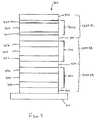
- stacked OLED 100includes substrate 110 , first electrode 120 , second electrode 130 , luminescent region 140 , luminescent region 150 , luminescent region 160 N, intermediate electrode 170 disposed between luminescent region 140 and luminescent region 150 , and intermediate electrode 180 disposed between luminescent region 150 and luminescent region 160 N.
- Nrepresents the number of individual luminescent regions 160 present in the stacked OLED 100 and may be 0, 1 or an integer greater than 1. When N is equal to 0, then a stacked OLED comprises two luminescent regions. Where N is greater than 1, it will be appreciated that intermediate electrodes are disposed between any further successive individual OLEDs.
- the luminescent regions 160 Nmay have the same or different configurations and/or compositions as desired for a particular purpose or intended use.
- Nis taken as 1 in the embodiment of FIG. 1 such that stacked OLED 100 comprises luminescent regions 140 , 150 , and 160 .
- the stacked OLED 100comprises a plurality of individual OLEDs, which are formed a luminescent region disposed between two electrodes.
- stacked OLED 100comprises three individual OLEDs.
- OLED 1 Ais formed from first electrode 120 , luminescent region 140 , and intermediate electrode 170 ;
- OLED 1 Bis formed from intermediate electrode 170 , luminescent region 150 , and intermediate electrode 180 ; and
- individual OLEDsmay share electrodes. More particularly, successive luminescent regions share at least one intermediate electrode.
- Luminescent regions 140 , 150 , and 160each include a first transport zone 142 , 152 , and 162 , respectively, a light emitting layer or zone 144 , 154 , and 164 , respectively, and a second charge transport zone 146 , 156 , and 166 , respectively.
- At least one of the light emitting layers or zones 144 , 154 , or 164is a mixed region comprising a mixture of at least two materials having different electron and hole transport capacities, and optionally a dopant; and wherein the mixed region there is at least one electroluminescent material capable of emitting light.
- the materials having different electron and hole transport capacitiescan be independently selected from hole transport materials, electron transport materials, and bipolar transport material.
- each of the luminescent regions 144 , 154 , and 164comprises a mixed region.
- each of luminescent regions 140 , 150 , and 160depicts each of luminescent regions 140 , 150 , and 160 as having first and second charge transport zones, it will be appreciated that one or more of the charge transport zones may be eliminated depending on the composition of the light emitting layer, intermediate electrodes, and the like.
- a charge transport zonemay be eliminated if the light emitting layer also exhibits a desired charge transporting function (i.e., electron transporting or hole transporting).
- the first electrode 120may be one of a hole injecting anode or an electron injecting cathode.
- the second electrode 130may be one of an electron injecting cathode or a hole injecting anode.
- the first and second electrodesmay be an anode or a cathode as desired for a particular purpose or intended use. For example, in OLED 100 , whether the second electrode 130 is a cathode or an anode depends upon the charge transport function of the layer or zone immediately underlying the second electrode 130 .
- the first charge transport zones 142 , 152 , and 162 , and the second charge transport zones, 146 , 156 , and 166may be one of a hole transport zone or an electron transport zone.
- the nature or function of the first or second charge transport zones of an individual OLED or luminescent region as a hole transport zone or an electron transport zonedepends upon the function of the electrode layer (first electrode, second electrode or intermediate layer) immediately adjacent the respective charge transport zone.
- the composition of makeup of an intermediate electrodeis selected to provide an appropriate charge injecting layer depending on the nature of the layer or zone such as, for example, a charge transport zone immediately adjacent the respective electrode.
- an intermediate electrodemay have to function as a hole injecting layer on one side or surface in contact with a layer having a hole transport function (e.g., a hole transport zone) and also function as an electron injecting layer on the other side or surface in contact with a layer having an electron transport function (e.g., an electron transport zone).
- a hole transport functione.g., a hole transport zone
- an electron injecting layeron the other side or surface in contact with a layer having an electron transport function (e.g., an electron transport zone).
- an intermediate electrodemay be a multi-layered configuration comprising a hole injecting layer and an electron injecting layer adjacent an appropriate layer of a luminescent region.
- the stacked OLEDwhen each of the intermediate electrodes functions as a hole injecting electrode on one side and functions as an electron injecting electrode on the other side, then the stacked OLED can be operated by applying an external forward-bias voltage across the entire stack by means of applying the external forward-bias voltage only across the first and second electrodes; or alternatively by applying an external forward-bias voltage across each individual unit of the stack separately by means of applying external forward-bias voltage across for example, the first electrode and the first intermediate electrode, the first intermediate electrode and the second intermediate electrode, and the second intermediate electrode and the second electrode.
- the stacked OLEDwhen one or more of the intermediate electrodes functions as a hole injecting electrode on both sides or when one or more of the intermediate electrodes functions as an electron injecting electrode on both sides, then the stacked OLED can be operated by applying an external forward-bias voltage across each of the individual units of the stack separately by means of applying external forward-bias voltage across for example, the first electrode and the first intermediate electrode, the first intermediate electrode and the second intermediate electrode, and the second intermediate electrode and the second electrode.
- stacked OLED 100could comprise an anode as the first electrode 120 , a hole transport zone as each of the first charge transport zones 142 , 152 , and 162 , and an electron transport zone as the second charge transport zones 146 , 156 , and 166 .
- intermediate electrodes 170 and 180are multiple layered electrodes with an electron injecting layer adjacent the electron transport zones and a hole injecting layer adjacent the hole transport zones.
- every individual OLED in the stacked configurationincludes an electron transport zone as the second charge transport zone, then the electron transport zone in the last luminescent region (e.g., 160 if N is equal to 1) would be adjacent the second electrode 130 and the second electrode 130 is a cathode.
- the first electrode 120is a cathode
- each of the first charge transport zones 142 , 152 , and 162are each electron transport zones
- each of the second charge transport zones 146 , 156 , and 166are hole transport zones.
- a hole transport zoneis the zone underlying second electrode 130 and second electrode 130 is therefore an anode.
- the intermediate electrodes 170 and 180are multiple layered electrodes with a hole injecting layer adjacent the hole transport zones and an electron injecting layer adjacent the electron transport zones.
- Stacked OLED 200comprises a substrate 210 , an anode 220 an upper electrode 230 , and a plurality of luminescent regions disposed between anode 210 and upper electrode 230 .
- Luminescent region 240is disposed over anode 220 and comprises hole transport zone 242 adjacent anode 220 , light emitting layer or zone 244 , and electron transport zone 246 .
- Intermediate electrode 270is disposed over luminescent region 240 .
- Luminescent region 250is disposed over intermediate electrode 270 and comprises electron transport zone 252 , light emitting layer or zone 254 , and hole transport zone 256 .
- Intermediate electrode 280is disposed over luminescent region 250 .
- Luminescent region 260 Nis disposed over intermediate electrode 280 and comprises charge transport zone 262 , light emitting layer or zone 264 , and second charge transport zone 266 , wherein N is 0, 1, or an integer greater than 1.
- Stacked OLED 200is considered to comprise a plurality of OLEDs, e.g., OLEDs 2 A, 2 B, and 2 C, formed by the respective luminescent regions adjacent an anode, cathode, and/or intermediate electrode.
- the OLED 200may comprise additional or fewer OLEDs depending on the number of luminescent regions incorporated in the stacked OLED configuration.
- a stacked OLED 300comprises a substrate 310 , a cathode 320 , an upper electrode 330 , and a plurality of luminescent regions disposed between the cathode 320 and the upper electrode 330 .
- Luminescent region 340is disposed over cathode 320 .
- Luminescent region 340comprises electron transport zone 342 , light emitting layer or zone 344 , and hole transport zone 346 .
- Intermediate electrode 370is disposed over luminescent region 340 .
- Luminescent region 350is disposed over intermediate electrode 370 and comprises hole transport zone 352 , light emitting layers or zones 354 , and electron transport zone 356 .
- intermediate electrode 370is disposed between hole transport zones 346 and 352 , and therefore comprises a hole injection material.
- Stacked OLED 300may include N number of luminescent regions 360 wherein N is 0, 1, or an integer greater than 1.
- OLED 360comprises a first charge transport zone 362 , luminescent region 364 and a second charge transport zone 366 .
- An intermediate electrode such as intermediate electrode 380is disposed between any successive individual OLEDs.
- Stacked OLED 300comprises a plurality of OLEDs, e.g., OLEDs 3 A, 3 B, and 3 C, formed by the respective luminescent regions adjacent an anode, cathode, and/or intermediate electrode.
- the OLEDmay comprise additional or fewer OLEDs depending on the number of luminescent regions incorporated in the stacked OLED configuration.
- the first charge transport zones of successive luminescent regionshave a charge transport function different from one another and the second charge transport zones of successive luminescent regions have a charge transport function different from one another such that an intermediate electrode is disposed between charge transport zones having the same charge transporting function. That is, in embodiments, the second charge transport layer of one luminescent region has the same charge transporting function as the first charge transport layer of the next successive luminescent region.
- an intermediate electrodecan optionally be a single layer of an appropriate charge injecting material (i.e., hole injecting or electron ejecting). For example, in the embodiment in FIG.
- intermediate electrode 270is disposed between electron transport zones 246 and 252 , and intermediate electrode 270 comprises an electron injecting material. If the pattern continued throughout the stacked OLED, then the upper electrode 230 is determined based on the number of luminescent regions 260 present in the stack: if N is 0 or an even integer, then upper electrode 230 , in this embodiment, is an anode material (intermediate electrode 280 is eliminated if N is equal to 0; if N is equal to 1 or an odd integer, and charge transport layer 262 is a hole transport zone and charge transport zone 266 is an electron transport zone, then upper electrode is a cathode. In the embodiment in FIG.
- intermediate electrode 370is disposed between hole transport zones 246 and 352 and comprises a hole injecting material. If the convention that the first charge transport zones of successive luminescent regions have different functions is carried out throughout the stack, then the function and composition of the upper electrode 330 will depend on the N number of luminescent regions 360 present in the stack, with the upper electrode being a cathode if N is 0 or an even integer and an anode if N is 1 or an odd integer.
- FIGS. 1 , 2 , and 3are merely illustrative examples of possible embodiments of a stacked OLED in accordance with the present disclosure and not intended to limit the scope of a stacked OLED in accordance with the disclosure.
- the overall configuration of a stacked OLED, including the composition and/or function of the individual layersmay be selected as desired for a particular purpose or intended use and are not limited to the specific embodiments described herein.
- At least one luminescent regioncomprises a mixed region.
- a mixed regioncomprises a mixture of at least two materials having different electron and hole transport capacities, and optionally a dopant; and wherein the mixed region there is at least one electroluminescent material capable of emitting light.
- the materials having different electron and hole transport capacitiescan be independently selected from hole transport materials, electron transport materials, and bipolar transport material.
- the mixed regioncomprises two materials having different electron and hole transport capacities, one of which is an electroluminescent material capable of emitting light.
- a mixed regioncomprises two materials having different electron and hole transport capacities optionally one of which is an electroluminescent material, and further comprises an electroluminescent dopant.
- a mixed regioncomprises two materials having different electron and hole transport capacities one of which is an electroluminescent material, and further comprises an electroluminescent dopant, In another embodiment, a mixed region comprises two materials having different electron and hole transport capacities, and further comprises a dopant, and at least one of the two materials or the dopant is an electroluminescent material.
- the emission color of the mixed regionis selected as desired for a particular purpose or intended use.
- the emission color of an individual OLEDis based on the material chosen as the emitter in the mixed region.
- the emission color from the mixed regiondepends on the energy transfer from the materials with the different electron and hole transport capacities to the dopant. For example, if the energy transfer is complete to the dopant, then the emission color from the individual OLED will be the emission color from the dopant. If the energy transfer to the dopant is not complete, then the emission color from the individual OLED is determined by emission colors of the materials with the different electron and hole transport capacities and the dopant.
- the luminescent region of at least one of the individual OLEDs of the stacked OLED configurationcomprises a mixed region.
- the luminescent region of each individual OLEDcomprises a mixed region. It will be appreciated that the number of individual OLEDs which include a mixed region as part of the luminescent region may be selected as desired for a particular purpose or intended use.
- the individual OLEDs of a stacked OLEDmay be made to emit different emission colors. In another embodiment, two or more individual OLEDs may be made to emit the same emission color. In still another embodiment two or more individual OLEDs may be made to emit a first color, two or more individual OLEDs may be made to emit a second color, and so forth. In an even further embodiment, all of the individual OLEDs of a stacked OLED configuration may be made to emit the same emission color to form a monochromatic stacked OLED. In a monochromatic stacked OLED, the luminescent regions of the individual OLEDs may have the same composition, or the luminescent regions may be of different compositions and materials wherein the respective compositions emit the same emission color.
- the substratecan comprise various suitable materials including, for example, polymeric components, glass, quartz and the like.
- suitable polymeric componentsinclude, but are not limited to polyesters, such as MYLAR®, polycarbonates, polyacrylates, polymethacrylates, polysulfones, and the like. Mixtures of these various materials can also be used.
- Other substrate materialscan also be selected provided, for example, that the materials can effectively support the other layers and do not substantially interfere with the device's functional performance.
- the substrateis formed of a light transmission material.
- the thickness of the substrateis not particularly limited except, for example, perhaps by the structural demands of the organic light emitting device and its intended use. Suitable thicknesses include, for example, from at least about 25 ⁇ m to about 10,000 ⁇ m. In embodiments, the substrate has a thickness of from about 100 ⁇ m to about 1,000 ⁇ m. Of course, thicknesses outside of these ranges are possible and within the scope of a stacked OLED in accordance with the present disclosure.
- An anodemay comprise suitable positive hole injecting electrodes, such as indium tin oxide (ITO), tin oxide, gold and platinum.
- ITOindium tin oxide
- Other suitable materials for the anodeinclude, but are not limited to, electrically conductive carbon, ⁇ -conjugated polymers such as polyaniline, polythiophene, polypyrrole, and the like, having, for example, a work function equal to, or greater than, about 4 eV, and preferably from about 4 eV to about 6 eV.
- the anodecan be of any suitable form.
- a thin conductive layermay be coated onto a substrate such as, for example, a transparent or substantially transparent glass plate or plastic film, respectively, or a thin conductive layer may be coated on a hole transport zone.
- Embodiments of a stacked OLED in accordance with the present disclosurecan comprise a light transmissive anode formed from tin oxide or indium tin oxide (ITO) coated on a glass plate.
- ITOindium tin oxide
- very thin light-transparent metallic anodeshaving a thickness, for example, of less than about 200 ⁇ , and in some embodiments from about 75 ⁇ to about 150 ⁇ can be used. These thin anodes can comprise metals such as gold, palladium and the like.
- transparent or semi-transparent thin layers of conductive carbon or conjugated polymerssuch as polyaniline, polythiophene, polypyrrole and the like, having a thickness of, for example, from 50 ⁇ to about 175 ⁇ can be used as anodes.
- conductive carbon or conjugated polymerssuch as polyaniline, polythiophene, polypyrrole and the like, having a thickness of, for example, from 50 ⁇ to about 175 ⁇
- Additional suitable forms of an anodeare disclosed in U.S. Pat. No. 4,885,211, the disclosure of which is incorporated herein by reference in its entirety.
- the thickness of the anodecan range from about 1 nanometer to about 5,000 nanometers. Thicknesses outside of this range can also be used it is believed. The range may depend on the optical constants of the anode material.
- the thickness of the anodeis, in embodiments, from about 30 nanometers to about 300 nanometers.
- the anodecan be formed using any suitable thin film forming method, such as vapor deposition in vacuum, spin-coating, electron-beam deposition and sputtering deposition.
- a hole transport material selected to form the hole transport zones and the mixed region(s)can be any suitable known or later developed material.
- Suitable hole transport materialsinclude, but are not limited to, conductive materials such as polyaniline and its acid-doped forms, polypyrrole, poly(phenylene vinylene), and other suitable semiconductive organic materials. Mixtures of these and other suitable materials can also be used.
- a suitable class of hole transporting materialsare the aromatic tertiary amines such as those disclosed in U.S. Pat. No. 4,539,507, the disclosure of which is totally incorporated herein by reference.
- Suitable exemplary aromatic tertiary aminesinclude, but are not limited to, bis(4-dimethylamino-2-methylphenyl)phenylmethane, N,N,N-tri(p-tolyl)amine, 1,1-bis(4-di-p-tolylaminophenyl)cyclohexane, 1,1-bis(4-di-p-tolylaminophenyl)-4-phenyl cyclohexane, N,N′-diphenyl-N,N′-bis(3-methylphenyl)-1,1′-biphenyl-4,4′-diamine, N,N′-diphenyl-N,N′-bis(3-methylphenyl)-1,1′-biphenyl-4,4′-diamine, N,N′-diphenyl-N,N′-bis(4-methoxyphenyl)-1,1′-biphenyl-4,4′-diamine,
- polynuclear aromatic aminessuitable for the hole transport material
- polynuclear aromatic aminesinclude, but are not limited to, N,N-bis-[4′-(N-phenyl-N-m-tolylamino)-4-biphenylyl]aniline; N,N-bis-[4′-(N-phenyl-N-m-tolylamino)-4-biphenylyl]-m-toluidine; N,N-bis-[4′-(N-phenyl-N-m-tolylamino)-4-biphenylyl]-p-toluidine; N,N-bis-[4′-(N-phenyl-N-p-tolylamino)-4-biphenylyl]aniline; N,N-bis-[4′-(N-phenyl-N-p-tolylamino)-4-biphenylyl]-m-
- a further class of suitable hole transporting materialsare 4,4′-bis(9-carbazolyl)-1,1′-biphenyl compounds.
- Illustrative examples of 4,4′-bis(9-carbazolyl)-1,1′-biphenyl compoundsinclude 4,4′-bis(9-carbazolyl)-1,1′-biphenyl and 4,4′-bis(3-methyl-9-carbazolyl)-1,1′-biphenyl, and the like.
- An exemplary class of the hole transport materialsbeing the indolo-carabazoles, such as, for example, 5,11-di-naphthyl-5,11-dihydroindolo[3,2-b]carbazole and 2,8-dimethyl-5,11-di-naphthyl-5,11-dihydroindolo[3,2-b]carbazole, and others as those described in U.S. Pat. No. 5,942,340, the disclosure of which is totally incorporated herein by reference.
- Suitable materialsinclude N,N,N′N′-tetraarylbenzidines wherein aryl may be selected from phenyl, m-tolyl, p-tolyl, m-methoxyphenyl, p-methoxyphenyl, 1-naphthyl, 2-naphthyl, and the like.
- N,N,N′,N′-tetraarylbenzidinesare N,N′di-naphthyl-N,N′-diphenyl-1,1′-biphenyl-4,4′-diamine, N,N′-bis(3-methylphenyl)-N,N′-diphenyl-1,1′-biphenyl-4,4′-diamine; N,N′-bis(3-methoxyphenyl)-N,N′-diphenyl-1,1′-biphenyl-4,4′-diamine, and the like.
- Still other suitable hole transport materialsalso include the naphthyl-substituted benzidine derivatives.
- a hole transport zonecan further comprise at least one buffer layer (not shown) comprised of a material with certain hole injection and transport properties, and selected such that, for example, device performance is improved.
- Suitable materials that can be utilized in the buffer layerinclude semiconductive organic materials, such as, for example, porphyrin derivatives like 1,10,15,20-tetraphenyl-21H,23H-porphyrin copper (II) disclosed in U.S. Pat. No. 4,356,429, the disclosure of which is totally incorporated herein by reference; copper phthalocyanine, copper tetramethyl phthalocyanine, zinc phthalocyanine, titanium oxide phthalocyanine, magnesium phthalocyanine, and the like. Mixtures of these and other suitable materials can also be used.
- buffer layerexamples include semiconductive and insulative metal compounds, such as for example metal oxides like MgO, Al 2 O 3 , BeO, BaO, AgO, SrO, SiO, SiO 2 , ZrO 2 , CaO, Cs 2 O, Rb 2 O, Li 2 O, K 2 O and Na 2 O; and metal halides like LiF, KCl, NaCl, CsCl, CsF and KF.
- semiconductive and insulative metal compoundssuch as for example metal oxides like MgO, Al 2 O 3 , BeO, BaO, AgO, SrO, SiO, SiO 2 , ZrO 2 , CaO, Cs 2 O, Rb 2 O, Li 2 O, K 2 O and Na 2 O; and metal halides like LiF, KCl, NaCl, CsCl, CsF and KF.
- a hole transport zone optionally including a buffer layercan be prepared by forming, for example, one of the above-described materials into thin films by any suitable known or later developed method. Suitable methods for this purpose include, for example, vapor deposition and spin coating techniques.
- a buffer layercan be located at any position within the hole transport zone. That is, it can be located such that one surface of the buffer layer coincides with one surface of the hole transport zone. In this embodiment the buffer layer is contacting either an anode, intermediate electrode or the mixed region or it can be located such that the two surfaces of the buffer layer are in between two surfaces of a hole transport zone. However, in embodiments a buffer layer is in contact with an anode or hole injecting intermediate cathode.
- a hole transport zonecan have a thickness ranging from about 5 nanometers to about 500 nanometers.
- a buffer layercan have a thickness ranging from about 1 nanometer to about 100 nanometers.
- the thickness of a buffer layeris, for example, at least 1 nanometer less than the thickness of a hole transport zone which comprises a buffer layer.
- the thickness range for a buffer layeris from about 5 nanometers to about 25 nanometers. In other embodiments, the thickness range for a buffer layer is from about 1 nanometer to about 5 nanometers.
- the thickness of a hole transport zone exclusive of the thickness of a buffer layer in the hole transport zonealso has an influence on the performance of the device where, in general, reducing the thickness of the hole transport zone without reducing the thickness of the buffer layer in it can lead to a desirable increase in device stability and, in the same time, to an undesirable decrease in device efficiency.
- a desirable thickness range for a hole transport zone for a particular thickness of the buffer layer in that regionis from about 5 nanometers to about 15 nanometers.
- the thickness range for a hole transport region, exclusive of the thickness of a buffer layeris from about 15 nanometers to about 75 nanometers.
- an individual OLEDcomprise only one of a hole transport zone or an electron transport zone. That is, a light emitting layer or zone, such as a mixed region, may be in direct contact with one of the first electrode, the second electrode, or an intermediate electrode.
- the electron transport material selected to form an electron transport zone or a mixed regioncan be any suitable known or later developed material.
- Suitable electron transport materials that can be used in an electron transport zone and a mixed regioninclude the metal oxinoid compounds, such as the metal chelates of 8-hydroxyquinoline as disclosed in U.S. Pat. Nos. 4,539,507; 5,151,629; 5,150,006 and 5,141,671, the disclosures of each being totally incorporated herein by reference.
- Illustrative examplesinclude tris(8-hydroxyquinolinate)aluminum (AlQ 3 ).
- Another exampleis bis(8-hydroxyquinolato)-(4-phenylphenolato)aluminum (Balq).
- An electron transport zonecan comprise an electron transport material with a thickness ranging, for example, from about 5 nanometers to about 500 nanometers. In embodiments, this thickness is from about 20 nanometers to about 80 nanometers. A thickness outside of these ranges can also be used it is believed. In embodiments such as with the organic light emitting device comprising a multiple-layered electron transport region, the individual layers have a thickness of at least about 1 nanometer.
- a class of bipolar transport materials that can be used in a mixed regioncomprises anthracenes, such as, for example 2-t-butyl-9,10-di-(2-naphthyl) anthracene, 9,10-di-(2-naphthyl)anthracene, 9,10-di-phenyl anthracene, 9,9-bis[4-(9-anthryl)phenyl]fluorine, and 9,9-bis[4-(10-phenyl-9-anthryl)phenyl]fluorine.
- anthracenessuch as, for example 2-t-butyl-9,10-di-(2-naphthyl) anthracene, 9,10-di-(2-naphthyl)anthracene, 9,10-di-phenyl anthracene, 9,9-bis[4-(9-anthryl)phenyl]fluorine, and 9,9-bis[4-(10-phen
- a class of dopant materials that can also be utilized in a mixed regionare the fused ring fluorescent dyes.
- the fused ring fluorescent dyesinclude perylene, rubrene, anthracene, coronene, phenanthrecene, pyrene, and the like, as described in U.S. Pat. No. 3,172,862, the disclosure of which is totally incorporated herein by reference.
- Fluorescent materials that can be used as a dopantinclude butadienes, such as 1,4-diphenylbutadiene and tetraphenyl butadiene, stilbenes, and the like, as described in U.S. Pat. Nos.
- lanthanide metal chelate complexessuch as for example, tris(acetylacetonato)(phenanthroline)terbium, tris(acetyl acetonato)(phenanthroline)europium, and tris(thenoyl trisfluoroacetonato)(phenanthroline)europium, and those disclosed in Kido et al., “White light emitting organic electroluminescent device using lanthanide complexes”, Jpn. J. Appl. Phys., Volume 35, pp. L394-L396 (1996).
- phosphorescent materialssuch as, for example, organometallic compounds containing a heavy metal atom that lead to strong spin-orbit coupling, such as those disclosed in Baldo, et al., “Highly efficient organic phosphorescent emission from organic electroluminescent devices”, Letters to Nature, Volume 395, pp 151-154 (1998).
- phosphorescent materialsinclude 2,3,7,8,12,13,17,18-octaethyl-21H, 23H-phorpine platinum(II) (PtOEP) and fac-tris(2-phenylpyridine)iridium (Ir(ppy) 3 ).
- the mixed regioncomprises a mixture of at least two materials having different electron and hole transport capacities.
- the two materialscan be any two materials that have different hole mobility and/or different electron mobility.
- a materialis considered to be a hole transport material if its hole mobility is at least about 10 times higher than its electron mobility.
- a materialis considered to be an electron transport material if its electron mobility is at least about 10 times higher than its hole mobility.
- a materialis considered to be a bipolar transport material if its hole mobility is equal to its electron mobility, if its hole mobility exceeds its electron mobility by no more than 10 times or if its electron mobility exceeds its hole mobility by no more than 10 times.
- the two materials having different electron and hole transport capacitiescan be independently selected from hole transport materials, electron transport materials and bipolar transport materials, illustrative examples of which have been given above.
- both materialscan be hole transport materials
- both materialscan be electron transport materials
- both materialscan be bipolar transport materials
- one materialcan be a hole transport material and the other material can be an electron transport material
- one materialcan be a hole transport material and the other material can be a bipolar transport material
- one materialcan be an electron transport material and the other material can be a bipolar transport material.
- the two materialsare selected such that the hole mobility of one material is at least two times higher than the hole mobility of the other material.
- the two materialsare selected such that the electron mobility of one material is at least two times higher than the electron mobility of the other material.
- the two materialsare selected such that the hole mobility of one material is at least two times higher than the hole mobility of the other material and/or the electron mobility of one material is at least two times higher than the electron mobility of the other material.
- a mixed regioncan comprise from about 5 volume percent to about 95 volume percent of one of the said two materials, and from about 95 volume percent to about 5 volume percent of the other of the said two materials.
- a mixed regioncan further optionally comprise from about 0.01 volume percent to about 25 volume percent of a dopant material.
- a mixed regioncomprises from about 30 volume percent to about 70 volume percent of one of the said two materials, from about 70 volume percent to about 30 volume percent of the other of the said two materials, and can optionally further comprise from about 0.05 volume percent to about 10 volume percent of a dopant material.
- a mixed regionmay comprise from about 40 volume percent to about 60 volume percent of one of the said two materials, from about 60 volume percent to about 40 volume percent of the other of the said two materials, and optionally from about 0.1 volume percent to about 2 volume percent of a dopant material.
- a dopant material in a mixed regionmay be present in an amount from about 5 volume percent to about 20 volume percent.
- the mixed regions of the individual OLEDsmay be of the same or different compositions with respect to one or both of the materials used to form the mixed region, and the concentration of the materials in the mixed region(s).
- a mixed regioncan be formed by any suitable method that enables the formation of selected mixtures of materials, and optional dopant materials.
- a mixed regioncan be formed by co-evaporating the hole transport material(s), electron transport material(s), and optionally dopant material(s) to form a mixed region.
- the thickness of a mixed regioncan vary from, for example, about 1 nanometer to about 1000 nanometers. In embodiments, the thickness of a mixed region is from about 10 nanometers to about 200 nanometers. In other embodiments, the thickness of a mixed region is from about 20 nanometers to about 100 nanometers. Thicknesses outside of these ranges, however, may also be used. In embodiments wherein a stacked OLED includes two or more individual OLEDs that each comprises a mixed region, the mixed regions may have the same or different thicknesses. The thickness of the respective mixed regions may be selected as desired for a particular purpose or intended use and may allow for tuning the electrical properties of the stacked OLED device.
- a mixed regioncan comprise more than one layer.
- a mixed regioncan selectively be formed to include two, three or even more separate layers.
- the mixing ratios of the two materials having different electron and hole transport capacitiescan be the same in each of the layers, or the mixing ratios can be varied in the layers.
- the multiple layerscan each comprise an equal weight percentage of hole transport material(s) and electron transport material(s).
- the mixed regioncan comprise different amounts of these materials.
- the compositions of the individual layers of a mixed regionmay be the same or different. Adjacent layers having the same material make up are considered different layers if at least one of the respective materials is present in different concentrations.
- Examples of suitable mixed regions for use in a stacked OLED in accordance with the present disclosureinclude, but are not limited to, those disclosed in U.S. Pat. Nos. 6,392,250; 6,392,339; 6,614,175; 6,737,177; 6,753,098; 6,759,146; and 6,773,830, the entire disclosures of which are incorporated herein by reference.
- a cathodecan comprise any suitable metal, including high work function components, having a work function, for example, from about 4 eV to about 6 eV, or low work function components, such as metals with, for example, a work function of from about 2.5 eV to about 4 eV.
- the cathodecan comprise a combination of a low work function (less than about 4 eV) metal and at least one other metal. Effective proportions of the low work function metal to the second or other metal are from less than about 0.1 weight percent to about 99.9 weight percent, and more specifically, from about 3 to about 45 weight percent.
- low work function metalsinclude, but are not limited to, alkaline metals such as lithium or sodium; Group 2A or alkaline earth metals such as beryllium, magnesium, calcium or barium; and Group III metals including rare earth metals and the actinide group metals such as scandium, yttrium, lanthanum, cerium, europium, terbium or actinium. Lithium, magnesium and calcium are preferred low work function metals.
- a cathodecan comprise at least one transparent conducting material, such as for example, indium-tin-oxide (ITO), and other materials, such as, for example, those disclosed in U.S. Pat. Nos. 5,703,436 and 5,707,745, the disclosures of which are totally incorporated herein by reference.
- transparent conducting materialsuch as for example, indium-tin-oxide (ITO)
- ITOindium-tin-oxide
- the thickness of a cathodecan range from, for example, about 10 nanometers to about 500 nanometers, and more specifically, from about 25 to about 300 nanometers, although thicknesses outside of these ranges may be used.
- a cathodecan be formed using any suitable thin film forming method. Exemplary methods for forming the cathode include, but are not limited to, vapor deposition in vacuum, electron-beam deposition, and sputtering deposition.
- a stacked OLEDmay include a thermal protective element (not shown), formed of at least one layer comprising at least one material with certain thermal properties such that the resistance of the stacked OLED to shorting at elevated temperatures is increased.
- a thermal protective element(not shown), formed of at least one layer comprising at least one material with certain thermal properties such that the resistance of the stacked OLED to shorting at elevated temperatures is increased.
- the desired thermal properties of the materials comprising a thermal protective elementare the thermal expansion properties, where certain ranges for these properties are preferred, such as, for example, less than about 9 ⁇ 10 ⁇ 6 (° C. ⁇ 1 ), and preferably, for example, less than about 4 ⁇ 10 ⁇ 6 (° C. 1 ) with no specific lower limits to these properties.
- the rangesare selected based on the thermal properties of the other materials comprising the stacked OLED, especially the thermal properties of the materials comprising the substrate, the hole transport zone and the mixed regions, and the electron transport zones, so that the susceptibility of a stacked OLED to shorting at high temperatures is eliminated, minimized, or substantially reduced.
- the materials utilized in a thermal protective elementcan be selected from any suitable class of materials, such as, for example, organic compounds, inorganic materials, metallic materials, and mixtures thereof. Illustrative examples of materials that can be utilized in the thermal protective element are disclosed in copending application U.S. Ser. No.
- the thickness of a thermal protective elementcan be from about 1 nanometer to about 100 microns, although there may be no upper limit to the thickness except as may be required due to limitations in the fabrication technique or as may be required to avoid detrimental effects on other performance characteristics of the OLED or added costs.
- a suitable thickness range for a thermal protective elementis, for example, from about 10 nanometers to about 1,000 nanometers.
- a thermal protective elementcan be prepared by forming one of the above-described materials into thin films by any suitable known or later developed method. Suitable methods for this purpose include, for example, vapor deposition, sputtering, electron beam, arc evaporation and spin coating techniques. Of these methods, vapor deposition and sputtering are preferred.
- An intermediate electrodemay comprise any suitable hole injecting material or electron injecting material depending on whether an electrode is required to function as a hole injecting contact or an electron injecting contact or both.
- the intermediate electrodesmay be a single layer or a multiple layer electrode.
- the intermediate electrodemay comprise a single layer of a hole injecting material, or a multiple layer configuration wherein the layers adjacent the respective hole transport zones comprises a hole injecting material.
- an intermediate electrodemay be a single layer comprising an electron injecting material, or a multiple layer configuration wherein the layers adjacent the respective electron transport zones comprise an electron injecting material.
- the intermediate electrodeis, in embodiments, a multiple layer electrode with a layer comprising a hole injecting material adjacent the hole transport layer and a layer comprising an electron injecting material adjacent the electron transport layer.
- Suitable materials for the intermediate electrodesincludes ITO, V 2 O 5 , thin layers of Mg:Ag.
- the intermediate electrodemay comprise a metal-organic mixed layer (MOML) such as those described in U.S. Pat. No. 6,841,932 and U.S. patent application Ser. No. 10/401,238, the entire disclosures of which are incorporated herein by reference.
- the intermediate electrodecan be of a configuration as described in copending application Ser. No. 11/133,978, the entire disclosure of which is incorporated herein by reference, in which an MOML is, in some cases, disposed between a hole injecting layer and an electron injecting layer, the hole injecting layer comprising an electron accepting material having a property of oxidizing organic compounds.
- An electron injection layercan comprise at least one material that increases the injection of electrons from a cathode or intermediate electrode into an electron transport zone.
- materials that can be used in the electron injection layerinclude, but are not limited to, metal compounds and suitable organic semiconductive materials.
- Suitable metal compounds that can be utilized in an electron injection layerinclude the alkaline earth metal oxides like SrO, CaO, BaO and others, such as those disclosed in U.S. Pat. Nos. 5,457,565 and 5,739,635, the disclosures of which are totally incorporated herein by reference, and other metal oxides such as Al 2 O 3 , SiO and SiO 2 .
- Other suitable electron injecting materialsinclude metals such as, but not limited to Ca, Li, K, Na, Mg, Al, In, Y, Sr, Cs, Cr, Ba, Sc and compounds thereof.
- a suitable class of metal compounds that can be utilized in an electron injection layerare the alkaline metal halides, such as, for example, LiF, LiCl, NaCl, KF, KCl and others as those disclosed in the above referenced U.S. Pat. No. 5,739,635 and also those disclosed in U.S. Pat. No. 5,776,622, the disclosures of which are totally incorporated herein by reference.
- alkaline metal halidessuch as, for example, LiF, LiCl, NaCl, KF, KCl and others as those disclosed in the above referenced U.S. Pat. No. 5,739,635 and also those disclosed in U.S. Pat. No. 5,776,622, the disclosures of which are totally incorporated herein by reference.
- Suitable organic semiconductive materials that can be used in an electron injection layerinclude materials or components that permit high energy deposition of the cathode. Examples of these materials can be selected from the porphyrin and the naphthacene compounds of which copper phthalocyanine is one example.
- An electron injection layercan further include at least one dopant comprised of an electron injecting dopant, such as for example Li.
- An electron injection layer of an intermediate electrodecan have a thickness ranging, for example, from about 1 nanometer to about 100 nanometers. In embodiments, the thickness range for an electron injection layer is from about 1 nanometer to about 10 nanometers. Another suitable thickness range for an electron injection layer is from about 10 nanometers to about 100 nanometers.
- An electron injection layercan be formed using any suitable thin film forming method, such as vapor deposition in vacuum, electron-beam deposition, and sputtering deposition, wherein the vapor deposition in vacuum is a preferred method.
- Examples of hole injecting materials suitable for an intermediate electrodeinclude those materials previously described herein as suitable as an anode.
- the hole injecting materialcan comprise an electron-accepting material than can oxize an organic compound in a luminescent region.
- Suitable electron-accepting materialsinclude inorganic compounds such as those described in U.S. Pat. No. 6,423,429 to Kido, et al., the entire disclosure of which is incorporated herein by reference.
- Such inorganic compoundsinclude Lewis acids such as FeCl 3 , AICl 3 , GaCl 3 , InCl 3 , SbCl 5 , and combinations thereof.
- Suitable electron-accepting organic materialsincluded, but are not limited to trinitrofluorenone, and 2,3,5,6-tetrafluoro-7,7,8,8-tetrasyanoquinodimethne (F 4 -TCNQ).
- Hole injecting layerscomprising an electron-accepting material as described above may optionally comprise an organic material such as a hole transport material.
- Suitable hole transport materialsinclude those previously described herein including but not limited to, NPB, MTDATA, BP-TPD, CuPc, VOPC, PEDOT, PAN,i and the like. Such hole injecting layers are amenable to vapor deposition techniques.
- Anode configurationscomprising an electron-accepting material and optionally a hole transport material are described in copending applications Ser. No.
- a hole injecting layer of an intermediate electrodecomprises only an electron-accepting material or combination of electron-accepting materials.
- a hole injecting layer of an intermediate electrodecomprises an electron-accepting material or combination of electron-accepting materials and a hole transport material.
- the ratio of electron-accepting material to hole transport material in a hole injecting layer of an intermediate electrodeis from about 10:90 to about 90:10 volume percent.
- a hole injection layer of an intermediate electrodecan have a thickness ranging, for example, from about 1 nanometer to about 100 nanometers.
- the thickness range for a hole injection layeris from about 1 nanometer to about 10nanometers. Another suitable thickness range for a hole injection layer is from about 10 nanometers to about 100 nanometers.
- a hole injection layercan be formed using any suitable thin film forming method, such as vapor deposition in vacuum, electron-beam deposition, and sputtering deposition, wherein the vapor deposition in vacuum is a preferred method.
- a stacked OLEDmay be adjusted or tuned as desired by varying the thickness of any layer of the stacked OLED such as, for example, by changing the thickness of a mixed region, and the like.
- Stacked OLEDs in accordance with the present disclosurewhich include at least one OLED with a mixed region, are further described with reference to the following examples.
- the following examplesare merely illustrative and not intended to be limiting in any manner.
- a first stacked OLED devicewas prepared having a structure as shown in FIG. 4 .
- Stacked OLED 400comprises a substrate 410 , anode 420 , luminescent region 430 , luminescent region 450 , intermediate electrode 440 disposed between luminescent regions 430 and 450 , and cathode 460 .
- Luminescent Regions 430 and 450each include a bottom hole transport zone ( 432 and 452 , respectively), a mixed region ( 434 and 454 , respectively) and an upper electron transport zone ( 436 and 456 , respectively).
- the stacked OLEDwas fabricated using physical vapor deposition in vacuum (5 ⁇ 10 ⁇ 6 Torr) on ITO coated glass substrates, with the ITO serving as the bottom anode.
- the mixed regions 434 and 454had a thickness of 800 angstroms and included N,N′-di(naphthalene-1-yl)-N,N′-diphenyl-benzidine (NPB) as the hole transport material, tris(8-hydroxyquinoline)aluminum (AlQ 3 ) as the electron transport material and (C545T) coumarine dye (10-(2-Benzothiazolyl)-2,3,6,7-tetrahydro-1,1,7,7,-tetramethyl1-1H,5H,11H-[1]benzopyrano[6,7,8-ij]quinolizin-11-one)] green emitting dopant.
- the cathode 460was formed from Mg:Ag.
- the intermediate electrode 440was a multiple layered electrode comprising a metal-organic mixed layer of AlQ 3 /Ag(90:10) having a thickness of 500 angstroms interposed between a layer of LiF having a thickness of 10 angstroms as an electron injecting material layer, and a layer of NPB+10% F 4 -TCNQ having a thickness of 200 angstroms as the hole injecting material layer.
- the devicewas driven using a current density of around 31.25 mA/cm 2 and produced a green emission at a brightness (luminance) of 3910 cd/m 2 .
- the luminance valuetranslates to an electro luminescence efficiency of 12.5 cd/A.
- the CIE color coordinateswere (0.327, 0.617), which amounts to saturated green emission for the device.
- the driving voltage for the devicewas 13.4 V.
- a stacked OLED devicewas prepared that was identical to the device of Example I in all aspects except that the thickness of each of the mixed regions 434 and 454 of the respective luminescent regions 430 and 450 was 400 angstroms instead of 800 angstroms.
- the driving voltagewas only 9.5 V, but the device had an electroluminescence efficiency of 12.4 cd/A, which is comparable to that of the device of Example I.
- the driving voltage of the devicemay be reduced while still maintaining a high electroluminescence efficiency (greater than 10 cd/A).
- An individual OLED devicewas fabricated having a configuration as shown in FIG. 5 .
- the substrate 510 , anode 520 , hole transport zone 532 , mixed region 534 , electron transport zone 536 , and cathode 540had the same composition and thickness of comparable layers in the device of Example I.
- the comparative deviceWhen driven at a current density of around 31.25 mA/cm 2 , the comparative device produced green emission at a brightness of 2600 cd/m 2 .
- the comparative devicehad luminance values that translate to an electroluminescence efficiency of 8.3 cd/A.
- the driving voltage of the comparative devicewas 6.8 V.
- the color coordinates for the comparative examplewere (0.304, 0.621), which amounts to saturated green emission.
Landscapes
- Physics & Mathematics (AREA)
- Nonlinear Science (AREA)
- Optics & Photonics (AREA)
- General Physics & Mathematics (AREA)
- Electroluminescent Light Sources (AREA)
Abstract
Description
Claims (28)
Priority Applications (8)
| Application Number | Priority Date | Filing Date | Title |
|---|---|---|---|
| US11/133,975US7750561B2 (en) | 2005-05-20 | 2005-05-20 | Stacked OLED structure |
| TW095117548ATWI345428B (en) | 2005-05-20 | 2006-05-17 | Stacked oled structure |
| DE102006023511.8ADE102006023511B4 (en) | 2005-05-20 | 2006-05-18 | Stacked OLED structure |
| JP2006138572AJP2006332049A (en) | 2005-05-20 | 2006-05-18 | Multilayer OLED structure |
| CNB200610081017XACN100470827C (en) | 2005-05-20 | 2006-05-19 | Stacked Organic Light Emitting Device Structure |
| FR0604503AFR2886059B1 (en) | 2005-05-20 | 2006-05-19 | STACK ORGANIC ELECTROLUMINESCENT DEVICE AND DISPLAY DEVICE COMPRISING SAME |
| GB0610066AGB2426856B (en) | 2005-05-20 | 2006-05-19 | Stacked oled structure |
| KR1020060045369AKR101328767B1 (en) | 2005-05-20 | 2006-05-19 | Stacked OLED structure |
Applications Claiming Priority (1)
| Application Number | Priority Date | Filing Date | Title |
|---|---|---|---|
| US11/133,975US7750561B2 (en) | 2005-05-20 | 2005-05-20 | Stacked OLED structure |
Publications (2)
| Publication Number | Publication Date |
|---|---|
| US20060261731A1 US20060261731A1 (en) | 2006-11-23 |
| US7750561B2true US7750561B2 (en) | 2010-07-06 |
Family
ID=36660555
Family Applications (1)
| Application Number | Title | Priority Date | Filing Date |
|---|---|---|---|
| US11/133,975Active2027-04-06US7750561B2 (en) | 2005-05-20 | 2005-05-20 | Stacked OLED structure |
Country Status (8)
| Country | Link |
|---|---|
| US (1) | US7750561B2 (en) |
| JP (1) | JP2006332049A (en) |
| KR (1) | KR101328767B1 (en) |
| CN (1) | CN100470827C (en) |
| DE (1) | DE102006023511B4 (en) |
| FR (1) | FR2886059B1 (en) |
| GB (1) | GB2426856B (en) |
| TW (1) | TWI345428B (en) |
Cited By (8)
| Publication number | Priority date | Publication date | Assignee | Title |
|---|---|---|---|---|
| US20120139424A1 (en)* | 2009-09-01 | 2012-06-07 | Koninklijke Philips Electronics N.V. | Illumination device with power source |
| US20130026456A1 (en)* | 2011-07-29 | 2013-01-31 | Kyu-Hwan Hwang | Organic light emitting diode display |
| US20130256723A1 (en)* | 2012-03-30 | 2013-10-03 | Guang hai Jin | Organic light emitting diode display device and method for repairing organic light emitting diode display |
| US20130285027A1 (en)* | 2010-11-09 | 2013-10-31 | Koninklijke Philips Electronics N.V. | Organic electroluminescent device |
| US20220165797A1 (en)* | 2020-11-26 | 2022-05-26 | Stmicroelectronics (Grenoble 2) Sas | Optoelectronic device |
| US12040351B2 (en)* | 2017-11-27 | 2024-07-16 | Seoul Viosys Co., Ltd. | Light emitting diode stack including organic and inorganic layers |
| USRE50440E1 (en) | 2012-12-31 | 2025-05-20 | Lg Display Co., Ltd. | Organic light emitting display device |
| US12433105B2 (en) | 2021-08-06 | 2025-09-30 | Samsung Display Co., Ltd. | Display device |
Families Citing this family (51)
| Publication number | Priority date | Publication date | Assignee | Title |
|---|---|---|---|---|
| US7629695B2 (en)* | 2004-05-20 | 2009-12-08 | Kabushiki Kaisha Toshiba | Stacked electronic component and manufacturing method thereof |
| US7449831B2 (en)* | 2004-08-02 | 2008-11-11 | Lg Display Co., Ltd. | OLEDs having inorganic material containing anode capping layer |
| US7449830B2 (en) | 2004-08-02 | 2008-11-11 | Lg Display Co., Ltd. | OLEDs having improved luminance stability |
| US7777407B2 (en)* | 2005-05-04 | 2010-08-17 | Lg Display Co., Ltd. | Organic light emitting devices comprising a doped triazine electron transport layer |
| US8487527B2 (en) | 2005-05-04 | 2013-07-16 | Lg Display Co., Ltd. | Organic light emitting devices |
| US20060265278A1 (en)* | 2005-05-18 | 2006-11-23 | Napster Llc | System and method for censoring randomly generated character strings |
| US7728517B2 (en) | 2005-05-20 | 2010-06-01 | Lg Display Co., Ltd. | Intermediate electrodes for stacked OLEDs |
| US7795806B2 (en) | 2005-05-20 | 2010-09-14 | Lg Display Co., Ltd. | Reduced reflectance display devices containing a thin-layer metal-organic mixed layer (MOML) |
| US7750561B2 (en) | 2005-05-20 | 2010-07-06 | Lg Display Co., Ltd. | Stacked OLED structure |
| US7943244B2 (en) | 2005-05-20 | 2011-05-17 | Lg Display Co., Ltd. | Display device with metal-organic mixed layer anodes |
| US7811679B2 (en) | 2005-05-20 | 2010-10-12 | Lg Display Co., Ltd. | Display devices with light absorbing metal nanoparticle layers |
| US7531959B2 (en)* | 2005-06-29 | 2009-05-12 | Eastman Kodak Company | White light tandem OLED display with filters |
| US20090267891A1 (en)* | 2008-04-25 | 2009-10-29 | Bamidele Ali | Virtual paper |
| WO2009142030A1 (en)* | 2008-05-19 | 2009-11-26 | シャープ株式会社 | Organic electroluminescent device, display device and illuminating device |
| EP2148370A1 (en) | 2008-07-21 | 2010-01-27 | Technische Universität Braunschweig | Structure of electro-optical devices |
| KR101772662B1 (en)* | 2010-10-22 | 2017-08-30 | 삼성디스플레이 주식회사 | Organic light emitting diode device |
| JP5772085B2 (en)* | 2011-03-09 | 2015-09-02 | セイコーエプソン株式会社 | LIGHT EMITTING ELEMENT, LIGHT EMITTING DEVICE, DISPLAY DEVICE, AND ELECTRONIC DEVICE |
| JP5899635B2 (en)* | 2011-03-23 | 2016-04-06 | 住友化学株式会社 | Organic EL device |
| KR101950836B1 (en)* | 2012-05-22 | 2019-02-22 | 엘지디스플레이 주식회사 | Organic light emitting device and method of fabricating the same |
| GB2505499B (en) | 2012-09-03 | 2017-03-08 | Dst Innovations Ltd | Electroluminescent displays and lighting |
| US9853053B2 (en) | 2012-09-10 | 2017-12-26 | 3B Technologies, Inc. | Three dimension integrated circuits employing thin film transistors |
| KR101941453B1 (en)* | 2012-09-28 | 2019-01-23 | 엘지디스플레이 주식회사 | Organic light emitting display device |
| CN102982742A (en)* | 2012-11-26 | 2013-03-20 | 李崇 | Full-color OLED (Organic Light Emitting Diode) display made by adopting multi-component OLED luminescent device technology and filtering technology |
| KR102040872B1 (en)* | 2012-12-13 | 2019-11-06 | 삼성디스플레이 주식회사 | Organic Light Emitting Diode, Organic Light Emitting Display Device, and method for controlling dual emission of OLED |
| KR102130648B1 (en) | 2012-12-18 | 2020-07-06 | 엘지디스플레이 주식회사 | White organic light emitting device |
| DE102013112602B4 (en)* | 2012-12-18 | 2020-11-12 | Lg Display Co., Ltd. | White organic light emitting device |
| KR102050445B1 (en)* | 2012-12-31 | 2019-11-29 | 엘지디스플레이 주식회사 | Organic light emitting display device |
| CN103296221B (en)* | 2013-06-08 | 2016-07-13 | 广州创维平面显示科技有限公司 | A kind of common electrode laminated organic electroluminescent device |
| KR102081605B1 (en)* | 2013-07-31 | 2020-02-27 | 엘지디스플레이 주식회사 | White organic light emitting diode device |
| KR102141918B1 (en)* | 2013-12-31 | 2020-08-06 | 엘지디스플레이 주식회사 | Organic Light Emitting Display Device |
| KR102165234B1 (en)* | 2014-04-25 | 2020-10-14 | 엘지디스플레이 주식회사 | White organic light emitting device |
| KR102273616B1 (en) | 2014-12-08 | 2021-07-06 | 엘지디스플레이 주식회사 | Organic light emitting device |
| CN104576963A (en)* | 2014-12-18 | 2015-04-29 | 苏州汉克山姆照明科技有限公司 | Organic LED of multilayer structure |
| WO2016099580A2 (en) | 2014-12-23 | 2016-06-23 | Lupino James John | Three dimensional integrated circuits employing thin film transistors |
| WO2016111534A1 (en)* | 2015-01-05 | 2016-07-14 | 코닝정밀소재 주식회사 | Tandem type organic light emitting device |
| JP2016171047A (en)* | 2015-03-16 | 2016-09-23 | パイオニア株式会社 | Light emission device |
| CN105140409A (en)* | 2015-06-26 | 2015-12-09 | 陕西科技大学 | Organic electroluminescent device of parallel structure and preparation method of device |
| DE102015111733A1 (en)* | 2015-07-20 | 2017-01-26 | Osram Oled Gmbh | Organic optoelectronic component and method for producing an organic optoelectronic component |
| JP2017045650A (en)* | 2015-08-27 | 2017-03-02 | 株式会社カネカ | White light-emitting organic el element and white light-emitting organic el panel including the same |
| KR102406606B1 (en)* | 2015-10-08 | 2022-06-09 | 삼성디스플레이 주식회사 | Organic light emitting device, organic light emitting display device having the same and fabricating method of the same |
| KR102389833B1 (en) | 2015-10-23 | 2022-04-21 | 엘지디스플레이 주식회사 | Organic light emitting display device |
| KR102537438B1 (en) | 2015-11-24 | 2023-05-30 | 삼성디스플레이 주식회사 | Compound and Organic light emitting device comprising same |
| KR102552273B1 (en) | 2015-11-26 | 2023-07-07 | 삼성디스플레이 주식회사 | Condensed cyclic compound and organic light emitting device comprising the same |
| KR102546673B1 (en)* | 2015-12-03 | 2023-06-23 | 삼성디스플레이 주식회사 | Organic light emitting device and display device having the same |
| CN106159102A (en)* | 2016-09-28 | 2016-11-23 | Tcl集团股份有限公司 | Lamination QLED device and preparation method thereof |
| CN108134013A (en)* | 2017-12-15 | 2018-06-08 | 昆山维信诺科技有限公司 | Flexible display panels and display device |
| CN109686851A (en)* | 2018-12-26 | 2019-04-26 | 上海晶合光电科技有限公司 | A kind of Organic Light Emitting Diode and preparation method thereof |
| KR102715038B1 (en)* | 2019-07-01 | 2024-10-10 | 삼성전자주식회사 | Luminescent compound, method of manufacturing the same and light emitting device including the same |
| JP2019216290A (en)* | 2019-10-01 | 2019-12-19 | パイオニア株式会社 | Light emission device |
| CN110957347A (en)* | 2019-12-13 | 2020-04-03 | 苏州星烁纳米科技有限公司 | Light-emitting structure, display device and lighting device |
| CN112382652A (en)* | 2020-12-03 | 2021-02-19 | 深圳市极域光学科技有限公司 | Light mixing structure for improving resolution of display device and improving visual acuity |
Citations (129)
| Publication number | Priority date | Publication date | Assignee | Title |
|---|---|---|---|---|
| US2823905A (en) | 1954-12-13 | 1958-02-18 | Tillotson Mfg Co | Charge forming and fuel feeding apparatus |
| US3172862A (en) | 1960-09-29 | 1965-03-09 | Dow Chemical Co | Organic electroluminescent phosphors |
| US3598644A (en) | 1964-10-12 | 1971-08-10 | Xerox Corp | Imaging member fabrication |
| US4084966A (en) | 1968-08-26 | 1978-04-18 | Xerox Corporation | Imaging system using agglomerable migration marking material |
| US4287449A (en) | 1978-02-03 | 1981-09-01 | Sharp Kabushiki Kaisha | Light-absorption film for rear electrodes of electroluminescent display panel |
| US4356429A (en) | 1980-07-17 | 1982-10-26 | Eastman Kodak Company | Organic electroluminescent cell |
| US4539507A (en) | 1983-03-25 | 1985-09-03 | Eastman Kodak Company | Organic electroluminescent devices having improved power conversion efficiencies |
| US4652794A (en) | 1982-12-10 | 1987-03-24 | National Research Development Corporation | Electroluminescent device having a resistive backing layer |
| US4665115A (en) | 1984-08-22 | 1987-05-12 | Exxon Research And Engineering Company | Method for controlling viscosity of organic liquids and compositions |
| US4720432A (en) | 1987-02-11 | 1988-01-19 | Eastman Kodak Company | Electroluminescent device with organic luminescent medium |
| US4769292A (en) | 1987-03-02 | 1988-09-06 | Eastman Kodak Company | Electroluminescent device with modified thin film luminescent zone |
| US4885211A (en) | 1987-02-11 | 1989-12-05 | Eastman Kodak Company | Electroluminescent device with improved cathode |
| US5049780A (en) | 1988-12-02 | 1991-09-17 | National Research Council Of Canada | Optical interference, electroluminescent device having low reflectance |
| US5059861A (en) | 1990-07-26 | 1991-10-22 | Eastman Kodak Company | Organic electroluminescent device with stabilizing cathode capping layer |
| US5141671A (en) | 1991-08-01 | 1992-08-25 | Eastman Kodak Company | Mixed ligand 8-quinolinolato aluminum chelate luminophors |
| US5150006A (en) | 1991-08-01 | 1992-09-22 | Eastman Kodak Company | Blue emitting internal junction organic electroluminescent device (II) |
| US5151629A (en) | 1991-08-01 | 1992-09-29 | Eastman Kodak Company | Blue emitting internal junction organic electroluminescent device (I) |
| US5227252A (en) | 1990-01-22 | 1993-07-13 | Pioneer Electronic Corporation | Electroluminescent device |
| US5247190A (en) | 1989-04-20 | 1993-09-21 | Cambridge Research And Innovation Limited | Electroluminescent devices |
| US5276381A (en) | 1991-09-12 | 1994-01-04 | Pioneer Electronic Corporation | Organic electroluminescent device |
| US5409783A (en) | 1994-02-24 | 1995-04-25 | Eastman Kodak Company | Red-emitting organic electroluminescent device |
| US5429884A (en) | 1992-01-17 | 1995-07-04 | Pioneer Electronic Corporation | Organic electroluminescent element |
| US5457565A (en) | 1992-11-19 | 1995-10-10 | Pioneer Electronic Corporation | Organic electroluminescent device |
| US5516577A (en) | 1992-05-11 | 1996-05-14 | Idemitsu Kosan Co., Ltd. | Organic electroluminescence device |
| US5593788A (en) | 1996-04-25 | 1997-01-14 | Eastman Kodak Company | Organic electroluminescent devices with high operational stability |
| US5601903A (en) | 1993-08-27 | 1997-02-11 | Sanyo Electric Co., Ltd. | Organic electroluminescent elements |
| US5608287A (en) | 1995-02-23 | 1997-03-04 | Eastman Kodak Company | Conductive electron injector for light-emitting diodes |
| US5703436A (en) | 1994-12-13 | 1997-12-30 | The Trustees Of Princeton University | Transparent contacts for organic devices |
| US5707745A (en) | 1994-12-13 | 1998-01-13 | The Trustees Of Princeton University | Multicolor organic light emitting devices |
| US5719467A (en) | 1995-07-27 | 1998-02-17 | Hewlett-Packard Company | Organic electroluminescent device |
| US5728801A (en) | 1996-08-13 | 1998-03-17 | The Dow Chemical Company | Poly (arylamines) and films thereof |
| US5739635A (en) | 1995-04-27 | 1998-04-14 | Pioneer Electric Corporation | Organic electroluminescent device |
| US5776622A (en) | 1996-07-29 | 1998-07-07 | Eastman Kodak Company | Bilayer eletron-injeting electrode for use in an electroluminescent device |
| US5837391A (en)* | 1996-01-17 | 1998-11-17 | Nec Corporation | Organic electroluminescent element having electrode between two fluorescent media for injecting carrier thereinto |
| US5846666A (en) | 1997-02-27 | 1998-12-08 | Xerox Corporation | Electroluminescent devices |
| US5853905A (en) | 1997-09-08 | 1998-12-29 | Motorola, Inc. | Efficient single layer electroluminescent device |
| US5925980A (en) | 1997-05-01 | 1999-07-20 | Motorola, Inc. | Organic electroluminescent device with graded region |
| US5925472A (en) | 1997-03-31 | 1999-07-20 | Xerox Corporation | Electroluminescent devices |
| US5935721A (en) | 1998-03-20 | 1999-08-10 | Eastman Kodak Company | Organic electroluminescent elements for stable electroluminescent |
| US5935720A (en) | 1997-04-07 | 1999-08-10 | Eastman Kodak Company | Red organic electroluminescent devices |
| US5942340A (en) | 1997-10-02 | 1999-08-24 | Xerox Corporation | Indolocarbazole electroluminescent devices |
| US5952115A (en) | 1997-10-02 | 1999-09-14 | Xerox Corporation | Electroluminescent devices |
| US5955836A (en) | 1996-09-21 | 1999-09-21 | U.S. Philips Corporation | Organic electroluminescent component with exciplex formed from a mixed layer of a mixture of hole transporting and electron transporting organic material |
| US5972247A (en) | 1998-03-20 | 1999-10-26 | Eastman Kodak Company | Organic electroluminescent elements for stable blue electroluminescent devices |
| US6013384A (en) | 1997-01-27 | 2000-01-11 | Junji Kido | Organic electroluminescent devices |
| EP0977287A2 (en) | 1998-07-28 | 2000-02-02 | Eastman Kodak Company | Interfacial electron-injecting layer formed from a doped cathode for organic light-emitting structure |
| US6023073A (en) | 1995-11-28 | 2000-02-08 | International Business Machines Corp. | Organic/inorganic alloys used to improve organic electroluminescent devices |
| US6028327A (en) | 1996-11-19 | 2000-02-22 | Nec Corporation | Light-emitting device using an organic thin-film electroluminescent light-emitting element |
| US6057048A (en) | 1998-10-01 | 2000-05-02 | Xerox Corporation | Electroluminescent (EL) devices |
| EP1009044A2 (en) | 1998-12-09 | 2000-06-14 | Eastman Kodak Company | Electroluminescent device with anthracene derivatives hole transport layer |
| US6107734A (en)* | 1998-05-20 | 2000-08-22 | Idemitsu Kosan Co., Ltd. | Organic EL light emitting element with light emitting layers and intermediate conductive layer |
| US6105202A (en) | 1998-01-30 | 2000-08-22 | Stmicrolectronics S.R.L. | Intelligent suction device capable of automatically adapting the suction force according to the conditions of the surface, particularly for vacuum cleaners and the like |
| EP1029832A1 (en) | 1998-08-05 | 2000-08-23 | Nippon Sheet Glass Co., Ltd. | Antireflection colored film coated glass article and plasma display panel optical filter |
| US6130001A (en) | 1997-07-15 | 2000-10-10 | Motorola, Inc. | Organic electroluminescent device with continuous organic medium |
| US6225467B1 (en) | 2000-01-21 | 2001-05-01 | Xerox Corporation | Electroluminescent (EL) devices |
| US6229012B1 (en) | 1998-10-01 | 2001-05-08 | Xerox Corporation | Triazine compositions |
| US6274980B1 (en)* | 1998-11-16 | 2001-08-14 | The Trustees Of Princeton University | Single-color stacked organic light emitting device |
| US6303250B1 (en) | 1999-04-09 | 2001-10-16 | Matsushita Electric Industrial Co., Ltd. | Secondary battery including an electrolytic solution with an organic additive |
| JP2002055203A (en) | 2000-08-11 | 2002-02-20 | Fuji Photo Film Co Ltd | Transparent electrically conductive antireflection film and display using the same |
| US6392339B1 (en) | 1999-07-20 | 2002-05-21 | Xerox Corporation | Organic light emitting devices including mixed region |
| US6392250B1 (en)* | 2000-06-30 | 2002-05-21 | Xerox Corporation | Organic light emitting devices having improved performance |
| US6423429B2 (en) | 1998-03-02 | 2002-07-23 | Junji Kido | Organic electroluminescent devices |
| EP1017118A3 (en) | 1998-12-28 | 2002-07-24 | Sharp Kabushiki Kaisha | Organic electroluminescent element and production method thereof |
| US6437123B1 (en) | 1998-04-30 | 2002-08-20 | Sharp Kabushiki Kaisha | Triazine compounds and their use |
| US20020121860A1 (en) | 2000-12-28 | 2002-09-05 | Satoshi Seo | Light emitting device and method of manufacturing the same |
| US20020135296A1 (en) | 2001-01-26 | 2002-09-26 | Xerox Corporation | Organic light emitting devices |
| US20020145380A1 (en) | 2001-01-26 | 2002-10-10 | Xerox Corporation | Electroluminescent devices |
| US6479172B2 (en) | 2001-01-26 | 2002-11-12 | Xerox Corporation | Electroluminescent (EL) devices |
| US20020180349A1 (en)* | 2001-03-08 | 2002-12-05 | Xerox Corporation | Display devices with organic-metal mixed layer |
| JP2003045676A (en) | 2001-07-26 | 2003-02-14 | Junji Kido | Organic electroluminescent device |
| JP2003086381A (en) | 2001-09-07 | 2003-03-20 | Toray Ind Inc | Light-emitting element |
| US20030071565A1 (en)* | 2001-08-06 | 2003-04-17 | Eastman Kodak Company | Organic light-emitting device having a color-neutral dopant in an emission layer and in a hole-transport layer |
| US6565996B2 (en) | 2001-06-06 | 2003-05-20 | Eastman Kodak Company | Organic light-emitting device having a color-neutral dopant in a hole-transport layer and/or in an electron-transport layer |
| JP2003151777A (en) | 2001-11-08 | 2003-05-23 | Xerox Corp | Organic element |
| US20030116772A1 (en) | 2001-10-30 | 2003-06-26 | Shunpei Yamazaki | Light emitting device |
| EP0977288A3 (en) | 1998-07-28 | 2003-09-10 | Eastman Kodak Company | Electron-injecting layer formed from a dopant layer for organic light-emitting structure |
| US20030189401A1 (en)* | 2002-03-26 | 2003-10-09 | International Manufacturing And Engineering Services Co., Ltd. | Organic electroluminescent device |
| US20030230974A1 (en) | 2002-06-12 | 2003-12-18 | Mei-Ying Chang | [organic light emitting diode display device] |
| US20030234609A1 (en) | 2001-03-08 | 2003-12-25 | Xerox Corporation | Devices with multiple organic-metal mixed layers |
| US20040004433A1 (en) | 2002-06-26 | 2004-01-08 | 3M Innovative Properties Company | Buffer layers for organic electroluminescent devices and methods of manufacture and use |
| US20040009418A1 (en) | 2002-07-02 | 2004-01-15 | Xerox Corporation. | Imaging members |
| US20040018383A1 (en) | 2002-07-26 | 2004-01-29 | Xerox Corporation | Display device with anthracene and triazine derivatives |
| JP2004039617A (en) | 2002-02-15 | 2004-02-05 | Eastman Kodak Co | Stacked organic electroluminescent device |
| US20040027059A1 (en)* | 2002-08-09 | 2004-02-12 | Semiconductor Energy Laboratory Co., Ltd. | Organic electroluminescent device |
| JP2004095546A (en) | 2002-08-09 | 2004-03-25 | Semiconductor Energy Lab Co Ltd | Organic electroluminescent element |
| US6717358B1 (en)* | 2002-10-09 | 2004-04-06 | Eastman Kodak Company | Cascaded organic electroluminescent devices with improved voltage stability |
| US6734625B2 (en) | 2002-07-30 | 2004-05-11 | Xerox Corporation | Organic light emitting device (OLED) with multiple capping layers passivation region on an electrode |
| JP2004139981A (en) | 2002-09-24 | 2004-05-13 | Dainippon Printing Co Ltd | Display element and method of manufacturing the same |
| US6737177B2 (en) | 2001-11-08 | 2004-05-18 | Xerox Corporation | Red organic light emitting devices |
| US6740429B2 (en) | 2001-11-08 | 2004-05-25 | Xerox Corporation | Organic light emitting devices |
| US6750609B2 (en) | 2001-08-22 | 2004-06-15 | Xerox Corporation | OLEDs having light absorbing electrode |
| US6753098B2 (en) | 2001-11-08 | 2004-06-22 | Xerox Corporation | Organic light emitting devices |
| US6773830B2 (en) | 2001-11-08 | 2004-08-10 | Xerox Corporation | Green organic light emitting devices |
| WO2004068911A1 (en) | 2003-01-29 | 2004-08-12 | Semiconductor Energy Laboratory Co., Ltd. | Light-emitting device |
| JP2004317897A (en) | 2003-04-18 | 2004-11-11 | Fuji Photo Film Co Ltd | Colored composition for producing black matrix, photosensitive transfer material, black matrix and its manufacturing method, color filter, liquid crystal display element, and black matrix substrate |
| US20040227460A1 (en) | 2003-05-13 | 2004-11-18 | Eastman Kodak Company | Cascaded organic electroluminescent device having connecting units with N-type and P-type organic layers |
| US6821643B1 (en) | 2000-01-21 | 2004-11-23 | Xerox Corporation | Electroluminescent (EL) devices |
| US20040262615A1 (en) | 2003-06-26 | 2004-12-30 | Eastman Kodak Company | Stacked OLED display having improved efficiency |
| US20050011240A1 (en) | 2003-07-15 | 2005-01-20 | Taiwan Fu Hsing Industrial Co., Ltd. | Door lock |
| JP2005072012A (en) | 2003-08-27 | 2005-03-17 | Novaled Gmbh | Light emitting device and manufacturing method thereof |
| JP2005070574A (en) | 2003-08-27 | 2005-03-17 | Nippon Zeon Co Ltd | Method for producing polymerized toner |
| US20050064235A1 (en) | 2003-09-24 | 2005-03-24 | Eastman Kodak Company | Blue organic electroluminescent devices having a non-hole-blocking layer |
| US20050100760A1 (en) | 2003-10-24 | 2005-05-12 | Pentax Corporation | White organic electroluminescent device |
| US20050112400A1 (en)* | 2002-11-26 | 2005-05-26 | Semiconductor Energy Laboratory Co., Ltd. | Phosphorescence compound and electro field light emitting device having the same |
| US20050140275A1 (en)* | 2003-12-29 | 2005-06-30 | L.G.Philips Lcd Co. Ltd. | Organic electroluminescence device |
| US20050175857A1 (en) | 2004-02-09 | 2005-08-11 | Xerox Corporation | Novel blue emitters for use in organic electroluminescence devices |
| EP1010359B1 (en) | 1997-03-11 | 2006-04-19 | The Ohio State University Research Foundation | Color variable bipolar/ac light-emitting devices |
| EP1160890A3 (en) | 2000-05-24 | 2006-05-03 | Eastman Kodak Company | Reduction of ambient-light-reflection in organic light-emitting devices |
| EP1624504A3 (en) | 2004-08-02 | 2006-05-17 | LG. Philips LCD Co., Ltd. | OLEDs Having Inorganic Material Containing Anode Capping Layer |
| US20060105202A1 (en) | 2004-11-17 | 2006-05-18 | Fuji Photo Film Co., Ltd. | Organic electroluminescent device |
| US20060139516A1 (en) | 2004-12-28 | 2006-06-29 | Seung-Ryull Park | Liquid crystal display device and black matrix for liquid crystal display device |
| JP2006173550A (en) | 2004-02-18 | 2006-06-29 | Sony Corp | Display element |
| US20060139893A1 (en) | 2004-05-20 | 2006-06-29 | Atsushi Yoshimura | Stacked electronic component and manufacturing method thereof |
| US7083490B2 (en) | 2002-06-07 | 2006-08-01 | Philips Lumileds Lighting Company, Llc | Light-emitting devices utilizing nanoparticles |
| JP2006210845A (en) | 2005-01-31 | 2006-08-10 | Sanyo Electric Co Ltd | Organic electroluminescent device and organic electroluminescent display device |
| US20060194076A1 (en) | 2005-02-28 | 2006-08-31 | Fuji Photo Film Co., Ltd. | Organic electroluminescent element |
| US20060251920A1 (en) | 2005-05-04 | 2006-11-09 | Xerox Corporation | Organic light emitting devices comprising a doped triazine electron transport layer |
| US20060251919A1 (en) | 2005-05-04 | 2006-11-09 | Xerox Corporation | Organic light emitting devices |
| US20060263629A1 (en) | 2005-05-20 | 2006-11-23 | Xerox Corporation | Intermediate electrodes for stacked OLEDs |
| US20060263593A1 (en) | 2005-05-20 | 2006-11-23 | Xerox Corporation | Display devices with light absorbing metal nonoparticle layers |
| US20060265278A1 (en) | 2005-05-18 | 2006-11-23 | Napster Llc | System and method for censoring randomly generated character strings |
| US20060261731A1 (en) | 2005-05-20 | 2006-11-23 | Xerox Corporation | Stacked oled structure |
| US20060261727A1 (en) | 2005-05-20 | 2006-11-23 | Xerox Corporation | Reduced reflectance display devices containing a thin-layer metal-organic mixed layer (MOML) |
| US20060263628A1 (en) | 2005-05-20 | 2006-11-23 | Xerox Corporation | Display device with metal-organic mixed layer anodes |
| EP1167488B1 (en) | 1999-09-21 | 2007-04-25 | Idemitsu Kosan Company Limited | Organic electroluminescent device and organic luminous medium |
| US7211948B2 (en) | 2004-01-13 | 2007-05-01 | Eastman Kodak Company | Using a crystallization-inhibitor in organic electroluminescent devices |
| US7291404B2 (en) | 2003-04-17 | 2007-11-06 | Lg.Philips Lcd Co., Ltd. | Organic light emitting devices |
| EP1624503A3 (en) | 2004-08-02 | 2007-11-14 | LG. Philips LCD Co., Ltd. | OLEDs having improved luminance stability |
| US7351999B2 (en)* | 2004-12-16 | 2008-04-01 | Au Optronics Corporation | Organic light-emitting device with improved layer structure |
Family Cites Families (7)
| Publication number | Priority date | Publication date | Assignee | Title |
|---|---|---|---|---|
| JPH11312584A (en)* | 1998-04-28 | 1999-11-09 | Tdk Corp | Organic el element |
| JP3875401B2 (en)* | 1998-05-12 | 2007-01-31 | Tdk株式会社 | Organic EL display device and organic EL element |
| TW593622B (en)* | 2000-05-19 | 2004-06-21 | Eastman Kodak Co | Method of using predoped materials for making an organic light-emitting device |
| JP2003282267A (en)* | 2002-03-22 | 2003-10-03 | Matsushita Electric Works Ltd | Light emitting device |
| JP2005123205A (en)* | 2002-10-24 | 2005-05-12 | Toyota Industries Corp | Organic el element |
| JP3970253B2 (en)* | 2003-03-27 | 2007-09-05 | 三洋電機株式会社 | Organic electroluminescence device |
| JP4899284B2 (en)* | 2003-07-18 | 2012-03-21 | コニカミノルタホールディングス株式会社 | Organic electroluminescence element, lighting device and display device |
- 2005
- 2005-05-20USUS11/133,975patent/US7750561B2/enactiveActive
- 2006
- 2006-05-17TWTW095117548Apatent/TWI345428B/enactive
- 2006-05-18DEDE102006023511.8Apatent/DE102006023511B4/enactiveActive
- 2006-05-18JPJP2006138572Apatent/JP2006332049A/enactivePending
- 2006-05-19FRFR0604503Apatent/FR2886059B1/enactiveActive
- 2006-05-19CNCNB200610081017XApatent/CN100470827C/enactiveActive
- 2006-05-19KRKR1020060045369Apatent/KR101328767B1/enactiveActive
- 2006-05-19GBGB0610066Apatent/GB2426856B/enactiveActive
Patent Citations (139)
| Publication number | Priority date | Publication date | Assignee | Title |
|---|---|---|---|---|
| US2823905A (en) | 1954-12-13 | 1958-02-18 | Tillotson Mfg Co | Charge forming and fuel feeding apparatus |
| US3172862A (en) | 1960-09-29 | 1965-03-09 | Dow Chemical Co | Organic electroluminescent phosphors |
| US3598644A (en) | 1964-10-12 | 1971-08-10 | Xerox Corp | Imaging member fabrication |
| US4084966A (en) | 1968-08-26 | 1978-04-18 | Xerox Corporation | Imaging system using agglomerable migration marking material |
| US4287449A (en) | 1978-02-03 | 1981-09-01 | Sharp Kabushiki Kaisha | Light-absorption film for rear electrodes of electroluminescent display panel |
| US4356429A (en) | 1980-07-17 | 1982-10-26 | Eastman Kodak Company | Organic electroluminescent cell |
| US4652794A (en) | 1982-12-10 | 1987-03-24 | National Research Development Corporation | Electroluminescent device having a resistive backing layer |
| US4539507A (en) | 1983-03-25 | 1985-09-03 | Eastman Kodak Company | Organic electroluminescent devices having improved power conversion efficiencies |
| US4665115A (en) | 1984-08-22 | 1987-05-12 | Exxon Research And Engineering Company | Method for controlling viscosity of organic liquids and compositions |
| US4720432A (en) | 1987-02-11 | 1988-01-19 | Eastman Kodak Company | Electroluminescent device with organic luminescent medium |
| US4885211A (en) | 1987-02-11 | 1989-12-05 | Eastman Kodak Company | Electroluminescent device with improved cathode |
| US4769292A (en) | 1987-03-02 | 1988-09-06 | Eastman Kodak Company | Electroluminescent device with modified thin film luminescent zone |
| US5049780A (en) | 1988-12-02 | 1991-09-17 | National Research Council Of Canada | Optical interference, electroluminescent device having low reflectance |
| US5247190A (en) | 1989-04-20 | 1993-09-21 | Cambridge Research And Innovation Limited | Electroluminescent devices |
| US5227252A (en) | 1990-01-22 | 1993-07-13 | Pioneer Electronic Corporation | Electroluminescent device |
| US5059861A (en) | 1990-07-26 | 1991-10-22 | Eastman Kodak Company | Organic electroluminescent device with stabilizing cathode capping layer |
| US5150006A (en) | 1991-08-01 | 1992-09-22 | Eastman Kodak Company | Blue emitting internal junction organic electroluminescent device (II) |
| US5151629A (en) | 1991-08-01 | 1992-09-29 | Eastman Kodak Company | Blue emitting internal junction organic electroluminescent device (I) |
| US5141671A (en) | 1991-08-01 | 1992-08-25 | Eastman Kodak Company | Mixed ligand 8-quinolinolato aluminum chelate luminophors |
| US5276381A (en) | 1991-09-12 | 1994-01-04 | Pioneer Electronic Corporation | Organic electroluminescent device |
| US5429884A (en) | 1992-01-17 | 1995-07-04 | Pioneer Electronic Corporation | Organic electroluminescent element |
| US5516577A (en) | 1992-05-11 | 1996-05-14 | Idemitsu Kosan Co., Ltd. | Organic electroluminescence device |
| US5457565A (en) | 1992-11-19 | 1995-10-10 | Pioneer Electronic Corporation | Organic electroluminescent device |
| US5601903A (en) | 1993-08-27 | 1997-02-11 | Sanyo Electric Co., Ltd. | Organic electroluminescent elements |
| US5409783A (en) | 1994-02-24 | 1995-04-25 | Eastman Kodak Company | Red-emitting organic electroluminescent device |
| US5703436A (en) | 1994-12-13 | 1997-12-30 | The Trustees Of Princeton University | Transparent contacts for organic devices |
| US5707745A (en) | 1994-12-13 | 1998-01-13 | The Trustees Of Princeton University | Multicolor organic light emitting devices |
| US5608287A (en) | 1995-02-23 | 1997-03-04 | Eastman Kodak Company | Conductive electron injector for light-emitting diodes |
| US5739635A (en) | 1995-04-27 | 1998-04-14 | Pioneer Electric Corporation | Organic electroluminescent device |
| US5719467A (en) | 1995-07-27 | 1998-02-17 | Hewlett-Packard Company | Organic electroluminescent device |
| US6023073A (en) | 1995-11-28 | 2000-02-08 | International Business Machines Corp. | Organic/inorganic alloys used to improve organic electroluminescent devices |
| US5837391A (en)* | 1996-01-17 | 1998-11-17 | Nec Corporation | Organic electroluminescent element having electrode between two fluorescent media for injecting carrier thereinto |
| US5593788A (en) | 1996-04-25 | 1997-01-14 | Eastman Kodak Company | Organic electroluminescent devices with high operational stability |
| US5776622A (en) | 1996-07-29 | 1998-07-07 | Eastman Kodak Company | Bilayer eletron-injeting electrode for use in an electroluminescent device |
| US5728801A (en) | 1996-08-13 | 1998-03-17 | The Dow Chemical Company | Poly (arylamines) and films thereof |
| US5955836A (en) | 1996-09-21 | 1999-09-21 | U.S. Philips Corporation | Organic electroluminescent component with exciplex formed from a mixed layer of a mixture of hole transporting and electron transporting organic material |
| US6028327A (en) | 1996-11-19 | 2000-02-22 | Nec Corporation | Light-emitting device using an organic thin-film electroluminescent light-emitting element |
| US6013384A (en) | 1997-01-27 | 2000-01-11 | Junji Kido | Organic electroluminescent devices |
| US5846666A (en) | 1997-02-27 | 1998-12-08 | Xerox Corporation | Electroluminescent devices |
| EP1010359B1 (en) | 1997-03-11 | 2006-04-19 | The Ohio State University Research Foundation | Color variable bipolar/ac light-emitting devices |
| US5925472A (en) | 1997-03-31 | 1999-07-20 | Xerox Corporation | Electroluminescent devices |
| US5935720A (en) | 1997-04-07 | 1999-08-10 | Eastman Kodak Company | Red organic electroluminescent devices |
| US5925980A (en) | 1997-05-01 | 1999-07-20 | Motorola, Inc. | Organic electroluminescent device with graded region |
| US6130001A (en) | 1997-07-15 | 2000-10-10 | Motorola, Inc. | Organic electroluminescent device with continuous organic medium |
| US5853905A (en) | 1997-09-08 | 1998-12-29 | Motorola, Inc. | Efficient single layer electroluminescent device |
| US5942340A (en) | 1997-10-02 | 1999-08-24 | Xerox Corporation | Indolocarbazole electroluminescent devices |
| US5952115A (en) | 1997-10-02 | 1999-09-14 | Xerox Corporation | Electroluminescent devices |
| US6105202A (en) | 1998-01-30 | 2000-08-22 | Stmicrolectronics S.R.L. | Intelligent suction device capable of automatically adapting the suction force according to the conditions of the surface, particularly for vacuum cleaners and the like |
| US6423429B2 (en) | 1998-03-02 | 2002-07-23 | Junji Kido | Organic electroluminescent devices |
| US5935721A (en) | 1998-03-20 | 1999-08-10 | Eastman Kodak Company | Organic electroluminescent elements for stable electroluminescent |
| US5972247A (en) | 1998-03-20 | 1999-10-26 | Eastman Kodak Company | Organic electroluminescent elements for stable blue electroluminescent devices |
| US6437123B1 (en) | 1998-04-30 | 2002-08-20 | Sharp Kabushiki Kaisha | Triazine compounds and their use |
| US6107734A (en)* | 1998-05-20 | 2000-08-22 | Idemitsu Kosan Co., Ltd. | Organic EL light emitting element with light emitting layers and intermediate conductive layer |
| EP0977288A3 (en) | 1998-07-28 | 2003-09-10 | Eastman Kodak Company | Electron-injecting layer formed from a dopant layer for organic light-emitting structure |
| EP0977287A2 (en) | 1998-07-28 | 2000-02-02 | Eastman Kodak Company | Interfacial electron-injecting layer formed from a doped cathode for organic light-emitting structure |
| EP1029832A1 (en) | 1998-08-05 | 2000-08-23 | Nippon Sheet Glass Co., Ltd. | Antireflection colored film coated glass article and plasma display panel optical filter |
| US6229012B1 (en) | 1998-10-01 | 2001-05-08 | Xerox Corporation | Triazine compositions |
| US6057048A (en) | 1998-10-01 | 2000-05-02 | Xerox Corporation | Electroluminescent (EL) devices |
| US6274980B1 (en)* | 1998-11-16 | 2001-08-14 | The Trustees Of Princeton University | Single-color stacked organic light emitting device |
| EP1009044A2 (en) | 1998-12-09 | 2000-06-14 | Eastman Kodak Company | Electroluminescent device with anthracene derivatives hole transport layer |
| US6465115B2 (en) | 1998-12-09 | 2002-10-15 | Eastman Kodak Company | Electroluminescent device with anthracene derivatives hole transport layer |
| EP1017118A3 (en) | 1998-12-28 | 2002-07-24 | Sharp Kabushiki Kaisha | Organic electroluminescent element and production method thereof |
| US6303250B1 (en) | 1999-04-09 | 2001-10-16 | Matsushita Electric Industrial Co., Ltd. | Secondary battery including an electrolytic solution with an organic additive |
| US6392339B1 (en) | 1999-07-20 | 2002-05-21 | Xerox Corporation | Organic light emitting devices including mixed region |
| EP1167488B1 (en) | 1999-09-21 | 2007-04-25 | Idemitsu Kosan Company Limited | Organic electroluminescent device and organic luminous medium |
| US6821643B1 (en) | 2000-01-21 | 2004-11-23 | Xerox Corporation | Electroluminescent (EL) devices |
| US6225467B1 (en) | 2000-01-21 | 2001-05-01 | Xerox Corporation | Electroluminescent (EL) devices |
| EP1160890A3 (en) | 2000-05-24 | 2006-05-03 | Eastman Kodak Company | Reduction of ambient-light-reflection in organic light-emitting devices |
| US6392250B1 (en)* | 2000-06-30 | 2002-05-21 | Xerox Corporation | Organic light emitting devices having improved performance |
| JP2002055203A (en) | 2000-08-11 | 2002-02-20 | Fuji Photo Film Co Ltd | Transparent electrically conductive antireflection film and display using the same |
| US20020121860A1 (en) | 2000-12-28 | 2002-09-05 | Satoshi Seo | Light emitting device and method of manufacturing the same |
| US6479172B2 (en) | 2001-01-26 | 2002-11-12 | Xerox Corporation | Electroluminescent (EL) devices |
| US6562485B2 (en) | 2001-01-26 | 2003-05-13 | Xerox Corporation | Electroluminescent (EL) devices |
| US20020145380A1 (en) | 2001-01-26 | 2002-10-10 | Xerox Corporation | Electroluminescent devices |
| US20020135296A1 (en) | 2001-01-26 | 2002-09-26 | Xerox Corporation | Organic light emitting devices |
| US6614175B2 (en) | 2001-01-26 | 2003-09-02 | Xerox Corporation | Organic light emitting devices |
| US6765348B2 (en) | 2001-01-26 | 2004-07-20 | Xerox Corporation | Electroluminescent devices containing thermal protective layers |
| US20030234609A1 (en) | 2001-03-08 | 2003-12-25 | Xerox Corporation | Devices with multiple organic-metal mixed layers |
| US7288887B2 (en) | 2001-03-08 | 2007-10-30 | Lg.Philips Lcd Co. Ltd. | Devices with multiple organic-metal mixed layers |
| US6841932B2 (en) | 2001-03-08 | 2005-01-11 | Xerox Corporation | Display devices with organic-metal mixed layer |
| US20020180349A1 (en)* | 2001-03-08 | 2002-12-05 | Xerox Corporation | Display devices with organic-metal mixed layer |
| US6565996B2 (en) | 2001-06-06 | 2003-05-20 | Eastman Kodak Company | Organic light-emitting device having a color-neutral dopant in a hole-transport layer and/or in an electron-transport layer |
| JP2003045676A (en) | 2001-07-26 | 2003-02-14 | Junji Kido | Organic electroluminescent device |
| US20030071565A1 (en)* | 2001-08-06 | 2003-04-17 | Eastman Kodak Company | Organic light-emitting device having a color-neutral dopant in an emission layer and in a hole-transport layer |
| US6750609B2 (en) | 2001-08-22 | 2004-06-15 | Xerox Corporation | OLEDs having light absorbing electrode |
| JP2003086381A (en) | 2001-09-07 | 2003-03-20 | Toray Ind Inc | Light-emitting element |
| US20030116772A1 (en) | 2001-10-30 | 2003-06-26 | Shunpei Yamazaki | Light emitting device |
| US6737177B2 (en) | 2001-11-08 | 2004-05-18 | Xerox Corporation | Red organic light emitting devices |
| US20030134146A1 (en) | 2001-11-08 | 2003-07-17 | Xerox Corporation | Organic devices |
| EP1311139B1 (en) | 2001-11-08 | 2008-01-02 | LG. Philips LCD Co., Ltd. | Green organic light emitting devices |
| US6773830B2 (en) | 2001-11-08 | 2004-08-10 | Xerox Corporation | Green organic light emitting devices |
| US6740429B2 (en) | 2001-11-08 | 2004-05-25 | Xerox Corporation | Organic light emitting devices |
| JP2003151777A (en) | 2001-11-08 | 2003-05-23 | Xerox Corp | Organic element |
| US6753098B2 (en) | 2001-11-08 | 2004-06-22 | Xerox Corporation | Organic light emitting devices |
| US6759146B2 (en) | 2001-11-08 | 2004-07-06 | Xerox Corporation | Organic devices |
| JP2004039617A (en) | 2002-02-15 | 2004-02-05 | Eastman Kodak Co | Stacked organic electroluminescent device |
| US20030189401A1 (en)* | 2002-03-26 | 2003-10-09 | International Manufacturing And Engineering Services Co., Ltd. | Organic electroluminescent device |
| US7083490B2 (en) | 2002-06-07 | 2006-08-01 | Philips Lumileds Lighting Company, Llc | Light-emitting devices utilizing nanoparticles |
| US20030230974A1 (en) | 2002-06-12 | 2003-12-18 | Mei-Ying Chang | [organic light emitting diode display device] |
| US20040004433A1 (en) | 2002-06-26 | 2004-01-08 | 3M Innovative Properties Company | Buffer layers for organic electroluminescent devices and methods of manufacture and use |
| US20040009418A1 (en) | 2002-07-02 | 2004-01-15 | Xerox Corporation. | Imaging members |
| US20040018383A1 (en) | 2002-07-26 | 2004-01-29 | Xerox Corporation | Display device with anthracene and triazine derivatives |
| US6734625B2 (en) | 2002-07-30 | 2004-05-11 | Xerox Corporation | Organic light emitting device (OLED) with multiple capping layers passivation region on an electrode |
| US20040027059A1 (en)* | 2002-08-09 | 2004-02-12 | Semiconductor Energy Laboratory Co., Ltd. | Organic electroluminescent device |
| JP2004095546A (en) | 2002-08-09 | 2004-03-25 | Semiconductor Energy Lab Co Ltd | Organic electroluminescent element |
| JP2004139981A (en) | 2002-09-24 | 2004-05-13 | Dainippon Printing Co Ltd | Display element and method of manufacturing the same |
| US6717358B1 (en)* | 2002-10-09 | 2004-04-06 | Eastman Kodak Company | Cascaded organic electroluminescent devices with improved voltage stability |
| EP1408563A3 (en) | 2002-10-09 | 2006-10-04 | Eastman Kodak Company | Cascaded organic electroluminescent devices with improved voltage stability |
| US20050112400A1 (en)* | 2002-11-26 | 2005-05-26 | Semiconductor Energy Laboratory Co., Ltd. | Phosphorescence compound and electro field light emitting device having the same |
| WO2004068911A1 (en) | 2003-01-29 | 2004-08-12 | Semiconductor Energy Laboratory Co., Ltd. | Light-emitting device |
| US7291404B2 (en) | 2003-04-17 | 2007-11-06 | Lg.Philips Lcd Co., Ltd. | Organic light emitting devices |
| JP2004317897A (en) | 2003-04-18 | 2004-11-11 | Fuji Photo Film Co Ltd | Colored composition for producing black matrix, photosensitive transfer material, black matrix and its manufacturing method, color filter, liquid crystal display element, and black matrix substrate |
| US20040227460A1 (en) | 2003-05-13 | 2004-11-18 | Eastman Kodak Company | Cascaded organic electroluminescent device having connecting units with N-type and P-type organic layers |
| US20040262615A1 (en) | 2003-06-26 | 2004-12-30 | Eastman Kodak Company | Stacked OLED display having improved efficiency |
| US20050011240A1 (en) | 2003-07-15 | 2005-01-20 | Taiwan Fu Hsing Industrial Co., Ltd. | Door lock |
| JP2005072012A (en) | 2003-08-27 | 2005-03-17 | Novaled Gmbh | Light emitting device and manufacturing method thereof |
| JP2005070574A (en) | 2003-08-27 | 2005-03-17 | Nippon Zeon Co Ltd | Method for producing polymerized toner |
| US20050064235A1 (en) | 2003-09-24 | 2005-03-24 | Eastman Kodak Company | Blue organic electroluminescent devices having a non-hole-blocking layer |
| US20050100760A1 (en) | 2003-10-24 | 2005-05-12 | Pentax Corporation | White organic electroluminescent device |
| US20050140275A1 (en)* | 2003-12-29 | 2005-06-30 | L.G.Philips Lcd Co. Ltd. | Organic electroluminescence device |
| US7211948B2 (en) | 2004-01-13 | 2007-05-01 | Eastman Kodak Company | Using a crystallization-inhibitor in organic electroluminescent devices |
| US20050175857A1 (en) | 2004-02-09 | 2005-08-11 | Xerox Corporation | Novel blue emitters for use in organic electroluminescence devices |
| JP2006173550A (en) | 2004-02-18 | 2006-06-29 | Sony Corp | Display element |
| US20060139893A1 (en) | 2004-05-20 | 2006-06-29 | Atsushi Yoshimura | Stacked electronic component and manufacturing method thereof |
| EP1624504A3 (en) | 2004-08-02 | 2006-05-17 | LG. Philips LCD Co., Ltd. | OLEDs Having Inorganic Material Containing Anode Capping Layer |
| EP1624503A3 (en) | 2004-08-02 | 2007-11-14 | LG. Philips LCD Co., Ltd. | OLEDs having improved luminance stability |
| US20060105202A1 (en) | 2004-11-17 | 2006-05-18 | Fuji Photo Film Co., Ltd. | Organic electroluminescent device |
| US7351999B2 (en)* | 2004-12-16 | 2008-04-01 | Au Optronics Corporation | Organic light-emitting device with improved layer structure |
| US20060139516A1 (en) | 2004-12-28 | 2006-06-29 | Seung-Ryull Park | Liquid crystal display device and black matrix for liquid crystal display device |
| JP2006210845A (en) | 2005-01-31 | 2006-08-10 | Sanyo Electric Co Ltd | Organic electroluminescent device and organic electroluminescent display device |
| US20060194076A1 (en) | 2005-02-28 | 2006-08-31 | Fuji Photo Film Co., Ltd. | Organic electroluminescent element |
| US20060251920A1 (en) | 2005-05-04 | 2006-11-09 | Xerox Corporation | Organic light emitting devices comprising a doped triazine electron transport layer |
| US20060251919A1 (en) | 2005-05-04 | 2006-11-09 | Xerox Corporation | Organic light emitting devices |
| US20060265278A1 (en) | 2005-05-18 | 2006-11-23 | Napster Llc | System and method for censoring randomly generated character strings |
| US20060263628A1 (en) | 2005-05-20 | 2006-11-23 | Xerox Corporation | Display device with metal-organic mixed layer anodes |
| US20060261727A1 (en) | 2005-05-20 | 2006-11-23 | Xerox Corporation | Reduced reflectance display devices containing a thin-layer metal-organic mixed layer (MOML) |
| US20060261731A1 (en) | 2005-05-20 | 2006-11-23 | Xerox Corporation | Stacked oled structure |
| US20060263593A1 (en) | 2005-05-20 | 2006-11-23 | Xerox Corporation | Display devices with light absorbing metal nonoparticle layers |
| US20060263629A1 (en) | 2005-05-20 | 2006-11-23 | Xerox Corporation | Intermediate electrodes for stacked OLEDs |
Non-Patent Citations (33)
| Title |
|---|
| A. Gyoutoku et al., "An Organic Electroluminescent Dot-Matrix Display Using Carbon Underlayer", Synthetic Metals, vol. 91, pp. 73-75 (1997). |
| Aziz et al., "Reduced reflectance cathode for organic light-emitting devices using metal organic mixtures", Applied Physics Letters, vol. 83, No. 1, pp. 186-188 (2003). |
| Baldo et al., "Highly efficient phosphorescent emission from organic electroluminescent devices," Letters to Nature, vol. 395, pp. 151-154 (1998). |
| Bernius et al., "Developmental Progress of Electroluminescent Polymeric Materials and Devices" Proceedings of SPIE Conference on Organic Light Emitting Materials and Devices III, Denver, Colo., vol. 3797, p. 129-137 (Jul. 1999). |
| Blochwitz et al., "Non-polymeric OLEDs with a doped amorphous hole transport layer and operating voltages down to 3.2 V to achieve 100 cd/m2", Synth. Metals 2002, vol. 127, pp. 169-173. |
| Carter et al., "Polymeric anodes for improved polymer light-emitting diode performance", Appl. Phys. Lett. 70 (16), pp. 2067-2069 (Apr. 21, 1997). |
| Chengfeng Qiu et al., "Praseodymium Oxide Coated Anode for Organic Light-Emitting Diode", Applied Physics Letters, vol. 80, No. 19, pp. 3485-3487 (May 13, 2002). |
| Chengfeng Qiu et al., Comparative Study of Metal or Oxide Capped Indium-Tin Oxide Anodes for Organic Light-Emitting Diodes, Journal of Applied Physics, vol. 93, No. 6 pp. 3253-3257 (Mar. 15, 2003). |
| Chieh-Wei Chen et al., "Top-Emitting Organic Light-Emitting Devices Using Surface-Modified Ag Anode," Applied Physics Letters, vol. 83, No. 25, pp. 5127-5129 (Dec. 22, 2003). |
| Choong et al, Organic light-emitting diodes with a bipolar transport layer, Applied Physics Letters, vol. 75, No. 2, Jul. 12, 1999, p[s. 172-174.* |
| Choong et al., Organic light-emitting diodes with a bipolar transport lay r , Applied Physics Letters, vol. 75, No. 2, 1999, pp. 172-174. |
| Day et al., "The use of charge transfer interlayers to control hole injection in molecular organic light emitting diodes", Thin Solid Films, vol. 410, pp. 159-166 (Mar. 2002). |
| Endo et al., "Organic Electroluminescent Devices with a Vacuum-Deposited Lewis-Acid-Doped Hole-Injecting Layer", Japanese Journal of Applied Physics, vol. 41, No. 3B, 2002, pp. L358-L360. |
| Endo et al., "Organic Electroluminescent Devices with a Vacuum-Deposited Lewis-Acid-Doped Hole-Injecting Layer", Japanese Journal of Applied Physics, vol. 41, pp. L358-L360 (Mar. 2002). |
| H. Michelle Grandia et al.; Light-Absorption Phenomena in Novel Low-Reflective Cathodes for Organic Light-Emitting Devices Utilizing Metal-Organic Mixtures; Advanced Materials, 2003, 15, No. 23; pp. 3021-3024. |
| Hongjin Jiang et al., "Improvement of Organic Light-Emitting Diodes Performance by the Insertion of a Si3N4 Layer", Thin Solid Films, vol. 363, pp. 25-29 (2000). |
| Hyun-Ouk Ha et al., "Improving the efficiency of organic electroluminescent devices by introducing an electron-accepting and thermally stable polymer", Optical Materials, vol. 21 pp. 165-168 (2002). |
| I-Min Chan et al., "Enhanced Hole Injections in Organic Light-Emitting Devices by Depositing Nickel Oxide on Indium Tin Oxide Anode," Applied Physics Letters, vol. 81, No. 10, pp. 1899-1901 (Sep. 2, 2002). |
| Kido et al., "White-Light-Emitting Organic Electroluminescent Device Using Lanthanide Complexes," Jpn. J. Appl. Phys., vol. 35, pp. L394-L396 (1996). |
| Kim et al., "Anode material based on Zr-doped ZnO thin films for organic light-emitting diodes", Appl. Phys. Lett., vol. 83, No. 18, 2003, pp. 3809-3811. |
| Kim et al., "Molecular organic light-emitting diodes using highly conducting polymers as anodes", Appl. Phys. Lett., vol. 80 No. 20, pp. 3844-3846 (May 20, 2002). |
| L.S. Hung et al., "Anode Modification of in Organic Light-Emitting Diodes by Low-Frequency Plasma Polymerization of CHF3", Applied Physics Letters, vol. 78, No. 5, pp. 673-675 (Jan. 29, 2001). |
| Liu et al., "Development of highly stable organic electroluminescent devices with a doped co-host emitter system", Current Applied Physics 5, pp. 218-221 (2005). |
| Matsumoto, Toshio, et al., Multiphoton Emission OLED: Structure and Property, IDW'03, Dec. 2003, pp. 1285-1288.* |
| S. A. VanSlyke et al., "Organic Electroluminescent Devices with Improved Stability", Applied Physics Letters, vol. 69, No. 15, pp. 2160-2162 (Oct. 7, 1996). |
| S. Karg et al., "Increased Brightness and Lifetime of Polymer Light Emitting Diodes with Polyanilne Anodes", Synthetic Metals, vol. 80, pp. 111-117 (1996). |
| Soo-Jin Chua et al., "Stabilization of Electrode Migration in Polymer Electroluminescent Devices", Applied Physics Letters, vol. 81, No. 6, pp. 1119-1121 (Aug. 5, 2002). |
| Welying Gao; Controlled p doping of the hole-transport molecular material N,N′=diphenyl-N,N′-bis(1-naphthyl)-1,1′-biphenyl-4,4′-diamine with Terafluorotetracyanoquinodimethane, Journal of Applied Physics, vol. 94, No. 1 (Jul. 1, 2003), pp. 359-366. |
| Welying Gao; Controlled p doping of the hole-transport molecular material N,N'=diphenyl-N,N'-bis(1-naphthyl)-1,1'-biphenyl-4,4'-diamine with Terafluorotetracyanoquinodimethane, Journal of Applied Physics, vol. 94, No. 1 (Jul. 1, 2003), pp. 359-366. |
| Wenping Hu et al., "Lowering of Operational Voltage of Organic Electroluminescent Devices by Coating Indium Tin Oxide Electrodes with a Thin CuOx Layer", Applied Physics Letters, vol. 80, No. 15, pp. 2640-2641 (Apr. 15, 2002). |
| Yulong Shen et al., "Modification of Indium Tin Oxide for Improved Hole Injection in Organic Light Emitting Diodes," Advanced Materials, vol. 13, No. 16 pp. 1234-1238 (Aug. 16, 2001). |
| Z.B. Deng et al., "Enhanced Brightness and Efficiency in Organic Electroluminescent Devices Using SiO2 Buffer Layers", Applied Physics Letters, vol. 74, No. 15, pp. 2227-2229 (Apr. 12, 1999). |
| Zugang et al., "Organic thin film electroluminescent devices with ZnO:Al as the anode", J. Phys.: Condens. Matter 8, pp. 3221-3228 (1996). |
Cited By (13)
| Publication number | Priority date | Publication date | Assignee | Title |
|---|---|---|---|---|
| US20120139424A1 (en)* | 2009-09-01 | 2012-06-07 | Koninklijke Philips Electronics N.V. | Illumination device with power source |
| US9136308B2 (en)* | 2009-09-01 | 2015-09-15 | Koninklijke Philips N.V. | Illumination device with power source |
| US20130285027A1 (en)* | 2010-11-09 | 2013-10-31 | Koninklijke Philips Electronics N.V. | Organic electroluminescent device |
| US8963143B2 (en)* | 2010-11-09 | 2015-02-24 | Koninklijkle Philips N.V. | Organic electroluminescent device |
| US8735876B2 (en)* | 2011-07-29 | 2014-05-27 | Samsung Display Co., Ltd. | Organic light emitting diode display |
| US20130026456A1 (en)* | 2011-07-29 | 2013-01-31 | Kyu-Hwan Hwang | Organic light emitting diode display |
| US20130256723A1 (en)* | 2012-03-30 | 2013-10-03 | Guang hai Jin | Organic light emitting diode display device and method for repairing organic light emitting diode display |
| US9406729B2 (en)* | 2012-03-30 | 2016-08-02 | Samsung Display Co., Ltd. | Organic light emitting diode display device and method for repairing organic light emitting diode display |
| US9806136B2 (en) | 2012-03-30 | 2017-10-31 | Samsung Display Co., Ltd. | Organic light emitting diode display device and method for repairing organic light emitting diode display |
| USRE50440E1 (en) | 2012-12-31 | 2025-05-20 | Lg Display Co., Ltd. | Organic light emitting display device |
| US12040351B2 (en)* | 2017-11-27 | 2024-07-16 | Seoul Viosys Co., Ltd. | Light emitting diode stack including organic and inorganic layers |
| US20220165797A1 (en)* | 2020-11-26 | 2022-05-26 | Stmicroelectronics (Grenoble 2) Sas | Optoelectronic device |
| US12433105B2 (en) | 2021-08-06 | 2025-09-30 | Samsung Display Co., Ltd. | Display device |
Also Published As
| Publication number | Publication date |
|---|---|
| TWI345428B (en) | 2011-07-11 |
| GB0610066D0 (en) | 2006-06-28 |
| JP2006332049A (en) | 2006-12-07 |
| KR20060120506A (en) | 2006-11-27 |
| GB2426856A (en) | 2006-12-06 |
| FR2886059A1 (en) | 2006-11-24 |
| DE102006023511B4 (en) | 2017-10-19 |
| TW200701832A (en) | 2007-01-01 |
| FR2886059B1 (en) | 2011-04-15 |
| KR101328767B1 (en) | 2013-11-14 |
| CN1866536A (en) | 2006-11-22 |
| GB2426856B (en) | 2007-08-01 |
| CN100470827C (en) | 2009-03-18 |
| US20060261731A1 (en) | 2006-11-23 |
| DE102006023511A1 (en) | 2007-03-22 |
Similar Documents
| Publication | Publication Date | Title |
|---|---|---|
| US7750561B2 (en) | Stacked OLED structure | |
| US7728517B2 (en) | Intermediate electrodes for stacked OLEDs | |
| US6765348B2 (en) | Electroluminescent devices containing thermal protective layers | |
| US6392250B1 (en) | Organic light emitting devices having improved performance | |
| US6614175B2 (en) | Organic light emitting devices | |
| US6759146B2 (en) | Organic devices | |
| US7449831B2 (en) | OLEDs having inorganic material containing anode capping layer | |
| US6734625B2 (en) | Organic light emitting device (OLED) with multiple capping layers passivation region on an electrode | |
| US6740429B2 (en) | Organic light emitting devices | |
| KR100893056B1 (en) | Display device comprising an organo-metal mixed layer | |
| US8487527B2 (en) | Organic light emitting devices | |
| US6811896B2 (en) | Organic light emitting device (OLED) with thick (100 to 250 nanometers) porphyrin buffer layer | |
| US7449830B2 (en) | OLEDs having improved luminance stability | |
| US6743067B2 (en) | Annealed organic light emitting devices and methods of annealing organic light emitting devices | |
| US6753098B2 (en) | Organic light emitting devices | |
| US7795806B2 (en) | Reduced reflectance display devices containing a thin-layer metal-organic mixed layer (MOML) | |
| US20040018383A1 (en) | Display device with anthracene and triazine derivatives | |
| US7777407B2 (en) | Organic light emitting devices comprising a doped triazine electron transport layer | |
| US20040018380A1 (en) | Display device with anthracene and triazine derivatives | |
| US7352125B2 (en) | Organic light emitting devices with hole impeding materials |
Legal Events
| Date | Code | Title | Description |
|---|---|---|---|
| AS | Assignment | Owner name:XEROX CORPORATION, CONNECTICUT Free format text:ASSIGNMENT OF ASSIGNORS INTEREST;ASSIGNORS:AZIZ, HANY;COGGAN, JENNIFER A.;REEL/FRAME:016590/0710 Effective date:20050512 | |
| AS | Assignment | Owner name:LG.PHILIPS LCD CO., LTD.,KOREA, REPUBLIC OF Free format text:ASSIGNMENT OF ASSIGNORS INTEREST;ASSIGNOR:XEROX CORPORATION;REEL/FRAME:016914/0536 Effective date:20050630 Owner name:LG.PHILIPS LCD CO., LTD., KOREA, REPUBLIC OF Free format text:ASSIGNMENT OF ASSIGNORS INTEREST;ASSIGNOR:XEROX CORPORATION;REEL/FRAME:016914/0536 Effective date:20050630 | |
| AS | Assignment | Owner name:LG DISPLAY CO., LTD., KOREA, REPUBLIC OF Free format text:CHANGE OF NAME;ASSIGNOR:LG. PHILIPS LCD CO., LTD.;REEL/FRAME:021773/0029 Effective date:20080304 Owner name:LG DISPLAY CO., LTD.,KOREA, REPUBLIC OF Free format text:CHANGE OF NAME;ASSIGNOR:LG. PHILIPS LCD CO., LTD.;REEL/FRAME:021773/0029 Effective date:20080304 | |
| FEPP | Fee payment procedure | Free format text:PAYOR NUMBER ASSIGNED (ORIGINAL EVENT CODE: ASPN); ENTITY STATUS OF PATENT OWNER: LARGE ENTITY | |
| STCF | Information on status: patent grant | Free format text:PATENTED CASE | |
| FPAY | Fee payment | Year of fee payment:4 | |
| MAFP | Maintenance fee payment | Free format text:PAYMENT OF MAINTENANCE FEE, 8TH YEAR, LARGE ENTITY (ORIGINAL EVENT CODE: M1552) Year of fee payment:8 | |
| MAFP | Maintenance fee payment | Free format text:PAYMENT OF MAINTENANCE FEE, 12TH YEAR, LARGE ENTITY (ORIGINAL EVENT CODE: M1553); ENTITY STATUS OF PATENT OWNER: LARGE ENTITY Year of fee payment:12 |