US7750446B2 - IC package structures having separate circuit interconnection structures and assemblies constructed thereof - Google Patents
IC package structures having separate circuit interconnection structures and assemblies constructed thereofDownload PDFInfo
- Publication number
- US7750446B2 US7750446B2US11/182,484US18248405AUS7750446B2US 7750446 B2US7750446 B2US 7750446B2US 18248405 AUS18248405 AUS 18248405AUS 7750446 B2US7750446 B2US 7750446B2
- Authority
- US
- United States
- Prior art keywords
- flexible
- circuit
- integrated circuit
- electronic assembly
- package
- Prior art date
- Legal status (The legal status is an assumption and is not a legal conclusion. Google has not performed a legal analysis and makes no representation as to the accuracy of the status listed.)
- Expired - Lifetime
Links
Images


Classifications
- H—ELECTRICITY
- H01—ELECTRIC ELEMENTS
- H01L—SEMICONDUCTOR DEVICES NOT COVERED BY CLASS H10
- H01L23/00—Details of semiconductor or other solid state devices
- H01L23/48—Arrangements for conducting electric current to or from the solid state body in operation, e.g. leads, terminal arrangements ; Selection of materials therefor
- H01L23/488—Arrangements for conducting electric current to or from the solid state body in operation, e.g. leads, terminal arrangements ; Selection of materials therefor consisting of soldered or bonded constructions
- H01L23/498—Leads, i.e. metallisations or lead-frames on insulating substrates, e.g. chip carriers
- H01L23/49805—Leads, i.e. metallisations or lead-frames on insulating substrates, e.g. chip carriers the leads being also applied on the sidewalls or the bottom of the substrate, e.g. leadless packages for surface mounting
- H—ELECTRICITY
- H01—ELECTRIC ELEMENTS
- H01L—SEMICONDUCTOR DEVICES NOT COVERED BY CLASS H10
- H01L23/00—Details of semiconductor or other solid state devices
- H01L23/48—Arrangements for conducting electric current to or from the solid state body in operation, e.g. leads, terminal arrangements ; Selection of materials therefor
- H01L23/488—Arrangements for conducting electric current to or from the solid state body in operation, e.g. leads, terminal arrangements ; Selection of materials therefor consisting of soldered or bonded constructions
- H01L23/498—Leads, i.e. metallisations or lead-frames on insulating substrates, e.g. chip carriers
- H01L23/49833—Leads, i.e. metallisations or lead-frames on insulating substrates, e.g. chip carriers the chip support structure consisting of a plurality of insulating substrates
- H—ELECTRICITY
- H01—ELECTRIC ELEMENTS
- H01L—SEMICONDUCTOR DEVICES NOT COVERED BY CLASS H10
- H01L23/00—Details of semiconductor or other solid state devices
- H01L23/48—Arrangements for conducting electric current to or from the solid state body in operation, e.g. leads, terminal arrangements ; Selection of materials therefor
- H01L23/488—Arrangements for conducting electric current to or from the solid state body in operation, e.g. leads, terminal arrangements ; Selection of materials therefor consisting of soldered or bonded constructions
- H01L23/498—Leads, i.e. metallisations or lead-frames on insulating substrates, e.g. chip carriers
- H01L23/4985—Flexible insulating substrates
- H—ELECTRICITY
- H01—ELECTRIC ELEMENTS
- H01L—SEMICONDUCTOR DEVICES NOT COVERED BY CLASS H10
- H01L2224/00—Indexing scheme for arrangements for connecting or disconnecting semiconductor or solid-state bodies and methods related thereto as covered by H01L24/00
- H01L2224/01—Means for bonding being attached to, or being formed on, the surface to be connected, e.g. chip-to-package, die-attach, "first-level" interconnects; Manufacturing methods related thereto
- H01L2224/10—Bump connectors; Manufacturing methods related thereto
- H01L2224/15—Structure, shape, material or disposition of the bump connectors after the connecting process
- H01L2224/16—Structure, shape, material or disposition of the bump connectors after the connecting process of an individual bump connector
- H01L2224/161—Disposition
- H01L2224/16151—Disposition the bump connector connecting between a semiconductor or solid-state body and an item not being a semiconductor or solid-state body, e.g. chip-to-substrate, chip-to-passive
- H01L2224/16221—Disposition the bump connector connecting between a semiconductor or solid-state body and an item not being a semiconductor or solid-state body, e.g. chip-to-substrate, chip-to-passive the body and the item being stacked
- H01L2224/16225—Disposition the bump connector connecting between a semiconductor or solid-state body and an item not being a semiconductor or solid-state body, e.g. chip-to-substrate, chip-to-passive the body and the item being stacked the item being non-metallic, e.g. insulating substrate with or without metallisation
- H—ELECTRICITY
- H01—ELECTRIC ELEMENTS
- H01L—SEMICONDUCTOR DEVICES NOT COVERED BY CLASS H10
- H01L2224/00—Indexing scheme for arrangements for connecting or disconnecting semiconductor or solid-state bodies and methods related thereto as covered by H01L24/00
- H01L2224/01—Means for bonding being attached to, or being formed on, the surface to be connected, e.g. chip-to-package, die-attach, "first-level" interconnects; Manufacturing methods related thereto
- H01L2224/26—Layer connectors, e.g. plate connectors, solder or adhesive layers; Manufacturing methods related thereto
- H01L2224/31—Structure, shape, material or disposition of the layer connectors after the connecting process
- H01L2224/32—Structure, shape, material or disposition of the layer connectors after the connecting process of an individual layer connector
- H01L2224/321—Disposition
- H01L2224/32151—Disposition the layer connector connecting between a semiconductor or solid-state body and an item not being a semiconductor or solid-state body, e.g. chip-to-substrate, chip-to-passive
- H01L2224/32221—Disposition the layer connector connecting between a semiconductor or solid-state body and an item not being a semiconductor or solid-state body, e.g. chip-to-substrate, chip-to-passive the body and the item being stacked
- H01L2224/32225—Disposition the layer connector connecting between a semiconductor or solid-state body and an item not being a semiconductor or solid-state body, e.g. chip-to-substrate, chip-to-passive the body and the item being stacked the item being non-metallic, e.g. insulating substrate with or without metallisation
- H—ELECTRICITY
- H01—ELECTRIC ELEMENTS
- H01L—SEMICONDUCTOR DEVICES NOT COVERED BY CLASS H10
- H01L2224/00—Indexing scheme for arrangements for connecting or disconnecting semiconductor or solid-state bodies and methods related thereto as covered by H01L24/00
- H01L2224/01—Means for bonding being attached to, or being formed on, the surface to be connected, e.g. chip-to-package, die-attach, "first-level" interconnects; Manufacturing methods related thereto
- H01L2224/42—Wire connectors; Manufacturing methods related thereto
- H01L2224/47—Structure, shape, material or disposition of the wire connectors after the connecting process
- H01L2224/48—Structure, shape, material or disposition of the wire connectors after the connecting process of an individual wire connector
- H01L2224/4805—Shape
- H01L2224/4809—Loop shape
- H01L2224/48091—Arched
- H—ELECTRICITY
- H01—ELECTRIC ELEMENTS
- H01L—SEMICONDUCTOR DEVICES NOT COVERED BY CLASS H10
- H01L2224/00—Indexing scheme for arrangements for connecting or disconnecting semiconductor or solid-state bodies and methods related thereto as covered by H01L24/00
- H01L2224/01—Means for bonding being attached to, or being formed on, the surface to be connected, e.g. chip-to-package, die-attach, "first-level" interconnects; Manufacturing methods related thereto
- H01L2224/42—Wire connectors; Manufacturing methods related thereto
- H01L2224/47—Structure, shape, material or disposition of the wire connectors after the connecting process
- H01L2224/48—Structure, shape, material or disposition of the wire connectors after the connecting process of an individual wire connector
- H01L2224/481—Disposition
- H01L2224/48151—Connecting between a semiconductor or solid-state body and an item not being a semiconductor or solid-state body, e.g. chip-to-substrate, chip-to-passive
- H01L2224/48221—Connecting between a semiconductor or solid-state body and an item not being a semiconductor or solid-state body, e.g. chip-to-substrate, chip-to-passive the body and the item being stacked
- H01L2224/48225—Connecting between a semiconductor or solid-state body and an item not being a semiconductor or solid-state body, e.g. chip-to-substrate, chip-to-passive the body and the item being stacked the item being non-metallic, e.g. insulating substrate with or without metallisation
- H01L2224/48227—Connecting between a semiconductor or solid-state body and an item not being a semiconductor or solid-state body, e.g. chip-to-substrate, chip-to-passive the body and the item being stacked the item being non-metallic, e.g. insulating substrate with or without metallisation connecting the wire to a bond pad of the item
- H—ELECTRICITY
- H01—ELECTRIC ELEMENTS
- H01L—SEMICONDUCTOR DEVICES NOT COVERED BY CLASS H10
- H01L2224/00—Indexing scheme for arrangements for connecting or disconnecting semiconductor or solid-state bodies and methods related thereto as covered by H01L24/00
- H01L2224/01—Means for bonding being attached to, or being formed on, the surface to be connected, e.g. chip-to-package, die-attach, "first-level" interconnects; Manufacturing methods related thereto
- H01L2224/42—Wire connectors; Manufacturing methods related thereto
- H01L2224/47—Structure, shape, material or disposition of the wire connectors after the connecting process
- H01L2224/48—Structure, shape, material or disposition of the wire connectors after the connecting process of an individual wire connector
- H01L2224/484—Connecting portions
- H01L2224/48463—Connecting portions the connecting portion on the bonding area of the semiconductor or solid-state body being a ball bond
- H01L2224/48465—Connecting portions the connecting portion on the bonding area of the semiconductor or solid-state body being a ball bond the other connecting portion not on the bonding area being a wedge bond, i.e. ball-to-wedge, regular stitch
- H—ELECTRICITY
- H01—ELECTRIC ELEMENTS
- H01L—SEMICONDUCTOR DEVICES NOT COVERED BY CLASS H10
- H01L2224/00—Indexing scheme for arrangements for connecting or disconnecting semiconductor or solid-state bodies and methods related thereto as covered by H01L24/00
- H01L2224/01—Means for bonding being attached to, or being formed on, the surface to be connected, e.g. chip-to-package, die-attach, "first-level" interconnects; Manufacturing methods related thereto
- H01L2224/42—Wire connectors; Manufacturing methods related thereto
- H01L2224/47—Structure, shape, material or disposition of the wire connectors after the connecting process
- H01L2224/49—Structure, shape, material or disposition of the wire connectors after the connecting process of a plurality of wire connectors
- H01L2224/491—Disposition
- H01L2224/49105—Connecting at different heights
- H01L2224/49109—Connecting at different heights outside the semiconductor or solid-state body
- H—ELECTRICITY
- H01—ELECTRIC ELEMENTS
- H01L—SEMICONDUCTOR DEVICES NOT COVERED BY CLASS H10
- H01L2224/00—Indexing scheme for arrangements for connecting or disconnecting semiconductor or solid-state bodies and methods related thereto as covered by H01L24/00
- H01L2224/73—Means for bonding being of different types provided for in two or more of groups H01L2224/10, H01L2224/18, H01L2224/26, H01L2224/34, H01L2224/42, H01L2224/50, H01L2224/63, H01L2224/71
- H01L2224/732—Location after the connecting process
- H01L2224/73201—Location after the connecting process on the same surface
- H01L2224/73203—Bump and layer connectors
- H01L2224/73204—Bump and layer connectors the bump connector being embedded into the layer connector
- H—ELECTRICITY
- H01—ELECTRIC ELEMENTS
- H01L—SEMICONDUCTOR DEVICES NOT COVERED BY CLASS H10
- H01L2224/00—Indexing scheme for arrangements for connecting or disconnecting semiconductor or solid-state bodies and methods related thereto as covered by H01L24/00
- H01L2224/73—Means for bonding being of different types provided for in two or more of groups H01L2224/10, H01L2224/18, H01L2224/26, H01L2224/34, H01L2224/42, H01L2224/50, H01L2224/63, H01L2224/71
- H01L2224/732—Location after the connecting process
- H01L2224/73251—Location after the connecting process on different surfaces
- H01L2224/73265—Layer and wire connectors
- H—ELECTRICITY
- H01—ELECTRIC ELEMENTS
- H01L—SEMICONDUCTOR DEVICES NOT COVERED BY CLASS H10
- H01L23/00—Details of semiconductor or other solid state devices
- H01L23/48—Arrangements for conducting electric current to or from the solid state body in operation, e.g. leads, terminal arrangements ; Selection of materials therefor
- H01L23/488—Arrangements for conducting electric current to or from the solid state body in operation, e.g. leads, terminal arrangements ; Selection of materials therefor consisting of soldered or bonded constructions
- H01L23/498—Leads, i.e. metallisations or lead-frames on insulating substrates, e.g. chip carriers
- H01L23/49811—Additional leads joined to the metallisation on the insulating substrate, e.g. pins, bumps, wires, flat leads
- H01L23/49816—Spherical bumps on the substrate for external connection, e.g. ball grid arrays [BGA]
- H—ELECTRICITY
- H01—ELECTRIC ELEMENTS
- H01L—SEMICONDUCTOR DEVICES NOT COVERED BY CLASS H10
- H01L24/00—Arrangements for connecting or disconnecting semiconductor or solid-state bodies; Methods or apparatus related thereto
- H01L24/01—Means for bonding being attached to, or being formed on, the surface to be connected, e.g. chip-to-package, die-attach, "first-level" interconnects; Manufacturing methods related thereto
- H01L24/42—Wire connectors; Manufacturing methods related thereto
- H01L24/47—Structure, shape, material or disposition of the wire connectors after the connecting process
- H01L24/48—Structure, shape, material or disposition of the wire connectors after the connecting process of an individual wire connector
- H—ELECTRICITY
- H01—ELECTRIC ELEMENTS
- H01L—SEMICONDUCTOR DEVICES NOT COVERED BY CLASS H10
- H01L24/00—Arrangements for connecting or disconnecting semiconductor or solid-state bodies; Methods or apparatus related thereto
- H01L24/01—Means for bonding being attached to, or being formed on, the surface to be connected, e.g. chip-to-package, die-attach, "first-level" interconnects; Manufacturing methods related thereto
- H01L24/42—Wire connectors; Manufacturing methods related thereto
- H01L24/47—Structure, shape, material or disposition of the wire connectors after the connecting process
- H01L24/49—Structure, shape, material or disposition of the wire connectors after the connecting process of a plurality of wire connectors
- H—ELECTRICITY
- H01—ELECTRIC ELEMENTS
- H01L—SEMICONDUCTOR DEVICES NOT COVERED BY CLASS H10
- H01L2924/00—Indexing scheme for arrangements or methods for connecting or disconnecting semiconductor or solid-state bodies as covered by H01L24/00
- H01L2924/0001—Technical content checked by a classifier
- H01L2924/00014—Technical content checked by a classifier the subject-matter covered by the group, the symbol of which is combined with the symbol of this group, being disclosed without further technical details
- H—ELECTRICITY
- H01—ELECTRIC ELEMENTS
- H01L—SEMICONDUCTOR DEVICES NOT COVERED BY CLASS H10
- H01L2924/00—Indexing scheme for arrangements or methods for connecting or disconnecting semiconductor or solid-state bodies as covered by H01L24/00
- H01L2924/01—Chemical elements
- H01L2924/01079—Gold [Au]
- H—ELECTRICITY
- H01—ELECTRIC ELEMENTS
- H01L—SEMICONDUCTOR DEVICES NOT COVERED BY CLASS H10
- H01L2924/00—Indexing scheme for arrangements or methods for connecting or disconnecting semiconductor or solid-state bodies as covered by H01L24/00
- H01L2924/095—Indexing scheme for arrangements or methods for connecting or disconnecting semiconductor or solid-state bodies as covered by H01L24/00 with a principal constituent of the material being a combination of two or more materials provided in the groups H01L2924/013 - H01L2924/0715
- H01L2924/097—Glass-ceramics, e.g. devitrified glass
- H01L2924/09701—Low temperature co-fired ceramic [LTCC]
- H—ELECTRICITY
- H01—ELECTRIC ELEMENTS
- H01L—SEMICONDUCTOR DEVICES NOT COVERED BY CLASS H10
- H01L2924/00—Indexing scheme for arrangements or methods for connecting or disconnecting semiconductor or solid-state bodies as covered by H01L24/00
- H01L2924/10—Details of semiconductor or other solid state devices to be connected
- H01L2924/11—Device type
- H01L2924/14—Integrated circuits
- H—ELECTRICITY
- H01—ELECTRIC ELEMENTS
- H01L—SEMICONDUCTOR DEVICES NOT COVERED BY CLASS H10
- H01L2924/00—Indexing scheme for arrangements or methods for connecting or disconnecting semiconductor or solid-state bodies as covered by H01L24/00
- H01L2924/15—Details of package parts other than the semiconductor or other solid state devices to be connected
- H01L2924/151—Die mounting substrate
- H01L2924/1517—Multilayer substrate
- H01L2924/15172—Fan-out arrangement of the internal vias
- H01L2924/15173—Fan-out arrangement of the internal vias in a single layer of the multilayer substrate
- H—ELECTRICITY
- H01—ELECTRIC ELEMENTS
- H01L—SEMICONDUCTOR DEVICES NOT COVERED BY CLASS H10
- H01L2924/00—Indexing scheme for arrangements or methods for connecting or disconnecting semiconductor or solid-state bodies as covered by H01L24/00
- H01L2924/15—Details of package parts other than the semiconductor or other solid state devices to be connected
- H01L2924/151—Die mounting substrate
- H01L2924/153—Connection portion
- H01L2924/1531—Connection portion the connection portion being formed only on the surface of the substrate opposite to the die mounting surface
- H01L2924/15311—Connection portion the connection portion being formed only on the surface of the substrate opposite to the die mounting surface being a ball array, e.g. BGA
- H—ELECTRICITY
- H01—ELECTRIC ELEMENTS
- H01L—SEMICONDUCTOR DEVICES NOT COVERED BY CLASS H10
- H01L2924/00—Indexing scheme for arrangements or methods for connecting or disconnecting semiconductor or solid-state bodies as covered by H01L24/00
- H01L2924/15—Details of package parts other than the semiconductor or other solid state devices to be connected
- H01L2924/151—Die mounting substrate
- H01L2924/153—Connection portion
- H01L2924/1532—Connection portion the connection portion being formed on the die mounting surface of the substrate
- H—ELECTRICITY
- H01—ELECTRIC ELEMENTS
- H01L—SEMICONDUCTOR DEVICES NOT COVERED BY CLASS H10
- H01L2924/00—Indexing scheme for arrangements or methods for connecting or disconnecting semiconductor or solid-state bodies as covered by H01L24/00
- H01L2924/15—Details of package parts other than the semiconductor or other solid state devices to be connected
- H01L2924/181—Encapsulation
- H—ELECTRICITY
- H01—ELECTRIC ELEMENTS
- H01L—SEMICONDUCTOR DEVICES NOT COVERED BY CLASS H10
- H01L2924/00—Indexing scheme for arrangements or methods for connecting or disconnecting semiconductor or solid-state bodies as covered by H01L24/00
- H01L2924/30—Technical effects
- H01L2924/301—Electrical effects
- H01L2924/3011—Impedance
- H—ELECTRICITY
- H01—ELECTRIC ELEMENTS
- H01L—SEMICONDUCTOR DEVICES NOT COVERED BY CLASS H10
- H01L2924/00—Indexing scheme for arrangements or methods for connecting or disconnecting semiconductor or solid-state bodies as covered by H01L24/00
- H01L2924/30—Technical effects
- H01L2924/301—Electrical effects
- H01L2924/3025—Electromagnetic shielding
Definitions
- the present inventionrelates to the field of integrated circuit packaging and interconnection.
- Copper (and other conductive metal) interconnect elementsincluding but not limited to semiconductor substrates (packages), connectors, and printed circuit boards have not followed the historical curve of semiconductor speed improvement; although arguably it has not been until recently that the copper interconnect represented a significant performance barrier in chip-to-chip systems.
- a well designed interconnection channelwould allow two or more IC chips in close proximity to one another to communicate at their native speeds, as if they were a single chip.
- Copperis in fact capable of transmitting signals at near the speed of light in a vacuum or air.
- electrical circuitscannot be practically established in vacuums, and are typically composed of several components that must connect at points of potential discontinuity.
- the electrical circuitsmust be held in place physically by structures made of an insulating material, which normally impedes the signal propagation.
- Copper interconnect systemstypically incorporate several sources of signal discontinuity and disturbance, which degrade signal integrity and reduce speed. These include variances in metal conductor path height, width, length, and materials, proximity to other circuit paths, through-hole vias, connector and solder joints, and capacitive stubs.
- One fundamental design objective for high speed circuitsis to incorporate the shortest signal path between two objects, which geometry teaches is a straight line.
- the signal path from chip-to-chip in an electronic systemtravels from the semiconductor, through the package, into the circuit board, through another package and to the second semiconductor.
- This approachinvolves a relatively tortuous circuit route that does not closely track the straight line design objective.
- a path that avoids the printed circuit board and the packagemay also avoid common elements of those structures, such as vias and stubs, as well as other signal disruptors.
- New interconnect elementsmay facilitate the creation of a more direct path for some or all signals. Structures that establish an electrical path directly from one chip to another chip may create performance advantages.
- FIG. 1provides an example of related prior art showing terminations on the surface of an IC package disposed for interconnection at the edge.
- FIG. 2provides an illustration of an embodiment wherein a separate circuit is bonded to an IC package to provide alternative interconnection pathways for signals exiting an IC and further illustrating, in cross section, two prospective embodiments for making such interconnections from the chip, either from the top or from the bottom of the package.
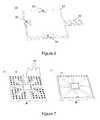
- FIG. 3provides an exploded perspective view of another embodiment illustrating major constituent elements of the construction.
- FIG. 4provides perspective views of the elements shown in FIG. 3 in a partially assembled form and an enlargement of a section, to show greater detail.
- FIG. 5illustrates, in a perspective view, an embodiment of the invention wherein more than 1 chip is interconnected within the package.
- FIG. 6illustrates, in a perspective view, an embodiment of the invention wherein the assembly is encapsulated and having contacts disposed for connection, both at the edge of the package and extending beyond the edge of the package on a length of circuit greater than the other lengths.
- FIGS. 7A and 7Bprovide perspective views of partially assembled embodiments having circuits on the upper surface which egress at differing angles and directions.
- FIG. 8illustrates an embodiment in cross section showing prospective elements of construction and having wire bonds made directly to a stripline circuit construction which exits the package on the edge.
- FIG. 9illustrates an embodiment wherein more than one cable is mounted and interconnected to a surface opposite of the IC in a package.
- FIG. 10illustrates an embodiment wherein the separate circuit is extended, folded back and bonded to the encapsulation which protects the IC chip.
- FIG. 11illustrates an embodiment wherein the separate circuit is extended, folded back and bonded to the encapsulation, which protects the IC chip and having also a second IC chip interconnect to the circuit, and the circuit then extending to make interconnection to another electronic device or element.
- FIG. 12provides an example of embodiment wherein multiple devices of varying embodiments are in process of assembly to a substrate and have interconnections to another element such as a cable or data bus.
- FIG. 13provides a perspective view of an assembly comprised of various component embodiments, circuit elements and interconnection support pedestals which serve as separable or permanent connectors.
- FIG. 14provides a perspective view of an embodiment disposed to having a connector on IC package before being provided with a locking lever and an enlarged area providing detail of the contacts.
- FIG. 15provides the perspective view of an embodiment having a connector on IC package with a locking lever and a circuit assembly disposed for mating with the IC package connector.
- FIG. 16is an illustration of a cross sectioned view through the middle of the IC package and the circuit assembly.
- FIGS. 17A-17Care a close up series of images illustrating the operation of the connector mechanism.
- FIG. 18illustrates gold bumps viewed through the flexible circuit assembly.
- FIG. 19is an illustration of the back of the locking lever in a perspective view.
- FIG. 20provides a perspective view of a partially assembled pedestal connector with one side engaged to a circuit and the second side disposed for interconnection.
- FIG. 21provides a perspective view of a partially assembled pedestal connector of FIG. 20 from the opposite side, showing circuits and having an enlarged area to provide greater detail of the contact area.
- circuit elements or circuit blocksmay be shown or described as multi-conductor or single conductor signal lines.
- Each of the multi-conductor signal linesmay alternatively be single-conductor signal lines, and each of the single-conductor signal lines may alternatively be multi-conductor signal lines.
- Signals and signaling paths shown or described as being single-endedmay also be differential, and vice-versa.
- the interconnecting structuresmay be microstrip or stripline and the signal lines may be either shielded or unshielded.
- Some or all high-speed signals, low-speed signals, power or groundmay be routed from one integrated circuit package to the other via the circuit or cable, while other signals, power or ground may be routed to the integrated circuit packages via traces and conductive structures that route through the printed circuit board.
- I/O driversare connected directly to those signal lines and transmitted through the cable or circuit to the surface of the second chip package.
- Such added cable or circuit structureswould provide the paths for some or all high speed signals either proximate to the edge of the body of the package or beyond the edge of the package to a location intermediate between the edge of the package and the chip where interconnections can be made to a terminal block or connector of a design which does not degrade the signal quality.
- an embodimentcould also provide a top circuit layer structure directly from the chip, off of and away from, the perimeter of the package. Some embodiments may carry the signal away from the chip starting at the chip itself, the bond wire, or the bond pad on the package.
- the top circuit layer structurecould be made of reinforced materials or non-reinforced materials (i.e., rigid to flexible) and could be made of various materials matching the electrical needs of the application.
- FIGS. 1A and 1Bdepict a prior-art embodiment of an IC package 3 including an IC die 15 mounted in the center of an IC package substrate 10 .
- the IC Package of FIGS. 1A and 1Bhas been modified in accordance with an embodiment of the invention described in U.S. patent application Ser. No. 10/426,930, which is incorporated by reference herein.
- selected circuit traces 13are disposed on the top surface of the package substrate.
- the circuit traces 13terminate in first and second ends. The terminations at the first end are positioned near the center of the IC package, for connection to an IC die.
- the second end of each circuit traceterminates somewhere between the IC die 15 and the edge of the substrate 10 .
- FIG. 1Bdepicts a cross sectional view of the IC package 3 of FIG. 1A , and illustrates a prospective construction, where a flexible or rigid circuit structure 10 , such as an IC package substrate, comprises an insulating dielectric base material 12 which has conductive circuit traces 13 with corresponding first and second ends. The circuit traces are, partially protected by a second insulating dielectric material 14 of suitable properties.
- An IC die 15is attached to the base circuit structure 10 , which can have one or more layers of interconnection wiring comprising internal layers (not shown) and interconnected to traces thereon by means of wire bonds 16 .
- the IC diecan be mounted directly to an IC package substrate by flip chip technology that utilizes conductive “bumps,” thereby eliminating the need for bond wires 16 .
- IC die and bond wiresare protected by an encapsulant 17 .
- Next level connection from the IC package to a structure such as a PCBcan be accomplished by a variety of contacts, such as solder balls 18 depicted in FIG. 1 B.
- a second circuit 19such as a flexible circuit or cable, is attached to the opposite (e.g. upper) surface using a suitable means such as solder or conductive adhesive or by a separable connection (not shown).
- the circuit 19can be, but is not limited to, a microstrip or stripline construction and can also be of unshielded differential pairs or single ended or coaxial connections if so desired.
- One or more of the separate circuits 19can be mounted on the otherwise unmodified IC package substrate on one or both sides if desired.
- FIG. 2Aillustrates top plan view of an embodiment of an otherwise unmodified IC package structure 25 that includes a substrate 20 , an IC die 41 disposed in the center of the substrate, and a circuit structure 21 coupled with the substrate.
- the circuit structure 21is comprised of three circuit arms (e.g., flexible circuits). Each circuit arm has a proximal end disposed proximate the IC die 41 and a distal end extending beyond the outer edge of the substrate 20 . Each circuit arm 21 has at least one circuit trace, which extends the length of the arm on which it is located, from a first termination site 22 at the distal end of its arm, to a second termination site 23 at the proximal end of its arm.
- FIG. 2Adepicts a circuit structure 21 comprised of three flexible circuit arms. However, the circuit structure could be comprised of a single circuit arm or a plurality of circuit arms.
- FIGS. 2B and 2Cdepict cross sectional views of alternative embodiments of the IC package structure 25 depicted in FIG. 2A .
- the IC package structure 25 ( b )has IC package terminations 18 (e.g. solder balls 18 ) on the same side of the package as the circuit structure(s) 21 .
- the circuit structures 21are coupled to corresponding IC die-terminals 43 by bond wires 42 .
- FIG. 2Cdepicts a cross sectional view of an embodiment 25 ( c ) of the IC package structure 25 of FIG. 2A , wherein IC die terminations 43 are on one surface (e.g. top surface) of the IC die 41 , and package terminations 18 are on the side opposite of the IC die, which, in FIG. 2C , is the bottom surface of the IC package substrate). Interconnection between the top and bottom surfaces of the IC package substrate 20 is achieved by conductive pathways such as plated through holes. Circuit structure 21 is attached to the IC package on the same side as the IC die terminals 43 . The conductive path(s) of circuit structure 21 are interconnected to the IC die or chip terminals by means of bond wires 42 .
- FIG. 3provides a perspective view of an IC package substrate 20 and a circuit structure 30 configured for attachment to the IC package substrate.
- the substratehas a center region configured to accommodate at least one IC die.
- the separately constructed circuit structure 30has four arms 31 a , 31 b , 31 c , 31 d , each arm having an proximal end and distal end. Each arm contains conductive circuit traces extending from its proximal end to its distal end.
- the circuit structureis configured such that, when attached to the package substrate 20 , the proximal end of each arm is disposed near the IC die.
- each arm 31 a - 31 cincludes one or more conductive circuit traces 32 , 34 .
- Each circuit tracehas a first termination near the proximal end of its respective arm, and a second termination near the distal end of its respective arm.
- FIG. 4illustrates a perspective view of an embodiment in which the assembly of the IC package and the circuit structure shown in FIG. 3 , comprises an IC die 41 wired bonded to the circuit structure 30 to create a partially completed assembly 40 .
- An enlarged detail sectionshows contacts being made by wires 42 directly from first terminations on the chip 43 to second terminations 34 on the attached circuit structure 30 .
- stacking of additional IC die atop the firstis also possible and can be used in combination with the stacking of additional circuit layer if so desired.
- Such additional circuit layerscould also include coiled inductors and wireless antenna.
- FIG. 5illustrates an assembly embodiment 50 with separate circuit structure 30 having additional IC chips 51 mounted and interconnected to it using a suitable method (e.g. flip chip interconnection) and positioned between the IC 41 and the circuit paths with their terminations.
- a suitable methode.g. flip chip interconnection
- Such chipscould provide extra functionality or improve signal performance with external drivers.
- stacking of IC chips one atop another and then interconnected to the combined structure package (not shown)is also possible to provide extra functionality.
- FIG. 6illustrates the embodiment illustrated in FIG. 5 further processed to create a more complete assembly 60 , having an encapsulant or overmold material 61 applied over the assembly to protect the IC chip mounted on and interconnected to both the unmodified IC package substrate and separate circuit 30 , and leaving terminal locations 62 for the circuits open and free of encapsulant.
- FIG. 7Adepicts a prospective view of an alternative embodiment for an assembly comprising a circuit structure 74 disposed on a surface of an integrated circuit package substrate 70 .
- Circuit structure 74includes features such as generally described in the foregoing FIGS. 2-6 , but includes eight arms 72 extending away from the location of the central IC die in varying discrete directions, allowing for circuit paths to be routed at any desired angle. The distal end of some of the arms 72 of FIG. 7 extend to the edge of the IC package substrate 70 . Other arms 72 terminate before reaching the edge of the IC package substrate.
- FIG. 7Bdepicts an alternative embodiment of a circuit structure 73 in assembly with an IC package.
- the circuit structureis a monolithic structure 73 having no individual arms extending from a center area.
- the circuit structure 73has circuits routable along any desired path on its surface.
- the circuit structure 73 of FIG. 7Bcould also serve as a foundation for a coil or like structures. Any of the separate circuits could be constructed with perforations in them (not shown) that may improve bonding to the IC package and the flow and fill of any adhesives that might be used in the bonding process. Perforations may also facilitate and/or improve bonding of the overmolding or encapsulating material used to protect the IC and its interconnections.
- FIG. 8illustrates an embodiment comprising an unmodified IC package substrate 80 comprising an insulating dielectric base material 82 , with an IC chip 81 mounted thereon.
- Circuit paths 86 on the base material of the packageterminate on the package at a solder ball terminal 88 , and the IC chip 81 is interconnected to the circuit paths on the package by means of wire bonds 83 .
- the mounted and bonded separate circuit 89shown in the image has a three metal conductor layer stripline circuit.
- the separate circuit 89has a first end disposed on the substrate surface proximate the IC chip 81 , and extends beyond the perimeter of the IC package interconnection substrate.
- the separate circuit 89is also interconnected to the chip by means of a separate wire bond 84 .
- the chip, bonded separate circuit and the interconnectionsare protected by an encapsulant 87 .
- FIG. 9illustrates an embodiment wherein the separate circuits 95 , shown in the figure as stripline circuits, are bonded and interconnected circuit paths 92 b using an interconnection material such as solder or conductive adhesive 94 .
- An interconnection pathis made to the flip chip IC 91 on the opposite side of the package substrate by way of vias 93 passing through the IC package to the surface opposite the strip line circuits.
- the side having the flip chipalso has circuit paths 92 a to be mounted to a next level interconnection substrate.
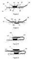
- FIG. 10illustrates an embodiment wherein the separate circuit 100 is extended, folded back and bonded to the encapsulated chip and circuit using an adhesive 101 and having terminals 102 to provide a larger or more stable platform for interconnecting to and routing signals to one or more other IC chip packages distant or proximate to the first IC chip package.
- FIG. 11illustrates an embodiment wherein a bonded separate circuit (e.g., a stripline circuit) 100 has an extended length separate circuit and a separate IC chip or package 111 mounted on the separate circuit to provide either greater functionality or performance.
- the extended length separate circuitis bonded to the top of the encapsulated package using an adhesive 101 .
- FIG. 12illustrates a partially assembled embodiment showing potential interconnection methods for some of the various described embodiments of finished parts.
- a base interconnection structure or printed circuit 121has disposed for interconnection four package structures 120 a , 120 b , 120 c and 120 d , each having integral separate circuit extensions 30 and openings 61 allowing interconnections to be made either to one another or to other separate interconnecting structures, such as a common bus cable 122 or other interconnecting structure.
- FIG. 13shows a perspective view of another assembly embodiment 130 comprised of a base circuit structure 131 and four interconnected package structures 132 a , 132 b , 132 c and 132 d . While only four packages are shown, it will be readily appreciated that many packages are possible.
- the packagesare interconnected by means of discrete circuit elements 133 , 134 , 135 of varying shapes and lengths. For example, section 133 is straight, 134 is curved and 135 is bifurcated. Also show are pedestals 136 which serve to support and interconnect the partial circuits.
- the pedestalscan be of insulating material (e.g., polymer ceramic or glass), conductive material (e.g., metal or metal filled polymers), semi-conductive materials (e.g., silicon) or combinations thereof.
- the pedestalsserve to support and can also align circuits they interconnect and can be used to make either permanent or temporary/separable connections.
- FIG. 14shows a perspective view of an embodiment of an IC package assembly 140 comprising a base circuit 141 and a central die 142 and encapsulated with a suitable material 143 , but having at least one open area 145 with exposed electrical contacts 146 .
- An enlarged detail view 147shows the contacts provided with conductive bumps 148 if desired.
- the encapsulating material 143is disposed with a hinge position 144 .
- FIG. 15shows assembly 140 with a locking lever 155 in place and in an open position. Also shown is a partial view of a circuit assembly 150 disposed for mating to the IC package.
- Circuit assembly 150has a base circuit 151 which may be a flexible circuit and has a stiffener 152 affixed to the base circuit. The stiffener can also serve as an alignment mechanism, such as providing a slot thereon which would capture a pin on the mating assembly (not shown).
- FIG. 16illustrates a cross sectioned view through the middle of assembly 140 and the circuit assembly 150 .
- the circuit assembly 150has been inserted under locking lever 155 .
- notch 153 in stiffener 152touches stop 161 , the circuit assembly 150 is in position for the next operation.
- FIGS. 17A-17Cillustrate, in close-up cross section views, selected elements of FIG. 16 showing detail of the operation.
- FIG. 17Ashows of the locking lever 155 of the assembly 140 disposed above the stiffener 152 of circuit assembly 150 .
- the locking levercomprises a stop 161 which, according to the position of FIG. 17A , extends into a notch 153 formed at the distal end of the stiffener.
- the horizontal surface of the notchterminates at a vertical surface of the stiffener 152 , which is abutted against the locking lever stop 161 .
- FIG. 17Bshows the locking lever 155 partially rotated toward the fully locked position.
- the pulls 173are just beginning to engage the notches 174 .
- FIG. 17Cshows the locking lever 155 in the fully locked position.
- the pulls 173have pulled the flexible circuit assembly into the IC package.
- the cam surface 175 on the locking lever 155pushes down on the top of the sitffener 152 , thus forcing the flexible circuit's contact pads downward.
- FIG. 18shows a hidden section view through the top of assembly 140 and circuit assembly 150 .
- the sectionenables us to view the locations of the electrical contacts 148 on assembly 140 , and the electrical contacts 171 on the circuit assembly 150 .
- the electrical contactsprovide more than one contact per signal interconnection and are designed to eliminate the capacitive stub common when only one electrical contact is present per signal interconnection.
- the electrical contactsmay be conductive dots or bumps of gold or other suitable corrosion resistant contact metal. The dots or bumps serve to connect with electrical contact pads.
- FIGS. 17A-17Cillustrate how the contacts on each side of the interconnection interface move with respect to each other to provide contact wipe.
- FIG. 19provides a rear view of the locking lever 155 .
- the stop 161 , pulls 173 , and cam surface 175 of the locking lever 155are shown. While members of the locking lever are shown as having defined dimensions for the illustration, they are not limited in size, shape or location on the locking lever nor are the size, shape or location of corresponding mating notches on the stiffener 152 with the major concern being that their primary functions are fulfilled.
- FIG. 20illustrates a partially assembled embodiment 200 of the pedestal interconnection devices 136 shown in FIG. 13 .
- a pedestal connector 136serves to electrically interconnect circuit assemblies 150 , which are disposed to be positioned within the saddle of the body of the pedestal.
- Locking levers 155 a , 155 bare positioned back to back and have the same basic functions and configurations as locking lever 155 shown in FIGS. 15 , 16 , 17 A-C and 19 .
- locking lever 155 ais shown in the open position and disposed for connecting to circuit assembly 150 A, while locking lever 155 b is shown in the closed position with the circuit assembly 150 B connected and locked into position.
- Circuit substrate 203resides inside connector housing 206 , and has a set of exposed electrical contacts 204 with conductive bumps 205 at or proximate to the end of the conductors. Conductive bumps 205 are similar to those items 146 , 148 respectively shown in FIG. 14 . There is an unseen, mirror image of electrical contacts with conductive bumps under locking lever 155 b . The locking levers 155 a , 155 b provide the force required to electrically interconnect circuit assemblies 150 through circuit substrate 203 . Either or both circuit assemblies 150 may be electrically attached to IC packages or other electrical components and provide electrical function such as a ground function. Circuit assemblies 150 can also be provided with alignment features such as slots which would capture pins on the pedestal (not shown).
- FIG. 21illustrates an isometric view from the bottom of the partially assembled structure 200 .
- pedestal electrical connector 136is coupled with circuit assemblies 150 A, 150 B.
- Conductive bumps 171are at the ends of the circuit assemblies' electrical contact pads.
- Posts 210may be integral with the connector housing 206 may be positioned into holes in a printed circuit board or the like (not shown). These posts or additional posts on the bottom of the connector housing may be conductive and electrically connect electronic signals, ground or power, originating in the printed circuit board to the conductors in the circuit assemblies 150 and/or pedestal connector 136 or to conductors in the circuit substrate 203 .
- circuits bonded into the saddle of a pedestalWhile much discussion has be given to the use of circuits bonded into the saddle of a pedestal, it should be clear to those of average skill in the art that the circuit conductors could be molded into the body of the pedestal and that the shoulders which define the saddle are not a mandatory requirement.
- the locking leverwhen operated, may provide the contact force necessary for low contact resistance while simultaneously moving the contact with respect to the contact pad to produce contact wipe.
- Present known art relative to locking leversprovide no purposeful contact wipe, but instead commonly produce a butt contact which normally offers no contact wipe.
- butt contactrequires much larger contact forces than a contact with wiping action.
- the embodiments illustratedmay not require as much contact force as prior art.
- FIG. 18conductive bumps or conductive dots are placed at the ends of the contact pads in each circuit element. When the contacts are overlapped and electrically interconnected, they may fully or partially eliminate the capacitive stub that is typically created when only one conductive bump is present in the signal interconnection.
- FIG. 18illustrates contact redundancy for each signal interconnection.
- FIG. 18also illustrates alignment between the contacts in the direction defined by a line between the redundant contacts in the signal interconnection. In this embodiment, if one contact is farther away from or closer to the redundant contact in the signal interconnection, contact and signal integrity are still generally retained.
Landscapes
- Physics & Mathematics (AREA)
- Condensed Matter Physics & Semiconductors (AREA)
- General Physics & Mathematics (AREA)
- Engineering & Computer Science (AREA)
- Computer Hardware Design (AREA)
- Microelectronics & Electronic Packaging (AREA)
- Power Engineering (AREA)
- Details Of Connecting Devices For Male And Female Coupling (AREA)
- Combinations Of Printed Boards (AREA)
Abstract
Description
Claims (41)
Priority Applications (1)
| Application Number | Priority Date | Filing Date | Title |
|---|---|---|---|
| US11/182,484US7750446B2 (en) | 2002-04-29 | 2005-07-14 | IC package structures having separate circuit interconnection structures and assemblies constructed thereof |
Applications Claiming Priority (5)
| Application Number | Priority Date | Filing Date | Title |
|---|---|---|---|
| US37648202P | 2002-04-29 | 2002-04-29 | |
| US40018002P | 2002-07-31 | 2002-07-31 | |
| US10/426,930US7307293B2 (en) | 2002-04-29 | 2003-04-29 | Direct-connect integrated circuit signaling system for bypassing intra-substrate printed circuit signal paths |
| US58831204P | 2004-07-14 | 2004-07-14 | |
| US11/182,484US7750446B2 (en) | 2002-04-29 | 2005-07-14 | IC package structures having separate circuit interconnection structures and assemblies constructed thereof |
Related Parent Applications (1)
| Application Number | Title | Priority Date | Filing Date |
|---|---|---|---|
| US10/426,930Continuation-In-PartUS7307293B2 (en) | 2002-04-29 | 2003-04-29 | Direct-connect integrated circuit signaling system for bypassing intra-substrate printed circuit signal paths |
Publications (2)
| Publication Number | Publication Date |
|---|---|
| US20060091507A1 US20060091507A1 (en) | 2006-05-04 |
| US7750446B2true US7750446B2 (en) | 2010-07-06 |
Family
ID=36260855
Family Applications (1)
| Application Number | Title | Priority Date | Filing Date |
|---|---|---|---|
| US11/182,484Expired - LifetimeUS7750446B2 (en) | 2002-04-29 | 2005-07-14 | IC package structures having separate circuit interconnection structures and assemblies constructed thereof |
Country Status (1)
| Country | Link |
|---|---|
| US (1) | US7750446B2 (en) |
Cited By (6)
| Publication number | Priority date | Publication date | Assignee | Title |
|---|---|---|---|---|
| US20090204195A1 (en)* | 2005-12-12 | 2009-08-13 | Jacobsen Stephen C | Multi-Element Probe Array |
| US20100112865A1 (en)* | 2005-12-12 | 2010-05-06 | Jacobsen Stephen C | Ultra-High Density Connector |
| US20100116869A1 (en)* | 2005-12-12 | 2010-05-13 | Jacobsen Stephen C | Electrical Microfilament to Circuit Interface |
| US20130045611A1 (en)* | 2011-08-18 | 2013-02-21 | Tyco Electronics Corporation | Electronic module packages and communication assemblies |
| US20190150311A1 (en)* | 2017-11-13 | 2019-05-16 | Te Connectivity Corporation | Socket connector for an electronic package |
| US11621237B2 (en)* | 2019-01-14 | 2023-04-04 | Intel Corporation | Interposer and electronic package |
Families Citing this family (44)
| Publication number | Priority date | Publication date | Assignee | Title |
|---|---|---|---|---|
| AU2003223783A1 (en)* | 2002-04-29 | 2003-11-17 | Silicon Pipe, Inc. | Direct-connect signaling system |
| US7750446B2 (en) | 2002-04-29 | 2010-07-06 | Interconnect Portfolio Llc | IC package structures having separate circuit interconnection structures and assemblies constructed thereof |
| US7425760B1 (en)* | 2004-10-13 | 2008-09-16 | Sun Microsystems, Inc. | Multi-chip module structure with power delivery using flexible cables |
| US7518238B2 (en)* | 2005-12-02 | 2009-04-14 | Intel Corporation | Mounting flexible circuits onto integrated circuit substrates |
| US7569916B2 (en)* | 2006-03-14 | 2009-08-04 | Paricon Technologies Corp. | Separable network interconnect systems and assemblies |
| DE102008012913A1 (en)* | 2008-03-06 | 2009-09-10 | Valeo Schalter Und Sensoren Gmbh | Electrical component or device with a flexible printed circuit board |
| KR101030991B1 (en)* | 2008-12-31 | 2011-04-22 | 삼성에스디아이 주식회사 | Mounting structure of semiconductor package and plasma display device |
| EP2204848A1 (en)* | 2008-12-31 | 2010-07-07 | Samsung SDI Co., Ltd. | Semiconductor Package and Plasma Display Device including the same |
| KR101030990B1 (en)* | 2008-12-31 | 2011-04-22 | 삼성에스디아이 주식회사 | Semiconductor package and plasma display device having same |
| US9011177B2 (en) | 2009-01-30 | 2015-04-21 | Molex Incorporated | High speed bypass cable assembly |
| US8354300B2 (en)* | 2010-02-23 | 2013-01-15 | Qualcomm Incorporated | Reducing susceptibility to electrostatic discharge damage during die-to-die bonding for 3-D packaged integrated circuits |
| US20130181360A1 (en)* | 2012-01-18 | 2013-07-18 | Xilinx, Inc. | Integrated circuit connectivity using flexible circuitry |
| US9240644B2 (en) | 2012-08-22 | 2016-01-19 | Amphenol Corporation | High-frequency electrical connector |
| US9142921B2 (en) | 2013-02-27 | 2015-09-22 | Molex Incorporated | High speed bypass cable for use with backplanes |
| CN105580210B (en) | 2013-09-04 | 2017-07-07 | 莫列斯有限公司 | Connector system with bypass cable |
| US9685736B2 (en) | 2014-11-12 | 2017-06-20 | Amphenol Corporation | Very high speed, high density electrical interconnection system with impedance control in mating region |
| KR102120813B1 (en) | 2015-01-11 | 2020-06-17 | 몰렉스 엘엘씨 | Circuit board bypass assembly and components therefor |
| WO2016112384A1 (en) | 2015-01-11 | 2016-07-14 | Molex, Llc | Wire to board connectors suitable for use in bypass routing assemblies |
| WO2016179263A1 (en) | 2015-05-04 | 2016-11-10 | Molex, Llc | Computing device using bypass assembly |
| US10424856B2 (en) | 2016-01-11 | 2019-09-24 | Molex, Llc | Routing assembly and system using same |
| TWI625010B (en) | 2016-01-11 | 2018-05-21 | Molex Llc | Cable connector assembly |
| TWI597896B (en) | 2016-01-19 | 2017-09-01 | Molex Llc | Integrated routing components |
| TWI746561B (en) | 2016-05-31 | 2021-11-21 | 美商安芬諾股份有限公司 | High performance cable termination |
| CN110088985B (en) | 2016-10-19 | 2022-07-05 | 安费诺有限公司 | Flexible shield for ultra-high speed high density electrical interconnects |
| TWI788394B (en) | 2017-08-03 | 2023-01-01 | 美商安芬諾股份有限公司 | Cable assembly and method of manufacturing the same |
| US20190051587A1 (en)* | 2017-08-11 | 2019-02-14 | Marvell Israel (M.I.S.L) Ltd. | Ic package |
| TWI833717B (en) | 2017-11-14 | 2024-03-01 | 美商山姆科技公司 | Connector, data communication system, method of mounting connector, electrical component and method of constructing electrical component |
| US11508663B2 (en) | 2018-02-02 | 2022-11-22 | Marvell Israel (M.I.S.L) Ltd. | PCB module on package |
| US10665973B2 (en) | 2018-03-22 | 2020-05-26 | Amphenol Corporation | High density electrical connector |
| WO2019195319A1 (en) | 2018-04-02 | 2019-10-10 | Ardent Concepts, Inc. | Controlled-impedance compliant cable termination |
| TWM611526U (en) | 2018-09-04 | 2021-05-11 | 美商山姆科技公司 | Interconnect system |
| US10931062B2 (en) | 2018-11-21 | 2021-02-23 | Amphenol Corporation | High-frequency electrical connector |
| WO2020154507A1 (en) | 2019-01-25 | 2020-07-30 | Fci Usa Llc | I/o connector configured for cable connection to a midboard |
| US11101611B2 (en) | 2019-01-25 | 2021-08-24 | Fci Usa Llc | I/O connector configured for cabled connection to the midboard |
| WO2020172395A1 (en) | 2019-02-22 | 2020-08-27 | Amphenol Corporation | High performance cable connector assembly |
| WO2020250162A1 (en) | 2019-06-10 | 2020-12-17 | Marvell Israel (M.I.S.L) Ltd. | Ic package with top-side memory module |
| CN114788097A (en) | 2019-09-19 | 2022-07-22 | 安费诺有限公司 | High speed electronic system with midplane cable connector |
| TWI887339B (en) | 2020-01-27 | 2025-06-21 | 美商Fci美國有限責任公司 | High speed, high density direct mate orthogonal connector |
| WO2021154702A1 (en) | 2020-01-27 | 2021-08-05 | Fci Usa Llc | High speed connector |
| CN113258325A (en) | 2020-01-28 | 2021-08-13 | 富加宜(美国)有限责任公司 | High-frequency middle plate connector |
| US20220140514A1 (en)* | 2020-11-02 | 2022-05-05 | Samtec, Inc. | Flex Circuit And Electrical Communication Assemblies Related To Same |
| WO2022226873A1 (en)* | 2021-04-29 | 2022-11-03 | 华为技术有限公司 | Circuit board assembly part and electronic device |
| USD1002553S1 (en) | 2021-11-03 | 2023-10-24 | Amphenol Corporation | Gasket for connector |
| DE102023209356A1 (en)* | 2023-09-25 | 2025-03-27 | Fraunhofer-Gesellschaft zur Förderung der angewandten Forschung eingetragener Verein | Detachable connector for a flexible waveguide |
Citations (118)
| Publication number | Priority date | Publication date | Assignee | Title |
|---|---|---|---|---|
| US3795845A (en) | 1972-12-26 | 1974-03-05 | Ibm | Semiconductor chip having connecting pads arranged in a non-orthogonal array |
| US4095866A (en) | 1977-05-19 | 1978-06-20 | Ncr Corporation | High density printed circuit board and edge connector assembly |
| US4202007A (en) | 1978-06-23 | 1980-05-06 | International Business Machines Corporation | Multi-layer dielectric planar structure having an internal conductor pattern characterized with opposite terminations disposed at a common edge surface of the layers |
| US4302501A (en) | 1975-12-24 | 1981-11-24 | Koreyuki Nagashima | Porous, heat resistant insulating substrates for use in printed circuit boards, printed circuit boards utilizing the same and method of manufacturing insulating substrates and printed circuit boards |
| US4445735A (en) | 1980-12-05 | 1984-05-01 | Compagnie Internationale Pour L'informatique Cii-Honeywell Bull (Societe Anonyme) | Electrical connection device for high density contacts |
| US4458297A (en) | 1981-01-16 | 1984-07-03 | Mosaic Systems, Inc. | Universal interconnection substrate |
| US4543715A (en) | 1983-02-28 | 1985-10-01 | Allied Corporation | Method of forming vertical traces on printed circuit board |
| US4551673A (en) | 1980-10-13 | 1985-11-05 | Riba-Pruftechnik Gmbh | Testing arrangement for printed circuit boards |
| US4636919A (en) | 1985-03-20 | 1987-01-13 | Hitachi, Ltd. | Multilayer printed circuit board |
| US4644092A (en) | 1985-07-18 | 1987-02-17 | Amp Incorporated | Shielded flexible cable |
| US4675243A (en) | 1983-02-25 | 1987-06-23 | Shinko Electric Industries Co., Ltd. | Ceramic package for semiconductor devices |
| US4730159A (en) | 1984-06-21 | 1988-03-08 | The General Electric Company P.L.C. | Programmable bed-of-nails test access jigs |
| US4731643A (en) | 1985-10-21 | 1988-03-15 | International Business Machines Corporation | Logic-circuit layout for large-scale integrated circuits |
| US4748495A (en) | 1985-08-08 | 1988-05-31 | Dypax Systems Corporation | High density multi-chip interconnection and cooling package |
| US4768154A (en) | 1987-05-08 | 1988-08-30 | Telesis Systems Corporation | Computer aided printed circuit board wiring |
| US4799617A (en) | 1987-10-09 | 1989-01-24 | Advanced Techniques Co., Inc. | Convection heat attachment and removal instrument for surface mounted assemblies |
| US4812792A (en) | 1983-12-22 | 1989-03-14 | Trw Inc. | High-frequency multilayer printed circuit board |
| US4814945A (en) | 1987-09-18 | 1989-03-21 | Trw Inc. | Multilayer printed circuit board for ceramic chip carriers |
| US4838800A (en) | 1988-05-23 | 1989-06-13 | Gte Products Corporation | High density interconnect system |
| US4861251A (en) | 1988-02-29 | 1989-08-29 | Diehard Engineering, Inc. | Apparatus for encapsulating selected portions of a printed circuit board |
| US4881905A (en) | 1986-05-23 | 1989-11-21 | Amp Incorporated | High density controlled impedance connector |
| US4912603A (en) | 1985-12-09 | 1990-03-27 | Fujitsu Limited | High density printed wiring board |
| US4935584A (en) | 1988-05-24 | 1990-06-19 | Tektronix, Inc. | Method of fabricating a printed circuit board and the PCB produced |
| US4956749A (en) | 1987-11-20 | 1990-09-11 | Hewlett-Packard Company | Interconnect structure for integrated circuits |
| US4960386A (en) | 1989-10-17 | 1990-10-02 | Molex Incorporated | High deflection, high density single sided electrical connector |
| US4969826A (en) | 1989-12-06 | 1990-11-13 | Amp Incorporated | High density connector for an IC chip carrier |
| US4982311A (en) | 1987-09-29 | 1991-01-01 | Bull S.A. | Package for very large scale integrated circuit |
| US4991115A (en) | 1989-05-16 | 1991-02-05 | Excellon Industries, Inc. | Method of mapping geometric entities from a continuous plane to a discrete plane |
| US4994938A (en) | 1988-12-28 | 1991-02-19 | Texas Instruments Incorporated | Mounting of high density components on substrate |
| US5009611A (en) | 1990-05-23 | 1991-04-23 | Molex Incorporated | High density electrical connector for printed circuit boards |
| US5012924A (en) | 1990-03-19 | 1991-05-07 | R. H. Murphy Company, Inc. | Carriers for integrated circuits and the like |
| US5019946A (en) | 1988-09-27 | 1991-05-28 | General Electric Company | High density interconnect with high volumetric efficiency |
| US5136123A (en) | 1987-07-17 | 1992-08-04 | Junkosha Co., Ltd. | Multilayer circuit board |
| US5155577A (en) | 1991-01-07 | 1992-10-13 | International Business Machines Corporation | Integrated circuit carriers and a method for making engineering changes in said carriers |
| US5162792A (en) | 1990-08-03 | 1992-11-10 | American Telephone And Telegraph Company | On-the-fly arrangement for interconnecting leads and connectors |
| US5165984A (en) | 1991-07-30 | 1992-11-24 | At&T Bell Laboratories | Stepped multilayer interconnection apparatus and method of making the same |
| US5185502A (en) | 1989-12-01 | 1993-02-09 | Cray Research, Inc. | High power, high density interconnect apparatus for integrated circuits |
| US5220490A (en) | 1990-10-25 | 1993-06-15 | Microelectronics And Computer Technology Corporation | Substrate interconnect allowing personalization using spot surface links |
| US5222014A (en) | 1992-03-02 | 1993-06-22 | Motorola, Inc. | Three-dimensional multi-chip pad array carrier |
| US5227013A (en) | 1991-07-25 | 1993-07-13 | Microelectronics And Computer Technology Corporation | Forming via holes in a multilevel substrate in a single step |
| US5291375A (en) | 1991-09-30 | 1994-03-01 | Kabushiki Kaisha Toshiba | Printed circuit board and electric device configured to facilitate bonding |
| US5309324A (en) | 1991-11-26 | 1994-05-03 | Herandez Jorge M | Device for interconnecting integrated circuit packages to circuit boards |
| US5319224A (en) | 1989-10-11 | 1994-06-07 | Mitsubishi Denki Kabushiki Kaisha | Integrated circuit device having a geometry to enhance fabrication and testing and manufacturing method thereof |
| US5417577A (en) | 1992-09-23 | 1995-05-23 | At&T Corp. | Interconnection method and apparatus |
| US5424492A (en) | 1994-01-06 | 1995-06-13 | Dell Usa, L.P. | Optimal PCB routing methodology for high I/O density interconnect devices |
| US5441917A (en) | 1992-07-17 | 1995-08-15 | Lsi Logic Corporation | Method of laying out bond pads on a semiconductor die |
| US5490040A (en) | 1993-12-22 | 1996-02-06 | International Business Machines Corporation | Surface mount chip package having an array of solder ball contacts arranged in a circle and conductive pin contacts arranged outside the circular array |
| US5491364A (en) | 1994-08-31 | 1996-02-13 | Delco Electronics Corporation | Reduced stress terminal pattern for integrated circuit devices and packages |
| US5498767A (en) | 1994-10-11 | 1996-03-12 | Motorola, Inc. | Method for positioning bond pads in a semiconductor die layout |
| US5500862A (en) | 1993-10-29 | 1996-03-19 | Nec Corporation | Multi-layer digital circuit board with a test pattern section |
| US5544018A (en) | 1994-04-13 | 1996-08-06 | Microelectronics And Computer Technology Corporation | Electrical interconnect device with customizeable surface layer and interwoven signal lines |
| US5545301A (en) | 1993-04-23 | 1996-08-13 | Robert Bosch Gmbh | Sensor element for the determination of concentration of gas constituent(s) |
| US5565706A (en) | 1994-03-18 | 1996-10-15 | Hitachi, Ltd. | LSI package board |
| US5578870A (en) | 1995-08-03 | 1996-11-26 | Precision Connector Designs, Inc. | Top loading test socket for ball grid arrays |
| US5584721A (en) | 1993-01-13 | 1996-12-17 | Sumitomo Wiring Systems, Ltd. | Connector |
| US5587944A (en) | 1996-03-18 | 1996-12-24 | Motorola | High density multistate SRAM and cell |
| US5596205A (en) | 1993-07-12 | 1997-01-21 | Peregrine Semiconductor Corporation | High-frequency wireless communication system on a single ultrathin silicon on sapphire chip |
| US5634093A (en) | 1991-01-30 | 1997-05-27 | Kabushiki Kaisha Toshiba | Method and CAD system for designing wiring patterns using predetermined rules |
| US5644500A (en) | 1994-03-18 | 1997-07-01 | Fujitsu Limited | Routing program generating method and apparatus therefor, placement program generating method and apparatus therefor, and automatic routing method and apparatus therefor |
| US5650662A (en)* | 1993-08-17 | 1997-07-22 | Edwards; Steven F. | Direct bonded heat spreader |
| US5684332A (en) | 1994-05-27 | 1997-11-04 | Advanced Semiconductor Engineering, Inc. | Method of packaging a semiconductor device with minimum bonding pad pitch and packaged device therefrom |
| US5686699A (en) | 1995-10-10 | 1997-11-11 | Acc Microelectronics Corporation | Semiconductor board providing high signal pin utilization |
| US5691569A (en) | 1995-12-20 | 1997-11-25 | Intel Corporation | Integrated circuit package that has a plurality of staggered pins |
| US5701233A (en) | 1995-01-23 | 1997-12-23 | Irvine Sensors Corporation | Stackable modules and multimodular assemblies |
| US5706178A (en) | 1995-12-20 | 1998-01-06 | Intel Corporation | Ball grid array integrated circuit package that has vias located within the solder pads of a package |
| US5715274A (en) | 1995-01-09 | 1998-02-03 | Lsi Logic Corporation | Method and system for communicating between a plurality of semiconductor devices |
| US5723906A (en) | 1996-06-07 | 1998-03-03 | Hewlett-Packard Company | High-density wirebond chip interconnect for multi-chip modules |
| US5729432A (en) | 1995-07-05 | 1998-03-17 | Anam Industrial Col, Ltd. | Ball grid array semiconductor package with improved heat dissipation and dehumidification effect |
| US5730606A (en) | 1996-04-02 | 1998-03-24 | Aries Electronics, Inc. | Universal production ball grid array socket |
| US5745374A (en) | 1994-07-22 | 1998-04-28 | Kabushiki Kaisha Toshiba | Layout method for semiconductor integrated circuit and layout apparatus for semiconductor integrated circuit |
| US5774340A (en) | 1996-08-28 | 1998-06-30 | International Business Machines Corporation | Planar redistribution structure and printed wiring device |
| US5781446A (en) | 1996-05-07 | 1998-07-14 | Flexible Solutions, Inc. | System and method for multi-constraint domain electronic system design mapping |
| US5784262A (en) | 1995-11-06 | 1998-07-21 | Symbios, Inc. | Arrangement of pads and through-holes for semiconductor packages |
| US5786631A (en) | 1995-10-04 | 1998-07-28 | Lsi Logic Corporation | Configurable ball grid array package |
| US5790383A (en) | 1996-02-20 | 1998-08-04 | Canon Kabushiki Kaisha | Printed circuit board |
| US5822214A (en) | 1994-11-02 | 1998-10-13 | Lsi Logic Corporation | CAD for hexagonal architecture |
| US5819403A (en) | 1994-03-11 | 1998-10-13 | The Panda Project | Method of manufacturing a semiconductor chip carrier |
| US5977640A (en) | 1998-06-26 | 1999-11-02 | International Business Machines Corporation | Highly integrated chip-on-chip packaging |
| US6031283A (en)* | 1996-09-09 | 2000-02-29 | Intel Corporation | Integrated circuit package |
| US6060772A (en) | 1997-06-30 | 2000-05-09 | Kabushiki Kaisha Toshiba | Power semiconductor module with a plurality of semiconductor chips |
| US6087732A (en) | 1998-09-28 | 2000-07-11 | Lucent Technologies, Inc. | Bond pad for a flip-chip package |
| US6121679A (en) | 1998-03-10 | 2000-09-19 | Luvara; John J. | Structure for printed circuit design |
| US6137064A (en) | 1999-06-11 | 2000-10-24 | Teradyne, Inc. | Split via surface mount connector and related techniques |
| US6150729A (en) | 1999-07-01 | 2000-11-21 | Lsi Logic Corporation | Routing density enhancement for semiconductor BGA packages and printed wiring boards |
| US6181718B1 (en) | 1997-01-08 | 2001-01-30 | Matsushita Electric Industrial Co., Ltd. | Electronically cooled semiconductor laser module with modified ground line inductance |
| US6264476B1 (en) | 1999-12-09 | 2001-07-24 | High Connection Density, Inc. | Wire segment based interposer for high frequency electrical connection |
| US6285560B1 (en) | 1999-09-20 | 2001-09-04 | Texas Instruments Incorporated | Method for increasing device reliability by selectively depopulating solder balls from a foot print of a ball grid array (BGA) package, and device so modified |
| US6304450B1 (en) | 1999-07-15 | 2001-10-16 | Incep Technologies, Inc. | Inter-circuit encapsulated packaging |
| US6310398B1 (en) | 1998-12-03 | 2001-10-30 | Walter M. Katz | Routable high-density interfaces for integrated circuit devices |
| US6310303B1 (en) | 1998-03-10 | 2001-10-30 | John J. Luvara | Structure for printed circuit design |
| US6388208B1 (en) | 1999-06-11 | 2002-05-14 | Teradyne, Inc. | Multi-connection via with electrically isolated segments |
| US6465336B2 (en) | 1997-04-09 | 2002-10-15 | Agere Systems Guardian Corp. | Circuit and method for providing interconnections among individual integrated circuit chips in a multi-chip module |
| US6507496B2 (en) | 2001-05-31 | 2003-01-14 | Intel Corporation | Module having integrated circuit packages coupled to multiple sides with package types selected based on inductance of leads to couple the module to another component |
| US20030048998A1 (en) | 2001-09-12 | 2003-03-13 | Yuan-Liang Li | Optical/electrical interconnects and package for high speed signaling |
| US6547570B2 (en) | 1998-06-23 | 2003-04-15 | Intel Corporation | IC package with quick connect feature |
| US6559531B1 (en) | 1999-10-14 | 2003-05-06 | Sun Microsystems, Inc. | Face to face chips |
| US20030095014A1 (en)* | 2001-11-21 | 2003-05-22 | Lao Binneg Y. | Connection package for high-speed integrated circuit |
| US20030098502A1 (en)* | 2001-05-17 | 2003-05-29 | Sharp Kabushiki Kaisha | Semiconductor package substrate, semiconductor package |
| US6603077B2 (en) | 2000-12-22 | 2003-08-05 | Canon Kabushiki Kaisha | Cable connection structure and electronic apparatus having the same |
| US6642808B2 (en) | 2000-05-30 | 2003-11-04 | Kyocera Corporation | High frequency package, wiring board, and high frequency module having a cyclically varying transmission characteristic |
| US20030222282A1 (en)* | 2002-04-29 | 2003-12-04 | Fjelstad Joseph C. | Direct-connect signaling system |
| US6686666B2 (en) | 2002-05-16 | 2004-02-03 | Intel Corporation | Breaking out signals from an integrated circuit footprint |
| US6704204B1 (en) | 1998-06-23 | 2004-03-09 | Intel Corporation | IC package with edge connect contacts |
| US6712648B2 (en)* | 2002-07-24 | 2004-03-30 | Litton Systems, Inc. | Laminate electrical interconnect system |
| US20040094328A1 (en) | 2002-11-16 | 2004-05-20 | Fjelstad Joseph C. | Cabled signaling system and components thereof |
| US20040113250A1 (en) | 2002-12-12 | 2004-06-17 | Khandros Igor Y. | Integrated circuit assembly |
| US6797891B1 (en) | 2002-03-18 | 2004-09-28 | Applied Micro Circuits Corporation | Flexible interconnect cable with high frequency electrical transmission line |
| US20040218372A1 (en)* | 2003-02-18 | 2004-11-04 | Hiroshi Hamasaki | LSI package provided with interface module and method of mounting the same |
| US20040227258A1 (en)* | 2003-05-14 | 2004-11-18 | Matsushita Electric Industrial Co., Ltd. | Electronic component packaging structure and method for producing the same |
| US6867668B1 (en) | 2002-03-18 | 2005-03-15 | Applied Micro Circuits Corporation | High frequency signal transmission from the surface of a circuit substrate to a flexible interconnect cable |
| US6882546B2 (en) | 2001-10-03 | 2005-04-19 | Formfactor, Inc. | Multiple die interconnect system |
| US20050087356A1 (en) | 2002-11-08 | 2005-04-28 | Robert Forcier | Build-up structures with multi-angle vias for chip to chip interconnects and optical bussing |
| US6893885B2 (en) | 2002-01-18 | 2005-05-17 | The Regents Of The University Of Michigan | Method for electrically and mechanically connecting microstructures using solder |
| US20050133929A1 (en) | 2003-12-18 | 2005-06-23 | Howard Gregory E. | Flexible package with rigid substrate segments for high density integrated circuit systems |
| US6977411B2 (en)* | 2002-12-20 | 2005-12-20 | Fujitsu Limited | Semiconductor device comprising transistors having control gates and floating gate electrodes |
| US6985659B2 (en) | 2003-06-30 | 2006-01-10 | Opnext Japan, Inc. | Optical transmission module |
| US20060091507A1 (en) | 2002-04-29 | 2006-05-04 | Fjelstad Joseph C | IC package structures having separate circuit interconnection structures and assemblies constructed thereof |
| US7345359B2 (en)* | 2004-03-05 | 2008-03-18 | Intel Corporation | Integrated circuit package with chip-side signal connections |
- 2005
- 2005-07-14USUS11/182,484patent/US7750446B2/ennot_activeExpired - Lifetime
Patent Citations (121)
| Publication number | Priority date | Publication date | Assignee | Title |
|---|---|---|---|---|
| US3795845A (en) | 1972-12-26 | 1974-03-05 | Ibm | Semiconductor chip having connecting pads arranged in a non-orthogonal array |
| US4302501A (en) | 1975-12-24 | 1981-11-24 | Koreyuki Nagashima | Porous, heat resistant insulating substrates for use in printed circuit boards, printed circuit boards utilizing the same and method of manufacturing insulating substrates and printed circuit boards |
| US4095866A (en) | 1977-05-19 | 1978-06-20 | Ncr Corporation | High density printed circuit board and edge connector assembly |
| US4202007A (en) | 1978-06-23 | 1980-05-06 | International Business Machines Corporation | Multi-layer dielectric planar structure having an internal conductor pattern characterized with opposite terminations disposed at a common edge surface of the layers |
| US4551673A (en) | 1980-10-13 | 1985-11-05 | Riba-Pruftechnik Gmbh | Testing arrangement for printed circuit boards |
| US4445735A (en) | 1980-12-05 | 1984-05-01 | Compagnie Internationale Pour L'informatique Cii-Honeywell Bull (Societe Anonyme) | Electrical connection device for high density contacts |
| US4458297A (en) | 1981-01-16 | 1984-07-03 | Mosaic Systems, Inc. | Universal interconnection substrate |
| US4675243A (en) | 1983-02-25 | 1987-06-23 | Shinko Electric Industries Co., Ltd. | Ceramic package for semiconductor devices |
| US4543715A (en) | 1983-02-28 | 1985-10-01 | Allied Corporation | Method of forming vertical traces on printed circuit board |
| US4812792A (en) | 1983-12-22 | 1989-03-14 | Trw Inc. | High-frequency multilayer printed circuit board |
| US4730159A (en) | 1984-06-21 | 1988-03-08 | The General Electric Company P.L.C. | Programmable bed-of-nails test access jigs |
| US4636919A (en) | 1985-03-20 | 1987-01-13 | Hitachi, Ltd. | Multilayer printed circuit board |
| US4644092A (en) | 1985-07-18 | 1987-02-17 | Amp Incorporated | Shielded flexible cable |
| US4748495A (en) | 1985-08-08 | 1988-05-31 | Dypax Systems Corporation | High density multi-chip interconnection and cooling package |
| US4731643A (en) | 1985-10-21 | 1988-03-15 | International Business Machines Corporation | Logic-circuit layout for large-scale integrated circuits |
| US4912603A (en) | 1985-12-09 | 1990-03-27 | Fujitsu Limited | High density printed wiring board |
| US4881905A (en) | 1986-05-23 | 1989-11-21 | Amp Incorporated | High density controlled impedance connector |
| US4768154A (en) | 1987-05-08 | 1988-08-30 | Telesis Systems Corporation | Computer aided printed circuit board wiring |
| US5136123A (en) | 1987-07-17 | 1992-08-04 | Junkosha Co., Ltd. | Multilayer circuit board |
| US4814945A (en) | 1987-09-18 | 1989-03-21 | Trw Inc. | Multilayer printed circuit board for ceramic chip carriers |
| US4982311A (en) | 1987-09-29 | 1991-01-01 | Bull S.A. | Package for very large scale integrated circuit |
| US4799617A (en) | 1987-10-09 | 1989-01-24 | Advanced Techniques Co., Inc. | Convection heat attachment and removal instrument for surface mounted assemblies |
| US4956749A (en) | 1987-11-20 | 1990-09-11 | Hewlett-Packard Company | Interconnect structure for integrated circuits |
| US4861251A (en) | 1988-02-29 | 1989-08-29 | Diehard Engineering, Inc. | Apparatus for encapsulating selected portions of a printed circuit board |
| US4838800A (en) | 1988-05-23 | 1989-06-13 | Gte Products Corporation | High density interconnect system |
| US4935584A (en) | 1988-05-24 | 1990-06-19 | Tektronix, Inc. | Method of fabricating a printed circuit board and the PCB produced |
| US5019946A (en) | 1988-09-27 | 1991-05-28 | General Electric Company | High density interconnect with high volumetric efficiency |
| US4994938A (en) | 1988-12-28 | 1991-02-19 | Texas Instruments Incorporated | Mounting of high density components on substrate |
| US4991115A (en) | 1989-05-16 | 1991-02-05 | Excellon Industries, Inc. | Method of mapping geometric entities from a continuous plane to a discrete plane |
| US5319224A (en) | 1989-10-11 | 1994-06-07 | Mitsubishi Denki Kabushiki Kaisha | Integrated circuit device having a geometry to enhance fabrication and testing and manufacturing method thereof |
| US4960386A (en) | 1989-10-17 | 1990-10-02 | Molex Incorporated | High deflection, high density single sided electrical connector |
| US5185502A (en) | 1989-12-01 | 1993-02-09 | Cray Research, Inc. | High power, high density interconnect apparatus for integrated circuits |
| US4969826A (en) | 1989-12-06 | 1990-11-13 | Amp Incorporated | High density connector for an IC chip carrier |
| US5012924A (en) | 1990-03-19 | 1991-05-07 | R. H. Murphy Company, Inc. | Carriers for integrated circuits and the like |
| US5009611A (en) | 1990-05-23 | 1991-04-23 | Molex Incorporated | High density electrical connector for printed circuit boards |
| US5162792A (en) | 1990-08-03 | 1992-11-10 | American Telephone And Telegraph Company | On-the-fly arrangement for interconnecting leads and connectors |
| US5220490A (en) | 1990-10-25 | 1993-06-15 | Microelectronics And Computer Technology Corporation | Substrate interconnect allowing personalization using spot surface links |
| US5155577A (en) | 1991-01-07 | 1992-10-13 | International Business Machines Corporation | Integrated circuit carriers and a method for making engineering changes in said carriers |
| US5634093A (en) | 1991-01-30 | 1997-05-27 | Kabushiki Kaisha Toshiba | Method and CAD system for designing wiring patterns using predetermined rules |
| US5227013A (en) | 1991-07-25 | 1993-07-13 | Microelectronics And Computer Technology Corporation | Forming via holes in a multilevel substrate in a single step |
| US5165984A (en) | 1991-07-30 | 1992-11-24 | At&T Bell Laboratories | Stepped multilayer interconnection apparatus and method of making the same |
| US5291375A (en) | 1991-09-30 | 1994-03-01 | Kabushiki Kaisha Toshiba | Printed circuit board and electric device configured to facilitate bonding |
| US5309324A (en) | 1991-11-26 | 1994-05-03 | Herandez Jorge M | Device for interconnecting integrated circuit packages to circuit boards |
| US5222014A (en) | 1992-03-02 | 1993-06-22 | Motorola, Inc. | Three-dimensional multi-chip pad array carrier |
| US5441917A (en) | 1992-07-17 | 1995-08-15 | Lsi Logic Corporation | Method of laying out bond pads on a semiconductor die |
| US5635424A (en) | 1992-07-17 | 1997-06-03 | Lsi Logic Corporation | High-density bond pad layout arrangements for semiconductor dies, and connecting to the bond pads |
| US5417577A (en) | 1992-09-23 | 1995-05-23 | At&T Corp. | Interconnection method and apparatus |
| US5584721A (en) | 1993-01-13 | 1996-12-17 | Sumitomo Wiring Systems, Ltd. | Connector |
| US5545301A (en) | 1993-04-23 | 1996-08-13 | Robert Bosch Gmbh | Sensor element for the determination of concentration of gas constituent(s) |
| US5596205A (en) | 1993-07-12 | 1997-01-21 | Peregrine Semiconductor Corporation | High-frequency wireless communication system on a single ultrathin silicon on sapphire chip |
| US5650662A (en)* | 1993-08-17 | 1997-07-22 | Edwards; Steven F. | Direct bonded heat spreader |
| US5500862A (en) | 1993-10-29 | 1996-03-19 | Nec Corporation | Multi-layer digital circuit board with a test pattern section |
| US5490040A (en) | 1993-12-22 | 1996-02-06 | International Business Machines Corporation | Surface mount chip package having an array of solder ball contacts arranged in a circle and conductive pin contacts arranged outside the circular array |
| US5424492A (en) | 1994-01-06 | 1995-06-13 | Dell Usa, L.P. | Optimal PCB routing methodology for high I/O density interconnect devices |
| US5819403A (en) | 1994-03-11 | 1998-10-13 | The Panda Project | Method of manufacturing a semiconductor chip carrier |
| US5644500A (en) | 1994-03-18 | 1997-07-01 | Fujitsu Limited | Routing program generating method and apparatus therefor, placement program generating method and apparatus therefor, and automatic routing method and apparatus therefor |
| US5565706A (en) | 1994-03-18 | 1996-10-15 | Hitachi, Ltd. | LSI package board |
| US5544018A (en) | 1994-04-13 | 1996-08-06 | Microelectronics And Computer Technology Corporation | Electrical interconnect device with customizeable surface layer and interwoven signal lines |
| US5684332A (en) | 1994-05-27 | 1997-11-04 | Advanced Semiconductor Engineering, Inc. | Method of packaging a semiconductor device with minimum bonding pad pitch and packaged device therefrom |
| US5745374A (en) | 1994-07-22 | 1998-04-28 | Kabushiki Kaisha Toshiba | Layout method for semiconductor integrated circuit and layout apparatus for semiconductor integrated circuit |
| US5491364A (en) | 1994-08-31 | 1996-02-13 | Delco Electronics Corporation | Reduced stress terminal pattern for integrated circuit devices and packages |
| US5498767A (en) | 1994-10-11 | 1996-03-12 | Motorola, Inc. | Method for positioning bond pads in a semiconductor die layout |
| US5822214A (en) | 1994-11-02 | 1998-10-13 | Lsi Logic Corporation | CAD for hexagonal architecture |
| US5715274A (en) | 1995-01-09 | 1998-02-03 | Lsi Logic Corporation | Method and system for communicating between a plurality of semiconductor devices |
| US5701233A (en) | 1995-01-23 | 1997-12-23 | Irvine Sensors Corporation | Stackable modules and multimodular assemblies |
| US5729432A (en) | 1995-07-05 | 1998-03-17 | Anam Industrial Col, Ltd. | Ball grid array semiconductor package with improved heat dissipation and dehumidification effect |
| US5578870A (en) | 1995-08-03 | 1996-11-26 | Precision Connector Designs, Inc. | Top loading test socket for ball grid arrays |
| US5786631A (en) | 1995-10-04 | 1998-07-28 | Lsi Logic Corporation | Configurable ball grid array package |
| US5686699A (en) | 1995-10-10 | 1997-11-11 | Acc Microelectronics Corporation | Semiconductor board providing high signal pin utilization |
| US5784262A (en) | 1995-11-06 | 1998-07-21 | Symbios, Inc. | Arrangement of pads and through-holes for semiconductor packages |
| US5706178A (en) | 1995-12-20 | 1998-01-06 | Intel Corporation | Ball grid array integrated circuit package that has vias located within the solder pads of a package |
| US5691569A (en) | 1995-12-20 | 1997-11-25 | Intel Corporation | Integrated circuit package that has a plurality of staggered pins |
| US5790383A (en) | 1996-02-20 | 1998-08-04 | Canon Kabushiki Kaisha | Printed circuit board |
| US5587944A (en) | 1996-03-18 | 1996-12-24 | Motorola | High density multistate SRAM and cell |
| US5730606A (en) | 1996-04-02 | 1998-03-24 | Aries Electronics, Inc. | Universal production ball grid array socket |
| US5781446A (en) | 1996-05-07 | 1998-07-14 | Flexible Solutions, Inc. | System and method for multi-constraint domain electronic system design mapping |
| US5723906A (en) | 1996-06-07 | 1998-03-03 | Hewlett-Packard Company | High-density wirebond chip interconnect for multi-chip modules |
| US5774340A (en) | 1996-08-28 | 1998-06-30 | International Business Machines Corporation | Planar redistribution structure and printed wiring device |
| US6031283A (en)* | 1996-09-09 | 2000-02-29 | Intel Corporation | Integrated circuit package |
| US6181718B1 (en) | 1997-01-08 | 2001-01-30 | Matsushita Electric Industrial Co., Ltd. | Electronically cooled semiconductor laser module with modified ground line inductance |
| US6465336B2 (en) | 1997-04-09 | 2002-10-15 | Agere Systems Guardian Corp. | Circuit and method for providing interconnections among individual integrated circuit chips in a multi-chip module |
| US6060772A (en) | 1997-06-30 | 2000-05-09 | Kabushiki Kaisha Toshiba | Power semiconductor module with a plurality of semiconductor chips |
| US6310303B1 (en) | 1998-03-10 | 2001-10-30 | John J. Luvara | Structure for printed circuit design |
| US6121679A (en) | 1998-03-10 | 2000-09-19 | Luvara; John J. | Structure for printed circuit design |
| US6704204B1 (en) | 1998-06-23 | 2004-03-09 | Intel Corporation | IC package with edge connect contacts |
| US6547570B2 (en) | 1998-06-23 | 2003-04-15 | Intel Corporation | IC package with quick connect feature |
| US5977640A (en) | 1998-06-26 | 1999-11-02 | International Business Machines Corporation | Highly integrated chip-on-chip packaging |
| US6087732A (en) | 1998-09-28 | 2000-07-11 | Lucent Technologies, Inc. | Bond pad for a flip-chip package |
| US6594811B2 (en) | 1998-12-03 | 2003-07-15 | Walter M. Katz | Routable high-density interfaces for integrated circuit devices |
| US6310398B1 (en) | 1998-12-03 | 2001-10-30 | Walter M. Katz | Routable high-density interfaces for integrated circuit devices |
| US6137064A (en) | 1999-06-11 | 2000-10-24 | Teradyne, Inc. | Split via surface mount connector and related techniques |
| US6388208B1 (en) | 1999-06-11 | 2002-05-14 | Teradyne, Inc. | Multi-connection via with electrically isolated segments |
| US6150729A (en) | 1999-07-01 | 2000-11-21 | Lsi Logic Corporation | Routing density enhancement for semiconductor BGA packages and printed wiring boards |
| US6304450B1 (en) | 1999-07-15 | 2001-10-16 | Incep Technologies, Inc. | Inter-circuit encapsulated packaging |
| US6285560B1 (en) | 1999-09-20 | 2001-09-04 | Texas Instruments Incorporated | Method for increasing device reliability by selectively depopulating solder balls from a foot print of a ball grid array (BGA) package, and device so modified |
| US6559531B1 (en) | 1999-10-14 | 2003-05-06 | Sun Microsystems, Inc. | Face to face chips |
| US6264476B1 (en) | 1999-12-09 | 2001-07-24 | High Connection Density, Inc. | Wire segment based interposer for high frequency electrical connection |
| US6642808B2 (en) | 2000-05-30 | 2003-11-04 | Kyocera Corporation | High frequency package, wiring board, and high frequency module having a cyclically varying transmission characteristic |
| US6603077B2 (en) | 2000-12-22 | 2003-08-05 | Canon Kabushiki Kaisha | Cable connection structure and electronic apparatus having the same |
| US20030098502A1 (en)* | 2001-05-17 | 2003-05-29 | Sharp Kabushiki Kaisha | Semiconductor package substrate, semiconductor package |
| US6507496B2 (en) | 2001-05-31 | 2003-01-14 | Intel Corporation | Module having integrated circuit packages coupled to multiple sides with package types selected based on inductance of leads to couple the module to another component |
| US20030048998A1 (en) | 2001-09-12 | 2003-03-13 | Yuan-Liang Li | Optical/electrical interconnects and package for high speed signaling |
| US6599031B2 (en) | 2001-09-12 | 2003-07-29 | Intel Corporation | Optical/electrical interconnects and package for high speed signaling |
| US6882546B2 (en) | 2001-10-03 | 2005-04-19 | Formfactor, Inc. | Multiple die interconnect system |
| US20030095014A1 (en)* | 2001-11-21 | 2003-05-22 | Lao Binneg Y. | Connection package for high-speed integrated circuit |
| US6893885B2 (en) | 2002-01-18 | 2005-05-17 | The Regents Of The University Of Michigan | Method for electrically and mechanically connecting microstructures using solder |
| US6867668B1 (en) | 2002-03-18 | 2005-03-15 | Applied Micro Circuits Corporation | High frequency signal transmission from the surface of a circuit substrate to a flexible interconnect cable |
| US6797891B1 (en) | 2002-03-18 | 2004-09-28 | Applied Micro Circuits Corporation | Flexible interconnect cable with high frequency electrical transmission line |
| US20060091507A1 (en) | 2002-04-29 | 2006-05-04 | Fjelstad Joseph C | IC package structures having separate circuit interconnection structures and assemblies constructed thereof |
| US20030222282A1 (en)* | 2002-04-29 | 2003-12-04 | Fjelstad Joseph C. | Direct-connect signaling system |
| US6686666B2 (en) | 2002-05-16 | 2004-02-03 | Intel Corporation | Breaking out signals from an integrated circuit footprint |
| US6712648B2 (en)* | 2002-07-24 | 2004-03-30 | Litton Systems, Inc. | Laminate electrical interconnect system |
| US20050087356A1 (en) | 2002-11-08 | 2005-04-28 | Robert Forcier | Build-up structures with multi-angle vias for chip to chip interconnects and optical bussing |
| US20040094328A1 (en) | 2002-11-16 | 2004-05-20 | Fjelstad Joseph C. | Cabled signaling system and components thereof |
| US20040113250A1 (en) | 2002-12-12 | 2004-06-17 | Khandros Igor Y. | Integrated circuit assembly |
| US6977411B2 (en)* | 2002-12-20 | 2005-12-20 | Fujitsu Limited | Semiconductor device comprising transistors having control gates and floating gate electrodes |
| US20040218372A1 (en)* | 2003-02-18 | 2004-11-04 | Hiroshi Hamasaki | LSI package provided with interface module and method of mounting the same |
| US20040227258A1 (en)* | 2003-05-14 | 2004-11-18 | Matsushita Electric Industrial Co., Ltd. | Electronic component packaging structure and method for producing the same |
| US6985659B2 (en) | 2003-06-30 | 2006-01-10 | Opnext Japan, Inc. | Optical transmission module |
| US20050133929A1 (en) | 2003-12-18 | 2005-06-23 | Howard Gregory E. | Flexible package with rigid substrate segments for high density integrated circuit systems |
| US7345359B2 (en)* | 2004-03-05 | 2008-03-18 | Intel Corporation | Integrated circuit package with chip-side signal connections |
Non-Patent Citations (1)
| Title |
|---|
| PCT International Search Report, dated Nov. 3, 2003, 88 pages. |
Cited By (13)
| Publication number | Priority date | Publication date | Assignee | Title |
|---|---|---|---|---|
| US20090204195A1 (en)* | 2005-12-12 | 2009-08-13 | Jacobsen Stephen C | Multi-Element Probe Array |
| US20100112865A1 (en)* | 2005-12-12 | 2010-05-06 | Jacobsen Stephen C | Ultra-High Density Connector |
| US20100116869A1 (en)* | 2005-12-12 | 2010-05-13 | Jacobsen Stephen C | Electrical Microfilament to Circuit Interface |
| US7881578B2 (en) | 2005-12-12 | 2011-02-01 | Raytheon Sarcos, Llc | Ultra-high density connector |
| US7974673B2 (en) | 2005-12-12 | 2011-07-05 | Sterling Investments, Lc | Multi-element probe array |
| US8026447B2 (en)* | 2005-12-12 | 2011-09-27 | Raytheon Sarcos, Llc | Electrical microfilament to circuit interface |
| US20130045611A1 (en)* | 2011-08-18 | 2013-02-21 | Tyco Electronics Corporation | Electronic module packages and communication assemblies |
| US9478885B2 (en)* | 2011-08-18 | 2016-10-25 | Tyco Electronics Corporation | Electronic module packages and communication assemblies |
| US20190150311A1 (en)* | 2017-11-13 | 2019-05-16 | Te Connectivity Corporation | Socket connector for an electronic package |
| US10741951B2 (en) | 2017-11-13 | 2020-08-11 | Te Connectivity Corporation | Socket connector assembly for an electronic package |
| US10879638B2 (en)* | 2017-11-13 | 2020-12-29 | Te Connectivity Corporation | Socket connector for an electronic package |
| US10910748B2 (en) | 2017-11-13 | 2021-02-02 | Te Connectivity Corporation | Cable socket connector assembly for an electronic |
| US11621237B2 (en)* | 2019-01-14 | 2023-04-04 | Intel Corporation | Interposer and electronic package |
Also Published As
| Publication number | Publication date |
|---|---|
| US20060091507A1 (en) | 2006-05-04 |
Similar Documents
| Publication | Publication Date | Title |
|---|---|---|
| US7750446B2 (en) | IC package structures having separate circuit interconnection structures and assemblies constructed thereof | |
| US7652381B2 (en) | Interconnect system without through-holes | |
| US5817530A (en) | Use of conductive lines on the back side of wafers and dice for semiconductor interconnects | |
| TWI333685B (en) | Folded flex circuit interconnect having a grid array interface | |
| US6774659B1 (en) | Method of testing a semiconductor package device | |
| US20130181360A1 (en) | Integrated circuit connectivity using flexible circuitry | |
| KR20090042841A (en) | Circuit board with coplanar circuit and ground traces, with configurable ground link | |
| JPH07202378A (en) | Packaged electron hardware unit | |
| JPH0697225A (en) | Semiconductor device | |
| US6548756B2 (en) | Packaging and interconnection of contact structure | |
| US7466021B2 (en) | Memory packages having stair step interconnection layers | |
| US6495770B2 (en) | Electronic assembly providing shunting of electrical current | |
| KR100386018B1 (en) | Stacked Semiconductor Device Package | |
| JP3471270B2 (en) | Semiconductor device | |
| US7732904B2 (en) | Multi-surface contact IC packaging structures and assemblies | |
| US20220375885A1 (en) | Flip-chip ball grid array-type integrated circuit package for very high frequency operation | |
| US6566761B1 (en) | Electronic device package with high speed signal interconnect between die pad and external substrate pad | |
| US20030143831A1 (en) | Apparatus and method for inter-chip or chip-to-substrate connection with a sub-carrier | |
| US7408119B2 (en) | Electrical interconnection for high-frequency devices | |
| US7310239B1 (en) | IC packaging interposer having controlled impedance or optical interconnections and an integral heat spreader | |
| CN101123246A (en) | Chip interconnection structure and system | |
| US20080150123A1 (en) | Semiconductor Package With Rigid And Flexible Circuits | |
| JP3813489B2 (en) | Multilayer semiconductor device | |
| US6476477B2 (en) | Electronic assembly providing shunting of electrical current | |
| CN114496972B (en) | Ball grid array package and its package substrate |
Legal Events
| Date | Code | Title | Description |
|---|---|---|---|
| AS | Assignment | Owner name:SILICON PIPE, INC., CALIFORNIA Free format text:ASSIGNMENT OF ASSIGNORS INTEREST;ASSIGNORS:FJELSTAD, JOSEPH C.;GRUNDY, KEVIN P.;YASUMURA, GARY;SIGNING DATES FROM 20050320 TO 20050920;REEL/FRAME:016839/0218 Owner name:SILICON PIPE, INC., CALIFORNIA Free format text:ASSIGNMENT OF ASSIGNORS INTEREST;ASSIGNORS:FJELSTAD, JOSEPH C.;GRUNDY, KEVIN P.;YASUMURA, GARY;REEL/FRAME:016839/0218;SIGNING DATES FROM 20050320 TO 20050920 | |
| AS | Assignment | Owner name:SECURE NOTE HOLDERS: DAN ANDERSON, JOSEPH FJELSTAD Free format text:FORECLOSURE BY SECURE NOTE HOLDERS;ASSIGNOR:SILICON PIPE, INC.;REEL/FRAME:021380/0276 Effective date:20080107 | |
| AS | Assignment | Owner name:NOVIAS, LLC, CALIFORNIA Free format text:ASSIGNMENT OF ASSIGNORS INTEREST;ASSIGNORS:HOLDERS, SECURE NOTE;ANDERSON, DAN;FJELSTAD, JOE;AND OTHERS;REEL/FRAME:021744/0512 Effective date:20080301 Owner name:NOVIAS, LLC,CALIFORNIA Free format text:ASSIGNMENT OF ASSIGNORS INTEREST;ASSIGNORS:HOLDERS, SECURE NOTE;ANDERSON, DAN;FJELSTAD, JOE;AND OTHERS;REEL/FRAME:021744/0512 Effective date:20080301 | |
| AS | Assignment | Owner name:INTERCONNECT PORTFOLIO, LLC, CALIFORNIA Free format text:ASSIGNMENT OF ASSIGNORS INTEREST;ASSIGNOR:NOVIAS LLC;REEL/FRAME:021861/0127 Effective date:20080314 Owner name:INTERCONNECT PORTFOLIO, LLC,CALIFORNIA Free format text:ASSIGNMENT OF ASSIGNORS INTEREST;ASSIGNOR:NOVIAS LLC;REEL/FRAME:021861/0127 Effective date:20080314 | |
| AS | Assignment | Owner name:TECHNOLOGY PROPERTIES LIMITED LLC, CALIFORNIA Free format text:LICENSE;ASSIGNOR:INTERCONNECT PORTFOLIO LLC;REEL/FRAME:022343/0351 Effective date:20080315 Owner name:TECHNOLOGY PROPERTIES LIMITED LLC,CALIFORNIA Free format text:LICENSE;ASSIGNOR:INTERCONNECT PORTFOLIO LLC;REEL/FRAME:022343/0351 Effective date:20080315 | |
| STCF | Information on status: patent grant | Free format text:PATENTED CASE | |
| AS | Assignment | Owner name:SAMSUNG ELECTRONICS CO., LTD., KOREA, REPUBLIC OF Free format text:ASSIGNMENT OF ASSIGNORS INTEREST;ASSIGNORS:INTERCONNECT PORTFOLIO, LLC;INTELLASYS BEC LIMITED;TECHNOLOGY PROPERTIES LIMITED;REEL/FRAME:025105/0634 Effective date:20100914 Owner name:SAMSUNG ELECTRONICS CO., LTD., KOREA, REPUBLIC OF Free format text:ASSIGNMENT OF ASSIGNORS INTEREST;ASSIGNOR:TECHNOLOGY PROPERTIES LIMITED;REEL/FRAME:025105/0596 Effective date:20100610 | |
| FPAY | Fee payment | Year of fee payment:4 | |
| MAFP | Maintenance fee payment | Free format text:PAYMENT OF MAINTENANCE FEE, 8TH YEAR, LARGE ENTITY (ORIGINAL EVENT CODE: M1552) Year of fee payment:8 | |
| MAFP | Maintenance fee payment | Free format text:PAYMENT OF MAINTENANCE FEE, 12TH YEAR, LARGE ENTITY (ORIGINAL EVENT CODE: M1553); ENTITY STATUS OF PATENT OWNER: LARGE ENTITY Year of fee payment:12 |