US7750352B2 - Light strips for lighting and backlighting applications - Google Patents
Light strips for lighting and backlighting applicationsDownload PDFInfo
- Publication number
- US7750352B2 US7750352B2US11/201,406US20140605AUS7750352B2US 7750352 B2US7750352 B2US 7750352B2US 20140605 AUS20140605 AUS 20140605AUS 7750352 B2US7750352 B2US 7750352B2
- Authority
- US
- United States
- Prior art keywords
- light
- nanoparticles
- light strip
- keypad
- electrode layer
- Prior art date
- Legal status (The legal status is an assumption and is not a legal conclusion. Google has not performed a legal analysis and makes no representation as to the accuracy of the status listed.)
- Expired - Fee Related, expires
Links
Images


Classifications
- H—ELECTRICITY
- H10—SEMICONDUCTOR DEVICES; ELECTRIC SOLID-STATE DEVICES NOT OTHERWISE PROVIDED FOR
- H10K—ORGANIC ELECTRIC SOLID-STATE DEVICES
- H10K50/00—Organic light-emitting devices
- H10K50/10—OLEDs or polymer light-emitting diodes [PLED]
- H10K50/11—OLEDs or polymer light-emitting diodes [PLED] characterised by the electroluminescent [EL] layers
- H10K50/115—OLEDs or polymer light-emitting diodes [PLED] characterised by the electroluminescent [EL] layers comprising active inorganic nanostructures, e.g. luminescent quantum dots
- B—PERFORMING OPERATIONS; TRANSPORTING
- B82—NANOTECHNOLOGY
- B82Y—SPECIFIC USES OR APPLICATIONS OF NANOSTRUCTURES; MEASUREMENT OR ANALYSIS OF NANOSTRUCTURES; MANUFACTURE OR TREATMENT OF NANOSTRUCTURES
- B82Y20/00—Nanooptics, e.g. quantum optics or photonic crystals
- B—PERFORMING OPERATIONS; TRANSPORTING
- B82—NANOTECHNOLOGY
- B82Y—SPECIFIC USES OR APPLICATIONS OF NANOSTRUCTURES; MEASUREMENT OR ANALYSIS OF NANOSTRUCTURES; MANUFACTURE OR TREATMENT OF NANOSTRUCTURES
- B82Y30/00—Nanotechnology for materials or surface science, e.g. nanocomposites
- G—PHYSICS
- G09—EDUCATION; CRYPTOGRAPHY; DISPLAY; ADVERTISING; SEALS
- G09F—DISPLAYING; ADVERTISING; SIGNS; LABELS OR NAME-PLATES; SEALS
- G09F13/00—Illuminated signs; Luminous advertising
- G09F13/20—Illuminated signs; Luminous advertising with luminescent surfaces or parts
- G09F13/22—Illuminated signs; Luminous advertising with luminescent surfaces or parts electroluminescent
- H—ELECTRICITY
- H10—SEMICONDUCTOR DEVICES; ELECTRIC SOLID-STATE DEVICES NOT OTHERWISE PROVIDED FOR
- H10K—ORGANIC ELECTRIC SOLID-STATE DEVICES
- H10K50/00—Organic light-emitting devices
- H10K50/10—OLEDs or polymer light-emitting diodes [PLED]
- H10K50/182—OLED comprising a fiber structure
- F—MECHANICAL ENGINEERING; LIGHTING; HEATING; WEAPONS; BLASTING
- F21—LIGHTING
- F21W—INDEXING SCHEME ASSOCIATED WITH SUBCLASSES F21K, F21L, F21S and F21V, RELATING TO USES OR APPLICATIONS OF LIGHTING DEVICES OR SYSTEMS
- F21W2111/00—Use or application of lighting devices or systems for signalling, marking or indicating, not provided for in codes F21W2102/00 – F21W2107/00
- F21W2111/02—Use or application of lighting devices or systems for signalling, marking or indicating, not provided for in codes F21W2102/00 – F21W2107/00 for roads, paths or the like
- H—ELECTRICITY
- H10—SEMICONDUCTOR DEVICES; ELECTRIC SOLID-STATE DEVICES NOT OTHERWISE PROVIDED FOR
- H10K—ORGANIC ELECTRIC SOLID-STATE DEVICES
- H10K59/00—Integrated devices, or assemblies of multiple devices, comprising at least one organic light-emitting element covered by group H10K50/00
- H10K59/30—Devices specially adapted for multicolour light emission
- Y—GENERAL TAGGING OF NEW TECHNOLOGICAL DEVELOPMENTS; GENERAL TAGGING OF CROSS-SECTIONAL TECHNOLOGIES SPANNING OVER SEVERAL SECTIONS OF THE IPC; TECHNICAL SUBJECTS COVERED BY FORMER USPC CROSS-REFERENCE ART COLLECTIONS [XRACs] AND DIGESTS
- Y10—TECHNICAL SUBJECTS COVERED BY FORMER USPC
- Y10S—TECHNICAL SUBJECTS COVERED BY FORMER USPC CROSS-REFERENCE ART COLLECTIONS [XRACs] AND DIGESTS
- Y10S977/00—Nanotechnology
- Y10S977/70—Nanostructure
- Y10S977/773—Nanoparticle, i.e. structure having three dimensions of 100 nm or less
Definitions
- This inventiongenerally relates to light strips for use in emergency lighting, path lighting, accent lighting and electronic device lighting and to devices incorporating the light strips.
- SSLSolid State Lighting
- LEDslight emitting diodes
- SSLoffers advantages in color tunability, design flexibility, robustness, long lifetimes, mercury-free manufacturing, and fast turn on times.
- Light stripsare commonly used to illuminate pathways or to mark locations in unlit or poorly lit indoor and outdoor areas. Many types of light strips, including strips based on a tubes, bulbs, reflectors or a series of light emitting diodes, have been used in an attempt to provide emergency, path and accent lighting. Unfortunately, these light strips have met with only limited success in providing a light strip characterized by low heat output, low power consumption, low profile, long lifetimes, and low cost of ownership.
- Backlighting systemsare presently employed for a variety of display purposes such as for illuminating displays and keypads in electronic devices, including cellular phones.
- Backlightingprovides a higher contrast between display graphics the display background.
- a good backlighting systemwill provide brightness, uniform light distribution, and low power usage. The latter characteristic is especially important in portable, battery-operated applications such as cellular phones where power usage directly affects battery life.
- a light sourceis located behind the display and illuminates the display, where the back light passes through the display and is collected on the display's front side for observation by a viewer.
- the backlight sourcemight be a fluorescent light tube, in combination with a reflector, light guide and diffuser.
- the backlight sourcemay comprise complex optical systems that use conventional solid-state red, green and blue light emitting diodes (LEDs). Most of these backlights are complex and involve high and manufacturing time and costs.
- backlights made from light-emitting diodes or inorganic electroluminescent materialstypically do not provide adequate characteristics in terms of viewing angle of light, uniformity, color tone, light-emitting intensity, light-emitting efficiency or flexibility in backlighting pattern or design.
- key-operated electronic devicesLike many electronic devices that include a display, key-operated electronic devices also rely upon backlighting to enable a user to view and identify the position of keys on a keypad in areas with little or no ambient light. These keypad backlights generally have luminaries similar to the display backlights and suffer from many of the same disadvantages.
- Low profile light strips and devices incorporating the light stripsare provided.
- the light stripswhich are based on electroluminescent semiconductor nanoparticles, provide efficient, low cost, low heat, low power accent lighting, path lighting, emergency lighting and electronic device lighting.
- the light stripsmay be used as stand-alone illumination sources or as illumination sources in electronic devices.
- the light stripsare particularly well-suited for providing backlighting and even direct lighting for displays and keypads in cellular phones, personal digital assistants, watches and the like.
- the light stripsmay be designed to electroluminesce in a variety of colors across the visible spectrum including, but not limited to, blue, green, red, and white.
- the intensity and/or color of the light emitted along the length light stripsmay be modulated such that different regions of the light strip produce different light intensities and/or colors.
- the light stripscomprise a first substantially transparent electrode layer (e.g., an anode), a second electrode layer (e.g., a cathode) and a light emitting layer made from a plurality of semiconductor nanoparticles positioned between the electrodes.
- a first substantially transparent electrode layere.g., an anode
- a second electrode layere.g., a cathode
- a light emitting layermade from a plurality of semiconductor nanoparticles positioned between the electrodes.
- the substantially transparent electrode layermay optionally be disposed atop a substantially transparent substrate which serves as a protective layer and/or insulator.
- a second substratemay be disposed below the second electrode to provide a protective and/or insulating layer.
- the nanoparticleswill be dispersed in or on a binder layer, which is desirably an inorganic film or a flexible conductive polymeric thin film.
- a binder layerwhich is desirably an inorganic film or a flexible conductive polymeric thin film.
- the nanoparticleselectroluminesce to provide a source of illumination.
- the light stripsmay be designed to operate using an direct current (DC) voltage source or an alternating current (AC) voltage source.
- DCdirect current
- ACalternating current
- the light stripsmay use a battery as a DC voltage source.
- the light stripsmay even be designed to switch between an AC and a DC voltage source.
- a light strip designed to use a DC voltage sourcemay optionally include a hole transport layer disposed between the first electrode and the nanoparticle layer and/or an electron transport layer disposed between the second electrode and the nanoparticle layer.
- the light stripis desirably of an organic light emitting diode (OLED) construction wherein the layers between the anode and cathode are all organic thin films in a laminar structure.
- OLEDorganic light emitting diode
- a light strip designed to use an AC voltage sourcemay include dielectric layers disposed between the light emitting layer and the first and second electrodes.
- one or both of the dielectric layersmay be eliminated by using a dispersing the nanoparticles in a dielectric binder medium
- the voltage required to induce the nanoparticles in the light emitting layer of a light strip to electroluminescemay vary depending upon a variety of factors including the nature and size of the semiconductor nanoparticles. By way of illustration only, in some embodiments the DC voltage of about 3 to about 20 volts will be sufficient to induce electroluminescence. In embodiments where an AC voltage is used the voltage may be much higher (e.g., 10 to 200 volts).
- the electrodescan be connected to a voltage source using known mechanical and chemical means to provide conduction including, for example, pins, foils, terminals, spring clips, electrical contacts, conductive grease, and conductive adhesives such as conductive epoxy.
- the density of nanoparticles in that portionis the density of nanoparticles in that portion.
- the color of the light emitting along a portion of the length of the light stripwill depend on the size distribution of the nanoparticles in that portion.
- the light stripshave an intensity and/or color distribution that is not uniform along their length.
- the light stripsare desirably flexible and may have a variety of dimensions.
- the light stripswill take the form of long tapes that may be used to outline objects in accent, path or emergency lighting applications.
- the light stripswill typically have a width of no more a few centimeters (cm) (e.g., no more than about 10 cm, no more than about 8 cm, no more than about 6 cm or no more than about 4 cm) and a length of at least about 30 cm, or even longer.
- centimeterse.g., no more than about 10 cm, no more than about 8 cm, no more than about 6 cm or no more than about 4 cm
- a length of at least about 30 cm, or even longeror even longer.
- some stripsmay have lengths of many meters. It should be understood, however, that the above-quoted dimensions are only intended to be illustrative and not limiting.
- the light stripsmay have locking means on one or both ends to allow multiple strips to be interlocked together to provide a desired length and color pattern.
- the light stripswill take the form of flexible plates dimensioned to fit neatly inside an electronic device for backlighting applications.
- the light stripsmay be dimensioned to fit behind the face plate of a cellular phone, a personal digital assistant or a watch.
- the light stripsare desirably thin flexible strips that may be provided as a roll of material that may be cut to provide the desired dimensions.
- the light stripsmay include an adhesive layer applied to the underside of the strip (e.g., to the underside of the cathode or any substrate disposed below the cathode) in order to facilitate application of the light strips to a surface or inside an electronic device.
- the light stripsmay be provided with fastening means, such as screw holes, hooks, pins or the like, for fastening the light strips to a surface or to the inside of an electronic device.
- the nanoparticlesmay vary depending on the desired electroluminescence color and intensity, in some embodiments the nanoparticles comprises Group IV elements, such as silicon and germanium. These semiconductor nanoparticles may be core/shell type nanoparticles having a semiconductor core encapsulated in an inorganic or organic passivating shell which prevents degradation of the nanoparticles.
- emergency lightinge.g., in airplanes
- path lightinge.g., in movie theaters and the like
- accent lightinge.g., in and around commercial displays, shelves and the like.
- a displaysuch as a liquid crystal display, and/or a keypad is disposed in front of and illuminated by the light strip.
- the keypaditself may be made from the light strips, such that they keys are actually light-emitting.
- the light stripsare particularly well-suited for such applications because they may be designed to deliver different light intensities and/or colors to different parts of the device (e.g., liquid crystal display versus keypad) as needed.
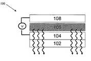
- FIG. 1shows a cross-sectional schematic diagram of a light strip in accordance with the present invention.
- FIG. 2shows a cross-sectional schematic diagram of a light strip based on an organic light emitting diode design.
- FIG. 3shows a cross-sectional schematic diagram of a light strip that uses an AC voltage source.
- FIG. 4shows an organic ligand-capped nanoparticle.
- FIG. 5shows a cross-sectional schematic diagram of a portion of a keypad backlit by a light strip in accordance with the present invention.
- FIG. 6shows a cross-sectional schematic diagram of a portion of a keypad having a light strip incorporated directly into a key.
- FIG. 7shows an embodiment of an electronic device having a lighted keypad.
- the present inventionprovides light strips for use as stand alone illumination sources and as illumination sources in a variety of electronic devices.
- the light stripsdesirably take on the form of a continuous thin film of light emitting material based on electroluminescent semiconductor nanoparticles.
- the light stripsmay take on a wide range of dimensions, including long narrow tapes or plates tailored to fit specific device applications.
- FIG. 1provides an exemplary embodiment of a light strip in accordance with the present invention.
- the light strip presented hereis a four-layered strip.
- 100represents the light strip comprising multiple layers in a generally laminar arrangement.
- 102represents a substrate layer that may provide a support, protective layer and/or electrical insulation layer.
- 104represents a first electrode layer. Layer 104 can be disposed on and generally laminar with the substrate layer 102 .
- 106represents a light-emitting layer comprising a plurality of electroluminescent semiconductor nanoparticles. Layer 106 may be made from a conductive binder if the light strip is to be used with a DC source or from a dielectric binder is the light strip is to be used with an AC source.
- Layer 106can be generally laminar with and disposed on the first electrode layer 104 .
- 108represents a second electrode layer, different from the first electrode layer.
- Layer 108can be generally laminar with and disposed on the light-emitting layer 106 .
- the second electrode layeris desirably made of a reflective material and helps to direct emitted photons out of the device.
- a second insulating layer(not shown) may be disposed over the second electrode layer.
- 108can be a cathode
- 104can be an anode.
- Cathodes and anodescan be multi-layered if desired such as, for example, a bi-layer cathode or a bi-layer anode.
- the first and second electrode layerscan sandwich the light-emitting layer 106 .
- the first electrode layer 104 and the substrate 102 layerare desirably substantially transparent such that when an electrical signal is applied across the first and second electrodes to induce the nanoparticles in the light emitting layer to electroluminesce, as least a portion of the emitted light passes through the two layers 102 and 104 .
- a substantially transparent layeris one that transmits enough light for a user to see, although some light may be absorbed or reflected.
- the light stripsmay have an organic light emitting diode (OLED) type structure, as shown in FIG. 2 .
- OLEDorganic light emitting diode
- the first electrode 202is a substantially transparent electrode, such as an indium tin oxide (ITO) thin film, optionally disposed atop a transparent substrate 206 .
- ITOindium tin oxide
- the OLED light stripincludes a hole-transport layer 208 , an electroluminescent light emitting layer 210 , and an electron-transport layer 209 . Both the electron transport layer and the hole transport layer may be made of a doped polymeric material, such as poly(phenylene vinylene).
- OLED structureOther layers that may optionally be incorporated into the OLED structure include, a hole injection layer, an electron injection layer and a hole blocking layer.
- a DC voltageis applied to the OLED, the injected positive and negative charges recombine in the electroluminescent emissive layer to create an illumination source.
- FIG. 3shows a cross-sectional view of a light strip designed for use with an AC source.
- electroluminescenceresults from electrons flowing within an insulated light emitting layer under the influence of an applied AC bias.
- the light stripis essentially a capacitor formed from a dielectric layer positioned between two conductive electrodes that emits light in the presence of a strong electric field, using very little current.
- the light strip 300 shown in FIG. 3includes a light emitting layer 302 disposed between a dielectric layer 304 and a substantially transparent electrode 306 .
- the light emitting layer 302comprises semiconductor nanoparticles dispersed in a dielectric medium.
- the light stripfurther includes a second electrode layer 308 disposed below the dielectric layer 304 and an insulating layer 310 disposed below the second electrode layer 308 .
- the thickness of the light stripis not particularly limited. However, the light strips desirably provide a low profile illumination source. In general, the light strips should be thin and robust enough to allow for rolling, handling, packaging, and facile attachment to a variety of substrates, including floors, walls, ceilings and shelves.
- the thicknesscan be, for example, about 100 nm to about 2 mm.
- the thicknesscan be, for example, about 25 nm to about 5 microns, or more particularly about 50 nm to about 1,000 nm, and more particularly, about 50 nm to about 200 nm.
- the anodemay be made of ITO, tin oxide, indium oxide, zinc oxide, indium zinc oxide, aluminum oxide, gold, silver, or composite coatings, such as metal nanocrystal coatings or carbon nanotube doped polymers.
- the anode materialswill be selected to provide the desired combination of electrical conductivity and optical transparency.
- Suitable cathode materialsinclude, for example, K, Li, Na, Mg, La, Ce, Ca, Sr, Ba, Al, Ag, In, Sn, Zn, Zr, or mixtures thereof.
- Preferred materials for the manufacture of cathodesinclude Ag—Mg, Al—Li, In—Mg, and Al—Ca alloys.
- Tris(8-hydroxyquinolato) aluminum(Alq3) may be used as an electron-transporting material.
- 3-phenyl-4-(1f-naphthyl)-5-phenyl-1,2,4-triazole(TAZ) may be used as a hole blocking material.
- N,N′-bis(3-methylphenyl)-N,N′-diphenylbenzidine(TPD) may be used as a hole transport material.
- PDApoly-3,4-ethylenedioxythiophene
- PEDOTis a conductive polymer that may be used as a hole injection material.
- nanoparticlegenerally refers to particles that have an average diameter between about 1 nm to 100 nm and may, in some instances, include elongated particle shapes, such as nanowires, in addition to more spherical, triangular or square particles. Nanoparticles have an intermediate size between individual atoms and macroscopic bulk solids. Nanoparticles may have a size on the order of the Bohr exciton radius (e.g. 4.9 nm for silicon), of the material or less, which allows individual nanoparticles to trap individual or discrete numbers of charge carriers, either electrons or holes, or excitons, within the particle.
- Bohr exciton radiuse.g. 4.9 nm for silicon
- the spatial confinement of electrons (or holes) by nanoparticlesis believed to alter the physical, optical, electronic, catalytic, optoelectronic and magnetic properties of the material.
- the alterations of the physical properties of a nanoparticle due to confinement of electronsare generally referred to as quantum confinement effects.
- Nanoparticlesmay exhibit a number of unique electronic, magnetic, catalytic, physical, optoelectronic and optical properties due to quantum confinement effects. For example, many nanoparticles exhibit photoluminescence or electroluminescence effects that are significantly greater than the photoluminescent or electroluminescence effects of macroscopic materials having the same composition. Additionally, these quantum confinement effects may vary as the size of the nanoparticle is varied.
- the nanoparticlesmay typically have at least one dimension, such as an average diameter, which is about 100 nm or less, more particularly about 50 nm or less, and still more particularly about 10 nm or less.
- the dimensioncan be about 0.5 nm to about 15 nm, or about 0.1 nm to about 10 nm.
- a collection of nanoparticlesmay be designed to include nanoparticles that emit light of different colors across the visible spectrum.
- the light stripsmay be designed to provide substantially monochromatic light, or polychromatic light with a selected color blend.
- the optimum size distribution of the nanoparticleswill depend on a variety of factors, including the voltage used to excite the nanoparticles, the composition of the nanoparticles, and the desired color and quality of the emitted light.
- the intensity and/or color of the light emitted along the length of the light stripmay be tailored for a desired application.
- the semiconductor nanoparticles used to produce the light stripsmay be made from variety of semiconductor materials including, but are not limited to, Group IV semiconductors and alloys of Group IV semiconductors, Group II-VI semiconductors, and Group III-V semiconductors.
- Group IV semiconductor nanoparticlesincluding silicon nanoparticles, germanium nanoparticles, and SiGe alloy nanoparticles, Si or Ge cores comprising an organic or inorganic coating, or nanoparticles doped with impurities are particularly well suited for use in the light strips described herein.
- the Group IV nanoparticlesmay be core/shell nanoparticles having a Si or Ge core coated with an inorganic shell.
- the inorganic shellis composed of a wider bandgap semiconductor, such as ZnS, SiC, Si 3 N 4 or CdS.
- the coree.g. Si
- the nanoparticlesmay be composed of a Si core and a Si 3 N 4 shell.
- Such core/shell nanoparticlesmay be made by adapting processes that have been used to produce larger core/shell particles or those used to produce core/shell nanoparticles for other material systems.
- the specific emission spectrum of each nanoparticle in a collection of electroluminescent semiconductor nanoparticlesis dependent upon the size of the nanoparticle.
- the particle size distribution of the nanoparticles in a given light stripwill vary somewhat depending on the intended application.
- the electroluminescent nanoparticlesmay desirably be surface treated with organic or inorganic passivating agents that prevent reactive degradation of the nanoparticles when exposed to water and oxygen or other chemical contaminants.
- organic passivating agentsor “capping agents”, are described in U.S. Patent Application No. 2003/0003300; Nano Letters, 2, 681-685 (2002); and J. Am. Chem. Soc., 123, 3743-3748 (2001), the entire disclosures of which are incorporated herein by reference.
- Other suitable passivating agents and their productionare described in J. M. Buriak, Chemical Reviews, 102(5), pp. 1271-1308 (2002).
- the light emitting layers in the light strips in accordance with the present inventionmay be composed of semiconductor nanoparticles coated on or embedded in materials acting as a support or binder for the nanoparticles.
- the support or binder materialmay have a lower refractive index than that of the nanoparticles.
- the support or binder materialis desirably substantially transparent to the emitted electroluminescence.
- the nanoparticlesare supported in a flexible polymer matrix.
- suitable support or binder materialsinclude any of various polymers such as polyvinylidene fluoride, polyethylene oxide, polyethylene, polypropylene, polytetrafluoroethylene, polyacrylates and mixtures and copolymers thereof.
- suitable polymer bindersinclude, but are not limited to, polystyrenes, polyimides, epoxies, acrylic polymers, polyurethanes and polycarbonates. Still other suitable binders are nitrocellulose, cyanoethyl cellulose and cyanoethyl pullulan. Alternatively, the nanoparticles may be coated with or embedded in an inorganic binder, such as silica glasses, silica gels or silicone polymers.
- the nanoparticlesmay be dispersed in a polymeric binder by mixing the nanoparticles, the binder and optionally an appropriate solvent and/or dispersants.
- Suitable solventsinclude high vapor pressure organic solvents, such as hexane, cyclohexane, toluene or xylene, which may be easily removed once the dispersion has been formed into a coating, film or layer.
- the mixturemay then be dried, hardened, cured or otherwise solidified to provide a dispersion of nanoparticles in a solid host matrix of binder.
- the bindertakes the form of polymerizable monomers or oligomers that are polymerized after mixing with the nanoparticles.
- An exemplary method for dispersing nanoparticles in a epoxy binderis described in U.S. Pat. No. 6,501,091, the entire disclosure of which is incorporated herein by reference.
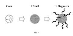
- small nanoparticlesincluding small core/shell nanoparticles, of the type that may be produced using organic capping agents as described in the above-cited references, are solution processable due to the presence of organic capping ligands attached to the outer surface of the nanoparticles.
- FIG. 4is an illustration of such ligand capped nanoparticles.
- These soluble nanoparticlesmay be made with sizes that enable them to easily pass through ink jet printing heads.
- a light emitting layermay be printed directly onto an underlying electrode or other substrate. This is advantageous because it allows for the design and fabrication of light emitting layers having specific color and/or intensity patterns.
- iteliminates the need for an inverter which is required in mobile devices using more conventional light sources. Inverters take up valuable device space, are expensive and detract from efficiency.
- all of the nanoparticles that make up the light emitting layer of a light stripmay be embedded in the polymer binder.
- nanoparticles that emit a single colori.e. a group of nanoparticles having a substantially monodisperse size distribution
- domains of red-emitting nanoparticles, domains of blue-emitting nanoparticles, and domains of green emitting nanoparticlesmay be present in different regions along the length of the light strip.
- the deposition of the domains on top of the bindermay be carried out by conventional screen printing or ink-jet printing techniques.
- monodisperse suspensions of nanoparticles representing different colorscould be placed in the different printing heads of an ink jet printer and printed directly to an organic film.
- Ink jet printingcan provide better control and higher throughput.
- Screen printingcan be used with higher viscosity solutions.
- screen printing of OLEDsis described in U.S. patent publication 2002/0167024, published Nov. 14, 2002, to Jabbour et al. Formation of thin film layers can be carried out by methods described in, for example, Marc J. Madou, Fundamentals of Microfabrication, The Science of Miniaturization, 2 nd Ed., 2002, Chapter 3.
- the organic film onto which the domains are printedmay also have a mono or polydisperse distribution of nanoparticles embedded within it.
- Two general approachesmay be used to produce nanoparticles having an appropriate size distribution.
- the reaction conditionsare carefully controlled during the production of the nanoparticles such that nanoparticles having a broad size distribution are produced in a single synthesis.
- batches of particles of a given sizeare produced separately and particles of the appropriate size are then selected and mixed together in the desired amounts.
- the nanoparticlesmay be produced in situ, as by conventional epitaxial growth processes.
- a core-shell structuremay be produced by first growing nanocrystals of a first semiconductor material, such as germanium, on a substrate, such as a silicon substrate, using well known lithographic techniques and subsequently growing an epitaxial layer of a second semiconductor material, such as silicon around the nanocrystals.
- a second semiconductor materialsuch as silicon around the nanocrystals.
- CVDchemical vapor deposition
- Silicon nanoparticlesmay also be formed using a deconstructive approach, such as by etching from a bulk silicon wafer, followed by ultrasonic exposure and separation of the nanoparticles by different sizes.
- Suitable etch-based methods for producing nanoparticlesmay be found in Properties of Porous Silicon, Leigh Canham Ed.; INSPEC (1997), ISBN 0852969325, pp. 3-29; Heinrich, et al., Science, 255, pp. 66-68 (1992); Belomoin, et al., Appl. Phys. Lett., 77(6), p. 779-781 (2000); and Belomoin, et al., Appl. Phys. Lett., 80(5), p. 841-843 (2002), the entire disclosures of which are incorporated herein by reference.
- Group IV nanowiresare described in, for example, the following publications, which are hereby incorporated by reference in their entirety: (a) Lu, Hanrath, Johnston, and Korgel, NanoLetters, 2003, Vol. 3, No. 1, pgs. 93-99 (“Growth of Single Crystal Silicon Nanowires in Supercritical Solution from Tethered Gold Particles on a Silicon Substrate”); (b) Holmes, Johnston, Doty, Korgel, Science, 287, Feb. 25, 2000, pages 1471-1473 (“Control of Thickness and Orientation of Solution-Grown Silicon Nanowires”); and (c) Hanrath, Korgel, J. Am. Chem. Soc., Vol. 124, No.
- nanoparticle size controlcan be obtained by controlling the synthesis conditions, such as reaction temperature, pressure, precursor concentration, flow rate, dilutant type, dilutant concentration, reagent type and reagent concentration. Because the particle size distribution can be controlled, the nanoparticles provide a single material solution for color tuning in the visible spectrum. Other noteworthy attributes of the particles may include one or more of the following: temperature and humidity independent emissions, high quantum efficiencies, use of a single material to reach the entire visible range, fast radiative rates, and, in the case of Si nanoparticles, a 1:1 lattice match with bulk silicon. With proper passivation, the nanoparticles can be stored on a shelf for years without degradation. The different size (color) particles also may not suffer from differential aging, allowing the devices to maintain constant color quality over time.
- Light strips made from the nanoparticlesare desirably, but not necessarily, thin, flexible laminar films and light emitting layers in the light strips are desirably, but not necessarily, continuous thin films, where “continuous” simply indicates that the light emitting layer is a single piece of material, although the density and size distribution of the nanoparticles in the film may be non-uniform.
- the thickness of the light emitting layer containing the semiconductor nanoparticles in the light stripsis not particularly limited but can be, for example, about 4 nm to about 1 mm, more particularly, about 50 nm to about 100 microns, and more particularly, about 100 nm to about 50 microns.
- the light emitting layercan be sufficiently thin to be a monolayer of nanoparticles, wherein the thickness of the material is approximately the diameter of the nanoparticle.
- the light stripsare well-suited for use as stand-alone illumination sources for accent lighting, path lighting and emergency lighting.
- the light stripsinclude a light emitting layer having a nanoparticle density gradient along its length. These light strips would emit a light of increasing intensity along one direction.
- This lighting designcould be useful, for example, to indicate the direction of a destination, such as an exit, where the light becomes more intense as the light strip approaches the destination.
- the light stripsmay include a light emitting layer having a plurality of regions along its length, wherein different regions have a different nanoparticle size distribution. These light strips would emit light of different colors from different regions along their length. This lighting design could be useful, for example, to highlight different sections or objects along a path.
- a walkway or aislecould be illuminated in one color while the periphery of a door way could be illuminated in a different color.
- the intensity and/or size distribution of nanoparticles in the light stripsmay be designed to provide an intensity and/or color pattern along the light strips for decorative purposes. Locations where the light strips may advantageously be used as stand alone illumination sources include airplanes, movie theaters and retail stores (e.g., to highlight displays) The light strips may also be used to provide low-level illumination for cupboards and shelves in bookcases, bars and the like.
- Another advantage to using a light emitting layer having a plurality of separate regions with different nanoparticle density distributionsis that if one region has a defect (e.g., a pin hole defect) that produces a short, that defect can be isolated to that region while other regions which are electrically isolated from the defective region remain unaffected.
- a defecte.g., a pin hole defect
- the light strips provided hereinare also well-suited for use as lighting in electronic devices.
- devices that may be lit by the present light stripsinclude, but are not limited to, cellular phones, personal digital assistants (PDAs), watches, personal computers and car audio components.
- PDAspersonal digital assistants
- the present light stripshave low power requirements, they are particularly suited for lighting in portable battery operated devices, such as PDAs and cellular phones where power usage directly affects battery life.
- the light stripsmay be used to backlight display screens and/or keypads. In such devices a display or a substantially transparent keypad would be placed in front of (i.e., in the light emission path of) a light strip.
- the lighted components of electronic devices, including the keys of a keypadmay directly incorporate the light strips into their structure, such that the components are themselves light-emitting.
- Liquid crystal displaysare an example of the type of display that may be lit with a light strip in accordance with the present invention.
- Electronic devices that include both a display and a keypadmay include a single light strip to illuminate both the display and the keypad.
- the light stripis used as a backlighting source the light strip would desirably have dimensions such that it fit beneath the face plate of the device. Because liquid crystal displays tend to absorb a lot of light (e.g., up to 90% of the backlight), it may be desirable to provide a light strip that emits a higher light intensity from the area behind the display screen and a lower light intensity from the area behind the keypad.
- a light strip with a light emitting layer having a first regioni.e., the region behind the keypad
- a second regioni.e., the region behind the keypad
- the light stripsmay be designed to illuminate different keys on a keypad with different colors of light.
- FIG. 5is a schematic cross-sectional view of a part of a keypad 500 that is backlit using a light strip in accordance with the present invention.
- the keypadincludes a protective faceplate 502 (optional) and at least one key 504 disposed below the faceplate.
- the faceplate 502 and keyare desirably made of a transparent material, such as a plastic.
- the light strip 506is disposed below the key 504 such that light emitted from the light strip 506 passes through the key 504 and the faceplate 502 .
- a voltagee.g., supplied from a battery in the device
- the light stripis disposed over a push-type switch 508 .
- the push-type switchcompletes a circuit in the electronic device when the at least one key 504 is pressed by a user.
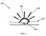
- FIG. 6is a schematic cross-sectional view of a part of a keypad 600 having a light strip incorporated into a key in accordance with the present invention.
- the keypadincludes a protective faceplate 602 (optional) and at least one key 604 disposed below the faceplate.
- the faceplate 602 and keyare desirably made of a transparent material, such as a plastic.
- a light strip 606is incorporated into the at least one key 604 .
- the light stripdefines the upper surface of the key.
- a voltagee.g., supplied from a battery in the device
- the light stripis disposed over a push-type switch 608 .
- the push-type switchcompletes a circuit in the electronic device when the at least one key 604 is pressed by a user.
- FIG. 7is a schematic illustration of an electronic device which can incorporate any of the disclosed light strips.
- the device 700has a keypad 704 having keys 708 and 710 .
- the devicealso includes a display 712 .
- the devicefurther includes any of the light strips disclosed herein.
- a single light stripis used to illuminate both the display and the keypad.
- the light stripis configured so that the display 712 is of a higher intensity and different color (bright white) than the keys 708 (blue) and 710 (dull white) of the keypad.
Landscapes
- Engineering & Computer Science (AREA)
- Chemical & Material Sciences (AREA)
- Nanotechnology (AREA)
- Physics & Mathematics (AREA)
- Crystallography & Structural Chemistry (AREA)
- Optics & Photonics (AREA)
- General Physics & Mathematics (AREA)
- Theoretical Computer Science (AREA)
- Materials Engineering (AREA)
- Condensed Matter Physics & Semiconductors (AREA)
- Life Sciences & Earth Sciences (AREA)
- Biophysics (AREA)
- Composite Materials (AREA)
- Inorganic Chemistry (AREA)
- Electroluminescent Light Sources (AREA)
Abstract
Description
Claims (15)
Priority Applications (1)
| Application Number | Priority Date | Filing Date | Title |
|---|---|---|---|
| US11/201,406US7750352B2 (en) | 2004-08-10 | 2005-08-10 | Light strips for lighting and backlighting applications |
Applications Claiming Priority (2)
| Application Number | Priority Date | Filing Date | Title |
|---|---|---|---|
| US60020104P | 2004-08-10 | 2004-08-10 | |
| US11/201,406US7750352B2 (en) | 2004-08-10 | 2005-08-10 | Light strips for lighting and backlighting applications |
Publications (2)
| Publication Number | Publication Date |
|---|---|
| US20060034065A1 US20060034065A1 (en) | 2006-02-16 |
| US7750352B2true US7750352B2 (en) | 2010-07-06 |
Family
ID=35799740
Family Applications (1)
| Application Number | Title | Priority Date | Filing Date |
|---|---|---|---|
| US11/201,406Expired - Fee RelatedUS7750352B2 (en) | 2004-08-10 | 2005-08-10 | Light strips for lighting and backlighting applications |
Country Status (1)
| Country | Link |
|---|---|
| US (1) | US7750352B2 (en) |
Cited By (17)
| Publication number | Priority date | Publication date | Assignee | Title |
|---|---|---|---|---|
| US20100300856A1 (en)* | 2009-06-01 | 2010-12-02 | Apple Inc. | White point adjustment for multicolor keyboard backlight |
| US20100301755A1 (en)* | 2009-06-01 | 2010-12-02 | Apple Inc. | Light source with light sensor |
| US20100306683A1 (en)* | 2009-06-01 | 2010-12-02 | Apple Inc. | User interface behaviors for input device with individually controlled illuminated input elements |
| US20100328935A1 (en)* | 2009-06-30 | 2010-12-30 | Apple Inc. | Multicolor lighting system |
| US8303151B2 (en) | 2010-05-12 | 2012-11-06 | Apple Inc. | Microperforation illumination |
| US8378857B2 (en) | 2010-07-19 | 2013-02-19 | Apple Inc. | Illumination of input device |
| US8378972B2 (en) | 2009-06-01 | 2013-02-19 | Apple Inc. | Keyboard with increased control of backlit keys |
| US20130088147A1 (en)* | 2011-10-11 | 2013-04-11 | Hyundai Motor Company | Organic electro-luminescence lighting device for vehicle |
| US8451146B2 (en) | 2010-06-11 | 2013-05-28 | Apple Inc. | Legend highlighting |
| US8969856B2 (en) | 2012-08-29 | 2015-03-03 | General Electric Company | OLED devices with internal outcoupling |
| US9275810B2 (en) | 2010-07-19 | 2016-03-01 | Apple Inc. | Keyboard illumination |
| US9431623B2 (en) | 2008-02-07 | 2016-08-30 | Qd Vision, Inc. | Flexible devices including semiconductor nanocrystals, arrays, and methods |
| US11139442B2 (en)* | 2019-03-12 | 2021-10-05 | Universal Display Corporation | Nanopatch antenna outcoupling structure for use in OLEDs |
| US20230006162A1 (en)* | 2019-12-09 | 2023-01-05 | Sharp Kabushiki Kaisha | Light emitting device, and method for manufacturing light emitting device |
| US11569480B2 (en) | 2019-03-12 | 2023-01-31 | Universal Display Corporation | Plasmonic OLEDs and vertical dipole emitters |
| US11637261B2 (en)* | 2019-03-12 | 2023-04-25 | Universal Display Corporation | Nanopatch antenna outcoupling structure for use in OLEDs |
| US12414433B2 (en) | 2022-02-11 | 2025-09-09 | Universal Display Corporation | Organic electroluminescent devices |
Families Citing this family (93)
| Publication number | Priority date | Publication date | Assignee | Title |
|---|---|---|---|---|
| JP2004294163A (en)* | 2003-03-26 | 2004-10-21 | Yazaki Corp | Dial for vehicle instrument, dial manufacturing method and dial manufacturing apparatus |
| US7335259B2 (en)* | 2003-07-08 | 2008-02-26 | Brian A. Korgel | Growth of single crystal nanowires |
| US8718437B2 (en)* | 2006-03-07 | 2014-05-06 | Qd Vision, Inc. | Compositions, optical component, system including an optical component, devices, and other products |
| WO2007103310A2 (en)* | 2006-03-07 | 2007-09-13 | Qd Vision, Inc. | An article including semiconductor nanocrystals |
| US9297092B2 (en) | 2005-06-05 | 2016-03-29 | Qd Vision, Inc. | Compositions, optical component, system including an optical component, devices, and other products |
| KR100700143B1 (en)* | 2005-12-02 | 2007-03-28 | 엘지전자 주식회사 | Key selection display device of touch keypad and method |
| US7547888B2 (en)* | 2005-12-21 | 2009-06-16 | Los Alamos National Security, Llc | Nanocomposite scintillator and detector |
| WO2007092606A2 (en)* | 2006-02-09 | 2007-08-16 | Qd Vision, Inc. | Displays including semiconductor nanocrystals and methods of making same |
| US9951438B2 (en) | 2006-03-07 | 2018-04-24 | Samsung Electronics Co., Ltd. | Compositions, optical component, system including an optical component, devices, and other products |
| US9874674B2 (en) | 2006-03-07 | 2018-01-23 | Samsung Electronics Co., Ltd. | Compositions, optical component, system including an optical component, devices, and other products |
| WO2007143197A2 (en) | 2006-06-02 | 2007-12-13 | Qd Vision, Inc. | Light-emitting devices and displays with improved performance |
| US8849087B2 (en)* | 2006-03-07 | 2014-09-30 | Qd Vision, Inc. | Compositions, optical component, system including an optical component, devices, and other products |
| WO2007120443A2 (en)* | 2006-03-27 | 2007-10-25 | Los Alamos National Security, Llc | Nanocomposite scintillator, detector, and method |
| WO2007117698A2 (en)* | 2006-04-07 | 2007-10-18 | Qd Vision, Inc. | Composition including material, methods of depositing material, articles including same and systems for depositing material |
| US9105776B2 (en)* | 2006-05-15 | 2015-08-11 | Stion Corporation | Method and structure for thin film photovoltaic materials using semiconductor materials |
| US8017860B2 (en)* | 2006-05-15 | 2011-09-13 | Stion Corporation | Method and structure for thin film photovoltaic materials using bulk semiconductor materials |
| US8941299B2 (en)* | 2006-05-21 | 2015-01-27 | Massachusetts Institute Of Technology | Light emitting device including semiconductor nanocrystals |
| JP2010508620A (en)* | 2006-09-12 | 2010-03-18 | キユーデイー・ビジヨン・インコーポレーテツド | Electroluminescent display useful for displaying a predetermined pattern |
| WO2008063657A2 (en)* | 2006-11-21 | 2008-05-29 | Qd Vision, Inc. | Light emitting devices and displays with improved performance |
| US8836212B2 (en)* | 2007-01-11 | 2014-09-16 | Qd Vision, Inc. | Light emissive printed article printed with quantum dot ink |
| US20080300918A1 (en)* | 2007-05-29 | 2008-12-04 | Commercenet Consortium, Inc. | System and method for facilitating hospital scheduling and support |
| WO2009014590A2 (en) | 2007-06-25 | 2009-01-29 | Qd Vision, Inc. | Compositions and methods including depositing nanomaterial |
| US9136498B2 (en) | 2007-06-27 | 2015-09-15 | Qd Vision, Inc. | Apparatus and method for modulating photon output of a quantum dot light emitting device |
| US8071179B2 (en) | 2007-06-29 | 2011-12-06 | Stion Corporation | Methods for infusing one or more materials into nano-voids if nanoporous or nanostructured materials |
| US7919400B2 (en)* | 2007-07-10 | 2011-04-05 | Stion Corporation | Methods for doping nanostructured materials and nanostructured thin films |
| WO2009014707A2 (en) | 2007-07-23 | 2009-01-29 | Qd Vision, Inc. | Quantum dot light enhancement substrate and lighting device including same |
| US8743077B1 (en)* | 2007-08-01 | 2014-06-03 | Sipix Imaging, Inc. | Front light system for reflective displays |
| US8128249B2 (en)* | 2007-08-28 | 2012-03-06 | Qd Vision, Inc. | Apparatus for selectively backlighting a material |
| US8759671B2 (en)* | 2007-09-28 | 2014-06-24 | Stion Corporation | Thin film metal oxide bearing semiconductor material for single junction solar cell devices |
| US8614396B2 (en)* | 2007-09-28 | 2013-12-24 | Stion Corporation | Method and material for purifying iron disilicide for photovoltaic application |
| US8058092B2 (en)* | 2007-09-28 | 2011-11-15 | Stion Corporation | Method and material for processing iron disilicide for photovoltaic application |
| US8287942B1 (en) | 2007-09-28 | 2012-10-16 | Stion Corporation | Method for manufacture of semiconductor bearing thin film material |
| US7998762B1 (en) | 2007-11-14 | 2011-08-16 | Stion Corporation | Method and system for large scale manufacture of thin film photovoltaic devices using multi-chamber configuration |
| US8440903B1 (en) | 2008-02-21 | 2013-05-14 | Stion Corporation | Method and structure for forming module using a powder coating and thermal treatment process |
| US8075723B1 (en) | 2008-03-03 | 2011-12-13 | Stion Corporation | Laser separation method for manufacture of unit cells for thin film photovoltaic materials |
| US8772078B1 (en) | 2008-03-03 | 2014-07-08 | Stion Corporation | Method and system for laser separation for exclusion region of multi-junction photovoltaic materials |
| KR20110008206A (en) | 2008-04-03 | 2011-01-26 | 큐디 비젼, 인크. | Light Emitting Device Including Quantum Dots |
| US9525148B2 (en) | 2008-04-03 | 2016-12-20 | Qd Vision, Inc. | Device including quantum dots |
| US9207385B2 (en) | 2008-05-06 | 2015-12-08 | Qd Vision, Inc. | Lighting systems and devices including same |
| WO2009151515A1 (en) | 2008-05-06 | 2009-12-17 | Qd Vision, Inc. | Solid state lighting devices including quantum confined semiconductor nanoparticles |
| WO2009137053A1 (en) | 2008-05-06 | 2009-11-12 | Qd Vision, Inc. | Optical components, systems including an optical component, and devices |
| US7939454B1 (en) | 2008-05-31 | 2011-05-10 | Stion Corporation | Module and lamination process for multijunction cells |
| US8642138B2 (en) | 2008-06-11 | 2014-02-04 | Stion Corporation | Processing method for cleaning sulfur entities of contact regions |
| US9087943B2 (en)* | 2008-06-25 | 2015-07-21 | Stion Corporation | High efficiency photovoltaic cell and manufacturing method free of metal disulfide barrier material |
| US8003432B2 (en) | 2008-06-25 | 2011-08-23 | Stion Corporation | Consumable adhesive layer for thin film photovoltaic material |
| US8207008B1 (en) | 2008-08-01 | 2012-06-26 | Stion Corporation | Affixing method and solar decal device using a thin film photovoltaic |
| US7855089B2 (en)* | 2008-09-10 | 2010-12-21 | Stion Corporation | Application specific solar cell and method for manufacture using thin film photovoltaic materials |
| US8008112B1 (en) | 2008-09-29 | 2011-08-30 | Stion Corporation | Bulk chloride species treatment of thin film photovoltaic cell and manufacturing method |
| US8476104B1 (en) | 2008-09-29 | 2013-07-02 | Stion Corporation | Sodium species surface treatment of thin film photovoltaic cell and manufacturing method |
| US8394662B1 (en) | 2008-09-29 | 2013-03-12 | Stion Corporation | Chloride species surface treatment of thin film photovoltaic cell and manufacturing method |
| US8236597B1 (en) | 2008-09-29 | 2012-08-07 | Stion Corporation | Bulk metal species treatment of thin film photovoltaic cell and manufacturing method |
| US8501521B1 (en) | 2008-09-29 | 2013-08-06 | Stion Corporation | Copper species surface treatment of thin film photovoltaic cell and manufacturing method |
| US8008110B1 (en) | 2008-09-29 | 2011-08-30 | Stion Corporation | Bulk sodium species treatment of thin film photovoltaic cell and manufacturing method |
| US8026122B1 (en) | 2008-09-29 | 2011-09-27 | Stion Corporation | Metal species surface treatment of thin film photovoltaic cell and manufacturing method |
| US8425739B1 (en) | 2008-09-30 | 2013-04-23 | Stion Corporation | In chamber sodium doping process and system for large scale cigs based thin film photovoltaic materials |
| US7947524B2 (en)* | 2008-09-30 | 2011-05-24 | Stion Corporation | Humidity control and method for thin film photovoltaic materials |
| US7863074B2 (en)* | 2008-09-30 | 2011-01-04 | Stion Corporation | Patterning electrode materials free from berm structures for thin film photovoltaic cells |
| US8383450B2 (en)* | 2008-09-30 | 2013-02-26 | Stion Corporation | Large scale chemical bath system and method for cadmium sulfide processing of thin film photovoltaic materials |
| US7910399B1 (en) | 2008-09-30 | 2011-03-22 | Stion Corporation | Thermal management and method for large scale processing of CIS and/or CIGS based thin films overlying glass substrates |
| US8741689B2 (en)* | 2008-10-01 | 2014-06-03 | Stion Corporation | Thermal pre-treatment process for soda lime glass substrate for thin film photovoltaic materials |
| US20110018103A1 (en) | 2008-10-02 | 2011-01-27 | Stion Corporation | System and method for transferring substrates in large scale processing of cigs and/or cis devices |
| US8435826B1 (en) | 2008-10-06 | 2013-05-07 | Stion Corporation | Bulk sulfide species treatment of thin film photovoltaic cell and manufacturing method |
| US8003430B1 (en) | 2008-10-06 | 2011-08-23 | Stion Corporation | Sulfide species treatment of thin film photovoltaic cell and manufacturing method |
| USD625695S1 (en) | 2008-10-14 | 2010-10-19 | Stion Corporation | Patterned thin film photovoltaic module |
| US8168463B2 (en) | 2008-10-17 | 2012-05-01 | Stion Corporation | Zinc oxide film method and structure for CIGS cell |
| US8344243B2 (en)* | 2008-11-20 | 2013-01-01 | Stion Corporation | Method and structure for thin film photovoltaic cell using similar material junction |
| CN101545624A (en)* | 2009-05-08 | 2009-09-30 | 鲁意 | Illumination battery |
| USD662040S1 (en) | 2009-06-12 | 2012-06-19 | Stion Corporation | Pin striped thin film solar module for garden lamp |
| USD628332S1 (en) | 2009-06-12 | 2010-11-30 | Stion Corporation | Pin striped thin film solar module for street lamp |
| USD632415S1 (en) | 2009-06-13 | 2011-02-08 | Stion Corporation | Pin striped thin film solar module for cluster lamp |
| USD662041S1 (en) | 2009-06-23 | 2012-06-19 | Stion Corporation | Pin striped thin film solar module for laptop personal computer |
| USD652262S1 (en) | 2009-06-23 | 2012-01-17 | Stion Corporation | Pin striped thin film solar module for cooler |
| US8507786B1 (en) | 2009-06-27 | 2013-08-13 | Stion Corporation | Manufacturing method for patterning CIGS/CIS solar cells |
| USD627696S1 (en) | 2009-07-01 | 2010-11-23 | Stion Corporation | Pin striped thin film solar module for recreational vehicle |
| CN102598313B (en) | 2009-08-14 | 2016-03-23 | Qd视光有限公司 | Light emitting device, optical element for light emitting device, and method |
| US8398772B1 (en) | 2009-08-18 | 2013-03-19 | Stion Corporation | Method and structure for processing thin film PV cells with improved temperature uniformity |
| WO2011024020A1 (en)* | 2009-08-24 | 2011-03-03 | Certainteed Corporation | Thin films including nanoparticles with solar reflectance properties for building materials |
| WO2011047385A1 (en) | 2009-10-17 | 2011-04-21 | Qd Vision, Inc. | An optical, component, products including same, and methods for making same |
| US8809096B1 (en) | 2009-10-22 | 2014-08-19 | Stion Corporation | Bell jar extraction tool method and apparatus for thin film photovoltaic materials |
| US8859880B2 (en) | 2010-01-22 | 2014-10-14 | Stion Corporation | Method and structure for tiling industrial thin-film solar devices |
| US8263494B2 (en) | 2010-01-25 | 2012-09-11 | Stion Corporation | Method for improved patterning accuracy for thin film photovoltaic panels |
| US9096930B2 (en) | 2010-03-29 | 2015-08-04 | Stion Corporation | Apparatus for manufacturing thin film photovoltaic devices |
| US8461061B2 (en) | 2010-07-23 | 2013-06-11 | Stion Corporation | Quartz boat method and apparatus for thin film thermal treatment |
| SE535087C2 (en) | 2010-08-24 | 2012-04-10 | A method of preparing a flat surface with a controlled density gradient of deposited nanoparticle particles | |
| US8628997B2 (en) | 2010-10-01 | 2014-01-14 | Stion Corporation | Method and device for cadmium-free solar cells |
| CN102447070B (en)* | 2010-10-09 | 2014-05-14 | 中国计量学院 | Quantum-dot OLED (Organic Light Emitting Diode) light emitting device of photonic crystal structure |
| CN102456839A (en)* | 2010-10-21 | 2012-05-16 | 海洋王照明科技股份有限公司 | Organic electroluminescent device and preparation method thereof |
| US8728200B1 (en) | 2011-01-14 | 2014-05-20 | Stion Corporation | Method and system for recycling processing gas for selenization of thin film photovoltaic materials |
| US8998606B2 (en) | 2011-01-14 | 2015-04-07 | Stion Corporation | Apparatus and method utilizing forced convection for uniform thermal treatment of thin film devices |
| US8802486B2 (en)* | 2011-04-25 | 2014-08-12 | Sunpower Corporation | Method of forming emitters for a back-contact solar cell |
| US8436445B2 (en) | 2011-08-15 | 2013-05-07 | Stion Corporation | Method of manufacture of sodium doped CIGS/CIGSS absorber layers for high efficiency photovoltaic devices |
| US9929325B2 (en) | 2012-06-05 | 2018-03-27 | Samsung Electronics Co., Ltd. | Lighting device including quantum dots |
| US20220052284A1 (en)* | 2018-12-17 | 2022-02-17 | Sharp Kabushiki Kaisha | Electroluminescence element and display device |
Citations (132)
| Publication number | Priority date | Publication date | Assignee | Title |
|---|---|---|---|---|
| US3842306A (en) | 1973-06-21 | 1974-10-15 | Gen Electric | Alumina coatings for an electric lamp |
| US4047069A (en) | 1974-06-21 | 1977-09-06 | Matsushita Electronics Corporation | High-pressure mercury-vapor lamp having a plural phosphor coating |
| US4159443A (en) | 1978-07-18 | 1979-06-26 | Bell Telephone Laboratories, Incorporated | Electroluminescent optical devices |
| US4330691A (en) | 1980-01-31 | 1982-05-18 | The Futures Group, Inc. | Integral ceiling tile-loudspeaker system |
| US4642951A (en) | 1984-12-04 | 1987-02-17 | Fam Tile Restoration Services, Ltd. | Suspended ceiling tile system |
| US4890033A (en) | 1987-06-29 | 1989-12-26 | Nichia Kagaku Kogyo K.K. | Light-emitting composition and fluorescent lamp |
| US4923032A (en) | 1989-07-21 | 1990-05-08 | Nuernberger Mark A | Ceiling panel sound system |
| US4965485A (en) | 1988-02-10 | 1990-10-23 | Kabushiki Kaisha Toshiba | Halogen lamp envelope with roughened surface area and optical film |
| US5073805A (en) | 1989-02-06 | 1991-12-17 | Optoelectronics Technology Research Corporation | Semiconductor light emitting device including a hole barrier contiguous to an active layer |
| US5142343A (en) | 1989-08-18 | 1992-08-25 | Idemitsu Kosan Co., Ltd. | Organic electroluminescence device with oligomers |
| US5293050A (en) | 1993-03-25 | 1994-03-08 | International Business Machines Corporation | Semiconductor quantum dot light emitting/detecting devices |
| US5391088A (en)* | 1993-02-24 | 1995-02-21 | The Whitaker Corporation | Surface mount coupling connector |
| US5422489A (en) | 1994-01-24 | 1995-06-06 | Bhargava; Rameshwar N. | Light emitting device |
| US5438234A (en) | 1991-08-13 | 1995-08-01 | Kasei Optonix, Ltd. | Fluorescent lamp |
| US5516577A (en) | 1992-05-11 | 1996-05-14 | Idemitsu Kosan Co., Ltd. | Organic electroluminescence device |
| US5537000A (en) | 1994-04-29 | 1996-07-16 | The Regents, University Of California | Electroluminescent devices formed using semiconductor nanocrystals as an electron transport media and method of making such electroluminescent devices |
| US5536949A (en) | 1992-08-28 | 1996-07-16 | Idemistu Kosan Co., Ltd. | Charge injection auxiliary material and organic electroluminescence device containing the same |
| US5552665A (en) | 1994-12-29 | 1996-09-03 | Philips Electronics North America Corporation | Electric lamp having an undercoat for increasing the light output of a luminescent layer |
| US5796509A (en) | 1996-08-21 | 1998-08-18 | International Business Machines Corporation | Thin film frontlighting and backlighting for spatial light modulators |
| US5813753A (en) | 1997-05-27 | 1998-09-29 | Philips Electronics North America Corporation | UV/blue led-phosphor device with efficient conversion of UV/blues light to visible light |
| US5850064A (en) | 1997-04-11 | 1998-12-15 | Starfire Electronics Development & Marketing, Ltd. | Method for photolytic liquid phase synthesis of silicon and germanium nanocrystalline materials |
| US5852346A (en) | 1994-03-24 | 1998-12-22 | University Of Surrey | Forming luminescent silicon material and electro-luminescent device containing that material |
| US5882779A (en) | 1994-11-08 | 1999-03-16 | Spectra Science Corporation | Semiconductor nanocrystal display materials and display apparatus employing same |
| US5927845A (en) | 1995-08-28 | 1999-07-27 | Stantech | Integrally formed linear light strip with light emitting diodes |
| US5959316A (en) | 1998-09-01 | 1999-09-28 | Hewlett-Packard Company | Multiple encapsulation of phosphor-LED devices |
| US5960942A (en) | 1998-07-08 | 1999-10-05 | Ericsson, Inc. | Thin profile keypad with integrated LEDs |
| US5962863A (en) | 1993-09-09 | 1999-10-05 | The United States Of America As Represented By The Secretary Of The Navy | Laterally disposed nanostructures of silicon on an insulating substrate |
| US5977565A (en) | 1996-09-09 | 1999-11-02 | Kabushiki Kaisha Toshiba | Semiconductor light emitting diode having a capacitor |
| US5990479A (en) | 1997-11-25 | 1999-11-23 | Regents Of The University Of California | Organo Luminescent semiconductor nanocrystal probes for biological applications and process for making and using such probes |
| US6023371A (en) | 1997-06-09 | 2000-02-08 | Tdk Corporation | Color conversion material, and organic electroluminescent color display using the same |
| US6049090A (en)* | 1997-02-10 | 2000-04-11 | Massachusetts Institute Of Technology | Semiconductor particle electroluminescent display |
| US6069440A (en) | 1996-07-29 | 2000-05-30 | Nichia Kagaku Kogyo Kabushiki Kaisha | Light emitting device having a nitride compound semiconductor and a phosphor containing a garnet fluorescent material |
| US6068907A (en) | 1997-12-24 | 2000-05-30 | Arcoplast, Inc. | Closed edge fiberglass ceiling panels |
| US6117514A (en) | 1999-05-13 | 2000-09-12 | Herrmann; Richard J. | Ceiling tile system |
| JP2000285760A (en)* | 1999-03-31 | 2000-10-13 | Polymatech Co Ltd | Lighting sheet-like key top |
| US6157047A (en) | 1997-08-29 | 2000-12-05 | Kabushiki Kaisha Toshiba | Light emitting semiconductor device using nanocrystals |
| US6159620A (en)* | 1997-03-31 | 2000-12-12 | The Regents Of The University Of California | Single-electron solid state electronic device |
| US6169359B1 (en) | 1998-09-14 | 2001-01-02 | Planar Systems, Inc. | Electroluminescent phosphor thin films with increased brightness that includes an alkali halide |
| US6175187B1 (en) | 1998-02-12 | 2001-01-16 | Toshiba Lighting & Technology Corp. | Dual tube fluorescent lamp and light device |
| US6207229B1 (en) | 1997-11-13 | 2001-03-27 | Massachusetts Institute Of Technology | Highly luminescent color-selective materials and method of making thereof |
| US6215881B1 (en) | 1995-09-02 | 2001-04-10 | New Transducers Limited | Ceiling tile loudspeaker |
| US20010000622A1 (en) | 1996-06-26 | 2001-05-03 | Osram Opto Semiconductors Gmbh & Co., Ohg | Light-radiating semiconductor component with a luminescence conversion element |
| US6245259B1 (en) | 1996-09-20 | 2001-06-12 | Osram Opto Semiconductors, Gmbh & Co. Ohg | Wavelength-converting casting composition and light-emitting semiconductor component |
| US6252254B1 (en) | 1998-02-06 | 2001-06-26 | General Electric Company | Light emitting device with phosphor composition |
| US6252356B1 (en) | 1998-10-28 | 2001-06-26 | Matsushita Electric Industrial Co., Ltd. | Dispersed multicolor electroluminescent lamp and electroluminescent lamp unit employing thereof |
| US6251303B1 (en) | 1998-09-18 | 2001-06-26 | Massachusetts Institute Of Technology | Water-soluble fluorescent nanocrystals |
| US6252915B1 (en) | 1998-09-09 | 2001-06-26 | Qualcomm Incorporated | System and method for gaining control of individual narrowband channels using a wideband power measurement |
| EP1111966A2 (en) | 1999-12-22 | 2001-06-27 | General Electric Company | Luminescent display and method of making |
| US20010009351A1 (en) | 1999-04-30 | 2001-07-26 | Idemitsu Kosan Co., Ltd. | Organic electroluminescence element and manufacturing method thereof |
| US6283612B1 (en) | 2000-03-13 | 2001-09-04 | Mark A. Hunter | Light emitting diode light strip |
| US6310609B1 (en)* | 1997-04-17 | 2001-10-30 | Nokia Mobile Phones Limited | User interface with guide lights |
| US6336837B1 (en) | 1997-07-30 | 2002-01-08 | Matsushita Electric Industrial Co., Ltd. | Tungsten halogen lamp and method for manufacturing the same |
| US20020004251A1 (en) | 1999-03-15 | 2002-01-10 | Roberts John K. | Method of making a semiconductor radiation emitter package |
| US20020018632A1 (en) | 2000-03-06 | 2002-02-14 | Pelka David G. | Lighting apparatus having quantum dot layer |
| US20020025391A1 (en) | 1989-05-26 | 2002-02-28 | Marie Angelopoulos | Patterns of electrically conducting polymers and their application as electrodes or electrical contacts |
| US20020045276A1 (en)* | 1996-04-25 | 2002-04-18 | Juan Yguerabide | Analyte assay using particulate labels |
| US20020050975A1 (en)* | 2000-09-09 | 2002-05-02 | International Business Machines Corporation | Keyboard illumination for computing devices having backlit displays |
| US6389771B1 (en) | 2000-05-09 | 2002-05-21 | Ecophon Ab | Ceiling tile |
| US6397531B1 (en) | 2000-09-25 | 2002-06-04 | Daniel R. Martin | Ceiling display system |
| US6406803B1 (en) | 1997-05-19 | 2002-06-18 | 3M Innovative Properties Company | Electroluminescent device and method for producing the same |
| US6417019B1 (en) | 2001-04-04 | 2002-07-09 | Lumileds Lighting, U.S., Llc | Phosphor converted light emitting diode |
| US6441551B1 (en) | 1997-07-14 | 2002-08-27 | 3M Innovative Properties Company | Electroluminescent device and apparatus |
| US20020152704A1 (en) | 2001-02-15 | 2002-10-24 | Thompson Eugene W. | Ceiling panel and support system |
| US20020153830A1 (en) | 2001-02-07 | 2002-10-24 | Hieronymus Andriessen | Manufacturing of a thin film inorganic light emitting diode |
| US20020167024A1 (en) | 2001-03-30 | 2002-11-14 | The Arizona Board Of Regents | Method for fabricating organic light-emitting diode and organic light-emitting display using screen -printing |
| US20020183098A1 (en)* | 2001-04-20 | 2002-12-05 | Yung-Tang Lee | Cellular phone with caller ID light arrangement |
| US20020186921A1 (en)* | 2001-06-06 | 2002-12-12 | Schumacher Lynn C. | Multiwavelength optical fiber devices |
| US6501102B2 (en) | 1999-09-27 | 2002-12-31 | Lumileds Lighting, U.S., Llc | Light emitting diode (LED) device that produces white light by performing phosphor conversion on all of the primary radiation emitted by the light emitting structure of the LED device |
| US6501091B1 (en) | 1998-04-01 | 2002-12-31 | Massachusetts Institute Of Technology | Quantum dot white and colored light emitting diodes |
| US20030003300A1 (en)* | 2001-07-02 | 2003-01-02 | Korgel Brian A. | Light-emitting nanoparticles and method of making same |
| US20030003614A1 (en) | 2001-02-07 | 2003-01-02 | Hieronymus Andriessen | Manufacturing of a thin film inorganic light emitting diode |
| US6504179B1 (en) | 2000-05-29 | 2003-01-07 | Patent-Treuhand-Gesellschaft Fur Elektrische Gluhlampen Mbh | Led-based white-emitting illumination unit |
| US6508573B1 (en) | 1999-10-06 | 2003-01-21 | Ushiodenki Kabushiki Kaisha | Incandescent lamp |
| US6515314B1 (en)* | 2000-11-16 | 2003-02-04 | General Electric Company | Light-emitting device with organic layer doped with photoluminescent material |
| US6522065B1 (en) | 2000-03-27 | 2003-02-18 | General Electric Company | Single phosphor for creating white light with high luminosity and high CRI in a UV led device |
| US6521915B2 (en) | 2000-03-14 | 2003-02-18 | Asahi Rubber Inc. | Light-emitting diode device |
| US20030034486A1 (en) | 2001-07-02 | 2003-02-20 | Korgel Brian A. | Applications of light-emitting nanoparticles |
| US6526213B1 (en) | 1998-05-22 | 2003-02-25 | Fiberstars Incorporated | Light pipe composition |
| US20030042850A1 (en) | 2001-09-04 | 2003-03-06 | Dietrich Bertram | Electroluminescent device comprising quantum dots |
| US20030047816A1 (en) | 2001-09-05 | 2003-03-13 | Rensselaer Polytechnic Institute | Passivated nanoparticles, method of fabrication thereof, and devices incorporating nanoparticles |
| US20030057821A1 (en) | 2001-09-26 | 2003-03-27 | Si Diamond Technology, Inc. | Nanoparticle phosphor |
| US6544870B2 (en) | 2001-04-18 | 2003-04-08 | Kwangju Institute Of Science And Technology | Silicon nitride film comprising amorphous silicon quantum dots embedded therein, its fabrication method and light-emitting device using the same |
| US20030066998A1 (en) | 2001-08-02 | 2003-04-10 | Lee Howard Wing Hoon | Quantum dots of Group IV semiconductor materials |
| US20030080677A1 (en) | 2001-06-26 | 2003-05-01 | Mikhael Michael G. | Self-healing flexible photonic composites for light sources |
| US6585947B1 (en) | 1999-10-22 | 2003-07-01 | The Board Of Trustess Of The University Of Illinois | Method for producing silicon nanoparticles |
| US6602671B1 (en)* | 1998-09-18 | 2003-08-05 | Massachusetts Institute Of Technology | Semiconductor nanocrystals for inventory control |
| US6608330B1 (en) | 1998-09-21 | 2003-08-19 | Nichia Corporation | Light emitting device |
| US20030173541A1 (en) | 2001-07-30 | 2003-09-18 | Xiaogang Peng | Colloidal nanocrystals with high photoluminescence quantum yields and methods of preparing the same |
| US20030186023A1 (en) | 2002-03-26 | 2003-10-02 | Fuji Photo Film Co., Ltd | Process for preparing radiation image storage panel by gas phase deposition |
| US6632694B2 (en) | 2001-10-17 | 2003-10-14 | Astralux, Inc. | Double heterojunction light emitting diodes and laser diodes having quantum dot silicon light emitters |
| US6649138B2 (en) | 2000-10-13 | 2003-11-18 | Quantum Dot Corporation | Surface-modified semiconductive and metallic nanoparticles having enhanced dispersibility in aqueous media |
| US20030222572A1 (en) | 2002-05-28 | 2003-12-04 | National Taiwan University | Light emitting diode with nanoparticles |
| US6660410B2 (en) | 2000-03-27 | 2003-12-09 | Idemitsu Kosan Co., Ltd. | Organic electroluminescence element |
| US6661029B1 (en) | 2000-03-31 | 2003-12-09 | General Electric Company | Color tunable organic electroluminescent light source |
| US20030227249A1 (en) | 2002-06-07 | 2003-12-11 | Lumileds Lighting, U.S., Llc | Light-emitting devices utilizing nanoparticles |
| US6669158B2 (en) | 2002-04-26 | 2003-12-30 | Fernando R. Masas | Methods and apparatus for suspending fixtures |
| US20040007169A1 (en) | 2002-01-28 | 2004-01-15 | Mitsubishi Chemical Corporation | Semiconductor nanoparticles and thin film containing the same |
| US20040018382A1 (en) | 2002-07-29 | 2004-01-29 | Crosslink Polymer Research | Electroluminescent device and methods for its production and use |
| US20040023010A1 (en) | 2002-03-29 | 2004-02-05 | Vladimir Bulovic | Light emitting device including semiconductor nanocrystals |
| US20040027062A1 (en) | 2001-01-16 | 2004-02-12 | General Electric Company | Organic electroluminescent device with a ceramic output coupler and method of making the same |
| US6692512B2 (en) | 1998-10-13 | 2004-02-17 | Edwards Lifesciences Corporation | Percutaneous filtration catheter for valve repair surgery and methods of use |
| US6692986B1 (en) | 1999-09-09 | 2004-02-17 | Osram Opto Semiconductors Gmbh | Method for encapsulating components |
| US6693512B1 (en) | 2000-07-17 | 2004-02-17 | Armstrong World Industries, Inc. | Device location and identification system |
| US20040032214A1 (en) | 2001-08-17 | 2004-02-19 | Lee Sung Soo | White light-emitting organic electroluminescent element for back light and liquid crystal display device using the same |
| US20040033345A1 (en) | 2002-08-15 | 2004-02-19 | Benoit Dubertret | Water soluble metal and semiconductor nanoparticle complexes |
| US20040031966A1 (en) | 2002-08-16 | 2004-02-19 | Forrest Stephen R. | Organic photonic integrated circuit using a photodetector and a transparent organic light emitting device |
| US20040036130A1 (en) | 2001-08-02 | 2004-02-26 | Lee Howard Wing Hoon | Methods of forming quantum dots of group iv semiconductor materials |
| US6700322B1 (en) | 2000-01-27 | 2004-03-02 | General Electric Company | Light source with organic layer and photoluminescent layer |
| US6698543B2 (en) | 2001-07-03 | 2004-03-02 | Golterman & Sabo, Inc. | Acoustical wall panels |
| US6701686B1 (en) | 2003-01-16 | 2004-03-09 | Worthington Armstrong Venture | Ceiling grid with seal |
| US6702958B2 (en) | 2000-12-07 | 2004-03-09 | Kabushiki Kaisha Toshiba | Electroluminescent phosphor and electroluminescent element therewith |
| US6703781B2 (en) | 2002-05-21 | 2004-03-09 | Durel Corporation | El lamp with light scattering particles in cascading layer |
| US6733147B2 (en) | 2000-09-07 | 2004-05-11 | San Zhuang Wang | Backlighting system for displays |
| US20040105980A1 (en) | 2002-11-25 | 2004-06-03 | Sudarshan Tirumalai S. | Multifunctional particulate material, fluid, and composition |
| US6747402B2 (en)* | 2001-04-03 | 2004-06-08 | Matsushita Electric Industrial Co., Ltd. | EL element lighting unit employing the same EL element |
| US20040109666A1 (en) | 2002-12-10 | 2004-06-10 | John Kim | Optoelectronic devices employing fibers for light collection and emission |
| US20040126582A1 (en)* | 2002-08-23 | 2004-07-01 | Nano-Proprietary, Inc. | Silicon nanoparticles embedded in polymer matrix |
| US20040124352A1 (en) | 2002-12-27 | 2004-07-01 | Hideo Kashima | Method and apparatus for detecting dangerous substance |
| US20040145307A1 (en) | 2003-01-28 | 2004-07-29 | Kabushiki Kaisha Fine Rubber Kenkyuusho | Red light emitting phosphor, its production and light emitting device |
| US6787990B2 (en)* | 2002-05-28 | 2004-09-07 | Eastman Kodak Company | OLED area illumination light source having flexible substrate on a support |
| US6796624B2 (en)* | 2001-10-02 | 2004-09-28 | Hyuk Koo Park | Multifunction bookshelf |
| US6815064B2 (en)* | 2001-07-20 | 2004-11-09 | Quantum Dot Corporation | Luminescent nanoparticles and methods for their preparation |
| US20040245912A1 (en) | 2003-04-01 | 2004-12-09 | Innovalight | Phosphor materials and illumination devices made therefrom |
| US20040252488A1 (en) | 2003-04-01 | 2004-12-16 | Innovalight | Light-emitting ceiling tile |
| US6837604B2 (en)* | 2001-08-24 | 2005-01-04 | Matsushita Electric Industrial Co., Ltd. | Lighting apparatus |
| US6853132B2 (en)* | 2001-03-23 | 2005-02-08 | Seiko Epson Corporation | EL element, EL display, and electronic apparatus |
| US6936783B2 (en)* | 2001-05-25 | 2005-08-30 | Shin-Etsu Polymer Co., Ltd. | Push-button switch member and manufacturing method of same |
| US6956561B2 (en)* | 2001-09-04 | 2005-10-18 | Lg Electronics Inc. | Keypad backlighting of mobile terminal |
| US6959208B2 (en)* | 2001-10-16 | 2005-10-25 | Fujitsu Limited | Portable terminal |
| US20050236556A1 (en)* | 2004-04-19 | 2005-10-27 | Edward Sargent | Optically-regulated optical emission using colloidal quantum dot nanocrystals |
| US20060068154A1 (en)* | 2004-01-15 | 2006-03-30 | Nanosys, Inc. | Nanocrystal doped matrixes |
| US20080160733A1 (en) | 2007-01-03 | 2008-07-03 | Henry Hieslmair | Silicon/germanium oxide particle inks, inkjet printing and processes for doping semiconductor substrates |
Family Cites Families (1)
| Publication number | Priority date | Publication date | Assignee | Title |
|---|---|---|---|---|
| US6361923B1 (en)* | 1999-08-17 | 2002-03-26 | International Business Machines Corporation | Laser ablatable material and its use |
- 2005
- 2005-08-10USUS11/201,406patent/US7750352B2/ennot_activeExpired - Fee Related
Patent Citations (147)
| Publication number | Priority date | Publication date | Assignee | Title |
|---|---|---|---|---|
| US3842306A (en) | 1973-06-21 | 1974-10-15 | Gen Electric | Alumina coatings for an electric lamp |
| US4047069A (en) | 1974-06-21 | 1977-09-06 | Matsushita Electronics Corporation | High-pressure mercury-vapor lamp having a plural phosphor coating |
| US4159443A (en) | 1978-07-18 | 1979-06-26 | Bell Telephone Laboratories, Incorporated | Electroluminescent optical devices |
| US4330691A (en) | 1980-01-31 | 1982-05-18 | The Futures Group, Inc. | Integral ceiling tile-loudspeaker system |
| US4642951A (en) | 1984-12-04 | 1987-02-17 | Fam Tile Restoration Services, Ltd. | Suspended ceiling tile system |
| US4890033A (en) | 1987-06-29 | 1989-12-26 | Nichia Kagaku Kogyo K.K. | Light-emitting composition and fluorescent lamp |
| US4965485A (en) | 1988-02-10 | 1990-10-23 | Kabushiki Kaisha Toshiba | Halogen lamp envelope with roughened surface area and optical film |
| US5073805A (en) | 1989-02-06 | 1991-12-17 | Optoelectronics Technology Research Corporation | Semiconductor light emitting device including a hole barrier contiguous to an active layer |
| US20020025391A1 (en) | 1989-05-26 | 2002-02-28 | Marie Angelopoulos | Patterns of electrically conducting polymers and their application as electrodes or electrical contacts |
| US4923032A (en) | 1989-07-21 | 1990-05-08 | Nuernberger Mark A | Ceiling panel sound system |
| US5142343A (en) | 1989-08-18 | 1992-08-25 | Idemitsu Kosan Co., Ltd. | Organic electroluminescence device with oligomers |
| US5438234A (en) | 1991-08-13 | 1995-08-01 | Kasei Optonix, Ltd. | Fluorescent lamp |
| US5516577A (en) | 1992-05-11 | 1996-05-14 | Idemitsu Kosan Co., Ltd. | Organic electroluminescence device |
| US5536949A (en) | 1992-08-28 | 1996-07-16 | Idemistu Kosan Co., Ltd. | Charge injection auxiliary material and organic electroluminescence device containing the same |
| US5391088A (en)* | 1993-02-24 | 1995-02-21 | The Whitaker Corporation | Surface mount coupling connector |
| US5354707A (en) | 1993-03-25 | 1994-10-11 | International Business Machines Corporation | Method of making semiconductor quantum dot light emitting/detecting devices |
| US5293050A (en) | 1993-03-25 | 1994-03-08 | International Business Machines Corporation | Semiconductor quantum dot light emitting/detecting devices |
| US5962863A (en) | 1993-09-09 | 1999-10-05 | The United States Of America As Represented By The Secretary Of The Navy | Laterally disposed nanostructures of silicon on an insulating substrate |
| US5422489A (en) | 1994-01-24 | 1995-06-06 | Bhargava; Rameshwar N. | Light emitting device |
| US5852346A (en) | 1994-03-24 | 1998-12-22 | University Of Surrey | Forming luminescent silicon material and electro-luminescent device containing that material |
| US5537000A (en) | 1994-04-29 | 1996-07-16 | The Regents, University Of California | Electroluminescent devices formed using semiconductor nanocrystals as an electron transport media and method of making such electroluminescent devices |
| US5882779A (en) | 1994-11-08 | 1999-03-16 | Spectra Science Corporation | Semiconductor nanocrystal display materials and display apparatus employing same |
| US5552665A (en) | 1994-12-29 | 1996-09-03 | Philips Electronics North America Corporation | Electric lamp having an undercoat for increasing the light output of a luminescent layer |
| US5927845A (en) | 1995-08-28 | 1999-07-27 | Stantech | Integrally formed linear light strip with light emitting diodes |
| US6673292B1 (en) | 1995-08-28 | 2004-01-06 | Cooper Technology Services, Llc | Integrally formed linear light strip with light emitting diodes |
| US6215881B1 (en) | 1995-09-02 | 2001-04-10 | New Transducers Limited | Ceiling tile loudspeaker |
| US20020045276A1 (en)* | 1996-04-25 | 2002-04-18 | Juan Yguerabide | Analyte assay using particulate labels |
| US20010000622A1 (en) | 1996-06-26 | 2001-05-03 | Osram Opto Semiconductors Gmbh & Co., Ohg | Light-radiating semiconductor component with a luminescence conversion element |
| US6069440A (en) | 1996-07-29 | 2000-05-30 | Nichia Kagaku Kogyo Kabushiki Kaisha | Light emitting device having a nitride compound semiconductor and a phosphor containing a garnet fluorescent material |
| US5796509A (en) | 1996-08-21 | 1998-08-18 | International Business Machines Corporation | Thin film frontlighting and backlighting for spatial light modulators |
| US5977565A (en) | 1996-09-09 | 1999-11-02 | Kabushiki Kaisha Toshiba | Semiconductor light emitting diode having a capacitor |
| US6245259B1 (en) | 1996-09-20 | 2001-06-12 | Osram Opto Semiconductors, Gmbh & Co. Ohg | Wavelength-converting casting composition and light-emitting semiconductor component |
| US6049090A (en)* | 1997-02-10 | 2000-04-11 | Massachusetts Institute Of Technology | Semiconductor particle electroluminescent display |
| US6159620A (en)* | 1997-03-31 | 2000-12-12 | The Regents Of The University Of California | Single-electron solid state electronic device |
| US5850064A (en) | 1997-04-11 | 1998-12-15 | Starfire Electronics Development & Marketing, Ltd. | Method for photolytic liquid phase synthesis of silicon and germanium nanocrystalline materials |
| US6268041B1 (en) | 1997-04-11 | 2001-07-31 | Starfire Electronic Development And Marketing, Inc. | Narrow size distribution silicon and germanium nanocrystals |
| US6310609B1 (en)* | 1997-04-17 | 2001-10-30 | Nokia Mobile Phones Limited | User interface with guide lights |
| US6406803B1 (en) | 1997-05-19 | 2002-06-18 | 3M Innovative Properties Company | Electroluminescent device and method for producing the same |
| US5813753A (en) | 1997-05-27 | 1998-09-29 | Philips Electronics North America Corporation | UV/blue led-phosphor device with efficient conversion of UV/blues light to visible light |
| US6023371A (en) | 1997-06-09 | 2000-02-08 | Tdk Corporation | Color conversion material, and organic electroluminescent color display using the same |
| US6441551B1 (en) | 1997-07-14 | 2002-08-27 | 3M Innovative Properties Company | Electroluminescent device and apparatus |
| US6336837B1 (en) | 1997-07-30 | 2002-01-08 | Matsushita Electric Industrial Co., Ltd. | Tungsten halogen lamp and method for manufacturing the same |
| US6157047A (en) | 1997-08-29 | 2000-12-05 | Kabushiki Kaisha Toshiba | Light emitting semiconductor device using nanocrystals |
| US6322901B1 (en)* | 1997-11-13 | 2001-11-27 | Massachusetts Institute Of Technology | Highly luminescent color-selective nano-crystalline materials |
| US6207229B1 (en) | 1997-11-13 | 2001-03-27 | Massachusetts Institute Of Technology | Highly luminescent color-selective materials and method of making thereof |
| US5990479A (en) | 1997-11-25 | 1999-11-23 | Regents Of The University Of California | Organo Luminescent semiconductor nanocrystal probes for biological applications and process for making and using such probes |
| US6423551B1 (en) | 1997-11-25 | 2002-07-23 | The Regents Of The University Of California | Organo luminescent semiconductor nanocrystal probes for biological applications and process for making and using such probes |
| US6068907A (en) | 1997-12-24 | 2000-05-30 | Arcoplast, Inc. | Closed edge fiberglass ceiling panels |
| US6252254B1 (en) | 1998-02-06 | 2001-06-26 | General Electric Company | Light emitting device with phosphor composition |
| US6175187B1 (en) | 1998-02-12 | 2001-01-16 | Toshiba Lighting & Technology Corp. | Dual tube fluorescent lamp and light device |
| US6501091B1 (en) | 1998-04-01 | 2002-12-31 | Massachusetts Institute Of Technology | Quantum dot white and colored light emitting diodes |
| US6526213B1 (en) | 1998-05-22 | 2003-02-25 | Fiberstars Incorporated | Light pipe composition |
| US5960942A (en) | 1998-07-08 | 1999-10-05 | Ericsson, Inc. | Thin profile keypad with integrated LEDs |
| US5959316A (en) | 1998-09-01 | 1999-09-28 | Hewlett-Packard Company | Multiple encapsulation of phosphor-LED devices |
| US6252915B1 (en) | 1998-09-09 | 2001-06-26 | Qualcomm Incorporated | System and method for gaining control of individual narrowband channels using a wideband power measurement |
| US6169359B1 (en) | 1998-09-14 | 2001-01-02 | Planar Systems, Inc. | Electroluminescent phosphor thin films with increased brightness that includes an alkali halide |
| US6602671B1 (en)* | 1998-09-18 | 2003-08-05 | Massachusetts Institute Of Technology | Semiconductor nanocrystals for inventory control |
| US20010040232A1 (en) | 1998-09-18 | 2001-11-15 | Massachusetts Institute Of Technology | Water-soluble fluorescent nanocrystals |
| US6251303B1 (en) | 1998-09-18 | 2001-06-26 | Massachusetts Institute Of Technology | Water-soluble fluorescent nanocrystals |
| US6608330B1 (en) | 1998-09-21 | 2003-08-19 | Nichia Corporation | Light emitting device |
| US6692512B2 (en) | 1998-10-13 | 2004-02-17 | Edwards Lifesciences Corporation | Percutaneous filtration catheter for valve repair surgery and methods of use |
| US6252356B1 (en) | 1998-10-28 | 2001-06-26 | Matsushita Electric Industrial Co., Ltd. | Dispersed multicolor electroluminescent lamp and electroluminescent lamp unit employing thereof |
| US20020004251A1 (en) | 1999-03-15 | 2002-01-10 | Roberts John K. | Method of making a semiconductor radiation emitter package |
| JP2000285760A (en)* | 1999-03-31 | 2000-10-13 | Polymatech Co Ltd | Lighting sheet-like key top |
| US20010009351A1 (en) | 1999-04-30 | 2001-07-26 | Idemitsu Kosan Co., Ltd. | Organic electroluminescence element and manufacturing method thereof |
| US6117514A (en) | 1999-05-13 | 2000-09-12 | Herrmann; Richard J. | Ceiling tile system |
| US6692986B1 (en) | 1999-09-09 | 2004-02-17 | Osram Opto Semiconductors Gmbh | Method for encapsulating components |
| US6501102B2 (en) | 1999-09-27 | 2002-12-31 | Lumileds Lighting, U.S., Llc | Light emitting diode (LED) device that produces white light by performing phosphor conversion on all of the primary radiation emitted by the light emitting structure of the LED device |
| US6508573B1 (en) | 1999-10-06 | 2003-01-21 | Ushiodenki Kabushiki Kaisha | Incandescent lamp |
| US6585947B1 (en) | 1999-10-22 | 2003-07-01 | The Board Of Trustess Of The University Of Illinois | Method for producing silicon nanoparticles |
| US6566808B1 (en) | 1999-12-22 | 2003-05-20 | General Electric Company | Luminescent display and method of making |
| EP1111966A2 (en) | 1999-12-22 | 2001-06-27 | General Electric Company | Luminescent display and method of making |
| US6700322B1 (en) | 2000-01-27 | 2004-03-02 | General Electric Company | Light source with organic layer and photoluminescent layer |
| US20020018632A1 (en) | 2000-03-06 | 2002-02-14 | Pelka David G. | Lighting apparatus having quantum dot layer |
| US6283612B1 (en) | 2000-03-13 | 2001-09-04 | Mark A. Hunter | Light emitting diode light strip |
| US6521915B2 (en) | 2000-03-14 | 2003-02-18 | Asahi Rubber Inc. | Light-emitting diode device |
| US6522065B1 (en) | 2000-03-27 | 2003-02-18 | General Electric Company | Single phosphor for creating white light with high luminosity and high CRI in a UV led device |
| US6660410B2 (en) | 2000-03-27 | 2003-12-09 | Idemitsu Kosan Co., Ltd. | Organic electroluminescence element |
| US20030067265A1 (en) | 2000-03-27 | 2003-04-10 | General Electric Company | Single phosphor for creating white light with high luminosity and high CRI in a UV LED device |
| US6661029B1 (en) | 2000-03-31 | 2003-12-09 | General Electric Company | Color tunable organic electroluminescent light source |
| US6389771B1 (en) | 2000-05-09 | 2002-05-21 | Ecophon Ab | Ceiling tile |
| US6504179B1 (en) | 2000-05-29 | 2003-01-07 | Patent-Treuhand-Gesellschaft Fur Elektrische Gluhlampen Mbh | Led-based white-emitting illumination unit |
| US6693512B1 (en) | 2000-07-17 | 2004-02-17 | Armstrong World Industries, Inc. | Device location and identification system |
| US6733147B2 (en) | 2000-09-07 | 2004-05-11 | San Zhuang Wang | Backlighting system for displays |
| US20020050975A1 (en)* | 2000-09-09 | 2002-05-02 | International Business Machines Corporation | Keyboard illumination for computing devices having backlit displays |
| US6397531B1 (en) | 2000-09-25 | 2002-06-04 | Daniel R. Martin | Ceiling display system |
| US6649138B2 (en) | 2000-10-13 | 2003-11-18 | Quantum Dot Corporation | Surface-modified semiconductive and metallic nanoparticles having enhanced dispersibility in aqueous media |
| US20030094626A1 (en) | 2000-11-16 | 2003-05-22 | Duggal Anil Raj | Light-emitting device with organic layer doped with photoluminescent material |
| US6777724B2 (en)* | 2000-11-16 | 2004-08-17 | General Electric Company | Light-emitting device with organic layer doped with photoluminescent material |
| US6515314B1 (en)* | 2000-11-16 | 2003-02-04 | General Electric Company | Light-emitting device with organic layer doped with photoluminescent material |
| US6702958B2 (en) | 2000-12-07 | 2004-03-09 | Kabushiki Kaisha Toshiba | Electroluminescent phosphor and electroluminescent element therewith |
| US20040027062A1 (en) | 2001-01-16 | 2004-02-12 | General Electric Company | Organic electroluminescent device with a ceramic output coupler and method of making the same |
| US20020153830A1 (en) | 2001-02-07 | 2002-10-24 | Hieronymus Andriessen | Manufacturing of a thin film inorganic light emitting diode |
| US6602731B2 (en) | 2001-02-07 | 2003-08-05 | Agfa Gevaert | Manufacturing of a thin inorganic light emitting diode |
| US20030003614A1 (en) | 2001-02-07 | 2003-01-02 | Hieronymus Andriessen | Manufacturing of a thin film inorganic light emitting diode |
| US20020152704A1 (en) | 2001-02-15 | 2002-10-24 | Thompson Eugene W. | Ceiling panel and support system |
| US6853132B2 (en)* | 2001-03-23 | 2005-02-08 | Seiko Epson Corporation | EL element, EL display, and electronic apparatus |
| US20020167024A1 (en) | 2001-03-30 | 2002-11-14 | The Arizona Board Of Regents | Method for fabricating organic light-emitting diode and organic light-emitting display using screen -printing |
| US6747402B2 (en)* | 2001-04-03 | 2004-06-08 | Matsushita Electric Industrial Co., Ltd. | EL element lighting unit employing the same EL element |
| US6417019B1 (en) | 2001-04-04 | 2002-07-09 | Lumileds Lighting, U.S., Llc | Phosphor converted light emitting diode |
| US6544870B2 (en) | 2001-04-18 | 2003-04-08 | Kwangju Institute Of Science And Technology | Silicon nitride film comprising amorphous silicon quantum dots embedded therein, its fabrication method and light-emitting device using the same |
| US20020183098A1 (en)* | 2001-04-20 | 2002-12-05 | Yung-Tang Lee | Cellular phone with caller ID light arrangement |
| US6936783B2 (en)* | 2001-05-25 | 2005-08-30 | Shin-Etsu Polymer Co., Ltd. | Push-button switch member and manufacturing method of same |
| US20020186921A1 (en)* | 2001-06-06 | 2002-12-12 | Schumacher Lynn C. | Multiwavelength optical fiber devices |
| US20030080677A1 (en) | 2001-06-26 | 2003-05-01 | Mikhael Michael G. | Self-healing flexible photonic composites for light sources |
| US20030034486A1 (en) | 2001-07-02 | 2003-02-20 | Korgel Brian A. | Applications of light-emitting nanoparticles |
| US6918946B2 (en)* | 2001-07-02 | 2005-07-19 | Board Of Regents, The University Of Texas System | Applications of light-emitting nanoparticles |
| US20030003300A1 (en)* | 2001-07-02 | 2003-01-02 | Korgel Brian A. | Light-emitting nanoparticles and method of making same |
| US20050266697A1 (en) | 2001-07-02 | 2005-12-01 | The University Of Texas System, Board Of Regents | Light-emitting nanoparticles and method of making same |
| US6698543B2 (en) | 2001-07-03 | 2004-03-02 | Golterman & Sabo, Inc. | Acoustical wall panels |
| US6815064B2 (en)* | 2001-07-20 | 2004-11-09 | Quantum Dot Corporation | Luminescent nanoparticles and methods for their preparation |
| US20030173541A1 (en) | 2001-07-30 | 2003-09-18 | Xiaogang Peng | Colloidal nanocrystals with high photoluminescence quantum yields and methods of preparing the same |
| US20030066998A1 (en) | 2001-08-02 | 2003-04-10 | Lee Howard Wing Hoon | Quantum dots of Group IV semiconductor materials |
| US20040036130A1 (en) | 2001-08-02 | 2004-02-26 | Lee Howard Wing Hoon | Methods of forming quantum dots of group iv semiconductor materials |
| US20040032214A1 (en) | 2001-08-17 | 2004-02-19 | Lee Sung Soo | White light-emitting organic electroluminescent element for back light and liquid crystal display device using the same |
| US6837604B2 (en)* | 2001-08-24 | 2005-01-04 | Matsushita Electric Industrial Co., Ltd. | Lighting apparatus |
| US6956561B2 (en)* | 2001-09-04 | 2005-10-18 | Lg Electronics Inc. | Keypad backlighting of mobile terminal |
| US20030042850A1 (en) | 2001-09-04 | 2003-03-06 | Dietrich Bertram | Electroluminescent device comprising quantum dots |
| US20030047816A1 (en) | 2001-09-05 | 2003-03-13 | Rensselaer Polytechnic Institute | Passivated nanoparticles, method of fabrication thereof, and devices incorporating nanoparticles |
| US6906339B2 (en)* | 2001-09-05 | 2005-06-14 | Rensselaer Polytechnic Institute | Passivated nanoparticles, method of fabrication thereof, and devices incorporating nanoparticles |
| US20030057821A1 (en) | 2001-09-26 | 2003-03-27 | Si Diamond Technology, Inc. | Nanoparticle phosphor |
| US6796624B2 (en)* | 2001-10-02 | 2004-09-28 | Hyuk Koo Park | Multifunction bookshelf |
| US6959208B2 (en)* | 2001-10-16 | 2005-10-25 | Fujitsu Limited | Portable terminal |
| US6632694B2 (en) | 2001-10-17 | 2003-10-14 | Astralux, Inc. | Double heterojunction light emitting diodes and laser diodes having quantum dot silicon light emitters |
| US20040007169A1 (en) | 2002-01-28 | 2004-01-15 | Mitsubishi Chemical Corporation | Semiconductor nanoparticles and thin film containing the same |
| US20030186023A1 (en) | 2002-03-26 | 2003-10-02 | Fuji Photo Film Co., Ltd | Process for preparing radiation image storage panel by gas phase deposition |
| US20040023010A1 (en) | 2002-03-29 | 2004-02-05 | Vladimir Bulovic | Light emitting device including semiconductor nanocrystals |
| US6669158B2 (en) | 2002-04-26 | 2003-12-30 | Fernando R. Masas | Methods and apparatus for suspending fixtures |
| US6703781B2 (en) | 2002-05-21 | 2004-03-09 | Durel Corporation | El lamp with light scattering particles in cascading layer |
| US20030222572A1 (en) | 2002-05-28 | 2003-12-04 | National Taiwan University | Light emitting diode with nanoparticles |
| US6787990B2 (en)* | 2002-05-28 | 2004-09-07 | Eastman Kodak Company | OLED area illumination light source having flexible substrate on a support |
| US20030227249A1 (en) | 2002-06-07 | 2003-12-11 | Lumileds Lighting, U.S., Llc | Light-emitting devices utilizing nanoparticles |
| US20040018382A1 (en) | 2002-07-29 | 2004-01-29 | Crosslink Polymer Research | Electroluminescent device and methods for its production and use |
| US20040033345A1 (en) | 2002-08-15 | 2004-02-19 | Benoit Dubertret | Water soluble metal and semiconductor nanoparticle complexes |
| US20040031966A1 (en) | 2002-08-16 | 2004-02-19 | Forrest Stephen R. | Organic photonic integrated circuit using a photodetector and a transparent organic light emitting device |
| US20040126582A1 (en)* | 2002-08-23 | 2004-07-01 | Nano-Proprietary, Inc. | Silicon nanoparticles embedded in polymer matrix |
| US20040105980A1 (en) | 2002-11-25 | 2004-06-03 | Sudarshan Tirumalai S. | Multifunctional particulate material, fluid, and composition |
| US20040109666A1 (en) | 2002-12-10 | 2004-06-10 | John Kim | Optoelectronic devices employing fibers for light collection and emission |
| US20040124352A1 (en) | 2002-12-27 | 2004-07-01 | Hideo Kashima | Method and apparatus for detecting dangerous substance |
| US6701686B1 (en) | 2003-01-16 | 2004-03-09 | Worthington Armstrong Venture | Ceiling grid with seal |
| US20040145307A1 (en) | 2003-01-28 | 2004-07-29 | Kabushiki Kaisha Fine Rubber Kenkyuusho | Red light emitting phosphor, its production and light emitting device |
| US20040252488A1 (en) | 2003-04-01 | 2004-12-16 | Innovalight | Light-emitting ceiling tile |
| US20040245912A1 (en) | 2003-04-01 | 2004-12-09 | Innovalight | Phosphor materials and illumination devices made therefrom |
| US20060068154A1 (en)* | 2004-01-15 | 2006-03-30 | Nanosys, Inc. | Nanocrystal doped matrixes |
| US20050236556A1 (en)* | 2004-04-19 | 2005-10-27 | Edward Sargent | Optically-regulated optical emission using colloidal quantum dot nanocrystals |
| US20080160733A1 (en) | 2007-01-03 | 2008-07-03 | Henry Hieslmair | Silicon/germanium oxide particle inks, inkjet printing and processes for doping semiconductor substrates |
| US20080160265A1 (en) | 2007-01-03 | 2008-07-03 | Henry Hieslmair | Silicon/germanium particle inks, doped particles, printing and processes for semiconductor applications |
Non-Patent Citations (26)
| Title |
|---|
| "Organic light emitting diodes (OLEDs) for general illumination Update 2002." An Optoelectronics Industry Development Association (OIDA) Technology Roadmap; published by Optoelectronics Industry Development Association. |
| Allongue, "Porous silicon formation mechanisms," Properties of Porous Silicon, Leigh Canham Ed., ISBN 0852969325, pp. 3-29, 1997; published by INSPEC. |
| Bauer et al., "Laser Synthesis of Low-Agglomerated Submicrometer Silicon Nitride Powders from Chlorinated Silanes," J. Am. Ceram. Soc., 74 (11), pp. 2759-2768, 1991; published by American Ceramic Society, Westerville, OH. |
| Belomoin et al., "Observation of a magic discrete family of ultrabright Si nanoparticles," Appl. Phys. Lett., vol. 80 (5), pp. 841-843, Feb. 2002; published by American Institute of Physics. |
| Belomoin et al., "Oxide and hydrogen capped ultrasmall blue luminescent Si nanoparticles," Appl. Phys. Lett., vol. 77 (6), pp. 779-781, 2000; published by American Institute of Physics. |
| Buriak, "Organometallic Chemistry on Silicon and Germanium Surfaces," Chemical Reviews, vol. 102, No. 5, May 2002, pp. 1271-1308. |
| Color, Jan. 16, 2004, Encyclopedia Encarta.* |
| Credo et al., "External quantum efficiency of single porous silicon nanoparticles," Applied Physics Letters, vol. 74, No. 14, pp. 1978-1980, 1999; published by American Institute of Physics. |
| Dabbousi et al., "(CdSe)ZnS core-shell quantum dots: synthesis and characterization of a size series of highly luminescent nanocrystallites," J. Phys. Chem. B, vol. 101 (46), pp. 9463-9475, 1997; published by American Chemical Society. |
| Ding et al., "Electrochemistry and Electrogenerated Chemiluminescence from Silicon Nanocrystal Quantum Dots," Science, vol. 296, May 17, 2002, pp. 1293-1297. |
| Durel 3 Lamp Technology, www.rogerscorporation.com, website article, (date unavailable). |
| English et al., "Size tunable visible luminescence from individual organic monolayer stabilized silicon nanocrystal quantum dots," Nano Letters, vol. 2, pp. 681-685, 2002; published by American Chemical Society, Washington, D.C. |
| Gorla et al., "Silicon and germanium nanoparticle formation in an inductively coupled plasma reactor," J. Vac. Sci. Technol. A., vol. 15(3), pp. 860-864, 1997; published by American Institute of Physics. |
| Hanrath et al., "Nucleation and growth of germanium nanowires seeded by organic monolayer-coated gold nanocrystals," J. Am. Chem. Soc., vol. 124, No. 7, pp. 1424-1429, 2002; published by American Chemical Society. |
| Heinrich et al., "Luminescent collodial silicon suspensions from porous silicon," Science, vol. 255, pp. 66-68, 1992; published by American Association for the Advancement of Science, Washington, D.C. |
| Holmes et al., "Highly luminescent silicon nanocrystals with discrete optical transitions," J. Am. Chem. Soc., vol. 123, pp. 3743-3748, 2001; published by American Chemical Society. |
| Holmes et al., Control of thickness and orientation of solution-grown silicon nanowires, Science, 287, pp. 1471-1473, 2000. |
| Huisken et al., "Light-emitting silicon nanocrystals from laser pyrolysis," Adv. Mater., vol. 14(24), pp. 1861-1865, 2002; published by VCH Publishers, Deerfield Beach, FL. |
| Jabbour et al., "Highly efficient and bright organic electroluminescent devices with an aluminum cathode," Applied Physics Letters, vol. 71(13), pp. 1762-1764, 1997; published by American Institute of Physics. |
| Kang et al., "Enhancing the electroluminescent properties of organic light-emitting devices using a thin NaCI layer," Applied Physics Letters, vol. 81, No. 14, pp. 2581-2583, 2002; published by American Institute of Physics. |
| Ledoux et al., "Effect of passivation and aging on the photoluminescence of silicon nanocrystals," Applied Physics Letters, vol. 79, No. 24, pp. 4028-4030, 2001; published by American Institute of Physics. |
| Lu et al., "Growth of single crystal silicon nanowires in supercritical solution from tethered gold particles on a silicon substrate," Nanoletters, 2003, vol. 3, No. 1, pp. 93-99, 2003; published by American Chemical Society. |
| Madou, "Pattern transfer with additive techniques," Fundamentals of Microfabrication, The Science of Miniaturization, 2nd Ed., Chapter 3., 2002; published by CRC Press, Boca Raton, FL. |
| Pell et al., Single particle and ensemble spectroscopy of silicon nanoparticles, Mat. Res. Symp. Proc., vol. 704, pp. 17-21, 2002; published by Materials Research Society. |
| Seraphin et al., "Influence of nanostructure size on the luminescence behavior of silicon nanoparticle thin films," J. Mater. Res., vol. 12, No. 12, pp. 3386-3392, 1997; published by Materials Research Society. |
| Zukauskas, et al., "Introduction to solid-state lighting," Vision, Photometry and Colorimetry, Ch. 2, pp. 7-19, 2002; published by John Wiley & Sons, New York. |
Cited By (32)
| Publication number | Priority date | Publication date | Assignee | Title |
|---|---|---|---|---|
| US9431623B2 (en) | 2008-02-07 | 2016-08-30 | Qd Vision, Inc. | Flexible devices including semiconductor nanocrystals, arrays, and methods |
| US8915633B2 (en) | 2009-06-01 | 2014-12-23 | Apple Inc. | White point adjustment for multicolor keyboard backlight |
| US8378972B2 (en) | 2009-06-01 | 2013-02-19 | Apple Inc. | Keyboard with increased control of backlit keys |
| US8282261B2 (en) | 2009-06-01 | 2012-10-09 | Apple, Inc. | White point adjustment for multicolor keyboard backlight |
| US20100300856A1 (en)* | 2009-06-01 | 2010-12-02 | Apple Inc. | White point adjustment for multicolor keyboard backlight |
| US20100306683A1 (en)* | 2009-06-01 | 2010-12-02 | Apple Inc. | User interface behaviors for input device with individually controlled illuminated input elements |
| US9247611B2 (en) | 2009-06-01 | 2016-01-26 | Apple Inc. | Light source with light sensor |
| US20100301755A1 (en)* | 2009-06-01 | 2010-12-02 | Apple Inc. | Light source with light sensor |
| US20100328935A1 (en)* | 2009-06-30 | 2010-12-30 | Apple Inc. | Multicolor lighting system |
| US8138687B2 (en) | 2009-06-30 | 2012-03-20 | Apple Inc. | Multicolor lighting system |
| US8690410B2 (en) | 2010-05-12 | 2014-04-08 | Apple Inc. | Display element including microperforations |
| US8303151B2 (en) | 2010-05-12 | 2012-11-06 | Apple Inc. | Microperforation illumination |
| US8451146B2 (en) | 2010-06-11 | 2013-05-28 | Apple Inc. | Legend highlighting |
| US9041563B2 (en) | 2010-06-11 | 2015-05-26 | Apple Inc. | Legend highlighting |
| US8378857B2 (en) | 2010-07-19 | 2013-02-19 | Apple Inc. | Illumination of input device |
| US9275810B2 (en) | 2010-07-19 | 2016-03-01 | Apple Inc. | Keyboard illumination |
| US9086733B2 (en) | 2010-07-19 | 2015-07-21 | Apple Inc. | Illumination of input device |
| US9168865B2 (en)* | 2011-10-11 | 2015-10-27 | Hyundai Motor Company | Organic electro-luminescence lighting device for vehicle |
| US20130088147A1 (en)* | 2011-10-11 | 2013-04-11 | Hyundai Motor Company | Organic electro-luminescence lighting device for vehicle |
| DE102012214108B4 (en) | 2011-10-11 | 2019-02-07 | Hyundai Motor Company | ORGANIC ELECTROLUMINESCENCE LIGHTING DEVICE FOR A VEHICLE |
| US8969856B2 (en) | 2012-08-29 | 2015-03-03 | General Electric Company | OLED devices with internal outcoupling |
| US9515283B2 (en)* | 2012-08-29 | 2016-12-06 | Boe Technology Group Co., Ltd. | OLED devices with internal outcoupling |
| US9711748B2 (en) | 2012-08-29 | 2017-07-18 | Boe Technology Group Co., Ltd. | OLED devices with internal outcoupling |
| US11963389B2 (en) | 2019-03-12 | 2024-04-16 | Universal Display Corporation | Plasmonic OLEDs and vertical dipole emitters |
| US11569480B2 (en) | 2019-03-12 | 2023-01-31 | Universal Display Corporation | Plasmonic OLEDs and vertical dipole emitters |
| US11637261B2 (en)* | 2019-03-12 | 2023-04-25 | Universal Display Corporation | Nanopatch antenna outcoupling structure for use in OLEDs |
| US11139442B2 (en)* | 2019-03-12 | 2021-10-05 | Universal Display Corporation | Nanopatch antenna outcoupling structure for use in OLEDs |
| US11968851B2 (en) | 2019-03-12 | 2024-04-23 | Universal Display Corporation | Organic electroluminescent devices |
| US12225760B2 (en) | 2019-03-12 | 2025-02-11 | Universal Display Corporation | Organic electroluminescent devices |
| US12232348B2 (en) | 2019-03-12 | 2025-02-18 | Universal Display Corporation | Organic electroluminescent devices |
| US20230006162A1 (en)* | 2019-12-09 | 2023-01-05 | Sharp Kabushiki Kaisha | Light emitting device, and method for manufacturing light emitting device |
| US12414433B2 (en) | 2022-02-11 | 2025-09-09 | Universal Display Corporation | Organic electroluminescent devices |
Also Published As
| Publication number | Publication date |
|---|---|
| US20060034065A1 (en) | 2006-02-16 |
Similar Documents
| Publication | Publication Date | Title |
|---|---|---|
| US7750352B2 (en) | Light strips for lighting and backlighting applications | |
| US20040252488A1 (en) | Light-emitting ceiling tile | |
| US7279832B2 (en) | Phosphor materials and illumination devices made therefrom | |
| Talapin et al. | Quantum dot light-emitting devices | |
| CN101568617B (en) | Solid state lighting compositions and systems | |
| Kim et al. | Performance of light-emitting-diode based on quantum dots | |
| US8536776B2 (en) | Light emitting device including semiconductor nanocrystals | |
| US20060170331A1 (en) | Electroluminescent device with quantum dots | |
| AU725250B2 (en) | Polymer light emitting diode | |
| Ji et al. | Highly efficient flexible quantum-dot light emitting diodes with an ITO/Ag/ITO cathode | |
| US20080150425A1 (en) | Inorganic electroluminescent device comprising an insulating layer, method for fabricating the electroluminescent device and electronic device comprising the electroluminescent device | |
| JP2020537338A (en) | Multi-layer quantum dot LED and its manufacturing method | |
| KR20150017697A (en) | Light-emitting device containing flattened anisotropic colloidal semiconductor nanocrystals and processes for manufacturing such devices | |
| KR20100081978A (en) | White color light emitting device | |
| KR20190050870A (en) | Illuminated signage using quantum dots | |
| WO2004019418A1 (en) | Silicon nanoparticles embedded in polymer matrix | |
| JP3613792B2 (en) | Solid-state self-luminous display device and manufacturing method thereof | |
| Qasim et al. | Quantum dots for light emitting diodes | |
| JP2010055899A (en) | Organic electroluminescent element | |
| Kadim | Zinc selenide quantum dots light emitting devices (ZnSe QDs-LEDs) with different organic polymers | |
| US20100283034A1 (en) | Concentration - gradient alloyed semiconductor quantum dots, LED and white light applications | |
| Lahariya et al. | Electroluminescence principle and novel electroluminescent materials | |
| WO2008069174A1 (en) | Surface-emitting device | |
| US12414433B2 (en) | Organic electroluminescent devices | |
| KR102594806B1 (en) | Vertical light emitting transistor including hydrophobic protective layer and preparing method thereof |
Legal Events
| Date | Code | Title | Description |
|---|---|---|---|
| AS | Assignment | Owner name:DONGBUANAM SEMICONDUCTOR INC., KOREA, REPUBLIC OF Free format text:ASSIGNMENT OF ASSIGNORS INTEREST;ASSIGNOR:SONG, MYUNG KUN;REEL/FRAME:016130/0036 Effective date:20041223 | |
| AS | Assignment | Owner name:INNOVALIGHT, INC., MINNESOTA Free format text:ASSIGNMENT OF ASSIGNORS INTEREST;ASSIGNOR:THURK, PAUL;REEL/FRAME:016706/0260 Effective date:20051031 | |
| AS | Assignment | Owner name:SILICON VALLEY BANK, CALIFORNIA Free format text:SECURITY AGREEMENT;ASSIGNOR:INNOVALIGHT, INC.;REEL/FRAME:021428/0560 Effective date:20080729 Owner name:LEADER LENDING, LLC - SERIES A, CALIFORNIA Free format text:SECURITY AGREEMENT;ASSIGNOR:INNOVALIGHT, INC.;REEL/FRAME:021428/0560 Effective date:20080729 Owner name:LEADER LENDING, LLC - SERIES B, CALIFORNIA Free format text:SECURITY AGREEMENT;ASSIGNOR:INNOVALIGHT, INC.;REEL/FRAME:021428/0560 Effective date:20080729 Owner name:SILICON VALLEY BANK,CALIFORNIA Free format text:SECURITY AGREEMENT;ASSIGNOR:INNOVALIGHT, INC.;REEL/FRAME:021428/0560 Effective date:20080729 Owner name:LEADER LENDING, LLC - SERIES A,CALIFORNIA Free format text:SECURITY AGREEMENT;ASSIGNOR:INNOVALIGHT, INC.;REEL/FRAME:021428/0560 Effective date:20080729 Owner name:LEADER LENDING, LLC - SERIES B,CALIFORNIA Free format text:SECURITY AGREEMENT;ASSIGNOR:INNOVALIGHT, INC.;REEL/FRAME:021428/0560 Effective date:20080729 | |
| AS | Assignment | Owner name:THURK, PAUL, TEXAS Free format text:ASSIGNMENT OF ASSIGNORS INTEREST;ASSIGNOR:INNOVALIGHT, INC.;REEL/FRAME:022923/0662 Effective date:20090123 | |
| AS | Assignment | Owner name:PINON TECHNOLOGIES, INC., TEXAS Free format text:ASSIGNMENT OF ASSIGNORS INTEREST;ASSIGNOR:THURK, PAUL;REEL/FRAME:023033/0184 Effective date:20090601 | |
| STCF | Information on status: patent grant | Free format text:PATENTED CASE | |
| AS | Assignment | Owner name:MERCK PATENT GMBH, GERMANY Free format text:ASSIGNMENT OF ASSIGNORS INTEREST;ASSIGNOR:PINON TECHNOLOGIES, INC.;REEL/FRAME:025988/0510 Effective date:20110321 | |
| FEPP | Fee payment procedure | Free format text:PAT HOLDER NO LONGER CLAIMS SMALL ENTITY STATUS, ENTITY STATUS SET TO UNDISCOUNTED (ORIGINAL EVENT CODE: STOL); ENTITY STATUS OF PATENT OWNER: LARGE ENTITY | |
| REFU | Refund | Free format text:REFUND - SURCHARGE, PETITION TO ACCEPT PYMT AFTER EXP, UNINTENTIONAL (ORIGINAL EVENT CODE: R2551); ENTITY STATUS OF PATENT OWNER: LARGE ENTITY | |
| FPAY | Fee payment | Year of fee payment:4 | |
| MAFP | Maintenance fee payment | Free format text:PAYMENT OF MAINTENANCE FEE, 8TH YEAR, LARGE ENTITY (ORIGINAL EVENT CODE: M1552) Year of fee payment:8 | |
| FEPP | Fee payment procedure | Free format text:MAINTENANCE FEE REMINDER MAILED (ORIGINAL EVENT CODE: REM.); ENTITY STATUS OF PATENT OWNER: LARGE ENTITY | |
| LAPS | Lapse for failure to pay maintenance fees | Free format text:PATENT EXPIRED FOR FAILURE TO PAY MAINTENANCE FEES (ORIGINAL EVENT CODE: EXP.); ENTITY STATUS OF PATENT OWNER: LARGE ENTITY | |
| STCH | Information on status: patent discontinuation | Free format text:PATENT EXPIRED DUE TO NONPAYMENT OF MAINTENANCE FEES UNDER 37 CFR 1.362 | |
| STCH | Information on status: patent discontinuation | Free format text:PATENT EXPIRED DUE TO NONPAYMENT OF MAINTENANCE FEES UNDER 37 CFR 1.362 | |
| FP | Lapsed due to failure to pay maintenance fee | Effective date:20220706 |